 | –≠–ª–µ–∫—Ç—Ä–æ–Ω–Ω—ã–π –∫–æ–º–ø–æ–Ω–µ–Ω—Ç: STDH90 | –°–∫–∞—á–∞—Ç—å:  PDF PDF  ZIP ZIP |

STDH90/MDL90
for Pure Logic/MDL Products
0.35
µ
m 3.3V/5V CMOS Standard Cell Library

STDH90/MDL90
0.35
µ
m 3.3V/5V CMOS Standard Cell Library
for Pure Logic/MDL Products
Data Book
©
1998 Samsung Electronics Co., Ltd.
All rights reserved. No part of this document may be reproduced, in any form or by any means, without the prior
written consent of the publisher. Samsung assumes no responsibility for any errors resulting from the use of the
information contained herein, nor does it convey any license under the patent rights of Samsung or others.
Samsung reserves the right to make changes in its products or product specification to improve function or design
at any time, without notice.
SEC, STDH90/MDL90 is trademarks of Samsung Electronics Co., Ltd. Verilog is a registered trademark of
Cadence Design Systems, Inc. Viewlogic is a registered trademark of Viewlogic Systems, Inc. Mentor is a
registered trademark or Mentor Graphics Co. Synopsys is a registered trademark of Synopsys, Inc. Gards is a
registered trademark of Silvar-Lisco.
Head Office
Samsung Electronics Co., Ltd
System LSI Business, ASIC Division,
ASIC Design Technology Team
San #24, Nongseo-Ri,
Kiheung-Eup, Yongin-City,
Kyunggi-Do, Korea
TEL
02-760-6500 (Hot Line)
FAX
02-760-6499
Printed in the Republic of Korea
Marketing Team
Samsung Electronics Co., Ltd
System LSI Business, ASIC Division,
ASIC Marketing Team
15th Fl., Severance Bldg.
84-11, 5-Ka, Namdaemoon-Ro, Chung-Ku,
Seoul, Korea
TEL
02-259-4988
FAX
02-259-2494

SEC ASIC
iii
STDH90/MDL90
Introduction
This databook contains information about STDH90/MDL90 0.35
µ
m 3.3V/5V TLM/QLM Merged DRAM
Logic(MDL) and standard cell library developed by SEC (Samsung Electronics Corporation).
The "library" basically contains various kinds of internal and I/O cells and soft-macros which are used for
developing ASIC (Application Specific Integrated Circuit). It also includes a design kit helping designers to
work in a workstation platform, and all sorts of design environments needed for an automatic chip design.
There are seven chapters in this databook:
Chapter 1
Introduction
Chapter 2
Electrical Characteristics
Chapter 3
Internal Macrocells
Chapter 4
Input/Output Cells
Chapter 5
Compiled Macrocells
Chapter 6
PLL
Chapter 7
JTAG Boundary Scans.
In this databook each cell is followed by its AC electrical characteristics, and these characteristic values are
almost equal when the corresponding cell is operated in a real chip.
The purpose of this databook is to prevent any misuse or misapplication of STDH90/MDL90 cell library by
providing precise information about the cell list, electrical data, directions for use, and matters demanding
special attention.

SEC ASIC
iv
STDH90/MDL90
Contents
1
Introduction
1.1 Library Description ................................................................................................................ 1-1
1.2 Features ................................................................................................................................1-2
1.3 CAE Support .........................................................................................................................1-3
1.4 Product Family ......................................................................................................................1-4
1.4.1 Internal Macrocells............................................................................................ 1-4
1.4.2 Compiled Macrocells ........................................................................................ 1-4
1.4.3 Input/Output Cells ............................................................................................. 1-5
1.5 Propagation Delays ............................................................................................................... 1-6
1.6 Delay Model ..........................................................................................................................1-7
1.7 Testability Design Methodology............................................................................................. 1-8
1.8 Maximum Fanouts................................................................................................................. 1-9
1.9 Product Line-Up ....................................................................................................................1-10
1.10 Packages Capability by Lead Count ................................................................................... 1-11
1.11 External Design Interface Considerations ........................................................................... 1-12
1.12 Power Dissipation ............................................................................................................... 1-13
1.13 VDD/VSS Rules and Guidelines ......................................................................................... 1-14
1.14 Crystal Oscillator Considerations ........................................................................................ 1-19
2
Electrical Characteristics
DC Electrical Characteristics......................................................................................................... 2-1
Input Buffer DC Cruves ................................................................................................................. 2-3
Output Drive Capabilities .............................................................................................................. 2-5
3
Internal Macrocells (Refer to STD90/MDL90)
4
Input/Output Cells
Overview .......................................................................................................................................4-1
Summary Tables ...........................................................................................................................4-2
Input Cells
PHIC/PHICD50/PHICU50 ............................................................................................................. 4-7
PHIT/PHITD50/PHITU50/PHITU5................................................................................................. 4-9
PHITI/PHITID50/PHITIU50 ........................................................................................................... 4-11

SEC ASIC
v
STDH90/MDL90
Contents
PHIS/PHISD50/PHISU50 .............................................................................................................. 4-13
PHISI/PHISID50/PHISIU50 ........................................................................................................... 4-15
PHIL/PHILD50/PHILU50 ............................................................................................................... 4-17
PHILI/PHILID50/PHILIU50 ............................................................................................................ 4-19
Output Buffers
PHOByz ........................................................................................................................................4-22
PHODyz ........................................................................................................................................4-27
PHOTyz .........................................................................................................................................4-33
Bi-Directional Buffers
PHBaDyz/PHBaU50Dyz ............................................................................................................... 4-42
PHBaTyz/PHBaD50Tyz/PHBaU50Tyz .......................................................................................... 4-42
Clock Drivers
CKyX .............................................................................................................................................4-44
Oscillators
PHSOSCLF ...................................................................................................................................4-47
PHSOSCMF ..................................................................................................................................4-49
PHSOSCHF ..................................................................................................................................4-51
ATA2 Interface with no fail-safe
PHOD24ATA2 ...............................................................................................................................4-54
PHOT24ATA2................................................................................................................................4-55
PHOT24CATA2/PHOTC24ATA2 ................................................................................................... 4-56
PHOTC8ATA2/PHOT8CATA2 ....................................................................................................... 4-56
PHBLU50D24ATA2 .......................................................................................................................4-59
PHBTU50T24ATA2 .......................................................................................................................4-60
PHBLU50TC8ATA2 .......................................................................................................................4-61
PHBLU50T8CATA2 .......................................................................................................................4-62
ATA3 Interface with fail-safe
PHITATA ........................................................................................................................................4-63
PHITU50ATA .................................................................................................................................4-63
PHSOT12S1FATA .........................................................................................................................4-65
PHSOT4S1FATA ...........................................................................................................................4-65
PHSBTT4S1FATA .........................................................................................................................4-67
PHSBTT12S1FATA .......................................................................................................................4-67
PHSBTU50T4S1FATA...................................................................................................................4-68
PHSBTU50T12S1FATA................................................................................................................. 4-68
I/O with unbalanced output impedance
PHOT24S4F..................................................................................................................................4-70

STDH90/MDL90
vi
SEC ASIC
Contents
PHBTT24S4F ................................................................................................................................4-71
PHBTU50CT24S4F....................................................................................................................... 4-72
I/O with controlled pull-up
PHITU50C .....................................................................................................................................4-74
PHBTU50CD2/PHBTU50CD4 ...................................................................................................... 4-75
PHBTU50CT2/PHBTU50CT4 ....................................................................................................... 4-76
Power Pads
VDD5(P/O/OP) .............................................................................................................................. 4-77
VDD3I............................................................................................................................................4-77
VSS(P/O/OP) ................................................................................................................................4-77
VSSI ..............................................................................................................................................4-77
VBB ...............................................................................................................................................4-77
Analog Interface
VCCA ............................................................................................................................................4-78
VSSA.............................................................................................................................................4-78
PICA/PICA_10/PICA_25/PICA_500.............................................................................................. 4-78
POBA ............................................................................................................................................4-78
DRAM Interface
VCCD ............................................................................................................................................4-79
VSSD ............................................................................................................................................4-79
DCPAD_PD50K............................................................................................................................. 4-79
DCPAD ..........................................................................................................................................4-79
Customized I/O
PHOTI4 .........................................................................................................................................4-81
PHBTTI4 .......................................................................................................................................4-82
5
Compiled Macrocells (Refer to STD90/MDL90)
6
PLL (Refer to STD90/MDL90)
7
JTAG Boundary Scans (Refer to STD90/MDL90)

1
1
Introduction

Table of Contents
1.1 Library Description............................................................................................... 1-1
1.2 Features............................................................................................................... 1-2
1.3 CAE Support........................................................................................................ 1-3
1.4 Product Family..................................................................................................... 1-4
1.4.1 Internal Macrocells ................................................................................... 1-4
1.4.2 Compiled Macrocells................................................................................ 1-4
1.4.3 Input/Output Cells .................................................................................... 1-5
1.5 Propagation Delays ............................................................................................. 1-6
1.6 Delay Model......................................................................................................... 1-7
1.7 Testability Design Methodology ........................................................................... 1-8
1.8 Maximum Fanouts ............................................................................................... 1-9
1.9 Product Line-Up................................................................................................... 1-10
1.10 Packages Capability by Lead Count.................................................................. 1-11
1.11 External Design Interface Considerations.......................................................... 1-12
1.12 Power Dissipation .............................................................................................. 1-13
1.13 VDD/VSS Rules and Guidelines........................................................................ 1-14
1.14 Crystal Oscillator Considerations....................................................................... 1-19

Introduction
1.1 Library Description
SEC ASIC
1-3
STDH90/MDL90
1.1
Library
Description
SEC ASIC offers STDH90/MDL90 as 0.35
µ
m CMOS standard cell libraries
based on a completely new blended process. SEC's world-leading DRAM
process is merged with a sophisticated 0.35
µ
m cell-based logic process
providing up to 4 layers of interconnect metal with various I/O pad≠pitch options.
STDH90 and MDL90 use the same process. STDH90 can support up to three
million gate count of logic providing 90% of usable gates with four layer metal.
STDH90 is 40% faster than 0.5
µ
m second generation library STD85.
Logic density is 2.5 times greater than that of STD85. MDL90 consists of
STDH90 and on-chip DRAMs. MDL90 adds up to 24Mbit of on-chip DRAM to
the three million logic gates that STDH90 provides, truly delivering a
system-on-a-chip solution.
A fully configurable memory compiler is available and datapath elements with
up to 64 bit bus width are supported.
STDH90 I/O family features dual gate oxide process to support mixed-voltage
designs without reducing reliability. These mixed-voltage designs interfaces
between 5-volt and 3.3 volts.
To better support a system-on-a-chip design style, various core cells are
available including processor cores like ARM7TDMI, 80C51 and Oak. The list of
analog core cells includes ADC, DAC, CODEC and PLL.
The STDH90/MDL90 design kit supports Synopsys Design Compiler, VSS,
Verilog-XL, Powerview, Mentor, Motive, Sunrise and IKOS. SEC design
methodology offers a comprehensive timing solution including static timing
analysis, floorplanning, RC extraction and delay calculation with very
deep-submicron solutions from leading EDA vendors. For the latest status and
details, please refer to the design kit release notes.

1.2 Features
Introduction
STDH90/MDL90
1-4
SEC ASIC
1.2
Features
u
3.3 volt standard cell library including process cores, analog cores and
DRAMs.
u
0.35
µ
m quad layer metal HCMOS technology
≠ Unified process for DRAM, logic and analog
u
High basic cell usages
≠ Up to 3 million gates
≠ Maximum usage: 90% for quad layer metal
u
High speed
≠ Typical 2-input NAND gate delay: 150ps (2 F/O + 2 wire load)
u
Fully configurable Static RAMs and ROMs
≠ Up to 512K-bit Diffusion ROM available
≠ Up to 128K-bit Single-Port Static RAM available
≠ Up to 64K-bit Dual-Port Static RAM
u
Configurable Datapath elements available
≠ 4-64 bit bus width
≠ adder, ALU, barrel shifter, carry-select adder, multiplier, multi-port register
file
u
Operating Temperature (T
A
)
≠ Commercial range: 0∞C to +70∞C
≠ Industrial range: ≠40∞C to +85∞C
u
Selectable output current drive capability
≠ 2/4/8/12/16/24mA available for 5V
u
Processor core integration capability including ARM7TDMI, 80C51, Oak
and others
u
Analog core integration capability including ADC, DAC, CODEC, PLL and
others
u
Various package options
u
Fully integrated CAD software support
≠ Synopsys, VSS, Verilog-XL, Powerview, Mentor, Motive and IKOS
u
Cell set optimized for synthesis

INTRODUCTION
1.3 CAE Support
SEC ASIC
1-5
STDH90/MDL90
1.3
CAE Support
STDH90/MDL90 supports popular design platforms and environments such as
Verilog, Viewlogic, Mentor, IKOS and Synopsys for front-end logic design
capture, synthesis, and simulation, and Avanti for back-end placement and
routing.
For a high simulation accuracy, STDH90/MDL90 uses a proprietary delay
calculator. Cell delay calculations are based on a matrix of delay parameters for
each macrocell, and signal interconnection delay is based on the RC tree
analysis.

Introduction
1.4
Product Family
SEC ASIC
1-6
STDH90/MDL90
1.4
Product Family
STDH90/MDL90 library include the following design elements:
s
Internal Macrocells
s
Compiled Macrocells
s
Input/Output Cells
s
JTAG Boundary Scans.
1.4.1 Internal Macrocells
Macrocells are the lowest level of logic functions such as NAND, NOR and
flip-flop used for logic designs. There are about 430 different types of internal
macrocells. They usually come in three levels of drive strength (1X, 2X and 4X).
These macrocells have many levels of representations--logic symbol, logic
model, timing model, transistor schematic, HSPICE netlist, physical layout, and
placement and routing model.
1.4.2 Compiled Macrocells
Compiled macrocells of STDH90/MDL90 consist of compiled memory and
compiled datapath macrocells.
Compiled memory macrocells include three single-port RAMs (synchronous,
asynchronous and alternative), three dual-port RAMs (synchronous,
asynchronous and alternative) and two ROMs (synchronous diffusion
programmable and via programmable). Synchronous memories have a fully
synchronous operation for clock. Asynchronous memories have a synchronous
operation for Write Enable in write mode and have an asynchronous operation
for address in read mode. Those compiled memories have an automatic
power-down mode that significantly reduces power consumption for read and
write operations. This power-down mode ensures that memory consumes
power for the minimum amount of time needed for a read or write operation.
Some of memories support dual bank option to double the maximum capacity.
Also, Flexible memory apsect ratio is provided. Now, a softmacro based
memory BIST (Built-In Self Test) capability is available. Several memory
macrocells of the same type or the different type in a circuit can be tested by
single BIST circuit.
Compiled datapath macrocells include adder, ALU, barrel shifter, carry select
adder, multiplier and multi-port register file. Adder supports both addition and
subtraction and adopts a group-bypass carry propagation scheme to improve
performance. ALU supports 9 arithmetic operations and 15 logical operations.
Carry select adder is much faster than adder and adopts a double-carry
propagation scheme to improve performance. Multiplier supports pipe-lined
scheme to improve performance and also accumulation scheme. Multi-port
register file allows 1-to-2 write and 1-to-4 read ports and each port is fully
independent. In write mode, this register file operates synchronously for clock.
In read mode, it operates asynchronously for address.
We provide two kinds of engineering design services. One is to support
additional compiled datapath macrocells such as Comparators, Detectors,
Incrementers and Decrementers, Multiplexers, and so on. The other is to
support hardwired datapath module design.

1.4
Product Family
Introduction
STDH90/MDL90
1-7
SEC ASIC
1.4.3 Input/Output Cells
There are about four hundred different I/O buffers. Each I/O cell is implemented
solely on the basic I/O cell architecture which forms the periphery of a chip.
A test logic is provided to enable the efficient parametric (threshold voltage)
testing on input buffers including CMOS and TTL level converters, Schmitt
trigger input buffers, clock drivers and oscillator buffers. Pull-up and pull-down
resistors are optional features.
Three basic types of output buffers (non-inverting, tri-state and open drain) are
available in a range of driving capabilities from 2mA to 24mA for 5 V drive .
One or two levels of slew rate controls are provided for each buffer type (except
2mA buffers) to reduce output power/ground noise and signal ringing, especially
in simultaneous switching outputs.
Bi-directional buffers are combinations of input buffers and output buffers
(tri-state or open drain) in a single unit. The I/O structure has been fully
characterized for ESD protection and latch-up resistance.
For user's convenience, STDH90/MDL90 library provides 50 K
pull-down and
pull-up resistances respectively.
1.4.3.1 I/O Cell Drives Options
To provide designers with the greater flexibility, each I/O buffer can be selected
among various current levels (e.g., 2mA, 4mA, ..., 24mA). The choice of
current-level for I/O buffers affects their propagation delay and current noise.
The slew rate control helps decrease the system noise and output signal
overshoot/undershoot caused by the switching of output buffers. The output
edge rate can be slowed down by selecting the high slew rate control cells.
STDH90/MDL90 provides three different sets of output slew rate controls. Only
one I/O slot is required for any slew rate control options.

INTRODUCTION
1.5 Propagation Delays
SEC ASIC
1-8
STDH90/MDL90
1.5 Propagation Delays
Refer to STD90/MDL90.

INTRODUCTION
1.6 Delay Model
SEC ASIC
1-9
STDH90/MDL90
1.6 Delay Model
Refer to STD90/MDL90.

INTRODUCTION
1.7 Testability Design Methodology
SEC ASIC
1-10
STDH90/MDL90
1.7 Testability Design Methodology
Refer to STD90/MDL90.
INTRODUCTION
1.8 Maximum Fanouts
SEC ASIC
1-11
STDH90/MDL90
1.8 Maximum Fanouts
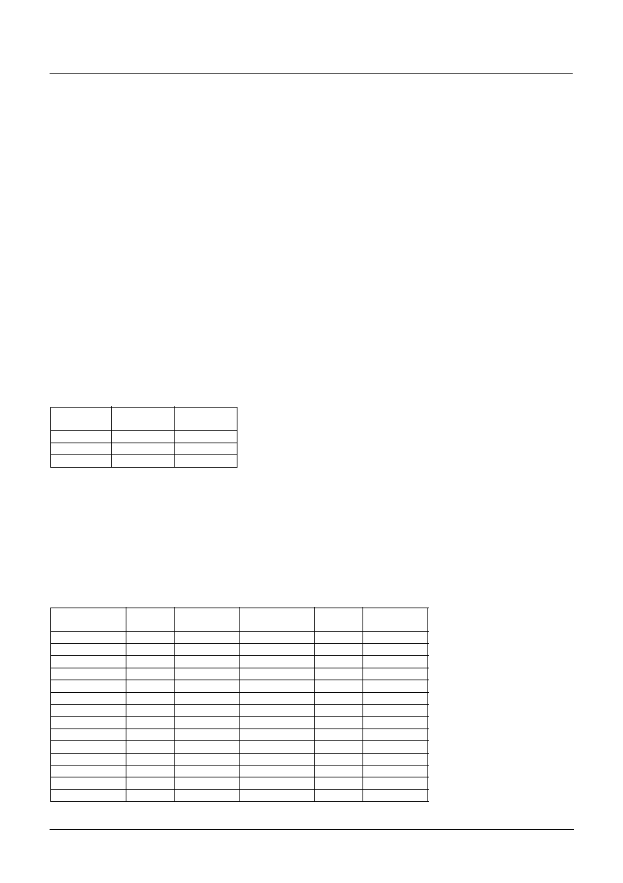
1.8.1 Internal Macrocells
Refer to STD90/MDL90.
1.8.2 Clock Drivers
STD90 max fanout for clock drivers
<condition>
∑
clock trunk width = 8 um
∑
clock trunk length = 5,000 um
∑
capacitance per fanout = 0.007838 pF
(= input capacitance for CK pin of fd1)
∑
standard load(SL) = 0.011 pF
(= input capacitance for iv)
∑
net length = 200 um per fanout
∑
max output transition time = 3.0 ns
∑
frequency
120 MHz
Table 1-1. Maximum Fanout of Clock Drivers
For a design with an operating frequency higher than 120 MHz, SEC strongly recommends using
clock tree synthesis.
1.8.3 I/O Cells
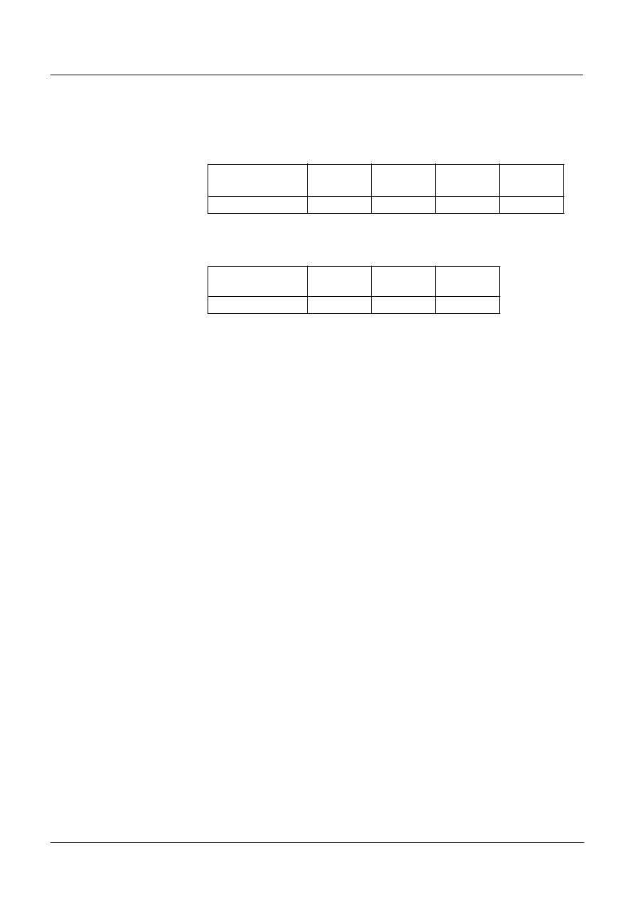
The maximum fanouts for I/O cells are as follows.
Table1-2. Maximum Fanouts of I/O cells(When input tr/tf = 1.6ns)
Cell Type
# of
Fanout
# of SL
CK2X
522
379
CK3X
703
511
CK4X
788
572
Cell Class
Output
Pin
Maximum
Fanouts
Cell Class
Output
Pin
Maximum
Fanouts
PHIC
Y
263
PHILI
Y
263
PHICD50
Y
264
PHILID50
Y
263
PHICU50
Y
264
PHILIU50
Y
263
PHIL
Y
262
PHISI
Y
263
PHILD50
Y
264
PHISID50
Y
263
PHILU50
Y
264
PHISIU50
Y
263
PHIS
Y
263
PHITATA
Y
264
PHISD50
Y
262
PHITU50ATA
Y
264
PHISU50
Y
263
PHITI
Y
263
PHIT
Y
264
PHITID50
Y
263
PHITD50
Y
264
PHITIU50
Y
264
PHITU50
Y
263
PHSOSCLF
Y
933
PHITU5
Y
263
PHSOSCMF
Y
1138
PHITU50C
Y
263
PHSOSCHF
Y
1860

INTRODUCTION
1.9 Product Line-Up
SEC ASIC
1-12
STDH90/MDL90
1.9 Product Line-Up
Refer to STD90/MDL90.

INTRODUCTION
1.10 Package Capability by Lead Count.
SEC ASIC
1-13
STDH90/MDL90
1.10 Package Capability by Lead Count.
Refer to STD90/MDL90.

INTRODUCTION
1.11 External Design Interface Considerations
SEC ASIC
1-14
STDH90/MDL90
1.11 External Design Interface Considerations
Refer to STD90/MDL90.

INTRODUCTION
1.12 Power Dissipation
SEC ASIC
1-15
STDH90/MDL90
1.12 Power Dissipation
Refer to STD90/MDL90.

Introduction
1.13 VDD/VSS Rules and Guidelines
SEC ASIC
1-16
STDH90/MDL90
1.13
VDD/VSS Rules
and Guidelines
There are three types of V
DD
and V
SS
in STDH90/MDL90, providing power with
internal and I/O pad area.
∑
Core logic
≠ VDD3I, VSSI
∑
Pre-drive (I/O area)
≠ VDD5P, VSSP
∑
Output-drive (I/O area)
≠ VDD5O, VSSO
The number of V
DD
and V
SS
pads required for a specific design depends on the
following factors:
∑
Number of input and output buffers
∑
Number of simultaneous switching outputs
∑
Number of used gates and simultaneous switching gates
∑
Operating frequency of the design.
1.13.1 Basic Placement Guidelines
The purpose of these guidelines is to minimize IR drop and noise for reliable
device operation.
∑
Core logic and pre-driver Vdd/Vss pads should be evenly distributed
on all sides of the chip.
∑
If you have core block demanding high power(compiled memory,analog)
, extra power pads should be placed on that side.
∑
Power pads for SSO group should be evenly distributed in the SSO group.
∑
Do not place the high drive output or bi-directional buffer next to a SSO
group.
∑
Opposite type power pads(Vdd/Vss) should be placed as close as possible.
Same type power pads(Vdd/Vdd,Vss/Vss) should be separated. These
two placement scheme will reduce the mutual inductance of lead of power
pads.
1.13.2 Core Logic V
DD
/V
SS
Bus and VDDI/VSSI Pad
Allocation Guidelines
The purpose of these guidelines is to ensure that minimum number of core logic
power pad pairs requirement based on electro-migration current limit. The
number of V
DD
/V
SS
pads required for a specific design is the function of the
operating frequency of a chip, i.e., designs operating at high frequency should
use more V
DD
/V
SS
pads.
∑
V
DD
bus width and pad requirements are equal to those of V
SS
.

1.13 VDD/VSS Rules and Guidelines
Introduction
STDH90/MDL90
1-17
SEC ASIC
∑
V
DD
/V
SS
buses and pads should be distributed evenly in the core and on
all sides of the chip.
∑
The total number of core logic V
DD
I pads required is equal to that of VSSI
pads
The number of VSSI/VDDI pad pairs required for a design can be calculated
from the following expression:
The number of VDDI/VSSI pad pairs =
|| (G x S x F x GC
eq_current
) + {
(P_i x F_i)} / I
em
|| round-up
In the above formula,
G = The core ( excluding hard macro blocks) size in gate counts
S = % of simultaneous switching gates (default = 0.2)
F = Switching frequency (MHz)
GC
eq_current
= Equivalent power(current) per gate(0.101uW/MHz/V)
P_i = Characterized power (current) for the i-th hard macro block(mA/MHz)
F_i = Switching frequency for the i-th hard macro block(MHz)
l
em
= Current limit per Vdd/Vss pad pairs based on electromigration rule.
(100mA)
For reliable device operation and minimum IR voltage drop, minimum number
of VSSI/VDDI pad pairs is 4.
Extra power may be needed for the demanding high power macro blocks
(SRAM,analog block,and so on)
1.13.3 Input Buffer V
DD
/V
SS
Pad VDDP/VSSP Allocation
Guidelines
These guidelines ensure that an adequate input threshold voltage margin is
maintained during a switching.
The number of VSSP/VDDP pad pairs required for a design can be
calculated from the following expression:
The number of VDDP/VSSP pad pairs =
|| Ieq_p / I
em
||round-up
in the above formula,
Ieq_p =
(Average current of input buffers and output pre-drivers
at maximum operating frequency)
l
em
= Current limit per Vdd/Vss pad pairs based on electro-migration rule.
(100 mA)
INTRODUCTION
1.13 VDD/VSS Rules and Guidelines
SEC ASIC
1-18
STDH90/MDL90
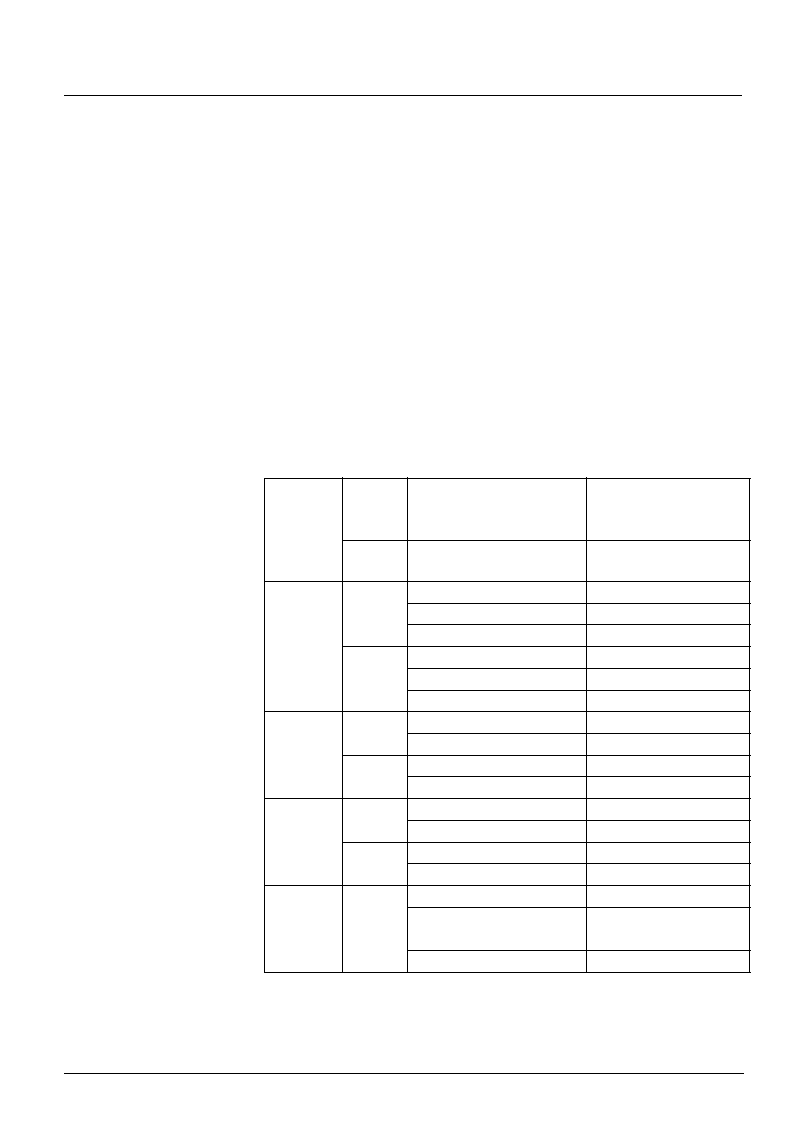
Table 1-3. leq_p(at F=100MHz) value of each input buffer and
output pre-driver.
Table 1-3(a). leq_p(at F=100MHz) value of each type of input buffer
Table 1-3(b). leq_p(at F=100MHz) value of each type of output
pre-driver
If buffer type is bi-directional, then you should combine the proper input buffer
and output pre-driver leq_p value.
For reliable device operation and minimum IR voltage drop, minimum number
of VSSP/VDDP pad pairs is 4.
In order to minimize number of power pads, you may use combined power pad.
You can get the combined power pad pairs VDDIP/VSSIP from the following
formula.
The number of VDDIP/VSSIP pad pairs =
|| (G x S x F x GC
eq_current
) + {
(P_i x F_i)} / I
em
+ Ieq_p / I
em
|| round-up
For reliable device operation and minimum IR voltage drop, minimum number
of VSSIP/VDDIP pad pairs is 4.
1.13.4 Output Buffer V
DD
/V
SS
Pad VDDO/VSSO Allocation
Guidelines
SSO(Simultaneous Switching Output) current induced in power and ground
inductance can cause system failure because of voltage fluctuations. In case of
output driver power pad calculation, we consider the SSO noise as well as
current limit based on electro-migration. We may define SSO as outputs are
considered to be simultaneous in 1ns window such as bus type buffers.
The number of VDDO/VSSO pads required for a device can be calculated
from the following expressions.
∑
The number of power pads for each SSO group from the following formula.
NVDDO
each_sso
= (number_of_SSO x L
lead
) / (D
sso_mode
x NB
vdd
)
NVSSO
each_sso
= (number_of_SSO x L
lead
) / (D
sso_mode
x NB
vss
)
in the above formula,
Input Buffer Type
CMOS
CMOS
Schmitt
TTL
TTL
Schmitt
Ieq_p(mA)
0.37
0.45
0.30
0.53
Output
Slew-Rate Type
Normal
Medium
High
Ieq_p(mA)
1.0
1.2
1.8
INTRODUCTION
1.13 VDD/VSS Rules and Guidelines
SEC ASIC
1-19
STDH90/MDL90
NVDDO
each_sso
= the number of VDDO pads required for each SSO group
NVSSO
each_sso
= the number of VSSO pads required for each SSO group
NB
vdd
= the number of buffers per VDD power pad with 1nH lead
inductance
NB
vss
= the number of buffers per VSS ground pad with 1nH lead
inductance
L
lead
= lead frame inductance of package
(Refer to 1.10 Package Capability by Lead Count)
D
sso_mode
= D
L_mode
x D
P_mode
x D
V_mode
x D
T_mode
x D
C_mode
D
L_mode
: Lead inductance derating factor
D
P_mode
: Process derating factor
D
V_mode
: Voltage derating factor
D
T_mode
: Temperature derating factor
D
C_mode
: C
load
derating factor
(mode is either vdd or vss. Refer to Table 1.4)
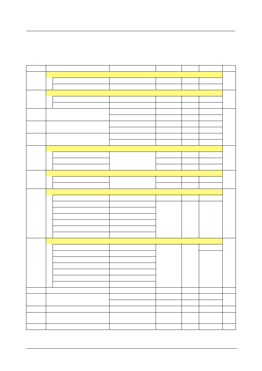
Table 1-4. Derating Equation
Item
Mode
Equation
Range
Package
Lead
D
L_vdd
0.0052 * Lpg + 0.9794
-0.0052 * Lpg + 1.0825
3nH
Lpg
10nH
10nH
<
Lpg
15nH
D
L_vss
-0.0094 * Lpg + 1.0377
0.0377 * Lpg + 0.5660
3nH
Lpg
10nH
10nH
<
Lpg
15nH
Process
D
P_vdd
1
best
1.1134
typical
1.2887
worst
D
P_vss
1
best
1.3208
typical
1.5094
worst
Voltage
D
V_vdd
-0.2222 * voltage + 2.1556
4.5
voltage
5.0
-0.1778 * voltage + 2.9333
5.0
<
voltage
5.5
D
V_vdd
-0.2500 * voltage + 2.2812
4.5
voltage
5.0
-0.1250 * voltage + 1.6562
5.0
<
voltage
5.5
Temp.
D
T_vdd
0.0008 * temp + 1.0000
-40
temp
25
0.0006 * temp + 1.0066
25
<
temp
125
D
T_vdd
0.0045 * temp + 1.0000
-40
temp
25
0.0034 * temp + 1.0274
25
<
temp
125
Cload
D
C_vdd
0.0155 * Cload + 0.5361
10pF
Cload
30pF
0.0180 * Cload + 0.4588
30pF
<
Cload
100pF
D
C_vdd
0.0255 * Cload + 0.2358
10pF
Cload
30pF
0.0142 * Cload + 0.5755
30pF
<
Cload
100pF

INTRODUCTION
1.13 VDD/VSS Rules and Guidelines
SEC ASIC
1-20
STDH90/MDL90
∑
The number of power pads for total SSO groups from the following
formula.
NVDDO
sso
=
NVDDO
each_sso
NVSSO
sso
=
NVSSO
each_sso
in the above formula,
NVDDO
sso
= the number of VDDO pads required for total SSO groups
NVSSO
sso
= the number of VSSO pads required for total SSO groups
∑
The number of power pads for non-SSO group from the following formula.
N
NSvddo
= I
eq_o
/ I
em
N
NSvsso
= I
eq_o
/ I
em
in the above formula,
I
eq_o
=
(C
load
x V x F x P)
non-SSO
C
load
: output load capacitance
V : operating voltage
F : operating frequency
P : I/O switching percent(marginal=0.5)
I
em
: Current density based on electro-migration rule(100mA)
∑
The total number of power pads for VDDO from the following formula.
||
(number_of_SSO x L
lead
) / (D
sso_mode
x NB
vdd
) + I
eq_o
/ I
em
|| round-up
∑
The total number of power pads for VSSO from the following formula.
||
(number_of_SSO x L
lead
) / (D
sso_mode
x NB
vss
)+ I
eq_o
/ I
em
) || round-up
If you use open-drain type buffers, you can consider only VSSO power pads
because they have only current sink.
Table 1-5. NBvdd/NBvss Parameter
(Condition : Process=best , Voltage=5.25V , Temp=0
∞
C , Cload=30pF)
Buffer
Type
Normal
Medium
High
NBvdd
NBvss
NBvdd
NBvss
NBvdd
NBvss
B2
170
116
B4
84
55
89
58
B8
39
28
40
29
B12
28
20
30
21
31
22
B16
23
16
24
17
26
18
B24
19
13
20
14
22
15

1.14 Crystal Oscillator Consideration
Introduction
STDH90/MDL90
1-21
SEC ASIC
1.14 Crystal Oscillator Consideration
Refer to STD90/MDL90.

2
Electrical Characteristics

Contents
DC Electrical Characteristics ......................................................................................... 2-1
Input Buffer DC Curves.................................................................................................. 2-3
Output Drive Capabilities ............................................................................................... 2-5
ELECTRICAL CHARACTERISTICS
DC ELECTRICAL CHARACTERISTICS
SEC ASIC
2-1
STDH90/MDL90
DC ELECTRICAL CHARACTERISTICS
V
DD
= 5.0
±
0.5V, T
A
= 0 to 70
∞
C (In case of 5V Interface IO)
Symbol
Parameter
Condition
Min
Typ
Max
Unit
V
IH
High level input voltage
V
CMOS interface
3.5
TTL interface
2.0
V
IL
Low level input voltage
V
CMOS interface
1.5
TTL interface
0.8
VT
Switching threshold
CMOS
2.45
V
TTL
1.45
VT+
Schmitt trigger, positive-going
threshold
CMOS
3.0
3.5
TTL
1.8
2.0
VT-
Schmitt trigger, negative-going
threshold
CMOS
1.5
2.0
TTL
0.8
1.1
I
IL
Low level input current
µ
A
Input buffer
V
IN
= VSS
≠10
10
Input buffer with 50K pull-up
-200
-100
-10
Input buffer with 5K pull-up
-2000
-1000
-10
I
IH
High level input current
µ
A
Input buffer
V
IN
= VDD
≠10
10
Input buffer with pull-down
10
100
200
V
OH
High level output voltage
V
Type B2 to B24Note1
I
OH
= ≠1
µ
A
VDD ≠ 0.05
Type B2
I
OH
= ≠2mA
2.4
Type B4
I
OH
= ≠4mA
Type B8
I
OH
= ≠8mA
Type B12
I
OH
= ≠12mA
Type B16
I
OH
= ≠16mA
Type B24
I
OH
= ≠24mA
V
OL
Low level output voltage
V
Type B2 to B24 Note1
I
OL
= 1
µ
A
0.05
Type B2
I
OL
= 2mA
0.4
Type B4
I
OL
= 4mA
Type B8
I
OL
= 8mA
Type B12
I
OL
= 12mA
Type B16
I
OL
= 16mA
Type B24
I
OL
= 24mA
I
OZ
Tri-state output leakage current
V
OUT
=VSS or VDD
≠10
10
µ
A
I
OS
Output short circuit current
V
DD
= 5.5V, VO = VDD
233
mA
V
DD
= 5.5V, VO = VSS
≠233
I
DD
Quiescent supply current
V
IN
= VSS or VDD
100 Note2
µ
A
C
IN
Input capacitance Note3
Any Input and
Bidirectional Buffers
4
pF
C
OUT
Output capacitance Note3
Any Output Buffer
4
pF
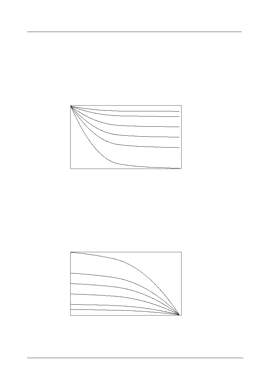
INPUT BUFFER DC CURVES
ELECTRICAL CHARACTERISTICS
STDH90/MDL90
2-2
SEC ASIC
NOTES:
1.
Type B2 means 2mA output driver cells, and Type B8/B24 means 8mA/24mA output driver cells.
2.
This value depends on the customer design.
3.
This value exclude package parasitics.
Absolute Maximum Ratings
Recommended Operating Conditions
INPUT BUFFER DC CURVES
Input Buffer Transfer Curves(CMOS)
V
DD
= 5.0V, T
A
= 25
∞
C, Typical Process
Symbol
Parameter
Rating
Unit
V
DD
DC supply voltage
≠ 0.3 to 7
V
V
IN
DC input voltage
3.3V I/O
-0.3 to 3.6
V
5.0V I/O
-0.3 to 5.5
I
IN
DC input current
±
10
mA
T
STG
Storage temperature
≠ 40 to 125
∞
C
Symbol
Parameter
Rating
Unit
V
DD
DC supply voltage
5V
4.5 to 5.5
V
3.3V
3.0 to 3.6
V
T
A
Commercial temperature range
0 to 70
∞
C
Industrial temperature range
≠ 40 to 85
V(PAD) [V]
1.0
2.0
3.0
4.0
5.0
V(Y) [V]
1.0
2.0
3.0
3.3
ELECTRICAL CHARACTERISTICS
INPUT BUFFER DC CURVES
SEC ASIC
2-3
STDH90/MDL90
Input Buffer Transfer Curves(TTL)
V
DD
= 5.0V, T
A
= 25
∞
C, Typical Process
Input Buffer Transfer Curves(CMOS SCHMITT TRIGGER)
V
DD
= 5.0V, T
A
= 25
∞
C, Typical Process
V(PAD) [V]
1.0
2.0
3.0
4.0
5.0
V(Y) [V]
1.0
2.0
3.0
3.3
V(PAD) [V]
1.0
2.0
3.0
4.0
5.0
V(Y) [V]
1.0
2.0
3.0
3.3
INPUT BUFFER DC CURVES
ELECTRICAL CHARACTERISTICS
STDH90/MDL90
2-4
SEC ASIC
Input Buffer Transfer Curves(TTL SCHMITT TRIGGER)
V
DD
= 5.0V, T
A
= 25
∞
C, Typical Process
V(PAD) [V]
1.0
2.0
3.0
4.0
5.0
V(Y) [V]
1.0
2.0
3.0
3.3
ELECTRICAL CHARACTERISTICS
OUTPUT DRIVE CAPABILITIES
SEC ASIC
2-5
STDH90/MDL90
OUTPUT DRIVE CAPABILITIES
Output Buffer Transfer Curves(Pull Down)
IV Characteristics [V
DD
= 5.0V, T
A
= 25
∞
C, Typical Process]
Output Buffer Transfer Curves(Pull Up)
IV Characteristics [V
DD
= 5.0V, T
A
= 25
∞
C, Typical Process]
V(PAD) [V]
1.0
2.0
3.0
4.0
5.0
I(PAD) [mA]
-165
-150
-125
-100
-75
-50
-25
PHOB2
PHOB4
PHOB8
PHOB12
PHOB16
PHOB24
V(PAD) [V]
1.0
2.0
3.0
4.0
5.0
I(PAD) [mA]
25
50
75
100
125
150
180
PHOB2
PHOB4
PHOB8
PHOB12
PHOB16
PHOB24

3
Internal Macrocells
(Refer to STD90/MDL90)

4
Input/Output Cells

Contents
Overview...............................................................................................................................4-1
Summary Tables ................................................................................................................... 4-2
Input Buffers .........................................................................................................................4-6
Output Buffers ...................................................................................................................... 4-21
Bi-Directional Buffers ............................................................................................................ 4-41
Clock Drivers ........................................................................................................................ 4-43
Oscillators.............................................................................................................................4-46
ATA2 Interface ...................................................................................................................... 4-53
ATA3 Interface ...................................................................................................................... 4-62
I/O with unbalanced output impedance ................................................................................ 4-69
I/O with controlled pull-up ..................................................................................................... 4-73
Power Pads ..........................................................................................................................4-77
Analog Interface ................................................................................................................... 4-78
DRAM Interface .................................................................................................................... 4-79
Customized I/O..................................................................................................................... 4-80

INPUT/OUTPUT CELLS
OVERVIEW
SEC ASIC
4-1
STDH90/MDL90
OVERVIEW
This chapter describes various kinds of 5V-interface I/O cells in STDH90/MDLH90 library.
The switching characteristics of each cell are attached to its basic cell information. The AC characteristics of
bi-directional buffers are not included in this data sheet. However, they can be derived from different
combinations of input and output cells.
There are so many possible combinations of input/output cells, therefore, the naming conventions are
adopted to help you memorize and use this cell library efficiently. You can refer to the naming conventions
contained in "Summary Tables" section.
The "Summary Tables" section shows the list of 5V-interface I/O cells separated by the category (input,
output, bi-directional, etc.), and the more detailed description tables can be found on the leading part of
each category.
All 5V-interface I/O cells use 1 I/O slot except for oscillators with 2 I/O slots.
SUMMARY TABLES
INPUT/OUTPUT CELLS
STDH90/MDL90
4-2
SEC ASIC
SUMMARY TABLES
Input Cells
<Naming Convention of Input Buffers>
Output Buffers
Cell Type
Cell Name
Page
CMOS Level
PHIC/PHICD50/PHICU50
4-7
TTL Level
PHIT/PHITD50/PHITU50/PHITU5
PHITI/PHITID50/PHITIU50
4-9
4-11
CMOS Schmitt Trigger Level
PHIS/PHISD50/PHISU50
PHISI/PHISID50/PHISIU50
4-13
4-15
TTL Schmitt Trigger Level
PHIL/PHILD50/PHILU50
PHILI/PHILID50/PHILIU50
4-17
4-19
PHvlab
v
a
b
C
CMOS level
None
Non-inverting
None
No resistor
T
TTL level
I
Inverting
D50
Pull-down resistor(50K)
S
CMOS Schmitt Trigger level
U5
Pull-up resistor(5K)
L
TTL Schmitt Trigger level
U50
Pull-up resistor(50K)
Cell Type
Cell Name
Current Drive (mA)
Page
Normal
PHOBy
2/4/8/12/16/24
4-22
PHOBySM
4/8/12/16/24
PHOBySH
12/16/24
Open Drain
PHODy
2/4/8/12/16/24
4-27
PHODySM
4/8/12/16/24
PHODySH
12/16/24
Tri-State
PHOTy
2/4/8/12/16/24
4-33
PHOTySM
4/8/12/16/24
PHOTySH
12/16/24
INPUT/OUTPUT CELLS
SUMMARY TABLES
SEC ASIC
4-3
STDH90/MDL90
<Naming Convention of Output Cells>
Bi-Directional Buffers
<Naming Convention of Bi-Directional Buffers>
Clock Drivers
<Naming Convention of Clock Drivers>
PH O x y z
x
y
B
Normal buffer
2
2mA drive
D
Open drain buffer
4
4mA drive
T
Tri-state buffer
8
8mA drive
z
12
12mA drive
None
No slew-rate control
16
16mA drive
SM
Medium slew-rate control
24
24mA drive
SH
High slew-rate control
Cell Type
Cell Name
Page
Open Drain
PHBaDyz/PHBaU50Dyz
4-42
Tri-State
PHBaTyz/PHBaD50Tyz/PHBaU50Tyz
P HB a b x y z
a
y
C
CMOS level
2
2mA drive
T
TTL level
4
4mA drive
S
CMOS Schmitt Trigger level
8
8mA drive
L
TTL Schmitt Trigger level
12
12mA drive
z
16
16mA drive
None
No slew-rate control
24
24mA drive
SM
Medium slew -rate control
SH
High slew-rate control
Cell Type
Cell Name
Current Drive (mA)
Page
CMOS Level
CKyX
2/3/4
4-44
CKyX
y
# of SL
2
379
3
511
4
572
SUMMARY TABLES
INPUT/OUTPUT CELLS
STDH90/MDL90
4-4
SEC ASIC
Oscillators
ATA2 Interface with no fail-safe
ATA3 Interface with fail-safe
I/O with unbalanced output impedance
I/O with controlled pull-up
Cell Type
Cell Name
Page
Oscillators
PHSOSCLF(1KHz ~ 10MHz)
4-47
PHSOSCMF(10MHz ~ 25MHz)
4-49
PHSOSCHF(50MHz and 60MHz)
4-51
Cell Type
Cell Name
Page
ATA2 Output
PHOD24ATA2
PHOT24ATA2
4-54
4-55
Controlled ATA2 Output
PHOT24CATA2/PHOTC24ATA2
PHOTC8ATA2/PHOT8CATA2
4-56
ATA2 Bi-Directional
PHBLU50D24ATA2
PHBTU50T24ATA2
4-59
4-60
Controlled ATA2 Bi-Directional
PHBLU50TC8ATA2
PHBLU50T8CATA2
4-61
Cell Type
Cell Name
Page
ATA3 Input
PHITATA
PHITU50ATA
4-63
ATA3 Output
PHSOT12S1FATA
PHSOT4S1FATA
4-65
ATA3 Bi-Directional
PHSBTT4S1FATA
PHSBTT12S1FATA
PHSBTU50T4S1FATA
PHSBTU50T12S1FATA
4-67
4-68
Cell Type
Cell Name
Page
Unbalanced Output
PHOT24S4F
4-70
Unbalanced Bi-Directional
PHBTT24S4F
4-71
Unbalanced Bi-Directional with Controlled Pull-Up
PHBTU50CT24S4F
4-72
Cell Type
Cell Name
Page
Controlled Input
PHITU50C
4-74
Controlled Bi-Directional
PHBTU50CD2/PHBTU50CD4
PHBTU50CT2/PHBTU50CT4
4-75
4-76
INPUT/OUTPUT CELLS
SUMMARY TABLES
SEC ASIC
4-5
STDH90/MDL90
Power Pads
Analog Interface
DRAM Interface
Customized I/O
Cell Type
Cell Name
Page
I/O VDD
VDD5(P/O/OP)
4-77
CORE VDD
VDD3I
I/O VSS
VSS(P/O/OP)
CORE VSS
VSSI
VBB
VBB
Cell Type
Cell Name
Page
VDD Power Pad
VCCA
4-78
VSS Power Pads
VSSA
Analog Input with Seperated Bluk-Bias
PICA
PICA_10
PICA_25
PICA_500
Analog Output with Seperated Bluk-Bias
POBA
Cell Type
Cell Name
Page
VDD Power Pad
VCCD
4-79
VSS Power Pad
VSSD
DRAM DCPAD with 50K Pull-Up
DCPAD_PD50K
DRAM DCPAD
DCPAD
Cell Type
Cell Name
Page
Inverting Output
PHOTI4
4-81
Bi-Directional with Inverting Output
PHBTTI4
4-82
SEC ASIC
4-6
STDH90/MDL90
INPUT CELLS
Cell List
Cell Name
Function Description
PHIC/PHICD50/PHICU50
5V CMOS Level Input Buffers
PHIT/PHITD50/PHITU50
5V TTL Level Input Buffers
PHITI/PHITID50/PHITIU50/PHITU5
5V TTL Level Input Inverters
PHIS/PHISD50/PHISU50
5V CMOS Schmitt Trigger Level Input Buffers
PHISI/PHISID50/PHISIU50
5V CMOS Schmitt Trigger Level Input Inverters
PHIL/PHILD50/PHILU50
5V TTL Schmitt Trigger Level Input Buffers
PHILI/PHILID50/PHILIU50
5V TTL Schmitt Trigger Level Input Inverters
STDH90/MDL90
4-7
SEC ASIC
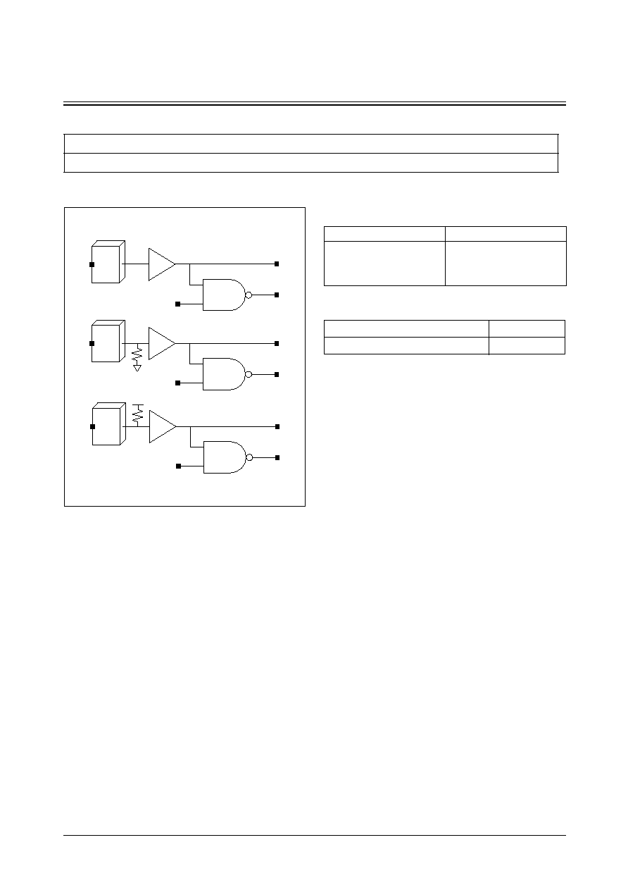
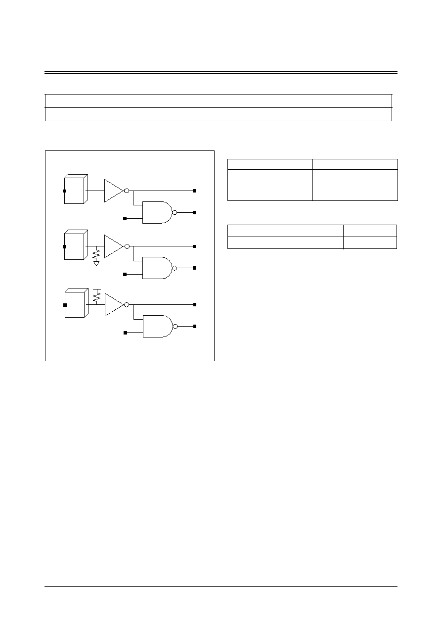
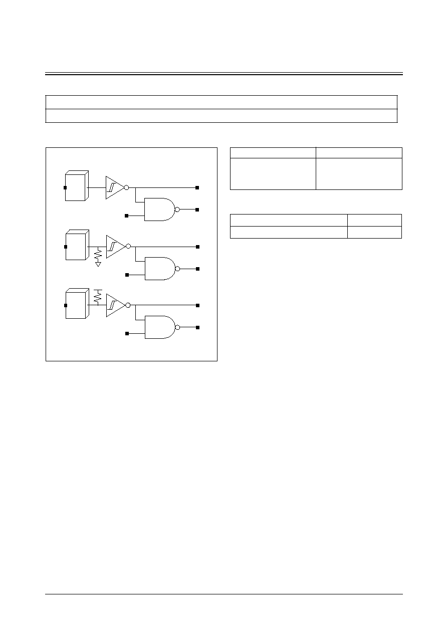
PHIC/PHICD50/PHICU50
CMOS Level Input Buffers
Cell Availability
Logic Symbol
5V Interface
PHIC/PHICD50/PHICU50
Y
PO
PI
PAD
Y
PO
PI
PAD
Y
PO
PI
PAD
PHIC
PHICD50
PHICU50
Truth Table
Standard Load (SL)
PAD
PI
Y
PO
1
1
1
0
0
x
0
1
1
0
1
1
Cell Name
PI
PHIC/PHICD50/PHICU50
2.3
SEC ASIC
4-8
STDH90/MDL90
PHIC/PHICD50/PHICU50
CMOS Level Input Buffers
PHIC Switching Characteristics
[Delays for typical process, 25 C, 5.0V, when t , t = 0.80ns]
o
R F
(SL : Standard Load)
Path
Parameter
Delay [ns]
SL = 2
Delay Equations [ns]
Group1*
Group2*
Group3*
PAD to Y
tR
0.135
0.114 + 0.011*SL
0.113 + 0.011*SL
0.101 + 0.011*SL
tF
0.192
0.185 + 0.004*SL
0.159 + 0.009*SL
0.161 + 0.009*SL
tPLH
0.415
0.403 + 0.006*SL
0.405 + 0.005*SL
0.414 + 0.005*SL
tPHL
0.884
0.865 + 0.010*SL
0.881 + 0.006*SL
0.920 + 0.005*SL
*Group1 : SL < 4, *Group2 : 4 SL 46, *Group3 : 46 < SL
< <
= =
PHICD50 Switching Characteristics
[Delays for typical process, 25 C, 5.0V, when t , t = 0.80ns]
o
R F
(SL : Standard Load)
Path
Parameter
Delay [ns]
SL = 2
Delay Equations [ns]
Group1*
Group2*
Group3*
PAD to Y
tR
0.138
0.112 + 0.013*SL
0.122 + 0.011*SL
0.106 + 0.011*SL
tF
0.189
0.167 + 0.011*SL
0.178 + 0.009*SL
0.160 + 0.009*SL
tPLH
0.458
0.446 + 0.006*SL
0.449 + 0.005*SL
0.459 + 0.005*SL
tPHL
0.889
0.871 + 0.009*SL
0.884 + 0.006*SL
0.921 + 0.005*SL
*Group1 : SL < 4, *Group2 : 4 SL 46, *Group3 : 46 < SL
< <
= =
PHICU50 Switching Characteristics
[Delays for typical process, 25 C, 5.0V, when t , t = 0.80ns]
o
R F
(SL : Standard Load)
Path
Parameter
Delay [ns]
SL = 2
Delay Equations [ns]
Group1*
Group2*
Group3*
PAD to Y
tR
0.133
0.114 + 0.010*SL
0.108 + 0.011*SL
0.098 + 0.011*SL
tF
0.186
0.172 + 0.007*SL
0.161 + 0.009*SL
0.163 + 0.009*SL
tPLH
0.399
0.387 + 0.006*SL
0.391 + 0.005*SL
0.411 + 0.005*SL
tPHL
0.912
0.893 + 0.010*SL
0.910 + 0.006*SL
0.951 + 0.005*SL
*Group1 : SL < 4, *Group2 : 4 SL 46, *Group3 : 46 < SL
< <
= =
STDH90/MDL90
4-9
SEC ASIC
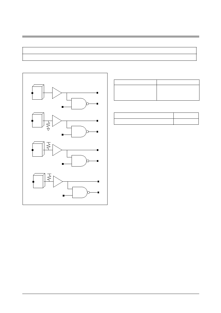
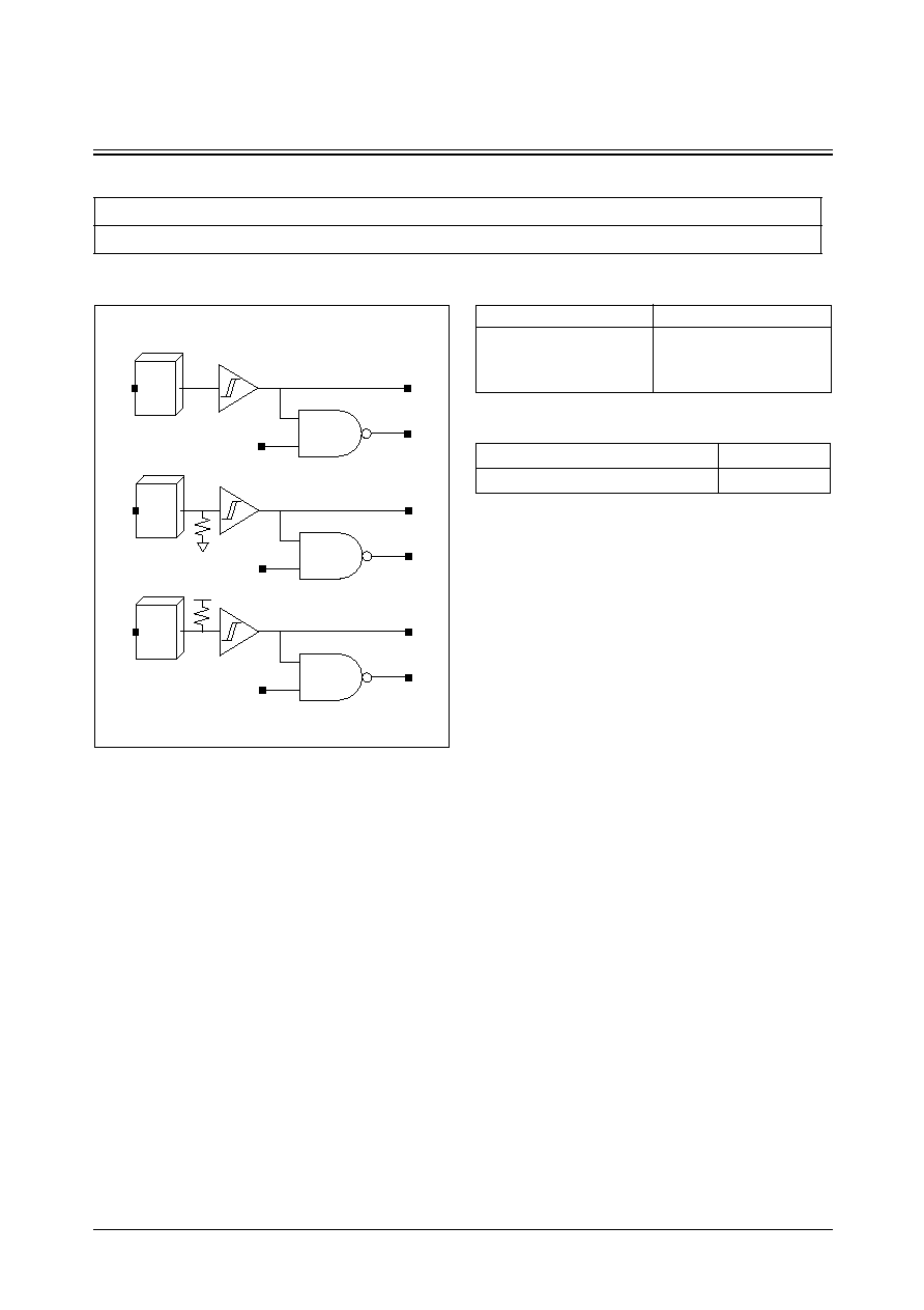
PHIT/PHITD50/PHITU50/PHITU5
TTL Level Input Buffers
Cell Availability
Logic Symbol
5V Interface
PHIT/PHITD50/PHITU50
Y
PO
PI
PAD
Y
PO
PI
PAD
Y
PO
PI
PAD
PHIT
PHITD50
PHITU50
Y
PO
PI
PAD
PHITU5
Truth Table
Standard Load (SL)
PAD
PI
Y
PO
1
1
1
0
0
x
0
1
1
0
1
1
Cell Name
PI
PHIT/PHITD50/PHITU50/PHITU5
2.3

SEC ASIC
4-10
STDH90/MDL90
PHIT/PHITD50/PHITU50/PHITU5
TTL Level Input Buffers
PHIT Switching Characteristics
[Delays for typical process, 25 C, 5.0V, when t , t = 0.80ns]
o
R F
(SL : Standard Load)
Path
Parameter
Delay [ns]
SL = 2
Delay Equations [ns]
Group1*
Group2*
Group3*
PAD to Y
tR
0.136
0.116 + 0.010*SL
0.113 + 0.011*SL
0.099 + 0.011*SL
tF
0.198
0.181 + 0.009*SL
0.180 + 0.009*SL
0.165 + 0.009*SL
tPLH
0.575
0.563 + 0.006*SL
0.566 + 0.005*SL
0.576 + 0.005*SL
tPHL
0.913
0.893 + 0.010*SL
0.912 + 0.006*SL
0.955 + 0.005*SL
*Group1 : SL < 4, *Group2 : 4 SL 46, *Group3 : 46 < SL
< <
= =
PHITD50 Switching Characteristics
[Delays for typical process, 25 C, 5.0V, when t , t = 0.80ns]
o
R F
(SL : Standard Load)
Path
Parameter
Delay [ns]
SL = 2
Delay Equations [ns]
Group1*
Group2*
Group3*
PAD to Y
tR
0.142
0.123 + 0.009*SL
0.116 + 0.011*SL
0.098 + 0.011*SL
tF
0.210
0.203 + 0.003*SL
0.178 + 0.009*SL
0.163 + 0.009*SL
tPLH
0.624
0.612 + 0.006*SL
0.616 + 0.005*SL
0.626 + 0.005*SL
tPHL
0.939
0.922 + 0.008*SL
0.933 + 0.006*SL
0.980 + 0.005*SL
*Group1 : SL < 4, *Group2 : 4 SL 46, *Group3 : 46 < SL
< <
= =
PHITU50 Switching Characteristics
[Delays for typical process, 25 C, 5.0V, when t , t = 0.80ns]
o
R F
(SL : Standard Load)
Path
Parameter
Delay [ns]
SL = 2
Delay Equations [ns]
Group1*
Group2*
Group3*
PAD to Y
tR
0.139
0.115 + 0.012*SL
0.121 + 0.011*SL
0.106 + 0.011*SL
tF
0.210
0.203 + 0.003*SL
0.178 + 0.009*SL
0.163 + 0.009*SL
tPLH
0.558
0.546 + 0.006*SL
0.549 + 0.005*SL
0.560 + 0.005*SL
tPHL
0.939
0.922 + 0.008*SL
0.933 + 0.006*SL
0.978 + 0.005*SL
*Group1 : SL < 4, *Group2 : 4 SL 46, *Group3 : 46 < SL
< <
= =
PHITU5 Switching Characteristics
[Delays for typical process, 25 C, 5.0V, when t , t = 0.80ns]
o
R F
(SL : Standard Load)
Path
Parameter
Delay [ns]
SL = 2
Delay Equations [ns]
Group1*
Group2*
Group3*
PAD to Y
tR
0.139
0.116 + 0.012*SL
0.120 + 0.011*SL
0.101 + 0.011*SL
tF
0.183
0.152 + 0.016*SL
0.184 + 0.009*SL
0.162 + 0.009*SL
tPLH
0.427
0.413 + 0.007*SL
0.419 + 0.005*SL
0.427 + 0.005*SL
tPHL
1.073
1.053 + 0.010*SL
1.072 + 0.006*SL
1.112 + 0.005*SL
*Group1 : SL < 4, *Group2 : 4 SL 46, *Group3 : 46 < SL
< <
= =
STDH90/MDL90
4-11
SEC ASIC
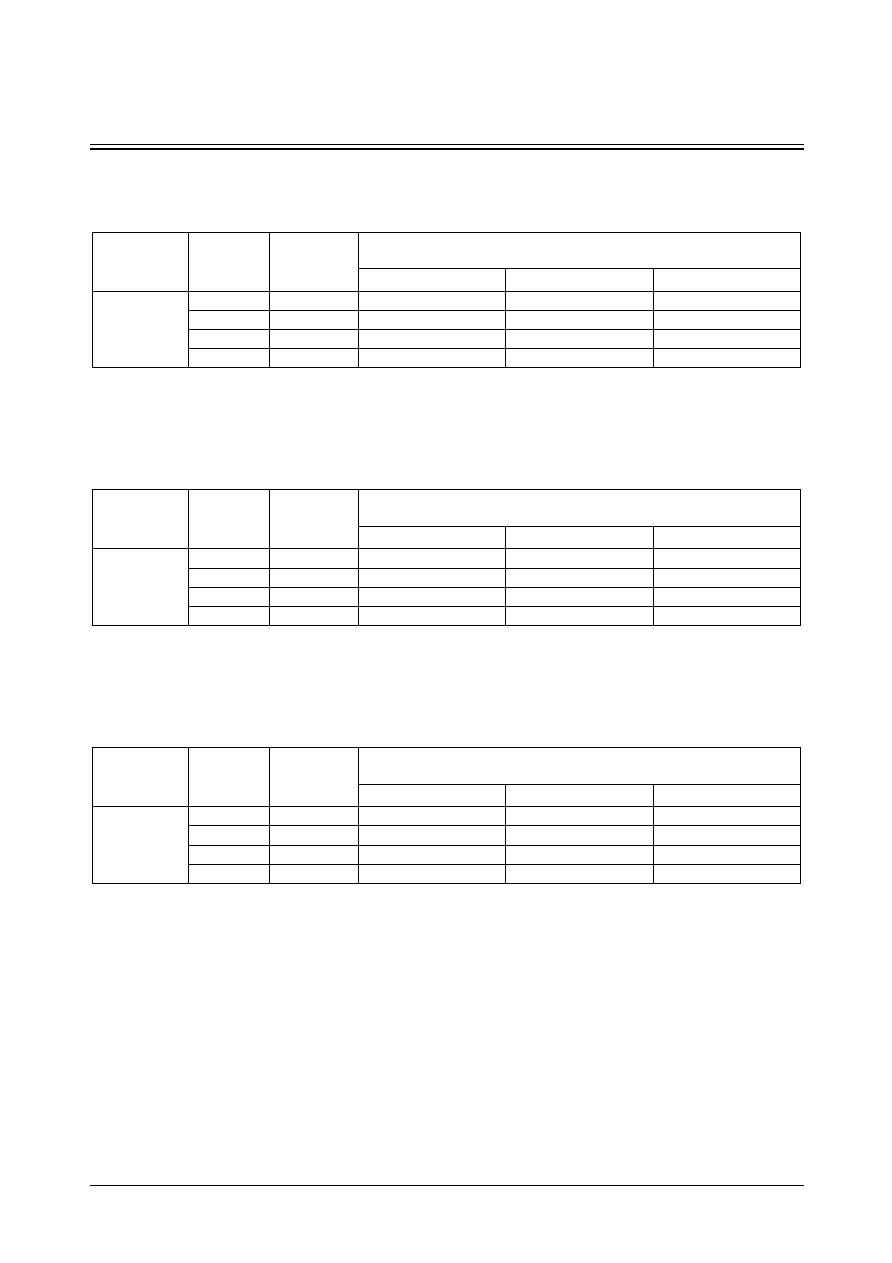
PHITI/PHITID50/PHITIU50
TTL Level Input Inverters
Cell Availability
Logic Symbol
5V Interface
PHITI/PHITID50/PHITIU50
Y
PO
PI
PAD
Y
PO
PI
PAD
Y
PO
PI
PAD
PHITI
PHITID50
PHITIU50
Truth Table
Standard Load (SL)
PAD
PI
Y
PO
0
1
1
0
1
x
0
1
0
0
1
1
Cell Name
PI
PHITI/PHITID50/PHITIU50
2.3
SEC ASIC
4-12
STDH90/MDL90
PHITI/PHITID50/PHITIU50
TTL Level Input Inverters
PHITI Switching Characteristics
[Delays for typical process, 25 C, 5.0V, when t , t = 0.80ns]
o
R F
(SL : Standard Load)
Path
Parameter
Delay [ns]
SL = 2
Delay Equations [ns]
Group1*
Group2*
Group3*
PAD to Y
tR
0.134
0.114 + 0.010*SL
0.111 + 0.011*SL
0.099 + 0.011*SL
tF
0.188
0.171 + 0.009*SL
0.170 + 0.009*SL
0.151 + 0.009*SL
tPLH
0.659
0.647 + 0.006*SL
0.651 + 0.005*SL
0.659 + 0.005*SL
tPHL
0.989
0.970 + 0.009*SL
0.986 + 0.006*SL
1.011 + 0.005*SL
*Group1 : SL < 4, *Group2 : 4 SL 46, *Group3 : 46 < SL
< <
= =
PHITID50 Switching Characteristics
[Delays for typical process, 25 C, 5.0V, when t , t = 0.80ns]
o
R F
(SL : Standard Load)
Path
Parameter
Delay [ns]
SL = 2
Delay Equations [ns]
Group1*
Group2*
Group3*
PAD to Y
tR
0.139
0.115 + 0.012*SL
0.121 + 0.011*SL
0.102 + 0.011*SL
tF
0.188
0.171 + 0.009*SL
0.169 + 0.009*SL
0.160 + 0.009*SL
tPLH
0.685
0.673 + 0.006*SL
0.676 + 0.005*SL
0.690 + 0.005*SL
tPHL
1.039
1.020 + 0.009*SL
1.036 + 0.006*SL
1.062 + 0.005*SL
*Group1 : SL < 4, *Group2 : 4 SL 46, *Group3 : 46 < SL
< <
= =
PHITIU50 Switching Characteristics
[Delays for typical process, 25 C, 5.0V, when t , t = 0.80ns]
o
R F
(SL : Standard Load)
Path
Parameter
Delay [ns]
SL = 2
Delay Equations [ns]
Group1*
Group2*
Group3*
PAD to Y
tR
0.139
0.116 + 0.012*SL
0.120 + 0.011*SL
0.102 + 0.011*SL
tF
0.180
0.147 + 0.017*SL
0.184 + 0.009*SL
0.156 + 0.009*SL
tPLH
0.685
0.673 + 0.006*SL
0.676 + 0.005*SL
0.690 + 0.005*SL
tPHL
0.973
0.953 + 0.010*SL
0.972 + 0.006*SL
1.016 + 0.005*SL
*Group1 : SL < 4, *Group2 : 4 SL 46, *Group3 : 46 < SL
< <
= =
STDH90/MDL90
4-13
SEC ASIC
PHIS/PHISD50/PHISU50
CMOS Schmitt Trigger Level Input Buffers
Cell Availability
Logic Symbol
5V Interface
PHIS/PHISD50/PHISU50
Y
PO
PI
PAD
Y
PO
PI
PAD
Y
PO
PI
PAD
Truth Table
Standard Load (SL)
PAD
PI
Y
PO
1
1
1
0
0
x
0
1
1
0
1
1
Cell Name
PI
PHIS/PHISD50/PHISU50
2.3
PHIS
PHISD50
PHISU50
SEC ASIC
4-14
STDH90/MDL90
PHIS/PHISD50/PHISU50
CMOS Schmitt Trigger Level Input Buffers
PHIS Switching Characteristics
[Delays for typical process, 25 C, 5.0V, when t , t = 0.80ns]
o
R F
(SL : Standard Load)
Path
Parameter
Delay [ns]
SL = 2
Delay Equations [ns]
Group1*
Group2*
Group3*
PAD to Y
tR
0.138
0.121 + 0.009*SL
0.111 + 0.011*SL
0.105 + 0.011*SL
tF
0.197
0.180 + 0.008*SL
0.178 + 0.009*SL
0.165 + 0.009*SL
tPLH
0.494
0.482 + 0.006*SL
0.485 + 0.005*SL
0.494 + 0.005*SL
tPHL
1.022
1.002 + 0.010*SL
1.021 + 0.006*SL
1.064 + 0.005*SL
*Group1 : SL < 4, *Group2 : 4 SL 46, *Group3 : 46 < SL
< <
= =
PHISD50 Switching Characteristics
[Delays for typical process, 25 C, 5.0V, when t , t = 0.80ns]
o
R F
(SL : Standard Load)
Path
Parameter
Delay [ns]
SL = 2
Delay Equations [ns]
Group1*
Group2*
Group3*
PAD to Y
tR
0.132
0.108 + 0.012*SL
0.115 + 0.011*SL
0.104 + 0.011*SL
tF
0.194
0.178 + 0.008*SL
0.172 + 0.009*SL
0.165 + 0.009*SL
tPLH
0.523
0.509 + 0.007*SL
0.516 + 0.005*SL
0.528 + 0.005*SL
tPHL
1.040
1.019 + 0.011*SL
1.040 + 0.006*SL
1.083 + 0.005*SL
*Group1 : SL < 4, *Group2 : 4 SL 46, *Group3 : 46 < SL
< <
= =
PHISU50 Switching Characteristics
[Delays for typical process, 25 C, 5.0V, when t , t = 0.80ns]
o
R F
(SL : Standard Load)
Path
Parameter
Delay [ns]
SL = 2
Delay Equations [ns]
Group1*
Group2*
Group3*
PAD to Y
tR
0.137
0.119 + 0.009*SL
0.110 + 0.011*SL
0.105 + 0.011*SL
tF
0.203
0.184 + 0.010*SL
0.189 + 0.009*SL
0.164 + 0.009*SL
tPLH
0.487
0.473 + 0.007*SL
0.481 + 0.005*SL
0.490 + 0.005*SL
tPHL
1.045
1.026 + 0.009*SL
1.041 + 0.006*SL
1.086 + 0.005*SL
*Group1 : SL < 4, *Group2 : 4 SL 46, *Group3 : 46 < SL
< <
= =

STDH90/MDL90
4-15
SEC ASIC
PHISI/PHISID50/PHISIU50
CMOS Schmitt Trigger Level Input Inverters
Cell Availability
Logic Symbol
5V Interface
PHISI/PHISID50/PHISIU50
Y
PO
PI
PAD
Y
PO
PI
PAD
Y
PO
PI
PAD
PHISI
PHISID50
PHISIU50
Truth Table
Standard Load (SL)
PAD
PI
Y
PO
0
1
1
0
1
x
0
1
0
0
1
1
Cell Name
PI
PHISI/PHISID50/PHISIU50
2.3

SEC ASIC
4-16
STDH90/MDL90
PHISI/PHISID50/PHISIU50
CMOS Schmitt Trigger Level Input Inverters
PHISI Switching Characteristics
[Delays for typical process, 25 C, 5.0V, when t , t = 0.80ns]
o
R F
(SL : Standard Load)
Path
Parameter
Delay [ns]
SL = 2
Delay Equations [ns]
Group1*
Group2*
Group3*
PAD to Y
tR
0.135
0.114 + 0.011*SL
0.113 + 0.011*SL
0.104 + 0.011*SL
tF
0.175
0.142 + 0.016*SL
0.176 + 0.009*SL
0.152 + 0.009*SL
tPLH
1.218
1.204 + 0.007*SL
1.210 + 0.005*SL
1.220 + 0.005*SL
tPHL
0.455
0.434 + 0.010*SL
0.454 + 0.006*SL
0.495 + 0.005*SL
*Group1 : SL < 4, *Group2 : 4 SL 46, *Group3 : 46 < SL
< <
= =
PHISID50 Switching Characteristics
[Delays for typical process, 25 C, 5.0V, when t , t = 0.80ns]
o
R F
(SL : Standard Load)
Path
Parameter
Delay [ns]
SL = 2
Delay Equations [ns]
Group1*
Group2*
Group3*
PAD to Y
tR
0.140
0.121 + 0.009*SL
0.115 + 0.011*SL
0.106 + 0.011*SL
tF
0.176
0.152 + 0.012*SL
0.165 + 0.009*SL
0.160 + 0.009*SL
tPLH
1.260
1.246 + 0.007*SL
1.253 + 0.005*SL
1.253 + 0.005*SL
tPHL
0.504
0.483 + 0.010*SL
0.503 + 0.006*SL
0.543 + 0.005*SL
*Group1 : SL < 4, *Group2 : 4 SL 46, *Group3 : 46 < SL
< <
= =
PHISIU50 Switching Characteristics
[Delays for typical process, 25 C, 5.0V, when t , t = 0.80ns]
o
R F
(SL : Standard Load)
Path
Parameter
Delay [ns]
SL = 2
Delay Equations [ns]
Group1*
Group2*
Group3*
PAD to Y
tR
0.138
0.115 + 0.012*SL
0.118 + 0.011*SL
0.103 + 0.011*SL
tF
0.202
0.183 + 0.010*SL
0.188 + 0.009*SL
0.156 + 0.009*SL
tPLH
1.248
1.236 + 0.006*SL
1.240 + 0.005*SL
1.249 + 0.005*SL
tPHL
0.442
0.423 + 0.009*SL
0.438 + 0.006*SL
0.484 + 0.005*SL
*Group1 : SL < 4, *Group2 : 4 SL 46, *Group3 : 46 < SL
< <
= =

STDH90/MDL90
4-17
SEC ASIC
PHIL/PHILD50/PHILU50
TTL Schmitt Trigger Level Input Buffers
Cell Availability
Logic Symbol
5V Interface
PHIL/PHILD50/PHILU50
Y
PO
PI
PAD
Y
PO
PI
PAD
Y
PO
PI
PAD
PHILD50
PHIL
PHILU50
Truth Table
Standard Load (SL)
PAD
PI
Y
PO
1
1
1
0
0
x
0
1
1
0
1
1
Cell Name
PI
PHIL/PHILD50/PHILU50
2.3

SEC ASIC
4-18
STDH90/MDL90
PHIL/PHILD50/PHILU50
TTL Schmitt Trigger Level Input Buffers
PHIL Switching Characteristics
[Delays for typical process, 25 C, 5.0V, when t , t = 0.80ns]
o
R F
(SL : Standard Load)
Path
Parameter
Delay [ns]
SL = 2
Delay Equations [ns]
Group1*
Group2*
Group3*
PAD to Y
tR
0.140
0.116 + 0.012*SL
0.121 + 0.011*SL
0.108 + 0.011*SL
tF
0.188
0.169 + 0.009*SL
0.170 + 0.009*SL
0.156 + 0.009*SL
tPLH
0.643
0.631 + 0.006*SL
0.634 + 0.005*SL
0.652 + 0.005*SL
tPHL
1.196
1.177 + 0.009*SL
1.192 + 0.006*SL
1.239 + 0.005*SL
*Group1 : SL < 4, *Group2 : 4 SL 46, *Group3 : 46 < SL
< <
= =
PHILD50 Switching Characteristics
[Delays for typical process, 25 C, 5.0V, when t , t = 0.80ns]
o
R F
(SL : Standard Load)
Path
Parameter
Delay [ns]
SL = 2
Delay Equations [ns]
Group1*
Group2*
Group3*
PAD to Y
tR
0.134
0.115 + 0.010*SL
0.109 + 0.011*SL
0.100 + 0.011*SL
tF
0.196
0.191 + 0.003*SL
0.161 + 0.009*SL
0.155 + 0.009*SL
tPLH
0.693
0.681 + 0.006*SL
0.685 + 0.005*SL
0.698 + 0.005*SL
tPHL
1.235
1.216 + 0.010*SL
1.233 + 0.006*SL
1.274 + 0.005*SL
*Group1 : SL < 4, *Group2 : 4 SL 46, *Group3 : 46 < SL
< <
= =
PHILU50 Switching Characteristics
[Delays for typical process, 25 C, 5.0V, when t , t = 0.80ns]
o
R F
(SL : Standard Load)
Path
Parameter
Delay [ns]
SL = 2
Delay Equations [ns]
Group1*
Group2*
Group3*
PAD to Y
tR
0.137
0.119 + 0.009*SL
0.110 + 0.011*SL
0.106 + 0.011*SL
tF
0.202
0.183 + 0.009*SL
0.186 + 0.009*SL
0.163 + 0.009*SL
tPLH
0.631
0.619 + 0.006*SL
0.624 + 0.005*SL
0.631 + 0.005*SL
tPHL
1.217
1.198 + 0.009*SL
1.214 + 0.006*SL
1.257 + 0.005*SL
*Group1 : SL < 4, *Group2 : 4 SL 46, *Group3 : 46 < SL
< <
= =
STDH90/MDL90
4-19
SEC ASIC
PHILI/PHILID50/PHILIU50
TTL Schmitt Trigger Level Input Inverters
Cell Availability
Logic Symbol
5V Interface
PHILI/PHILID50/PHILIU50
Y
PO
PI
PAD
Y
PO
PI
PAD
Y
PO
PI
PAD
PHILI
PHILID50
PHILIU50
Truth Table
Standard Load (SL)
PAD
PI
Y
PO
0
1
1
0
1
x
0
1
0
0
1
1
Cell Name
PI
PHILI/PHILID50/PHILIU50
2.3

SEC ASIC
4-20
STDH90/MDL90
PHILI/PHILID50/PHILIU50
TTL Schmitt Trigger Level Input Inverters
PHILI Switching Characteristics
[Delays for typical process, 25 C, 5.0V, when t , t = 0.80ns]
o
R F
(SL : Standard Load)
Path
Parameter
Delay [ns]
SL = 2
Delay Equations [ns]
Group1*
Group2*
Group3*
PAD to Y
tR
0.135
0.114 + 0.011*SL
0.113 + 0.011*SL
0.104 + 0.011*SL
tF
0.175
0.142 + 0.016*SL
0.176 + 0.009*SL
0.152 + 0.009*SL
tPLH
0.938
0.924 + 0.007*SL
0.930 + 0.005*SL
0.940 + 0.005*SL
tPHL
1.055
1.034 + 0.010*SL
1.054 + 0.006*SL
1.095 + 0.005*SL
*Group1 : SL < 4, *Group2 : 4 SL 46, *Group3 : 46 < SL
< <
= =
PHILID50 Switching Characteristics
[Delays for typical process, 25 C, 5.0V, when t , t = 0.80ns]
o
R F
(SL : Standard Load)
Path
Parameter
Delay [ns]
SL = 2
Delay Equations [ns]
Group1*
Group2*
Group3*
PAD to Y
tR
0.140
0.121 + 0.009*SL
0.115 + 0.011*SL
0.106 + 0.011*SL
tF
0.176
0.152 + 0.012*SL
0.165 + 0.009*SL
0.160 + 0.009*SL
tPLH
0.980
0.968 + 0.006*SL
0.973 + 0.005*SL
0.975 + 0.005*SL
tPHL
1.104
1.083 + 0.010*SL
1.103 + 0.006*SL
1.143 + 0.005*SL
*Group1 : SL < 4, *Group2 : 4 SL 46, *Group3 : 46 < SL
< <
= =
PHILIU50 Switching Characteristics
[Delays for typical process, 25 C, 5.0V, when t , t = 0.80ns]
o
R F
(SL : Standard Load)
Path
Parameter
Delay [ns]
SL = 2
Delay Equations [ns]
Group1*
Group2*
Group3*
PAD to Y
tR
0.138
0.115 + 0.012*SL
0.118 + 0.011*SL
0.103 + 0.011*SL
tF
0.202
0.183 + 0.010*SL
0.188 + 0.009*SL
0.156 + 0.009*SL
tPLH
0.968
0.956 + 0.006*SL
0.960 + 0.005*SL
0.969 + 0.005*SL
tPHL
1.042
1.023 + 0.009*SL
1.038 + 0.006*SL
1.084 + 0.005*SL
*Group1 : SL < 4, *Group2 : 4 SL 46, *Group3 : 46 < SL
< <
= =
STDH90/MDL90
4-21
SEC ASIC
OUTPUT BUFFERS
Cell List
Cell Name
Function Description
PHOB(2/4/8/12/16/24)
TTL Normal Output Buffers
PHOB(4/8/12/16/24)SM
TTL Normal Output Buffers with Medium Slew-Rate
PHOB(12/16/24)SH
TTL Normal Output Buffers with High Slew-Rate
PHOD(2/4/8/12/16/24)
TTL Open Drain Output Buffers
PHOD(4/8/12/16/24)SM
TTL Open Drain Output Buffers with Medium Slew-Rate
PHOD(12/16/24)SH
TTL Open Drain Output Buffers with High Slew-Rate
PHOT(2/4/8/12/16/24)
TTL Tri-State Output Buffers
PHOT(4/8/12/16/24)SM
TTL Tri-State Output Buffers with Medium Slew-Rate
PHOT(12/16/24)SH
TTL Tri-State Output Buffers with High Slew-Rate
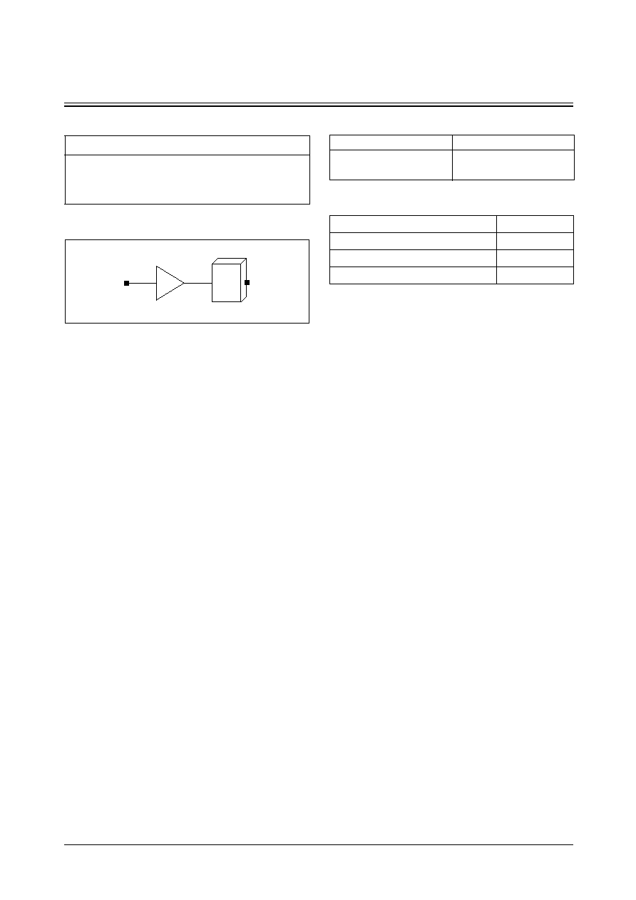
SEC ASIC
4-22
STDH90/MDL90
PHOByz
Normal Output Buffers
Cell Availability
Logic Symbol
5V Interface
PHOB(2/4/8/12/16/24)
PHOB(4/8/12/16/24)SM
PHOB(12/16/24)SH
PAD
A
Truth Table
Standard Load (SL)
A
PAD
0
0
1
1
Cell Name
A
PHOB(2/4/8/12/16/24)
5.7
PHOB(4/8/12/16/24)SM
5.7
PHOB(12/16/24)SH
5.7

STDH90/MDL90
4-23
SEC ASIC
PHOByz
Normal Output Buffers
PHOB2 Switching Characteristics
[Delays for typical process, 25 C, 5.0V, when t , t = 0.80ns]
o
R F
(CL : Capacitive Load[pf])
Path
Parameter
Delay [ns]
CL = 50.0pF
Delay Equations [ns]
Group1*
Group2*
Group3*
A to PAD
tR
21.432
0.832 + 0.412*CL
0.825 + 0.412*CL
0.816 + 0.412*CL
tF
18.562
0.742 + 0.356*CL
0.727 + 0.357*CL
0.733 + 0.357*CL
tPLH
10.778
1.288 + 0.190*CL
1.288 + 0.190*CL
1.288 + 0.190*CL
tPHL
10.577
1.303 + 0.185*CL
1.301 + 0.186*CL
1.299 + 0.186*CL
*Group1 : CL < 75, *Group2 : 75 CL 85, *Group3 : 85 < CL
< <
= =
PHOB4 Switching Characteristics
[Delays for typical process, 25 C, 5.0V, when t , t = 0.80ns]
o
R F
(CL : Capacitive Load[pf])
Path
Parameter
Delay [ns]
CL = 50.0pF
Delay Equations [ns]
Group1*
Group2*
Group3*
A to PAD
tR
10.735
0.433 + 0.206*CL
0.436 + 0.206*CL
0.430 + 0.206*CL
tF
9.310
0.398 + 0.178*CL
0.401 + 0.178*CL
0.395 + 0.178*CL
tPLH
5.904
1.160 + 0.095*CL
1.158 + 0.095*CL
1.156 + 0.095*CL
tPHL
5.894
1.254 + 0.093*CL
1.261 + 0.093*CL
1.259 + 0.093*CL
*Group1 : CL < 75, *Group2 : 75 CL 85, *Group3 : 85 < CL
< <
= =
PHOB4SM Switching Characteristics
[Delays for typical process, 25 C, 5.0V, when t , t = 0.80ns]
o
R F
(CL : Capacitive Load[pf])
Path
Parameter
Delay [ns]
CL = 50.0pF
Delay Equations [ns]
Group1*
Group2*
Group3*
A to PAD
tR
10.731
0.429 + 0.206*CL
0.424 + 0.206*CL
0.433 + 0.206*CL
tF
9.303
0.393 + 0.178*CL
0.393 + 0.178*CL
0.387 + 0.178*CL
tPLH
6.062
1.316 + 0.095*CL
1.317 + 0.095*CL
1.320 + 0.095*CL
tPHL
6.002
1.364 + 0.093*CL
1.361 + 0.093*CL
1.367 + 0.093*CL
*Group1 : CL < 75, *Group2 : 75 CL 85, *Group3 : 85 < CL
< <
= =
PHOB8 Switching Characteristics
[Delays for typical process, 25 C, 5.0V, when t , t = 0.80ns]
o
R F
(CL : Capacitive Load[pf])
Path
Parameter
Delay [ns]
CL = 50.0pF
Delay Equations [ns]
Group1*
Group2*
Group3*
A to PAD
tR
5.397
0.249 + 0.103*CL
0.239 + 0.103*CL
0.247 + 0.103*CL
tF
4.745
0.329 + 0.088*CL
0.300 + 0.089*CL
0.286 + 0.089*CL
tPLH
3.564
1.190 + 0.047*CL
1.196 + 0.047*CL
1.190 + 0.047*CL
tPHL
3.746
1.424 + 0.046*CL
1.427 + 0.046*CL
1.427 + 0.046*CL
*Group1 : CL < 75, *Group2 : 75 CL 85, *Group3 : 85 < CL
< <
= =
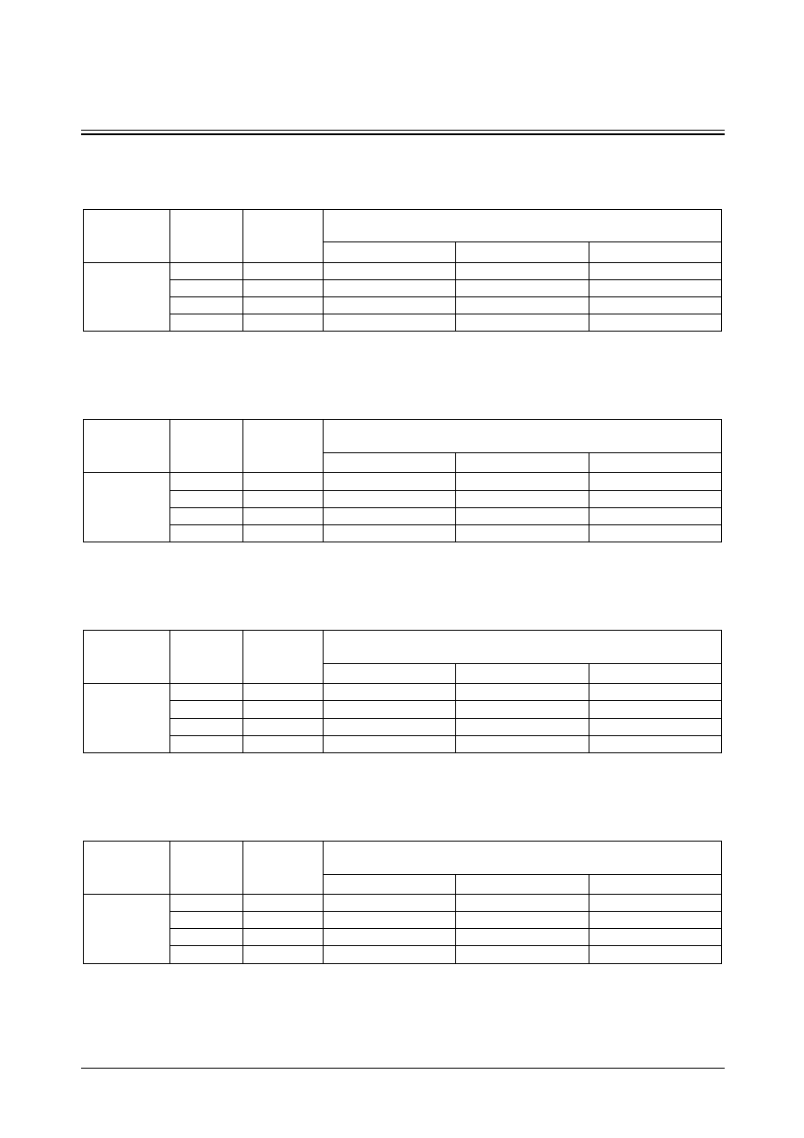
SEC ASIC
4-24
STDH90/MDL90
PHOByz
Normal Output Buffers
PHOB8SM Switching Characteristics
[Delays for typical process, 25 C, 5.0V, when t , t = 0.80ns]
o
R F
(CL : Capacitive Load[pf])
Path
Parameter
Delay [ns]
CL = 50.0pF
Delay Equations [ns]
Group1*
Group2*
Group3*
A to PAD
tR
5.390
0.240 + 0.103*CL
0.240 + 0.103*CL
0.240 + 0.103*CL
tF
4.726
0.306 + 0.088*CL
0.284 + 0.089*CL
0.269 + 0.089*CL
tPLH
3.687
1.315 + 0.047*CL
1.311 + 0.047*CL
1.313 + 0.047*CL
tPHL
3.785
1.465 + 0.046*CL
1.465 + 0.046*CL
1.465 + 0.046*CL
*Group1 : CL < 75, *Group2 : 75 CL 85, *Group3 : 85 < CL
< <
= =
PHOB12 Switching Characteristics
[Delays for typical process, 25 C, 5.0V, when t , t = 0.80ns]
o
R F
(CL : Capacitive Load[pf])
Path
Parameter
Delay [ns]
CL = 50.0pF
Delay Equations [ns]
Group1*
Group2*
Group3*
A to PAD
tR
3.640
0.224 + 0.068*CL
0.218 + 0.068*CL
0.201 + 0.069*CL
tF
3.319
0.429 + 0.058*CL
0.391 + 0.058*CL
0.377 + 0.058*CL
tPLH
2.868
1.286 + 0.032*CL
1.281 + 0.032*CL
1.284 + 0.032*CL
tPHL
3.198
1.636 + 0.031*CL
1.654 + 0.031*CL
1.654 + 0.031*CL
*Group1 : CL < 75, *Group2 : 75 CL 85, *Group3 : 85 < CL
< <
= =
PHOB12SM Switching Characteristics
[Delays for typical process, 25 C, 5.0V, when t , t = 0.80ns]
o
R F
(CL : Capacitive Load[pf])
Path
Parameter
Delay [ns]
CL = 50.0pF
Delay Equations [ns]
Group1*
Group2*
Group3*
A to PAD
tR
3.625
0.205 + 0.068*CL
0.190 + 0.069*CL
0.190 + 0.069*CL
tF
3.272
0.372 + 0.058*CL
0.334 + 0.059*CL
0.320 + 0.059*CL
tPLH
2.956
1.374 + 0.032*CL
1.377 + 0.032*CL
1.371 + 0.032*CL
tPHL
3.166
1.608 + 0.031*CL
1.628 + 0.031*CL
1.619 + 0.031*CL
*Group1 : CL < 75, *Group2 : 75 CL 85, *Group3 : 85 < CL
< <
= =
PHOB12SH Switching Characteristics
[Delays for typical process, 25 C, 5.0V, when t , t = 0.80ns]
o
R F
(CL : Capacitive Load[pf])
Path
Parameter
Delay [ns]
CL = 50.0pF
Delay Equations [ns]
Group1*
Group2*
Group3*
A to PAD
tR
3.651
0.251 + 0.068*CL
0.236 + 0.068*CL
0.219 + 0.068*CL
tF
3.344
0.464 + 0.058*CL
0.434 + 0.058*CL
0.417 + 0.058*CL
tPLH
3.503
1.917 + 0.032*CL
1.926 + 0.032*CL
1.920 + 0.032*CL
tPHL
3.563
1.987 + 0.032*CL
2.011 + 0.031*CL
2.022 + 0.031*CL
*Group1 : CL < 75, *Group2 : 75 CL 85, *Group3 : 85 < CL
< <
= =

STDH90/MDL90
4-25
SEC ASIC
PHOByz
Normal Output Buffers
PHOB16 Switching Characteristics
[Delays for typical process, 25 C, 5.0V, when t , t = 0.80ns]
o
R F
(CL : Capacitive Load[pf])
Path
Parameter
Delay [ns]
CL = 50.0pF
Delay Equations [ns]
Group1*
Group2*
Group3*
A to PAD
tR
2.794
0.262 + 0.051*CL
0.235 + 0.051*CL
0.224 + 0.051*CL
tF
2.682
0.550 + 0.043*CL
0.530 + 0.043*CL
0.511 + 0.043*CL
tPLH
2.582
1.392 + 0.024*CL
1.392 + 0.024*CL
1.398 + 0.024*CL
tPHL
3.023
1.813 + 0.024*CL
1.850 + 0.024*CL
1.865 + 0.024*CL
*Group1 : CL < 75, *Group2 : 75 CL 85, *Group3 : 85 < CL
< <
= =
PHOB16SM Switching Characteristics
[Delays for typical process, 25 C, 5.0V, when t , t = 0.80ns]
o
R F
(CL : Capacitive Load[pf])
Path
Parameter
Delay [ns]
CL = 50.0pF
Delay Equations [ns]
Group1*
Group2*
Group3*
A to PAD
tR
2.764
0.218 + 0.051*CL
0.205 + 0.051*CL
0.190 + 0.051*CL
tF
2.599
0.449 + 0.043*CL
0.441 + 0.043*CL
0.416 + 0.043*CL
tPLH
2.632
1.444 + 0.024*CL
1.441 + 0.024*CL
1.447 + 0.024*CL
tPHL
2.933
1.737 + 0.024*CL
1.761 + 0.024*CL
1.778 + 0.023*CL
*Group1 : CL < 75, *Group2 : 75 CL 85, *Group3 : 85 < CL
< <
= =
PHOB16SH Switching Characteristics
[Delays for typical process, 25 C, 5.0V, when t , t = 0.80ns]
o
R F
(CL : Capacitive Load[pf])
Path
Parameter
Delay [ns]
CL = 50.0pF
Delay Equations [ns]
Group1*
Group2*
Group3*
A to PAD
tR
2.781
0.247 + 0.051*CL
0.223 + 0.051*CL
0.217 + 0.051*CL
tF
2.634
0.496 + 0.043*CL
0.463 + 0.043*CL
0.457 + 0.043*CL
tPLH
3.140
1.948 + 0.024*CL
1.951 + 0.024*CL
1.957 + 0.024*CL
tPHL
3.237
2.021 + 0.024*CL
2.060 + 0.024*CL
2.083 + 0.024*CL
*Group1 : CL < 75, *Group2 : 75 CL 85, *Group3 : 85 < CL
< <
= =
PHOB24 Switching Characteristics
[Delays for typical process, 25 C, 5.0V, when t , t = 0.80ns]
o
R F
(CL : Capacitive Load[pf])
Path
Parameter
Delay [ns]
CL = 50.0pF
Delay Equations [ns]
Group1*
Group2*
Group3*
A to PAD
tR
2.024
0.382 + 0.033*CL
0.363 + 0.033*CL
0.337 + 0.033*CL
tF
2.159
0.733 + 0.029*CL
0.757 + 0.028*CL
0.757 + 0.028*CL
tPLH
2.406
1.590 + 0.016*CL
1.606 + 0.016*CL
1.621 + 0.016*CL
tPHL
2.993
2.073 + 0.018*CL
2.141 + 0.017*CL
2.189 + 0.017*CL
*Group1 : CL < 75, *Group2 : 75 CL 85, *Group3 : 85 < CL
< <
= =
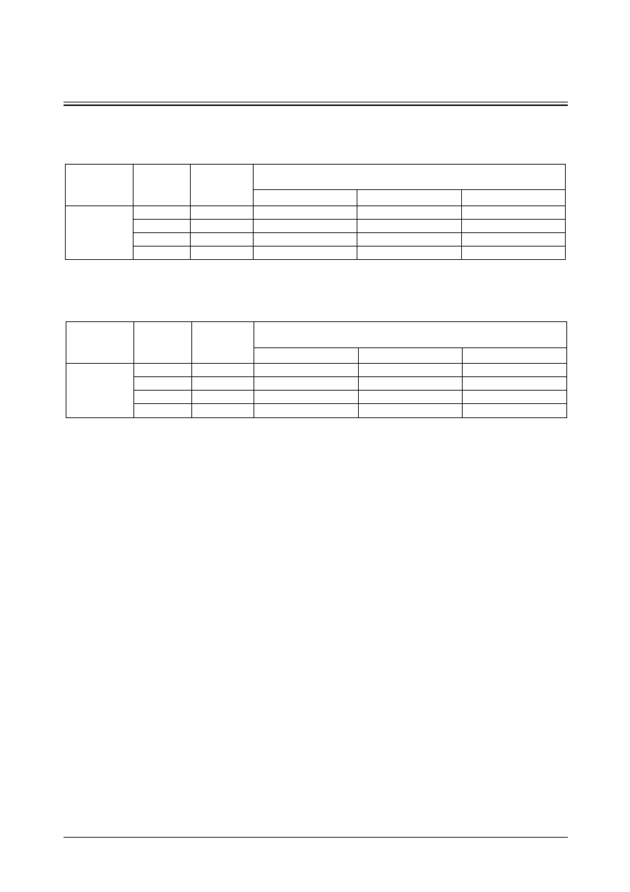
SEC ASIC
4-26
STDH90/MDL90
PHOByz
Normal Output Buffers
PHOB24SM Switching Characteristics
[Delays for typical process, 25 C, 5.0V, when t , t = 0.80ns]
o
R F
(CL : Capacitive Load[pf])
Path
Parameter
Delay [ns]
CL = 50.0pF
Delay Equations [ns]
Group1*
Group2*
Group3*
A to PAD
tR
1.953
0.291 + 0.033*CL
0.271 + 0.034*CL
0.263 + 0.034*CL
tF
2.024
0.610 + 0.028*CL
0.609 + 0.028*CL
0.606 + 0.028*CL
tPLH
2.385
1.579 + 0.016*CL
1.595 + 0.016*CL
1.593 + 0.016*CL
tPHL
2.811
1.927 + 0.018*CL
1.993 + 0.017*CL
2.016 + 0.017*CL
*Group1 : CL < 75, *Group2 : 75 CL 85, *Group3 : 85 < CL
< <
= =
PHOB24SH Switching Characteristics
[Delays for typical process, 25 C, 5.0V, when t , t = 0.80ns]
o
R F
(CL : Capacitive Load[pf])
Path
Parameter
Delay [ns]
CL = 50.0pF
Delay Equations [ns]
Group1*
Group2*
Group3*
A to PAD
tR
1.963
0.307 + 0.033*CL
0.271 + 0.034*CL
0.277 + 0.034*CL
tF
2.019
0.591 + 0.029*CL
0.596 + 0.028*CL
0.604 + 0.028*CL
tPLH
2.863
2.051 + 0.016*CL
2.069 + 0.016*CL
2.075 + 0.016*CL
tPHL
3.040
2.144 + 0.018*CL
2.213 + 0.017*CL
2.236 + 0.017*CL
*Group1 : CL < 75, *Group2 : 75 CL 85, *Group3 : 85 < CL
< <
= =
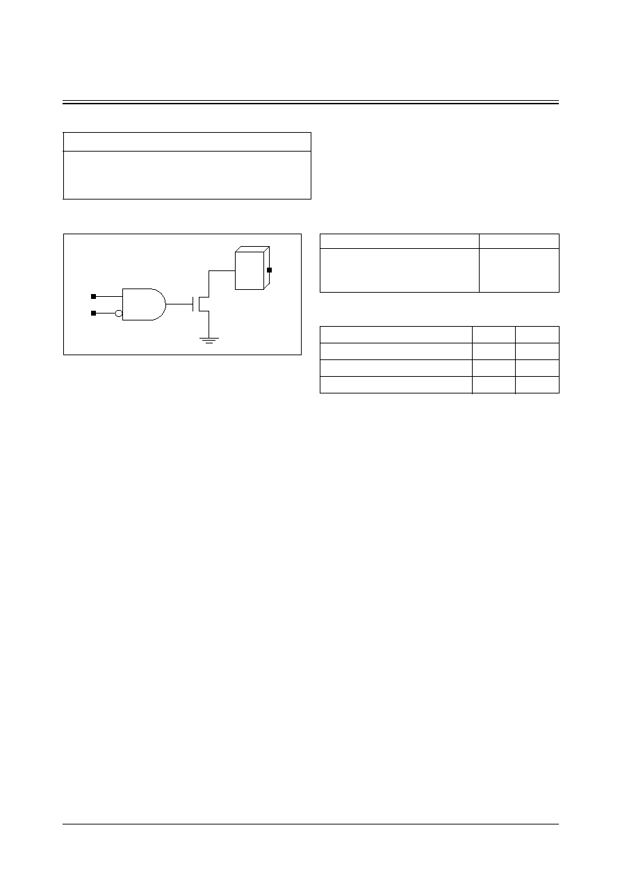
STDH90/MDL90
4-27
SEC ASIC
PHODyz
Open Drain Output Buffers
Cell Availability
Logic Symbol
5V Interface
PHOD(2/4/8/12/16/24)
PHOD(4/8/12/16/24)SM
PHOD(12/16/24)SH
PAD
TN
EN
Truth Table
Standard Load (SL)
TN
EN
PAD
1
0
0
0
x
Hi-Z
x
1
Hi-Z
Cell Name
TN
EN
PHOD(2/4/8/12/16//24)
2.1
2.4
PHOD(4/8/12/16/24)SM
2.1
2.4
PHOD(12/16/24)SH
2.1
2.4
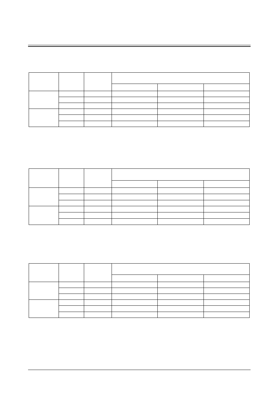
SEC ASIC
4-28
STDH90/MDL90
PHODyz
Open Drain Output Buffers
PHOD2 Switching Characteristics
[Delays for typical process, 25 C, 5.0V, when t , t = 0.80ns]
o
R F
(CL : Capacitive Load[pf])
Path
Parameter
Delay [ns]
CL = 50.0pF
Delay Equations [ns]
Group1*
Group2*
Group3*
TN to PAD
tF
18.352
0.530 + 0.356*CL
0.526 + 0.356*CL
0.523 + 0.357*CL
tPHL
10.521
1.245 + 0.186*CL
1.239 + 0.186*CL
1.250 + 0.185*CL
tPLZ
1.192
1.192 + 0.000*CL
1.192 + 0.000*CL
1.192 + 0.000*CL
EN to PAD
tF
18.351
0.527 + 0.356*CL
0.526 + 0.356*CL
0.517 + 0.357*CL
tPHL
10.817
1.541 + 0.186*CL
1.543 + 0.185*CL
1.545 + 0.185*CL
tPLZ
0.893
0.893 + 0.000*CL
0.893 + 0.000*CL
0.893 + 0.000*CL
*Group1 : CL < 75, *Group2 : 75 CL 85, *Group3 : 85 < CL
< <
= =
PHOD4 Switching Characteristics
[Delays for typical process, 25 C, 5.0V, when t , t = 0.80ns]
o
R F
(CL : Capacitive Load[pf])
Path
Parameter
Delay [ns]
CL = 50.0pF
Delay Equations [ns]
Group1*
Group2*
Group3*
TN to PAD
tF
9.205
0.293 + 0.178*CL
0.296 + 0.178*CL
0.290 + 0.178*CL
tPHL
5.902
1.264 + 0.093*CL
1.254 + 0.093*CL
1.268 + 0.093*CL
tPLZ
1.253
1.253 + 0.000*CL
1.253 + 0.000*CL
1.253 + 0.000*CL
EN to PAD
tF
9.205
0.293 + 0.178*CL
0.296 + 0.178*CL
0.290 + 0.178*CL
tPHL
6.197
1.559 + 0.093*CL
1.556 + 0.093*CL
1.562 + 0.093*CL
tPLZ
0.946
0.946 + 0.000*CL
0.946 + 0.000*CL
0.946 + 0.000*CL
*Group1 : CL < 75, *Group2 : 75 CL 85, *Group3 : 85 < CL
< <
= =
PHOD4SM Switching Characteristics
[Delays for typical process, 25 C, 5.0V, when t , t = 0.80ns]
o
R F
(CL : Capacitive Load[pf])
Path
Parameter
Delay [ns]
CL = 50.0pF
Delay Equations [ns]
Group1*
Group2*
Group3*
TN to PAD
tF
9.198
0.288 + 0.178*CL
0.288 + 0.178*CL
0.282 + 0.178*CL
tPHL
5.999
1.361 + 0.093*CL
1.358 + 0.093*CL
1.364 + 0.093*CL
tPLZ
1.329
1.329 + 0.000*CL
1.329 + 0.000*CL
1.329 + 0.000*CL
EN to PAD
tF
9.198
0.288 + 0.178*CL
0.288 + 0.178*CL
0.282 + 0.178*CL
tPHL
6.294
1.656 + 0.093*CL
1.653 + 0.093*CL
1.659 + 0.093*CL
tPLZ
0.993
0.993 + 0.000*CL
0.993 + 0.000*CL
0.993 + 0.000*CL
*Group1 : CL < 75, *Group2 : 75 CL 85, *Group3 : 85 < CL
< <
= =
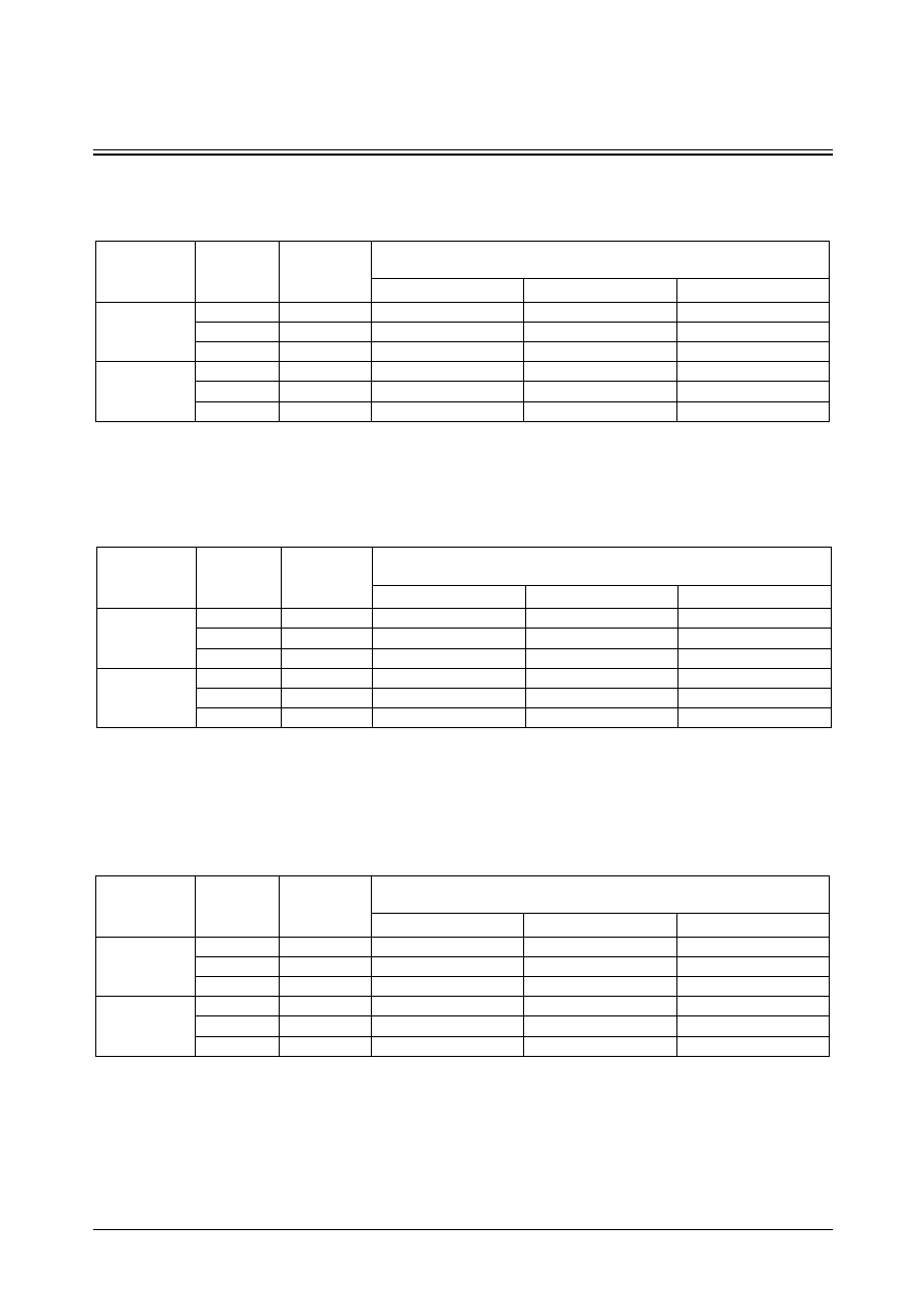
STDH90/MDL90
4-29
SEC ASIC
PHODyz
Open Drain Output Buffers
PHOD8 Switching Characteristics
[Delays for typical process, 25 C, 5.0V, when t , t = 0.80ns]
o
R F
(CL : Capacitive Load[pf])
Path
Parameter
Delay [ns]
CL = 50.0pF
Delay Equations [ns]
Group1*
Group2*
Group3*
TN to PAD
tF
4.694
0.278 + 0.088*CL
0.250 + 0.089*CL
0.241 + 0.089*CL
tPHL
3.789
1.469 + 0.046*CL
1.469 + 0.046*CL
1.469 + 0.046*CL
tPLZ
1.307
1.307 + 0.000*CL
1.307 + 0.000*CL
1.307 + 0.000*CL
EN to PAD
tF
4.695
0.281 + 0.088*CL
0.250 + 0.089*CL
0.241 + 0.089*CL
tPHL
4.084
1.764 + 0.046*CL
1.764 + 0.046*CL
1.764 + 0.046*CL
tPLZ
0.988
0.988 + 0.000*CL
0.988 + 0.000*CL
0.988 + 0.000*CL
*Group1 : CL < 75, *Group2 : 75 CL 85, *Group3 : 85 < CL
< <
= =
PHOD8SM Switching Characteristics
[Delays for typical process, 25 C, 5.0V, when t , t = 0.80ns]
o
R F
(CL : Capacitive Load[pf])
Path
Parameter
Delay [ns]
CL = 50.0pF
Delay Equations [ns]
Group1*
Group2*
Group3*
TN to PAD
tF
4.676
0.258 + 0.088*CL
0.233 + 0.089*CL
0.224 + 0.089*CL
tPHL
3.815
1.495 + 0.046*CL
1.495 + 0.046*CL
1.495 + 0.046*CL
tPLZ
1.376
1.376 + 0.000*CL
1.346 + 0.000*CL
1.346 + 0.000*CL
EN to PAD
tF
4.677
0.261 + 0.088*CL
0.233 + 0.089*CL
0.224 + 0.089*CL
tPHL
4.110
1.790 + 0.046*CL
1.790 + 0.046*CL
1.790 + 0.046*CL
tPLZ
1.034
1.034 + 0.000*CL
1.034 + 0.000*CL
1.034 + 0.000*CL
*Group1 : CL < 75, *Group2 : 75 CL 85, *Group3 : 85 < CL
< <
= =
PHOD12 Switching Characteristics
[Delays for typical process, 25 C, 5.0V, when t , t = 0.80ns]
o
R F
(CL : Capacitive Load[pf])
Path
Parameter
Delay [ns]
CL = 50.0pF
Delay Equations [ns]
Group1*
Group2*
Group3*
TN to PAD
tF
3.290
0.404 + 0.058*CL
0.368 + 0.058*CL
0.345 + 0.058*CL
tPHL
3.248
1.686 + 0.031*CL
1.704 + 0.031*CL
1.704 + 0.031*CL
tPLZ
1.349
1.349 + 0.000*CL
1.349 + 0.000*CL
1.349 + 0.000*CL
EN to PAD
tF
3.291
0.405 + 0.058*CL
0.376 + 0.058*CL
0.351 + 0.058*CL
tPHL
3.543
1.983 + 0.031*CL
1.990 + 0.031*CL
2.005 + 0.031*CL
tPLZ
1.043
1.043 + 0.000*CL
1.043 + 0.000*CL
1.043 + 0.000*CL
*Group1 : CL < 75, *Group2 : 75 CL 85, *Group3 : 85 < CL
< <
= =

SEC ASIC
4-30
STDH90/MDL90
PHODyz
Open Drain Output Buffers
PHOD12SM Switching Characteristics
[Delays for typical process, 25 C, 5.0V, when t , t = 0.80ns]
o
R F
(CL : Capacitive Load[pf])
Path
Parameter
Delay [ns]
CL = 50.0pF
Delay Equations [ns]
Group1*
Group2*
Group3*
TN to PAD
tF
3.243
0.345 + 0.058*CL
0.312 + 0.058*CL
0.301 + 0.059*CL
tPHL
3.208
1.652 + 0.031*CL
1.661 + 0.031*CL
1.667 + 0.031*CL
tPLZ
1.402
1.402 + 0.000*CL
1.402 + 0.000*CL
1.402 + 0.000*CL
EN to PAD
tF
3.243
0.345 + 0.058*CL
0.312 + 0.058*CL
0.301 + 0.059*CL
tPHL
3.501
1.945 + 0.031*CL
1.954 + 0.031*CL
1.960 + 0.031*CL
tPLZ
1.079
1.079 + 0.000*CL
1.079 + 0.000*CL
1.079 + 0.000*CL
*Group1 : CL < 75, *Group2 : 75 CL 85, *Group3 : 85 < CL
< <
= =
PHOD12SH Switching Characteristics
[Delays for typical process, 25 C, 5.0V, when t , t = 0.80ns]
o
R F
(CL : Capacitive Load[pf])
Path
Parameter
Delay [ns]
CL = 50.0pF
Delay Equations [ns]
Group1*
Group2*
Group3*
TN to PAD
tF
3.301
0.419 + 0.058*CL
0.392 + 0.058*CL
0.369 + 0.058*CL
tPHL
3.526
1.952 + 0.031*CL
1.981 + 0.031*CL
1.983 + 0.031*CL
tPLZ
1.592
1.592 + 0.000*CL
1.592 + 0.000*CL
1.592 + 0.000*CL
EN to PAD
tF
3.302
0.422 + 0.058*CL
0.392 + 0.058*CL
0.369 + 0.058*CL
tPHL
3.819
2.245 + 0.031*CL
2.273 + 0.031*CL
2.276 + 0.031*CL
tPLZ
1.296
1.296 + 0.000*CL
1.296 + 0.000*CL
1.296 + 0.000*CL
*Group1 : CL < 75, *Group2 : 75 CL 85, *Group3 : 85 < CL
< <
= =
PHOD16 Switching Characteristics
[Delays for typical process, 25 C, 5.0V, when t , t = 0.80ns]
o
R F
(CL : Capacitive Load[pf])
Path
Parameter
Delay [ns]
CL = 50.0pF
Delay Equations [ns]
Group1*
Group2*
Group3*
TN to PAD
tF
2.667
0.541 + 0.043*CL
0.520 + 0.043*CL
0.497 + 0.043*CL
tPHL
3.076
1.864 + 0.024*CL
1.904 + 0.024*CL
1.919 + 0.024*CL
tPLZ
1.409
1.409 + 0.000*CL
1.409 + 0.000*CL
1.409 + 0.000*CL
EN to PAD
tF
2.668
0.544 + 0.042*CL
0.520 + 0.043*CL
0.497 + 0.043*CL
tPHL
3.371
2.157 + 0.024*CL
2.200 + 0.024*CL
2.215 + 0.024*CL
tPLZ
1.098
1.098 + 0.000*CL
1.098 + 0.000*CL
1.098 + 0.000*CL
*Group1 : CL < 75, *Group2 : 75 CL 85, *Group3 : 85 < CL
< <
= =
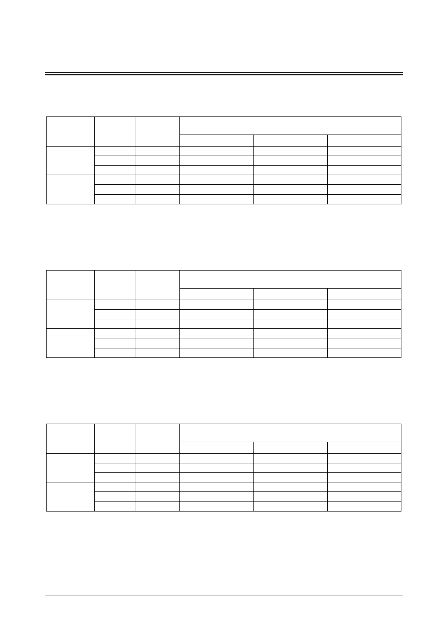
STDH90/MDL90
4-31
SEC ASIC
PHODyz
Open Drain Output Buffers
PHOD16SM Switching Characteristics
[Delays for typical process, 25 C, 5.0V, when t , t = 0.80ns]
o
R F
(CL : Capacitive Load[pf])
Path
Parameter
Delay [ns]
CL = 50.0pF
Delay Equations [ns]
Group1*
Group2*
Group3*
TN to PAD
tF
2.583
0.441 + 0.043*CL
0.421 + 0.043*CL
0.402 + 0.043*CL
tPHL
2.980
1.784 + 0.024*CL
1.808 + 0.024*CL
1.825 + 0.023*CL
tPLZ
1.427
1.427 + 0.000*CL
1.427 + 0.000*CL
1.427 + 0.000*CL
EN to PAD
tF
2.584
0.444 + 0.043*CL
0.421 + 0.043*CL
0.402 + 0.043*CL
tPHL
3.273
2.077 + 0.024*CL
2.101 + 0.024*CL
2.118 + 0.023*CL
tPLZ
1.116
1.116 + 0.000*CL
1.116 + 0.000*CL
1.116 + 0.000*CL
*Group1 : CL < 75, *Group2 : 75 CL 85, *Group3 : 85 < CL
< <
= =
PHOD16SH Switching Characteristics
[Delays for typical process, 25 C, 5.0V, when t , t = 0.80ns]
o
R F
(CL : Capacitive Load[pf])
Path
Parameter
Delay [ns]
CL = 50.0pF
Delay Equations [ns]
Group1*
Group2*
Group3*
TN to PAD
tF
2.602
0.466 + 0.043*CL
0.437 + 0.043*CL
0.423 + 0.043*CL
tPHL
3.209
1.999 + 0.024*CL
2.036 + 0.024*CL
2.051 + 0.024*CL
tPLZ
1.664
1.664 + 0.000*CL
1.664 + 0.000*CL
1.664 + 0.000*CL
EN to PAD
tF
2.602
0.466 + 0.043*CL
0.437 + 0.043*CL
0.423 + 0.043*CL
tPHL
3.502
2.292 + 0.024*CL
2.329 + 0.024*CL
2.344 + 0.024*CL
tPLZ
1.358
1.358 + 0.000*CL
1.358 + 0.000*CL
1.358 + 0.000*CL
*Group1 : CL < 75, *Group2 : 75 CL 85, *Group3 : 85 < CL
< <
= =
PHOD24 Switching Characteristics
[Delays for typical process, 25 C, 5.0V, when t , t = 0.80ns]
o
R F
(CL : Capacitive Load[pf])
Path
Parameter
Delay [ns]
CL = 50.0pF
Delay Equations [ns]
Group1*
Group2*
Group3*
TN to PAD
tF
2.165
0.755 + 0.028*CL
0.763 + 0.028*CL
0.760 + 0.028*CL
tPHL
3.046
2.120 + 0.019*CL
2.197 + 0.017*CL
2.239 + 0.017*CL
tPLZ
1.513
1.513 + 0.000*CL
1.513 + 0.000*CL
1.513 + 0.000*CL
EN to PAD
tF
2.165
0.755 + 0.028*CL
0.763 + 0.028*CL
0.760 + 0.028*CL
tPHL
3.341
2.415 + 0.019*CL
2.491 + 0.018*CL
2.534 + 0.017*CL
tPLZ
1.205
1.205 + 0.000*CL
1.205 + 0.000*CL
1.205 + 0.000*CL
*Group1 : CL < 75, *Group2 : 75 CL 85, *Group3 : 85 < CL
< <
= =
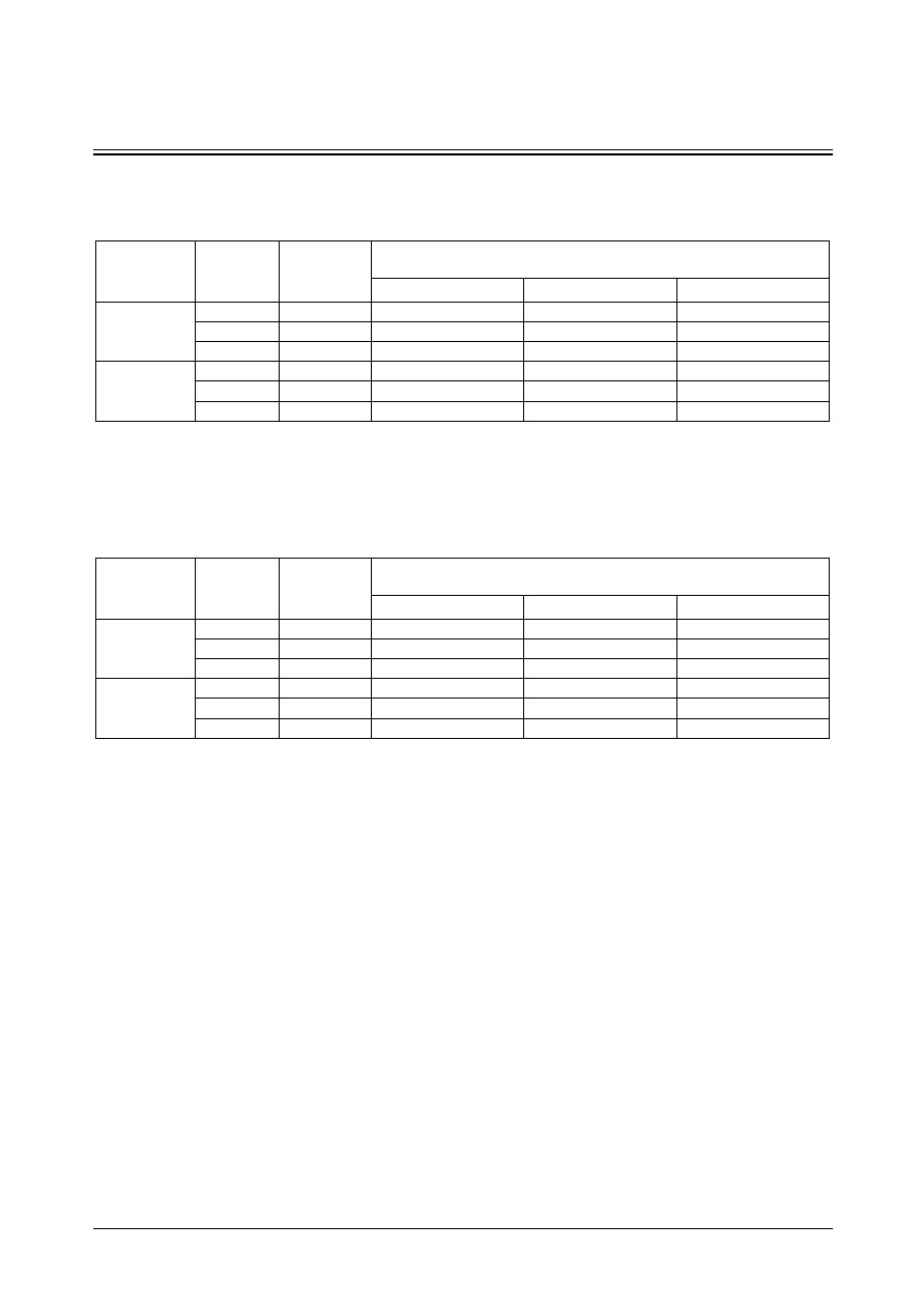
SEC ASIC
4-32
STDH90/MDL90
PHODyz
Open Drain Output Buffers
PHOD24SM Switching Characteristics
[Delays for typical process, 25 C, 5.0V, when t , t = 0.80ns]
o
R F
(CL : Capacitive Load[pf])
Path
Parameter
Delay [ns]
CL = 50.0pF
Delay Equations [ns]
Group1*
Group2*
Group3*
TN to PAD
tF
2.020
0.608 + 0.028*CL
0.611 + 0.028*CL
0.611 + 0.028*CL
tPHL
2.863
1.977 + 0.018*CL
2.038 + 0.017*CL
2.070 + 0.017*CL
tPLZ
1.497
1.497 + 0.000*CL
1.497 + 0.000*CL
1.497 + 0.000*CL
EN to PAD
tF
2.020
0.608 + 0.028*CL
0.619 + 0.028*CL
0.604 + 0.028*CL
tPHL
3.157
2.271 + 0.018*CL
2.332 + 0.017*CL
2.364 + 0.017*CL
tPLZ
1.187
1.187 + 0.000*CL
1.187 + 0.000*CL
1.187 + 0.000*CL
*Group1 : CL < 75, *Group2 : 75 CL 85, *Group3 : 85 < CL
< <
= =
PHOD24SH Switching Characteristics
[Delays for typical process, 25 C, 5.0V, when t , t = 0.80ns]
o
R F
(CL : Capacitive Load[pf])
Path
Parameter
Delay [ns]
CL = 50.0pF
Delay Equations [ns]
Group1*
Group2*
Group3*
TN to PAD
tF
2.001
0.577 + 0.028*CL
0.598 + 0.028*CL
0.581 + 0.028*CL
tPHL
3.023
2.133 + 0.018*CL
2.193 + 0.017*CL
2.227 + 0.017*CL
tPLZ
1.717
1.717 + 0.000*CL
1.717 + 0.000*CL
1.717 + 0.000*CL
EN to PAD
tF
2.002
0.582 + 0.028*CL
0.582 + 0.028*CL
0.593 + 0.028*CL
tPHL
3.316
2.426 + 0.018*CL
2.486 + 0.017*CL
2.520 + 0.017*CL
tPLZ
1.420
1.420 + 0.000*CL
1.420 + 0.000*CL
1.420 + 0.000*CL
*Group1 : CL < 75, *Group2 : 75 CL 85, *Group3 : 85 < CL
< <
= =
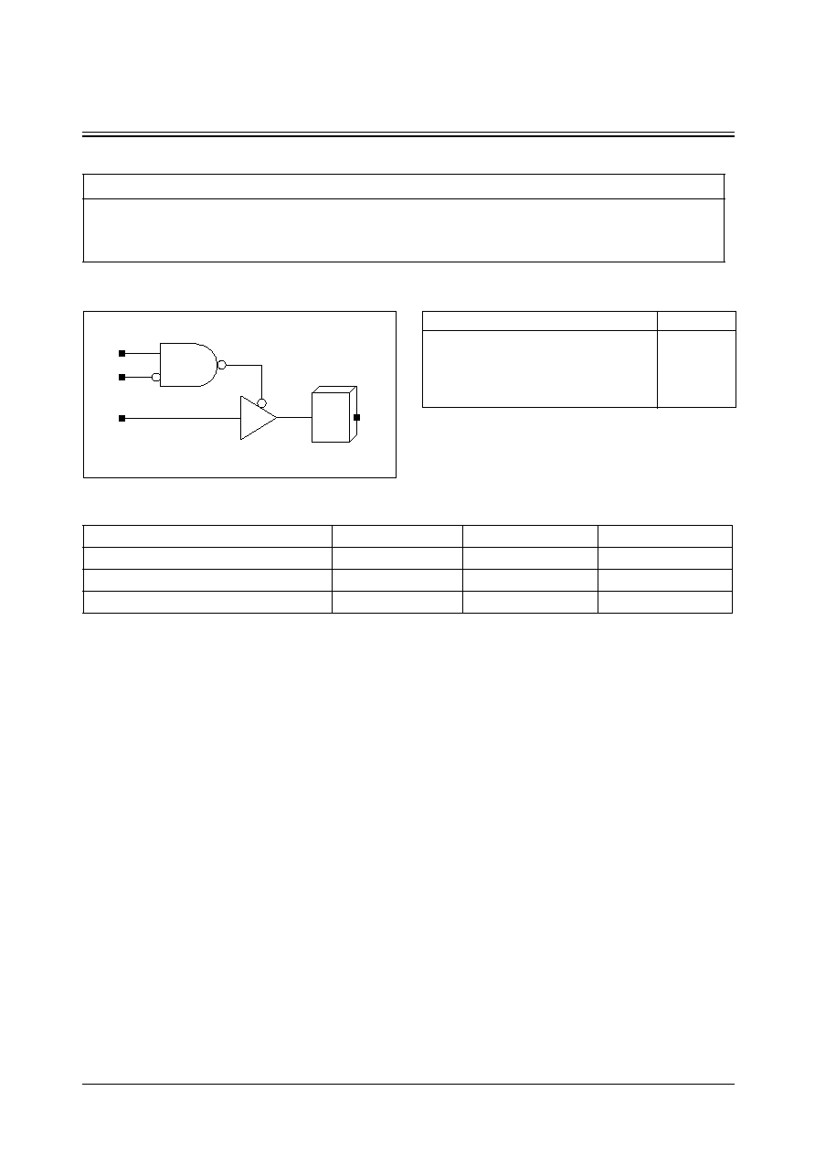
STDH90/MDL90
4-33
SEC ASIC
PHOTyz
Tri-State Output Buffers
Cell Availability
Logic Symbol
Standard Load (SL)
5V Interface
PHOT(2/4/8/12/16//24)
PHOT(4/8/12/16/24)SM
PHOT(12/16/24)SH
Cell Name
TN
EN
A
PHOT(2/4/8/12/16/24)
2.1
2.4
5.7
PHOT(4/8/12/16/24)SM
2.1
2.4
5.7
PHOT(12/16/24)SH
2.1
2.4
5.7
PAD
A
TN
EN
Truth Table
TN
EN
A
PAD
1
0
0
0
1
0
1
1
x
1
x
Hi-Z
0
x
x
Hi-Z

SEC ASIC
4-34
STDH90/MDL90
PHOTyz
Tri-State Output Buffers
PHOT2 Switching Characteristics
[Delays for typical process, 25 C, 5.0V, when t , t = 0.80ns]
o
R F
(CL : Capacitive Load[pf])
Path
Parameter
Delay [ns]
CL = 50.0pF
Delay Equations [ns]
Group1*
Group2*
Group3*
A to PAD
tR
21.431
0.829 + 0.412*CL
0.825 + 0.412*CL
0.816 + 0.412*CL
tF
18.562
0.742 + 0.356*CL
0.727 + 0.357*CL
0.733 + 0.357*CL
tPLH
10.900
1.410 + 0.190*CL
1.410 + 0.190*CL
1.410 + 0.190*CL
tPHL
10.624
1.348 + 0.186*CL
1.349 + 0.186*CL
1.352 + 0.185*CL
TN to PAD
tR
21.432
0.832 + 0.412*CL
0.825 + 0.412*CL
0.816 + 0.412*CL
tF
18.562
0.742 + 0.356*CL
0.727 + 0.357*CL
0.733 + 0.357*CL
tPLH
10.931
1.439 + 0.190*CL
1.434 + 0.190*CL
1.443 + 0.190*CL
tPHL
10.771
1.497 + 0.185*CL
1.488 + 0.186*CL
1.494 + 0.186*CL
tPLZ
1.329
1.329 + 0.000*CL
1.329 + 0.000*CL
1.329 + 0.000*CL
tPHZ
1.311
1.311 + 0.000*CL
1.311 + 0.000*CL
1.311 + 0.000*CL
EN to PAD
tR
21.432
0.832 + 0.412*CL
0.825 + 0.412*CL
0.816 + 0.412*CL
tF
18.562
0.742 + 0.356*CL
0.727 + 0.357*CL
0.733 + 0.357*CL
tPLH
11.214
1.722 + 0.190*CL
1.725 + 0.190*CL
1.702 + 0.190*CL
tPHL
11.064
1.788 + 0.186*CL
1.790 + 0.185*CL
1.792 + 0.185*CL
tPLZ
1.015
1.015 + 0.000*CL
1.015 + 0.000*CL
1.015 + 0.000*CL
tPHZ
1.006
1.006 + 0.000*CL
1.006 + 0.000*CL
1.006 + 0.000*CL
*Group1 : CL < 75, *Group2 : 75 CL 85, *Group3 : 85 < CL
< <
= =
PHOT4 Switching Characteristics
[Delays for typical process, 25 C, 5.0V, when t , t = 0.80ns]
o
R F
(CL : Capacitive Load[pf])
Path
Parameter
Delay [ns]
CL = 50.0pF
Delay Equations [ns]
Group1*
Group2*
Group3*
A to PAD
tR
10.735
0.433 + 0.206*CL
0.436 + 0.206*CL
0.430 + 0.206*CL
tF
9.310
0.398 + 0.178*CL
0.401 + 0.178*CL
0.395 + 0.178*CL
tPLH
6.028
1.282 + 0.095*CL
1.268 + 0.095*CL
1.294 + 0.095*CL
tPHL
5.941
1.303 + 0.093*CL
1.307 + 0.093*CL
1.299 + 0.093*CL
TN to PAD
tR
10.734
0.430 + 0.206*CL
0.436 + 0.206*CL
0.430 + 0.206*CL
tF
9.310
0.398 + 0.178*CL
0.401 + 0.178*CL
0.395 + 0.178*CL
tPLH
6.063
1.317 + 0.095*CL
1.311 + 0.095*CL
1.322 + 0.095*CL
tPHL
6.087
1.449 + 0.093*CL
1.446 + 0.093*CL
1.452 + 0.093*CL
tPLZ
1.385
1.385 + 0.000*CL
1.385 + 0.000*CL
1.385 + 0.000*CL
tPHZ
1.407
1.407 + 0.000*CL
1.407 + 0.000*CL
1.407 + 0.000*CL
EN to PAD
tR
10.735
0.433 + 0.206*CL
0.436 + 0.206*CL
0.430 + 0.206*CL
tF
9.310
0.398 + 0.178*CL
0.401 + 0.178*CL
0.395 + 0.178*CL
tPLH
6.345
1.599 + 0.095*CL
1.600 + 0.095*CL
1.581 + 0.095*CL
tPHL
6.378
1.740 + 0.093*CL
1.737 + 0.093*CL
1.743 + 0.093*CL
tPLZ
1.064
1.064 + 0.000*CL
1.064 + 0.000*CL
1.064 + 0.000*CL
tPHZ
1.103
1.103 + 0.000*CL
1.100 + 0.000*CL
1.100 + 0.000*CL
*Group1 : CL < 75, *Group2 : 75 CL 85, *Group3 : 85 < CL
< <
= =

STDH90/MDL90
4-35
SEC ASIC
PHOTyz
Tri-State Output Buffers
PHOT4SM Switching Characteristics
[Delays for typical process, 25 C, 5.0V, when t , t = 0.80ns]
o
R F
(CL : Capacitive Load[pf])
Path
Parameter
Delay [ns]
CL = 50.0pF
Delay Equations [ns]
Group1*
Group2*
Group3*
A to PAD
tR
10.731
0.429 + 0.206*CL
0.424 + 0.206*CL
0.433 + 0.206*CL
tF
9.303
0.393 + 0.178*CL
0.393 + 0.178*CL
0.387 + 0.178*CL
tPLH
6.274
1.528 + 0.095*CL
1.530 + 0.095*CL
1.532 + 0.095*CL
tPHL
6.072
1.434 + 0.093*CL
1.431 + 0.093*CL
1.437 + 0.093*CL
TN to PAD
tR
10.731
0.429 + 0.206*CL
0.424 + 0.206*CL
0.433 + 0.206*CL
tF
9.303
0.393 + 0.178*CL
0.393 + 0.178*CL
0.387 + 0.178*CL
tPLH
6.284
1.538 + 0.095*CL
1.540 + 0.095*CL
1.542 + 0.095*CL
tPHL
6.205
1.567 + 0.093*CL
1.564 + 0.093*CL
1.564 + 0.093*CL
tPLZ
1.432
1.432 + 0.000*CL
1.432 + 0.000*CL
1.432 + 0.000*CL
tPHZ
1.400
1.400 + 0.000*CL
1.400 + 0.000*CL
1.400 + 0.000*CL
EN to PAD
tR
10.731
0.429 + 0.206*CL
0.424 + 0.206*CL
0.433 + 0.206*CL
tF
9.303
0.393 + 0.178*CL
0.393 + 0.178*CL
0.387 + 0.178*CL
tPLH
6.566
1.820 + 0.095*CL
1.836 + 0.095*CL
1.811 + 0.095*CL
tPHL
6.499
1.861 + 0.093*CL
1.858 + 0.093*CL
1.864 + 0.093*CL
tPLZ
1.131
1.131 + 0.000*CL
1.131 + 0.000*CL
1.131 + 0.000*CL
tPHZ
1.092
1.092 + 0.000*CL
1.092 + 0.000*CL
1.092 + 0.000*CL
*Group1 : CL < 75, *Group2 : 75 CL 85, *Group3 : 85 < CL
< <
= =
PHOT8 Switching Characteristics
[Delays for typical process, 25 C, 5.0V, when t , t = 0.80ns]
o
R F
(CL : Capacitive Load[pf])
Path
Parameter
Delay [ns]
CL = 50.0pF
Delay Equations [ns]
Group1*
Group2*
Group3*
A to PAD
tR
5.397
0.249 + 0.103*CL
0.246 + 0.103*CL
0.240 + 0.103*CL
tF
4.745
0.327 + 0.088*CL
0.309 + 0.089*CL
0.286 + 0.089*CL
tPLH
3.700
1.328 + 0.047*CL
1.324 + 0.047*CL
1.326 + 0.047*CL
tPHL
3.790
1.468 + 0.046*CL
1.471 + 0.046*CL
1.471 + 0.046*CL
TN to PAD
tR
5.397
0.249 + 0.103*CL
0.239 + 0.103*CL
0.247 + 0.103*CL
tF
4.744
0.324 + 0.088*CL
0.309 + 0.089*CL
0.286 + 0.089*CL
tPLH
3.726
1.352 + 0.047*CL
1.351 + 0.047*CL
1.353 + 0.047*CL
tPHL
3.936
1.616 + 0.046*CL
1.601 + 0.047*CL
1.624 + 0.046*CL
tPLZ
1.436
1.436 + 0.000*CL
1.421 + 0.000*CL
1.438 + 0.000*CL
tPHZ
1.598
1.598 + 0.000*CL
1.595 + 0.000*CL
1.595 + 0.000*CL
EN to PAD
tR
5.397
0.249 + 0.103*CL
0.239 + 0.103*CL
0.247 + 0.103*CL
tF
4.745
0.329 + 0.088*CL
0.300 + 0.089*CL
0.286 + 0.089*CL
tPLH
4.016
1.642 + 0.047*CL
1.640 + 0.048*CL
1.649 + 0.047*CL
tPHL
4.227
1.907 + 0.046*CL
1.907 + 0.046*CL
1.907 + 0.046*CL
tPLZ
1.129
1.129 + 0.000*CL
1.129 + 0.000*CL
1.129 + 0.000*CL
tPHZ
1.290
1.290 + 0.000*CL
1.290 + 0.000*CL
1.290 + 0.000*CL
*Group1 : CL < 75, *Group2 : 75 CL 85, *Group3 : 85 < CL
< <
= =

SEC ASIC
4-36
STDH90/MDL90
PHOTyz
Tri-State Output Buffers
PHOT8SM Switching Characteristics
[Delays for typical process, 25 C, 5.0V, when t , t = 0.80ns]
o
R F
(CL : Capacitive Load[pf])
Path
Parameter
Delay [ns]
CL = 50.0pF
Delay Equations [ns]
Group1*
Group2*
Group3*
A to PAD
tR
5.391
0.243 + 0.103*CL
0.240 + 0.103*CL
0.240 + 0.103*CL
tF
4.727
0.309 + 0.088*CL
0.284 + 0.089*CL
0.269 + 0.089*CL
tPLH
3.908
1.534 + 0.047*CL
1.540 + 0.047*CL
1.534 + 0.047*CL
tPHL
3.861
1.539 + 0.046*CL
1.542 + 0.046*CL
1.548 + 0.046*CL
TN to PAD
tR
5.391
0.243 + 0.103*CL
0.240 + 0.103*CL
0.240 + 0.103*CL
tF
4.726
0.304 + 0.088*CL
0.284 + 0.089*CL
0.276 + 0.089*CL
tPLH
3.908
1.536 + 0.047*CL
1.532 + 0.047*CL
1.534 + 0.047*CL
tPHL
3.983
1.663 + 0.046*CL
1.640 + 0.047*CL
1.666 + 0.046*CL
tPLZ
1.471
1.471 + 0.000*CL
1.471 + 0.000*CL
1.471 + 0.000*CL
tPHZ
1.498
1.498 + 0.000*CL
1.498 + 0.000*CL
1.498 + 0.000*CL
EN to PAD
tR
5.391
0.243 + 0.103*CL
0.240 + 0.103*CL
0.240 + 0.103*CL
tF
4.727
0.309 + 0.088*CL
0.284 + 0.089*CL
0.269 + 0.089*CL
tPLH
4.196
1.824 + 0.047*CL
1.834 + 0.047*CL
1.809 + 0.048*CL
tPHL
4.282
1.962 + 0.046*CL
1.962 + 0.046*CL
1.962 + 0.046*CL
tPLZ
1.170
1.170 + 0.000*CL
1.170 + 0.000*CL
1.170 + 0.000*CL
tPHZ
1.184
1.184 + 0.000*CL
1.184 + 0.000*CL
1.184 + 0.000*CL
*Group1 : CL < 75, *Group2 : 75 CL 85, *Group3 : 85 < CL
< <
= =
PHOT12 Switching Characteristics
[Delays for typical process, 25 C, 5.0V, when t , t = 0.80ns]
o
R F
(CL : Capacitive Load[pf])
Path
Parameter
Delay [ns]
CL = 50.0pF
Delay Equations [ns]
Group1*
Group2*
Group3*
A to PAD
tR
3.641
0.227 + 0.068*CL
0.211 + 0.068*CL
0.208 + 0.069*CL
tF
3.318
0.424 + 0.058*CL
0.400 + 0.058*CL
0.377 + 0.058*CL
tPLH
3.007
1.423 + 0.032*CL
1.429 + 0.032*CL
1.423 + 0.032*CL
tPHL
3.237
1.677 + 0.031*CL
1.692 + 0.031*CL
1.692 + 0.031*CL
TN to PAD
tR
3.640
0.224 + 0.068*CL
0.211 + 0.068*CL
0.202 + 0.069*CL
tF
3.319
0.429 + 0.058*CL
0.391 + 0.058*CL
0.377 + 0.058*CL
tPLH
3.036
1.452 + 0.032*CL
1.458 + 0.032*CL
1.452 + 0.032*CL
tPHL
3.381
1.819 + 0.031*CL
1.822 + 0.031*CL
1.845 + 0.031*CL
tPLZ
1.505
1.505 + 0.000*CL
1.505 + 0.000*CL
1.505 + 0.000*CL
tPHZ
1.789
1.789 + 0.000*CL
1.786 + 0.000*CL
1.786 + 0.000*CL
EN to PAD
tR
3.641
0.227 + 0.068*CL
0.211 + 0.068*CL
0.202 + 0.069*CL
tF
3.320
0.432 + 0.058*CL
0.391 + 0.058*CL
0.377 + 0.058*CL
tPLH
3.322
1.738 + 0.032*CL
1.744 + 0.032*CL
1.721 + 0.032*CL
tPHL
3.672
2.110 + 0.031*CL
2.128 + 0.031*CL
2.128 + 0.031*CL
tPLZ
1.187
1.187 + 0.000*CL
1.187 + 0.000*CL
1.187 + 0.000*CL
tPHZ
1.481
1.481 + 0.000*CL
1.481 + 0.000*CL
1.481 + 0.000*CL
*Group1 : CL < 75, *Group2 : 75 CL 85, *Group3 : 85 < CL
< <
= =

STDH90/MDL90
4-37
SEC ASIC
PHOTyz
Tri-State Output Buffers
PHOT12SM Switching Characteristics
[Delays for typical process, 25 C, 5.0V, when t , t = 0.80ns]
o
R F
(CL : Capacitive Load[pf])
Path
Parameter
Delay [ns]
CL = 50.0pF
Delay Equations [ns]
Group1*
Group2*
Group3*
A to PAD
tR
3.627
0.207 + 0.068*CL
0.200 + 0.068*CL
0.191 + 0.069*CL
tF
3.272
0.370 + 0.058*CL
0.335 + 0.059*CL
0.327 + 0.059*CL
tPLH
3.178
1.594 + 0.032*CL
1.600 + 0.032*CL
1.594 + 0.032*CL
tPHL
3.239
1.683 + 0.031*CL
1.692 + 0.031*CL
1.692 + 0.031*CL
TN to PAD
tR
3.627
0.209 + 0.068*CL
0.191 + 0.069*CL
0.191 + 0.069*CL
tF
3.272
0.370 + 0.058*CL
0.335 + 0.059*CL
0.327 + 0.059*CL
tPLH
3.182
1.598 + 0.032*CL
1.604 + 0.032*CL
1.598 + 0.032*CL
tPHL
3.361
1.805 + 0.031*CL
1.791 + 0.031*CL
1.823 + 0.031*CL
tPLZ
1.520
1.520 + 0.000*CL
1.520 + 0.000*CL
1.520 + 0.000*CL
tPHZ
1.586
1.586 + 0.000*CL
1.586 + 0.000*CL
1.586 + 0.000*CL
EN to PAD
tR
3.627
0.207 + 0.068*CL
0.200 + 0.068*CL
0.191 + 0.069*CL
tF
3.272
0.370 + 0.058*CL
0.343 + 0.058*CL
0.320 + 0.059*CL
tPLH
3.468
1.886 + 0.032*CL
1.904 + 0.031*CL
1.870 + 0.032*CL
tPHL
3.659
2.103 + 0.031*CL
2.112 + 0.031*CL
2.118 + 0.031*CL
tPLZ
1.227
1.227 + 0.000*CL
1.227 + 0.000*CL
1.227 + 0.000*CL
tPHZ
1.289
1.289 + 0.000*CL
1.289 + 0.000*CL
1.289 + 0.000*CL
*Group1 : CL < 75, *Group2 : 75 CL 85, *Group3 : 85 < CL
< <
= =
PHOT12SH Switching Characteristics
[Delays for typical process, 25 C, 5.0V, when t , t = 0.80ns]
o
R F
(CL : Capacitive Load[pf])
Path
Parameter
Delay [ns]
CL = 50.0pF
Delay Equations [ns]
Group1*
Group2*
Group3*
A to PAD
tR
3.650
0.248 + 0.068*CL
0.228 + 0.068*CL
0.220 + 0.068*CL
tF
3.343
0.461 + 0.058*CL
0.434 + 0.058*CL
0.417 + 0.058*CL
tPLH
3.992
2.406 + 0.032*CL
2.408 + 0.032*CL
2.416 + 0.032*CL
tPHL
3.735
2.157 + 0.032*CL
2.184 + 0.031*CL
2.195 + 0.031*CL
TN to PAD
tR
3.649
0.247 + 0.068*CL
0.228 + 0.068*CL
0.219 + 0.068*CL
tF
3.342
0.460 + 0.058*CL
0.433 + 0.058*CL
0.410 + 0.058*CL
tPLH
3.944
2.358 + 0.032*CL
2.359 + 0.032*CL
2.362 + 0.032*CL
tPHL
3.829
2.251 + 0.032*CL
2.263 + 0.031*CL
2.291 + 0.031*CL
tPLZ
1.642
1.642 + 0.000*CL
1.642 + 0.000*CL
1.642 + 0.000*CL
tPHZ
1.558
1.558 + 0.000*CL
1.558 + 0.000*CL
1.558 + 0.000*CL
EN to PAD
tR
3.649
0.247 + 0.068*CL
0.228 + 0.068*CL
0.219 + 0.068*CL
tF
3.342
0.460 + 0.058*CL
0.433 + 0.058*CL
0.410 + 0.058*CL
tPLH
4.231
2.645 + 0.032*CL
2.661 + 0.032*CL
2.636 + 0.032*CL
tPHL
4.123
2.547 + 0.032*CL
2.571 + 0.031*CL
2.582 + 0.031*CL
tPLZ
1.346
1.346 + 0.000*CL
1.346 + 0.000*CL
1.346 + 0.000*CL
tPHZ
1.255
1.255 + 0.000*CL
1.255 + 0.000*CL
1.255 + 0.000*CL
*Group1 : CL < 75, *Group2 : 75 CL 85, *Group3 : 85 < CL
< <
= =

SEC ASIC
4-38
STDH90/MDL90
PHOTyz
Tri-State Output Buffers
PHOT16 Switching Characteristics
[Delays for typical process, 25 C, 5.0V, when t , t = 0.80ns]
o
R F
(CL : Capacitive Load[pf])
Path
Parameter
Delay [ns]
CL = 50.0pF
Delay Equations [ns]
Group1*
Group2*
Group3*
A to PAD
tR
2.795
0.263 + 0.051*CL
0.236 + 0.051*CL
0.230 + 0.051*CL
tF
2.681
0.547 + 0.043*CL
0.523 + 0.043*CL
0.512 + 0.043*CL
tPLH
2.721
1.531 + 0.024*CL
1.531 + 0.024*CL
1.537 + 0.024*CL
tPHL
3.060
1.850 + 0.024*CL
1.880 + 0.024*CL
1.903 + 0.024*CL
TN to PAD
tR
2.795
0.263 + 0.051*CL
0.236 + 0.051*CL
0.230 + 0.051*CL
tF
2.684
0.556 + 0.043*CL
0.530 + 0.043*CL
0.505 + 0.043*CL
tPLH
2.751
1.561 + 0.024*CL
1.561 + 0.024*CL
1.567 + 0.024*CL
tPHL
3.203
1.991 + 0.024*CL
2.017 + 0.024*CL
2.048 + 0.024*CL
tPLZ
1.549
1.549 + 0.000*CL
1.549 + 0.000*CL
1.549 + 0.000*CL
tPHZ
1.975
1.975 + 0.000*CL
1.983 + 0.000*CL
1.974 + 0.000*CL
EN to PAD
tR
2.795
0.263 + 0.051*CL
0.236 + 0.051*CL
0.230 + 0.051*CL
tF
2.683
0.553 + 0.043*CL
0.530 + 0.043*CL
0.505 + 0.043*CL
tPLH
3.037
1.849 + 0.024*CL
1.846 + 0.024*CL
1.829 + 0.024*CL
tPHL
3.494
2.282 + 0.024*CL
2.322 + 0.024*CL
2.337 + 0.024*CL
tPLZ
1.242
1.242 + 0.000*CL
1.242 + 0.000*CL
1.242 + 0.000*CL
tPHZ
1.675
1.675 + 0.000*CL
1.672 + 0.000*CL
1.672 + 0.000*CL
*Group1 : CL < 75, *Group2 : 75 CL 85, *Group3 : 85 < CL
< <
= =
PHOT16SM Switching Characteristics
[Delays for typical process, 25 C, 5.0V, when t , t = 0.80ns]
o
R F
(CL : Capacitive Load[pf])
Path
Parameter
Delay [ns]
CL = 50.0pF
Delay Equations [ns]
Group1*
Group2*
Group3*
A to PAD
tR
2.766
0.222 + 0.051*CL
0.206 + 0.051*CL
0.191 + 0.051*CL
tF
2.601
0.455 + 0.043*CL
0.434 + 0.043*CL
0.423 + 0.043*CL
tPLH
2.858
1.670 + 0.024*CL
1.667 + 0.024*CL
1.673 + 0.024*CL
tPHL
3.001
1.805 + 0.024*CL
1.837 + 0.023*CL
1.845 + 0.023*CL
TN to PAD
tR
2.766
0.222 + 0.051*CL
0.206 + 0.051*CL
0.191 + 0.051*CL
tF
2.602
0.460 + 0.043*CL
0.433 + 0.043*CL
0.416 + 0.043*CL
tPLH
2.858
1.668 + 0.024*CL
1.676 + 0.024*CL
1.667 + 0.024*CL
tPHL
3.123
1.927 + 0.024*CL
1.936 + 0.024*CL
1.970 + 0.023*CL
tPLZ
1.572
1.572 + 0.000*CL
1.572 + 0.000*CL
1.572 + 0.000*CL
tPHZ
1.681
1.681 + 0.000*CL
1.681 + 0.000*CL
1.681 + 0.000*CL
EN to PAD
tR
2.766
0.222 + 0.051*CL
0.206 + 0.051*CL
0.191 + 0.051*CL
tF
2.602
0.460 + 0.043*CL
0.440 + 0.043*CL
0.409 + 0.043*CL
tPLH
3.146
1.956 + 0.024*CL
1.978 + 0.024*CL
1.947 + 0.024*CL
tPHL
3.418
2.222 + 0.024*CL
2.254 + 0.023*CL
2.262 + 0.023*CL
tPLZ
1.261
1.259 + 0.000*CL
1.262 + 0.000*CL
1.262 + 0.000*CL
tPHZ
1.380
1.380 + 0.000*CL
1.380 + 0.000*CL
1.380 + 0.000*CL
*Group1 : CL < 75, *Group2 : 75 CL 85, *Group3 : 85 < CL
< <
= =

STDH90/MDL90
4-39
SEC ASIC
PHOTyz
Tri-State Output Buffers
PHOT16SH Switching Characteristics
[Delays for typical process, 25 C, 5.0V, when t , t = 0.80ns]
o
R F
(CL : Capacitive Load[pf])
Path
Parameter
Delay [ns]
CL = 50.0pF
Delay Equations [ns]
Group1*
Group2*
Group3*
A to PAD
tR
2.779
0.243 + 0.051*CL
0.222 + 0.051*CL
0.211 + 0.051*CL
tF
2.633
0.493 + 0.043*CL
0.470 + 0.043*CL
0.456 + 0.043*CL
tPLH
3.625
2.431 + 0.024*CL
2.444 + 0.024*CL
2.436 + 0.024*CL
tPHL
3.407
2.193 + 0.024*CL
2.229 + 0.024*CL
2.246 + 0.024*CL
TN to PAD
tR
2.777
0.239 + 0.051*CL
0.221 + 0.051*CL
0.210 + 0.051*CL
tF
2.632
0.490 + 0.043*CL
0.470 + 0.043*CL
0.456 + 0.043*CL
tPLH
3.576
2.382 + 0.024*CL
2.388 + 0.024*CL
2.394 + 0.024*CL
tPHL
3.500
2.286 + 0.024*CL
2.299 + 0.024*CL
2.342 + 0.024*CL
tPLZ
1.737
1.737 + 0.000*CL
1.737 + 0.000*CL
1.737 + 0.000*CL
tPHZ
1.674
1.674 + 0.000*CL
1.674 + 0.000*CL
1.674 + 0.000*CL
EN to PAD
tR
2.777
0.239 + 0.051*CL
0.221 + 0.051*CL
0.210 + 0.051*CL
tF
2.632
0.488 + 0.043*CL
0.471 + 0.043*CL
0.463 + 0.043*CL
tPLH
3.861
2.667 + 0.024*CL
2.688 + 0.024*CL
2.665 + 0.024*CL
tPHL
3.795
2.581 + 0.024*CL
2.617 + 0.024*CL
2.634 + 0.024*CL
tPLZ
1.438
1.438 + 0.000*CL
1.438 + 0.000*CL
1.438 + 0.000*CL
tPHZ
1.367
1.367 + 0.000*CL
1.367 + 0.000*CL
1.367 + 0.000*CL
*Group1 : CL < 75, *Group2 : 75 CL 85, *Group3 : 85 < CL
< <
= =
PHOT24 Switching Characteristics
[Delays for typical process, 25 C, 5.0V, when t , t = 0.80ns]
o
R F
(CL : Capacitive Load[pf])
Path
Parameter
Delay [ns]
CL = 50.0pF
Delay Equations [ns]
Group1*
Group2*
Group3*
A to PAD
tR
2.025
0.383 + 0.033*CL
0.364 + 0.033*CL
0.344 + 0.033*CL
tF
2.161
0.739 + 0.028*CL
0.750 + 0.028*CL
0.758 + 0.028*CL
tPLH
2.549
1.733 + 0.016*CL
1.750 + 0.016*CL
1.764 + 0.016*CL
tPHL
3.028
2.108 + 0.018*CL
2.176 + 0.017*CL
2.224 + 0.017*CL
TN to PAD
tR
2.024
0.382 + 0.033*CL
0.348 + 0.033*CL
0.350 + 0.033*CL
tF
2.168
0.752 + 0.028*CL
0.769 + 0.028*CL
0.760 + 0.028*CL
tPLH
2.573
1.757 + 0.016*CL
1.773 + 0.016*CL
1.782 + 0.016*CL
tPHL
3.167
2.243 + 0.018*CL
2.301 + 0.018*CL
2.361 + 0.017*CL
tPLZ
1.666
1.666 + 0.000*CL
1.666 + 0.000*CL
1.666 + 0.000*CL
tPHZ
2.359
2.359 + 0.000*CL
2.356 + 0.000*CL
2.350 + 0.000*CL
EN to PAD
tR
2.025
0.383 + 0.033*CL
0.356 + 0.033*CL
0.345 + 0.033*CL
tF
2.167
0.749 + 0.028*CL
0.769 + 0.028*CL
0.766 + 0.028*CL
tPLH
2.861
2.045 + 0.016*CL
2.069 + 0.016*CL
2.052 + 0.016*CL
tPHL
3.458
2.534 + 0.018*CL
2.615 + 0.017*CL
2.649 + 0.017*CL
tPLZ
1.350
1.348 + 0.000*CL
1.351 + 0.000*CL
1.351 + 0.000*CL
tPHZ
2.047
2.047 + 0.000*CL
2.047 + 0.000*CL
2.053 + 0.000*CL
*Group1 : CL < 75, *Group2 : 75 CL 85, *Group3 : 85 < CL
< <
= =
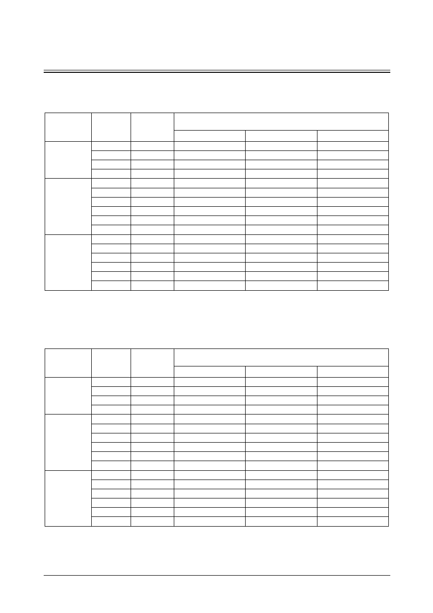
SEC ASIC
4-40
STDH90/MDL90
PHOTyz
Tri-State Output Buffers
PHOT24SM Switching Characteristics
[Delays for typical process, 25 C, 5.0V, when t , t = 0.80ns]
o
R F
(CL : Capacitive Load[pf])
Path
Parameter
Delay [ns]
CL = 50.0pF
Delay Equations [ns]
Group1*
Group2*
Group3*
A to PAD
tR
1.957
0.299 + 0.033*CL
0.274 + 0.033*CL
0.265 + 0.034*CL
tF
2.025
0.613 + 0.028*CL
0.601 + 0.028*CL
0.607 + 0.028*CL
tPLH
2.614
1.808 + 0.016*CL
1.825 + 0.016*CL
1.822 + 0.016*CL
tPHL
2.875
1.991 + 0.018*CL
2.049 + 0.017*CL
2.086 + 0.016*CL
TN to PAD
tR
1.956
0.296 + 0.033*CL
0.266 + 0.034*CL
0.272 + 0.034*CL
tF
2.023
0.605 + 0.028*CL
0.617 + 0.028*CL
0.600 + 0.028*CL
tPLH
2.614
1.808 + 0.016*CL
1.825 + 0.016*CL
1.822 + 0.016*CL
tPHL
2.996
2.114 + 0.018*CL
2.147 + 0.017*CL
2.209 + 0.016*CL
tPLZ
1.629
1.629 + 0.000*CL
1.629 + 0.000*CL
1.629 + 0.000*CL
tPHZ
1.875
1.875 + 0.000*CL
1.872 + 0.000*CL
1.872 + 0.000*CL
EN to PAD
tR
1.957
0.297 + 0.033*CL
0.282 + 0.033*CL
0.265 + 0.034*CL
tF
2.023
0.605 + 0.028*CL
0.617 + 0.028*CL
0.606 + 0.028*CL
tPLH
2.901
2.095 + 0.016*CL
2.126 + 0.016*CL
2.095 + 0.016*CL
tPHL
3.291
2.409 + 0.018*CL
2.472 + 0.017*CL
2.495 + 0.017*CL
tPLZ
1.326
1.326 + 0.000*CL
1.326 + 0.000*CL
1.326 + 0.000*CL
tPHZ
1.562
1.562 + 0.000*CL
1.569 + 0.000*CL
1.561 + 0.000*CL
*Group1 : CL < 75, *Group2 : 75 CL 85, *Group3 : 85 < CL
< <
= =
PHOT24SH Switching Characteristics
[Delays for typical process, 25 C, 5.0V, when t , t = 0.80ns]
o
R F
(CL : Capacitive Load[pf])
Path
Parameter
Delay [ns]
CL = 50.0pF
Delay Equations [ns]
Group1*
Group2*
Group3*
A to PAD
tR
1.958
0.298 + 0.033*CL
0.268 + 0.034*CL
0.268 + 0.034*CL
tF
2.018
0.590 + 0.029*CL
0.595 + 0.028*CL
0.603 + 0.028*CL
tPLH
3.346
2.534 + 0.016*CL
2.552 + 0.016*CL
2.552 + 0.016*CL
tPHL
3.207
2.313 + 0.018*CL
2.379 + 0.017*CL
2.402 + 0.017*CL
TN to PAD
tR
1.954
0.292 + 0.033*CL
0.265 + 0.034*CL
0.265 + 0.034*CL
tF
2.016
0.586 + 0.029*CL
0.593 + 0.029*CL
0.602 + 0.028*CL
tPLH
3.291
2.481 + 0.016*CL
2.488 + 0.016*CL
2.503 + 0.016*CL
tPHL
3.297
2.403 + 0.018*CL
2.439 + 0.017*CL
2.501 + 0.017*CL
tPLZ
1.798
1.798 + 0.000*CL
1.798 + 0.000*CL
1.798 + 0.000*CL
tPHZ
1.772
1.772 + 0.000*CL
1.772 + 0.000*CL
1.772 + 0.000*CL
EN to PAD
tR
1.955
0.293 + 0.033*CL
0.274 + 0.033*CL
0.259 + 0.034*CL
tF
2.017
0.589 + 0.029*CL
0.593 + 0.029*CL
0.602 + 0.028*CL
tPLH
3.579
2.771 + 0.016*CL
2.798 + 0.016*CL
2.775 + 0.016*CL
tPHL
3.593
2.701 + 0.018*CL
2.757 + 0.017*CL
2.793 + 0.017*CL
tPLZ
1.495
1.495 + 0.000*CL
1.495 + 0.000*CL
1.495 + 0.000*CL
tPHZ
1.467
1.467 + 0.000*CL
1.467 + 0.000*CL
1.467 + 0.000*CL
*Group1 : CL < 75, *Group2 : 75 CL 85, *Group3 : 85 < CL
< <
= =

STDH90/MDL90
4-41
SEC ASIC
BI-DIRECTIONAL BUFFERS
Cell List
Cell Name
Function Description
PHBaDyz
5V Open-Drain Bi-Directional Buffers
PHBaU50Dyz
5V Open-Drain Bi-Directional Buffers with Pull-Up
PHBaTyz
5V Tri-State Bi-Directional Buffers
PHBaD50Tyz
5V Tri-State Bi-Directional Buffers with Pull-Down
PHBaU50Tyz
5V Tri-State Bi-Directional Buffers with Pull-Up
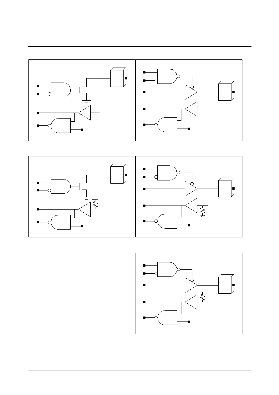
SEC ASIC
4-42
STDH90/MDL90
PHBaDyz/PHBaU50Dyz
Open Drain Bi-Directional Buffers
PHBaDyz
PHBaU50Dyz
PAD
TN
EN
Y
PO
PI
PAD
TN
EN
Y
PO
PI
PHBaTyz/PHBaD50Tyz/PHBaU50Tyz
Tri-State Bi-Directional Buffers
PHBaTyz
PHBaD50Tyz
PHBaU50Tyz
PAD
A
TN
EN
Y
PO
PI
PAD
A
TN
EN
Y
PO
PI
PAD
A
TN
EN
Y
PO
PI

STDH90/MDL90
4-43
SEC ASIC
CLOCK DRIVERS
Cell List
Cell Name
Function Description
CK(2/3/4)X
CMOS Level Clock Driver
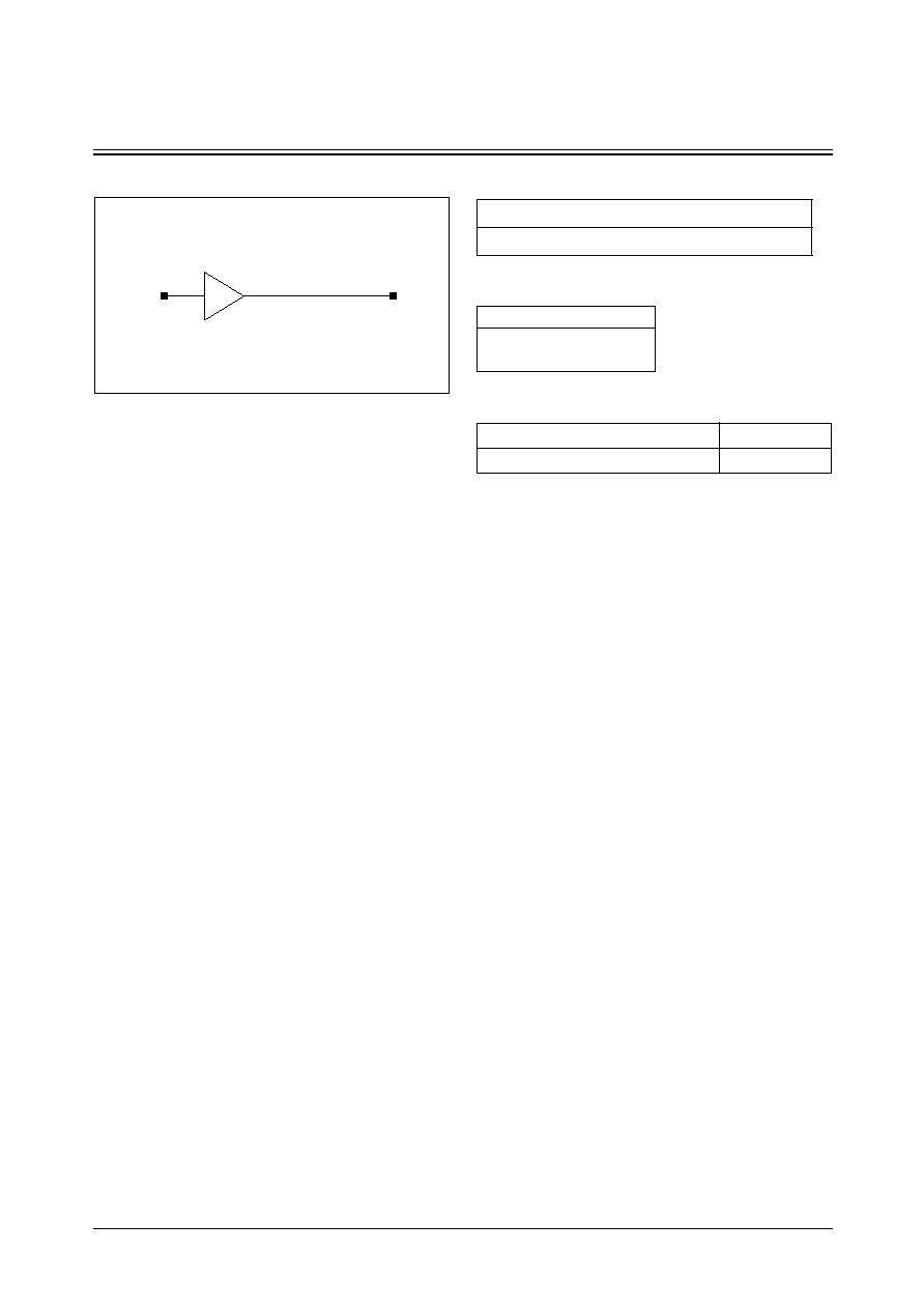
SEC ASIC
4-44
STDH90/MDL90
CKyX
CMOS Level Clock Drivers
Logic Symbol
Y
A
Cell Availability
Truth Table
Standard Load (SL)
3.3V Interface
CK(2/3/4)X
A
Y
1
1
0
0
Cell Name
PI
CK(2/3/4)X
4.4

STDH90/MDL90
4-45
SEC ASIC
CKyX
CMOS Level Clock Drivers
CK2X Switching Characteristics
[Delays for typical process, 25 C, 3.3V, when t , t = 0.80ns]
o
R F
(SL : Standard Load)
Path
Parameter
Delay [ns]
SL = 2
Delay Equations [ns]
Group1*
Group2*
Group3*
A to Y
tR
0.354
0.352 + 0.001*SL
0.359 + 0.001*SL
0.349 + 0.001*SL
tF
0.458
0.457 + 0.001*SL
0.505 + 0.001*SL
0.537 + 0.001*SL
tPLH
1.283
1.281 + 0.001*SL
1.335 + 0.000*SL
1.367 + 0.000*SL
tPHL
1.682
1.680 + 0.001*SL
1.779 + 0.001*SL
1.855 + 0.001*SL
*Group1 : SL < 200, *Group2 : 200 SL 400, *Group3 : 400 < SL
< <
= =
CK3X Switching Characteristics
[Delays for typical process, 25 C, 3.3V, when t , t = 0.80ns]
o
R F
(SL : Standard Load)
Path
Parameter
Delay [ns]
SL = 2
Delay Equations [ns]
Group1*
Group2*
Group3*
A to Y
tR
0.361
0.360 + 0.001*SL
0.380 + 0.001*SL
0.406 + 0.001*SL
tF
0.452
0.451 + 0.001*SL
0.508 + 0.001*SL
0.562 + 0.001*SL
tPLH
1.358
1.357 + 0.000*SL
1.423 + 0.000*SL
1.471 + 0.000*SL
tPHL
1.800
1.799 + 0.001*SL
1.898 + 0.000*SL
1.982 + 0.000*SL
*Group1 : SL < 200, *Group2 : 200 SL 400, *Group3 : 400 < SL
< <
= =
CK4X Switching Characteristics
[Delays for typical process, 25 C, 3.3V, when t , t = 0.80ns]
o
R F
(SL : Standard Load)
Path
Parameter
Delay [ns]
SL = 2
Delay Equations [ns]
Group1*
Group2*
Group3*
A to Y
tR
0.369
0.368 + 0.001*SL
0.405 + 0.000*SL
0.421 + 0.000*SL
tF
0.477
0.476 + 0.001*SL
0.535 + 0.000*SL
0.585 + 0.000*SL
tPLH
1.432
1.431 + 0.000*SL
1.504 + 0.000*SL
1.562 + 0.000*SL
tPHL
1.890
1.888 + 0.001*SL
1.989 + 0.000*SL
2.077 + 0.000*SL
*Group1 : SL < 200, *Group2 : 200 SL 400, *Group3 : 400 < SL
< <
= =

SEC ASIC
4-46
STDH90/MDL90
OSCILLATORS
Cell List
Cell Name
Function Description
PHSOSCLF
Oscillator Cell (1KHz ~ 10MHz)
PHSOSCMF
Oscillator Cell (10MHz ~ 40MHz)
PHSOSCHF
Oscillator Cell (50MHz and 60MHz)

STDH90/MDL90
4-47
SEC ASIC
PHSOSCLF
Oscillator Cell (1KHz ~ 10MHz)
Logic Symbol
Truth Table
PADA
PADY
Y
0
1
0
1
0
1
PADA
PADY
Y
SEC ASIC
4-48
STDH90/MDL90
PHSOSCLF
Oscillators
PHSOSCLF Switching Characteristics
[Delays for typical process, 25 C, 5.0V, when t , t = 0.80ns]
o
R F
(CL : Capacitive Load[pf])
Path
Parameter
Delay [ns]
CL = 50.0pF
Delay Equations [ns]
Group1*
Group2*
Group3*
PADA to PADY
tR
10.113
0.791 + 0.186*CL
0.623 + 0.203*CL
0.484 + 0.206*CL
tF
8.497
0.781 + 0.154*CL
0.573 + 0.175*CL
0.414 + 0.178*CL
tPLH
5.581
0.736 + 0.097*CL
0.763 + 0.094*CL
0.738 + 0.095*CL
tPHL
5.375
0.630 + 0.095*CL
0.658 + 0.092*CL
0.632 + 0.093*CL
*Group1 : CL < 75, *Group2 : 75 CL 85, *Group3 : 85 < CL
< <
= =
[Delays for typical process, 25 C, 3.3V, when t , t = 0.80ns]
o
R F
(SL : Standard Load)
Path
Parameter
Delay [ns]
SL = 2
Delay Equations [ns]
Group1*
Group2*
Group3*
PADY to Y
tR
0.114
0.100 + 0.007*SL
0.119 + 0.003*SL
0.117 + 0.003*SL
tF
0.087
0.071 + 0.008*SL
0.100 + 0.002*SL
0.097 + 0.002*SL
tPLH
0.823
0.816 + 0.004*SL
0.825 + 0.002*SL
0.830 + 0.002*SL
tPHL
0.592
0.587 + 0.003*SL
0.594 + 0.001*SL
0.603 + 0.001*SL
*Group1 : SL < 3, *Group2 : 3 SL 43, *Group3 : 43 < SL
< <
= =
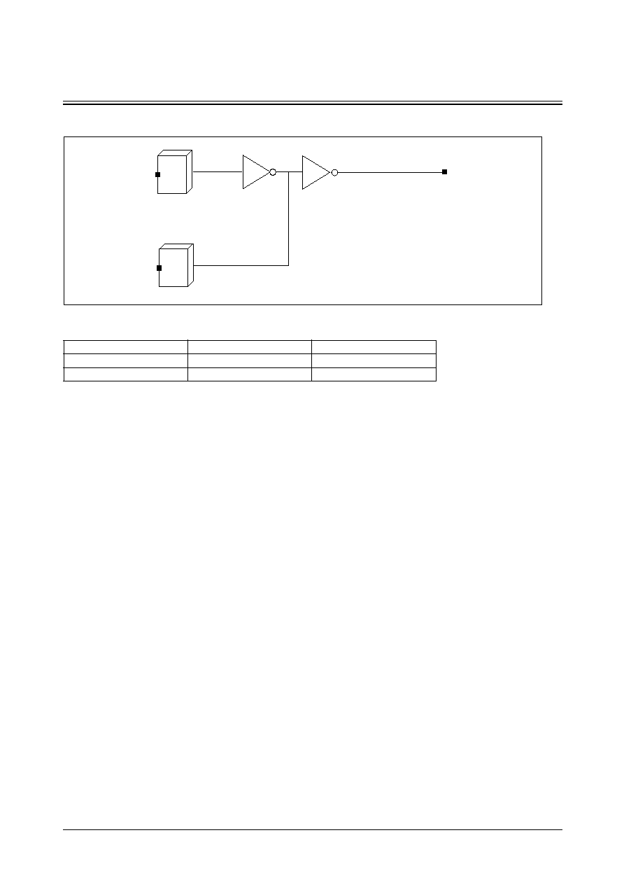
STDH90/MDL90
4-49
SEC ASIC
PHSOSCMF
Oscillator Cell (10MHz ~ 25MHz)
Logic Symbol
Truth Table
PADA
PADY
Y
0
1
0
1
0
1
PADA
PADY
Y

SEC ASIC
4-50
STDH90/MDL90
PHSOSCMF
Oscillators
PHSOSCMF Switching Characteristics
[Delays for typical process, 25 C, 5.0V, when t , t = 0.80ns]
o
R F
(CL : Capacitive Load[pf])
Path
Parameter
Delay [ns]
CL = 50.0pF
Delay Equations [ns]
Group1*
Group2*
Group3*
PADA to PADY
tR
3.553
0.631 + 0.058*CL
0.571 + 0.064*CL
0.436 + 0.067*CL
tF
3.082
0.632 + 0.049*CL
0.583 + 0.054*CL
0.403 + 0.057*CL
tPLH
2.846
0.801 + 0.041*CL
0.886 + 0.032*CL
0.934 + 0.031*CL
tPHL
2.751
0.729 + 0.040*CL
0.820 + 0.031*CL
0.854 + 0.031*CL
*Group1 : CL < 75, *Group2 : 75 CL 85, *Group3 : 85 < CL
< <
= =
[Delays for typical process, 25 C, 3.3V, when t , t = 0.80ns]
o
R F
(SL : Standard Load)
Path
Parameter
Delay [ns]
SL = 2
Delay Equations [ns]
Group1*
Group2*
Group3*
PADY to Y
tR
0.129
0.124 + 0.002*SL
0.125 + 0.002*SL
0.118 + 0.002*SL
tF
0.108
0.106 + 0.001*SL
0.103 + 0.001*SL
0.118 + 0.001*SL
tPLH
0.844
0.841 + 0.002*SL
0.842 + 0.001*SL
0.846 + 0.001*SL
tPHL
0.614
0.611 + 0.002*SL
0.615 + 0.001*SL
0.616 + 0.001*SL
*Group1 : SL < 3, *Group2 : 3 SL 43, *Group3 : 43 < SL
< <
= =
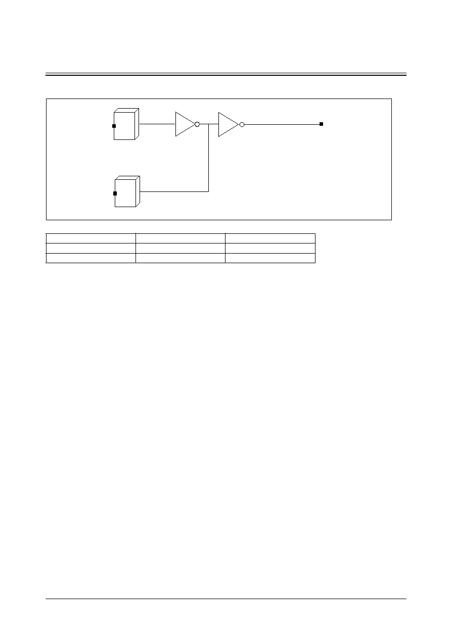
STDH90/MDL90
4-51
SEC ASIC
PHSOSCHF
Oscillator Cell (50MHz and 60MHz)
Logic Symbol
Truth Table
PADA
PADY
Y
0
1
0
1
0
1
PADA
PADY
Y

SEC ASIC
4-52
STDH90/MDL90
PHSOSCHF
Oscillators
PHSOSCHF Switching Characteristics
[Delays for typical process, 25 C, 5.0V, when t , t = 0.80ns]
o
R F
(CL : Capacitive Load[pf])
Path
Parameter
Delay [ns]
CL = 50.0pF
Delay Equations [ns]
Group1*
Group2*
Group3*
PADA to PADY
tR
2.227
0.716 + 0.030*CL
0.702 + 0.032*CL
0.645 + 0.033*CL
tF
2.158
0.669 + 0.030*CL
0.702 + 0.026*CL
0.658 + 0.027*CL
tPLH
2.461
1.066 + 0.028*CL
1.154 + 0.019*CL
1.258 + 0.017*CL
tPHL
2.340
1.024 + 0.026*CL
1.101 + 0.019*CL
1.212 + 0.016*CL
*Group1 : CL < 75, *Group2 : 75 CL 85, *Group3 : 85 < CL
< <
= =
[Delays for typical process, 25 C, 3.3V, when t , t = 0.80ns]
o
R F
(SL : Standard Load)
Path
Parameter
Delay [ns]
SL = 2
Delay Equations [ns]
Group1*
Group2*
Group3*
PADY to Y
tR
0.134
0.132 + 0.001*SL
0.129 + 0.002*SL
0.145 + 0.001*SL
tF
0.113
0.111 + 0.001*SL
0.109 + 0.001*SL
0.115 + 0.001*SL
tPLH
0.878
0.871 + 0.003*SL
0.881 + 0.001*SL
0.901 + 0.001*SL
tPHL
0.629
0.626 + 0.001*SL
0.628 + 0.001*SL
0.641 + 0.001*SL
*Group1 : SL < 3, *Group2 : 3 SL 43, *Group3 : 43 < SL
< <
= =

STDH90/MDL90
4-53
SEC ASIC
ATA2 Interface with no fail safe
Cell List
Cell Name
Function Description
PHOD24ATA2
ATA2 Open Drain Output Buffer
PHOT24ATA2
ATA2 Tri-State Output Buffer
PHOT24CATA2
ATA2 Controlled Tri-State Output Buffer
PHOTC24ATA2
PHOTC8ATA2
PHOT8CATA2
PHBLU50D24ATA2
ATA2 Open Drain Bi-Directional Buffer
PHBLU50T24ATA2
ATA2 Tri-State Bi-Directional Buffer
PHBLU50TC8ATA2
ATA2 Controlled Tri-State Bi-Directional Buffer
PHBLU50T8CATA2
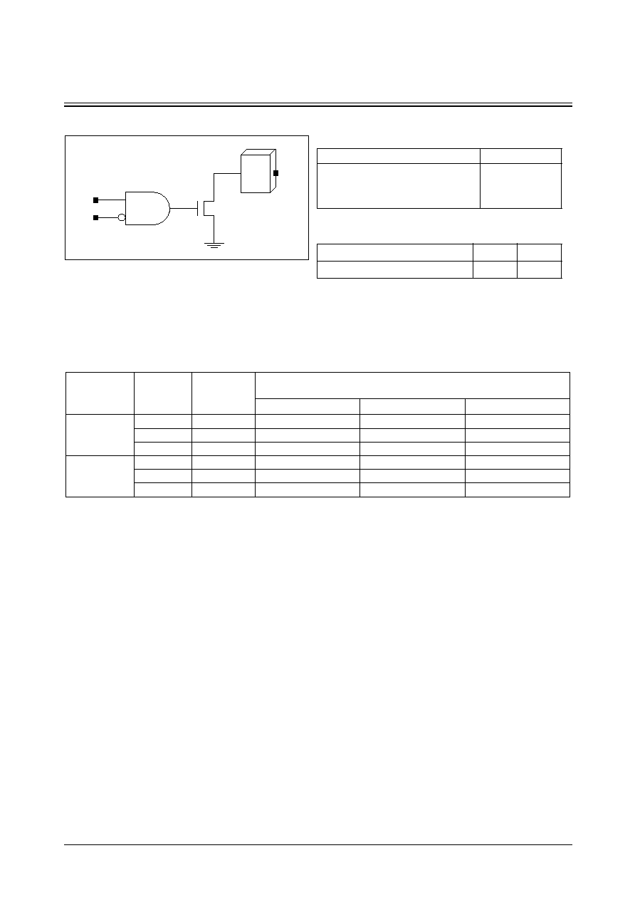
SEC ASIC
4-54
STDH90/MDL90
PHOD24ATA2
ATA2 Open Drain Output Buffer
Logic Symbol
PAD
TN
EN
PHOD24ATA2 Switching Characteristics
[Delays for typical process, 25 C, 5.0V, when t , t = 0.80ns]
o
R F
(CL : Capacitive Load[pf])
Path
Parameter
Delay [ns]
CL = 50.0pF
Delay Equations [ns]
Group1*
Group2*
Group3*
TN to PAD
tF
2.606
0.470 + 0.043*CL
0.449 + 0.043*CL
0.421 + 0.043*CL
tPHL
3.211
2.001 + 0.024*CL
2.039 + 0.024*CL
2.053 + 0.024*CL
tPLZ
1.664
1.664 + 0.000*CL
1.664 + 0.000*CL
1.664 + 0.000*CL
EN to PAD
tF
2.606
0.470 + 0.043*CL
0.441 + 0.043*CL
0.427 + 0.043*CL
tPHL
3.504
2.294 + 0.024*CL
2.331 + 0.024*CL
2.346 + 0.024*CL
tPLZ
1.358
1.358 + 0.000*CL
1.358 + 0.000*CL
1.358 + 0.000*CL
*Group1 : CL < 75, *Group2 : 75 CL 85, *Group3 : 85 < CL
< <
= =
Truth Table
Standard Load (SL)
TN
EN
PAD
1
0
0
0
x
Hi-Z
x
1
Hi-Z
Cell Name
TN
EN
PHOD24ATA2
2.1
2.4
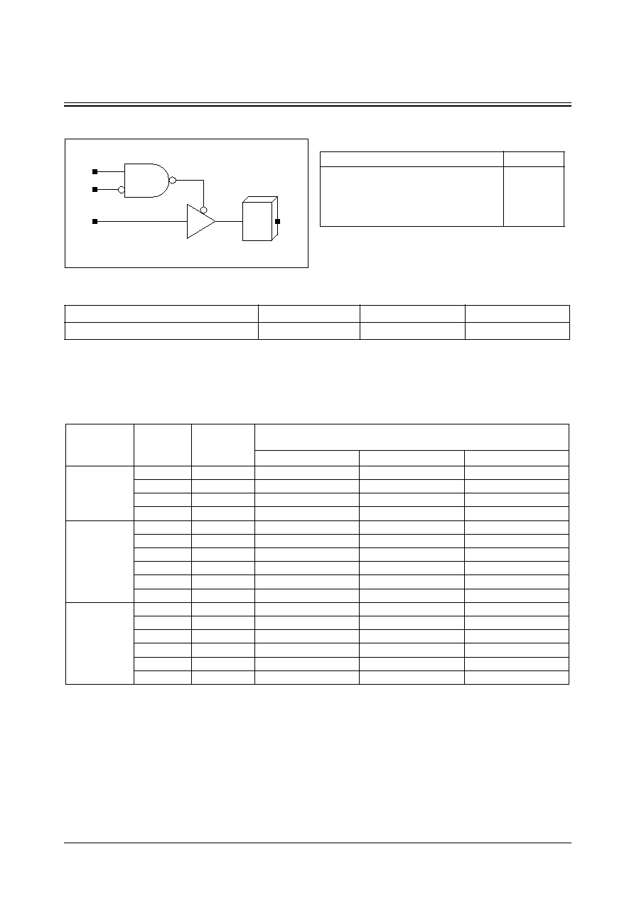
STDH90/MDL90
4-55
SEC ASIC
PHOT24ATA2
ATA2 Tri-State Output Buffer
Logic Symbol
Standard Load (SL)
Cell Name
TN
EN
A
PHOT24ATA2
2.1
2.4
5.7
PAD
A
TN
EN
PHOT24ATA2 Switching Characteristics
[Delays for typical process, 25 C, 5.0V, when t , t = 0.80ns]
o
R F
(CL : Capacitive Load[pf])
Path
Parameter
Delay [ns]
CL = 50.0pF
Delay Equations [ns]
Group1*
Group2*
Group3*
A to PAD
tR
2.783
0.245 + 0.051*CL
0.227 + 0.051*CL
0.221 + 0.051*CL
tF
2.637
0.497 + 0.043*CL
0.475 + 0.043*CL
0.460 + 0.043*CL
tPLH
3.627
2.433 + 0.024*CL
2.439 + 0.024*CL
2.445 + 0.024*CL
tPHL
3.409
2.195 + 0.024*CL
2.231 + 0.024*CL
2.248 + 0.024*CL
TN to PAD
tR
2.781
0.243 + 0.051*CL
0.225 + 0.051*CL
0.214 + 0.051*CL
tF
2.636
0.494 + 0.043*CL
0.475 + 0.043*CL
0.460 + 0.043*CL
tPLH
3.578
2.384 + 0.024*CL
2.390 + 0.024*CL
2.390 + 0.024*CL
tPHL
3.501
2.285 + 0.024*CL
2.301 + 0.024*CL
2.344 + 0.024*CL
tPLZ
1.737
1.737 + 0.000*CL
1.737 + 0.000*CL
1.737 + 0.000*CL
tPHZ
1.674
1.674 + 0.000*CL
1.674 + 0.000*CL
1.674 + 0.000*CL
EN to PAD
tR
2.782
0.246 + 0.051*CL
0.225 + 0.051*CL
0.214 + 0.051*CL
tF
2.636
0.492 + 0.043*CL
0.475 + 0.043*CL
0.467 + 0.043*CL
tPLH
3.863
2.669 + 0.024*CL
2.690 + 0.024*CL
2.667 + 0.024*CL
tPHL
3.797
2.583 + 0.024*CL
2.619 + 0.024*CL
2.636 + 0.024*CL
tPLZ
1.438
1.438 + 0.000*CL
1.438 + 0.000*CL
1.438 + 0.000*CL
tPHZ
1.367
1.367 + 0.000*CL
1.367 + 0.000*CL
1.367 + 0.000*CL
*Group1 : CL < 75, *Group2 : 75 CL 85, *Group3 : 85 < CL
< <
= =
Truth Table
TN
EN
A
PAD
1
0
0
0
1
0
1
1
x
1
x
Hi-Z
0
x
x
Hi-Z
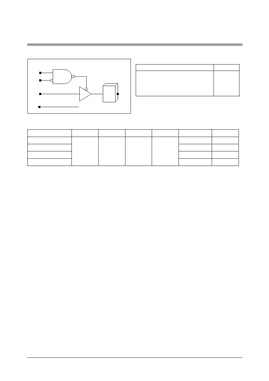
SEC ASIC
4-56
STDH90/MDL90
PHOT24CATA2/PHOTC24ATA2/PHOTC8ATA2/PHOT8CATA2
ATA2 Controlled Tri-State Output Buffers
Logic Symbol
Standard Load (SL)
Cell Name
TN
EN
A
OPOW
CONTROL
IOL
PHOT24CATA2
2.1
2.4
5.7
5.7
OPOW=H
24mA
PHOTC24ATA2
OPOW=L
12mA
PHOTC8ATA2
OPOW=H
12mA
PHOT8CATA2
OPOW=L
8mA
PAD
A
TN
EN
OPOW
Truth Table
TN
EN
A
PAD
1
0
0
0
1
0
1
1
x
1
x
Hi-Z
0
x
x
Hi-Z

STDH90/MDL90
4-57
SEC ASIC
PHOT24CATA2/PHOTC24ATA2/PHOTC8ATA2/PHOT8CATA2
ATA2 Controlled Tri-State Output Buffers
PHOT24CATA2 Switching Characteristics
[Delays for typical process, 25 C, 5.0V, when t , t = 0.80ns]
o
R F
(CL : Capacitive Load[pf])
Path
Parameter
Delay [ns]
CL = 50.0pF
Delay Equations [ns]
Group1*
Group2*
Group3*
A to PAD
tR
2.729
0.167 + 0.051*CL
0.155 + 0.051*CL
0.155 + 0.051*CL
tF
2.457
0.281 + 0.044*CL
0.260 + 0.044*CL
0.249 + 0.044*CL
tPLH
2.778
1.592 + 0.024*CL
1.586 + 0.024*CL
1.592 + 0.024*CL
tPHL
2.790
1.622 + 0.023*CL
1.626 + 0.023*CL
1.635 + 0.023*CL
TN to PAD
tR
2.741
0.195 + 0.051*CL
0.167 + 0.051*CL
0.169 + 0.051*CL
tF
2.466
0.296 + 0.043*CL
0.273 + 0.044*CL
0.259 + 0.044*CL
tPLH
2.869
1.683 + 0.024*CL
1.692 + 0.024*CL
1.669 + 0.024*CL
tPHL
2.987
1.819 + 0.023*CL
1.793 + 0.024*CL
1.859 + 0.023*CL
tPLZ
1.547
1.547 + 0.000*CL
1.592 + 0.000*CL
1.541 + 0.000*CL
tPHZ
1.503
1.503 + 0.000*CL
1.503 + 0.000*CL
1.503 + 0.000*CL
EN to PAD
tR
2.741
0.193 + 0.051*CL
0.175 + 0.051*CL
0.164 + 0.051*CL
tF
2.466
0.296 + 0.043*CL
0.273 + 0.044*CL
0.259 + 0.044*CL
tPLH
3.156
1.968 + 0.024*CL
1.965 + 0.024*CL
1.965 + 0.024*CL
tPHL
3.275
2.107 + 0.023*CL
2.111 + 0.023*CL
2.120 + 0.023*CL
tPLZ
1.239
1.239 + 0.000*CL
1.239 + 0.000*CL
1.250 + 0.000*CL
tPHZ
1.200
1.200 + 0.000*CL
1.200 + 0.000*CL
1.200 + 0.000*CL
*Group1 : CL < 75, *Group2 : 75 CL 85, *Group3 : 85 < CL
< <
= =
PHOTC24ATA2 Switching Characteristics
[Delays for typical process, 25 C, 5.0V, when t , t = 0.80ns]
o
R F
(CL : Capacitive Load[pf])
Path
Parameter
Delay [ns]
CL = 50.0pF
Delay Equations [ns]
Group1*
Group2*
Group3*
A to PAD
tR
5.400
0.252 + 0.103*CL
0.249 + 0.103*CL
0.249 + 0.103*CL
tF
4.734
0.314 + 0.088*CL
0.284 + 0.089*CL
0.284 + 0.089*CL
tPLH
4.007
1.635 + 0.047*CL
1.631 + 0.047*CL
1.628 + 0.048*CL
tPHL
3.970
1.650 + 0.046*CL
1.658 + 0.046*CL
1.649 + 0.046*CL
TN to PAD
tR
5.400
0.252 + 0.103*CL
0.249 + 0.103*CL
0.249 + 0.103*CL
tF
4.734
0.314 + 0.088*CL
0.284 + 0.089*CL
0.284 + 0.089*CL
tPLH
3.952
1.580 + 0.047*CL
1.583 + 0.047*CL
1.577 + 0.047*CL
tPHL
4.057
1.737 + 0.046*CL
1.737 + 0.046*CL
1.743 + 0.046*CL
tPLZ
1.537
1.537 + 0.000*CL
1.514 + 0.000*CL
1.540 + 0.000*CL
tPHZ
1.521
1.521 + 0.000*CL
1.521 + 0.000*CL
1.521 + 0.000*CL
EN to PAD
tR
5.400
0.252 + 0.103*CL
0.249 + 0.103*CL
0.249 + 0.103*CL
tF
4.734
0.314 + 0.088*CL
0.291 + 0.089*CL
0.277 + 0.089*CL
tPLH
4.238
1.864 + 0.047*CL
1.870 + 0.047*CL
1.864 + 0.047*CL
tPHL
4.354
2.034 + 0.046*CL
2.034 + 0.046*CL
2.040 + 0.046*CL
tPLZ
1.228
1.228 + 0.000*CL
1.228 + 0.000*CL
1.228 + 0.000*CL
tPHZ
1.217
1.217 + 0.000*CL
1.217 + 0.000*CL
1.217 + 0.000*CL
*Group1 : CL < 75, *Group2 : 75 CL 85, *Group3 : 85 < CL
< <
= =

SEC ASIC
4-58
STDH90/MDL90
PHOT24CATA2/PHOTC24ATA2/PHOTC8ATA2/PHOT8CATA2
ATA2 Controlled Tri-State Output Buffers
PHOTC8ATA2 Switching Characteristics
[Delays for typical process, 25 C, 5.0V, when t , t = 0.80ns]
o
R F
(CL : Capacitive Load[pf])
Path
Parameter
Delay [ns]
CL = 50.0pF
Delay Equations [ns]
Group1*
Group2*
Group3*
A to PAD
tR
5.395
0.247 + 0.103*CL
0.244 + 0.103*CL
0.244 + 0.103*CL
tF
4.716
0.290 + 0.089*CL
0.269 + 0.089*CL
0.263 + 0.089*CL
tPLH
3.911
1.539 + 0.047*CL
1.535 + 0.047*CL
1.537 + 0.047*CL
tPHL
3.876
1.556 + 0.046*CL
1.549 + 0.046*CL
1.563 + 0.046*CL
TN to PAD
tR
5.395
0.247 + 0.103*CL
0.251 + 0.103*CL
0.237 + 0.103*CL
tF
4.713
0.285 + 0.089*CL
0.259 + 0.089*CL
0.262 + 0.089*CL
tPLH
3.923
1.549 + 0.047*CL
1.533 + 0.048*CL
1.552 + 0.047*CL
tPHL
4.010
1.692 + 0.046*CL
1.666 + 0.047*CL
1.709 + 0.046*CL
tPLZ
1.551
1.551 + 0.000*CL
1.589 + 0.000*CL
1.546 + 0.000*CL
tPHZ
1.506
1.506 + 0.000*CL
1.506 + 0.000*CL
1.506 + 0.000*CL
EN to PAD
tR
5.395
0.247 + 0.103*CL
0.244 + 0.103*CL
0.244 + 0.103*CL
tF
4.713
0.285 + 0.089*CL
0.259 + 0.089*CL
0.262 + 0.089*CL
tPLH
4.214
1.840 + 0.047*CL
1.846 + 0.047*CL
1.846 + 0.047*CL
tPHL
4.300
1.980 + 0.046*CL
1.980 + 0.046*CL
1.986 + 0.046*CL
tPLZ
1.240
1.240 + 0.000*CL
1.240 + 0.000*CL
1.240 + 0.000*CL
tPHZ
1.205
1.205 + 0.000*CL
1.205 + 0.000*CL
1.205 + 0.000*CL
*Group1 : CL < 75, *Group2 : 75 CL 85, *Group3 : 85 < CL
< <
= =
PHOT8CATA2 Switching Characteristics
[Delays for typical process, 25 C, 5.0V, when t , t = 0.80ns]
o
R F
(CL : Capacitive Load[pf])
Path
Parameter
Delay [ns]
CL = 50.0pF
Delay Equations [ns]
Group1*
Group2*
Group3*
A to PAD
tR
7.182
0.314 + 0.137*CL
0.319 + 0.137*CL
0.310 + 0.137*CL
tF
6.257
0.339 + 0.118*CL
0.321 + 0.119*CL
0.310 + 0.119*CL
tPLH
4.797
1.635 + 0.063*CL
1.631 + 0.063*CL
1.633 + 0.063*CL
tPHL
4.712
1.620 + 0.062*CL
1.615 + 0.062*CL
1.624 + 0.062*CL
TN to PAD
tR
7.182
0.314 + 0.137*CL
0.319 + 0.137*CL
0.310 + 0.137*CL
tF
6.257
0.339 + 0.118*CL
0.313 + 0.119*CL
0.316 + 0.119*CL
tPLH
4.745
1.581 + 0.063*CL
1.587 + 0.063*CL
1.581 + 0.063*CL
tPHL
4.805
1.711 + 0.062*CL
1.717 + 0.062*CL
1.717 + 0.062*CL
tPLZ
1.540
1.540 + 0.000*CL
1.510 + 0.000*CL
1.544 + 0.000*CL
tPHZ
1.507
1.507 + 0.000*CL
1.507 + 0.000*CL
1.507 + 0.000*CL
EN to PAD
tR
7.182
0.314 + 0.137*CL
0.319 + 0.137*CL
0.310 + 0.137*CL
tF
6.257
0.339 + 0.118*CL
0.321 + 0.119*CL
0.310 + 0.119*CL
tPLH
5.033
1.869 + 0.063*CL
1.868 + 0.063*CL
1.870 + 0.063*CL
tPHL
5.097
2.005 + 0.062*CL
2.008 + 0.062*CL
2.002 + 0.062*CL
tPLZ
1.230
1.230 + 0.000*CL
1.230 + 0.000*CL
1.230 + 0.000*CL
tPHZ
1.204
1.204 + 0.000*CL
1.204 + 0.000*CL
1.204 + 0.000*CL
*Group1 : CL < 75, *Group2 : 75 CL 85, *Group3 : 85 < CL
< <
= =
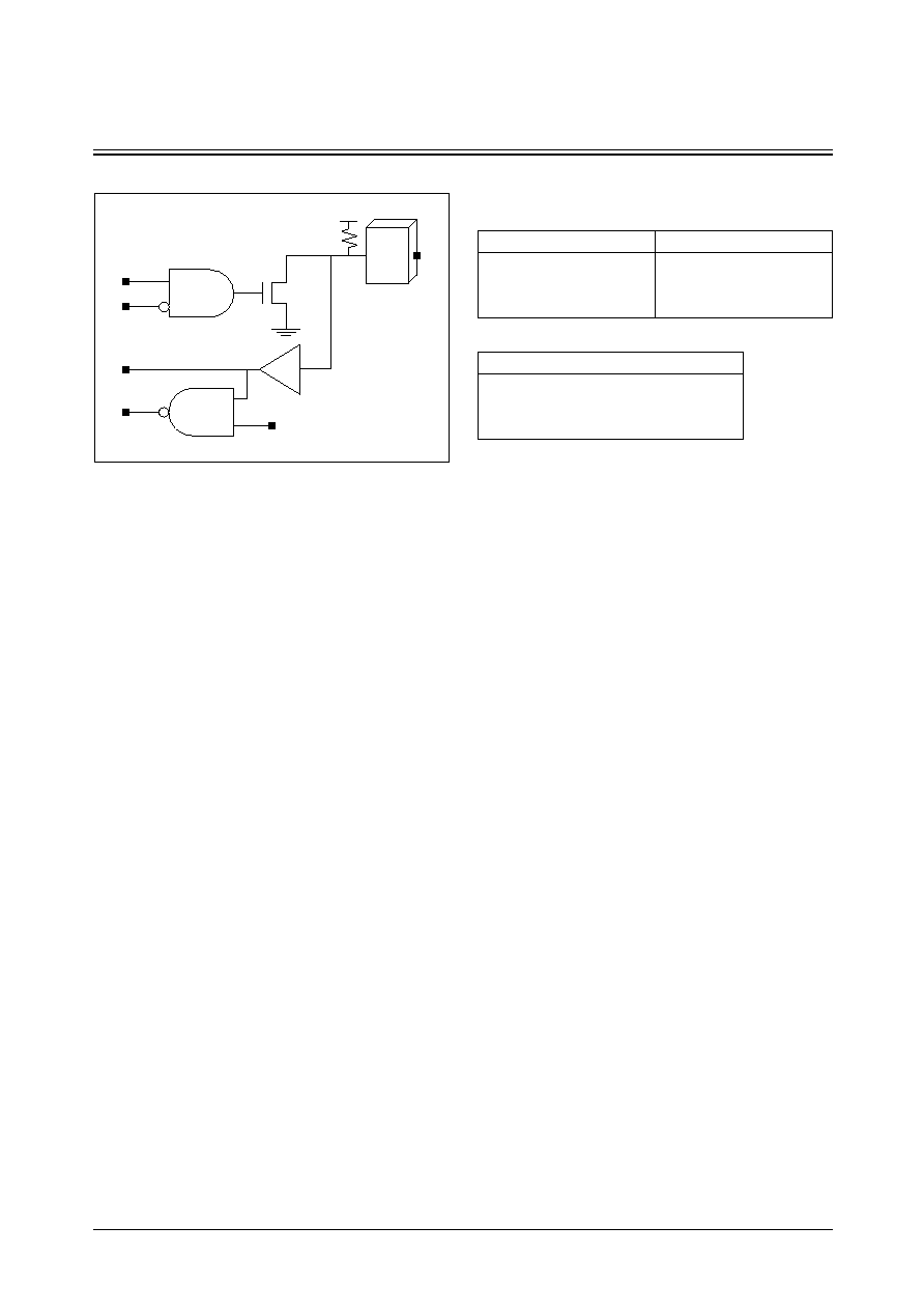
STDH90/MDL90
4-59
SEC ASIC
PHBLU50D24ATA2
ATA2 Open Drain Bidirectional Buffer
Logic Symbol
PAD
TN
EN
Y
PO
PI
Truth Table
Input Truth Table
Output Truth Table
PAD
PI
Y
PO
1
1
1
0
0
x
0
1
1
0
1
1
EN
TN
PAD
0
1
0
1
x
Hi-Z
x
0
Hi-Z

SEC ASIC
4-60
STDH90/MDL90
PHBTU50T24ATA2
ATA2 Tri-State Bidirectional Buffer
Logic Symbol
PAD
A
TN
EN
Y
PO
PI
Truth Table
Input Truth Table
Output Truth Table
PAD
PI
Y
PO
1
1
1
0
0
x
0
1
1
0
1
1
A
EN
TN
PAD
0
0
1
0
1
0
1
1
x
1
x
Hi-Z
x
x
0
Hi-Z
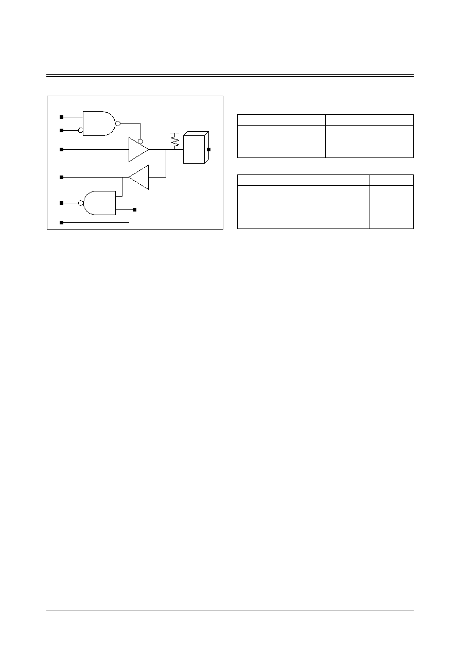
STDH90/MDL90
4-61
SEC ASIC
PHBLU50TC8ATA2/PHBLU50T8CATA2
ATA2 Controlled Tri-State Bidirectional Buffers
Logic Symbol
PAD
A
TN
EN
Y
PO
PI
OPOW
Truth Table
Input Truth Table
Output Truth Table
PAD
PI
Y
PO
1
1
1
0
0
x
0
1
1
0
1
1
A
EN
TN
PAD
0
0
1
0
1
0
1
1
x
1
x
Hi-Z
x
x
0
Hi-Z
SEC ASIC
4-62
STDH90/MDL90
ATA3 Interface with fail safe
Cell List
Cell Name
Function Description
PHITATA
ATA3 Input Buffers
PHITU50ATA
PHSOT12S1FATA
ATA2 Tri-State Output Buffer
PHSOT4S1FATA
PHSBTT4S1FATA
ATA3 Tri-State Bi-Directional Buffers
PHSBTT12S1FATA
PHSBTU50T4S1FATA
PHSBTU50T12S1FATA
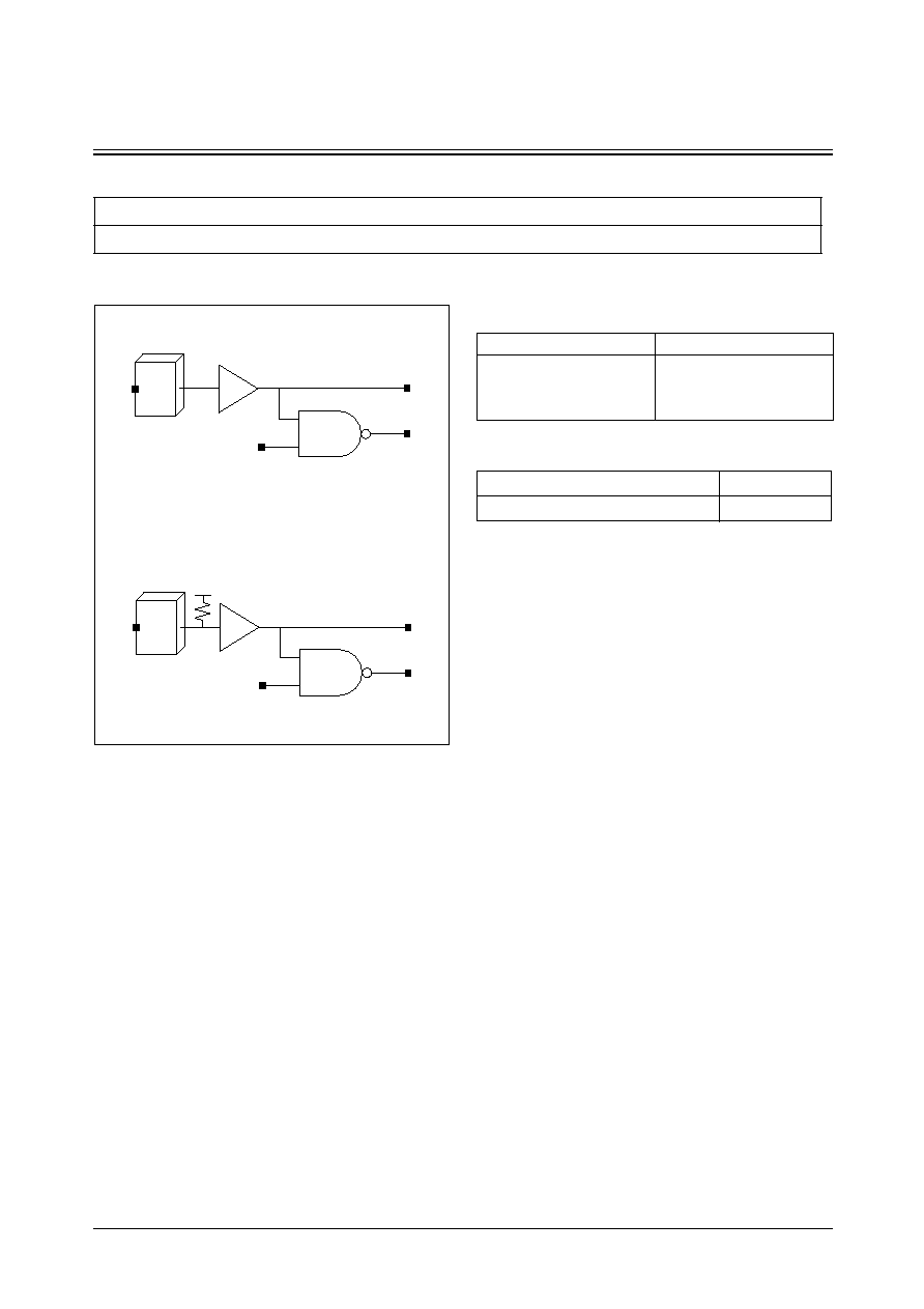
STDH90/MDL90
4-63
SEC ASIC
PHITATA/PHITU50ATA
ATA3 Input Buffers
Cell Availability
Logic Symbol
NOTE: These fail-safe I/O cells are available to receive signals from External devices without reducing reliability. How-
ever, if you want to use these fail-safe I/O cells, please contact to SEC ASIC first.
5V Interface
PHITATA/PHITU50ATA
Y
PO
PI
PAD
Y
PO
PI
PAD
PHITATA
PHITU50ATA
Truth Table
Standard Load (SL)
PAD
PI
Y
PO
1
1
1
0
0
x
0
1
1
0
1
1
Cell Name
PI
PHITATA/PHITU50ATA
2.3
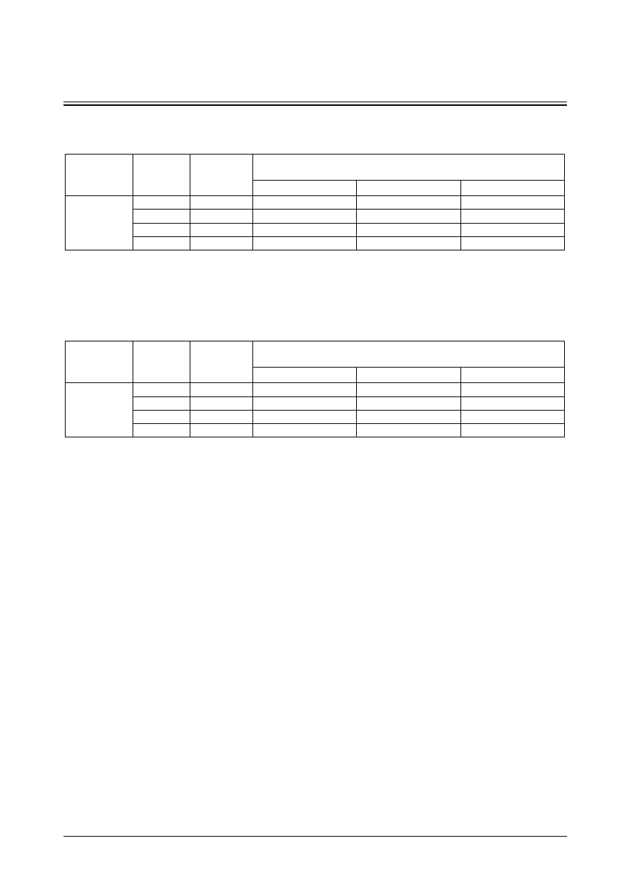
SEC ASIC
4-64
STDH90/MDL90
PHITATA/PHITU50ATA
ATA3 Input Buffers
PHITATA Switching Characteristics
[Delays for typical process, 25 C, 5.0V, when t , t = 0.80ns]
o
R F
(SL : Standard Load)
Path
Parameter
Delay [ns]
SL = 2
Delay Equations [ns]
Group1*
Group2*
Group3*
PAD to Y
tR
0.136
0.116 + 0.010*SL
0.113 + 0.011*SL
0.099 + 0.011*SL
tF
0.198
0.181 + 0.009*SL
0.180 + 0.009*SL
0.165 + 0.009*SL
tPLH
0.575
0.563 + 0.006*SL
0.566 + 0.005*SL
0.576 + 0.005*SL
tPHL
0.913
0.893 + 0.010*SL
0.912 + 0.006*SL
0.955 + 0.005*SL
*Group1 : SL < 4, *Group2 : 4 SL 46, *Group3 : 46 < SL
< <
= =
PHITU50ATA Switching Characteristics
[Delays for typical process, 25 C, 5.0V, when t , t = 0.80ns]
o
R F
(SL : Standard Load)
Path
Parameter
Delay [ns]
SL = 2
Delay Equations [ns]
Group1*
Group2*
Group3*
PAD to Y
tR
0.142
0.121 + 0.011*SL
0.120 + 0.011*SL
0.107 + 0.011*SL
tF
0.204
0.180 + 0.012*SL
0.197 + 0.008*SL
0.156 + 0.009*SL
tPLH
0.607
0.595 + 0.006*SL
0.598 + 0.005*SL
0.608 + 0.005*SL
tPHL
0.964
0.947 + 0.009*SL
0.959 + 0.006*SL
1.006 + 0.005*SL
*Group1 : SL < 4, *Group2 : 4 SL 46, *Group3 : 46 < SL
< <
= =
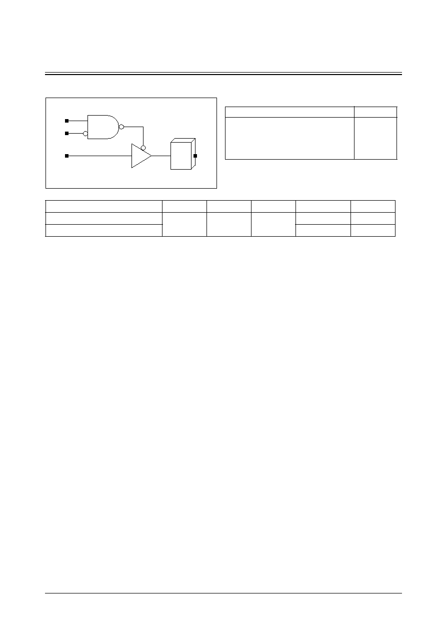
STDH90/MDL90
4-65
SEC ASIC
PHSOT12S1FATA/PHSOT4S1FATA
ATA3 Tri-State Output Buffers
Logic Symbol
Standard Load (SL)
NOTE: These fail-safe I/O cells are available to receive signals from External devices without reducing reliability. How-
ever, if you want to use these fail-safe I/O cells, please contact to SEC ASIC first.
Cell Name
TN
EN
A
IOH
IOL
PHSOT12S1FATA
2.1
2.4
5.7
1mA
12mA
PHSOT4S1FATA
1mA
4mA
PAD
A
TN
EN
Truth Table
TN
EN
A
PAD
1
0
0
0
1
0
1
1
x
1
x
Hi-Z
0
x
x
Hi-Z

SEC ASIC
4-66
STDH90/MDL90
PHSOT12S1FATA/PHSOT4S1FATA
ATA3 Tri-State Output Buffers
PHSOT12S1FATA Switching Characteristics
[Delays for typical process, 25 C, 5.0V, when t , t = 0.80ns]
o
R F
(CL : Capacitive Load[pf])
Path
Parameter
Delay [ns]
CL = 50.0pF
Delay Equations [ns]
Group1*
Group2*
Group3*
A to PAD
tR
27.206
0.648 + 0.531*CL
0.653 + 0.531*CL
0.650 + 0.531*CL
tF
2.007
0.181 + 0.037*CL
0.160 + 0.037*CL
0.154 + 0.037*CL
tPLH
12.377
1.637 + 0.215*CL
1.645 + 0.215*CL
1.636 + 0.215*CL
tPHL
3.323
1.749 + 0.031*CL
1.770 + 0.031*CL
1.776 + 0.031*CL
TN to PAD
tR
27.206
0.648 + 0.531*CL
0.653 + 0.531*CL
0.644 + 0.531*CL
tF
2.007
0.181 + 0.037*CL
0.168 + 0.037*CL
0.148 + 0.037*CL
tPLH
12.414
1.676 + 0.215*CL
1.658 + 0.215*CL
1.681 + 0.215*CL
tPHL
3.380
1.806 + 0.031*CL
1.819 + 0.031*CL
1.834 + 0.031*CL
tPLZ
1.529
1.529 + 0.000*CL
1.529 + 0.000*CL
1.529 + 0.000*CL
tPHZ
1.351
1.351 + 0.000*CL
1.351 + 0.000*CL
1.351 + 0.000*CL
EN to PAD
tR
27.206
0.648 + 0.531*CL
0.653 + 0.531*CL
0.644 + 0.531*CL
tF
2.007
0.181 + 0.037*CL
0.160 + 0.037*CL
0.154 + 0.037*CL
tPLH
12.703
1.963 + 0.215*CL
1.963 + 0.215*CL
1.963 + 0.215*CL
tPHL
3.670
2.096 + 0.031*CL
2.117 + 0.031*CL
2.117 + 0.031*CL
tPLZ
1.224
1.224 + 0.000*CL
1.224 + 0.000*CL
1.224 + 0.000*CL
tPHZ
1.018
1.018 + 0.000*CL
1.018 + 0.000*CL
1.018 + 0.000*CL
*Group1 : CL < 75, *Group2 : 75 CL 85, *Group3 : 85 < CL
< <
= =
PHSOT4S1FATA Switching Characteristics
[Delays for typical process, 25 C, 5.0V, when t , t = 0.80ns]
o
R F
(CL : Capacitive Load[pf])
Path
Parameter
Delay [ns]
CL = 50.0pF
Delay Equations [ns]
Group1*
Group2*
Group3*
A to PAD
tR
27.206
0.648 + 0.531*CL
0.653 + 0.531*CL
0.650 + 0.531*CL
tF
5.760
0.194 + 0.111*CL
0.203 + 0.111*CL
0.192 + 0.111*CL
tPLH
12.323
1.587 + 0.215*CL
1.589 + 0.215*CL
1.586 + 0.215*CL
tPHL
5.988
1.340 + 0.093*CL
1.337 + 0.093*CL
1.343 + 0.093*CL
TN to PAD
tR
27.206
0.648 + 0.531*CL
0.653 + 0.531*CL
0.644 + 0.531*CL
tF
5.761
0.199 + 0.111*CL
0.187 + 0.111*CL
0.198 + 0.111*CL
tPLH
12.360
1.624 + 0.215*CL
1.611 + 0.215*CL
1.625 + 0.215*CL
tPHL
6.052
1.404 + 0.093*CL
1.386 + 0.093*CL
1.403 + 0.093*CL
tPLZ
1.380
1.380 + 0.000*CL
1.380 + 0.000*CL
1.380 + 0.000*CL
tPHZ
1.351
1.351 + 0.000*CL
1.351 + 0.000*CL
1.351 + 0.000*CL
EN to PAD
tR
27.206
0.648 + 0.531*CL
0.653 + 0.531*CL
0.644 + 0.531*CL
tF
5.761
0.199 + 0.111*CL
0.187 + 0.111*CL
0.198 + 0.111*CL
tPLH
12.650
1.914 + 0.215*CL
1.916 + 0.215*CL
1.913 + 0.215*CL
tPHL
6.342
1.694 + 0.093*CL
1.691 + 0.093*CL
1.697 + 0.093*CL
tPLZ
1.083
1.083 + 0.000*CL
1.083 + 0.000*CL
1.083 + 0.000*CL
tPHZ
1.018
1.018 + 0.000*CL
1.018 + 0.000*CL
1.018 + 0.000*CL
*Group1 : CL < 75, *Group2 : 75 CL 85, *Group3 : 85 < CL
< <
= =

STDH90/MDL90
4-67
SEC ASIC
PHSBTT4S1FATA/PHSBTT12S1FATA
ATA3 Tri-State Bidirectional Buffer
Logic Symbol
NOTE: These fail-safe I/O cells are available to receive signals from External devices without reducing reliability. How-
ever, if you want to use these fail-safe I/O cells, please contact to SEC ASIC first.
PAD
A
TN
EN
Y
PO
PI
Truth Table
Input Truth Table
Output Truth Table
PAD
PI
Y
PO
1
1
1
0
0
x
0
1
1
0
1
1
A
EN
TN
PAD
0
0
1
0
1
0
1
1
x
1
x
Hi-Z
x
x
0
Hi-Z
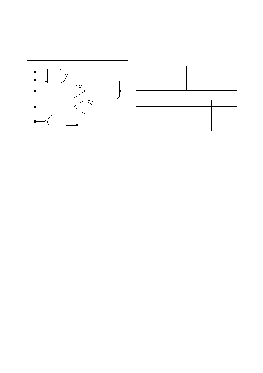
SEC ASIC
4-68
STDH90/MDL90
PHSBTU50T4S1FATA/PHSBTU50T12S1FATA
ATA3 Tri-State Bidirectional Buffer with 50K Pull-Up
Logic Symbol
NOTE: These fail-safe I/O cells are available to receive signals from External devices without reducing reliability. How-
ever, if you want to use these fail-safe I/O cells, please contact to SEC ASIC first.
PAD
A
TN
EN
Y
PO
PI
Truth Table
Input Truth Table
Output Truth Table
PAD
PI
Y
PO
1
1
1
0
0
x
0
1
1
0
1
1
A
EN
TN
PAD
0
0
1
0
1
0
1
1
x
1
x
Hi-Z
x
x
0
Hi-Z

STDH90/MDL90
4-69
SEC ASIC
I/O with unbalanced output impedance
Cell List
Cell Name
Function Description
PHOT24S4F
Unbalanced Tri-State Output Buffer
PHBTT24S4F
Unbalanced Tri-State Bi-Directional Buffer
PHBTU50CT24S4F
Unbalanced Tri-State Bi-Directional Buffer with Controlled Pull-Up
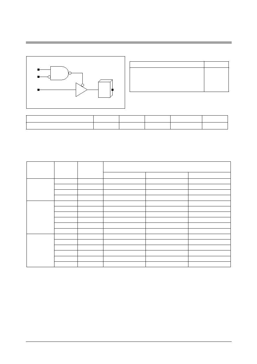
SEC ASIC
4-70
STDH90/MDL90
PHOT24S4F
Unbalanced Tri-State Output Buffer
Logic Symbol
Standard Load (SL)
Cell Name
TN
EN
A
IOH
IOL
PHOT24S4F
2.1
2.4
5.7
4mA
24mA
PAD
A
TN
EN
PHOT24S4F Switching Characteristics
[Delays for typical process, 25 C, 5.0V, when t , t = 0.80ns]
o
R F
(CL : Capacitive Load[pf])
Path
Parameter
Delay [ns]
CL = 50.0pF
Delay Equations [ns]
Group1*
Group2*
Group3*
A to PAD
tR
10.734
0.430 + 0.206*CL
0.436 + 0.206*CL
0.430 + 0.206*CL
tF
2.178
0.766 + 0.028*CL
0.776 + 0.028*CL
0.774 + 0.028*CL
tPLH
6.073
1.323 + 0.095*CL
1.323 + 0.095*CL
1.329 + 0.095*CL
tPHL
3.014
2.090 + 0.018*CL
2.171 + 0.017*CL
2.205 + 0.017*CL
TN to PAD
tR
10.735
0.433 + 0.206*CL
0.436 + 0.206*CL
0.430 + 0.206*CL
tF
2.178
0.766 + 0.028*CL
0.776 + 0.028*CL
0.768 + 0.028*CL
tPLH
6.102
1.350 + 0.095*CL
1.345 + 0.095*CL
1.360 + 0.095*CL
tPHL
3.157
2.235 + 0.018*CL
2.290 + 0.018*CL
2.350 + 0.017*CL
tPLZ
1.666
1.666 + 0.000*CL
1.666 + 0.000*CL
1.666 + 0.000*CL
tPHZ
1.407
1.407 + 0.000*CL
1.407 + 0.000*CL
1.407 + 0.000*CL
EN to PAD
tR
10.734
0.430 + 0.206*CL
0.436 + 0.206*CL
0.430 + 0.206*CL
tF
2.178
0.764 + 0.028*CL
0.785 + 0.028*CL
0.774 + 0.028*CL
tPLH
6.384
1.632 + 0.095*CL
1.643 + 0.095*CL
1.611 + 0.095*CL
tPHL
3.448
2.526 + 0.018*CL
2.597 + 0.017*CL
2.639 + 0.017*CL
tPLZ
1.350
1.348 + 0.000*CL
1.351 + 0.000*CL
1.351 + 0.000*CL
tPHZ
1.103
1.103 + 0.000*CL
1.100 + 0.000*CL
1.100 + 0.000*CL
*Group1 : CL < 75, *Group2 : 75 CL 85, *Group3 : 85 < CL
< <
= =
Truth Table
TN
EN
A
PAD
1
0
0
0
1
0
1
1
x
1
x
Hi-Z
0
x
x
Hi-Z
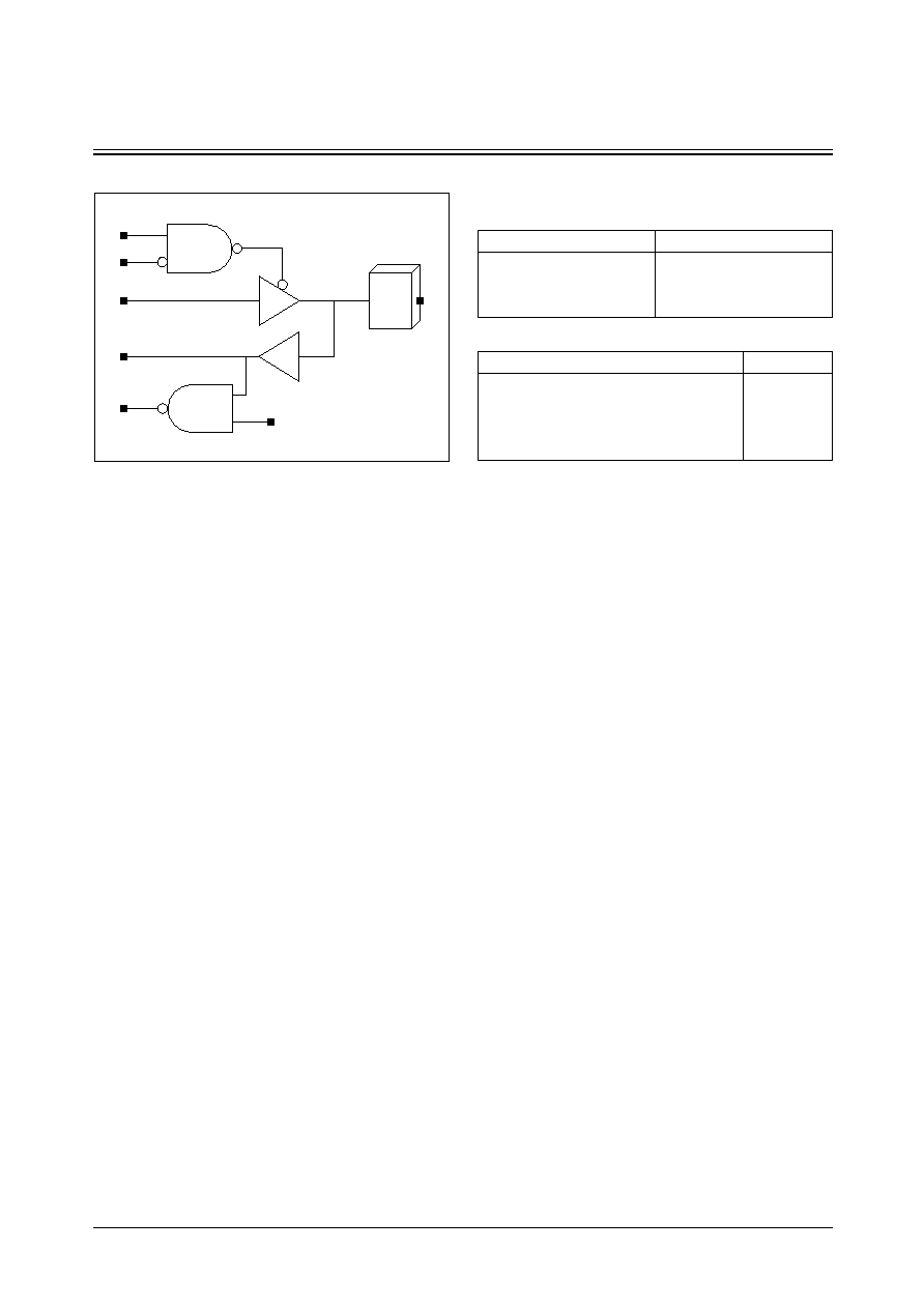
STDH90/MDL90
4-71
SEC ASIC
PHBTT24S4F
Unbalanced Tri-State Bidirectional Buffer
Logic Symbol
PAD
A
TN
EN
Y
PO
PI
Truth Table
Input Truth Table
Output Truth Table
PAD
PI
Y
PO
1
1
1
0
0
x
0
1
1
0
1
1
A
EN
TN
PAD
0
0
1
0
1
0
1
1
x
1
x
Hi-Z
x
x
0
Hi-Z
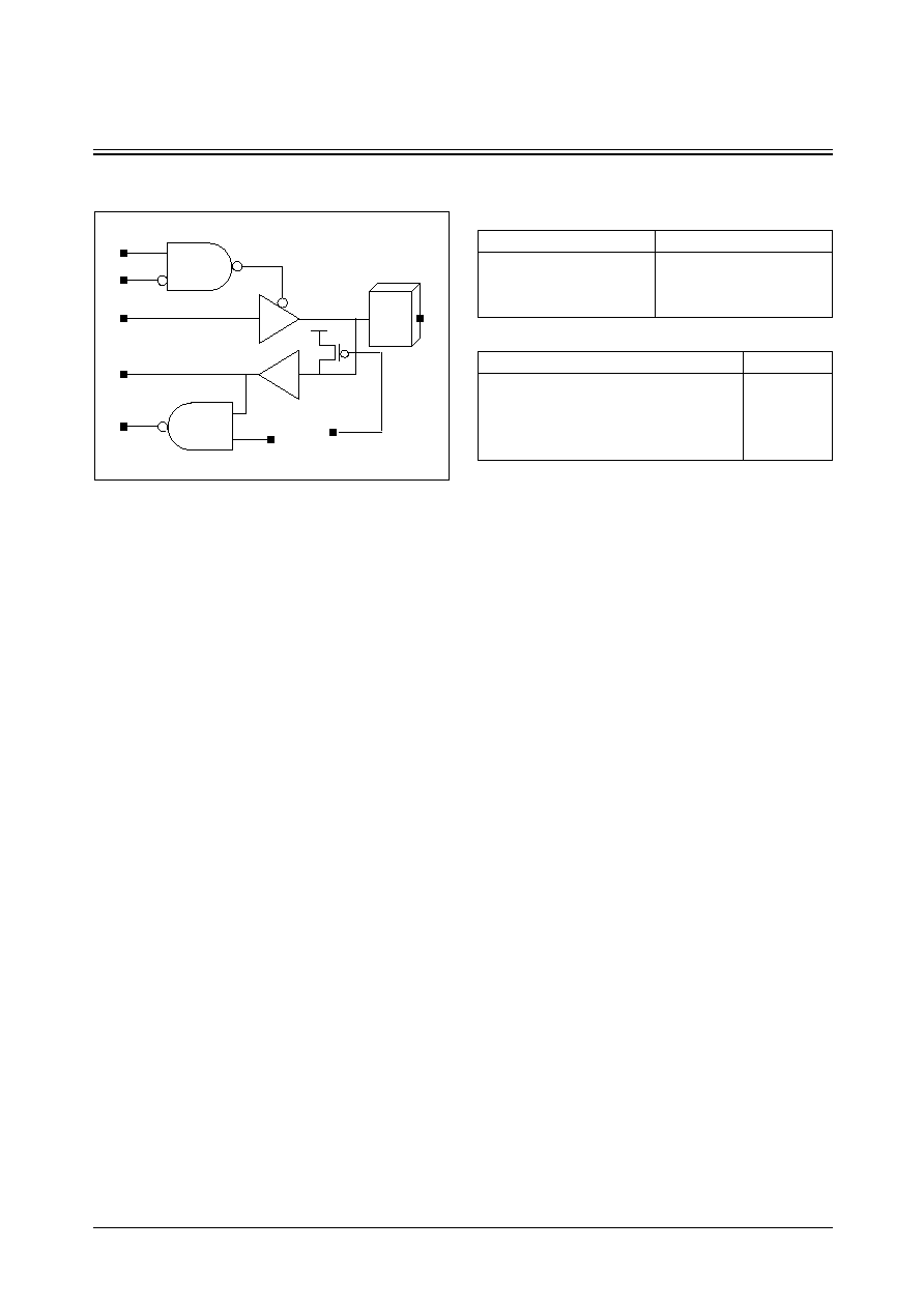
SEC ASIC
4-72
STDH90/MDL90
PHBTU50CT24S4F
Unbalanced Tri-State Bidirectional Buffer with Controlled Pull-Up
Logic Symbol
PAD
A
TN
EN
Y
PO
PI
PUC
50K
Truth Table
Input Truth Table
Output Truth Table
PAD
PI
Y
PO
1
1
1
0
0
x
0
1
1
0
1
1
A
EN
TN
PAD
0
0
1
0
1
0
1
1
x
1
x
Hi-Z
x
x
0
Hi-Z

STDH90/MDL90
4-73
SEC ASIC
I/O with controlled pull-up
Cell List
Cell Name
Function Description
PHITU50C
Controlled Input Buffer
PHBTU50CD2
Controlled Open Drain Bi-Directional Buffers
PHBTU50CD4
PHBTU50CT2
Controlled Tri-State Bi-Directional Buffers
PHBTU50CT4
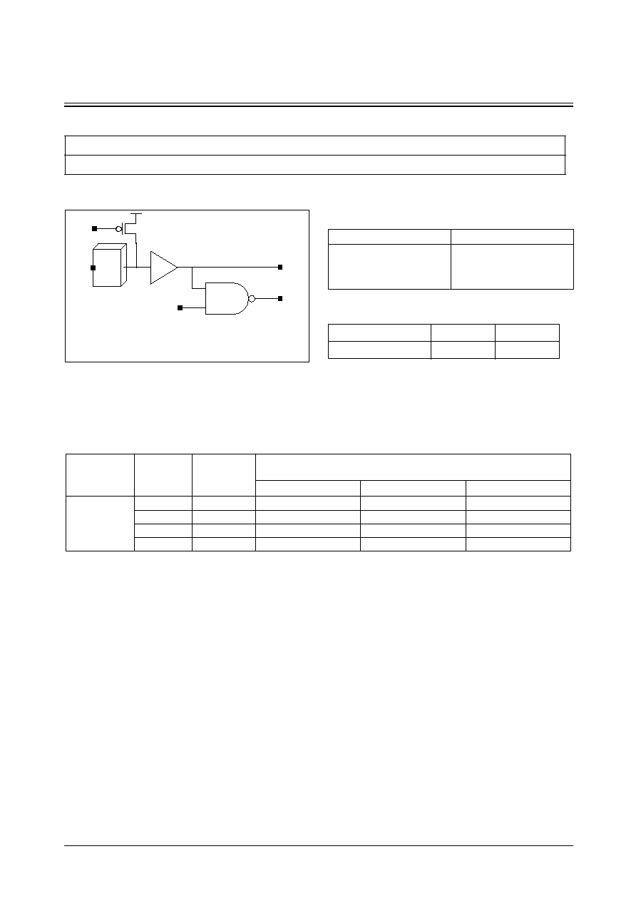
SEC ASIC
4-74
STDH90/MDL90
PHITU50C
Controlled Input Buffer
Cell Availability
Logic Symbol
5V Interface
PHITU50C
Y
PO
PI
PAD
PHITU50C
PUC
50K
PHITU50C Switching Characteristics
[Delays for typical process, 25 C, 5.0V, when t , t = 0.80ns]
o
R F
(SL : Standard Load)
Path
Parameter
Delay [ns]
SL = 2
Delay Equations [ns]
Group1*
Group2*
Group3*
PAD to Y
tR
0.139
0.115 + 0.012*SL
0.121 + 0.011*SL
0.106 + 0.011*SL
tF
0.197
0.180 + 0.008*SL
0.178 + 0.009*SL
0.163 + 0.009*SL
tPLH
0.558
0.546 + 0.006*SL
0.549 + 0.005*SL
0.560 + 0.005*SL
tPHL
0.939
0.922 + 0.008*SL
0.933 + 0.006*SL
0.978 + 0.005*SL
*Group1 : SL < 4, *Group2 : 4 SL 46, *Group3 : 46 < SL
< <
= =
Truth Table
Standard Load (SL)
PAD
PI
Y
PO
1
1
1
0
0
x
0
1
1
0
1
1
Cell Name
PI
PUC
PHITU50C
2.3
6
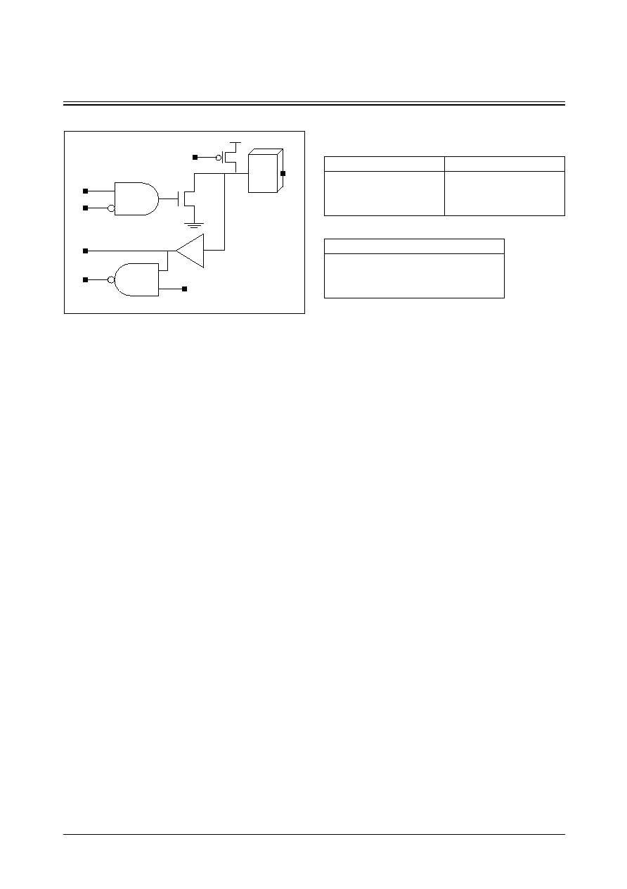
STDH90/MDL90
4-75
SEC ASIC
PHBTU50CD2/PHBTU50CD4
Controlled Open Drain Bidirectional Buffer
Logic Symbol
PAD
TN
EN
Y
PO
PI
PUC
50K
Truth Table
Input Truth Table
Output Truth Table
PAD
PI
Y
PO
1
1
1
0
0
x
0
1
1
0
1
1
EN
TN
PAD
0
1
0
1
x
Hi-Z
x
0
Hi-Z
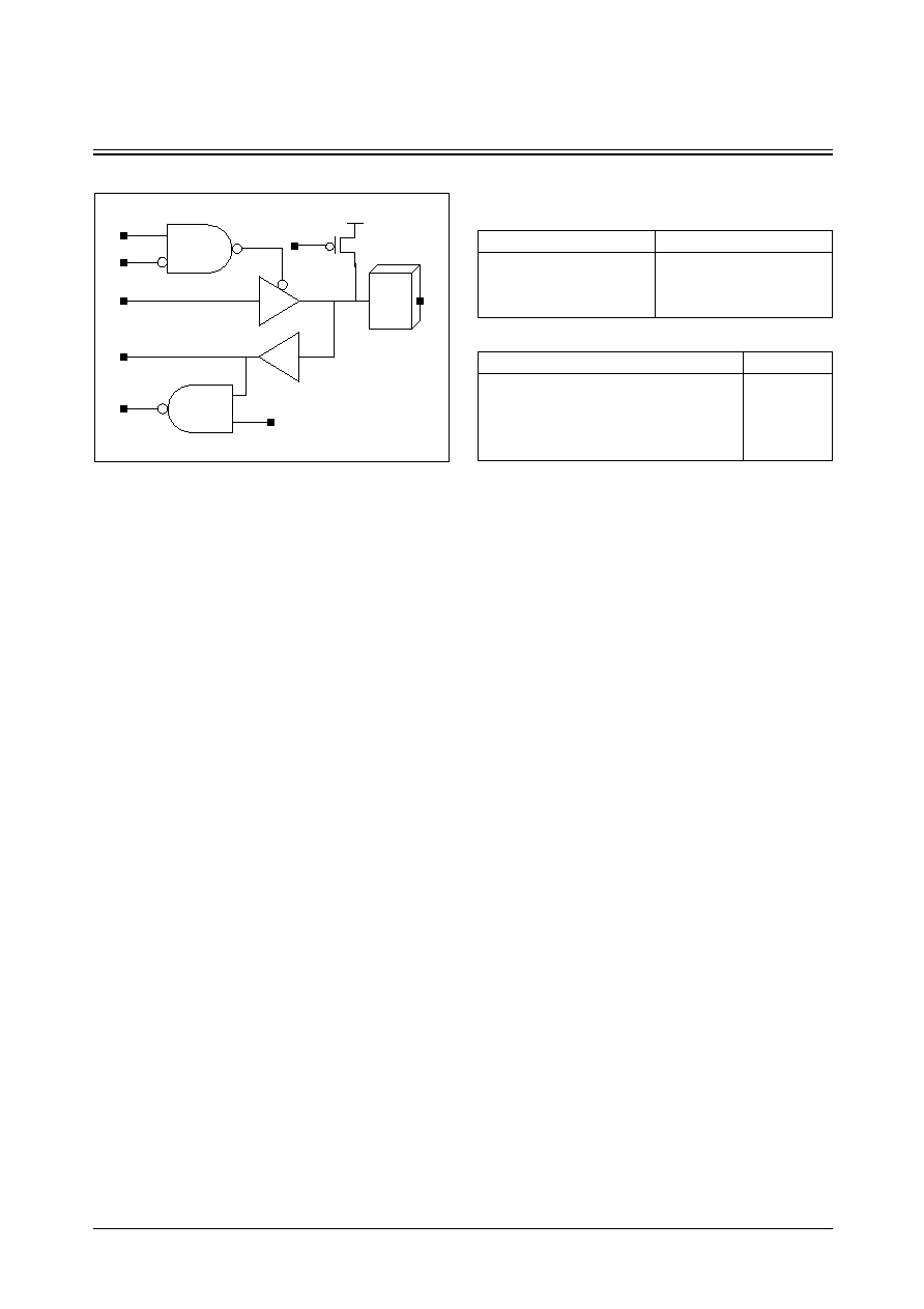
SEC ASIC
4-76
STDH90/MDL90
PHBTU50CT2/PHBTU50CT4
Controlled Tri-State Bidirectional Buffer
Logic Symbol
PAD
A
TN
EN
Y
PO
PI
PUC
50K
Truth Table
Input Truth Table
Output Truth Table
PAD
PI
Y
PO
1
1
1
0
0
x
0
1
1
0
1
1
A
EN
TN
PAD
0
0
1
0
1
0
1
1
x
1
x
Hi-Z
x
x
0
Hi-Z
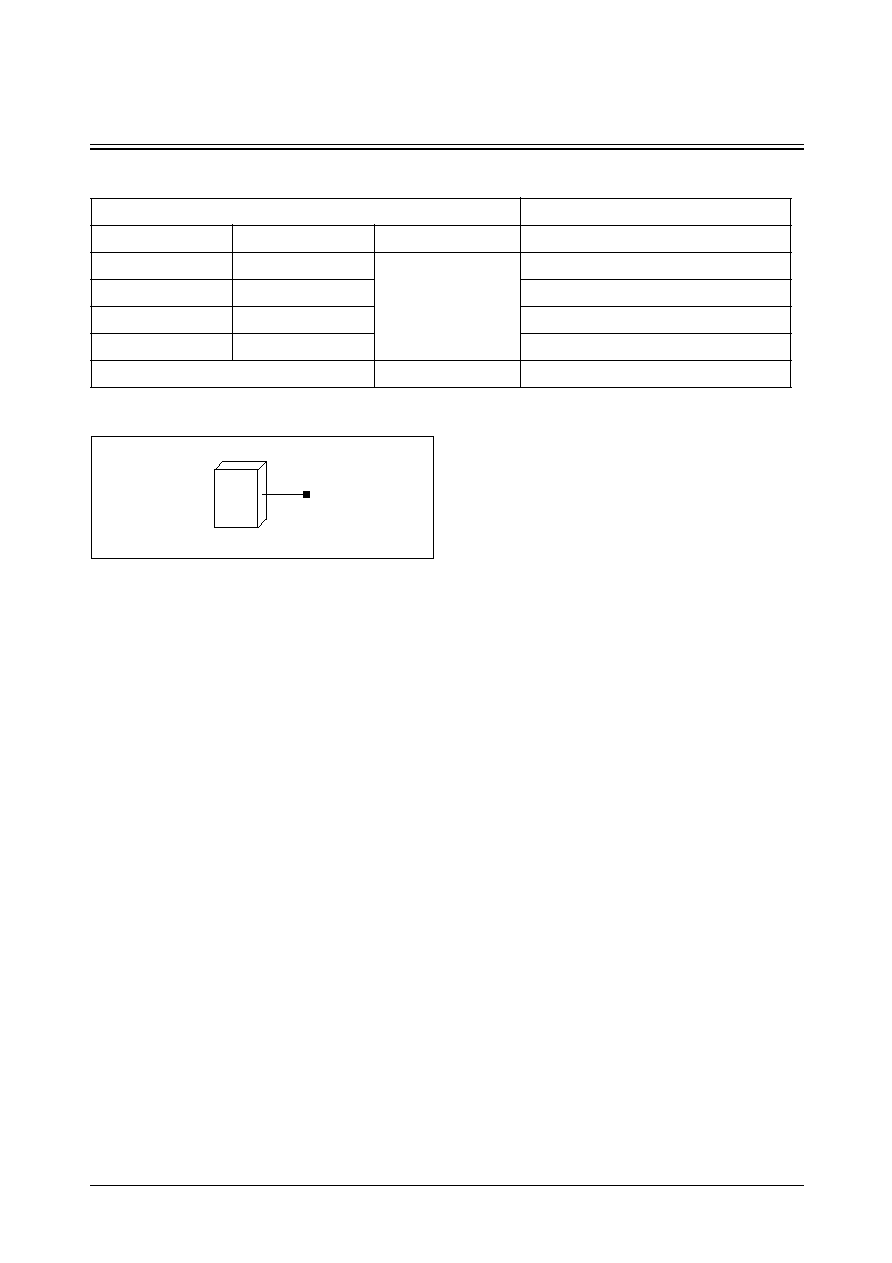
SEC ASIC
4-77
STDH90/MDL90
POWER PADS
Cell List
Logic Symbol
Cell Name
Function Description
VDD Pads
VSS Pads
VBB Pad
VDD3I
VSSI
3.3V Internal
VDD5P
VSSP
5V Pre-Driver
VDD5O
VSSO
5V Output-Driver
VDD5OP
VSSOP
5V Pre-Driver and Output-Driver
VBB
Bulk(P-substrate)
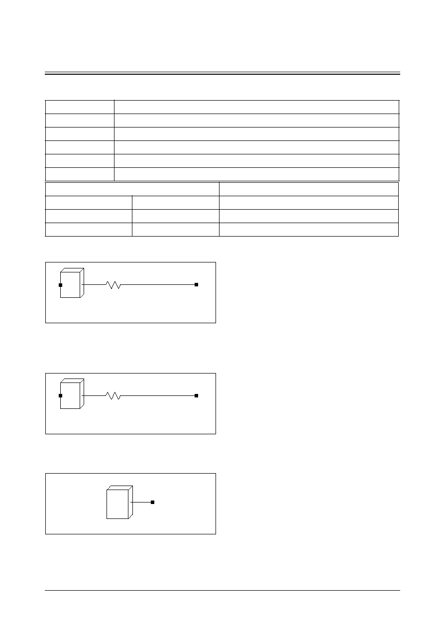
STDH90/MDL90
4-78
SEC ASIC
ANALOG INTERFACE
Cell List
Logic Symbol I(Input Pad)
Logic Symbol II(Output Pad)
Logic Symbol III(Power Pad)
Cell Name
Function Description
PICA
Analog Normal Input Pad with Separate Bulk Bias
PICA_10
Analog Normal Input Pad with Resistor 10ohm and Separate Bulk Bias
PICA_25
Analog Normal Input Pad with Resistor 25ohm and Separate Bulk Bias
PICA_500
Analog Normal Input Pad with Resistor 500ohm and Separate Bulk Bias
POBA
Analog Normal Output Pad with Separate Bulk Bias
Cell Name
Function Description
VDD Power Pads
VSS Power Pads
VCCA
Analog 3.3V Power with Separate Bulk Bias
VSSA
Analog Ground with Separate Bulk Bias
Y
PAD
A
PAD
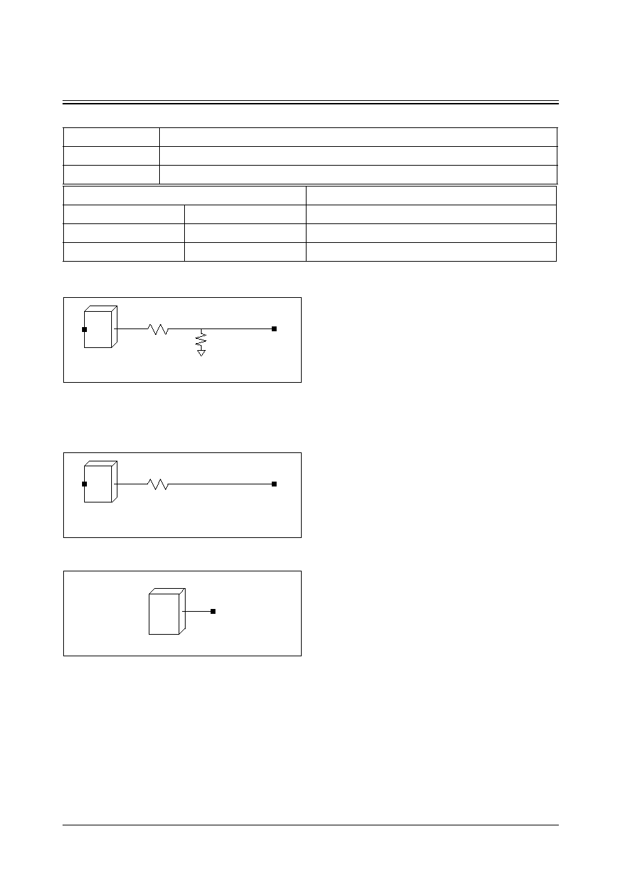
STDH90/MDL90
4-79
SEC ASIC
DRAM INTERFACE
Cell List
Logic Symbol I(Input Pad)
Logic Symbol II(Output Pad)
Logic Symbol III(Power Pad)
Cell Name
Function Description
DCPAD_PD50K
DRAM DC Input Pad with 50K Pull-Up
DCPAD
DRAM DC Output Pad
Cell Name
Function Description
VDD Power Pads
VSS Power Pads
VCCD
DRAM 3.3V Power with Separate Bulk Bias
VSSD
DRAM Ground with Separate Bulk Bias
Y
PAD
50K
A
PAD

SEC ASIC
4-80
STDH90/MDL90
Customized I/O
Cell List
Cell Name
Function Description
PHOTI4
Tri-State Output Inverter
PHBTTI4
Tri-State Bi-Directional I/O with Inverting Output
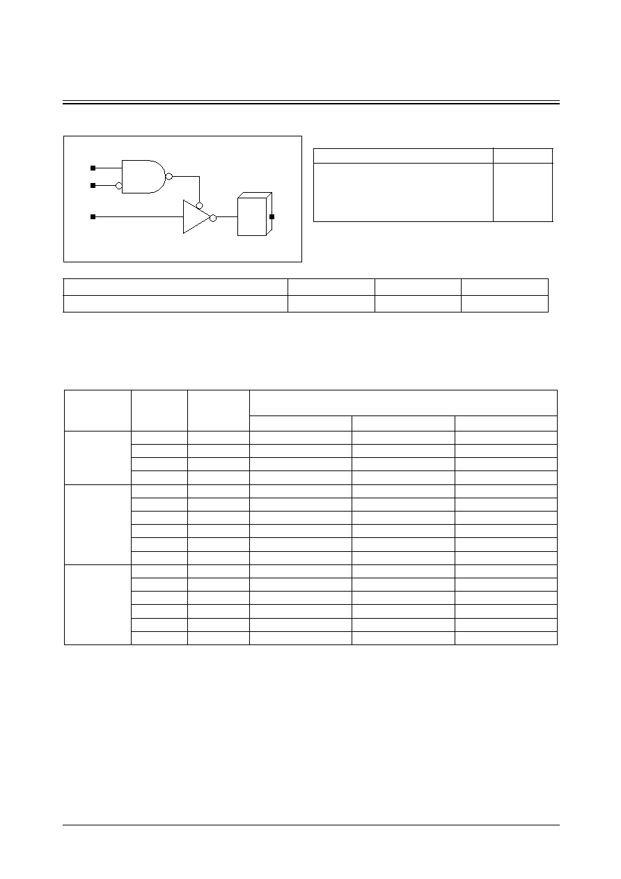
STDH90/MDL90
4-81
SEC ASIC
PHOTI4
Tri-State Output Inverter
Logic Symbol
Standard Load (SL)
Cell Name
TN
EN
A
PHOTI4
2.1
2.4
5.7
PAD
A
TN
EN
PHOTI4 Switching Characteristics
[Delays for typical process, 25 C, 5.0V, when t , t = 0.80ns]
o
R F
(CL : Capacitive Load[pf])
Path
Parameter
Delay [ns]
CL = 50.0pF
Delay Equations [ns]
Group1*
Group2*
Group3*
A to PAD
tR
10.735
0.433 + 0.206*CL
0.436 + 0.206*CL
0.430 + 0.206*CL
tF
9.310
0.398 + 0.178*CL
0.401 + 0.178*CL
0.395 + 0.178*CL
tPLH
6.041
1.297 + 0.095*CL
1.295 + 0.095*CL
1.293 + 0.095*CL
tPHL
6.062
1.424 + 0.093*CL
1.421 + 0.093*CL
1.427 + 0.093*CL
TN to PAD
tR
10.734
0.430 + 0.206*CL
0.436 + 0.206*CL
0.430 + 0.206*CL
tF
9.310
0.398 + 0.178*CL
0.401 + 0.178*CL
0.395 + 0.178*CL
tPLH
6.063
1.317 + 0.095*CL
1.311 + 0.095*CL
1.322 + 0.095*CL
tPHL
6.087
1.449 + 0.093*CL
1.446 + 0.093*CL
1.452 + 0.093*CL
tPLZ
1.385
1.385 + 0.000*CL
1.385 + 0.000*CL
1.385 + 0.000*CL
tPHZ
1.407
1.407 + 0.000*CL
1.407 + 0.000*CL
1.407 + 0.000*CL
EN to PAD
tR
10.735
0.433 + 0.206*CL
0.436 + 0.206*CL
0.430 + 0.206*CL
tF
9.310
0.398 + 0.178*CL
0.401 + 0.178*CL
0.395 + 0.178*CL
tPLH
6.345
1.599 + 0.095*CL
1.600 + 0.095*CL
1.581 + 0.095*CL
tPHL
6.378
1.740 + 0.093*CL
1.737 + 0.093*CL
1.743 + 0.093*CL
tPLZ
1.064
1.064 + 0.000*CL
1.064 + 0.000*CL
1.064 + 0.000*CL
tPHZ
1.103
1.103 + 0.000*CL
1.100 + 0.000*CL
1.100 + 0.000*CL
*Group1 : CL < 75, *Group2 : 75 CL 85, *Group3 : 85 < CL
< <
= =
Truth Table
TN
EN
A
PAD
1
0
0
1
1
0
1
0
x
1
x
Hi-Z
0
x
x
Hi-Z
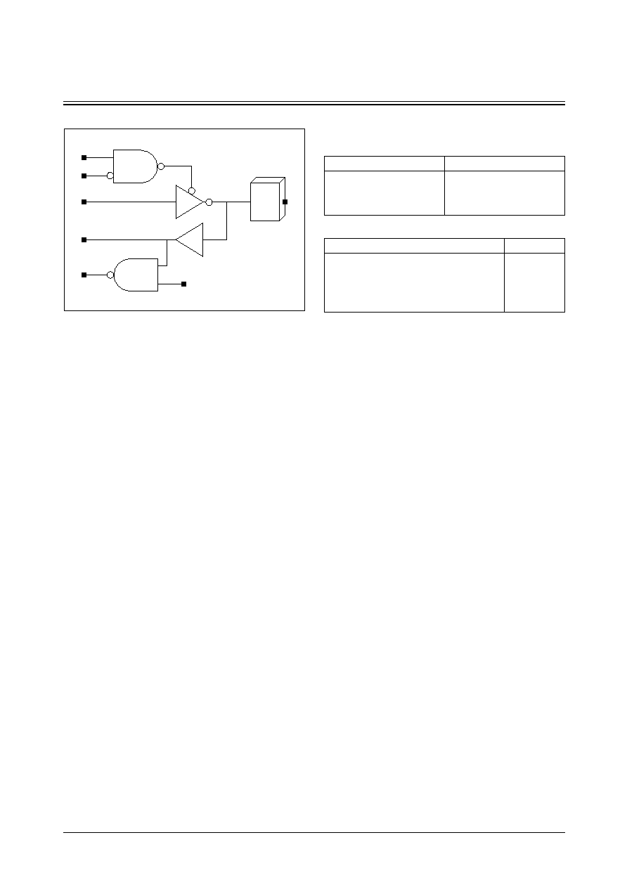
SEC ASIC
4-82
STDH90/MDL90
PHBTTI4
Tri-State Bidirectional I/O with Inverting Output
Logic Symbol
PAD
A
TN
EN
Y
PO
PI
Truth Table
Input Truth Table
Output Truth Table
PAD
PI
Y
PO
1
1
1
0
0
x
0
1
1
0
1
1
A
EN
TN
PAD
0
0
1
1
1
0
1
0
x
1
x
Hi-Z
x
x
0
Hi-Z

5
Compiled Macrocells
(Refer to STD90/MDL90)

6
PLL
(Refer to STD90/MDL90)

7
JTAG Boundary Scans
(Refer to STD90/MDL90)