 | –≠–ª–µ–∫—Ç—Ä–æ–Ω–Ω—ã–π –∫–æ–º–ø–æ–Ω–µ–Ω—Ç: STDL130 | –°–∫–∞—á–∞—Ç—å:  PDF PDF  ZIP ZIP |
Document Outline
- ˛ˇ
- ˛ˇ
- ˛ˇ
- ˛ˇ
- ˛ˇ
- ˛ˇ
- ˛ˇ
- ˛ˇ
- ˛ˇ
- ˛ˇ
- ˛ˇ
- ˛ˇ
- ˛ˇ
- ˛ˇ
- ˛ˇ
- ˛ˇ
- ˛ˇ
- ˛ˇ
- ˛ˇ

Revision History (Based on Hard Copy).
- 1'st Edition(V1.0) : April. 2003
∑ Chapter 1 : Introduction
∑ Chapter 2 : DC Electrical Characteristics(Recommended Operating Conditions)
∑ Chapter 3 : Primitive Cells
∑ Chapter 5 : Compiled Memories

STDL130
0.18
µ
m 1.8V CMOS Standard Cell Library
for Pure Logic Products

STDL130
0.18
µ
m 1.8V CMOS Standard Cell Library
for Pure Logic Products
Data Book
Copyright
2003, 2002 by Samsung Electronics Co., Ltd.
All rights reserved. No part of this document may be reproduced, in any form or by any means, without the prior
written consent of the publisher. Samsung assumes no responsibility for any errors resulting from the use of the
information contained herein, nor does it convey any license under the patent rights of Samsung or others.
Samsung reserves the right to make changes in its products or product specification to improve function or design
at any time, without notice.
SEC and STDL130 are trademarks of Samsung Electronics Co., Ltd. Verilog is a registered trademark of Cadence
Design Systems, Inc. Viewlogic is a registered trademark of Viewlogic Systems, Inc. Mentor is a registered
trademark or Mentor Graphics Co. Synopsys is a registered trademark of Synopsys, Inc.
Head Office
Samsung Electronics Co., Ltd
System LSI Business,
ASIC Infro P/J
San #24, Nongseo-Ri,
Giheung-Eup, Yongin-City,
Gyunggi-Do, Korea
449-711
TEL
82-31-209-6500, 6501 (Hot Line)
FAX
82-31-209-4920
http://www.samsung.com/Products/Semiconductor/
ASIC
Printed in the Republic of Kore
Marketing Team
Samsung Electronics Co., Ltd
System LSI Business,
Sales and Marketing Team
San #24, Nongseo-Ri,
Giheung-Eup, Yongin-City,
Gyunggi-Do, Korea
TEL
82-2-31-209-1940
FAX
82-2-31-209-1919

Samsung ASIC
iv
STDL130
Introduction
This databook contains information about STDL130 0.18
µ
m 1.8V standard cell library for pure Logic
products developed by SEC (Samsung Electronics Corporation).
The "library" basically contains various kinds of primitive and I/O cells and cores which are used for
developing ASIC (Application Specific Integrated Circuit). It also includes a design kit helping designers to
work in a workstation platform, and all sorts of design environments needed for an automatic chip design.
There are six chapters in this databook:
Chapter 1
Introduction
Chapter 2
Electrical Characteristics
Chapter 3
Primitives Cells
Chapter 4
Input/Output Cells
Chapter 5
Compiled Memories
Chapter 6
PLL
Appendix A
Glossary of Analog Terms
Appendix B
Timings
Appendix C
Maximum Fanouts
Appendix D
Package Capabilities
In this databook, each cell is followed by its AC electrical characteristics, and these characteristic values are
almost equal when the corresponding cell is operated in a real chip.
The purpose of this databook is to prevent any misuse or misapplication of STDL130 cell library by providing
precise information about the cell list, electrical data, directions for use, and matters demanding special
attention.
If you want to get more information about digital cores and analog cores that are not included in this databook,
access the Samsung ASIC web site(http://www.samsung.com/Products/Semiconductor/ASIC) or contact
head office.

Samsung ASIC
v
STDL130
Contents
1
Introduction
1.1 Library Description ................................................................................................................1-1
1.2 Features ................................................................................................................................1-2
1.3 EDA Support .........................................................................................................................1-4
1.4 Product Family ......................................................................................................................1-4
1.4.1 Analog Cores ...............................................................................................................1-4
1.4.2 Primitive Cells ..............................................................................................................1-8
1.4.3 Compiled Memories.....................................................................................................1-9
1.4.4 Input/Output Cells ........................................................................................................1-11
1.5
Timings .................................................................................................................................1-14
1.6
Design for Test (DFT) Methodology......................................................................................1-22
1.7
Maximum Fanouts ................................................................................................................1-25
1.8
Packages Capability by Pitch and Lead Count .....................................................................1-32
1.9
Power Dissipation .................................................................................................................1-33
1.10 V
DD
/V
SS
Rules and Guidelines.............................................................................................1-37
1.11 Crystal Oscillator Considerations .........................................................................................1-45
2
Electrical Characteristics
DC Electrical Characteristics.........................................................................................................2-1
3
Primitive Cells
Overview .......................................................................................................................................3-1
Summary Tables ...........................................................................................................................3-2
Primitive Cells
AD2_LP/AD2D2_LP/AD2D4_LP/AD2D8_LP ................................................................................3-14
AD2B_LP/AD2BD2_LP/AD2BD4_LP/AD2BD8_LP ......................................................................3-16
AD3_LP/AD3D2_LP/AD3D4_LP ...................................................................................................3-18
AD4_LP/AD4D2_LP/AD4D4_LP ...................................................................................................3-20
AD5_LP/AD5D2_LP/AD5D4_LP ...................................................................................................3-22
ND2_LP/ND2D2_LP/ND2D4_LP/ND2D8_LP ...............................................................................3-25
ND2B_LP/ND2BD2_LP/ND2BD4_LP/ND2BD8_LP......................................................................3-27
ND3_LP/ND3D2_LP/ND3D4_LP ..................................................................................................3-29
ND3B_LP/ND3BD2_LP/ND3BD4_LP/ND2BD8_LP......................................................................3-32
ND4_LP/ND4D2_LP/ND4D4_LP ..................................................................................................3-35

STDL130
vi
Samsung ASIC
Contents
ND5_LP/ND5D2_LP/ND5D4_LP ..................................................................................................3-37
ND6_LP/ND6D2_LP/ND6D4_LP ..................................................................................................3-40
ND8_LP/ND8D2_LP/ND8D4_LP ..................................................................................................3-44
NR2_LP/NR2D2_LP/NR2D4_LP/NR2D8_LP/NR2A_LP ..............................................................3-48
NR2B_LP/NR2BD2_LP/NR2BD4_LP/NR2BD8_LP......................................................................3-50
NR3_LP/NR3D2_LP/NR3D4_LP/NR3A_LP .................................................................................3-52
NR4_LP/NR4D2_LP/NR4D4_LP ..................................................................................................3-55
NR5_LP/NR5D2_LP/NR5D4_LP ..................................................................................................3-57
NR6_LP/NR6D2_LP/NR6D4_LP ..................................................................................................3-61
NR8_LP/NR8D2_LP/NR8D4_LP ..................................................................................................3-65
OR2_LP/OR2D2_LP/OR2D4_LP/OR2D8_LP ..............................................................................3-69
OR2B_LP/OR2BD2_LP/OR2BD4_LP/OR2BD8_LP.....................................................................3-71
OR3_LP/OR3D3_LP/OR3D4_LP..................................................................................................3-73
OR4_LP/OR4D2_LP/OR4D4_LP..................................................................................................3-75
OR5_LP/OR5D2_LP/OR5D4_LP..................................................................................................3-77
XN2_LP/XN2D2_LP/XN2D4_LP ...................................................................................................3-80
XN3_LP/XN3D2_LP/XN3D4_LP ...................................................................................................3-82
XO2_LP/XO2D2_LP/XO2D4_LP ..................................................................................................3-84
XO3_LP/XO3D2_LP/XO3D4_LP ..................................................................................................3-86
AO21_LP/AO21D2_LP/AO21D4_LP.............................................................................................3-88
AO211_LP/AO211D2_LP/AO211D4_LP.......................................................................................3-90
AO2111_LP/AO2111D2_LP..........................................................................................................3-92
AO22_LP/AO22D2_LP/AO22D4_LP.............................................................................................3-94
AO22A_LP ....................................................................................................................................3-96
AO221_LP/AO221D2_LP/AO221D4_LP.......................................................................................3-97
AO222_LP/AO222D2_LP/AO222D4_LP.......................................................................................3-100
AO222A_LP ..................................................................................................................................3-104
AO2222D2_LP/AO2222D4_LP .....................................................................................................3-105
AO31_LP/AO31D2_LP/AO31D4_LP.............................................................................................3-109
AO311_LP.....................................................................................................................................3-111
AO3111_LP...................................................................................................................................3-112
AO32_LP/AO32D2_LP/AO32D4_LP.............................................................................................3-113
AO321_LP.....................................................................................................................................3-115
AO322_LP.....................................................................................................................................3-116
AO33_LP.......................................................................................................................................3-118
AO331_LP.....................................................................................................................................3-120
AO332_LP.....................................................................................................................................3-122
OA21_LP/OA21D2_LP/OA21D4_LP.............................................................................................3-124
OA211_LP/OA211D2_LP/OA211D4_LP.......................................................................................3-126
OA2111_LP/OA2111D2_LP..........................................................................................................3-128
OA22_LP/OA22D2_LP/OA22D4_LP.............................................................................................3-130
OA22A_LP/OA22D2A_LP/OA22D4A_LP .....................................................................................3-132
OA221_LP/OA221D2_LP/OA221D4_LP.......................................................................................3-134

Samsung ASIC
vii
STDL130
Contents
OA222_LP/OA222D2_LP/OA222D4_LP.......................................................................................3-137
OA2222_LP/OA2222D2_LP/OA2222D4_LP.................................................................................3-141
OA31_LP/OA31D2_LP/OA31D4_LP.............................................................................................3-145
OA311_LP.....................................................................................................................................3-147
OA3111_LP...................................................................................................................................3-148
OA32_LP.......................................................................................................................................3-149
OA321_LP.....................................................................................................................................3-150
OA322_LP.....................................................................................................................................3-151
OA33_LP.......................................................................................................................................3-153
SCG1_LP/SCG1D2_LP ................................................................................................................3-154
SCG2_LP/SCG2D2_LP/SCG2D4_LP...........................................................................................3-157
SCG3_LP/SCG3D2_LP/SCG3D4_LP...........................................................................................3-159
SCG4_LP/SCG4D2_LP/SCG4D4_LP...........................................................................................3-162
SCG5_LP/SCG5D2_LP/SCG5D4_LP...........................................................................................3-166
SCG6_LP/SCG6D2_LP ................................................................................................................3-170
SCG7_LP/SCG7D2_LP ................................................................................................................3-172
SCG8_LP/SCG8D2_LP ................................................................................................................3-174
SCG9_LP/SCG9D2_LP ................................................................................................................3-176
SCG10_LP/SCG10D2_LP ............................................................................................................3-178
SCG11_LP/SCG11D2_LP ............................................................................................................3-180
SCG12_LP/SCG12D2_LP/SCG12D4_LP.....................................................................................3-182
SCG13_LP/SCG13D2_LP ............................................................................................................3-184
SCG14_LP/SCG14D2_LP ............................................................................................................3-186
SCG15_LP/SCG15D2_LP ............................................................................................................3-188
SCG16_LP/SCG16D2_LP ............................................................................................................3-190
SCG17_LP/SCG17D2_LP ............................................................................................................3-192
SCG18_LP/SCG18D2_LP ............................................................................................................3-194
SCG19_LP/SCG19D2_LP ............................................................................................................3-196
SCG20_LP/SCG20D2_LP ............................................................................................................3-198
SCG21_LP/SCG21D2_LP ............................................................................................................3-200
SCG22_LP/SCG22D2_LP ............................................................................................................3-202
DL1D2_LP.....................................................................................................................................3-204
DL2D2_LP.....................................................................................................................................3-205
DL5D2_LP.....................................................................................................................................3-206
DL10D2_LP...................................................................................................................................3-207
IV_LP/IVD2_LP/IVD3_LP/IVD4_LP/IVD6_LP/IVD8_LP/IVD16_LP/IVD24_LP.............................3-208
IVT_LP/IVTD2_LP/IVTD4_LP/IVTD8_LP/IVTD16_LP ..................................................................3-211
NID_LP/NID2_LP/NID3_LP/NID4_LP/NID6_LP/NID8_LP/NID16_LP/NID24_LP.........................3-213
NIT_LP/NITD2_LP/NITD4_LP/NITD8_LP/NITD16_LP .................................................................3-216
Flip-Flops
FD1_LP/FD1D2_LP ......................................................................................................................3-221
FD1S_LP/FD1SD2_LP..................................................................................................................3-223

STDL130
viii
Samsung ASIC
Contents
FD1SQ_LP/FD1SQD2_LP ............................................................................................................3-225
FD1Q_LP/FD1QD2_LP.................................................................................................................3-227
FD2_LP/FD2D2_LP ......................................................................................................................3-229
FD2S_LP/FD2SD2_LP .................................................................................................................3-231
FD2SQ_LP/FD2SQD2_LP ............................................................................................................3-233
FD2Q_LP/FD2QD2_LP.................................................................................................................3-235
FD3_LP/FD3D2_LP ......................................................................................................................3-237
FD3S_LP/FD3SD2_LP .................................................................................................................3-239
FD3SQ_LP/FD3SQD2_LP ............................................................................................................3-241
FD3Q_LP/FD3QD2_LP.................................................................................................................3-243
FD4_LP/FD4D2_LP ......................................................................................................................3-245
FD4S_LP/FD4SD2_LP .................................................................................................................3-248
FD4SQ_LP/FD4SQD2_LP ............................................................................................................3-252
FD4Q_LP/FD4QD2_LP.................................................................................................................3-255
FD5_LP/FD5D2_LP ......................................................................................................................3-257
FD5S_LP/FD5SD2_LP .................................................................................................................3-259
FD6_LP/FD6D2_LP ......................................................................................................................3-261
FD6S_LP/FD6SD2_LP .................................................................................................................3-263
FD7_LP/FD7D2_LP ......................................................................................................................3-265
FD7S_LP/FD7SD2_LP .................................................................................................................3-267
FD8_LP/FD8D2_LP ......................................................................................................................3-269
FD8S_LP/FD8SD2_LP ................................................................................................................3-272
FDS2_LP/FDS2D2_LP .................................................................................................................3-276
FDS2S_LP/FDS2SD2_LP.............................................................................................................3-278
FDS3_LP/FDS3D2_LP .................................................................................................................3-280
FDS3S_LP/FDS3SD2_LP.............................................................................................................3-282
FJ2_LP/FJ2D2_LP ........................................................................................................................3-284
FJ2S_LP/FJ2SD2_LP ...................................................................................................................3-286
FJ4_LP/FJ4D2_LP ........................................................................................................................3-288
FJ4S_LP/FJ4SD2_LP ...................................................................................................................3-291
FT2_LP/FT2D2_LP .......................................................................................................................3-294
Latches
LD1_LP/LD1D2_LP.......................................................................................................................3-297
LD1Q_LP/LD1QD2_LP .................................................................................................................3-299
LD2_LP/LD2D2_LP.......................................................................................................................3-301
LD2Q_LP/LD2QD2_LP .................................................................................................................3-304
LD3_LP/LD3D2_LP.......................................................................................................................3-306
LD4_LP/LD4D2_LP.......................................................................................................................3-309
LD5_LP/LD5D2_LP.......................................................................................................................3-312
LD5Q_LP/LD5QD2_LP .................................................................................................................3-314
LD6_LP/LD6D2_LP.......................................................................................................................3-316
LD6Q_LP/LD6QD2_LP .................................................................................................................3-319

Samsung ASIC
ix
STDL130
Contents
Bus Holder
BUSHOLDER_LP..........................................................................................................................3-321
Input Clock Driver
CK2_LP/CK4_LP/CK6_LP/CK8_LP..............................................................................................3-322
Adders
FA_LP/FAD2_LP ...........................................................................................................................3-325
HA_LP/HAD2_LP ..........................................................................................................................3-327
Multiplexers
MX2_LP/MX2D2_LP/MX2D4_LP..................................................................................................3-330
MX2I_LP/MX2ID2_LP/MX2ID4_LP...............................................................................................3-333
MX2IA_LP/MX2ID2A_LP/MX2ID4A_LP........................................................................................3-335
MX4_LP/MX4D2_LP/MX4D4_LP..................................................................................................3-338
Integrated Clock-Gating Cells
CGLN_LP/CGLND2_LP/CGLND4_LP ..........................................................................................3-343
CGLP_LP/CGLPD2_LP/CGLPD4_LP...........................................................................................3-346
4
Input/Output Cell
Overview .......................................................................................................................................4-1
Summary Tables ...........................................................................................................................4-2
Input Buffers
PvIC_LP/PvICD_LP/PvICU_LP.....................................................................................................4-11
PvIS_LP/PvISD_LP/PvISU_LP .....................................................................................................4-17
Output Buffers
PvOByz_LP ...................................................................................................................................4-24
PvODyz_LP...................................................................................................................................4-40
PvOTyz_LP....................................................................................................................................4-60
Bi-Directional Buffers
PvBaDyz_LP/PvBaUDyz_LP ........................................................................................................4-95
PvBaTyz_LP/PvBaDTyz_LP/PvBaUTyz_LP ..................................................................................4-95
Input Clock Drivers
PvSCKDCaby_LP .........................................................................................................................4-97
PvSCKDSaby_LP..........................................................................................................................4-107
Oscillators
PHSOSC(K1/K2/M1/M2/M3)_LP...................................................................................................4-119
PHSOSC(K17/K27/M16/M26/M36)_LP.........................................................................................4-125
PMSOSC(K1/K2/M1/M2)_LP ........................................................................................................4-131

STDL130
x
Samsung ASIC
Contents
PSOSC(K1/K2/M1/M2)_LP ...........................................................................................................4-136
PCI Buffers
PTIPCI_LP ....................................................................................................................................4-143
PTOPCI_LP...................................................................................................................................4-144
PTBPCI_LP ...................................................................................................................................4-146
Power Pads
VDD1(I/O/P/IP/OP/T)_LP/VDD1IM_LP, VDD2(O/P/OP)_LP/VDD1IH_LP, VDD3(O/P/OP)_LP/
VSS1,2,3(I/O/P/IP/OP/T)_LP ........................................................................................................4-147
VDD1,2,3(I/OP/T)_ABB_LP/VDD1IM_ABB_LP, VDD1IH_ABB_LP/VSS1,2,3(I/OP/T/BB)_ABB_LP/
VBB1,2,3_ABB_LP .......................................................................................................................4-148
Analog Interfaces
PIC_ABB_LP.................................................................................................................................4-151
PICC_ABB_LP ..............................................................................................................................4-155
PICEN_ABB_LP............................................................................................................................4-156
PIS_ABB_LP .................................................................................................................................4-158
POB_ABB_LP ...............................................................................................................................4-162
POD_ABB_LP ...............................................................................................................................4-166
POT_ABB_LP ...............................................................................................................................4-168
ESD Slot Cells
EV1(I/O/P/OP)_LP/EV1(OP/T)_ABB_LP/EV1IM_LP/EV2(O/P/OP)_LP/EV2_LP/EV2(OP/T)_ABB_LP
EV1IH_LP/EV3(O/P/OP)_LP/EV3(OP/T)_ABB_LP
......................................................................................................................................................4-181
Common Slot Cell
EC0C0_LP/EC0C0D_LP/EC0CA0_LP/EC0CA0D_LP/ECA0CA0_LP/ECA0CA0D_LP/
ECA0CA0_VBB_LP/ECA0CA0D_VBB_LP
......................................................................................................................................................4-182
5
Compiled Memories
Overview .......................................................................................................................................5-1
Compiled Memory Naming Convention.........................................................................................5-1
Characteristics for Timing and Power............................................................................................5-2
Built-In Self Test for Compiled Memories ......................................................................................5-4
Selection Guide for Compiled Memories.......................................................................................5-5
High-Density Compiled Memories
SPSRAM_HDL .............................................................................................................................5-9
SPSRAMBW_HDL .......................................................................................................................5-24
SPSRAMR_HDL ...........................................................................................................................5-39
DPSRAM_HDL .............................................................................................................................5-49
DPSRAMBW_HDL .......................................................................................................................5-60

Samsung ASIC
xi
STDL130
Contents
DROM_HDL ..................................................................................................................................5-71
MROM_HDL..................................................................................................................................5-83
ARFRAM_HDL ..............................................................................................................................5-95
FIFO_HDL .....................................................................................................................................5-115
CAM_HDL .....................................................................................................................................5-127
Low-Power Compiled Memories
SPSRAM_LPL ..............................................................................................................................5-141
SPSRAMBW_LPL .........................................................................................................................5-151
DPSRAM_LPL .............................................................................................................................5-162
DPSRAMBW_LPL.........................................................................................................................5-173
6
PLL
PLL2099X .....................................................................................................................................6-1
APPENDIX
Glossary of Analog Terms .............................................................................................................A
Timings..........................................................................................................................................B
Maximum Fanouts.........................................................................................................................C
Package Capabilities .....................................................................................................................D

NOTE

1
Introduction

Table of Contents
1.1 Library Description .............................................................................................. 1-1
1.2 Features .............................................................................................................. 1-2
1.3 EDA Support ....................................................................................................... 1-4
1.4 Product Family..................................................................................................... 1-4
1.4.1 Analog Cores ............................................................................................. 1-4
1.4.2 Primitive Cells ........................................................................................... 1-8
1.4.3 Compiled Memories................................................................................... 1-9
1.4.4 Input/Output Cells ...................................................................................... 1-11
1.5 Timings................................................................................................................ 1-14
1.6 Design for Test (DFT) Methodology .................................................................... 1-22
1.7 Maximum Fanouts............................................................................................... 1-25
1.8 Package Capability by Pitch and Lead Count ..................................................... 1-32
1.9 Power Dissipation................................................................................................ 1-33
1.10 V
DD
/V
SS
Rules and Guidelines............................................................................. 1-37
1.11 Crystal Oscillator Considerations ........................................................................ 1-45

Introduction
1.1 Library Description
Samsung ASIC
1-1
STDL130
1.1
Library
Description
STDL130 is Samsung's Standard Cell library containing standard cells
implemented in Samsung's 0.18
µ
m, L18L process technology. The focus of
Samsung's L18L process is the lowest leakage current. The l
off
value of that
process is 3pA/um at typical conditions. This value is at least 30 to 40 times
smaller than that of the generic 0.18
µ
m process. Although the L18L process has
a little bit poor performance than that of the generic process, it can extremely save
the leakage current or standby powers for portable applications. Because the
L18L process is based on the generic 0.18
µ
m process, L18, it supports the
combined process in one chip that is the combination of L18L and L18 process
and it also supports all the IP cores and libraries of those process. It is an
excellently compensatory method for the poor performance.
The STDL130 library contains diverse application specific digital and analog IP
for System-on-Chip (SoC) applications. Samsung provides a full range of cells
within the STDL130 library to address the challenges of designing and producing
ultra low power as well as high density devices that take advantage of SoC
integration. With its reduced power dissipation and high density, STDL130 can
help reducing system cost for low leakage correct applications such as PDA,
CDMA and portable applications.
The STDL130 library supports gate counts of up to 23 million gates with 80%
usability. The gate densities of STDL130 primitive and memories are 2.6 and 3
times of STD110 respectively.
The STDL130 library also contains fully user configurable complied memories for
high density or low power applications. To get higher yield for SoC designs,
Samsung also contains the repairable compiled memory with row redundant
elements.
The STDL130 library also supports various of I/O interface voltages and
standards. I/O cells that drive 1.8V, 2.5V, and 3.3V are available as 3.3V and 5V
tolerant I/Os. Available I/O standards include LVTTL, LVCMOS, PCI, PCI-X,
OSC, SSTL2, , LVDS, and USB 1.1.
To support SoC design, a robust collection of digital and analog IP cores are
available. Digital cores include the ARM7TDMI, ARM9TDMI, ARM920T, and
ARM940T from ARM Ltd., as well as the Teak and TeakLite DSP cores from the
DSP Group. Analog cores include ADCs, DACs, CODECs, and PLLs with various
bit configurations and frequency ranges. Also the cores that mode of 3.3V thick
gate oxide process provide analog cores of high resolution.
In addition, the STDL130 library supports communication and data transmission
cores such as USB 1.1, IEEE1284, IEEE1394 link controller, UART, PCI
controller, PCMCIA controller and 10/100 ethernet MAC.
Samsung's design methodology offers a comprehensive timing driven design
flow including automated time budgeting, tight floor plan synthesis integration,
powerful timing analysis, and timing driven layout. Our advanced characterization
flow provides accurate timing data and robust delay models for L18L, our 0.18
µ
m
very deep sub-micron process technology. Static verification methods, such as
static timing analysis and formal equivalence checking, provide an effective
verification methodology with a variety of simulators. Samsung's Design-for-Test
(DFT) methodology supports full and partial scan chain design, BIST, JTAG
boundary scan, and Built-in-Redundancy-Analysis (BIRA) for reparable SRAM.
Samsung provides a full set of test ready IP cores with an efficient core test
integration methodology.

1.2 Features
Introduction
STDL130
1-2
Samsung ASIC
1.2
Features
∑ Robust 1.8V standard cell library including processors, DSPs, and analog
cores.
- 0.18
µ
m CMOS process technology with optional 6 metal layers.
- High gate count design of up to 23 million gates with up to 80% utilization for
6 layer metal.
- Typical 2 input NAND gate delay of 85ps with a fanout of 2.
- 3pA/um I
off
value at typical condition.
- Characterized to industrial (-40∞C to 85∞C) and commercial (0∞C to 70∞C)
temperature ranges.
∑ Robust digital cores
- Hard macro cells - ARM7TDMI, ARM9TDMI, ARM920T, ARM940T, Teak,
TeakLite.
- ARM core peripherals - AMBA, DMA controller, SDRAM controller, Interrupt
controller, IIC, WDT, RTC.
- Soft macro cells - USB1.1 Link, IrDA, P1394a LINK, PCI Bridge, PCI Device
PCI controller, PCMCIA controller.
∑
Ultra Low Voltage (1.8V) and High Resolution (3.3V) Analog Cores
- Analog core supply voltages (
±
5%) -1.8V, 2.5V, 3.3V.
- ADC: 10-bit (500K, 30MHz, 1.8V)
- DAC: 8-bit (2MHz, 50MHz, 1.8V)
- CODEC: 14-bit Sigma-Delta (8kHz ~ 11kHz, 2.5V), 16-bit Sigma-Delta
(48kHz)
- PLL: 1.8V FSPLL (20MHz ~ 150MHz, 20MHz ~ 300MHz and 50MHz ~
500MHz)
-Can combine high resolution analog cores with 2.5V or 3.3V supply voltage
in STD130 library with STDL130 library. For more information regarding high
resolution analog cores, please refer to the STD130 databook.
∑ Fully User Configurable SRAMs and ROMs
- High density or low power memory configurations
- Single port (1RW, 1R), dual port (2RW), and multi port (1R1W - 2R2W)
- Zero hold time in synchronous mode
- Bit-write capability
- 2 bank architecture
- Flexible aspect ratio
- Up to 512K-bit single port SRAM
- Up to 256K-bit dual port SRAM
- Up to 512K-bit diffusion or metal 2 programmable ROM
- Up to 16K-bit multi port register files
- Up to 64K-bit FIFOs
- Up to 32K-bit CAM (Content Addressable Memory)
- Up to 1 megabit reparable SRAM with redundancy.
∑ Full Compliment of I/O Cells
- 1.8V/2.5V/3.3V drive and 3.3V/5.0V tolerant I/Os
- 3 levels (high, medium, and no) of slew rate control
- Minimum wire bonded pad pitch
- 70
µ
m single in line I/Os
- 35
µ
m staggered I/Os
- Drive capabilities
- Up to 24mA for drive I/Os
- Up to 6mA for tolerant I/Os
∑ Standard Interface IP
- PCI 2.2 compliant,33/66MHz, 5V tolerant
- USB 1.1 compliant, full speed/low speed, 3.3V
- SSTL2 Class-I and II SDRAM interface, up to 200MHz

Introduction
1.2 Features
Samsung ASIC
1-3
STDL130
- UDMA66, 3.3V, 5V tolerant
- PCI-X, 1.0 compliant, 133MHz, 3.3V
∑ Fully Integrated CAD software and EDA support
- Logic synthesis: Synopsys Design Compiler
- Physical synthesis: Synopsys Physical Compiler
- Logic simulation: Cadence Verilog-XL, Cadence NC-Verilog,
Mentor ModelSim-VHDL, Mentor ModelSim-Verilog, Synopsys VCS.
- DFT, scan insertion and ATPG: Synopsys TestGen, Synopsys TestCompiler,
Synopsys TetraMax, Mentor Fastscan.
- Static timing analysis: Synopsys PrimeTime
- RC analysis: Synopsys Star-RCXT
- Power analysis: Synopsys Power Compiler, CubicPower (Samsung in-house
tool).
- Formal verification: Synopsys Formality, Synopsys Design VERIFYer,
Verplex BlackTie
- Fault simulation: Cadence Verifault
- Delay calculator: CubicDelay (Samsung in-house tool).
- Floor planner: Synopsys PlanerPL, CubicPlan (Samsung in-house tool).
- Place and Route: Synopsys Apollo, Cadence Silicon Ensemble, Synopsys
Astro, Synopsys Sature.
- DRC and LVS: Dracula, Hercules, Calibre
∑ Easy and Accurate Clock Tree Insertion
- 12 user selectable clock tree cells
- Accurate pre-layout and post-layout correlation
- Insertion delay, skew, transition time management
- Clock tree information file generation
- Tightly coupled with in-house delay calculator, CubicDelay.
For more information on the CTC flow, refer to "CTS Flow with Clock Tree Cell
User Guide for CubicDelay" included in the Samsung Design Kit.

1.3 EDA Support
Introduction
STDL130
1-4
Samsung ASIC
1.3
EDA Support
Samsung provides an effective solution for multi-million gate designs in very deep
submicron technology. For large SoC designs, our static timing and verification
methodology will reduce design cycle time and reduce increasing time-to-market
pressure. Our design-for-test (DFT) methodology and service enables all phases
of test insertion, test pattern generation, and fault grading resulting in the highest
test coverage.
The STDL130 design methodology supports a rich collection of industry standard
EDA tools from Cadence, Synopsys, and Mentor Graphics, and Synopsys on
Solaris and HP platforms. Customers may choose from among industry leading
EDA tools for design capture, synthesis, simulation, DFT and layout. Several
powerful proprietary software tools are seamlessly integrated in our design kits to
improve design quality.
The STDL130 design methodology uses a proprietary delay calculator,
CubicDelay, for high timing simulation accuracy. Cell delay is calculated based
on a matrix of delay parameters for each macrocell and signal interconnection
delay is calculated based on RC tree analysis.
1.4
Product Family
STDL130 library includes the following design elements:
s
Analog core cells
s
Digital core cells
s
Internal macrocells
s
Compiled memory macrocells
s
Input/Output cells
1.4.1 ANALOG CORE CELLS
Introduction to Analog Cores (see Appendix A for a glossary of analog terms)
Samsung is a leading supplier of cell based mixed signal design elements. As a
leading supplier of mixed signal elements, Samsung has more analog design
experience than other ASIC suppliers. Analog cell development has been and will
continue to be a part of the strategic focus of Samsung ASIC. Symbolic
representations of analog cells are supplied for design entry by Customers or a
Samsung design or technology center and are replaced with the cell physicals
during place and route. Samsung design methodology uses the same automatic
layout and verification tools for analog cells as for digital cells. Mixed signal
designs are processed on the same production line as pure digital designs.
Samsung's analog core family consists of ADCs, DACs, a PLL, and CODECs. A
brief description of each follows.
Analog-to-digital Converter
Analog-to-digital converters, ADCs, provides the link between the analog world
and digital systems. An ADC produces a digital output, D, as a function of the
analog input, A:
D = f(A)
While the input can assume an infinite number of values, the output takes on only
a finite set of digital values determined by the converter's resolution or output
word length. Thus, the ADC must approximate each input level with one of these
values. This process is also called quantization.
Introduction
1.4 Product Family
Samsung ASIC
1-5
STDL130
In digital systems, the input signal amplitude, A, is sampled at discrete time
intervals and is then quantized into discrete steps and output as a digital value,
D. The sampling time interval is also known as the sampling frequency.
Digital-to-analog Converter
Digital-to-analog converters, or DACs, are the digital value to analog signal
conversion circuits. The output can be in the form of a current or a voltage wave
form. DACs provide the interface between digital systems and the analog world.
DACs are employed in a variety of applications from CRT display systems and
voice synthesizers to automatic test systems, digital controlled attenuators, and
process control actuators.
Figure 1-1 shows the functional block diagram of a basic DAC. The input to the
DAC is a digital value, D, made up of a stream of bits. The output analog current
or voltage quantity, A, is related to the input as:
where K is a scale factor, V
REF
is a reference voltage, n is the resolution
expressed as the total number of bits, and b1, b2, ..., bn are the bit coefficients.
The output exhibits 2
n
discrete voltage levels ranging from zero to a maximum
value of
with a minimum step change
Vo given as
Figure 1-1.
Functional Block Diagram of Basic DAC
A
KV
REF
b1
2
1
------
b2
2
2
------
...
bn
2
n
------
+
+
+
=
Vo(max) V
REF
2
n
1
≠
2
n
-------------
=
Vo
V
REF
2
n
-------------
=
DAC
b1
b2
b3
bn
Analog Output
Digital
Data
Input

1.4 Product Family
Introduction
STDL130
1-6
Samsung ASIC
Sigma-Delta ADC/DAC
Samsung's L18L process offers high speed and high density, but reduced
accuracy and signal range (dynamic range) for analog components. Hence, an
exchange of digital complexity and resolution in time for resolution in signal
amplitude is needed. A good solution to this trade-off is an over sampling data
converter. An over sampling sigma-delta converter is ideal for slow speed (audio
band) applications. It's noise shaping (sigma-delta) feature produces a high
resolution output with a signal to noise ratio of 90 to 100dB.
In an ADC, an analog signal is converted to a differential signal and then filtered
with an anti-aliasing filter. A sigma delta modulator converts the signal into an
over sampled noise-shaping 1-bit pulse density modulated (PDM) signal. A digital
decimation filter then rejects the out-of-band noise and outputs a 16-bit high
resolution digital signal that is down sampled to the sampling rate, Fs. In a DAC,
digital data is over sampled by an interpolation filter and is converted to a
noise shaped 1-bit PDM signal through a digital sigma-delta modulator. An ana-
log SoC post filter rejects the out-of-band noise. An anti-image filter then rejects
the
sampling images and outputs a high resolution analog signal.
Phase Locked Loop
Samsung's PLL cores are implemented as an analog function to provide
frequency multiplication enabling SoC designers to synchronize chip level clock
networks to a common reference signal.
In the past, designers wishing to incorporate a PLL into a digital design had only
two options:
1) Use a special mixed signal process, typically an expensive process combining
bi-polar and CMOS processing on the same silicon, to implement the analog
functions.
2) Use and all digital PLL design requiring very large silicon area so that the PLL
could be implemented in a standard CMOS digital process. This type of PLL
design usually exhibits poor locking time.
Samsung's PLL cores are analog PLLs implemented on our standard digital
CMOS process. Advantages of Samsung's PLL cores are:
* Require only a few off-chip passive components to implement the PLL function.
* No need for an expensive mixed signal (bi-polar and CMOS) process.
* Provide a faster locking time than a full digital implementation.
* Have low jitter characteristics.
Customer Service and Technical Support
Samsung provides full support for our customers needing analog cores. Support
is provided through Samsung's worldwide Technology and Design Centers. Also
addition, Samsung analog design engineers are available to design or customize
Samsung analog cores to meet specific customer needs. Since mixed signal de-
sign is quite different from digital design in terms of design techniques, layout, and
test methodology, Samsung provides a mixed signal technical guide describing
all development steps. In addition, each core is fully documented and is delivered
with a data sheet. The following is a description of analog core data sheets:

Introduction
1.4 Product Family
Samsung ASIC
1-7
STDL130
Core Preview
Describes the main features and specifications for a core that is under
development. Some specifications, such as the exact pin-out, may not be
finalized at the time of publication. The purpose of this document is to provide
customers with advanced product planning information.
Preliminary Data Sheet
Completely describes a new core. The preliminary data sheet contains a feature
list, applications notes, timing diagrams, theory of operation, core pin information,
a test guide, a layout guide, and preliminary AC/DC electrical information. The
electrical information is based on worst case simulation data and prototype silicon
performance. The purpose of this data sheet is to allow customers to confidently
begin active development with the core.
Final Data Sheet
Updated version of the preliminary data sheet reflecting fully characterized silicon
performance. Updates include more complete and tighter electrical
specifications.
The purpose of this data sheet is to communicate the confirmed performance of
the core after full characterization and passing qualification.

1.4 Product Family
Introduction
STDL130
1-8
Samsung ASIC
1.4.2 PRIMITIVE CELLS
Samsung primitive cells are designed to enable designers to achieve the high-
integration with best performance in STDL130. In addition, these primitive cells
are carefully verified on silicon to ensure much higher manufacturability. Due to
this, System-On-Chips (SoC) designed using these primitive cells will be
obtained much higher yield. Rich primitive cells, consisting of about 370 cells,
with at least four drive strengths have been optimized specifically for synthesis
and place and route tools.
The cells were selected to achieve best performance with synthesis tool and to
give designers the elements the need to create high-integration designs. Each
cell has been carefully hand-crafted to provide the optimal solution for high-inte-
gration applications with best performance.
Each of cells has been very accurately modeled for both timing and power to
guarantee timing closure and to eliminate many meaningless iterative design
cycles. All models are carefully qualified and tested using the in-house library
automation environment. Some of features in STDL130 primitive cells are sum-
marized as follows:
- Complete optimized library with synthesis and place and route tool
- Hand-crafted layouts for the optimal densities for each process
- Low manufacturing cost
- Reducing design time
- Providing more accurate timing and power
- Complete interfaces with all popular EDA tools
STDL130 primitive cells contain a protection diode cell. The protection diode cell
is used to avoid the antenna effect. During place and route, the router may
connect wires to the input gates of cells that are longer than the maximum length
allowable by the antenna effect rule. The protection diode cell can be used in this
case to add a diode on the net close to the input gates which do not meet the
rule. Also, the protection diode can be added to the input drivers of soft-macro
cores. The protection diode cell is composed of forward and reverse diodes. It is
not included in this databook.
In addition, STDL130 primitive cells contain several filler cells. During place and
route, the filler cells are used to connect power and ground rails across an area
including no cells. The filler cells are also used to make sure that gaps do not
occur between well or implant layers which may cause some of design rule viola-
tions.

Introduction
1.4 Product Family
Samsung ASIC
1-9
STDL130
1.4.3 COMPILED MEMORIES
STDL130 memories are fully user configurable and provided through
compilers. Two different memory types are provided in STDL130 targeted for two
different types of applications as follows:
- STDL130 High Density compiled memory targeted for high density applications
- STDL130 Low Power compiled memory targeted for low power applications
Twelve types of STDL130 high density compiled memories are available as
follows:
- Single-port synchronous SRAM with and without bit-write.
- Dual-port synchronous SRAM with and without bit-write.
- Single-port synchronous SRAM with redundancy.
- Synchronous diffusion programmable and metal 2 programmable ROM.
- Multi-port asynchronous register file.
- Synchronous FIFO (First-In-First-Out) memory.
- Synchronous CAM (Content Addressable Memory).
Six types of STDL130 low power compiled memories are available as follows:
- Single-port synchronous SRAM with and without bit-write.
- Dual-port synchronous SRAM with and without bit-write.
Synchronous memories are fully synchronous at the rising edge of clock and
have zero wait state. They also have optional bit write capability. Address, data
input, and other control pins have zero hold time. Asynchronous memories have
a synchronous write operation and an asynchronous read operation.
Multi-port register files have a synchronous write operation at the rising edge of
clock and an asynchronous read operation. Four types of configurations are
available for multi-port register files. They are 2 port (1 read and 1 write), 3 port
(1 read and 2 write or 2 read and 1 write), and 4 port (2 read and 2 write).
The STDL130 library contains two types of speciality memories: FIFO (First-In-
First-Out) and CAM (Content Addressable Memory). FIFOs, widely used in
communications buffering applications, are fully synchronous at the rising edge
of clock. CAMs, widely used as cache tag tables and translation look-up tables,
also are fully synchronous at the rising edge of clock.
Memory is becoming much more dominant and larger memory is required for SoC
designs. The STDL130 compiled memory supports repairable memories, 64Kb to
1Mb with redundancy. These repairable memories use a row redundancy
scheme and BIRA (Built-In-Redundancy-Analysis) for higher yield. The number
of redundant rows varies with memory size.
STDL130 compiled memories provide power down mode to significantly reduce
power during a read or write operation. In addition, stand-by mode is provided
in which memory contents and outputs are stable but power is greatly reduced.
STDL130, low power compiled memories, also use the partial array activation
architecture and the bit-line partition structure to reduce power more even.

1.4 Product Family
Introduction
STDL130
1-10
Samsung ASIC
A two bank architecture is provided on STDL130 High Density compiled
memories, except dual port synchronous SRAM and specialty memories, to
improve performance and reduce power. In this two bank architecture, only one
bank is active while the other bank is in stand-by mode.
Flexible memory aspect ratios are provided to facilitate floor planning of an SoC
design. In addition, the automated datasheet generator documents memory
configuration, timing, aspect ratio and power consumption. Physical abstract
data, also called phantoms or black boxes, for Silicon Ensemble and Apollo are
generated and provided.
BIST (Built-In-Self-Test) circuitry is provided for most of STDL130 compiled
memories. BIST circuits are designed to detect a set of fault types that impact the
functionality of the memory. The BIST circuitry is generated by a soft macro
based BIST generator. The BIST generator generates both an individual BIST
netlist for each memory and a shared BIST netlist for all memories used in a
design. However, when several memories are used in a design, it is better to
generate a shared BIST netlist to eliminate redundancy in the BIST circuitry over
generating BIST circuits for each memory.

Introduction
1.4 Product Family
Samsung ASIC
1-11
STDL130
1.4.4 INPUT/OUTPUT CELLS
There are about 1000 different I/O cells in the STDL130 library for the designer
to choose from. Three types of output buffers and bi-directional buffers
(non-inverting, tri-state, and open drain) are available in a range of drive
capabilities from 1mA to 24mA for 1.8V, 2.5V, and 3.3V drive outputs, and from
1mA to 6mA for 3.3V and 5V tolerant I/O cells. Three levels of slew rate control
provided for each buffer type except 1mA and 2mA drive buffers, to reduce output
power and ground noise and signal ringing, especially for simultaneously
switching outputs. All I/O buffers have been fully characterized for ESD protection
and latch-up resistance.
Test logic is provided to enable efficient parametric testing on input buffers
including LVCMOS and TTL level converters, Schmitt trigger input buffers, clock
drivers, and oscillator buffers. 100k
pull-down and pull-up resistors are optional
features.
1.4.4.1
I/O Applications
To support mixed voltage environments, LVCMOS and Schmitt trigger I/O cells
are available at 1.8V, 2.5V, 3.3V interface and 3.3V, 5V tolerant interface. The
I/O application diagram is as follows.
Figure 1-2.
I/O Applications
1.8V
B
T
D
3.3V
B
T
D
1.8
3.3
1.8V
C/T
S
Internal Circuit
operating
voltage: 1.8V
Input Buffer
Output Buffer
1.8/
3.3V
tolerant
2.5V
C
S
2.5V
3.3V
C/T
S
3.3/
5V
tolerant
2.5V
B
T
D
2.5
C: CMOS level
S: Schmitt trigger level
T: Tolerant
B: Normal
T: Tri-state
D: Open drain
NOTE:
1.4 Product Family
Introduction
STDL130
1-12
Samsung ASIC
1.4.4.2
I/O Cell Drives Options
To provide flexibility, the designer can choose from various output current drive
levels. The choice of current drive level affects propagation delay and noise. Slew
rate control helps decreasing system noise and output signal overshoot and
undershoot caused by the switching of output buffers. The output signal edge
slew rates can be slowed down by selecting the high slew rate control cells.
1.4.4.3
3.3V Tolerant I/O Buffers
The STDL130 library is optimized for Samsung's L18L, 0.18
µ
m drawn, process
technology. The L18L process technology is optimized for operation at 1.8V. The
specified maximum voltage across the thin gate oxide is 1.95V to avoid gate oxide
breakdown. A special circuit is available for 3.6V tolerant LVCMOS drivers up to
6mA. These drivers can be used as normal 1.8V buffers.
Figure 1-3.
3.3V Tolerant I/O Buffers
1.8V
1.8V
3.3V
Output voltage
Open drain output
3.3V tolerant input
Tri-state output
Bi-directional I/O
0.18
µ
m 1.8V process
Normal 3.3V process
1.8V
Introduction
1.4 Product Family
Samsung ASIC
1-13
STDL130
1.4.4.4
5V Tolerant I/O Buffers
Samsung's L18L process has a thick gate oxide option that is optimized for 3.3V
circuit operation. The specified maximum voltage across the gate oxide of this
process option is 5.25V to avoid gate oxide breakdown. A special circuit is
available for 5.25V tolerant LVCMOS drivers up to 6mA. These drivers can be
used as normal 2.5V or 3.3V buffers.
Figure 1-4.
5V Tolerant I/O Buffers
1.4.4.5
PCI Buffers
PCI buffers are designed for industry standard PCI high performance 32 or 64 bit
local bus applications. The STDL130 library offers input, output, and bi-directional
PCI buffers for 33MHz and 66MHz operation compliant with PCI local bus
specification 2.2.
1.4.4.6
USB (Universal Serial Bus) Buffers
The STDL130 library offers full speed and low speed USB 1.1 compliant buffers.
1.4.4.7
Other Buffers
The STDL130 library also offers various other I/O buffers including UDMA 66/
100/133 Tx , SSTL2, CardBus, and LVDS. For more information about I/O buffers
that are not included in this data book, please contact your local Samsung
Technology and Design Centers.
2.5V/3.3V
2.5V/3.3V
5.0V
Output voltage
Open drain output
5V tolerant input
Tri-state output
Bi-directional I/O
0.18
µ
m 3.3V process
Normal 5.0V process
2.5V/3.3V
1.5 Timings
Introduction
STDL130
1-14
Samsung ASIC
1.5
Timings
1.5.1 WIRE LENGTH LOAD
Table 1-1, Table 1-2 and Appendix B show the equivalent standard load matrix
for 4, 5, and 6 metal layer interconnect. The equivalent standard load values are
a function of the gate count and fanout. These values are based on capacitive
loading and are used with wire length estimates which affect propagation delay.
Table 1-1.
Equivalent Standard Loads for 4-layer and 5-layer Metal Interconnect
Gate
Count
Fanouts
1
2
3
4
5
6
7
8
16
32
64
4LM
5000
0.795
1.635
2.297
3.204
3.840
4.702
5.263
7.047
10.096
17.588
34.192
10000
0.893
2.015
2.840
4.104
4.907
5.976
6.893
8.326
11.992
20.442
40.696
50000
1.224
2.517
3.533
5.909
7.234
8.277
10.830
11.748
14.370
22.346
43.582
100000
1.374
2.799
4.370
6.312
7.549
9.194
12.147
12.744
16.594
24.009
48.909
150000
4.104
6.291
8.021
10.181
11.003
12.494
13.385
14.358
18.222
26.590
51.212
200000
7.429
8.427
9.480
10.929
12.000
13.362
14.297
15.116
19.155
28.159
53.340
300000
8.171
8.952
10.427
12.165
13.326
14.814
15.836
16.726
21.169
31.078
56.183
400000
8.915
10.269
11.297
13.127
14.413
16.045
17.169
18.102
22.883
33.533
59.104
500000
9.944
12.015
12.690
14.722
16.147
17.962
19.210
20.299
24.356
35.700
63.417
600000
10.647
12.681
13.663
15.828
17.344
19.285
20.616
21.822
25.055
36.732
67.431
800000
12.267
15.511
15.875
18.354
20.086
22.314
23.840
25.305
27.076
39.708
75.316
1000000
13.781
16.214
17.944
20.712
22.649
25.145
26.854
28.559
28.954
42.474
78.842
1500000
17.931
21.675
23.578
27.149
29.643
32.879
35.088
37.435
41.425
50.795
95.393
2000000
21.816
26.935
28.858
33.181
36.200
40.127
42.803
45.751
53.533
58.578
106.937
2500000
25.456
32.411
33.799
38.826
42.344
46.911
50.027
53.535
58.472
65.850
123.366
3000000
28.856
35.562
38.419
44.106
48.068
53.251
56.775
60.812
63.080
72.631
138.822
4000000
33.106
39.990
44.076
50.600
55.145
61.094
65.137
69.767
75.133
83.328
158.169
5000000
37.122
48.001
49.423
56.736
61.836
68.503
73.039
76.259
77.242
93.437
166.500
6000000
41.625
52.812
55.417
63.620
69.338
76.812
81.899
87.718
91.773
104.769
196.954
5LM
5000
0.755
1.553
2.183
3.045
3.647
4.468
5.000
6.694
9.592
16.708
32.482
10000
0.848
1.915
2.698
3.899
4.661
5.677
6.549
7.909
11.391
19.421
38.661
50000
1.163
2.391
3.356
5.614
6.872
7.864
10.289
11.161
13.651
21.228
41.403
100000
1.305
2.659
4.151
5.998
7.171
8.734
11.539
12.106
15.763
22.809
46.464
150000
3.899
5.976
7.620
9.671
10.452
11.870
12.716
13.639
17.311
25.261
48.651
200000
7.057
8.005
9.005
10.381
11.399
12.694
13.582
14.360
18.196
26.751
50.673
300000
7.761
8.505
9.905
11.557
12.659
14.074
15.045
15.889
20.110
29.525
53.374
400000
8.470
9.755
10.732
12.472
13.692
15.242
16.311
17.196
21.740
31.856
56.149
500000
9.446
11.415
12.057
13.986
15.340
17.064
18.250
19.283
23.137
33.915
60.246
600000
10.116
12.047
12.980
15.037
16.476
18.320
19.584
20.732
23.803
34.895
64.059
800000
11.653
14.736
15.082
17.437
19.082
21.198
22.647
24.039
25.722
37.722
71.551
1000000
13.092
15.403
17.047
19.677
21.517
23.887
25.511
27.131
27.507
40.350
74.899
1500000
17.035
20.590
22.399
25.791
28.161
31.236
33.334
35.562
39.354
48.255
90.624
2000000
20.726
25.588
27.415
31.521
34.389
38.122
40.663
43.464
50.856
55.649
101.590
2500000
24.183
30.791
32.108
36.885
40.218
44.564
47.525
50.858
55.549
62.557
117.198
3000000
27.413
33.785
36.498
41.901
45.665
50.588
53.937
57.771
59.927
69.000
131.881
4000000
31.450
37.990
41.872
48.070
52.387
58.039
61.879
66.279
71.377
79.161
150.259
5000000
35.265
45.602
46.952
53.899
58.744
65.078
69.387
74.316
73.379
88.765
158.175
6000000
39.545
50.173
52.645
60.438
65.872
72.972
77.805
83.332
87.185
99.531
187.106
7000000
43.045
60.980
65.492
72.098
76.480
81.466
86.862
96.755
101.602
123.818
246.722
8000000
48.265
68.374
73.437
80.842
85.755
91.350
97.397
108.492
113.482
138.836
251.716

Introduction
1.5 Timings
Samsung ASIC
1-15
STDL130
Table 1-2.
Equivalent Standard Loads for 6-layer Metal Interconnect
Gate
Count
Fanouts
1
2
3
4
5
6
7
8
16
32
64
6LM
5000
0.716
1.472
2.066
2.883
3.456
4.232
4.738
6.342
9.086
15.830
30.773
10000
0.805
1.814
2.557
3.694
4.417
5.377
6.204
7.494
10.793
18.399
36.627
50000
1.102
2.265
3.181
5.318
6.511
7.448
9.748
10.572
12.933
20.112
39.224
100000
1.236
2.519
3.933
5.681
6.795
8.275
10.933
11.470
14.935
21.608
44.017
150000
3.694
5.661
7.218
9.163
9.903
11.244
12.047
12.923
16.399
23.931
46.090
200000
6.687
7.584
8.531
9.836
10.799
12.025
12.868
13.604
17.240
25.344
48.005
300000
7.354
8.057
9.383
10.948
11.994
13.332
14.251
15.053
19.053
27.970
50.564
400000
8.023
9.242
10.167
11.814
12.972
14.440
15.452
16.291
20.596
30.181
53.194
500000
8.950
10.814
11.421
13.250
14.533
16.167
17.289
18.269
21.921
32.129
57.074
600000
9.582
11.413
12.297
14.246
15.610
17.356
18.555
19.639
22.549
33.059
60.688
800000
11.041
13.960
14.287
16.519
18.078
20.082
21.456
22.775
24.370
35.738
67.785
1000000
12.403
14.592
16.149
18.641
20.383
22.631
24.169
25.702
26.059
38.226
70.958
1500000
16.137
19.507
21.220
24.435
26.679
29.592
31.578
33.690
37.283
45.716
85.854
2000000
19.635
24.242
25.972
29.862
32.580
36.116
38.523
41.177
48.181
52.720
96.244
2500000
22.911
29.169
30.419
34.944
38.100
42.220
45.025
48.181
52.625
59.265
111.029
3000000
25.970
32.005
34.576
39.694
43.261
47.927
51.098
54.732
56.773
65.368
124.940
4000000
29.795
35.990
39.669
45.539
49.631
54.984
58.624
62.791
67.620
74.996
142.352
5000000
33.409
43.202
44.480
51.062
55.653
61.653
65.736
68.437
69.517
84.092
149.850
6000000
37.462
47.531
49.875
57.257
62.405
69.131
73.708
78.946
82.596
94.293
177.259
7000000
40.779
57.769
62.045
68.303
72.454
77.179
82.289
91.663
96.253
117.301
233.736
8000000
45.724
64.775
69.570
76.586
81.242
86.541
92.271
102.781
107.509
131.529
238.466

1.5 Timings
Introduction
STDL130
1-16
Samsung ASIC
1.5.2 TIMING PARAMETERS
This section defines and discusses AC timing parameters.
1.5.2.1 Rise and Fall Transition Time
Rise time, t
R
, and fall time, t
F
, are defined as the time that a waveform takes to
transition between 10% and 90% of the supply voltage (Figure 1-5).
Figure 1-5.
Rise and Fall Transition Time
1.5.2.2 Propagation Delay
Propagation delay, t
P
, is defined as the time from when the input waveform
reaches 50% of the supply voltage to the time that the output waveform reaches
50% of the supply voltage (Figure 1-6).
Figure 1-6.
Propagation Delay
t
R
t
F
10%
90%
90%
10%
V
DD
50%
50%
t
PLH
50%
50%
t
PLH
50%
50%
t
PHL
50%
50%
t
PHL
V
DD
In
Out
In
In
Out
Out
In
Out
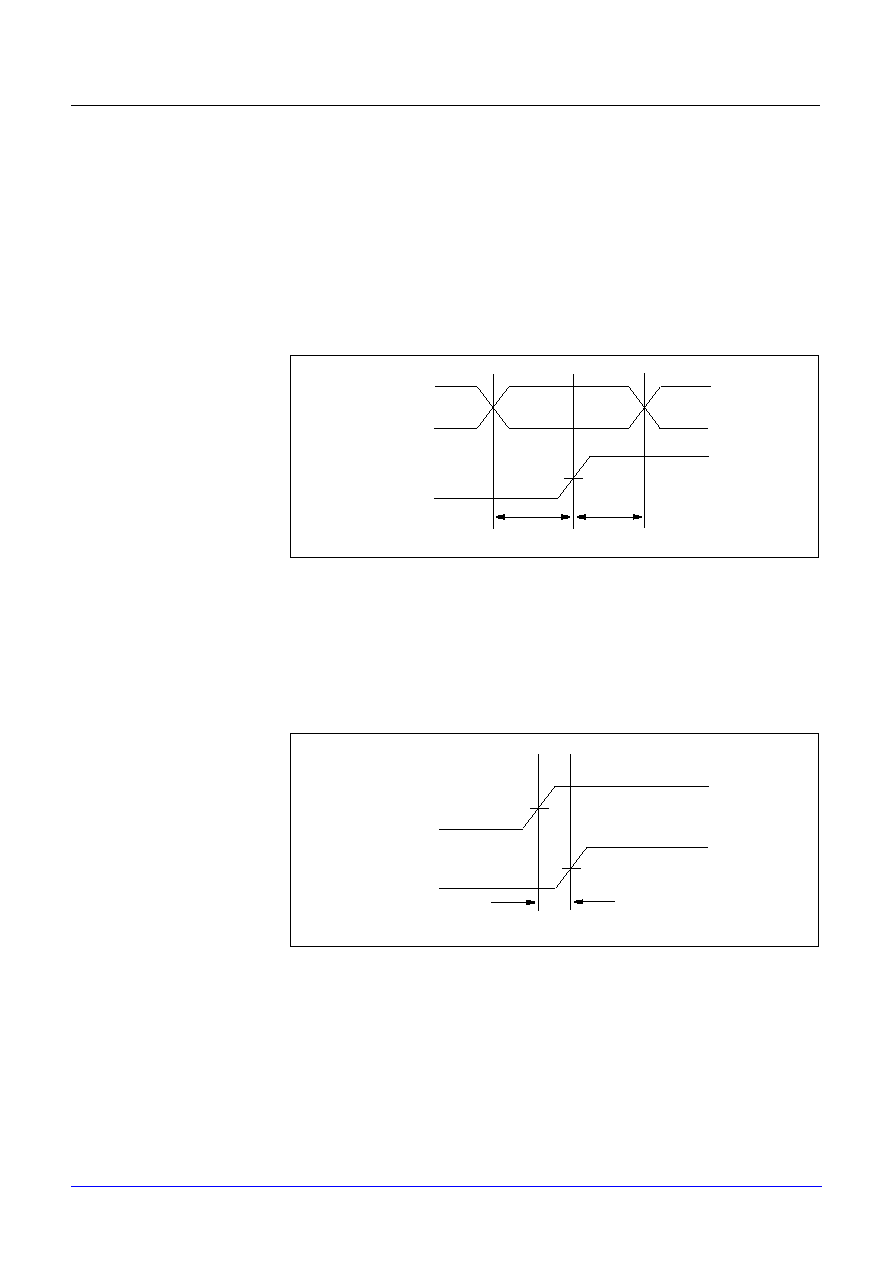
Introduction
1.5 Timings
Samsung ASIC
1-17
STDL130
1.5.2.3 Setup and Hold Time
Setup time, t
SU
, is defined as the minimum time that a signal must be stable
before an active clock transition. Any change to the signal within this time results
in a timing violation, and may result in invalid data being clocked into a
circuit (Figure 1-7).
Hold time, t
HD
, is defined as the minimum time that a signal must remain valid
after an active clock transition. Any change to the signal within this time results in
a timing violation, and may result in invalid data being clocked into a circuit
(Figure 1-7).
Figure 1-7.
Setup and Hold Time
1.5.2.4 Recovery Time
Recovery time, t
RC
, is defined as the time between the release of an
asynchronous control signal from the active state of a circuit to the next active
clock edge (Figure 1-8). If an active clock edge occurs too soon after the release
of the control signal, a violation occurs that may result in erroneous value being
clocked into the circuit.
Figure 1-8.
Recovery Time
D
CK
t
SU
t
HD
50%
50%
50%
RN
CK
t
RC
50%
50%

1.5 Timings
Introduction
STDL130
1-18
Samsung ASIC
1.5.2.5
Removal Time
Removal time, t
RM
, is defined as the minimum time between the active clock edge
and the release of an asynchronous control signal from the active state (Figure 1-
9). If the control signal is released from the active state too soon after an active
clock edge, a violation occurs that may result in erroneous value being clocked
into the circuit.
Figure 1-9.
Removal Time
1.5.2.6
Minimum Pulse Width
Minimum pulse width, t
PW
, is defined as the minimum time allowed for the high or
low phase of a signal and is measured as the time between the rising and falling
edges reaching 50% of the supply voltage (Figure 1-10). A short pulse width
results in a timing violation and may result in the signal not being recognized by
the circuitry.
Figure 1-10.
Minimum Pulse Width
1.5.2.7
Minimum Period
Minimum period, t
PRD
, is defined as the minimum allowable time for one complete
cycle of a signal (Figure 1-11). A short period results in a timing violation and may
result in the signal not being recognized by the circuitry.
Figure 1-11.
Minimum Period
RN
CK
t
RM
50%
50%
CK
t
PWH
50%
t
PWL
CK
50%
t
PRD
Introduction
1.5 Timings
Samsung ASIC
1-19
STDL130
1.5.3 BEST AND WORST CASE CONDITIONS
The timing value of best-case (worst-case) can be calculated by using the
derating factors derived from the following equations:
T
BC
(T
WC
) = K
P
◊
K
T
◊
K
V
◊
T
NOM
where,
T
BC
(T
WC
)
is the best-case (worst-case) timing.
K
P
is the local process derating factor which has different value according to
each cell,
K
T
is the local temperature derating factor which has different value
according to each cell,
K
V
is the local voltage derating factor which has different value according to
each cell,
T
NOM
is the nominal timing characterized under typical-process, 25
∞
C and
1.8V power supply.
The best-case (worst-case) timing values may be determined by picking the
proper derating values from Table 1-3, Table 1-4 and Table 1-5. Derating factors
for conditions between those shown in the tables may be determined by a linear
interpolation.
1.5.4 DERATING FACTORS OF STDL130
Cell timing is primarily determined by cell drive capability and loading determined
by cell input capacitance and wiring. The following critical variables also affect the
timing in a system environment of design:
- Process variation (P)
- Supply voltage (V)
- Junction temperature (T)
Process variation occurs due to the manufacturing environments and the
variation may change the physical characteristics. Its variation affects the
electrical characteristics of devices, increasing or decreasing performance and
power. On the other hand, to design chips which operate in a wide range of
voltage and temperature environments, you have to consider typical-case, worst-
case and best-case conditions to compensate for all variations. To yield much
more timing accuracy, the cell-specific local derating factor is used in STDL130
standard cells.
For an example, the process, temperature and voltage derating factors for an IV
cell are as follows in Table 1-3, Table 1-4 and Table 1-5 respectively.
Table 1-3.
STDL130 Cell Process Derating Factor (K
P
)
Table 1-4.
STDL130 Cell Temperature Derating Factor (K
T
)
Table 1-5.
STDL130 Cell Voltage Derating Factor (K
V
)
Process Factor (K
P
)
Slow
Typ
Fast
1.2226
1.000
0.8952
Temp. (
o
C)
125
85
70
25
0
≠40
K
T
1.0997
1.0611
1.0461
1.000
0.9843
0.9533
Voltage (V)
1.65
1.80
1.95
K
V
1.1295
1.000
0.9338

Introduction
STDL130
1-20
Samsung ASIC
1.5.5
DELAY MODEL
The STDL130 cell timing characteristics consist of the following components:
∑ Cell propagation delay from input to output transitions based on input wave-
form slope, fanout and distributed interconnection wire resistances and
capacitances.
∑ Interconnection wire delay.
∑ Timing requirement parameters including set up time, hold time, recovery
time, skew time, and minimum pulse width.
∑ Derating factors for junction temperature, power supply voltage, and process
variation.
To accomplish accurate timing model, two dimensional table look-up delay model
has been developed. The index variables of this table are input waveform slope
and output load capacitance (Figure 1-12). Samsung's SoC design methodology
supports the n-dimensional table model, even though the two dimensional model
is used.
Figure 1-12.
2-Dimensional Table Delay Model
Table 1-6 shows the propagation delay data for the 2-input NAND cell. The data
in this table is the high-to-low transition delay times from one of the two input
pins to the output pin. The number of points and values of the index variables
can differ for each cell.
Table 1-6.
Table Delay Model Example
\ CAP[pF]
SLOPE[n]
0.005
0.021
0.038
0.073
0.126
0.197
0.019
0.04939
0.09818
0.14943
0.25481
0.41424
0.62777
0.217
0.08564
0.14265
0.19414
0.29981
0.45953
0.67325
0.381
0.10057
0.17403
0.23258
0.33815
0.49775
0.71145
0.708
0.11675
0.21245
0.28991
0.41498
0.57488
0.78819
1.200
0.12799
0.24629
0.34339
0.50214
0.69047
0.90501
Propagation
Delay [ns]
Input Waveform
Slope [ns]
Load
Cap [pF]
1.5
1.0
0.5
1.0
2.0
3.0
0.4
0.8
1.2
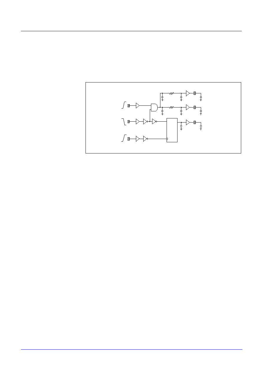
Introduction
Samsung ASIC
1-21
STDL130
Notice that a 5-by-6 table is used. This general table delay model provides great
flexibility as well as high accuracy since extensive software revisions are not
required when a cell library is updated. Other timing components, such as
interconnection wire delay, timing requirement parameters and derating factors
are characterized in a way commonly accepted in the industry. Figure 1-13
summarizes the features of the STDL130 library delay model.
Figure 1-13.
Features of Delay Model
Two dimensional table delay model for output loading and input waveform
slope is used. The rise and fall times and delay times of all cell instances are
calculated recursively.
The input waveform slope of each primary input pad and the loading
capacitance of each primary output pad can be assigned individually or by
default.
Pin to pin delays of cells and interconnection wires are defined.
The effect of distributed interconnection wire resistances and capacitances
on cell delay is analyzed using lumped capacitances.
S1
S3
S2
CO1
CO2
CO3
CK
Q
D
A_Y
B_Y

1.6 Design for Test (DFT) Methodology
Introduction
STDL130
1-22
Samsung ASIC
1.6
Design for Test (DFT)
Methodology
Samsung's libraries are designed with DFT in mind. Samsung's DFT
methodology includes the ability to include full or partial scan path testing,
boundary-scan JTAG for board level testing, Memory BIST, and analog testing.
A brief description of the features of Samsung's scan, BIST, and JTAG as well as
a more detailed discussion of boundary scan architecture follows.
1.6.1 SCAN DESIGN
∑
Multiplexed scan flip-flops that minimize area and delay overhead needed to
implement scan design.
∑
Automated design rule checking, scan insertion, and test pattern generation
∑
High fault coverage on synchronous designs
1.6.2 BIST (BUILT-IN SELF-TEST)
∑
Efficient test solution for compiled memories
∑
At speed and parallel testing of multiple memories
∑
Combination with internal scan design and core testing
1.6.3 BOUNDARY SCAN
∑
IEEE Std 1149.1
∑
JTAG boundary scan registers implemented with primitive cells
∑
Boundary Scan Description Language (BSDL) for board testing
∑
May be combined with internal scan design and core testing
JTAG Boundary Scan Architecture
Boundary scan architecture contains a TAP (Test Access Port), a TAP controller,
an instruction register, and a group of test data registers. The instruction and test
data registers are separated shift-register-based paths connected in parallel with
a common serial data input and a common serial data output. The common serial
data input and output are connected to the TAP, TDI and TDO signals. The TAP
controller selects the alternative instruction and test data register paths between
TDI and TDO. A schematic view of the top level design of the JTAG test logic
archshown in the Figure 1-14.
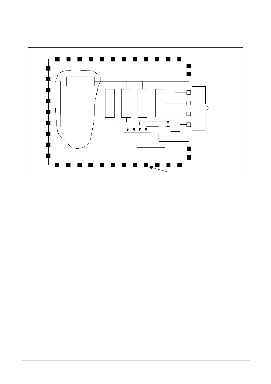
Introduction
1.6 Design for Test (DFT) Methodology
Samsung ASIC
1-23
STDL130
Figure 1-14.
JTAG Boundary Scan Architecure
Functional Block Descriptions
TAP (Test Access Port)
The TAP is a general-purpose port that provides access to many test support functions built into a component
including the test logic. It includes three inputs (TCK -Test Clock Signal; TMS -Test Mode Signal; and TDI -Test
Data Input) and one output (TDO -Test Data Output) required by the test logic. An optional fourth input (TRSTN -
Test Reset) is provided for the asynchronous initialization of the test logic. The values applied at the TMS and TDI
pin are sampled on the rising edge of TCK, and the value placed on TDO changes on the falling edge of TCK.
TAP Controller
The TAP controller receives TCK, interprets the signals on TMS, and generates clock and control signals for both
instruction and test data registers and for other parts of the test circuit as required.
Instruction Register/Instruction Decoder
Test instructions are shifted into and held by the instruction register. Test instructions include tests to be performed
or the test data register addresses to be accessed. A basic 3-bit instruction register and its instruction decoder are
provided as macrofunctions in the library.
Test Data Registers
Test data registers include a bypass register, a boundary scan register, a device identification register and other
design specific registers. Only the bypass and boundary scan registers are mandatory; the rest are optional.
Multiplexer
Scannable
Register
De
vice Identity
Register
Bypass
Register
Instr
uction
Register
TA
P
Controller
SYSTEM
LOGIC
Boundary Scan Path
TDI
TMS
TCK
TDO
TEST
ACCESS
PORT
(TAP)
Mux

1.6 Design for Test (DFT) Methodology
Introduction
STDL130
1-24
Samsung ASIC
The ASIC designer is free to fill in the version and part number in any manner as long as all twenty bits are used.
Samsung's JEDEC code: 78 decimal = 1001110
Continuation field (4 bits) = 0000
Contents of device identification register:
XXXX XXXXXXXXXXXXXXXX 0000 1001110 1
Users can define these two fields.
Test Data Registers Description
Bypass register: The bypass register provides a single-bit serial connection through the circuit when none of
the other test data registers are selected. It can be used to allow test data to flow through a given
device to the other components in a product without affecting a normal operation.
Boundary scan register: The boundary scan register detects typical production defects in board
interconnects, such as opens, and shorts. It also allows access to component inputs and outputs when
testing their logic or sample flow-through signals. Special boundary scan register macrocells are
provided for this purpose.
Design-specific test data register: These optional registers may be provided to allow access to design-
specific test support features in the integrated circuit, such as self-test and scan test.
Device identification register: This is an optional test data register that allows the manufacturer part number
and revision to be identified. The 32-bit identification register is partitioned into four fields:
Device version identifier 1st field
The first four bits beginning from MSB
Device part number
2nd field
16 bits
Manufacturer's JEDEC number
3rd field
11 bits
LSB
4th field
1 bit -- tied in High
Introduction
1.7 Maximum Fanouts
Samsung ASIC
1-25
STDL130
1.7
Maximum Fanouts
1.7.1 PRIMITIVE CELLS
The maximum fanout for STDL130
primitive cells is tabulated in Table 1-
7 and Appendix C. Note that these
fanout limitation values are calcu-
lated when the rise and fall time of
the input signal are 0.217ns.
Depending on the rise and fall time,
the maximum fanout limitations can
be varied case by case.
In the following table the maximum
fanout values for all pins of STDL130
primitive cells are listed.
Table 1-7.
Maximum Fanouts
of Primitive Cells
(When input t
R
/t
F
= 0.217ns,
one fanout (SL) = 0.00515pF)
Cell Name
Output
Pin
Maximum
Fanout
ad2_lp
Y
38
ad2b_lp
Y
38
ad2bd2_lp
Y
78
ad2bd4_lp
Y
156
ad2bd8_lp
Y
311
ad2d2_lp
Y
77
ad2d4_lp
Y
155
ad2d8_lp
Y
310
ad3_lp
Y
39
ad3d2_lp
Y
77
ad3d4_lp
Y
152
ad4_lp
Y
39
ad4d2_lp
Y
77
ad4d4_lp
Y
151
ad5_lp
Y
18
ad5d2_lp
Y
36
ad5d4_lp
Y
158
ao21_lp
Y
17
ao211_lp
Y
10
ao2111_lp
Y
6
ao2111d2_lp
Y
78
ao211d2_lp
Y
21
ao211d4_lp
Y
158
ao21d2_lp
Y
34
ao21d4_lp
Y
157
ao22_lp
Y
17
ao221_lp
Y
9
ao221d2_lp
Y
77
ao221d4_lp
Y
157
ao222_lp
Y
9
ao2222_lp
Y
6
ao2222d2_lp
Y
77
ao2222d4_lp
Y
158
ao222a_lp
Y
14
ao222d2_lp
Y
78
ao222d4_lp
Y
158
ao22a_lp
Y
16
ao22d2_lp
Y
33
ao22d4_lp
Y
156
ao31_lp
Y
16
ao311_lp
Y
9
ao3111_lp
Y
5
ao31d2_lp
Y
33
ao31d4_lp
Y
156
ao32_lp
Y
16
ao321_lp
Y
8
ao322_lp
Y
8
ao32d2_lp
Y
78
ao33_lp
Y
15
ao331_lp
Y
8
ao332_lp
Y
8
busholder_lp
Y
10000
cglp_lp
GCK
37
cglpd2_lp
GCK
76
cglpd4_lp
GCK
154
cglp
GCK
38
cglpd2
GCK
78
cglpd4
GCK
156
dl1d2
Y
77
dl2d2
Y
77
dl5d2
Y
78
dl10d2
Y
78
fa_lp
S
39
CO
38
fad2_lp
S
78
CO
78
fd1_lp
Q
38
QN
38
fd1d2_lp
Q
77
QN
77
fd1q_lp
Q
38
fd1qd2_lp
Q
78
fd1s_lp
Q
38
QN
38
fd1sd2_lp
Q
78
QN
78
fd1sq_lp
Q
38
fd1sqd2_lp
Q
78
fd2_lp
Q
38
QN
38
fd2d2_lp
Q
78
QN
78
fd2q_lp
Q
39
fd2qd2_lp
Q
79
fd2s_lp
Q
39
QN
38
fd2sd2_lp
Q
78
QN
78
fd2sq_lp
Q
39
fd2sqd2_lp
Q
79
fd3_lp
Q
38
QN
38
fd3d2_lp
Q
77
QN
77
fd3q_lp
Q
38
fd3qd2_lp
Q
78
fd3s_lp
Q
38
QN
39
fd3sd2_lp
Q
78
QN
79
fd3sq_lp
Q
38
fd3sqd2_lp
Q
78
fd4_lp
Q
39
QN
38
fd4d2_lp
Q
78
QN
77
fd4q_lp
Q
39
fd4qd2_lp
Q
78
Cell Name
Output
Pin
Maximum
Fanout
1.7 Maximum Fanouts
Introduction
STDL130
1-26
Samsung ASIC
fd4s_lp
Q
39
QN
38
fd4sd2_lp
Q
79
QN
77
fd4sq_lp
Q
39
fd4sqd2_lp
Q
79
fd5_lp
Q
38
QN
38
fd5d2_lp
Q
77
QN
77
fd5s_lp
Q
38
QN
38
fd5sd2_lp
Q
78
QN
78
fd6_lp
Q
39
QN
38
fd6d2_lp
Q
78
QN
78
fd6s_lp
Q
39
QN
38
fd6sd2_lp
Q
78
QN
78
fd7_lp
Q
38
QN
39
fd7d2_lp
Q
78
QN
79
fd7s_lp
Q
38
QN
39
fd7sd2_lp
Q
78
QN
79
fd8_lp
Q
39
QN
38
fd8d2_lp
Q
79
QN
77
fd8s_lp
Q
39
QN
38
fd8sd2_lp
Q
78
QN
77
fds2_lp
Q
38
QN
38
fds2d2_lp
Q
78
QN
78
fds2s_lp
Q
38
QN
38
fds2sd2_lp
Q
78
QN
78
fds3_lp
Q
38
QN
38
fds3d2_lp
Q
78
QN
78
fds3s_lp
Q
38
QN
38
fds3sd2_lp
Q
78
QN
78
fj2_lp
Q
39
QN
38
fj2d2_lp
Q
79
QN
78
fj2s_lp
Q
39
QN
38
fj2sd2_lp
Q
79
QN
78
fj4_lp
Q
38
QN
39
fj4d2_lp
Q
77
QN
78
Cell Name
Output
Pin
Maximum
Fanout
fj4s_lp
Q
39
QN
38
fj4sd2_lp
Q
78
QN
77
ft2_lp
Q
39
QN
38
ft2d2_lp
Q
79
QN
78
ha_lp
S
38
CO
38
had2_lp
S
78
CO
77
iv_lp
Y
39
ivd2_lp
Y
81
ivd3_lp
Y
121
ivd4_lp
Y
160
ivd6_lp
Y
242
ivd8_lp
Y
323
ivd16_lp
Y
648
ivd24_lp
Y
968
ivt_lp
Y
38
ivtd2_lp
Y
78
ivtd4_lp
Y
157
ivtd8_lp
Y
311
ivtd16_lp
Y
615
ld1_lp
Q
39
QN
38
ld1d2_lp
Q
77
QN
77
ld1q_lp
Q
39
ld1qd2_lp
Q
79
ld2_lp
Q
38
QN
38
ld2d2_lp
Q
77
QN
78
ld2q_lp
Q
39
ld2qd2_lp
Q
78
ld3_lp
Q
38
QN
38
ld3d2_lp
Q
78
QN
78
ld4_lp
Q
38
QN
39
ld4d2_lp
Q
78
QN
78
ld5_lp
Q
38
QN
38
ld5d2_lp
Q
78
QN
79
ld5q_lp
Q
39
ld5qd2_lp
Q
77
ld6_lp
Q
38
QN
38
ld6d2_lp
Q
77
QN
79
ld6q_lp
Q
39
ld6qd2_lp
Q
78
mx2_lp
Y
39
mx2d2_lp
Y
78
mx2d4_lp
Y
158
mx2i_lp
YN
17
mx2ia_lp
YN
17
mx2id2_lp
YN
34
mx2id2a_lp
YN
34
mx2id4_lp
YN
155
mx2id4a_lp
YN
156
Cell Name
Output
Pin
Maximum
Fanout
Introduction
1.7 Maximum Fanouts
Samsung ASIC
1-27
STDL130
mx4_lp
Y
38
mx4d2_lp
Y
77
mx4d4_lp
Y
150
nd2_lp
Y
38
nd2b_lp
Y
38
nd2bd2_lp
Y
77
nd2bd4_lp
Y
153
nd2bd8_lp
Y
312
nd2d2_lp
Y
77
nd2d4_lp
Y
154
nd2d8_lp
Y
309
nd3_lp
Y
26
nd3b_lp
Y
26
nd3bd2_lp
Y
54
nd3bd4_lp
Y
154
nd3bd8_lp
Y
311
nd3d2_lp
Y
54
nd3d4_lp
Y
154
nd3d8_lp
Y
311
nd4_lp
Y
20
nd4d2_lp
Y
40
nd4d4_lp
Y
154
nd5_lp
Y
38
nd5d2_lp
Y
77
nd5d4_lp
Y
156
nd6_lp
Y
38
nd6d2_lp
Y
77
nd6d4_lp
Y
156
nd8_lp
Y
38
nd8d2_lp
Y
76
nd8d4_lp
Y
156
nid_lp
Y
38
nid16_lp
Y
619
nid2_lp
Y
78
nid3_lp
Y
116
nid4_lp
Y
156
nid6_lp
Y
234
nid8_lp
Y
311
nid24_lp
Y
936
nit_lp
Y
38
nitd16_lp
Y
612
nitd2_lp
Y
78
nitd4_lp
Y
157
nitd8_lp
Y
311
nr2_lp
Y
18
nr2a_lp
Y
37
nr2b_lp
Y
18
nr2bd2_lp
Y
36
nr2bd4_lp
Y
156
nr2bd8_lp
Y
312
nr2d2_lp
Y
36
nr2d4_lp
Y
156
nr2d8_lp
Y
312
nr3_lp
Y
11
nr3a_lp
Y
23
nr3d2_lp
Y
23
nr3d4_lp
Y
156
nr4_lp
Y
38
nr4d2_lp
Y
78
nr4d4_lp
Y
158
nr5_lp
Y
38
nr5d2_lp
Y
77
nr5d4_lp
Y
156
nr6_lp
Y
38
nr6d2_lp
Y
77
nr6d4_lp
Y
158
Cell Name
Output
Pin
Maximum
Fanout
nr8_lp
Y
38
nr8d2_lp
Y
77
nr8d4_lp
Y
154
oa21_lp
Y
17
oa211_lp
Y
16
oa2111_lp
Y
17
oa2111d2_lp
Y
33
oa211d2_lp
Y
34
oa211d4_lp
Y
156
oa21d2_lp
Y
35
oa21d4_lp
Y
156
oa22_lp
Y
16
oa221_lp
Y
15
oa221d2_lp
Y
32
oa221d4_lp
Y
156
oa222_lp
Y
14
oa2222_lp
Y
11
oa2222d2_lp
Y
78
oa2222d4_lp
Y
158
oa222d2_lp
Y
30
oa222d4_lp
Y
158
oa22a_lp
Y
17
oa22d2_lp
Y
33
oa22d2a_lp
Y
35
oa22d4_lp
Y
157
oa22d4a_lp
Y
156
oa31_lp
Y
11
oa311_lp
Y
10
oa3111_lp
Y
9
oa31d2_lp
Y
22
oa31d4_lp
Y
156
oa32_lp
Y
9
oa321_lp
Y
9
oa322_lp
Y
8
oa33_lp
Y
9
or2_lp
Y
38
or2b_lp
Y
38
or2bd2_lp
Y
77
or2bd4_lp
Y
155
or2bd8_lp
Y
312
or2d2_lp
Y
77
or2d4_lp
Y
155
or2d8_lp
Y
310
or3_lp
Y
38
or3d2_lp
Y
78
or3d4_lp
Y
156
or4_lp
Y
37
or4d2_lp
Y
75
or4d4_lp
Y
155
or5_lp
Y
38
or5d2_lp
Y
76
or5d4_lp
Y
156
scg1_lp
Y
26
scg1d2_lp
Y
53
scg2_lp
Y
38
scg2d2_lp
Y
77
scg2d4_lp
Y
155
scg3_lp
Y
26
scg3d2_lp
Y
53
scg3d4_lp
Y
155
scg4_lp
Y
38
scg4d2_lp
Y
77
scg4d4_lp
Y
152
scg5_lp
Y
37
scg5d2_lp
Y
76
scg5d4_lp
Y
153
Cell Name
Output
Pin
Maximum
Fanout
1.7 Maximum Fanouts
Introduction
STDL130
1-28
Samsung ASIC
scg6_lp
Y
38
scg6d2_lp
Y
78
scg7_lp
Y
38
scg7d2_lp
Y
75
scg8_lp
Y
38
scg8d2_lp
Y
78
scg9_lp
Y
38
scg9d2_lp
Y
79
scg10_lp
Y
38
scg10d2_lp
Y
78
scg11_lp
Y
11
scg11d2_lp
Y
23
scg12_lp
Y
18
scg12d2_lp
Y
36
scg12d4_lp
Y
156
scg13_lp
Y
38
scg13d2_lp
Y
77
scg14_lp
Y
37
scg14d2_lp
Y
76
scg15_lp
Y
26
scg15d2_lp
Y
53
scg16_lp
Y
17
scg16d2_lp
Y
35
scg17_lp
Y
37
scg17d2_lp
Y
77
scg18_lp
Y
26
scg18d2_lp
Y
54
scg19_lp
Y
17
scg19d2_lp
Y
34
scg20_lp
Y
18
scg20d2_lp
Y
36
scg21_lp
Y
11
scg21d2_lp
Y
23
scg22_lp
Y
17
scg22d2_lp
Y
35
xn2_lp
Y
39
xn2d2_lp
Y
78
xn2d4_lp
Y
154
xn3_lp
Y
38
xn3d2_lp
Y
75
xn3d4_lp
Y
146
xo2_lp
Y
39
xo2d2_lp
Y
78
xo2d4_lp
Y
155
xo3_lp
Y
37
xo3d2_lp
Y
75
xo3d4_lp
Y
151
Cell Name
Output
Pin
Maximum
Fanout
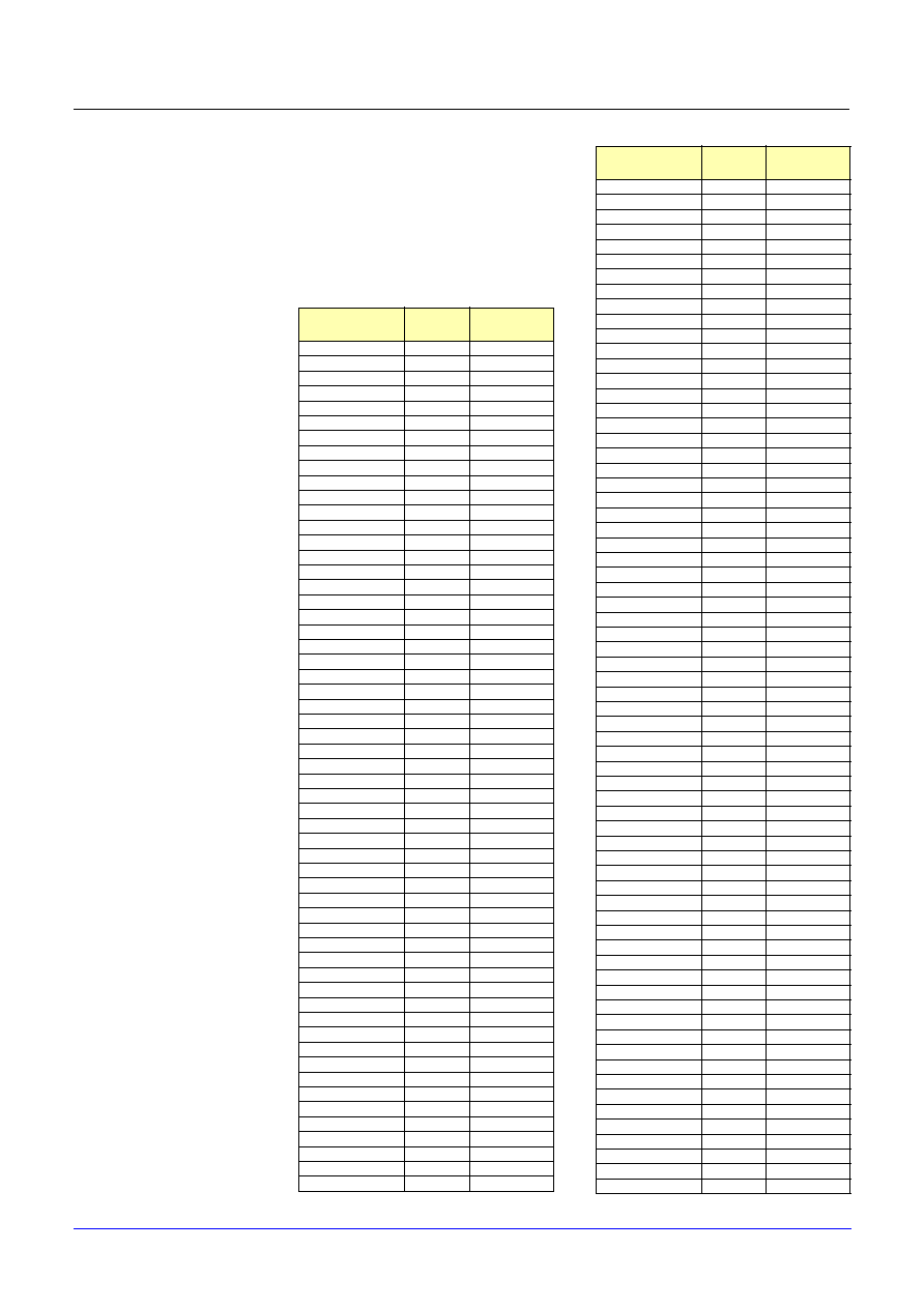
Introduction
1.7 Maximum Fanouts
Samsung ASIC
1-29
STDL130
1.7.2 I/O Cells
The maximum fanout for I/O cells are
listed as follows.
Table 1-8.
Maximum Fanouts
of I/O Cells
(When input t
R
/t
F
= 0.217ns,
one fanout (SL) = 0.00515pF)
Cell Name
Output
Pin
Maximum
Fanout
phic_lp
Y
166
phic_abb_lp
Y
222
phicc_abb_lp
Y
225
phicd_lp
Y
166
phicd_abb_lp
Y
222
phicen_abb_lp
Y
219
phicu_lp
Y
166
phicu_abb_lp
Y
222
phis_lp
Y
166
phis_abb_lp
Y
217
phisd_lp
Y
166
phisd_abb_lp
Y
217
phisu_lp
Y
166
phisu_abb_lp
Y
217
phsckdc2_lp
Y
552
phsckdc4_lp
Y
1074
phsckdc6_lp
Y
1542
phsckdc8_lp
Y
1946
phsckdcd2_lp
Y
552
phsckdcd4_lp
Y
1074
phsckdcd6_lp
Y
1542
phsckdcd8_lp
Y
1946
phsckdcu2_lp
Y
552
phsckdcu4_lp
Y
1074
phsckdcu6_lp
Y
1542
phsckdcu8_lp
Y
1946
phsckds2_lp
Y
552
phsckds4_lp
Y
1074
phsckds6_lp
Y
1542
phsckds8_lp
Y
1946
phsckdsd2_lp
Y
552
phsckdsd4_lp
Y
1074
phsckdsd6_lp
Y
1542
phsckdsd8_lp
Y
1946
phsckdsu2_lp
Y
552
phsckdsu4_lp
Y
1074
phsckdsu6_lp
Y
1542
phsckdsu8_lp
Y
1946
phtic_lp
Y
166
phticd_lp
Y
166
phticu_lp
Y
166
phtis_lp
Y
166
phtisd_lp
Y
166
phtisu_lp
Y
166
phsosck1_lp
YN
135
phsosck17_lp
YN
135
phsosck2_lp
YN
42
phsosck27_lp
YN
42
phsoscm1_lp
YN
51
phsoscm16_lp
YN
51
phsoscm2_lp
YN
429
phsoscm26_lp
YN
430
phsoscm3_lp
YN
516
phsoscm36_lp
YN
524
pic_lp
Y
253
pic_abb_lp
Y
253
picc_abb_lp
Y
257
picd_lp
Y
253
picd_abb_lp
Y
253
picen_abb_lp
Y
244
picu_lp
Y
252
picu_abb_lp
Y
252
pis_lp
Y
248
pis_abb_lp
Y
248
pisd_lp
Y
248
pisd_abb_lp
Y
248
pisu_lp
Y
248
pisu_abb_lp
Y
248
pmic_lp
Y
106
pmic_abb_lp
Y
171
pmicc_abb_lp
Y
172
pmicd_lp
Y
106
pmicd_abb_lp
Y
170
pmicen_abb_lp
Y
165
pmicu_lp
Y
106
pmicu_abb_lp
Y
168
pmis_lp
Y
106
pmis_abb_lp
Y
168
pmisd_lp
Y
106
pmisd_abb_lp
Y
168
pmisu_lp
Y
106
pmisu_abb_lp
Y
168
pmsckdc2_lp
Y
553
pmsckdc4_lp
Y
1075
pmsckdc6_lp
Y
1545
pmsckdc8_lp
Y
1951
pmsckdcd2_lp
Y
553
pmsckdcd4_lp
Y
1075
pmsckdcd6_lp
Y
1545
pmsckdcd8_lp
Y
1951
pmsckdcu2_lp
Y
553
pmsckdcu4_lp
Y
1075
pmsckdcu6_lp
Y
1545
pmsckdcu8_lp
Y
1951
pmsckds2_lp
Y
553
pmsckds4_lp
Y
1075
pmsckds6_lp
Y
1545
pmsckds8_lp
Y
1951
pmsckdsd2_lp
Y
553
pmsckdsd4_lp
Y
1075
pmsckdsd6_lp
Y
1545
pmsckdsd8_lp
Y
1951
pmsckdsu2_lp
Y
553
pmsckdsu4_lp
Y
1075
pmsckdsu6_lp
Y
1545
pmsckdsu8_lp
Y
1951
pmsosck1_lp
YN
136
pmsosck2_lp
YN
42
pmsoscm1_lp
YN
50
pmsoscm2_lp
YN
206
psckdc2_lp
Y
608
psckdc4_lp
Y
1183
psckdc6_lp
Y
1709
psckdc8_lp
Y
2171
psckdcd2_lp
Y
608
psckdcd4_lp
Y
1184
psckdcd6_lp
Y
1708
psckdcd8_lp
Y
2166
psckdcu2_lp
Y
608
psckdcu4_lp
Y
1182
psckdcu6_lp
Y
1708
psckdcu8_lp
Y
2170
psckds2_lp
Y
603
psckds4_lp
Y
1148
psckds6_lp
Y
1606
Cell Name
Output
Pin
Maximum
Fanout
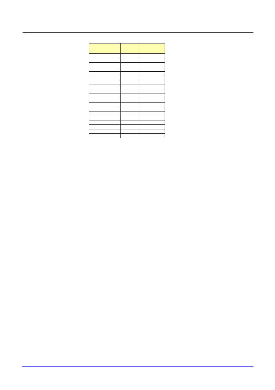
1.7 Maximum Fanouts
Introduction
STDL130
1-30
Samsung ASIC
psckds8_lp
Y
1971
psckdsd2_lp
Y
603
psckdsd4_lp
Y
1146
psckdsd6_lp
Y
1601
psckdsd8_lp
Y
1962
psckdsu2_lp
Y
603
psckdsu4_lp
Y
1147
psckdsu6_lp
Y
1605
psckdsu8_lp
Y
1967
psosck1_lp
YN
227
psosck2_lp
YN
231
psoscm1_lp
YN
232
psoscm2_lp
YN
232
ptic_lp
Y
250
pticd_lp
Y
249
pticu_lp
Y
250
ptis_lp
Y
244
ptisd_lp
Y
208
ptisu_lp
Y
244
Cell Name
Output
Pin
Maximum
Fanout

Introduction
Samsung ASIC
1-31
STDL130
<Condition>
∑
Library = STDL130
∑
V
DD
= 1.8V
∑
Fanout = 0.00466pF (= input capacitance for CK pin of FD1_LP)
∑
Standard Load (SL) = 0.00515pF
∑
Input slope = 0.217ns
∑
Maximum output transition time (MOTT) = 1.2ns
∑
Maximum frequency
300MHz
∑
Net length (
µ
m/fanout): branch net length for each fanout except trunk
For high fanout nets including clock net, Samsung strongly recommends using
clock tree synthesis.
Trunk width (
µ
m)
8
In case that
interconnection
is not considered
Net length
(
µ
m/fanout)
20
200
Trunk length (
µ
m)
2000
5000
2000
5000
ck2_lp
259
163
60
37
662
ck4_lp
561
434
129
100
1321
ck6_lp
851
674
196
155
1984
ck8_lp
1125
881
259
203
2643
Trunk width (
µ
m)
0.28
8
In case that
interconnection
is not considered
Net length
(
µ
m/fanout)
20
200
Trunk length (
µ
m)
2000
5000
2000
5000
nid_lp
-
-
-
-
38
nid2_lp
17
-
-
-
78
nid3_lp
32
-
-
-
116
nid4_lp
48
-
6
-
156
nid6_lp
74
11
17
-
234
nid8_lp
94
19
27
4
311
nid16_lp
147
33
68
43
619
nid24_lp
173
38
109
80
936

1.8 Package Capability by Pitch and Lead Count
Introduction
STDL130
1-32
Samsung ASIC
1.8
PACKAGE
CAPABILITY BY PITCH
AND LEAD COUNT
See Appendix D for Samsung's package capability as of this writing. The most
current package availability and capability can be obtained from your local
Samsung Technology and Design Centers.

Introduction
1.9 Power Dissipation
Samsung ASIC
1-33
STDL130
1.9
Power
Dissipation
1.9.1 ESTIMATION OF POWER DISSIPATION IN CMOS CIRCUIT
A primary advantage of CMOS circuits is low power consumption since they draw
a very small amount of current under steady state, DC conditions. However, as
circuit densities and clock rates increase, the power dissipation in CMOS circuits
becomes substantial. Power dissipation in CMOS circuits is affected by various
factors such as the number of gates, the switching frequency, and output loads
of gates.
Circuit operating temperature is an important factor in determining circuit speed
and reliability. Circuit power dissipation is a major factor in determining circuit
operating temperature. Designers must estimate the power dissipation of a circuit
accurately and choose the appropriate package and system operating conditions
for the circuit to insure the best performance and reliability.
The following sections describe the components of power dissipation in a CMOS
circuit (static and dynamic), and the method of calculating them for the Samsung
STDL130 library elements.
1.9.2 STATIC (DC) POWER DISSIPATION
Two types of static or DC current contribute to the total static power dissipation in
CMOS circuits - leakage current and input/output current.
Leakage current results from a reverse bias between the well and the substrate
region of the CMOS circuit. Since there is no DC current path from power to
ground through a CMOS logic gate in steady state, no static current except
leakage current flows through the internal circuitry of a CMOS device. The
amount of this leakage current is normally on the order of tens of nano amperes
and is negligible.
Input/output current flows through I/O buffers when the circuit is interfaced with
other devices, especially TTL. The current of pull-up/pull-down transistor in the
input buffers is typically on the order of tens of micro amperes (33
µ
A at 3.3V,
25
µ
A at 2.5V, and 18
µ
A at 1.8V), which is also negligible. Therefore, only the DC
current that the output buffers source or sink needs to be counted to estimate total
static power dissipation. The DC power dissipation of output and bi-directional
buffers is determined by the following formula:
where,
n = Number of output and bidirectional buffers
T = Total operation time in output mode
t
H
= The sum of logic high state time
t
L
= The sum of logic low state time
t
L
+ t
H
= T (assuming that output and bi-directional buffers are not tri-state)
S
out
is the output mode ratio of bi-directional buffers (typically 0.5)
P
DC_OUTPUT
[mW]
V
OL k
( )
I
OL k
( )
t
L k
( )
◊
◊
(
)
k 1
=
n
V
DD
V
OH k
( )
≠
(
)
I
OH k
( )
t
H k
( )
◊
◊
(
)
k 1
=
n
+
T
/
=
P
DC_BI
[mW]
V
OL k
( )
I
OL k
( )
t
L k
( )
◊
◊
(
)
k 1
=
n
V
DD
V
OH k
( )
≠
(
)
I
OH k
( )
t
H k
( )
◊
◊
(
)
k 1
=
n
+
S
out
T
/
◊
=

1.9 Power Dissipation
Introduction
STDL130
1-34
Samsung ASIC
1.9.3 DYNAMIC (AC) POWER DISSIPATION
When a CMOS logic gate changes state, it draws switching current as a result of charging or discharging a load
capacitance, C
L
. The power associated with the switching current for a node capacitance, C
L
, is
where V
DD
is the power supply voltage.
In addition to the power dissipated by changing the load capacitance, CMOS circuits consume power due to
current flowing from the power supply to ground through the n- and p-channel transistors during switching.
The dynamic power dissipation for an entire chip is difficult to estimate since it depends on the switching activity
of the circuit. Samsung has found that switching activity is about 10% on the average and recommends using this
number in estimating total dynamic power dissipation.
1.9.4 POWER DISSIPATION IN STDL130
This section describes the equations used to estimate the power dissipation in STDL130. As explained in the
previous section, the total power dissipation (P
TOTAL
) consists of static power dissipation (P
DC
) and dynamic
power dissipation (P
AC
). Samsung's internal power estimation tool, CubicPower, uses a methodology based on
the following equations.
P
TOTAL
= P
AC
+ P
DC
P
DC
is negligible in case of CMOS logic in general.
The dynamic power dissipation is caused by four components: input buffers (P
AC_INPUT
), output buffers
(P
AC_OUTPUT
), bi-directional buffers (P
AC_BI
), and internal cells (P
AC_INTERNAL
).
P
AC
= P
AC_ INPUT
+ P
AC_OUTPUT
+ P
AC_BI
+ P
AC_INTERNAL
C
L
V
DD
◊
2

Introduction
1.9 Power Dissipation
Samsung ASIC
1-35
STDL130
Each term mentioned above is characterized by the following equations:
where,
N_1.8V_input is the number of 1.8V interface input buffers used,
N_2.5V_input is the number of 2.5V interface input buffers used,
N_3.3V_input is the number of 3.3V interface input buffers used,
N_total_input = N_1.8V_input + N_2.5V_input + N_3.3V_input,
N_1.8V_output is the number of 1.8V interface output buffers used,
N_2.5V_output is the number of 2.5V interface output buffers used,
N_3.3V_output is the number of 3.3V interface output buffers used,
N_1.8V_bi is the number of 1.8V interface bi-directional buffers used,
N_2.5V_bi is the number of 2.5V interface bi-directional buffers used,
N_3.3V_bi is the number of 3.3V interface bi-directional buffers used,
N_total_bi = N_1.8V_bi + N_2.5V_bi + N_3.3V_bi,
N_macro is the number of macro cells used,
G is total gate count of the design,
F is the operating frequency in MHz,
S is the estimated switching activity (typically 0.1 for internal logic and 0.5 for I/O),
S
out
is the output mode ratio of bi-directional buffers (typically 0.5),
C is the load capacitance in pF,
P is the characterized power for the i-th hard macro block (
µ
W/MHz)
P
AC_INPUT
[mW]
1.8
I
i_eq_p
F
i
100
---------- S
i
◊
◊
2.5
+
i
N_1.8V_input
◊
I
j_eq_p
F
j
100
---------- S
j
◊
◊
j
N_2.5V_input
◊
3.3
+
I
k_eq_p
F
k
100
---------- S
k
◊
◊
3.24
+
k
N_3.3V_input
◊
0.001 S
l
◊
F
l
◊
C
l_inload
◊
(
)
l
N_total_input
◊
=
P
AC_OUTPUT
[mW]
1.8
I
i_eq_p
F
i
100
---------- S
i
◊
◊
2.5
+
i
N_1.8V_output
◊
I
j_eq_p
F
j
100
---------- S
j
◊
◊
+
j
N_2.5V_output
◊
=
3.3
I
k_eq_p
F
k
100
---------- S
k
◊
◊
k
N_3.3V_output
◊
3.24
0.001 S
i
F
i
C
i_outload
◊
◊
◊
(
)
i
N_1.8V_output
◊
+
+
6.25
0.001 S
j
F
j
C
j_outload
◊
◊
◊
(
)
j
N_2.5V_output
◊
10.89
+
0.001 S
k
F
k
C
k_outload
◊
◊
◊
(
)
k
N_3.3V_output
◊
P
AC_BI
[mW]
P
AC_BI_INPUT
◊
1 S
out
≠
(
)
P
AC_BI_OUTPUT
S
out
◊
+
=
P
AC_BI_INPUT
[mW]
1.8
I
i_eq_p
F
i
100
---------- S
i
◊
◊
i
N_1.8V_bi
◊
2.5
+
I
j_eq_p
F
j
100
---------- S
j
◊
◊
j
N_2.5V_bi
3.3
I
k_eq_p
F
k
100
---------- S
k
◊
◊
3.24
+
k
N_3.3V_bi
0.001 S
l
F
l
C
l_inload
◊
◊
◊
(
)
l
N_total_bi
◊
◊
+
◊
=
P
AC_BI_OUTPUT
[mW]
1.8
I
i_eq_p
F
i
100
---------- S
i
◊
◊
2.5
+
i
N_1.8V_bi
◊
I
j_eq_p
F
j
100
---------- S
j
◊
◊
+
j
N_2.5V_bi
◊
=
3.3
I
k_eq_p
F
k
100
---------- S
k
◊
◊
k
N_3.3V_bi
◊
3.24
0.001 S
i
F
i
C
i_outload
◊
◊
◊
(
)
i
N_1.8V_bi
◊
+
+
6.25
0.001 S
j
F
j
C
j_outload
◊
◊
◊
(
)
j
N_2.5V_bi
◊
10.89
+
0.001 S
k
F
k
C
k_outload
◊
◊
◊
(
)
k
N_3.3V_bi
◊
P
AC_INTERNAL
[mW]
0.001
0.0705 S 0.0076
+
◊
(
)
◊
G F
0.001 P
i
◊
F
i
◊
(
)
i
N_macro
+
◊
◊
=
1.9 Power Dissipation
Introduction
STDL130
1-36
Samsung ASIC
1.9.5 TEMPERATURE AND POWER DISSIPATION
The total power dissipation, P
TOTAL
can be used to find out the device temperature by the following equation:
T
J
=
JA
◊
P
TOTAL
+ T
A
where,
JA
is the package thermal impedance,
T
J
is the junction temperature of the device,
T
A
is the ambient temperature.
Thermal impedances of the Samsung packages are given in the following table. The junction temperature
determines the derating factor for the propagation delays and is also used in reliability calculations. Hence,
designers can achieve the desired derating factor and reliability targets by choosing appropriate packages and
system cooling methods.
Table 1-11.
Thermal Impedances of Samsung Plastic Packages
SOP/TSOP
Pin Number
20
24
28
32
44
50
54
62
66
JA
[
∞
C/W]
63
58
41-44
46-56
44-71
39-59
34-56
27-33
34-46
QFP
Pin Number
44
48
80
100
120
128
160
208
240
256
JA
[
∞
C/W]
51-62
43-56
43-74
27-61
33-47
43-51
29-51
22-43
28-47
29-42
TQFP/LQFP
Pin Number
32
64
100
144
160
176
208
256
JA
[
∞
C/W]
68-70
47
37-70
38
35-62
31-34
37-56
30-42
PBGA
Pin Number
272
388
356 (TEPBGA)
452 (TEPBGA)
JA
[
∞
C/W]
19-22
16-19
16
14
SBGA
Pin Number
256
304
352
432
600
JA
[
∞
C/W]
14.1
13.1
11.7
10.2
8.3

Introduction
1.10 VDD/VSS Rules And Guidelines
Samsung ASIC
1-37
STDL130
1.10
V
DD
/V
SS
Rules
And Guidelines
Three kinds of power supplies exist in STDL130 providing power to internal and
I/O areas:
∑
Core logic
≠ VDD1IH_LP, VDD1IM_LP, VDD1I_LP, VSS3I_LP, VSS2I_LP, VSS1I_LP
∑
Pre-driver (I/O area)
≠ VDD3P_LP, VDD2P_LP, VDD1P_LP, VSS3P_LP, VSS2P_LP, VSS1P_LP
∑
Output-driver (I/O area)
≠ VDD3O_LP, VDD2O_LP, VDD1O_LP, VSS3O_LP, VSS2O_LP, VSS1O_LP
The number of V
DD
and V
SS
pads required for a specific design depends on the
following factors:
∑
Number of input and output buffers
∑
Number of simultaneous switching outputs
∑
Number of used gates and simultaneous switching gates
∑
Operating frequency
1.10.1 BASIC PLACEMENT GUIDELINES
The purpose of these guidelines is to minimize IR drop and noise for reliable
device operations.
∑
Core logic and pre-driver V
DD
/V
SS
pads should be evenly distributed on all
sides of the chip.
∑
If you have core block demanding high power (compiled memory, analog),
extra power pads should be used to supply that block.
∑
Power pads for SSO group should be evenly distributed in the SSO group.
∑
Do not place the quiet signal (analog, reference), analog power (VDDA/
VSSA), or bi-directional buffer next to the SSO group.
∑
Opposite types of power pads (V
DD
/V
SS
) should be placed as close together
as possible.
∑
If possible, do not place power pads (V
DD
/V
SS
) at the corner of the chip.
1.10.2 VDD1I_LP/VSS1I_LP ALLOCATION GUIDELINES
The purpose of these guidelines is to ensure that the minimum number of core
logic power pad pairs are used while meeting the electromigration rules. The
number of VDD1I_LP/VSS1I_LP pads required for a specific design is a function
of the operating frequency of a chip.
∑
VDD1I_LP bus width and the number of pads are equal to those of
VSS1I_LP
∑
VDD1I_LP/VSS1I_LP buses and pads should be distributed evenly in the
core and on each side of the chip.
1.10 VDD/VSS Rules And Guidelines
Introduction
STDL130
1-38
Samsung ASIC
The number of VDD1I_LP/VSS1I_LP pad pairs required for a design can be calculated from the following
expression:
The number of VDD1I_LP/VSS1I_LP pad pairs =
where,
G = The core (excluding hard macro blocks) size in the gate counts
S = The switching ratio (typically = 0.1)
F = Operating frequency (MHz)
Pi = Characterized current for the i-th hard macro block (mA/MHz)
Fi = Operating frequency for the i-th hard macro block (MHz)
I
em
= Current limit per V
DD
/V
SS
pad pairs based on electromigration rule (40mA)
For reliable device operation and to minimum IR drop, no device should have fewer than 4 VDD1I_LP/VSS1I_LP
power pad pairs.
Extra power pad pairs may be needed for high power consuming macro blocks (SRAM, analog blocks, etc.).
1.10.3 VDD1P_LP/VSS1P_LP (VDD2P_LP, 3P_LP/VSS2P_LP, 3P_LP) ALLOCATION GUIDELINES.
These guidelines ensure that adequate input threshold voltage margin is maintained during I/O switching.
The number of VDD1P_LP/VSS1P_LP, VDD2P_LP/VSS2P_LP, VDD3P_LP/VSS3P_LP pads required for a
design can be calculated from the following expression:
In the above expression,
I
eq_p
=
(Average current of input/output buffers and bi-direction pre-drivers at maximum operational I/O
frequency) [mA] (Refer to Table 1-12, Table 1-13 and Table 1-14)
0.001
0.0392 S 0.0042
+
◊
(
)
◊
G F
◊
Pi Fi
◊
(
)
i
N_macro
+
◊
l
em
/
round up
≠
Number_ of_VDD1P_LP/VSS1P_LP(VDD2P_LP, 3P_LP/VSS2P_LP, 3P_LP) pairs
l
eq_p
l
em
----------- round up
≠
=
where,
N_input is the number of input buffers used,
N_output is the number of output buffers used,
N_bi is the number of bi-directional buffers used,
F is the operating frequency in MHz,
S
out
is the output mode ratio of bi-directional buffers (typically 0.5),
I
em
= Current limit per V
DD
/V
SS
pad pairs based on electromigration rules. (40mA)
I
eq_p
I
eq_p_in
F
i
100
----------
◊
i
N_input
I
j_eq_p_out
F
j
100
----------
◊
j
N_output
I
k_eq_p_in
F
k
100
----------
◊
1 S
out
≠
(
)
k
N_bi
I
k_eq_p_out
F
k
100
----------
◊
S
out
◊
+
+
+
=
Introduction
1.10 VDD/VSS Rules And Guidelines
Samsung ASIC
1-39
STDL130
Table 1-12.
1.8V Interface
Table 1-13.
2.5V Interface
Table 1-14.
3.3V Interface
For reliable device operation and minimum IR voltage drop, at least 4 pairs of VDD1P_LP/VSS1P_LP (VDD2P_LP,
3P_LP/VSS2P_LP, 3P_LP) power pads should be used.
Input Buffer Type
CMOS
Schmitt Trigger
Ieq_p_in
(mA)
Normal
0.27
0.28
Tolerant
0.28
0.29
Output Pre-Driver
Type
CMOS Driver
Tristate
B1≠4
B8≠16
B20≠24
T1≠4
T8≠16
T20≠24
Tolerant
Ieq_p_out
(mA)
Normal
0.11
0.36
0.53
0.15
0.41
0.58
0.28
Slew-rate
0.11
0.35
0.47
0.16
0.41
0.52
0.29
Input Buffer Type
CMOS
Schmitt Trigger
Ieq_p_in
(mA)
Normal
0.27
0.30
Tolerant
0.27
0.32
Output Pre-Driver
Type
CMOS Driver
Tristate
B1≠4
B8≠16
B20≠24
T1≠4
T8≠16
T20≠24
Tolerant
Ieq_p_out
(mA)
Normal
0.27
0.60
0.84
0.28
0.67
0.77
0.39
Slew-rate
0.29
0.55
0.72
0.29
0.61
0.71
0.42
Input Buffer Type
CMOS
Schmitt Trigger
Ieq_p_in
(mA)
Normal
0.32
0.38
Tolerant
0.31
0.34
Output Pre-Driver
Type
CMOS Driver
Tristate
B1≠4
B8≠16
B20≠24
T1≠4
T8≠16
T20≠24
Tolerant
Ieq_p_out
(mA)
Normal
0.32
0.57
0.77
0.34
0.59
0.79
0.35
Slew-rate
0.30
0.57
0.75
0.31
0.58
0.76
0.43

1.10 VDD/VSS Rules And Guidelines
Introduction
STDL130
1-40
Samsung ASIC
1.10.4 VDD1O_LP/VSS1O_LP (VDD2O_LP, 3O_LP/VSS2O_LP, 3O_LP) ALLOCATION GUIDE
SSO (Simultaneous Switching Output) current induced in power and ground wire inductances can cause system
failure because of voltage spikes during switching. To calculate the number of output drive power pads, the SSO
noise as well as the current limit based on electromigration and taken into consideration. SSO is defined as the
number of outputs switching simultaneously in 1ns windows, such as bus type buffers.
NOTE:
In case of heavy loads, high frequency, and low package inductance, the number of power pads per SSO block
could be determined by the electromigration rule rather than the SSO noise limit. So, the number of power pads per
SSO block should be determined as the worst case power pad number determined by SSO noise and
electromigration rules.
1) Number of power pads for an SSO block
- Number of power pads for an SSO block under the limit of SSO noise
∑
Calculating the number of power pads for each SSO group from the following expressions:
where,
NVDDO
each_sso
= Number of VDD1O_LP (VDD2O_LP, 3O_LP) pad required for each SSO group,
NVSSO
each_sso
= Number of VSS1O_LP (VSS2O_LP, 3O_LP) pad required for each SSO group,
NBvdd = Number of buffers per VDD1O_LP (VDD2O_LP, 3O_LP) power pad with 1nH lead inductance
(Refer to Table 1-18),
NBvss = Number of buffers per VSS1O_LP (VSS2O_LP, 3O_LP) ground pad with 1nH lead inductance,
L
pg
= Package lead frame inductance of power/ground (Refer to 1.8 package capability by pitch and lead count),
D
sso_mode
= D
L_mode
◊
D
P_mode
◊
D
V_mode
◊
D
T_mode
◊
D
C_mode
(Refer to Table 1-15, Table 1-16 and Table 1-17)
D
L_mode
= Lead inductance derating factor
D
P_mode
= Process derating factor
D
V_mode
= Voltage derating factor
D
T_mode
= Temperature derating factor
D
C_mode
= Cload derating factor (mode is either V
DD
or V
SS
)
NVDDO
each_SSO
number_of_SSO
NBvdd
---------------------------------------------- L
pg
1
D
SSO_mode
--------------------------
◊
◊
=
NVSSO
each_SSO
number_of_SSO
NBvss
---------------------------------------------- L
pg
1
D
SSO_mode
--------------------------
◊
◊
=
Introduction
1.10 VDD/VSS Rules And Guidelines
Samsung ASIC
1-41
STDL130
Table 1-15.
Derating Equation (External 1.8V Interface)
Table 1-16.
Derating Equation (External 2.5V Interface)
Item
Mode
Equation
Range
1≠8mA
12≠24mA
Package Lead
D
L_vdd
0.3214
◊
Lpg + 0.3571
0.0435
◊
Lpg + 1.3043
3nH
Lpg
<
10nH
0.1964
◊
Lpg + 1.6071
0.0435
◊
Lpg + 1.3043
10nH
Lpg
15nH
D
L_vss
0.0095
◊
Lpg + 1.7143
0.0400
◊
Lpg + 1.2000
3nH
Lpg
<
10nH
0.0381
◊
Lpg + 1.4286
0.0400
◊
Lpg + 1.2000
10nH
Lpg
15nH
Process
D
P_vdd
1.0000
1.0000
best
1.2857
1.1667
typical
2.8125
1.4167
worst
D
P_vss
1.0000
1.0000
best
1.3333
1.0400
typical
3.0476
1.2400
worst
Voltage
D
V_vdd
-
2.0833
◊
Voltage + 4.9464
-
1.1594
◊
Voltage + 3.2174
1.65
Voltage
<
1.8
-
1.3095
◊
Voltage + 3.5536
-
0.8696
◊
Voltage + 2.6957
1.8
Voltage
1.95
D
V_vss
-
2.8571
◊
Voltage + 6.3619
-
0.2067
◊
Voltage + 1.5200
1.65
Voltage
<
1.8
-
1.4603
◊
Voltage + 3.8476
-
0.2067
◊
Voltage + 1.5200
1.8
Voltage
1.95
Temperature
D
T_vdd
0.00071
◊
Temp + 1.0000
0.0035
◊
Temp + 1.0000
-
40
Temp
<
25
0.00032
◊
Temp + 1.0097
0.0008
◊
Temp + 1.0672
25
Temp
80
D
T_vss
0.0053
◊
Temp + 1.0000
0.0016
◊
Temp + 1.0000
-
40
Temp
<
25
0.0052
◊
Temp + 1.0035
0.0022
◊
Temp + 0.9855
25
Temp
80
Cload
D
C_vdd
0.0379
◊
Cload + 0.6205
0.0261
◊
Cload + 0.7391
10pF
Cload
<
30pF
0.0183
◊
Cload + 1.2098
0.0043
◊
Cload + 1.3913
30pF
Cload
50pF
D
C_vss
0.0438
◊
Cload + 0.5619
0.0100
◊
Cload + 0.9000
10pF
Cload
<
30pF
0.0109
◊
Cload + 1.5476
0.0020
◊
Cload + 1.1400
30pF
Cload
50pF
Item
Mode
Equation
Range
1≠8mA
12≠24mA
Package Lead
D
L_vdd
0.0123
◊
Lpg + 1.9753
0.1250
◊
Lpg + 0.8333
3nH
Lpg
<
10nH
0.0247
◊
Lpg + 1.8518
0.0833
◊
Lpg + 1.2500
10nH
Lpg
15nH
D
L_vss
0.0430
◊
Lpg + 1.5054
0.0769
◊
Lpg + 0.7692
3nH
Lpg
<
10nH
0.0323
◊
Lpg + 1.6129
0.0385
◊
Lpg + 1.1538
10nH
Lpg
15nH
Process
D
P_vdd
1.0000
1.0000
best
1.6419
1.2083
typical
2.0778
1.3750
worst
D
P_vss
1.0000
1.0000
best
1.1613
1.0000
typical
1.7742
1.1154
worst
Voltage
D
V_vdd
-
1.2962
◊
Voltage + 4.4012
-
0.2083
◊
Voltage + 1.6042
2.3
Voltage
<
2.5
-
0.8025
◊
Voltage + 3.1667
-
0.4167
◊
Voltage + 2.1250
2.5
Voltage
2.7
D
V_vss
-
1.1828
◊
Voltage + 4.1075
-
0.1923
◊
Voltage + 1.5577
2.3
Voltage
<
2.5
-
0.7527
◊
Voltage + 3.0323
-
0.3846
◊
Voltage + 2.0385
2.5
Voltage
2.7
Temperature
D
T_vdd
0.000988
◊
Temp + 1.0000
0.001667
◊
Temp + 1.0000
-
40
Temp
<
25
0.000455
◊
Temp + 1.0135
0.000758
◊
Temp + 1.0227
25
Temp
80
D
T_vss
0.00258
◊
Temp + 1.0000
0.00154
◊
Temp + 1.0000
-
40
Temp
<
25
0.00254
◊
Temp + 1.00097
0.00209
◊
Temp + 0.9860
25
Temp
80
Cload
D
C_vdd
0.0370
◊
Cload + 0.6296
0.0125
◊
Cload + 0.8750
10pF
Cload
<
30pF
0.0154
◊
Cload + 1.2778
0.0021
◊
Cload + 1.1875
30pF
Cload
50pF
D
C_vss
0.0328
◊
Cload + 0.6720
0.0115
◊
Cload + 0.8846
10pF
Cload
<
30pF
0.0199
◊
Cload + 1.0591
0.0019
◊
Cload + 1.1730
30pF
Cload
50pF
1.10 VDD/VSS Rules And Guidelines
Introduction
STDL130
1-42
Samsung ASIC
Table 1-17.
Derating Equation (External 3.3V Interface)
Item
Mode
Equation
Range
1≠8mA
12≠24mA
Package Lead
D
L_vdd
0.0320
◊
Lpg + 1.6800
0.0857
◊
Lpg + 1.1429
3nH
Lpg
<
10nH
0.0320
◊
Lpg + 1.6800
0.1143
◊
Lpg + 0.8571
10nH
Lpg
15nH
D
L_vss
0.0609
◊
Lpg + 1.4634
0.0909
◊
Lpg + 0.9091
3nH
Lpg
<
10nH
0.0244
◊
Lpg + 1.8293
0.0455
◊
Lpg + 1.3636
10nH
Lpg
15nH
Process
D
P_vdd
1.0000
1.0000
best
1.4720
1.2000
typical
1.7520
1.3428
worst
D
P_vss
1.0000
1.0000
best
1.1097
1.0000
typical
1.4390
1.1304
worst
Voltage
D
V_vdd
-
0.7200
◊
Voltage + 3.5120
-
0.2857
◊
Voltage + 2.0000
3.0
Voltage
<
3.3
-
0.4533
◊
Voltage + 2.6320
-
0.1905
◊
Voltage + 1.6857
3.3
Voltage
3.6
D
V_vss
-
0.5285
◊
Voltage + 2.8536
-
0.1515
◊
Voltage + 1.5909
3.0
Voltage
<
3.3
-
0.3658
◊
Voltage + 2.3170
-
0.3030
◊
Voltage +2.0909
3.3
Voltage
3.6
Temperature
D
T_vdd
0.00096
◊
Temp + 1.0000
0.00114
◊
Temp + 1.0000
-
40
Temp
<
25
0.00058
◊
Temp + 1.0095
0.00156
◊
Temp + 0.9896
25
Temp
80
D
T_vss
0.00146
◊
Temp + 1.0000
0.00364
◊
Temp + 1.0000
-
40
Temp
<
25
0.00155
◊
Temp + 0.9978
0.00165
◊
Temp + 1.0496
25
Temp
80
Cload
D
C_vdd
0.0236
◊
Cload + 0.7640
0.0257
◊
Cload + 0.7429
10pF
Cload
<
30pF
0.0264
◊
Cload + 0.6800
0.0043
◊
Cload + 1.3857
30pF
Cload
50pF
D
C_vss
0.0207
◊
Cload + 0.7927
0.01136
◊
Cload + 0.8864
10pF
Cload
<
30pF
0.0177
◊
Cload + 0.8841
0.00227
◊
Cload + 1.1591
30pF
Cload
50pF
Introduction
1.10 VDD/VSS Rules And Guidelines
Samsung ASIC
1-43
STDL130
Table 1-18.
NBvdd/NBvss Parameter (Process = best, Volt = 1.95V/2.7V/3.6V, Temp = 0∞C, Llead = 1nH)
NOTE: pob1
_lp
means 1mA output driver cell, and pob12_lp means 12mA output driver cell.
∑
Calculating the number of required power pads for total SSO from the following expression:
NVDDO1sso =
NVDDOeach_sso
NVSSO1sso =
NVSSOeach_sso
When there are SSO blocks which are not switching simultaneously with the others, only maximum value of
NVDDO_each_sso/NVSSO_each_sso among the SSO block should be used.
Buffer Type
Voltage Type
Normal
Slew-Rate Medium
(sm)
Slew-Rate High
(sh)
NBvdd
NBvss
NBvdd
NBvss
NBvdd
NBvss
pob1 (pot1)_lp
1.8V Interface
261
249
-
-
-
-
pob2 (pot2)_lp
201
174
-
-
-
-
pob4 (pot4)_lp
101
95
123
95
-
-
pob8 (pot8)_lp
37
33
47
41
-
-
pob12 (pot12)_lp
26
25
37
36
57
59
pob16 (pot16)_lp
22
23
29
35
51
57
pob20 (pot20)_lp
20
21
28
34
42
41
pob24 (pot24)_lp
18
20
26
33
39
39
ptot _lp
3.3V Tolerant
for
1.8V Interface
476
423
-
-
-
-
ptot2_lp
340
356
-
-
-
-
ptot4_lp
122
95
164
120
-
-
ptot6_lp
63
52
136
63
-
-
pmob1 (pmot1)_lp
2.5V Interface
239
231
-
-
-
-
pmob2 (pmot2)_lp
163
153
-
-
-
-
pmob4 (pmot4)_lp
73
84
97
98
-
-
pmob8 (pmot8)_lp
34
37
47
43
-
-
pmob12 (pmot12)_lp
25
29
32
31
49
45
pmob16 (pmot16)_lp
22
23
29
29
46
44
pmob20 (pmot20)_lp
21
18
26
27
40
38
pmob24 (pmot24)_lp
20
15
25
26
32
27
pmtot1_lp
5V Tolerant for
2.5V Interface
316
288
-
-
-
-
pmtot2_lp
202
228
-
-
-
-
pmtot4_lp
117
146
118
148
-
-
pmtot6_lp
53
64
59
65
-
-
phob1 (phot1)_lp
3.3V Interface
280
203
-
-
-
-
phob2 (phot2)_lp
200
124
-
-
-
-
phob4 (phot4)_lp
113
74
113
77
-
-
phob8 (phot8)_lp
58
33
69
33
-
-
phob12 (phot12)_lp
41
24
49
25
58
28
phob16 (phot16)_lp
32
21
38
22
47
23
phob20 (phot20)_lp
28
18
33
19
45
22
phob24 (phot24)_lp
26
15
32
18
44
21
phtot1_lp
5V Tolerant for
3.3V Interface
545
274
-
-
-
-
phtot2_lp
338
167
-
-
-
-
phtot4_lp
227
80
254
86
-
-
phtot6_lp
116
48
123
55
-
-
1.10 VDD/VSS Rules And Guidelines
Introduction
STDL130
1-44
Samsung ASIC
In the above formula,
NVDDOsso = Number of VDD1O_LP (VDD2O_LP, 3O_LP) pad per total SSO buffers
NVSSOsso = Number of VSS1O_LP (VSS2O_LP, 3O_LP) pad per total SSO buffers
- Number of power pads for SSO block limit of electromigration rules:
∑
Calculating the following expression:
2) Number of power pads for non-SSO block
∑
Calculating the following expression:
3) Total number of power pads for VDD1O_LP/VSS1O_LP (VDD2O_LP, 3O_LP/VSS2O_LP, 3O_LP)
∑
Calculating the following expressions:
When open drain type buffers are used, consider using VSS1O_LP (VSS2O_LP, 3O_LP) pads since they have
current sink only.
NVDDO2
SSO
NVSSO2
SSO
/
I
eq_o
I
em
-----------
=
where,
N_SSO_output is the number of simultaneous switching output buffers used,
N_SSO_bi is the number of simultaneous switching bi-directional buffers used,
C
outload
= Output load capacitance [pF],
V = Operating voltage [V],
F = Maximum I/O operating frequency [MHz],
S = Switching ratio (typically 0.5),
S
out
= Output mode ratio of bi-directional buffers (typically 0.5),
I
em
= Current limit per V
DD
/V
SS
pad pairs based on electromigration rule. (40mA)
I
eq_o
0.001 C
i_outload
V
i
◊
◊
F
i
◊
S
i
◊
(
)
i
N_SSO_output
0.001 C
j_outload
V
j
◊
◊
F
j
◊
S
j
◊
S
j_out
◊
(
)
j
N_SSO_bi
+
=
NVDDO
non_SSO
NVSSO
non_SSO
/
I
eq_o
I
em
-----------
=
where,
N_non_SSO_output is the number of non-simultaneous switching output buffers used,
N_non_SSO_bi is the number of non-simultaneous switching bi-directional buffers used,
C
outload
= Output load capacitance [pF],
V = Operating voltage [V],
F = Maximum I/O operating frequency [MHz],
S = Switching ratio (typically 0.5),
S
out
= Output mode ratio of bi-directional buffers (typically 0.5),
I
em
= Current limit per V
DD
/V
SS
pad pairs based on electromigration rule. (40mA)
I
eq_o
0.001 C
i_outload
V
i
◊
◊
F
i
◊
S
i
◊
(
)
i
N_non_SSO_output
0.001 C
j_outload
V
j
◊
◊
F
j
◊
S
j
◊
S
j_out
◊
(
)
j
N_non_SSO_bi
+
=
Number of VDD1O_LP (VDD2O_LP, 3O_LP)
max NVDDO1
SSO
NVDDO2
SSO
,
(
)
NVDDO
non_SSO
+
round-up
=
Number of VSS1O_LP (VSS2O_LP, 3O_LP)
max NVSSO1
SSO
NVSSO2
SSO
,
(
)
NVSSO
non_SSO
+
round-up
=
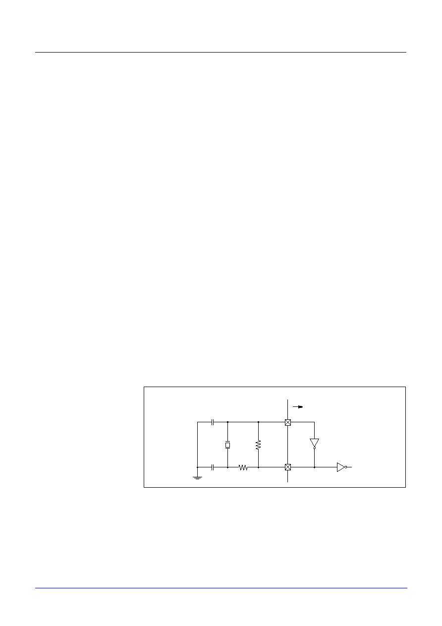
Introduction
1.11 Crystal Oscillator Consideration
Samsung ASIC
1-45
STDL130
1.11
Crystal Oscillator
Consideration
1.11.1 OVERVIEW
The STDL130 library contains a cell commonly referred to as an on-chip
oscillator. The on-chip oscillator itself is not really an oscillator, but is an amplifier
suitable for being used as the feedback amplifier in an oscillator circuit. With
proper selection of off-chip components (crystal or ceramic resonator, resistors
and capacitors) this oscillator circuit performs better than other types of clock
oscillators.
It is very important to select suitable off-chip components for the on-chip oscillator
circuitry. It should be noted, however, that Samsung cannot assume
responsibility for writing specifications for the off-chip components or for the
performance of the finished oscillator design in production since the optimization
of the crystal oscillator circuit will be specific to a given application. Samsung
does, however, spec and guarantee the performance of the on-chip oscillator cell.
1.11.2 OSCILLATOR DESIGN CONSIDERATIONS
SoC designers have a number of options for clocking the system. A primary
decision is whether to use an on-chip oscillator or an external oscillator. If the
choice is to use an on-chip oscillator, the designer must then choose the type of
oscillator and off-chip component values. These decisions will be based on both
economic and technical requirements.The following section discusses some of
the factors to be considered.
1.11.2.1 On-Chip Oscillator
In most cases, the on-chip oscillator with the appropriate external components
provides the most economical solution to the clocking problem. Exceptions may
arise in server environments when frequency tolerances are tighter than about
0.01%.
The external components commonly used for the oscillator circuit are a positive
reactance (normal crystal oscillator), two capacitors, C1 and C2, and two
resistors, Rf and Rx, as shown in the figure below.
Figure 1-15.
CMOS Oscillator
1.11.2.2 Crystal Specifications
Specifications for an appropriate crystal are not very critical. Any fundamental
mode crystal of medium or better quality can be used. Crystal resistance affects
start-up time and steady state amplitude but can be compensated by the choice
of C1 and C2, however, the lower the crystal resistance, the better. A discussion
of external R and C components follows below.
C1
C2
Rx
Rf
PADA
PADY
Feedback
Inside of a Chip
Amplifier

1.11 Crystal Oscillator Consideration
Introduction
STDL130
1-46
Samsung ASIC
1.11.2.3 Oscillation Frequency
The oscillation frequency is mainly determined by the crystal. The on-chip
oscillator has little effect on the frequency.
The influence of the on-chip oscillator on frequency results from its input and
output (pin-to-ground) capacitances which parallel C1 and C2, and the PADA-to-
PADY (pin-to-pin) capacitance which parallels the crystal. The input and pin-to-
pin capacitances are about 7pF each.
1.11.2.4 C1 and C2 Selection
Optimal values for C1 and C2 depend on whether a quartz crystal or ceramic
resonator is used, and on application-specific requirements for start-up time and
frequency tolerance.
Start-up time is sometimes more critical in microcontroller systems than
frequency stability because of various reset and initialization requirements.
Accuracy of the oscillator frequency is less commonly critical, as when the
oscillator is being used as a time base. As a general rule, fast start-up and stable
frequency tend to pull the oscillator design in opposite directions.
Considerations of both start-up time and frequency stability over temperature
suggest that C1 and C2 should be about equal and at least 15pF (but they don't
have to be either).
Increasing the value of these capacitors above 40pF or 50pF improves frequency
stability, but also increases the start-up time. If the capacitors are too large
(several hundred pF), the oscillator won't start up at all.
1.11.2.5 Rf and Rx Selection
A large Rf (1M
) holds the on-chip oscillator (a CMOS inverter) ins it linear region
allowing it to oscillate. The inverter has a fairly low output resistance which de-
stabilizes the oscillator circuit. Rx of several k
is added to the feedback network,
as shown in Figure 1-15, to stabilize the oscillator circuit.
At higher oscillator frequencies, a 20pF or 30pF capacitor is sometimes used in
place of Rx to compensate for internal propagation delay.
1.11.3 PCB CONSIDERATIONS
Noise glitches arising at PADA or PADY pins at the wrong time can cause a
miscount in the internal clock-generating circuitry. These kinds of glitches can be
produced through capacitive coupling between the oscillator components and
PCB traces carrying digital signals with fast rise and fall times.
For this reason, the oscillator components should be mounted close to the chip
and have short, direct traces to the PADA, PADY, and VSS pins. If possible, use
dedicated V
SS
and V
DD
pins for the on-chip oscillator.
In addition, surrounding oscillator components with "quiet" traces (V
DD
and V
SS
)
will alleviate capacitive coupling to signals having fast edges. To minimize
inductive coupling, the PCB layout should minimize lead, wire, and trace lengths
for oscillator components.

Introduction
1.11 Crystal Oscillator Consideration
Samsung ASIC
1-47
STDL130
Paths that need to be checked are:
- PADA through the resonator to PADY;
- PADA through C1 to the V
SS
pin;
- PADY through C2 to the V
SS
pin.
It is not unusual to find that the ground ends of C1 and C2 connect to the V
SS
pin
through long traces on the board.
1.11.4 TROUBLESHOOTING OSCILLATOR PROBLEMS
The cause of an oscillator problem may be difficult to find. Belows are some
suggested things to investigate if an oscillator problem is detected.
There may be significant differences in stray capacitances between the test
fixture and the actual application, particularly if the actual application is on a multi-
layer board. This may result in an oscillator problem occurring in the test fixture
that will not occur on the board, or a problem occurring on the board that cannot
be duplicated on the test fixture.
Noise glitches not present in the test fixture but present on the application board
may be another cause for an oscillator problem. Capacitive coupling between the
oscillator circuitry and other signal should be investigated. Inductive coupling is
also possible if there is a lead, trace, or wire with a large current nearby.
Finally, it should not be overlooked that software problems can mimic the
symptoms of a slow-starting oscillator or incorrect frequency. Software should
also be invigilated.

2
Electrical Characteristics

Contents
DC Electrical Characteristics ......................................................................................... 2-1
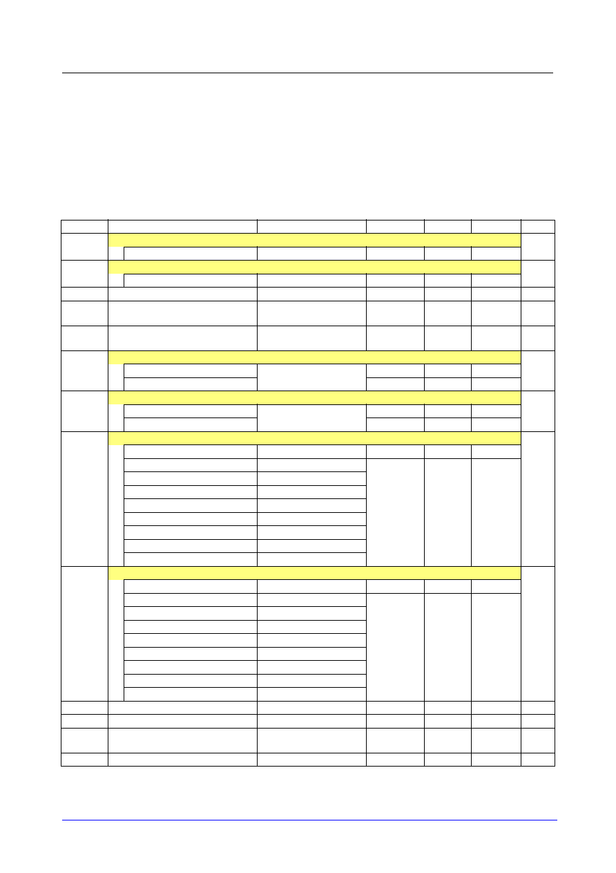
ELECTRICAL CHARACTERISTICS
DC ELECTRICAL CHARACTERISTICS
Samsung ASIC
2-1
STDL130
DC ELECTRICAL CHARACTERISTICS
The following tables define the DC electrical characteristics for the standard LVCMOS I/O buffers
described in Chapter 4: "Input/Output Cells." The DC electrical characteristics for oscillator and standard
bus interface I/O buffers such as USB and PCI follow the desciptions of those buffer cells in Chapter 4.
V
DD
= 1.8V
±
0.15V, Ta =
≠
40 to 85
∞
C, V
EXT
= 3.3V
±
0.3V (In case of 3.3V tolerant)
Symbol
Parameter
Condition
Min
Type
Max
Unit
V
IH
High level input voltage
V
LVCMOS interface
1.27
V
IL
Low level input voltage
V
LVCMOS interface
0.57
VT
Switching threshold
0.5V
DD
V
VT
+
Schmitt trigger, positive-going
threshold
CMOS
1.27
V
VT ≠
Schmitt trigger, negative-going
threshold
CMOS
0.57
V
I
IH
High level input current
µ
A
Input buffer
V
IN
= V
DD
≠10
10
Input buffer with pull-down
5
18
40
I
IL
Low level input current
µ
A
Input buffer
V
IN
= V
SS
≠10
10
Input buffer with pull-up
≠40
≠18
≠5
V
OH
High level output voltage
V
Type B1 to B24
I
OH
= ≠1
µ
A
V
DD
≠ 0.05
Type B1
I
OH
= ≠1mA
1.2
Type B2
I
OH
= ≠2mA
Type B4
I
OH
= ≠4mA
Type B8
I
OH
= ≠8mA
Type B12
I
OH
= ≠12mA
Type B16
I
OH
= ≠16mA
Type B20
I
OH
= ≠20mA
Type B24
I
OH
= ≠24mA
V
OL
Low level output voltage
V
Type B1 to B24
I
OL
= 1
µ
A
0.05
Type B1
I
OL
= 1mA
0.45
Type B2
I
OL
= 2mA
Type B4
I
OL
= 4mA
Type B8
I
OL
= 8mA
Type B12
I
OL
= 12mA
Type B16
I
OL
= 16mA
Type B20
I
OL
= 20mA
Type B24
I
OL
= 24mA
I
OZ
Tri-state output leakage current
V
OUT
=V
SS
or V
DD
≠10
10
µ
A
I
DD
Quiescent supply current
100
µ
A
C
IN
Input capacitance
Any input and
Bi-directional Buffers
4
pF
C
OUT
Output capacitance
Any output buffer
4
pF

DC ELECTRICAL CHARACTERISTICS
ELECTRICAL CHARACTERISTICS
STDL130
2-2
Samsung ASIC
V
DD
= 2.5V
±
0.2V, Ta =
≠
40 to 85
∞
C, V
EXT
= 5V
±
0.25V (In case of 5V tolerant)
Symbol
Parameter
Condition
Min
Type
Max
Unit
V
IH
High level input voltage
V
LVCMOS interface
1.7
V
IL
Low level input voltage
V
LVCMOS interface
0.7
VT
Switching threshold
0.5V
DD
V
VT
+
Schmitt trigger, positive-going
threshold
CMOS
1.7
V
VT ≠
Schmitt trigger, negative-going
threshold
CMOS
0.7
V
I
IH
High level input current
µ
A
Input buffer
V
IN
= V
DD
≠10
10
Input buffer with pull-down
10
25
50
I
IL
Low level input current
µ
A
Input buffer
V
IN
= V
SS
≠10
10
Input buffer with pull-up
≠50
≠25
≠10
V
OH
High level output voltage
V
Type B1 to B24
I
OH
= ≠1
µ
A
V
DD
≠ 0.05
Type B1
I
OH
= ≠1mA
1.9
Type B2
I
OH
= ≠2mA
Type B4
I
OH
= ≠4mA
Type B8
I
OH
= ≠8mA
Type B12
I
OH
= ≠12mA
Type B16
I
OH
= ≠16mA
Type B20
I
OH
= ≠20mA
Type B24
I
OH
= ≠24mA
V
OL
Low level output voltage
V
Type B1 to B24
I
OL
= 1
µ
A
0.05
Type B1
I
OL
= 1mA
0.4
Type B2
I
OL
= 2mA
Type B4
I
OL
= 4mA
Type B8
I
OL
= 8mA
Type B12
I
OL
= 12mA
Type B16
I
OL
= 16mA
Type B20
I
OL
= 20mA
Type B24
I
OL
= 24mA
I
OZ
Tri-state output leakage current
V
OUT
=V
SS
or V
DD
≠10
10
µ
A
I
DD
Quiescent supply current
100
µ
A
C
IN
Input capacitance
Any input and
Bi-directional buffers
4
pF
C
OUT
Output capacitance
Any output buffer
4
pF
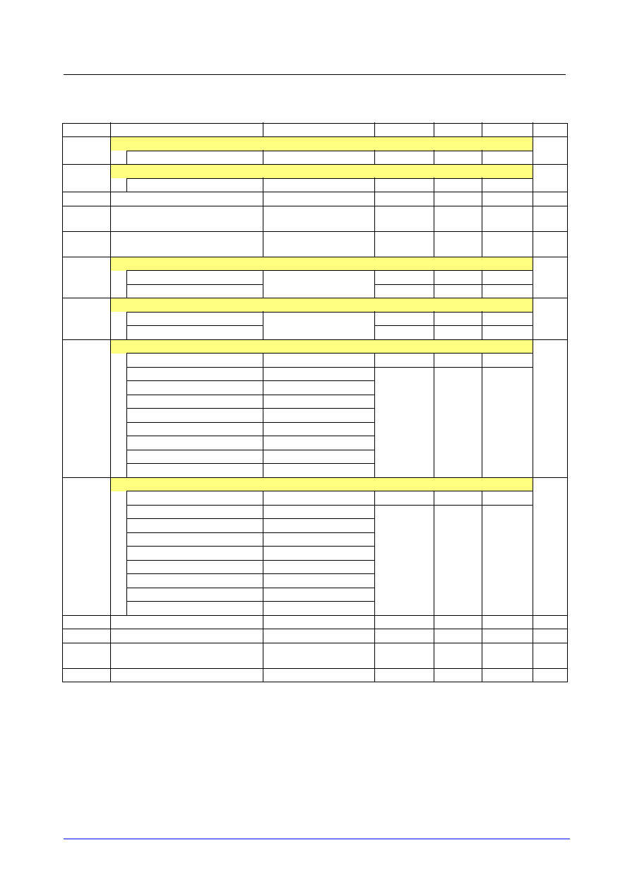
ELECTRICAL CHARACTERISTICS
DC ELECTRICAL CHARACTERISTICS
Samsung ASIC
2-3
STDL130
V
DD
= 3.3V
±
0.3V, Ta =
≠
40 to 85
∞
C, V
EXT
= 5V
±
0.25V (In case of 5V tolerant)
Symbol
Parameter
Condition
Min
Type
Max
Unit
V
IH
High level input voltage
V
LVCMOS interface
2.0
V
IL
Low level input voltage
V
LVCMOS interface
0.8
VT
Switching threshold
1.4
V
VT
+
Schmitt trigger, positive-going
threshold
CMOS
2.0
V
VT ≠
Schmitt trigger, negative-going
threshold
CMOS
0.8
V
I
IH
High level input current
µ
A
Input buffer
V
IN
= V
DD
≠10
10
Input buffer with pull-down
10
33
60
I
IL
Low level input current
µ
A
Input buffer
V
IN
= V
SS
≠10
10
Input buffer with pull-up
≠60
≠33
≠10
V
OH
High level output voltage
V
Type B1 to B24
I
OH
= ≠1
µ
A
V
DD
≠ 0.05
Type B1
I
OH
= ≠1mA
2.4
Type B2
I
OH
= ≠2mA
Type B4
I
OH
= ≠4mA
Type B8
I
OH
= ≠8mA
Type B12
I
OH
= ≠12mA
Type B16
I
OH
= ≠16mA
Type B20
I
OH
= ≠20mA
Type B24
I
OH
= ≠24mA
V
OL
Low level output voltage
V
Type B1 to B24
I
OL
= 1
µ
A
0.05
Type B1
I
OL
= 1mA
0.4
Type B2
I
OL
= 2mA
Type B4
I
OL
= 4mA
Type B8
I
OL
= 8mA
Type B12
I
OL
= 12mA
Type B16
I
OL
= 16mA
Type B20
I
OL
= 20mA
Type B24
I
OL
= 24mA
I
OZ
Tri-state output leakage current
V
OUT
=V
SS
or V
DD
≠10
10
µ
A
I
DD
Quiescent supply current
100
µ
A
C
IN
Input capacitance
Any input and
Bi-directional buffers
4
pF
C
OUT
Output capacitance
Any output buffer
4
pF
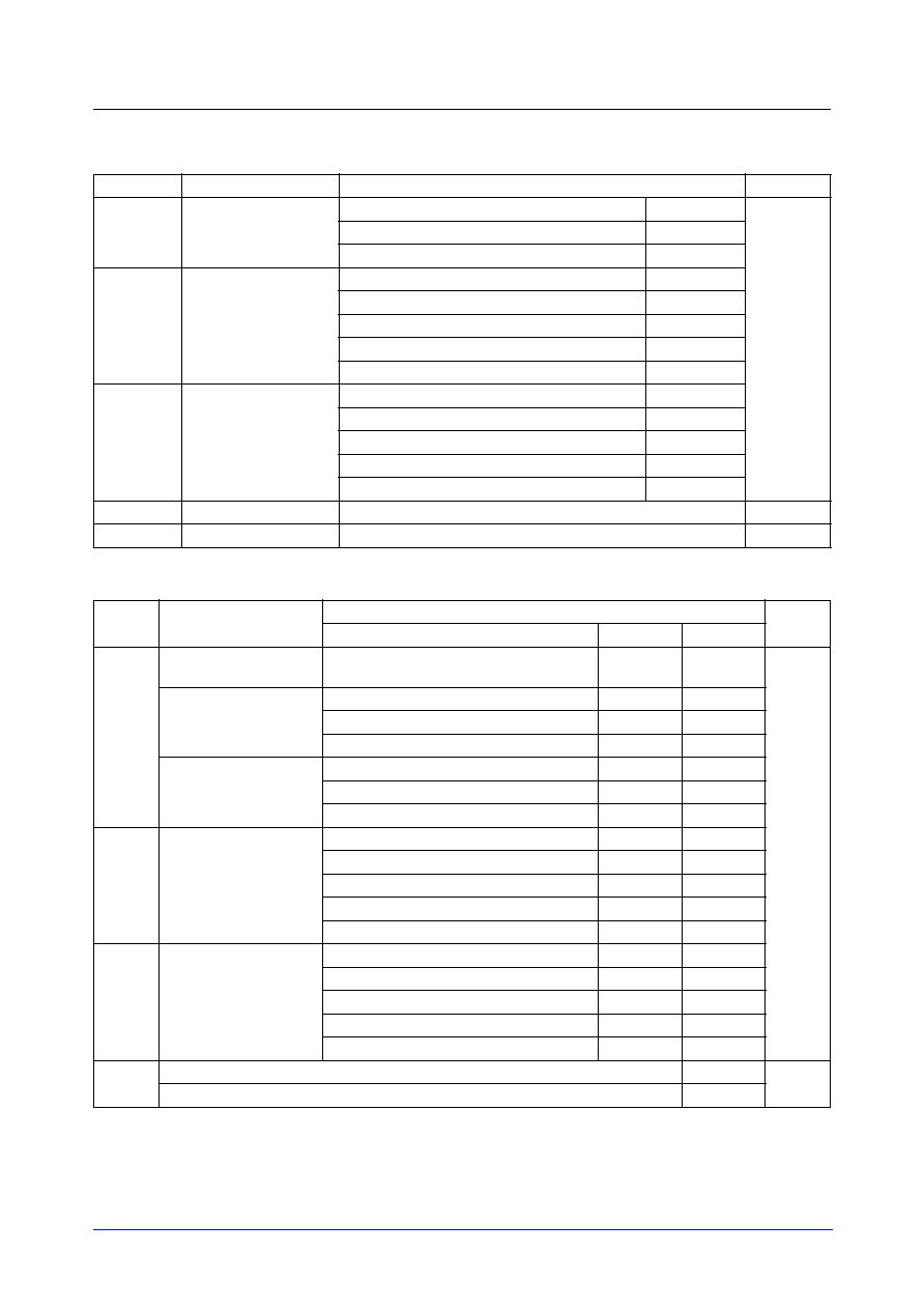
DC ELECTRICAL CHARACTERISTICS
ELECTRICAL CHARACTERISTICS
STDL130
2-4
Samsung ASIC
Absolute Maximum Ratings
Recommended Operating Conditions
Symbol
Parameter
Rating
Unit
V
DD
DC supply voltage
1.8V V
DD
2.7
V
2.5V V
DD
3.8
3.3V V
DD
4.8
V
IN
DC input voltage
1.8V input buffer
2.7
2.5V input buffer
3.8
3.3V input buffer
4.8
1.8V interface/3.3V tolerant input buffer
3.8
3.3V interface/5V tolerant input buffer
6.5
V
OUT
DC output voltage
1.8V output buffer
2.7
2.5V output buffer
3.8
3.3V output buffer
4.8
1.8V interface/3.3V tolerant output buffer
3.8
3.3V interface/5V tolerant output buffer
6.5
I
Latch
Latch up current
±
200
mA
T
STG
Storage temperature
≠65 to 150
∞
C
Symbol
Parameter
Rating
Unit
Min
Max
V
DD
DC supply voltage for
internal (=V
DDIN
)
1.8V V
DD
1.65
1.95
V
DC supply voltage for
I/O block (=V
DDIO
)
1.8V V
DD
1.65
1.95
2.5V V
DD
2.3
2.7
3.3V V
DD
3.0
3.6
DC supply voltage for
analog core (=V
DDA
)
1.8V V
DD
1.8 ≠ 5%
1.8 + 5%
2.5V V
DD
2.5 ≠ 5%
2.5 + 5%
3.3V V
DD
3.3 ≠ 5%
3.3 + 5%
V
IN
DC input voltage
1.8V input buffer
≠0.1
V
DDIO
+0.15
2.5V input buffer
≠0.2
V
DDIO
+0.2
3.3V input buffer
≠0.3
V
DDIO
+0.3
1.8V interface/3.3V tolerant input buffer
≠0.1
3.6
3.3V interface/5V tolerant input buffer
≠0.3
5.5
V
OUT
DC output voltage
1.8V output buffer
≠0.1
V
DDIO
+0.15
2.5V output buffer
≠0.2
V
DDIO
+0.2
3.3V output buffer
≠0.3
V
DDIO
+0.3
1.8V interface/3.3V tolerant output buffer
≠0.1
3.6
3.3V interface/5V tolerant output buffer
≠0.3
5.5
T
A
Commercial temperature range
0 to 70
∞
C
Industrial temperature range
≠40 to 85

3
Internal Macrocells

Contents
Overview .............................................................................................................................. 3-1
Summary Tables................................................................................................................... 3-2
Logic Cells............................................................................................................................ 3-7
Flip-Flops.............................................................................................................................. 3-219
Latches................................................................................................................................. 3-296
Bus Holder............................................................................................................................ 3-321
Internal Clock Drivers ........................................................................................................... 3-322
Adders .................................................................................................................................. 3-324
Multiplexers .......................................................................................................................... 3-329
Integrated Clock-Gating Cells............................................................................................... 3-342

INTERNAL MACROCELLS
OVERVIEW
Samsung ASIC
3-1
STDL130
OVERVIEW
This chapter contains data sheets for standard logic macrocells; combinational logic cells, flip-flops, latches,
bus holder, internal clock drivers, decoders, adders, multiplexers and integrated clock-gating cells. The
electrical characteristics of each cell follow each cell's description. A summary table in the following pages
list the entire STDL130 standard logic macrocell library by the cell type along with the cell description page
number. Moreover, each section begins with a table containing a brief functional description of each cell in
that section.
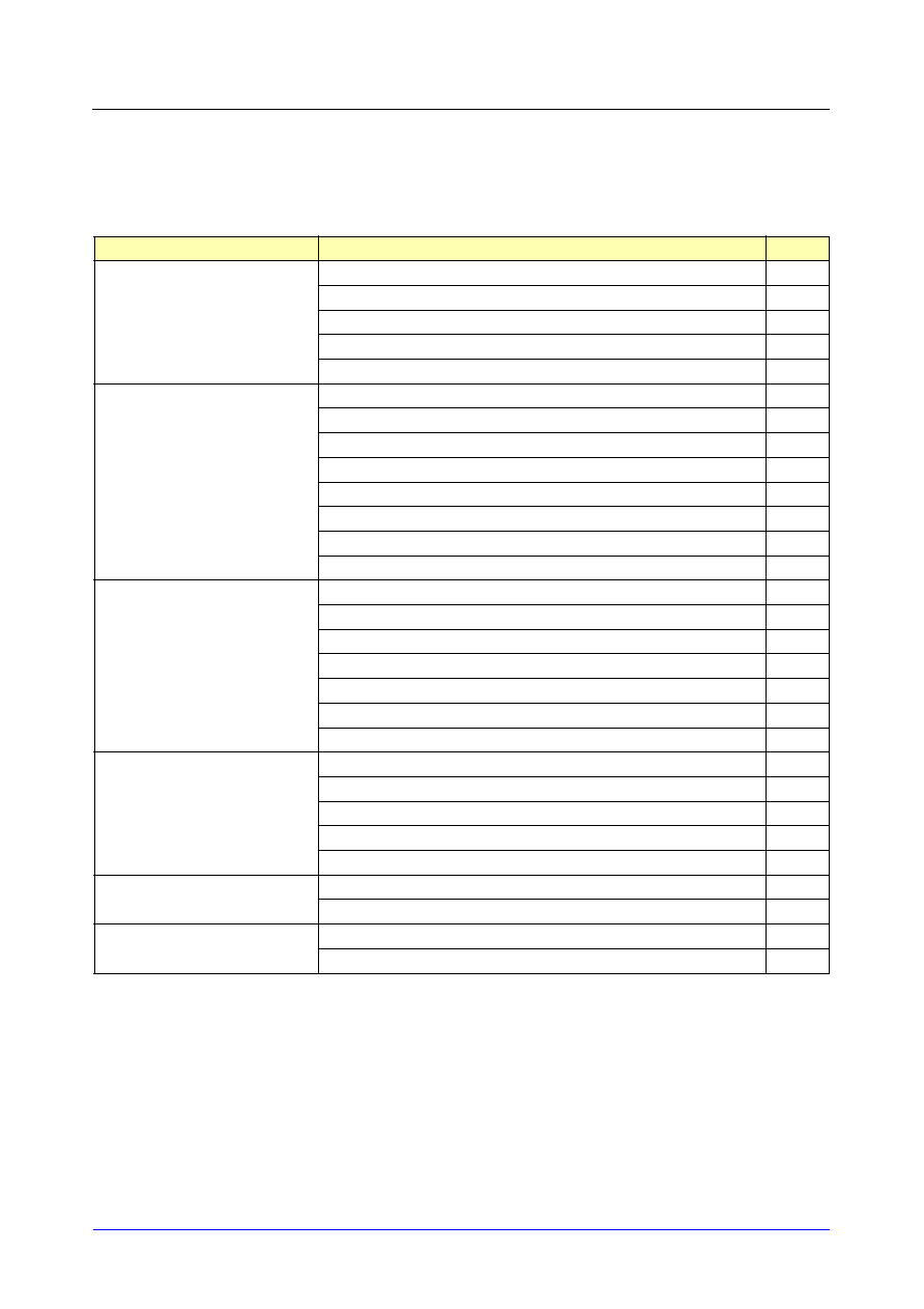
SUMMARY TABLES
INTERNAL MACROCELLS
STDL130
3-2
Samsung ASIC
SUMMARY TABLES
Logic Cells
Cell Type
Cell Name
Page
AND Cell
AD2_LP/AD2D2_LP/AD2D4_LP/AD2D8_LP
3-14
AD2B_LP/AD2BD2_LP/AD2BD4_LP/AD2BD8_LP
3-16
AD3_LP/AD3D2_LP/AD3D4_LP
3-18
AD4_LP/AD4D2_LP/AD4D4_LP
3-20
AD5_LP/AD5D2_LP/AD5D4_LP
3-22
NAND Cell
ND2_LP/ND2D2_LP/ND2D4_LP/ND2D8_LP
3-25
ND2B_LP/ND2BD2_LP/ND2BD4_LP/ND2BD8_LP
3-27
ND3_LP/ND3D2_LP/ND3D4_LP/ND3D8_LP
3-29
ND3B_LP/ND3BD2_LP/ND3BD4_LP/ND3BD8_LP
3-32
ND4_LP/ND4D2_LP/ND4D4_LP
3-35
ND5_LP/ND5D2_LP/ND5D4_LP
3-37
ND6_LP/ND6D2_LP/ND6D4_LP
3-40
ND8_LP/ND8D2_LP/ND8D4_LP
3-44
NOR Cell
NR2_LP/NR2A_LP/NR2D2_LP/NR2D4_LP/NR2D8_LP
3-48
NR2B_LP/NR2BD2_LP/NR2BD4_LP/NR2BD8_LP
3-50
NR3_LP/NR3A_LP/NR3D2_LP/NR3D4_LP
3-52
NR4_LP/NR4D2_LP/NR4D4_LP
3-55
NR5_LP/NR5D2_LP/NR5D4_LP
3-57
NR6_LP/NR6D2_LP/NR6D4_LP
3-61
NR8_LP/NR8D2_LP/NR8D4_LP
3-65
OR Cell
OR2_LP/OR2D2_LP/OR2D4_LP/OR2D8_LP
3-69
OR2B_LP/OR2BD2_LP/OR2BD4_LP/OR2BD8_LP
3-71
OR3_LP/OR3D3_LP/OR3D4_LP
3-73
OR4_LP/OR4D2_LP/OR4D4_LP
3-75
OR5_LP/OR5D2_LP/OR5D4_LP
3-77
Exclusive-NOR Cell
XN2_LP/XN2D2_LP/XN2D4_LP
3-80
XN3_LP/XN3D2_LP/XN3D4_LP
3-82
Exclusive-OR Cell
XO2_LP/XO2D2_LP/XO2D4_LP
3-84
XO3_LP/XO3D2_LP/XO3D4_LP
3-86
INTERNAL MACROCELLS
SUMMARY TABLES
Samsung ASIC
3-3
STDL130
Combinational Cell of AND
and NOR
AO21_LP/AO21D2_LP/AO21D4_LP
3-88
AO211_LP/AO211D2_LP/AO211D4_LP
3-90
AO2111_LP/AO2111D2_LP
3-92
AO22_LP/AO22D2_LP/AO22D4_LP
3-94
AO22A_LP
3-96
AO221_LP/AO221D2_LP/AO221D4_LP
3-97
AO222_LP/AO222D2_LP/AO222D4_LP
3-100
AO222A_LP
3-104
AO2222_LP/AO2222D2_LP/AO2222D4_LP
3-105
AO31_LP/AO31D2_LP/AO31D4_LP
3-109
AO311_LP
3-111
AO3111_LP
3-112
AO32_LP/AO32D2_LP
3-113
AO321_LP
3-115
AO322_LP
3-116
AO33_LP
3-118
AO331_LP
3-120
AO332_LP
3-122
Combinational Cell of OR and
NAND
OA21_LP/OA21D2_LP/OA21D4_LP
3-124
OA211_LP/OA211D2_LP/OA211D4_LP
3-126
OA2111_LP/OA2111D2_LP
3-128
OA22_LP/OA22D2_LP/OA22D4_LP
3-130
OA22A_LP/OA22D2A_LP/OA22D4A_LP
3-132
OA221_LP/OA221D2_LP/OA221D4_LP
3-134
OA222_LP/OA222D2_LP/OA222D4_LP
3-137
OA2222_LP/OA2222D2_LP/OA2222D4_LP
3-141
OA31_LP/OA31D2_LP/OA31D4_LP
3-145
OA311_LP
3-147
OA3111_LP
3-148
OA32_LP
3-149
OA321_LP
3-150
OA322_LP
3-151
OA33_LP
3-153
Cell Type
Cell Name
Page
SUMMARY TABLES
INTERNAL MACROCELLS
STDL130
3-4
Samsung ASIC
Complex Cells
SCG1_LP/SCG1D2_LP
3-154
SCG2_LP/SCG2D2_LP/SCG2D4_LP
3-157
SCG3_LP/SCG3D2_LP/SCG3D4_LP
3-159
SCG4_LP/SCG4D2_LP/SCG4D4_LP
3-162
SCG5_LP/SCG5D2_LP/SCG5D4_LP
3-166
SCG6_LP/SCG6D2_LP
3-170
SCG7_LP/SCG7D2_LP
3-172
SCG8_LP/SCG8D2_LP
3-174
SCG9_LP/SCG9D2_LP
3-176
SCG10_LP/SCG10D2_LP
3-178
SCG11_LP/SCG11D2_LP
3-180
SCG12_LP/SCG12D2_LP/SCG12D4_LP
3-182
SCG13_LP/SCG13D2_LP
3-184
SCG14_LP/SCG14D2_LP
3-186
SCG15_LP/SCG15D2_LP
3-188
SCG16_LP/SCG16D2_LP
3-190
SCG17_LP/SCG17D2_LP
3-192
Complex Cells
SCG18_LP/SCG18D2_LP
3-194
SCG19_LP/SCG19D2_LP
3-196
SCG20_LP/SCG20D2_LP
3-198
SCG21_LP/SCG21D2_LP
3-200
SCG22_LP/SCG22D2_LP
3-202
Delay Cells
DL1D2_LP
3-204
DL2D2_LP
3-205
DL5D2_LP
3-206
DL10D2_LP
3-207
Inverter
IV_LP/IVD2_LP/IVD3_LP/IVD4_LP/IVD6_LP/IVD8_LP/
IVD16_LP/IVD24_LP
3-208
Inverting Tri-State Buffer
IVT_LP/IVTD2_LP/IVTD4_LP/IVTD8_LP/IVTD16_LP
3-211
Non-Inverting Buffer
NID_LP/NID2_LP/NID3_LP/NID4_LP/NID6_LP/
NID8_LP/NID16_LP/NID24_LP
3-213
NIT_LP/NITD2_LP/NITD4_LP/NITD8_LP/NITD16_LP
3-216
Cell Type
Cell Name
Page
INTERNAL MACROCELLS
SUMMARY TABLES
Samsung ASIC
3-5
STDL130
Flip-Flops
Cell Type
Cell Name
Page
D Flip-Flop
FD1_LP/FD1D2_LP
3-221
FD1S_LP/FD1SD2_LP
3-223
FD1SQ_LP/FD1SQD2_LP
3-225
FD1Q_LP/FD1QD2_LP
3-227
D Flip-Flop with Reset
FD2_LP/FD2D2_LP
3-229
FD2S_LP/FD2SD2_LP
3-231
FD2SQ_LP/FD2SQD2_LP
3-233
FD2Q_LP/FD2QD2_LP
3-235
D Flip-Flop with Set
FD3_LP/FD3D2_LP
3-237
FD3S_LP/FD3SD2_LP
3-239
FD3SQ_LP/FD3SQD2_LP
3-241
FD3Q_LP/FD3QD2_LP
3-243
D Flip-Flop with Reset, Set
FD4_LP/FD4D2_LP
3-245
FD4S_LP/FD4SD2_LP
3-248
FD4SQ_LP/FD4SQD2_LP
3-252
FD4Q_LP/FD4QD2_LP
3-255
D Flip-Flop with Negative Edge Trigger
FD5_LP/FD5D2_LP
3-257
FD5S_LP/FD5SD2_LP
3-259
FD6_LP/FD6D2_LP
3-261
FD6S_LP/FD6SD2_LP
3-263
FD7_LP/FD7D2_LP
3-265
FD7S_LP/FD7SD2_LP
3-267
FD8_LP/FD8D2_LP
3-269
FD8S_LP/FD8SD2_LP
3-272
D Flip-Flop with Synchronous Clear
FDS2_LP/FDS2D2_LP
3-276
FDS2S_LP/FDS2SD2_LP
3-278
FDS3_LP/FDS3D2_LP
3-280
FDS3S_LP/FDS3SD2_LP
3-282
JK Flip-Flop
FJ2_LP/FJ2D2_LP
3-284
FJ2S_LP/FJ2SD2_LP
3-286
FJ4_LP/FJ4D2_LP
3-288
FJ4S_LP/FJ4SD2_LP
3-291
Toggle Flip-Flop
FT2_LP/FT2D2_LP
3-294
SUMMARY TABLES
INTERNAL MACROCELLS
STDL130
3-6
Samsung ASIC
Latches
Bus Holder
Internal Clock Drivers
Adders
Multiplexers
Integrated Clock-Gating Cells
Cell Type
Cell Name
Page
D Latch with Active High
LD1_LP/LD1D2_LP
3-297
LD1Q_LP/LD1QD2_LP
3-299
LD2_LP/LD2D2_LP
3-301
LD2Q_LP/LD2QD2_LP
3-304
LD3_LP/LD3D2_LP
3-306
LD4_LP/LD4D2_LP
3-309
D Latch with Active Low
LD5_LP/LD5D2_LP
3-312
LD5Q_LP/LD5QD2_LP
3-314
LD6_LP/LD6D2_LP
3-316
LD6Q_LP/LD6QD2_LP
3-319
Cell Type
Cell Name
Page
Bus Holder
BUSHOLDER_LP
3-321
Cell Type
Cell Name
Page
Internal Clock Drivers
CK2_LP/CK4_LP/CK6_LP/CK8_LP
3-322
Cell Type
Cell Name
Page
Full Adder
FA_LP/FAD2_LP
3-325
Half Adder
HA_LP/HAD2_LP
3-327
Cell Type
Cell Name
Page
2 > 1 Non-Inverting Mux
MX2_LP/MX2D2_LP/MX2D4_LP
3-330
2 > 1 Inverting Mux
MX2I_LP/MX2ID2_LP/MX2ID4_LP
3-333
MX2IA_LP/MX2ID2A_LP/MX2ID4A_LP
3-335
4 > 1 Non-Inverting Mux
MX4_LP/MX4D2_LP/MX4D4_LP
3-338
Cell Type
Cell Name
Page
Integrated Clock-Gating Cells
CGLN_LP/CGLND2_LP/CGLND4_LP
3-343
CGLP_LP/CGLPD2_LP/CGLPD4_LP
3-346
Samsung ASIC
3-7
STDL131
LOGIC CELLS
Cell Names & Function Descriptions
Cell Name
Function Description
AD2_LP
2-Input AND with 1X Drive
AD2D2_LP
2-Input AND with 2X Drive
AD2D4_LP
2-Input AND with 4X Drive
AD2D8_LP
2-Input AND with 8X Drive
AD2B_LP
2-Input AND with one Inverted Input, 1X Drive
AD2BD2_LP
2-Input AND with one Inverted Input, 2X Drive
AD2BD4_LP
2-Input AND with one Inverted Input, 4X Drive
AD2BD8_LP
2-Input AND with one Inverted Input, 8X Drive
AD3_LP
3-Input AND with 1X Drive
AD3D2_LP
3-Input AND with 2X Drive
AD3D4_LP
3-Input AND with 4X Drive
AD4_LP
4-Input AND with 1X Drive
AD4D2_LP
4-Input AND with 2X Drive
AD4D4_LP
4-Input AND with 4X Drive
AD5_LP
5-Input AND with 1X Drive
AD5D2_LP
5-Input AND with 2X Drive
AD5D4_LP
5-Input AND with 4X Drive
ND2_LP
2-Input NAND with 1X Drive
ND2D2_LP
2-Input NAND with 2X Drive
ND2D4_LP
2-Input NAND with 4X Drive
ND2D8_LP
2-Input NAND with 8X Drive
ND2B_LP
2-Input NAND with one Inverted Input, 1X Drive
ND2BD2_LP
2-Input NAND with one Inverted Input, 2X Drive
ND2BD4_LP
2-Input NAND with one Inverted Input, 4X Drive
ND2BD8_LP
2-Input NAND with one Inverted Input, 8X Drive
ND3_LP
3-Input NAND with 1X Drive
ND3D2_LP
3-Input NAND with 2X Drive
ND3D4_LP
3-Input NAND with 4X Drive
ND3D8_LP
3-Input NAND with 8X Drive
ND3B_LP
3-Input NAND with one Inverted Input, 1X Drive
ND3BD2_LP
3-Input NAND with one Inverted Input, 2X Drive
ND3BD4_LP
3-Input NAND with one Inverted Input, 4X Drive
ND3BD8_LP
3-Input NAND with one Inverted Input, 8X Drive
ND4_LP
4-Input NAND with 1X Drive
ND4D2_LP
4-Input NAND with 2X Drive
ND4D4_LP
4-Input NAND with 4X Drive
ND5_LP
5-Input NAND with 1X Drive
ND5D2_LP
5-Input NAND with 2X Drive
STDL131
3-8
Samsung ASIC
ND5D4_LP
5-Input NAND with 4X Drive
ND6_LP
6-Input NAND with 1X Drive
ND6D2_LP
6-Input NAND with 2X Drive
ND6D4_LP
6-Input NAND with 4X Drive
ND8_LP
8-Input NAND with 1X Drive
ND8D2_LP
8-Input NAND with 2X Drive
ND8D4_LP
8-Input NAND with 4X Drive
NR2_LP
2-Input NOR with 1X Drive
NR2A_LP
NR2 with 2X P-Transistor, 1X N-Transistor
NR2D2_LP
2-Input NOR with 2X Drive
NR2D4_LP
2-Input NOR with 4X Drive
NR2D8_LP
2-Input NOR with 8X Drive
NR2B_LP
2-Input NOR with one Inverted Input, 1X Drive
NR2BD2_LP
2-Input NOR with one Inverted Input, 2X Drive
NR2BD4_LP
2-Input NOR with one Inverted Input, 4X Drive
NR2BD8_LP
2-Input NOR with one Inverted Input, 8X Drive
NR3_LP
3-Input NOR with 1X Drive
NR3A_LP
3-Input NOR with 2X P-Transistor, 1X N-Transistor
NR3D2_LP
3-Input NOR with 2X Drive
NR3D4_LP
3-Input NOR with 4X Drive
NR4_LP
4-Input NOR with 1X Drive
NR4D2_LP
4-Input NOR with 2X Drive
NR4D4_LP
4-Input NOR with 4X Drive
NR5_LP
5-Input NOR with 1X Drive
NR5D2_LP
5-Input NOR with 2X Drive
NR5D4_LP
5-Input NOR with 4X Drive
NR6_LP
6-Input NOR with 1X Drive
NR6D2_LP
6-Input NOR with 2X Drive
NR6D4_LP
6-Input NOR with 4X Drive
NR8_LP
8-Input NOR with 1X Drive
NR8D2_LP
8-Input NOR with 2X Drive
NR8D4_LP
8-Input NOR with 4X Drive
OR2_LP
2-Input OR with 1X Drive
OR2D2_LP
2-Input OR with 2X Drive
OR2D4_LP
2-Input OR with 4X Drive
OR2D8_LP
2-Input OR with 8X Drive
OR2B_LP
2-Input OR with one Inverted Input, 1X Drive
OR2BD2_LP
2-Input OR with one Inverted Input, 2X Drive
Cell Name
Function Description
LOGIC CELLS
Cell Names & Function Descriptions (Continued)
Samsung ASIC
3-9
STDL131
OR2BD4_LP
2-Input OR with one Inverted Input, 4X Drive
OR2BD8_LP
2-Input OR with one Inverted Input, 8X Drive
OR3_LP
3-Input OR with 1X Drive
OR3D2_LP
3-Input OR with 2X Drive
OR3D4_LP
3-Input OR with 4X Drive
OR4_LP
4-Input OR with 1X Drive
OR4D2_LP
4-Input OR with 2X Drive
OR4D4_LP
4-Input OR with 4X Drive
OR5_LP
5-Input OR with 1X Drive
OR5D2_LP
5-Input OR with 2X Drive
OR5D4_LP
5-Input OR with 4X Drive
XN2_LP
2-Input Exclusive-NOR with 1X Drive
XN2D2_LP
2-Input Exclusive-NOR with 2X Drive
XN2D4_LP
2-Input Exclusive-NOR with 4X Drive
XN3_LP
3-Input Exclusive-NOR with 1X Drive
XN3D2_LP
3-Input Exclusive-NOR with 2X Drive
XN3D4_LP
3-Input Exclusive-NOR with 4X Drive
XO2_LP
2-Input Exclusive-OR with 1X Drive
XO2D2_LP
2-Input Exclusive-OR with 2X Drive
XO2D4_LP
2-Input Exclusive-OR with 4X Drive
XO3_LP
3-Input Exclusive-OR with 1X Drive
XO3D2_LP
3-Input Exclusive-OR with 2X Drive
XO3D4_LP
3-Input Exclusive-OR with 4X Drive
AO21_LP
2-AND into 2-NOR with 1X Drive
AO21D2_LP
2-AND into 2-NOR with 2X Drive
AO21D4_LP
2-AND into 2-NOR with 4X Drive
AO211_LP
2-AND into 3-NOR with 1X Drive
AO211D2_LP
2-AND into 3-NOR with 2X Drive
AO211D4_LP
2-AND into 3-NOR with 4X Drive
AO2111_LP
2-AND into 4-NOR with 1X Drive
AO2111D2_LP
2-AND into 4-NOR with 2X Drive
AO22_LP
Two 2-ANDs into 2-NOR with 1X Drive
AO22D2_LP
Two 2-ANDs into 2-NOR with 2X Drive
AO22D4_LP
Two 2-ANDs into 2-NOR with 4X Drive
AO22A_LP
2-AND and 2-NOR into 2-NOR with 1X Drive
AO221_LP
Two 2-ANDs into 3-NOR with 1X Drive
AO221D2_LP
Two 2-ANDs into 3-NOR with 2X Drive
AO221D4_LP
Two 2-ANDs into 3-NOR with 4X Drive
Cell Name
Function Description
LOGIC CELLS
Cell Names & Function Descriptions (Continued)
STDL131
3-10
Samsung ASIC
LOGIC CELLS
Cell Names & Function Descriptions (Continued)
AO222_LP
Three 2-ANDs into 3-NOR with 1X Drive
AO222D2_LP
Three 2-ANDs into 3-NOR with 2X Drive
AO222D4_LP
Three 2-ANDs into 3-NOR with 4X Drive
AO222A_LP
Inverting 2-of-3 Majority with 1X Drive
AO2222_LP
Four 2-ANDs into 4-NOR with 1X Drive
AO2222D2_LP
Four 2-ANDs into 4-NOR with 2X Drive
AO2222D4_LP
Four 2-ANDs into 4-NOR with 4X Drive
AO31_LP
3-AND into 2-NOR with 1X Drive
AO31D2_LP
3-AND into 2-NOR with 2X Drive
AO31D4_LP
3-AND into 2-NOR with 4X Drive
AO311_LP
3-AND into 3-NOR with 1X Drive
AO3111_LP
3-AND into 4-NOR with 1X Drive
AO32_LP
3-AND and 2-AND into 2-NOR with 1X Drive
AO32D2_LP
3-AND and 2-AND into 2-NOR with 2X Drive
AO321_LP
3-AND and 2-AND into 3-NOR with 1X Drive
AO322_LP
3-AND and Two 2-ANDs into 3-NOR with 1X Drive
AO33_LP
Two 3-ANDs into 2-NOR with 1X Drive
AO331_LP
Two 3-ANDs into 3-NOR with 1X Drive
AO332_LP
Two 3-ANDs and 2-AND into 3-NOR with 1X Drive
OA21_LP
2-OR into 2-NAND with 1X Drive
OA21D2_LP
2-OR into 2-NAND with 2X Drive
OA21D4_LP
2-OR into 2-NAND with 4X Drive
OA211_LP
2-OR into 3-NAND with 1X Drive
OA211D2_LP
2-OR into 3-NAND with 2X Drive
OA211D4_LP
2-OR into 3-NAND with 4X Drive
OA2111_LP
2-OR into 4-NAND with 1X Drive
OA2111D2_LP
2-OR into 4-NAND with 2X Drive
OA22_LP
Two 2-ORs into 2-NAND with 1X Drive
OA22D2_LP
Two 2-ORs into 2-NAND with 2X Drive
OA22D4_LP
Two 2-ORs into 2-NAND with 4X Drive
OA22A_LP
2-OR and 2-NAND into 2-NAND with 1X Drive
OA22D2A_LP
2-OR and 2-NAND into 2-NAND with 2X Drive
OA22D4A_LP
2-OR and 2-NAND into 2-NAND with 4X Drive
OA221_LP
Two 2-ORs into 3-NAND with 1X Drive
OA221D2_LP
Two 2-ORs into 3-NAND with 2X Drive
OA221D4_LP
Two 2-ORs into 3-NAND with 4X Drive
OA222_LP
Three 2-ORs into 3-NAND with 1X Drive
OA222D2_LP
Three 2-ORs into 3-NAND with 2X Drive
Cell Name
Function Description
Samsung ASIC
3-11
STDL131
LOGIC CELLS
Cell Names & Function Descriptions (Continued)
OA222D4_LP
Three 2-ORs into 3-NAND with 4X Drive
OA2222_LP
Four 2-ORs into 4-NAND with 1X Drive
OA2222D2_LP
Four 2-ORs into 4-NAND with 2X Drive
OA2222D4_LP
Four 2-ORs into 4-NAND with 4X Drive
OA31_LP
3-OR into 2-NAND with 1X Drive
OA31D2_LP
3-OR into 2-NAND with 2X Drive
OA31D4_LP
3-OR into 2-NAND with 4X Drive
OA311_LP
3-OR into 3-NAND with 1X Drive
OA3111_LP
3-OR into 4-NAND with 1X Drive
OA32_LP
3-OR and 2-OR into 2-NAND with 1X Drive
OA321_LP
3-OR and 2-OR into 3-NAND with 1X Drive
OA322_LP
3-OR and Two 2-ORs into 3-NAND with 1X Drive
OA33_LP
Two 3-ORs into 2-NAND with 1X Drive
SCG1_LP
2-NAND and two (2-AND into 2-NOR)s into 3-NAND with 1X Drive
SCG1D2_LP
2-NAND and two (2-AND into 2-NOR)s into 3-NAND with 2X Drive
SCG2_LP
Two 2-ANDs into 2-OR with 1X Drive
SCG2D2_LP
Two 2-ANDs into 2-OR with 2X Drive
SCG2D4_LP
Two 2-ANDs into 2-OR with 4X Drive
SCG3_LP
Two 2-NANDs into 3-NAND with 1X Drive
SCG3D2_LP
Two 2-NANDs into 3-NAND with 2X Drive
SCG3D4_LP
Two 2-NANDs into 3-NAND with 4X Drive
SCG4_LP
Two (two 2-ANDs into 2-NOR)s into 2-NAND with 1X Drive
SCG4D2_LP
Two (two 2-ANDs into 2-NOR)s into 2-NAND with 2X Drive
SCG4D4_LP
Two (two 2-ANDs into 2-NOR)s into 2-NAND with 4X Drive
SCG5_LP
Three 2-ANDs into 3-OR with 1X Drive
SCG5D2_LP
Three 2-ANDs into 3-OR with 2X Drive
SCG5D4_LP
Three 2-ANDs into 3-OR with 4X Drive
SCG6_LP
2-AND into 2-OR with 1X Drive
SCG6D2_LP
2-AND into 2-OR with 2X Drive
SCG7_LP
2-NAND and (2-AND into 2-NOR) into 2-NAND with 1X Drive
SCG7D2_LP
2-NAND and (2-AND into 2-NOR) into 2-NAND with 2X Drive
SCG8_LP
2-AND into 3-OR with 1X Drive
SCG8D2_LP
2-AND into 3-OR with 2X Drive
SCG9_LP
2-OR into 2-AND with 1X Drive
SCG9D2_LP
2-OR into 2-AND with 2X Drive
SCG10_LP
Two 2-ORs into 2-AND with 1X Drive
SCG10D2_LP
Two 2-ORs into 2-AND with 2X Drive
SCG11_LP
Two 2-NORs into 3-NOR with 1X Drive
Cell Name
Function Description

Samsung ASIC
3-12
STDL131
LOGIC CELLS
Cell Names & Function Descriptions (Continued)
Cell Name
Function Description
SCG11D2_LP
Two 2-NORs into 3-NOR with 2X Drive
SCG12_LP
2-NAND into 2-NOR with 1X Drive
SCG12D2_LP
2-NAND into 2-NOR with 2X Drive
SCG12D4_LP
2-NAND into 2-NOR with 4X Drive
SCG13_LP
2-NOR into 2-NAND with 1X Drive
SCG13D2_LP
2-NOR into 2-NAND with 2X Drive
SCG14_LP
2-NAND into 2-NAND with 1X Drive
SCG14D2_LP
2-NAND into 2-NAND with 2X Drive
SCG15_LP
2-NAND into 3-NAND with 1X Drive
SCG15D2_LP
2-NAND into 3-NAND with 2X Drive
SCG16_LP
2-OR with one inverted input into 2-NAND with 1X Drive
SCG16D2_LP
2-OR with one inverted input into 2-NAND with 2X Drive
SCG17_LP
2-AND into 2-NOR into 2-NAND with 1X Drive
SCG17D2_LP
2-AND into 2-NOR into 2-NAND with 2X Drive
SCG18_LP
2-AND into 2-NOR into 3-NAND with 1X Drive
SCG18D2_LP
2-AND into 2-NOR into 3-NAND with 2X Drive
SCG19_LP
2-AND into 2-AND into 2-NOR with 1X Drive
SCG19D2_LP
2-AND into 2-AND into 2-NOR with 2X Drive
SCG20_LP
2-NOR into 2-NOR with 1X Drive
SCG20D2_LP
2-NOR into 2-NOR with 2X Drive
SCG21_LP
2-NOR into 3-NOR with 1X Drive
SCG21D2_LP
2-NOR into 3-NOR with 2X Drive
SCG22_LP
2-NAND into 2-OR into 2-NAND with 1X Drive
SCG22D2_LP
2-NAND into 2-OR into 2-NAND with 2X Drive
DL1D2_LP
1ns Delay Cell with 2X Drive
DL2D2_LP
2ns Delay Cell with 2X Drive
DL5D2_LP
5ns Delay Cell with 2X Drive
DL10D2_LP
10ns Delay Cell with 2X Drive
IV_LP
Inverter with 1X Drive
IVD2_LP
Inverter with 2X Drive
IVD3_LP
Inverter with 3X Drive
IVD4_LP
Inverter with 4X Drive
IVD6_LP
Inverter with 6X Drive
IVD8_LP
Inverter with 8X Drive
IVD16_LP
Inverter with 16X Drive
IVD24_LP
Inverter with 24X Drive
IVT_LP
Inverting Tri-State Buffer with Enable High, 1X Drive
IVTD2_LP
Inverting Tri-State Buffer with Enable High, 2X Drive
Samsung ASIC
3-13
STDL131
LOGIC CELLS
Cell Names & Function Descriptions (Continued)
Cell Name
Function Description
IVTD4_LP
Inverting Tri-State Buffer with Enable High, 4X Drive
IVTD8_LP
Inverting Tri-State Buffer with Enable High, 8X Drive
IVTD16_LP
Inverting Tri-State Buffer with Enable High, 16X Drive
NID_LP
Non-Inverting Buffer with 1X Drive
NID2_LP
Non-Inverting Buffer with 2X Drive
NID3_LP
Non-Inverting Buffer with 3X Drive
NID4_LP
Non-Inverting Buffer with 4X Drive
NID6_LP
Non-Inverting Buffer with 6X Drive
NID8_LP
Non-Inverting Buffer with 8X Drive
NID16_LP
Non-Inverting Buffer with 16X Drive
NID24_LP
Non-Inverting Buffer with 24X Drive
NIT_LP
Non-Inverting Tri-State Buffer with Enable High, 1X Drive
NITD2_LP
Non-Inverting Tri-State Buffer with Enable High, 2X Drive
NITD4_LP
Non-Inverting Tri-State Buffer with Enable High, 4X Drive
NITD8_LP
Non-Inverting Tri-State Buffer with Enable High, 8X Drive
NITD16_LP
Non-Inverting Tri-State Buffer with Enable High, 16X Drive

STDL131
3-14
Samsung ASIC
AD2_LP/AD2D2_LP/AD2D4_LP/AD2D8_LP
2-Input AND with 1X/2X/4X/8X Drive
Logic Symbol
Cell Data
Switching Characteristics
(Typical process, 25
∞
C, 1.8V, t
R
/t
F
= 0.19ns, SL: Standard Load)
AD2_LP
AD2D2_LP
Input Load (SL)
Gate Count
AD2_LP
AD2D2_LP
AD2D4_LP
AD2D8_LP
AD2_LP
AD2D2_LP AD2D4_LP
AD2D8_LP
A
B
A
B
A
B
A
B
0.7
0.7
1.1
1.1
1.1
1.1
2.2
2.3
1.67
1.67
2.33
4.33
A
B
Y
Path
Parameter
Delay [ns]
SL = 2
Delay Equations [ns]
Group1*
Group2*
Group3*
A to Y
tR
0.104
0.055 + 0.025*SL
0.053 + 0.025*SL
0.046 + 0.026*SL
tF
0.073
0.039 + 0.017*SL
0.043 + 0.016*SL
0.039 + 0.017*SL
tPLH
0.170
0.142 + 0.014*SL
0.148 + 0.013*SL
0.150 + 0.012*SL
tPHL
0.169
0.146 + 0.012*SL
0.152 + 0.010*SL
0.156 + 0.010*SL
B to Y
tR
0.104
0.054 + 0.025*SL
0.053 + 0.025*SL
0.045 + 0.026*SL
tF
0.076
0.045 + 0.016*SL
0.043 + 0.016*SL
0.039 + 0.017*SL
tPLH
0.167
0.139 + 0.014*SL
0.145 + 0.013*SL
0.147 + 0.012*SL
tPHL
0.178
0.154 + 0.012*SL
0.161 + 0.010*SL
0.165 + 0.010*SL
*Group1 : SL < 4, *Group2 : 4 SL
<
<
=
= 8, *Group3 : 8 < SL
Path
Parameter
Delay [ns]
SL = 2
Delay Equations [ns]
Group1*
Group2*
Group3*
A to Y
tR
0.076
0.054 + 0.011*SL
0.049 + 0.012*SL
0.040 + 0.013*SL
tF
0.051
0.033 + 0.009*SL
0.035 + 0.008*SL
0.033 + 0.009*SL
tPLH
0.153
0.136 + 0.009*SL
0.143 + 0.007*SL
0.150 + 0.006*SL
tPHL
0.152
0.138 + 0.007*SL
0.144 + 0.005*SL
0.151 + 0.005*SL
B to Y
tR
0.076
0.054 + 0.011*SL
0.048 + 0.012*SL
0.041 + 0.013*SL
tF
0.054
0.036 + 0.009*SL
0.040 + 0.008*SL
0.036 + 0.008*SL
tPLH
0.150
0.133 + 0.009*SL
0.140 + 0.007*SL
0.146 + 0.006*SL
tPHL
0.160
0.146 + 0.007*SL
0.152 + 0.006*SL
0.159 + 0.005*SL
*Group1 : SL < 4, *Group2 : 4 SL
<
<
=
= 12, *Group3 : 12 < SL
Truth Table
A
B
Y
0
0
0
0
1
0
1
0
0
1
1
1

Samsung ASIC
3-15
STDL131
AD2_LP/AD2D2_LP/AD2D4_LP/AD2D8_LP
2-Input AND with 1X/2X/4X/8X Drive
Switching Characteristics
(Typical process, 25
∞
C, 1.8V, t
R
/t
F
= 0.19ns, SL: Standard Load)
AD2D4_LP
AD2D8_LP
Path
Parameter
Delay [ns]
SL = 2
Delay Equations [ns]
Group1*
Group2*
Group3*
A to Y
tR
0.074
0.060 + 0.007*SL
0.062 + 0.006*SL
0.060 + 0.006*SL
tF
0.056
0.046 + 0.005*SL
0.049 + 0.004*SL
0.050 + 0.004*SL
tPLH
0.185
0.173 + 0.006*SL
0.180 + 0.004*SL
0.196 + 0.003*SL
tPHL
0.180
0.170 + 0.005*SL
0.176 + 0.003*SL
0.191 + 0.003*SL
B to Y
tR
0.074
0.060 + 0.007*SL
0.064 + 0.006*SL
0.060 + 0.006*SL
tF
0.057
0.046 + 0.006*SL
0.051 + 0.004*SL
0.052 + 0.004*SL
tPLH
0.182
0.170 + 0.006*SL
0.177 + 0.004*SL
0.193 + 0.003*SL
tPHL
0.188
0.178 + 0.005*SL
0.184 + 0.003*SL
0.199 + 0.003*SL
*Group1 : SL < 4, *Group2 : 4 SL
<
<
=
= 20, *Group3 : 20 < SL
Path
Parameter
Delay [ns]
SL = 2
Delay Equations [ns]
Group1*
Group2*
Group3*
A to Y
tR
0.066
0.058 + 0.004*SL
0.061 + 0.003*SL
0.058 + 0.003*SL
tF
0.050
0.044 + 0.003*SL
0.048 + 0.002*SL
0.051 + 0.002*SL
tPLH
0.178
0.171 + 0.003*SL
0.175 + 0.002*SL
0.193 + 0.002*SL
tPHL
0.173
0.168 + 0.003*SL
0.172 + 0.002*SL
0.188 + 0.001*SL
B to Y
tR
0.066
0.060 + 0.003*SL
0.060 + 0.003*SL
0.060 + 0.003*SL
tF
0.051
0.046 + 0.003*SL
0.048 + 0.002*SL
0.052 + 0.002*SL
tPLH
0.174
0.168 + 0.003*SL
0.172 + 0.002*SL
0.190 + 0.002*SL
tPHL
0.181
0.176 + 0.003*SL
0.180 + 0.002*SL
0.196 + 0.001*SL
*Group1 : SL < 4, *Group2 : 4 SL
<
<
=
= 37, *Group3 : 37 < SL
STDL131
3-16
Samsung ASIC
AD2B_LP/AD2BD2_LP/AD2BD4_LP/AD2BD8_LP
2-Input AND with one Inverted Input, 1X/2X/4X/8X Drive
Logic Symbol
Cell Data
Switching Characteristics
(Typical process, 25
∞
C, 1.8V, t
R
/t
F
= 0.19ns, SL: Standard Load)
AD2B_LP
Input Load (SL)
Gate Count
AD2B_LP AD2BD2_LP AD2BD4_LP AD2BD8_LP AD2B_LP AD2BD2_LP AD2BD4_LP AD2BD8_LP
AN
B
AN
B
AN
B
AN
B
0.7
0.7
0.8
1.1
0.8
1.1
1.0
2.3
2.33
2.00
2.67
4.67
Truth Table
AN
B
Y
0
0
0
0
1
1
1
0
0
1
1
0
AN
B
Y
Path
Parameter
Delay [ns]
SL = 2
Delay Equations [ns]
Group1*
Group2*
Group3*
AN to Y
tR
0.104
0.055 + 0.024*SL
0.052 + 0.025*SL
0.045 + 0.026*SL
tF
0.073
0.040 + 0.017*SL
0.042 + 0.016*SL
0.038 + 0.017*SL
tPLH
0.240
0.212 + 0.014*SL
0.217 + 0.013*SL
0.220 + 0.012*SL
tPHL
0.198
0.175 + 0.012*SL
0.181 + 0.010*SL
0.186 + 0.010*SL
B to Y
tR
0.104
0.055 + 0.025*SL
0.054 + 0.025*SL
0.046 + 0.026*SL
tF
0.077
0.045 + 0.016*SL
0.044 + 0.016*SL
0.039 + 0.017*SL
tPLH
0.169
0.140 + 0.014*SL
0.146 + 0.013*SL
0.148 + 0.012*SL
tPHL
0.178
0.155 + 0.012*SL
0.161 + 0.010*SL
0.165 + 0.010*SL
*Group1 : SL < 4, *Group2 : 4 SL
<
<
=
= 8, *Group3 : 8 < SL
Samsung ASIC
3-17
STDL131
AD2B_LP/AD2BD2_LP/AD2BD4_LP/AD2BD8_LP
2-Input AND with one Inverted Input, 1X/2X/4X/8X Drive
Switching Characteristics
(Typical process, 25
∞
C, 1.8V, t
R
/t
F
= 0.19ns, SL: Standard Load)
AD2BD2_LP
AD2BD4_LP
AD2BD8_LP
Path
Parameter
Delay [ns]
SL = 2
Delay Equations [ns]
Group1*
Group2*
Group3*
AN to Y
tR
0.072
0.046 + 0.013*SL
0.047 + 0.013*SL
0.042 + 0.013*SL
tF
0.052
0.036 + 0.008*SL
0.035 + 0.008*SL
0.034 + 0.009*SL
tPLH
0.233
0.216 + 0.009*SL
0.223 + 0.007*SL
0.229 + 0.006*SL
tPHL
0.192
0.178 + 0.007*SL
0.184 + 0.006*SL
0.191 + 0.005*SL
B to Y
tR
0.077
0.055 + 0.011*SL
0.049 + 0.012*SL
0.042 + 0.013*SL
tF
0.055
0.037 + 0.009*SL
0.040 + 0.008*SL
0.037 + 0.008*SL
tPLH
0.151
0.134 + 0.009*SL
0.141 + 0.007*SL
0.147 + 0.006*SL
tPHL
0.160
0.146 + 0.007*SL
0.153 + 0.006*SL
0.160 + 0.005*SL
*Group1 : SL < 4, *Group2 : 4 SL
<
<
=
= 12, *Group3 : 12 < SL
Path
Parameter
Delay [ns]
SL = 2
Delay Equations [ns]
Group1*
Group2*
Group3*
AN to Y
tR
0.074
0.061 + 0.007*SL
0.063 + 0.006*SL
0.060 + 0.006*SL
tF
0.056
0.047 + 0.005*SL
0.048 + 0.004*SL
0.051 + 0.004*SL
tPLH
0.264
0.253 + 0.006*SL
0.260 + 0.004*SL
0.276 + 0.003*SL
tPHL
0.219
0.209 + 0.005*SL
0.216 + 0.003*SL
0.231 + 0.003*SL
B to Y
tR
0.074
0.058 + 0.008*SL
0.065 + 0.006*SL
0.060 + 0.006*SL
tF
0.057
0.046 + 0.006*SL
0.052 + 0.004*SL
0.052 + 0.004*SL
tPLH
0.184
0.172 + 0.006*SL
0.179 + 0.004*SL
0.195 + 0.003*SL
tPHL
0.188
0.178 + 0.005*SL
0.184 + 0.003*SL
0.199 + 0.003*SL
*Group1 : SL < 4, *Group2 : 4 SL
<
<
=
= 20, *Group3 : 20 < SL
Path
Parameter
Delay [ns]
SL = 2
Delay Equations [ns]
Group1*
Group2*
Group3*
AN to Y
tR
0.068
0.060 + 0.004*SL
0.064 + 0.003*SL
0.060 + 0.003*SL
tF
0.051
0.046 + 0.002*SL
0.047 + 0.002*SL
0.051 + 0.002*SL
tPLH
0.270
0.264 + 0.003*SL
0.268 + 0.002*SL
0.286 + 0.002*SL
tPHL
0.224
0.219 + 0.003*SL
0.222 + 0.002*SL
0.239 + 0.001*SL
B to Y
tR
0.068
0.062 + 0.003*SL
0.060 + 0.003*SL
0.062 + 0.003*SL
tF
0.051
0.046 + 0.003*SL
0.048 + 0.002*SL
0.052 + 0.002*SL
tPLH
0.177
0.170 + 0.003*SL
0.175 + 0.002*SL
0.193 + 0.002*SL
tPHL
0.181
0.175 + 0.003*SL
0.179 + 0.002*SL
0.196 + 0.001*SL
*Group1 : SL < 4, *Group2 : 4 SL
<
<
=
= 37, *Group3 : 37 < SL
STDL131
3-18
Samsung ASIC
AD3_LP/AD3D2_LP/AD3D4_LP
3-Input AND with 1X/2X/4X Drive
Logic Symbol
Cell Data
Switching Characteristics
(Typical process, 25
∞
C, 1.8V, t
R
/t
F
= 0.19ns, SL: Standard Load)
AD3_LP
AD3D2_LP
Input Load (SL)
Gate Count
AD3_LP
AD3D2_LP
AD3D4_LP
AD3_LP
AD3D2_LP
AD3D4_LP
A
B
C
A
B
C
A
B
C
0.8
0.8
0.8
1.0
1.0
1.0
1.0
1.1
1.1
2.00
2.33
3.00
A
B
C
Y
Path
Parameter
Delay [ns]
SL = 2
Delay Equations [ns]
Group1*
Group2*
Group3*
A to Y
tR
0.116
0.066 + 0.025*SL
0.065 + 0.025*SL
0.060 + 0.026*SL
tF
0.079
0.048 + 0.016*SL
0.046 + 0.016*SL
0.044 + 0.017*SL
tPLH
0.205
0.174 + 0.016*SL
0.183 + 0.013*SL
0.189 + 0.013*SL
tPHL
0.182
0.158 + 0.012*SL
0.165 + 0.010*SL
0.171 + 0.010*SL
B to Y
tR
0.116
0.068 + 0.024*SL
0.066 + 0.025*SL
0.060 + 0.026*SL
tF
0.079
0.047 + 0.016*SL
0.047 + 0.016*SL
0.044 + 0.017*SL
tPLH
0.208
0.177 + 0.016*SL
0.186 + 0.013*SL
0.192 + 0.013*SL
tPHL
0.192
0.167 + 0.012*SL
0.175 + 0.010*SL
0.181 + 0.010*SL
C to Y
tR
0.116
0.067 + 0.024*SL
0.067 + 0.025*SL
0.059 + 0.026*SL
tF
0.081
0.049 + 0.016*SL
0.048 + 0.016*SL
0.046 + 0.017*SL
tPLH
0.208
0.176 + 0.016*SL
0.186 + 0.013*SL
0.192 + 0.013*SL
tPHL
0.200
0.175 + 0.012*SL
0.183 + 0.010*SL
0.189 + 0.010*SL
*Group1 : SL < 4, *Group2 : 4 SL
<
<
=
= 8, *Group3 : 8 < SL
Path
Parameter
Delay [ns]
SL = 2
Delay Equations [ns]
Group1*
Group2*
Group3*
A to Y
tR
0.087
0.059 + 0.014*SL
0.065 + 0.012*SL
0.061 + 0.013*SL
tF
0.059
0.042 + 0.009*SL
0.045 + 0.008*SL
0.042 + 0.008*SL
tPLH
0.197
0.177 + 0.010*SL
0.187 + 0.008*SL
0.201 + 0.007*SL
tPHL
0.169
0.154 + 0.008*SL
0.161 + 0.006*SL
0.171 + 0.005*SL
B to Y
tR
0.086
0.057 + 0.014*SL
0.066 + 0.012*SL
0.061 + 0.013*SL
tF
0.059
0.040 + 0.009*SL
0.046 + 0.008*SL
0.043 + 0.008*SL
tPLH
0.201
0.181 + 0.010*SL
0.191 + 0.008*SL
0.205 + 0.007*SL
tPHL
0.178
0.163 + 0.008*SL
0.171 + 0.006*SL
0.181 + 0.005*SL
C to Y
tR
0.088
0.061 + 0.013*SL
0.064 + 0.012*SL
0.061 + 0.013*SL
tF
0.060
0.041 + 0.009*SL
0.047 + 0.008*SL
0.044 + 0.008*SL
tPLH
0.202
0.181 + 0.010*SL
0.191 + 0.008*SL
0.205 + 0.007*SL
tPHL
0.186
0.170 + 0.008*SL
0.178 + 0.006*SL
0.189 + 0.005*SL
*Group1 : SL < 4, *Group2 : 4 SL
<
<
=
= 12, *Group3 : 12 < SL
Truth Table
A
B
C
Y
0
x
x
0
x
0
x
0
x
x
0
0
1
1
1
1
Samsung ASIC
3-19
STDL131
AD3_LP/AD3D2_LP/AD3D4_LP
3-Input AND with 1X/2X/4X Drive
Switching Characteristics
(Typical process, 25
∞
C, 1.8V, t
R
/t
F
= 0.19ns, SL: Standard Load)
AD3D4_LP
Path
Parameter
Delay [ns]
SL = 2
Delay Equations [ns]
Group1*
Group2*
Group3*
A to Y
tR
0.090
0.075 + 0.008*SL
0.079 + 0.007*SL
0.084 + 0.006*SL
tF
0.063
0.053 + 0.005*SL
0.054 + 0.004*SL
0.060 + 0.004*SL
tPLH
0.234
0.220 + 0.007*SL
0.229 + 0.005*SL
0.252 + 0.003*SL
tPHL
0.201
0.190 + 0.005*SL
0.197 + 0.004*SL
0.215 + 0.003*SL
B to Y
tR
0.090
0.074 + 0.008*SL
0.080 + 0.007*SL
0.084 + 0.006*SL
tF
0.064
0.052 + 0.006*SL
0.058 + 0.004*SL
0.062 + 0.004*SL
tPLH
0.238
0.225 + 0.007*SL
0.233 + 0.005*SL
0.256 + 0.003*SL
tPHL
0.210
0.199 + 0.005*SL
0.206 + 0.004*SL
0.225 + 0.003*SL
C to Y
tR
0.090
0.075 + 0.008*SL
0.080 + 0.007*SL
0.084 + 0.006*SL
tF
0.066
0.055 + 0.005*SL
0.060 + 0.004*SL
0.063 + 0.004*SL
tPLH
0.238
0.225 + 0.007*SL
0.233 + 0.005*SL
0.256 + 0.003*SL
tPHL
0.218
0.207 + 0.005*SL
0.214 + 0.004*SL
0.233 + 0.003*SL
*Group1 : SL < 4, *Group2 : 4 SL
<
<
=
= 20, *Group3 : 20 < SL
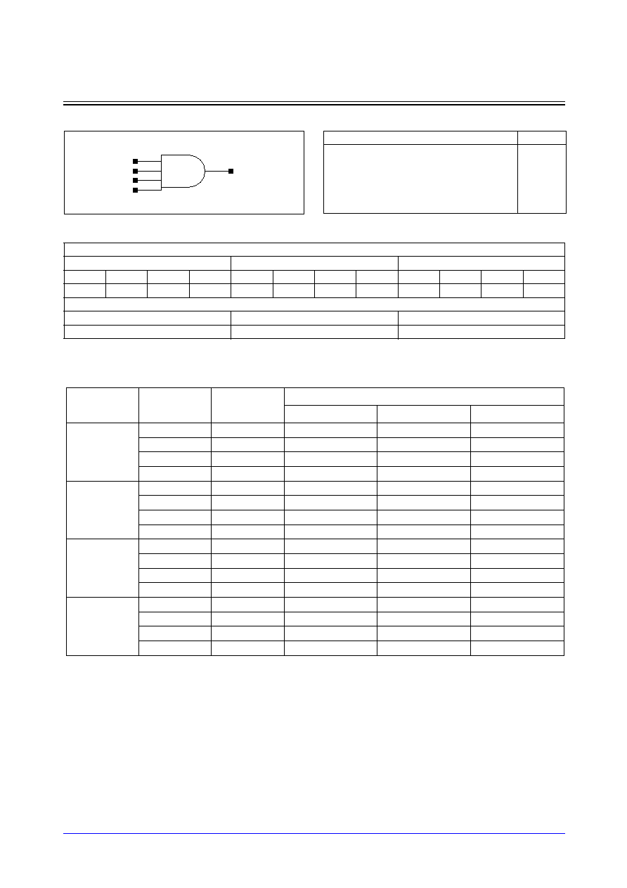
STDL131
3-20
Samsung ASIC
AD4_LP/AD4D2_LP/AD4D4_LP
4-Input AND with 1X/2X/4X Drive
Logic Symbol
Cell Data
Switching Characteristics
(Typical process, 25
∞
C, 1.8V, t
R
/t
F
= 0.19ns, SL: Standard Load)
AD4_LP
Input Load (SL)
AD4_LP
AD4D2_LP
AD4D4_LP
A
B
C
D
A
B
C
D
A
B
C
D
0.8
0.8
0.8
0.8
0.9
0.9
1.0
0.9
0.9
0.9
0.9
0.9
Gate Count
AD4_LP
AD4D2_LP
AD4D4_LP
2.33
2.33
3.00
A
B
C
Y
D
Path
Parameter
Delay [ns]
SL = 2
Delay Equations [ns]
Group1*
Group2*
Group3*
A to Y
tR
0.121
0.070 + 0.026*SL
0.071 + 0.025*SL
0.067 + 0.026*SL
tF
0.081
0.048 + 0.016*SL
0.048 + 0.016*SL
0.046 + 0.017*SL
tPLH
0.210
0.176 + 0.017*SL
0.188 + 0.014*SL
0.196 + 0.013*SL
tPHL
0.192
0.167 + 0.013*SL
0.176 + 0.011*SL
0.182 + 0.010*SL
B to Y
tR
0.121
0.071 + 0.025*SL
0.071 + 0.025*SL
0.067 + 0.026*SL
tF
0.083
0.050 + 0.016*SL
0.050 + 0.016*SL
0.049 + 0.016*SL
tPLH
0.221
0.187 + 0.017*SL
0.199 + 0.014*SL
0.208 + 0.013*SL
tPHL
0.207
0.181 + 0.013*SL
0.190 + 0.011*SL
0.197 + 0.010*SL
C to Y
tR
0.121
0.070 + 0.025*SL
0.071 + 0.025*SL
0.066 + 0.026*SL
tF
0.084
0.050 + 0.017*SL
0.055 + 0.016*SL
0.050 + 0.017*SL
tPLH
0.228
0.194 + 0.017*SL
0.206 + 0.014*SL
0.214 + 0.013*SL
tPHL
0.219
0.192 + 0.013*SL
0.202 + 0.011*SL
0.210 + 0.010*SL
D to Y
tR
0.121
0.071 + 0.025*SL
0.071 + 0.025*SL
0.066 + 0.026*SL
tF
0.087
0.055 + 0.016*SL
0.054 + 0.016*SL
0.053 + 0.016*SL
tPLH
0.231
0.197 + 0.017*SL
0.209 + 0.014*SL
0.218 + 0.013*SL
tPHL
0.229
0.202 + 0.013*SL
0.212 + 0.011*SL
0.220 + 0.010*SL
*Group1 : SL < 4, *Group2 : 4 SL
<
<
=
= 8, *Group3 : 8 < SL
Truth Table
A
B
C
D
Y
0
x
x
x
0
x
0
x
x
0
x
x
0
x
0
x
x
x
0
0
1
1
1
1
1

Samsung ASIC
3-21
STDL131
AD4_LP/AD4D2_LP/AD4D4_LP
4-Input AND with 1X/2X/4X Drive
Switching Characteristics
(Typical process, 25
∞
C, 1.8V, t
R
/t
F
= 0.19ns, SL: Standard Load)
AD4D2_LP
AD4D4_LP
Path
Parameter
Delay [ns]
SL = 2
Delay Equations [ns]
Group1*
Group2*
Group3*
A to Y
tR
0.097
0.069 + 0.014*SL
0.074 + 0.013*SL
0.075 + 0.013*SL
tF
0.063
0.045 + 0.009*SL
0.047 + 0.009*SL
0.049 + 0.008*SL
tPLH
0.217
0.194 + 0.011*SL
0.206 + 0.008*SL
0.224 + 0.007*SL
tPHL
0.187
0.170 + 0.008*SL
0.179 + 0.006*SL
0.191 + 0.005*SL
B to Y
tR
0.097
0.068 + 0.014*SL
0.074 + 0.013*SL
0.074 + 0.013*SL
tF
0.065
0.047 + 0.009*SL
0.049 + 0.008*SL
0.050 + 0.008*SL
tPLH
0.227
0.204 + 0.011*SL
0.216 + 0.008*SL
0.234 + 0.007*SL
tPHL
0.199
0.182 + 0.008*SL
0.191 + 0.006*SL
0.203 + 0.005*SL
C to Y
tR
0.096
0.067 + 0.015*SL
0.075 + 0.013*SL
0.074 + 0.013*SL
tF
0.067
0.047 + 0.010*SL
0.054 + 0.008*SL
0.051 + 0.008*SL
tPLH
0.232
0.210 + 0.011*SL
0.222 + 0.008*SL
0.240 + 0.007*SL
tPHL
0.208
0.191 + 0.009*SL
0.201 + 0.006*SL
0.214 + 0.005*SL
D to Y
tR
0.095
0.064 + 0.015*SL
0.075 + 0.013*SL
0.074 + 0.013*SL
tF
0.068
0.049 + 0.009*SL
0.053 + 0.008*SL
0.055 + 0.008*SL
tPLH
0.236
0.214 + 0.011*SL
0.226 + 0.008*SL
0.244 + 0.007*SL
tPHL
0.217
0.199 + 0.009*SL
0.209 + 0.006*SL
0.223 + 0.005*SL
*Group1 : SL < 4, *Group2 : 4 SL
<
<
=
= 12, *Group3 : 12 < SL
Path
Parameter
Delay [ns]
SL = 2
Delay Equations [ns]
Group1*
Group2*
Group3*
A to Y
tR
0.101
0.083 + 0.009*SL
0.091 + 0.007*SL
0.104 + 0.006*SL
tF
0.072
0.059 + 0.006*SL
0.067 + 0.004*SL
0.075 + 0.004*SL
tPLH
0.269
0.254 + 0.007*SL
0.263 + 0.005*SL
0.292 + 0.004*SL
tPHL
0.233
0.221 + 0.006*SL
0.229 + 0.004*SL
0.252 + 0.003*SL
B to Y
tR
0.102
0.084 + 0.009*SL
0.092 + 0.007*SL
0.104 + 0.006*SL
tF
0.075
0.063 + 0.006*SL
0.069 + 0.004*SL
0.077 + 0.004*SL
tPLH
0.280
0.265 + 0.007*SL
0.274 + 0.005*SL
0.303 + 0.004*SL
tPHL
0.246
0.234 + 0.006*SL
0.242 + 0.004*SL
0.265 + 0.003*SL
C to Y
tR
0.102
0.084 + 0.009*SL
0.092 + 0.007*SL
0.104 + 0.006*SL
tF
0.076
0.063 + 0.006*SL
0.072 + 0.004*SL
0.078 + 0.004*SL
tPLH
0.286
0.271 + 0.007*SL
0.280 + 0.005*SL
0.309 + 0.004*SL
tPHL
0.257
0.244 + 0.006*SL
0.253 + 0.004*SL
0.276 + 0.003*SL
D to Y
tR
0.102
0.085 + 0.009*SL
0.091 + 0.007*SL
0.105 + 0.006*SL
tF
0.079
0.067 + 0.006*SL
0.074 + 0.004*SL
0.082 + 0.004*SL
tPLH
0.289
0.275 + 0.007*SL
0.284 + 0.005*SL
0.313 + 0.004*SL
tPHL
0.266
0.254 + 0.006*SL
0.263 + 0.004*SL
0.286 + 0.003*SL
*Group1 : SL < 4, *Group2 : 4 SL
<
<
=
= 20, *Group3 : 20 < SL
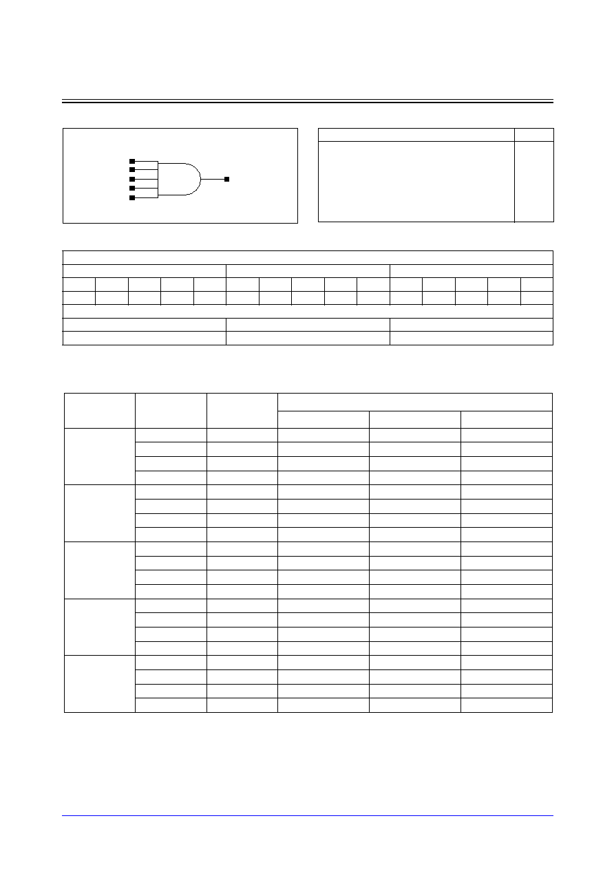
STDL131
3-22
Samsung ASIC
AD5_LP/AD5D2_LP/AD5D4_LP
5-Input AND with 1X/2X/4XDrive
Logic Symbol
Cell Data
Switching Characteristics
(Typical process, 25
∞
C, 1.8V, t
R
/t
F
= 0.19ns, SL: Standard Load)
AD5_LP
Input Load (SL)
AD5_LP
AD5D2_LP
AD5D4_LP
A
B
C
D
E
A
B
C
D
E
A
B
C
D
E
0.9
0.9
0.9
0.9
0.9
0.9
1.0
0.9
1.0
1.0
0.8
0.8
0.8
0.8
0.8
Gate Count
AD5_LP
AD5D2_LP
AD5D4_LP
3.33
3.33
5.00
B
C
D
Y
E
A
Path
Parameter
Delay [ns]
SL = 2
Delay Equations [ns]
Group1*
Group2*
Group3*
A to Y
tR
0.206
0.103 + 0.051*SL
0.099 + 0.053*SL
0.094 + 0.053*SL
tF
0.077
0.046 + 0.015*SL
0.048 + 0.015*SL
0.044 + 0.015*SL
tPLH
0.221
0.167 + 0.027*SL
0.170 + 0.026*SL
0.172 + 0.026*SL
tPHL
0.183
0.160 + 0.011*SL
0.167 + 0.010*SL
0.173 + 0.009*SL
B to Y
tR
0.206
0.104 + 0.051*SL
0.098 + 0.053*SL
0.094 + 0.053*SL
tF
0.078
0.047 + 0.015*SL
0.049 + 0.015*SL
0.047 + 0.015*SL
tPLH
0.225
0.171 + 0.027*SL
0.174 + 0.026*SL
0.176 + 0.026*SL
tPHL
0.197
0.174 + 0.011*SL
0.181 + 0.010*SL
0.187 + 0.009*SL
C to Y
tR
0.206
0.103 + 0.052*SL
0.098 + 0.053*SL
0.094 + 0.053*SL
tF
0.080
0.051 + 0.015*SL
0.051 + 0.015*SL
0.047 + 0.015*SL
tPLH
0.226
0.172 + 0.027*SL
0.175 + 0.026*SL
0.177 + 0.026*SL
tPHL
0.208
0.184 + 0.012*SL
0.192 + 0.010*SL
0.198 + 0.009*SL
D to Y
tR
0.200
0.094 + 0.053*SL
0.093 + 0.053*SL
0.091 + 0.053*SL
tF
0.087
0.057 + 0.015*SL
0.057 + 0.015*SL
0.052 + 0.015*SL
tPLH
0.216
0.163 + 0.026*SL
0.164 + 0.026*SL
0.165 + 0.026*SL
tPHL
0.181
0.160 + 0.011*SL
0.165 + 0.009*SL
0.168 + 0.009*SL
E to Y
tR
0.199
0.093 + 0.053*SL
0.092 + 0.053*SL
0.091 + 0.053*SL
tF
0.087
0.057 + 0.015*SL
0.055 + 0.015*SL
0.054 + 0.015*SL
tPLH
0.214
0.161 + 0.026*SL
0.163 + 0.026*SL
0.164 + 0.026*SL
tPHL
0.195
0.174 + 0.011*SL
0.179 + 0.009*SL
0.183 + 0.009*SL
*Group1 : SL < 4, *Group2 : 4 SL
<
<
=
= 8, *Group3 : 8 < SL
Truth Table
A
B
C
D
E
Y
0
x
x
x
x
0
x
0
x
x
x
0
x
x
0
x
x
0
x
x
x
0
x
0
x
x
x
x
0
0
1
1
1
1
1
1

Samsung ASIC
3-23
STDL131
AD5_LP/AD5D2_LP/AD5D4_LP
5-Input AND with 1X/2X/4X Drive
Switching Characteristics
(Typical process, 25
∞
C, 1.8V, t
R
/t
F
= 0.19ns, SL: Standard Load)
AD5D2_LP
Path
Parameter
Delay [ns]
SL = 2
Delay Equations [ns]
Group1*
Group2*
Group3*
A to Y
tR
0.149
0.097 + 0.026*SL
0.096 + 0.026*SL
0.088 + 0.027*SL
tF
0.064
0.046 + 0.009*SL
0.050 + 0.008*SL
0.050 + 0.008*SL
tPLH
0.218
0.188 + 0.015*SL
0.194 + 0.014*SL
0.198 + 0.013*SL
tPHL
0.186
0.171 + 0.007*SL
0.178 + 0.006*SL
0.190 + 0.005*SL
B to Y
tR
0.149
0.098 + 0.026*SL
0.096 + 0.026*SL
0.088 + 0.027*SL
tF
0.065
0.050 + 0.008*SL
0.050 + 0.008*SL
0.051 + 0.008*SL
tPLH
0.221
0.191 + 0.015*SL
0.197 + 0.014*SL
0.201 + 0.013*SL
tPHL
0.198
0.183 + 0.007*SL
0.190 + 0.006*SL
0.201 + 0.005*SL
C to Y
tR
0.149
0.097 + 0.026*SL
0.096 + 0.026*SL
0.088 + 0.027*SL
tF
0.067
0.050 + 0.009*SL
0.055 + 0.007*SL
0.053 + 0.008*SL
tPLH
0.220
0.190 + 0.015*SL
0.196 + 0.014*SL
0.200 + 0.013*SL
tPHL
0.207
0.192 + 0.008*SL
0.200 + 0.006*SL
0.211 + 0.005*SL
D to Y
tR
0.143
0.092 + 0.025*SL
0.088 + 0.027*SL
0.083 + 0.027*SL
tF
0.072
0.056 + 0.008*SL
0.059 + 0.008*SL
0.056 + 0.008*SL
tPLH
0.211
0.182 + 0.015*SL
0.187 + 0.013*SL
0.190 + 0.013*SL
tPHL
0.183
0.170 + 0.006*SL
0.175 + 0.005*SL
0.183 + 0.005*SL
E to Y
tR
0.138
0.084 + 0.027*SL
0.084 + 0.027*SL
0.082 + 0.027*SL
tF
0.074
0.059 + 0.008*SL
0.058 + 0.008*SL
0.057 + 0.008*SL
tPLH
0.210
0.181 + 0.014*SL
0.185 + 0.013*SL
0.188 + 0.013*SL
tPHL
0.195
0.182 + 0.006*SL
0.186 + 0.005*SL
0.194 + 0.005*SL
*Group1 : SL < 4, *Group2 : 4 SL
<
<
=
= 12, *Group3 : 12 < SL

STDL131
3-24
Samsung ASIC
AD5_LP/AD5D2_LP/AD5D4_LP
5-Input AND with 1X/2X/4X Drive
Switching Characteristics
(Typical process, 25
∞
C, 1.8V, t
R
/t
F
= 0.19ns, SL: Standard Load)
AD5D4_LP
Path
Parameter
Delay [ns]
SL = 2
Delay Equations [ns]
Group1*
Group2*
Group3*
A to Y
tR
0.063
0.051 + 0.006*SL
0.050 + 0.006*SL
0.042 + 0.006*SL
tF
0.054
0.044 + 0.005*SL
0.047 + 0.004*SL
0.047 + 0.004*SL
tPLH
0.342
0.332 + 0.005*SL
0.337 + 0.004*SL
0.345 + 0.003*SL
tPHL
0.313
0.304 + 0.005*SL
0.310 + 0.003*SL
0.324 + 0.003*SL
B to Y
tR
0.063
0.050 + 0.006*SL
0.051 + 0.006*SL
0.043 + 0.006*SL
tF
0.055
0.044 + 0.005*SL
0.049 + 0.004*SL
0.049 + 0.004*SL
tPLH
0.345
0.335 + 0.005*SL
0.341 + 0.004*SL
0.349 + 0.003*SL
tPHL
0.328
0.319 + 0.005*SL
0.325 + 0.003*SL
0.339 + 0.003*SL
C to Y
tR
0.062
0.049 + 0.007*SL
0.052 + 0.006*SL
0.043 + 0.006*SL
tF
0.055
0.047 + 0.004*SL
0.046 + 0.004*SL
0.048 + 0.004*SL
tPLH
0.345
0.336 + 0.005*SL
0.341 + 0.004*SL
0.349 + 0.003*SL
tPHL
0.341
0.332 + 0.005*SL
0.338 + 0.003*SL
0.352 + 0.003*SL
D to Y
tR
0.063
0.050 + 0.007*SL
0.052 + 0.006*SL
0.043 + 0.006*SL
tF
0.055
0.044 + 0.005*SL
0.049 + 0.004*SL
0.049 + 0.004*SL
tPLH
0.340
0.330 + 0.005*SL
0.336 + 0.004*SL
0.344 + 0.003*SL
tPHL
0.315
0.306 + 0.005*SL
0.312 + 0.003*SL
0.326 + 0.003*SL
E to Y
tR
0.063
0.049 + 0.007*SL
0.052 + 0.006*SL
0.043 + 0.006*SL
tF
0.055
0.045 + 0.005*SL
0.048 + 0.004*SL
0.047 + 0.004*SL
tPLH
0.339
0.329 + 0.005*SL
0.335 + 0.004*SL
0.343 + 0.003*SL
tPHL
0.332
0.323 + 0.005*SL
0.329 + 0.003*SL
0.343 + 0.003*SL
*Group1 : SL < 4, *Group2 : 4 SL
<
<
=
= 20, *Group3 : 20 < SL
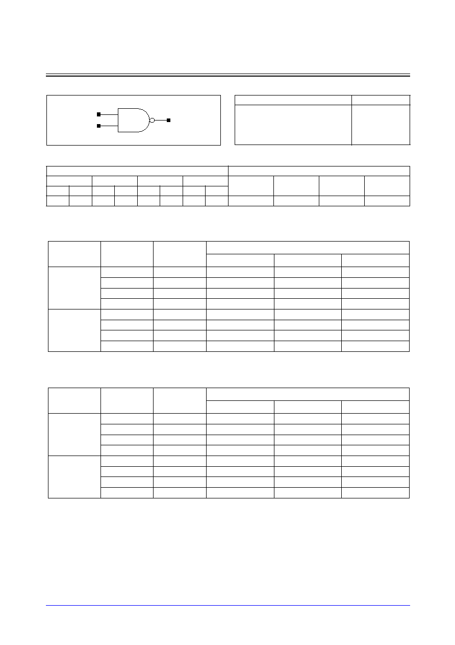
Samsung ASIC
3-25
STDL131
ND2_LP/ND2D2_LP/ND2D4_LP/ND2D8_LP
2-Input NAND with 1X/2X/4X/8X Drive
Logic Symbol
Cell Data
Switching Characteristics
(Typical process, 25
∞
C, 1.8V, t
R
/t
F
= 0.19ns, SL: Standard Load)
ND2_LP
ND2D2_LP
Input Load (SL)
Gate Count
ND2_LP
ND2D2_LP ND2D4_LP ND2D8_LP
ND2_LP
ND2D2_LP ND2D4_LP ND2D8_LP
A
B
A
B
A
B
A
B
1.1
1.1
2.3
2.2
4.5
4.5
1.1
1.1
1.00
1.67
3.00
4.33
A
B
Y
Path
Parameter
Delay [ns]
SL = 2
Delay Equations [ns]
Group1*
Group2*
Group3*
A to Y
tR
0.122
0.079 + 0.022*SL
0.068 + 0.024*SL
0.056 + 0.026*SL
tF
0.120
0.076 + 0.022*SL
0.067 + 0.024*SL
0.058 + 0.025*SL
tPLH
0.102
0.074 + 0.014*SL
0.080 + 0.013*SL
0.081 + 0.013*SL
tPHL
0.094
0.062 + 0.016*SL
0.070 + 0.014*SL
0.070 + 0.014*SL
B to Y
tR
0.128
0.083 + 0.022*SL
0.073 + 0.025*SL
0.064 + 0.026*SL
tF
0.111
0.064 + 0.024*SL
0.058 + 0.025*SL
0.052 + 0.026*SL
tPLH
0.111
0.084 + 0.013*SL
0.088 + 0.013*SL
0.088 + 0.013*SL
tPHL
0.090
0.059 + 0.016*SL
0.066 + 0.014*SL
0.067 + 0.014*SL
*Group1 : SL < 4, *Group2 : 4 SL
<
<
=
= 8, *Group3 : 8 < SL
Path
Parameter
Delay [ns]
SL = 2
Delay Equations [ns]
Group1*
Group2*
Group3*
A to Y
tR
0.099
0.078 + 0.011*SL
0.074 + 0.012*SL
0.061 + 0.013*SL
tF
0.098
0.077 + 0.011*SL
0.073 + 0.012*SL
0.061 + 0.013*SL
tPLH
0.087
0.070 + 0.009*SL
0.079 + 0.006*SL
0.081 + 0.006*SL
tPHL
0.077
0.058 + 0.010*SL
0.067 + 0.007*SL
0.070 + 0.007*SL
B to Y
tR
0.106
0.085 + 0.010*SL
0.080 + 0.012*SL
0.067 + 0.013*SL
tF
0.088
0.065 + 0.011*SL
0.062 + 0.012*SL
0.053 + 0.013*SL
tPLH
0.097
0.081 + 0.008*SL
0.087 + 0.006*SL
0.088 + 0.006*SL
tPHL
0.075
0.057 + 0.009*SL
0.063 + 0.007*SL
0.067 + 0.007*SL
*Group1 : SL < 4, *Group2 : 4 SL
<
<
=
= 12, *Group3 : 12 < SL
Truth Table
A
B
Y
0
0
1
0
1
1
1
0
1
1
1
0

STDL131
3-26
Samsung ASIC
ND2_LP/ND2D2_LP/ND2D4_LP/ND2D8_LP
2-Input NAND with 1X/2X/4X/8X Drive
Switching Characteristics
(Typical process, 25
∞
C, 1.8V, t
R
/t
F
= 0.19ns, SL: Standard Load)
ND2D4_LP
ND2D8_LP
Path
Parameter
Delay [ns]
SL = 2
Delay Equations [ns]
Group1*
Group2*
Group3*
A to Y
tR
0.088
0.075 + 0.006*SL
0.078 + 0.006*SL
0.061 + 0.006*SL
tF
0.086
0.074 + 0.006*SL
0.075 + 0.006*SL
0.061 + 0.006*SL
tPLH
0.077
0.067 + 0.005*SL
0.073 + 0.003*SL
0.080 + 0.003*SL
tPHL
0.066
0.055 + 0.005*SL
0.061 + 0.004*SL
0.070 + 0.003*SL
B to Y
tR
0.093
0.083 + 0.005*SL
0.081 + 0.006*SL
0.069 + 0.006*SL
tF
0.075
0.064 + 0.006*SL
0.062 + 0.006*SL
0.054 + 0.006*SL
tPLH
0.088
0.079 + 0.004*SL
0.084 + 0.003*SL
0.087 + 0.003*SL
tPHL
0.065
0.055 + 0.005*SL
0.059 + 0.004*SL
0.066 + 0.004*SL
*Group1 : SL < 4, *Group2 : 4 SL
<
<
=
= 20, *Group3 : 20 < SL
Path
Parameter
Delay [ns]
SL = 2
Delay Equations [ns]
Group1*
Group2*
Group3*
A to Y
tR
0.054
0.048 + 0.003*SL
0.047 + 0.003*SL
0.040 + 0.003*SL
tF
0.050
0.046 + 0.002*SL
0.046 + 0.002*SL
0.046 + 0.002*SL
tPLH
0.233
0.228 + 0.003*SL
0.231 + 0.002*SL
0.240 + 0.002*SL
tPHL
0.243
0.238 + 0.003*SL
0.241 + 0.002*SL
0.257 + 0.001*SL
B to Y
tR
0.055
0.049 + 0.003*SL
0.049 + 0.003*SL
0.040 + 0.003*SL
tF
0.049
0.043 + 0.003*SL
0.047 + 0.002*SL
0.046 + 0.002*SL
tPLH
0.242
0.237 + 0.003*SL
0.240 + 0.002*SL
0.249 + 0.002*SL
tPHL
0.239
0.234 + 0.003*SL
0.237 + 0.002*SL
0.253 + 0.001*SL
*Group1 : SL < 4, *Group2 : 4 SL
<
<
=
= 37, *Group3 : 37 < SL
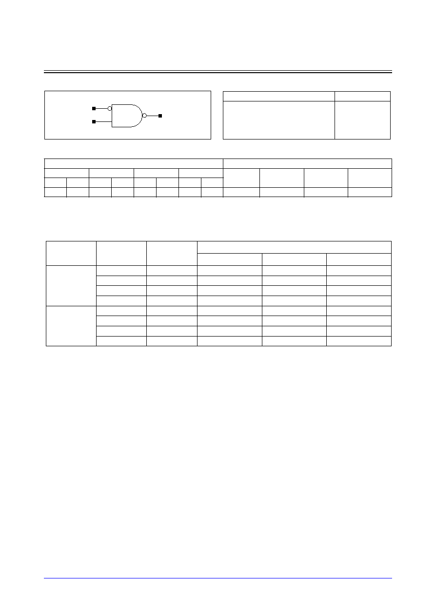
Samsung ASIC
3-27
STDL131
ND2B_LP/ND2BD2_LP/NDBD4_LP/ND2BD8_LP
2-Input NAND with one Inverted Input, 1X/2X/4X/8X Drive
Logic Symbol
Cell Data
Switching Characteristics
(Typical process, 25
∞
C, 1.8V, t
R
/t
F
= 0.19ns, SL: Standard Load)
ND2B_LP
Input Load (SL)
Gate Count
ND2B_LP
ND2BD2_LP ND2BD4_LP ND2BD8_LP ND2B_LP ND2BD2_LP ND2BD4_LP ND2BD8_LP
AN
B
AN
B
AN
B
AN
B
0.8
1.1
0.9
2.3
1.0
4.6
0.9
1.1
1.33
2.00
3.33
5.00
Truth Table
AN
B
Y
0
0
1
0
1
0
1
0
1
1
1
1
AN
B
Y
Path
Parameter
Delay [ns]
SL = 2
Delay Equations [ns]
Group1*
Group2*
Group3*
AN to Y
tR
0.104
0.053 + 0.026*SL
0.051 + 0.026*SL
0.046 + 0.027*SL
tF
0.105
0.054 + 0.026*SL
0.051 + 0.026*SL
0.048 + 0.027*SL
tPLH
0.167
0.140 + 0.013*SL
0.142 + 0.013*SL
0.144 + 0.013*SL
tPHL
0.171
0.141 + 0.015*SL
0.144 + 0.014*SL
0.146 + 0.014*SL
B to Y
tR
0.128
0.083 + 0.022*SL
0.073 + 0.025*SL
0.064 + 0.026*SL
tF
0.114
0.064 + 0.025*SL
0.061 + 0.026*SL
0.053 + 0.027*SL
tPLH
0.110
0.083 + 0.014*SL
0.087 + 0.013*SL
0.087 + 0.013*SL
tPHL
0.092
0.060 + 0.016*SL
0.067 + 0.014*SL
0.069 + 0.014*SL
*Group1 : SL < 4, *Group2 : 4 SL
<
<
=
= 8, *Group3 : 8 < SL
STDL131
3-28
Samsung ASIC
ND2B_LP/ND2BD2_LP/ND2BD4_LP/ND2BD8_LP
2-Input NAND with one Inverted Input, 1X/2X/4X/8X Drive
Switching Characteristics
(Typical process, 25
∞
C, 1.8V, t
R
/t
F
= 0.19ns, SL: Standard Load)
ND2BD2_LP
ND2BD4_LP
ND2BD8_LP
Path
Parameter
Delay [ns]
SL = 2
Delay Equations [ns]
Group1*
Group2*
Group3*
AN to Y
tR
0.084
0.060 + 0.012*SL
0.058 + 0.012*SL
0.050 + 0.013*SL
tF
0.083
0.058 + 0.013*SL
0.057 + 0.013*SL
0.051 + 0.013*SL
tPLH
0.166
0.151 + 0.008*SL
0.155 + 0.007*SL
0.158 + 0.006*SL
tPHL
0.173
0.156 + 0.008*SL
0.160 + 0.007*SL
0.164 + 0.007*SL
B to Y
tR
0.104
0.083 + 0.010*SL
0.078 + 0.012*SL
0.065 + 0.013*SL
tF
0.088
0.063 + 0.012*SL
0.062 + 0.013*SL
0.055 + 0.013*SL
tPLH
0.094
0.078 + 0.008*SL
0.084 + 0.006*SL
0.086 + 0.006*SL
tPHL
0.074
0.056 + 0.009*SL
0.062 + 0.008*SL
0.068 + 0.007*SL
*Group1 : SL < 4, *Group2 : 4 SL
<
<
=
= 12, *Group3 : 12 < SL
Path
Parameter
Delay [ns]
SL = 2
Delay Equations [ns]
Group1*
Group2*
Group3*
AN to Y
tR
0.081
0.068 + 0.006*SL
0.069 + 0.006*SL
0.061 + 0.006*SL
tF
0.079
0.067 + 0.006*SL
0.067 + 0.006*SL
0.062 + 0.007*SL
tPLH
0.186
0.177 + 0.005*SL
0.180 + 0.004*SL
0.189 + 0.003*SL
tPHL
0.196
0.186 + 0.005*SL
0.190 + 0.004*SL
0.199 + 0.004*SL
B to Y
tR
0.092
0.081 + 0.006*SL
0.080 + 0.006*SL
0.068 + 0.006*SL
tF
0.074
0.060 + 0.007*SL
0.062 + 0.006*SL
0.057 + 0.007*SL
tPLH
0.085
0.076 + 0.005*SL
0.081 + 0.003*SL
0.085 + 0.003*SL
tPHL
0.065
0.055 + 0.005*SL
0.059 + 0.004*SL
0.068 + 0.004*SL
*Group1 : SL < 4, *Group2 : 4 SL
<
<
=
= 20, *Group3 : 20 < SL
Path
Parameter
Delay [ns]
SL = 2
Delay Equations [ns]
Group1*
Group2*
Group3*
AN to Y
tR
0.052
0.046 + 0.003*SL
0.047 + 0.003*SL
0.040 + 0.003*SL
tF
0.049
0.045 + 0.002*SL
0.045 + 0.002*SL
0.048 + 0.002*SL
tPLH
0.284
0.279 + 0.003*SL
0.282 + 0.002*SL
0.291 + 0.002*SL
tPHL
0.313
0.308 + 0.003*SL
0.312 + 0.002*SL
0.327 + 0.001*SL
B to Y
tR
0.055
0.048 + 0.003*SL
0.049 + 0.003*SL
0.040 + 0.003*SL
tF
0.050
0.045 + 0.002*SL
0.046 + 0.002*SL
0.047 + 0.002*SL
tPLH
0.241
0.236 + 0.003*SL
0.239 + 0.002*SL
0.249 + 0.002*SL
tPHL
0.242
0.237 + 0.003*SL
0.241 + 0.002*SL
0.256 + 0.001*SL
*Group1 : SL < 4, *Group2 : 4 SL
<
<
=
= 37, *Group3 : 37 < SL
Samsung ASIC
3-29
STDL131
ND3_LP/ND3D2_LP/ND3D4_LP/ND3D8_LP
3-Input NAND with 1X/2X/4X/8X Drive
Logic Symbol
Cell Data
Input Load (SL)
ND3_LP
ND3D2_LP
ND3D4_LP
ND3D8_LP
A
B
C
A
B
C
A
B
C
A
B
C
0.9
0.9
0.9
2.0
1.9
1.9
0.5
0.5
0.6
0.9
0.9
1.0
Gate Count
ND3_LP
ND3D2_LP
ND3D4_LP
ND3D8_LP
1.33
2.33
3.33
5.00
A
B
C
Y
Truth Table
A
B
C
Y
0
x
x
1
x
0
x
1
x
x
0
1
1
1
1
0

STDL131
3-30
Samsung ASIC
ND3_LP/ND3D2_LP/ND3D4_LP/ND3D8_LP
3-Input NAND with 1X/2X/4X/8X Drive
Switching Characteristics
(Typical process, 25
∞
C, 1.8V, t
R
/t
F
= 0.19ns, SL: Standard Load)
ND3_LP
ND3D2_LP
Path
Parameter
Delay [ns]
SL = 2
Delay Equations [ns]
Group1*
Group2*
Group3*
A to Y
tR
0.155
0.091 + 0.032*SL
0.081 + 0.035*SL
0.070 + 0.036*SL
tF
0.164
0.096 + 0.034*SL
0.088 + 0.036*SL
0.079 + 0.037*SL
tPLH
0.125
0.090 + 0.017*SL
0.091 + 0.017*SL
0.092 + 0.017*SL
tPHL
0.118
0.077 + 0.020*SL
0.080 + 0.020*SL
0.080 + 0.020*SL
B to Y
tR
0.163
0.097 + 0.033*SL
0.091 + 0.035*SL
0.080 + 0.036*SL
tF
0.158
0.086 + 0.036*SL
0.082 + 0.037*SL
0.077 + 0.038*SL
tPLH
0.135
0.101 + 0.017*SL
0.101 + 0.017*SL
0.102 + 0.017*SL
tPHL
0.120
0.080 + 0.020*SL
0.082 + 0.020*SL
0.083 + 0.020*SL
C to Y
tR
0.174
0.108 + 0.033*SL
0.101 + 0.035*SL
0.092 + 0.036*SL
tF
0.154
0.081 + 0.036*SL
0.078 + 0.037*SL
0.075 + 0.038*SL
tPLH
0.144
0.109 + 0.018*SL
0.110 + 0.017*SL
0.111 + 0.017*SL
tPHL
0.120
0.080 + 0.020*SL
0.082 + 0.020*SL
0.083 + 0.020*SL
*Group1 : SL < 4, *Group2 : 4 SL
<
<
=
= 8, *Group3 : 8 < SL
Path
Parameter
Delay [ns]
SL = 2
Delay Equations [ns]
Group1*
Group2*
Group3*
A to Y
tR
0.121
0.091 + 0.015*SL
0.083 + 0.017*SL
0.071 + 0.018*SL
tF
0.127
0.095 + 0.016*SL
0.090 + 0.017*SL
0.078 + 0.018*SL
tPLH
0.105
0.085 + 0.010*SL
0.090 + 0.009*SL
0.090 + 0.009*SL
tPHL
0.093
0.071 + 0.011*SL
0.076 + 0.010*SL
0.077 + 0.010*SL
B to Y
tR
0.128
0.097 + 0.016*SL
0.092 + 0.017*SL
0.081 + 0.018*SL
tF
0.120
0.087 + 0.016*SL
0.082 + 0.018*SL
0.074 + 0.018*SL
tPLH
0.116
0.098 + 0.009*SL
0.100 + 0.009*SL
0.100 + 0.009*SL
tPHL
0.096
0.074 + 0.011*SL
0.079 + 0.010*SL
0.080 + 0.010*SL
C to Y
tR
0.138
0.107 + 0.016*SL
0.101 + 0.017*SL
0.091 + 0.018*SL
tF
0.114
0.079 + 0.017*SL
0.075 + 0.018*SL
0.071 + 0.018*SL
tPLH
0.124
0.107 + 0.009*SL
0.107 + 0.009*SL
0.109 + 0.009*SL
tPHL
0.096
0.075 + 0.011*SL
0.078 + 0.010*SL
0.080 + 0.010*SL
*Group1 : SL < 4, *Group2 : 4 SL
<
<
=
= 12, *Group3 : 12 < SL

Samsung ASIC
3-31
STDL131
ND3_LP/ND3D2_LP/ND3D4_LP/ND3D8_LP
3-Input NAND with 1X/2X/4X/8X Drive
Switching Characteristics
(Typical process, 25
∞
C, 1.8V, t
R
/t
F
= 0.19ns, SL: Standard Load)
ND3D4_LP
ND3D8_LP
Path
Parameter
Delay [ns]
SL = 2
Delay Equations [ns]
Group1*
Group2*
Group3*
A to Y
tR
0.062
0.048 + 0.007*SL
0.052 + 0.006*SL
0.043 + 0.006*SL
tF
0.057
0.048 + 0.005*SL
0.050 + 0.004*SL
0.051 + 0.004*SL
tPLH
0.285
0.276 + 0.005*SL
0.281 + 0.004*SL
0.289 + 0.003*SL
tPHL
0.282
0.272 + 0.005*SL
0.279 + 0.003*SL
0.293 + 0.003*SL
B to Y
tR
0.063
0.049 + 0.007*SL
0.052 + 0.006*SL
0.043 + 0.006*SL
tF
0.057
0.046 + 0.006*SL
0.051 + 0.004*SL
0.051 + 0.004*SL
tPLH
0.300
0.291 + 0.005*SL
0.296 + 0.004*SL
0.304 + 0.003*SL
tPHL
0.286
0.277 + 0.005*SL
0.283 + 0.003*SL
0.297 + 0.003*SL
C to Y
tR
0.063
0.051 + 0.006*SL
0.051 + 0.006*SL
0.043 + 0.006*SL
tF
0.057
0.047 + 0.005*SL
0.051 + 0.004*SL
0.051 + 0.004*SL
tPLH
0.314
0.305 + 0.005*SL
0.310 + 0.004*SL
0.318 + 0.003*SL
tPHL
0.287
0.277 + 0.005*SL
0.283 + 0.003*SL
0.298 + 0.003*SL
*Group1 : SL < 4, *Group2 : 4 SL
<
<
=
= 20, *Group3 : 20 < SL
Path
Parameter
Delay [ns]
SL = 2
Delay Equations [ns]
Group1*
Group2*
Group3*
A to Y
tR
0.053
0.046 + 0.004*SL
0.048 + 0.003*SL
0.041 + 0.003*SL
tF
0.051
0.046 + 0.003*SL
0.048 + 0.002*SL
0.050 + 0.002*SL
tPLH
0.266
0.260 + 0.003*SL
0.264 + 0.002*SL
0.273 + 0.002*SL
tPHL
0.281
0.276 + 0.003*SL
0.280 + 0.002*SL
0.295 + 0.001*SL
B to Y
tR
0.057
0.051 + 0.003*SL
0.051 + 0.003*SL
0.041 + 0.003*SL
tF
0.052
0.048 + 0.002*SL
0.048 + 0.002*SL
0.047 + 0.002*SL
tPLH
0.278
0.273 + 0.003*SL
0.276 + 0.002*SL
0.286 + 0.002*SL
tPHL
0.285
0.279 + 0.003*SL
0.283 + 0.002*SL
0.299 + 0.001*SL
C to Y
tR
0.054
0.047 + 0.004*SL
0.049 + 0.003*SL
0.042 + 0.003*SL
tF
0.052
0.047 + 0.002*SL
0.048 + 0.002*SL
0.048 + 0.002*SL
tPLH
0.288
0.283 + 0.003*SL
0.286 + 0.002*SL
0.296 + 0.002*SL
tPHL
0.285
0.279 + 0.003*SL
0.283 + 0.002*SL
0.299 + 0.001*SL
*Group1 : SL < 4, *Group2 : 4 SL
<
<
=
= 37, *Group3 : 37 < SL

STDL131
3-32
Samsung ASIC
ND3B_LP/ND3BD2_LP/ND3BD4_LP/ND3BD8_LP
3-Input NAND with one Inverted Input, 1X/2X/4X/8X Drive
Logic Symbol
Cell Data
Input Load (SL)
ND3B_LP
ND3BD2_LP
ND3BD4_LP
ND3BD8_LP
AN
B
C
AN
B
C
AN
B
C
AN
B
C
0.8
1.0
1.0
1.0
2.0
1.9
0.8
1.0
1.0
0.8
1.0
1.0
Gate Count
ND3B_LP
ND3BD2_LP
ND3BD4_LP
ND3BD8_LP
2.00
3.00
4.00
5.33
Truth Table
AN
B
C
Y
0
1
1
0
Other Stares
1
AN
B
C
Y

Samsung ASIC
3-33
STDL131
ND3B_LP/ND3BD2_LP/ND3BD4_LP/ND3BD8_LP
3-Input NAND with one Inverted Input, 1X/2X/4X/8X Drive
Switching Characteristics
(Typical process, 25
∞
C, 1.8V, t
R
/t
F
= 0.19ns, SL: Standard Load)
ND3B_LP
ND3BD2_LP
Path
Parameter
Delay [ns]
SL = 2
Delay Equations [ns]
Group1*
Group2*
Group3*
AN to Y
tR
0.147
0.077 + 0.035*SL
0.075 + 0.035*SL
0.072 + 0.036*SL
tF
0.156
0.084 + 0.036*SL
0.082 + 0.037*SL
0.079 + 0.037*SL
tPLH
0.183
0.149 + 0.017*SL
0.150 + 0.017*SL
0.151 + 0.017*SL
tPHL
0.189
0.150 + 0.020*SL
0.151 + 0.019*SL
0.152 + 0.019*SL
B to Y
tR
0.169
0.104 + 0.032*SL
0.097 + 0.034*SL
0.086 + 0.035*SL
tF
0.164
0.094 + 0.035*SL
0.089 + 0.036*SL
0.084 + 0.037*SL
tPLH
0.137
0.103 + 0.017*SL
0.104 + 0.017*SL
0.104 + 0.017*SL
tPHL
0.124
0.084 + 0.020*SL
0.087 + 0.019*SL
0.088 + 0.019*SL
C to Y
tR
0.179
0.114 + 0.032*SL
0.107 + 0.034*SL
0.097 + 0.035*SL
tF
0.160
0.089 + 0.036*SL
0.085 + 0.037*SL
0.082 + 0.037*SL
tPLH
0.145
0.111 + 0.017*SL
0.112 + 0.017*SL
0.113 + 0.017*SL
tPHL
0.124
0.084 + 0.020*SL
0.086 + 0.019*SL
0.088 + 0.019*SL
*Group1 : SL < 4, *Group2 : 4 SL
<
<
=
= 8, *Group3 : 8 < SL
Path
Parameter
Delay [ns]
SL = 2
Delay Equations [ns]
Group1*
Group2*
Group3*
AN to Y
tR
0.108
0.074 + 0.017*SL
0.071 + 0.018*SL
0.067 + 0.018*SL
tF
0.114
0.078 + 0.018*SL
0.077 + 0.018*SL
0.073 + 0.019*SL
tPLH
0.171
0.153 + 0.009*SL
0.155 + 0.009*SL
0.156 + 0.008*SL
tPHL
0.176
0.155 + 0.010*SL
0.157 + 0.010*SL
0.159 + 0.010*SL
B to Y
tR
0.131
0.100 + 0.015*SL
0.094 + 0.017*SL
0.083 + 0.018*SL
tF
0.122
0.088 + 0.017*SL
0.085 + 0.018*SL
0.079 + 0.018*SL
tPLH
0.116
0.098 + 0.009*SL
0.100 + 0.009*SL
0.101 + 0.008*SL
tPHL
0.098
0.076 + 0.011*SL
0.081 + 0.010*SL
0.083 + 0.010*SL
C to Y
tR
0.140
0.109 + 0.015*SL
0.104 + 0.017*SL
0.093 + 0.018*SL
tF
0.117
0.081 + 0.018*SL
0.079 + 0.018*SL
0.076 + 0.018*SL
tPLH
0.125
0.108 + 0.009*SL
0.108 + 0.009*SL
0.109 + 0.008*SL
tPHL
0.099
0.078 + 0.011*SL
0.081 + 0.010*SL
0.083 + 0.010*SL
*Group1 : SL < 4, *Group2 : 4 SL
<
<
=
= 12, *Group3 : 12 < SL

STDL131
3-34
Samsung ASIC
ND3B_LP/ND3BD2_LP/ND3BD4_LP/ND3BD8_LP
3-Input NAND with one Inverted Input, 1X/2X/4X/8X Drive
Switching Characteristics
(Typical process, 25
∞
C, 1.8V, t
R
/t
F
= 0.19ns, SL: Standard Load)
ND3BD4_LP
ND3BD8_LP
Path
Parameter
Delay [ns]
SL = 2
Delay Equations [ns]
Group1*
Group2*
Group3*
AN to Y
tR
0.061
0.050 + 0.006*SL
0.048 + 0.006*SL
0.039 + 0.007*SL
tF
0.056
0.048 + 0.004*SL
0.048 + 0.004*SL
0.050 + 0.004*SL
tPLH
0.306
0.296 + 0.005*SL
0.301 + 0.004*SL
0.309 + 0.003*SL
tPHL
0.333
0.323 + 0.005*SL
0.329 + 0.003*SL
0.343 + 0.003*SL
B to Y
tR
0.062
0.050 + 0.006*SL
0.049 + 0.006*SL
0.040 + 0.007*SL
tF
0.057
0.048 + 0.004*SL
0.048 + 0.004*SL
0.049 + 0.004*SL
tPLH
0.261
0.251 + 0.005*SL
0.256 + 0.004*SL
0.264 + 0.003*SL
tPHL
0.268
0.258 + 0.005*SL
0.264 + 0.003*SL
0.279 + 0.003*SL
C to Y
tR
0.061
0.047 + 0.007*SL
0.050 + 0.006*SL
0.041 + 0.006*SL
tF
0.057
0.048 + 0.004*SL
0.048 + 0.004*SL
0.049 + 0.004*SL
tPLH
0.271
0.261 + 0.005*SL
0.266 + 0.004*SL
0.274 + 0.003*SL
tPHL
0.268
0.258 + 0.005*SL
0.264 + 0.003*SL
0.279 + 0.003*SL
*Group1 : SL < 4, *Group2 : 4 SL
<
<
=
= 20, *Group3 : 20 < SL
Path
Parameter
Delay [ns]
SL = 2
Delay Equations [ns]
Group1*
Group2*
Group3*
AN to Y
tR
0.056
0.051 + 0.003*SL
0.050 + 0.003*SL
0.041 + 0.003*SL
tF
0.052
0.048 + 0.002*SL
0.048 + 0.002*SL
0.048 + 0.002*SL
tPLH
0.320
0.315 + 0.003*SL
0.318 + 0.002*SL
0.328 + 0.002*SL
tPHL
0.348
0.343 + 0.003*SL
0.347 + 0.002*SL
0.363 + 0.001*SL
B to Y
tR
0.057
0.050 + 0.003*SL
0.051 + 0.003*SL
0.041 + 0.003*SL
tF
0.053
0.048 + 0.002*SL
0.049 + 0.002*SL
0.048 + 0.002*SL
tPLH
0.278
0.272 + 0.003*SL
0.276 + 0.002*SL
0.285 + 0.002*SL
tPHL
0.285
0.280 + 0.003*SL
0.284 + 0.002*SL
0.300 + 0.001*SL
C to Y
tR
0.054
0.047 + 0.004*SL
0.049 + 0.003*SL
0.042 + 0.003*SL
tF
0.053
0.048 + 0.002*SL
0.049 + 0.002*SL
0.047 + 0.002*SL
tPLH
0.288
0.283 + 0.003*SL
0.286 + 0.002*SL
0.296 + 0.002*SL
tPHL
0.285
0.280 + 0.003*SL
0.284 + 0.002*SL
0.300 + 0.001*SL
*Group1 : SL < 4, *Group2 : 4 SL
<
<
=
= 37, *Group3 : 37 < SL

Samsung ASIC
3-35
STDL131
ND4_LP/ND4D2_LP/ND4D4_LP
4-Input NAND with 1X/2X/4X Drive
Logic Symbol
Cell Data
Switching Characteristics
(Typical process, 25
∞
C, 1.8V, t
R
/t
F
= 0.19ns, SL: Standard Load)
ND4_LP
Input Load (SL)
ND4_LP
ND4D2_LP
ND4D4_LP
A
B
C
D
A
B
C
D
A
B
C
D
0.8
0.8
0.9
0.8
1.7
1.7
1.7
1.6
0.8
0.8
0.8
0.8
Gate Count
ND4_LP
ND4D2_LP
ND4D4_LP
1.67
3.00
3.33
A
B
C
Y
D
Path
Parameter
Delay [ns]
SL = 2
Delay Equations [ns]
Group1*
Group2*
Group3*
A to Y
tR
0.182
0.099 + 0.042*SL
0.089 + 0.044*SL
0.078 + 0.046*SL
tF
0.202
0.112 + 0.045*SL
0.104 + 0.047*SL
0.094 + 0.048*SL
tPLH
0.141
0.098 + 0.022*SL
0.098 + 0.022*SL
0.099 + 0.021*SL
tPHL
0.131
0.081 + 0.025*SL
0.082 + 0.025*SL
0.082 + 0.025*SL
B to Y
tR
0.195
0.110 + 0.043*SL
0.102 + 0.045*SL
0.092 + 0.046*SL
tF
0.199
0.107 + 0.046*SL
0.101 + 0.048*SL
0.095 + 0.048*SL
tPLH
0.154
0.111 + 0.022*SL
0.111 + 0.022*SL
0.112 + 0.022*SL
tPHL
0.139
0.089 + 0.025*SL
0.090 + 0.025*SL
0.091 + 0.025*SL
C to Y
tR
0.208
0.122 + 0.043*SL
0.115 + 0.045*SL
0.107 + 0.046*SL
tF
0.195
0.101 + 0.047*SL
0.098 + 0.048*SL
0.094 + 0.048*SL
tPLH
0.166
0.121 + 0.022*SL
0.123 + 0.022*SL
0.124 + 0.022*SL
tPHL
0.146
0.096 + 0.025*SL
0.097 + 0.025*SL
0.098 + 0.025*SL
D to Y
tR
0.222
0.136 + 0.043*SL
0.128 + 0.045*SL
0.122 + 0.046*SL
tF
0.193
0.098 + 0.047*SL
0.095 + 0.048*SL
0.093 + 0.048*SL
tPLH
0.174
0.129 + 0.023*SL
0.132 + 0.022*SL
0.134 + 0.022*SL
tPHL
0.148
0.098 + 0.025*SL
0.099 + 0.025*SL
0.100 + 0.025*SL
*Group1 : SL < 4, *Group2 : 4 SL
<
<
=
= 8, *Group3 : 8 < SL
Truth Table
A
B
C
D
Y
0
x
x
x
1
x
0
x
x
1
x
x
0
x
1
x
x
x
0
1
1
1
1
1
0

STDL131
3-36
Samsung ASIC
ND4_LP/ND4D2_LP/ND4D4_LP
4-Input NAND with 1X/2X/4X Drive
Switching Characteristics
(Typical process, 25
∞
C, 1.8V, t
R
/t
F
= 0.19ns, SL: Standard Load)
ND4D2_LP
ND4D4_LP
Path
Parameter
Delay [ns]
SL = 2
Delay Equations [ns]
Group1*
Group2*
Group3*
A to Y
tR
0.142
0.102 + 0.020*SL
0.096 + 0.022*SL
0.082 + 0.023*SL
tF
0.159
0.115 + 0.022*SL
0.111 + 0.023*SL
0.099 + 0.024*SL
tPLH
0.120
0.097 + 0.011*SL
0.099 + 0.011*SL
0.099 + 0.011*SL
tPHL
0.106
0.081 + 0.013*SL
0.082 + 0.012*SL
0.082 + 0.012*SL
B to Y
tR
0.154
0.113 + 0.020*SL
0.108 + 0.022*SL
0.096 + 0.023*SL
tF
0.155
0.110 + 0.022*SL
0.106 + 0.023*SL
0.099 + 0.024*SL
tPLH
0.133
0.112 + 0.011*SL
0.112 + 0.011*SL
0.113 + 0.011*SL
tPHL
0.115
0.088 + 0.013*SL
0.091 + 0.012*SL
0.092 + 0.012*SL
C to Y
tR
0.167
0.125 + 0.021*SL
0.121 + 0.022*SL
0.111 + 0.023*SL
tF
0.150
0.104 + 0.023*SL
0.101 + 0.024*SL
0.097 + 0.024*SL
tPLH
0.145
0.122 + 0.011*SL
0.123 + 0.011*SL
0.125 + 0.011*SL
tPHL
0.122
0.096 + 0.013*SL
0.098 + 0.012*SL
0.099 + 0.012*SL
D to Y
tR
0.181
0.139 + 0.021*SL
0.134 + 0.022*SL
0.125 + 0.023*SL
tF
0.147
0.100 + 0.023*SL
0.098 + 0.024*SL
0.096 + 0.024*SL
tPLH
0.153
0.130 + 0.012*SL
0.131 + 0.011*SL
0.134 + 0.011*SL
tPHL
0.124
0.098 + 0.013*SL
0.100 + 0.012*SL
0.101 + 0.012*SL
*Group1 : SL < 4, *Group2 : 4 SL
<
<
=
= 12, *Group3 : 12 < SL
Path
Parameter
Delay [ns]
SL = 2
Delay Equations [ns]
Group1*
Group2*
Group3*
A to Y
tR
0.059
0.046 + 0.006*SL
0.047 + 0.006*SL
0.039 + 0.007*SL
tF
0.057
0.049 + 0.004*SL
0.049 + 0.004*SL
0.052 + 0.004*SL
tPLH
0.266
0.256 + 0.005*SL
0.261 + 0.003*SL
0.268 + 0.003*SL
tPHL
0.279
0.269 + 0.005*SL
0.275 + 0.003*SL
0.290 + 0.003*SL
B to Y
tR
0.061
0.050 + 0.005*SL
0.047 + 0.006*SL
0.038 + 0.007*SL
tF
0.058
0.047 + 0.005*SL
0.052 + 0.004*SL
0.051 + 0.004*SL
tPLH
0.282
0.273 + 0.005*SL
0.277 + 0.003*SL
0.284 + 0.003*SL
tPHL
0.287
0.278 + 0.005*SL
0.284 + 0.003*SL
0.299 + 0.003*SL
C to Y
tR
0.060
0.046 + 0.007*SL
0.049 + 0.006*SL
0.040 + 0.007*SL
tF
0.058
0.048 + 0.005*SL
0.050 + 0.004*SL
0.052 + 0.004*SL
tPLH
0.297
0.287 + 0.005*SL
0.292 + 0.004*SL
0.300 + 0.003*SL
tPHL
0.294
0.284 + 0.005*SL
0.290 + 0.003*SL
0.305 + 0.003*SL
D to Y
tR
0.060
0.049 + 0.006*SL
0.047 + 0.006*SL
0.039 + 0.007*SL
tF
0.057
0.046 + 0.006*SL
0.052 + 0.004*SL
0.052 + 0.004*SL
tPLH
0.309
0.300 + 0.005*SL
0.305 + 0.003*SL
0.312 + 0.003*SL
tPHL
0.296
0.287 + 0.005*SL
0.293 + 0.003*SL
0.307 + 0.003*SL
*Group1 : SL < 4, *Group2 : 4 SL
<
<
=
= 20, *Group3 : 20 < SL
Samsung ASIC
3-37
STDL131
ND5_LP/ND5D2_LP/ND5D4_LP
5-Input NAND with 1X/2X/4X Drive
Logic Symbol
Cell Data
Switching Characteristics
(Typical process, 25
∞
C, 1.8V, t
R
/t
F
= 0.19ns, SL: Standard Load)
ND5_LP
Input Load (SL)
ND5_LP
ND5D2_LP
ND5D4_LP
A
B
C
D
E
A
B
C
D
E
A
B
C
D
E
0.8
0.8
0.8
0.8
0.9
0.8
0.8
0.8
0.8
0.9
0.8
0.8
0.8
0.8
0.9
Gate Count
ND5_LP
ND5D2_LP
ND5D4_LP
3.33
3.67
4.33
B
C
D
Y
E
A
Path
Parameter
Delay [ns]
SL = 2
Delay Equations [ns]
Group1*
Group2*
Group3*
A to Y
tR
0.091
0.040 + 0.025*SL
0.037 + 0.026*SL
0.032 + 0.027*SL
tF
0.085
0.051 + 0.017*SL
0.052 + 0.017*SL
0.052 + 0.017*SL
tPLH
0.248
0.221 + 0.013*SL
0.223 + 0.013*SL
0.224 + 0.013*SL
tPHL
0.262
0.234 + 0.014*SL
0.244 + 0.011*SL
0.253 + 0.010*SL
B to Y
tR
0.091
0.039 + 0.026*SL
0.037 + 0.026*SL
0.032 + 0.027*SL
tF
0.084
0.048 + 0.018*SL
0.053 + 0.017*SL
0.052 + 0.017*SL
tPLH
0.264
0.237 + 0.013*SL
0.240 + 0.013*SL
0.240 + 0.013*SL
tPHL
0.265
0.237 + 0.014*SL
0.248 + 0.011*SL
0.256 + 0.010*SL
C to Y
tR
0.090
0.039 + 0.025*SL
0.035 + 0.026*SL
0.033 + 0.027*SL
tF
0.085
0.050 + 0.017*SL
0.052 + 0.017*SL
0.052 + 0.017*SL
tPLH
0.279
0.252 + 0.013*SL
0.254 + 0.013*SL
0.256 + 0.013*SL
tPHL
0.266
0.238 + 0.014*SL
0.248 + 0.011*SL
0.257 + 0.010*SL
D to Y
tR
0.091
0.040 + 0.026*SL
0.038 + 0.026*SL
0.032 + 0.027*SL
tF
0.084
0.049 + 0.018*SL
0.052 + 0.017*SL
0.052 + 0.017*SL
tPLH
0.237
0.210 + 0.013*SL
0.213 + 0.013*SL
0.214 + 0.013*SL
tPHL
0.261
0.233 + 0.014*SL
0.243 + 0.011*SL
0.252 + 0.010*SL
E to Y
tR
0.090
0.038 + 0.026*SL
0.037 + 0.026*SL
0.033 + 0.027*SL
tF
0.085
0.049 + 0.018*SL
0.054 + 0.017*SL
0.053 + 0.017*SL
tPLH
0.252
0.225 + 0.013*SL
0.228 + 0.013*SL
0.229 + 0.013*SL
tPHL
0.259
0.232 + 0.014*SL
0.242 + 0.011*SL
0.250 + 0.010*SL
*Group1 : SL < 4, *Group2 : 4 SL
<
<
=
= 8, *Group3 : 8 < SL
Truth Table
A
B
C
D
E
Y
0
x
x
x
x
1
x
0
x
x
x
1
x
x
0
x
x
1
x
x
x
0
x
1
x
x
x
x
0
1
1
1
1
1
1
0

STDL131
3-38
Samsung ASIC
ND5_LP/ND5D2_LP/ND5D4_LP
5-Input NAND with 1X/2X/4X Drive
Switching Characteristics
(Typical process, 25
∞
C, 1.8V, t
R
/t
F
= 0.19ns, SL: Standard Load)
ND5D2_LP
Path
Parameter
Delay [ns]
SL = 2
Delay Equations [ns]
Group1*
Group2*
Group3*
A to Y
tR
0.067
0.043 + 0.012*SL
0.041 + 0.013*SL
0.034 + 0.013*SL
tF
0.072
0.052 + 0.010*SL
0.059 + 0.009*SL
0.061 + 0.008*SL
tPLH
0.262
0.247 + 0.008*SL
0.252 + 0.007*SL
0.255 + 0.006*SL
tPHL
0.270
0.252 + 0.009*SL
0.262 + 0.007*SL
0.277 + 0.005*SL
B to Y
tR
0.068
0.045 + 0.012*SL
0.041 + 0.013*SL
0.034 + 0.013*SL
tF
0.072
0.052 + 0.010*SL
0.058 + 0.009*SL
0.060 + 0.008*SL
tPLH
0.279
0.263 + 0.008*SL
0.268 + 0.007*SL
0.271 + 0.006*SL
tPHL
0.274
0.255 + 0.009*SL
0.265 + 0.007*SL
0.281 + 0.005*SL
C to Y
tR
0.069
0.046 + 0.011*SL
0.042 + 0.012*SL
0.034 + 0.013*SL
tF
0.072
0.052 + 0.010*SL
0.059 + 0.009*SL
0.061 + 0.008*SL
tPLH
0.294
0.278 + 0.008*SL
0.284 + 0.007*SL
0.287 + 0.006*SL
tPHL
0.274
0.256 + 0.009*SL
0.266 + 0.007*SL
0.281 + 0.005*SL
D to Y
tR
0.069
0.046 + 0.012*SL
0.042 + 0.013*SL
0.035 + 0.013*SL
tF
0.072
0.053 + 0.010*SL
0.058 + 0.008*SL
0.058 + 0.008*SL
tPLH
0.253
0.237 + 0.008*SL
0.242 + 0.007*SL
0.246 + 0.006*SL
tPHL
0.269
0.251 + 0.009*SL
0.260 + 0.007*SL
0.276 + 0.005*SL
E to Y
tR
0.068
0.045 + 0.012*SL
0.042 + 0.013*SL
0.035 + 0.013*SL
tF
0.072
0.051 + 0.010*SL
0.058 + 0.009*SL
0.061 + 0.008*SL
tPLH
0.268
0.252 + 0.008*SL
0.257 + 0.007*SL
0.261 + 0.006*SL
tPHL
0.267
0.249 + 0.009*SL
0.259 + 0.007*SL
0.274 + 0.005*SL
*Group1 : SL < 4, *Group2 : 4 SL
<
<
=
= 12, *Group3 : 12 < SL

Samsung ASIC
3-39
STDL131
ND5_LP/ND5D2_LP/ND5D4_LP
5-Input NAND with 1X/2X/4X Drive
Switching Characteristics
(Typical process, 25
∞
C, 1.8V, t
R
/t
F
= 0.19ns, SL: Standard Load)
ND5D4_LP
Path
Parameter
Delay [ns]
SL = 2
Delay Equations [ns]
Group1*
Group2*
Group3*
A to Y
tR
0.075
0.060 + 0.008*SL
0.066 + 0.006*SL
0.058 + 0.006*SL
tF
0.084
0.072 + 0.006*SL
0.079 + 0.005*SL
0.088 + 0.004*SL
tPLH
0.314
0.303 + 0.006*SL
0.310 + 0.004*SL
0.324 + 0.003*SL
tPHL
0.327
0.314 + 0.006*SL
0.323 + 0.004*SL
0.348 + 0.003*SL
B to Y
tR
0.076
0.061 + 0.007*SL
0.066 + 0.006*SL
0.058 + 0.006*SL
tF
0.084
0.071 + 0.006*SL
0.078 + 0.005*SL
0.088 + 0.004*SL
tPLH
0.331
0.320 + 0.006*SL
0.327 + 0.004*SL
0.341 + 0.003*SL
tPHL
0.330
0.318 + 0.006*SL
0.326 + 0.004*SL
0.351 + 0.003*SL
C to Y
tR
0.076
0.064 + 0.006*SL
0.065 + 0.006*SL
0.059 + 0.006*SL
tF
0.085
0.072 + 0.007*SL
0.079 + 0.005*SL
0.088 + 0.004*SL
tPLH
0.347
0.335 + 0.006*SL
0.342 + 0.004*SL
0.357 + 0.003*SL
tPHL
0.331
0.318 + 0.006*SL
0.327 + 0.004*SL
0.352 + 0.003*SL
D to Y
tR
0.077
0.063 + 0.007*SL
0.068 + 0.006*SL
0.060 + 0.006*SL
tF
0.084
0.071 + 0.006*SL
0.078 + 0.005*SL
0.088 + 0.004*SL
tPLH
0.309
0.298 + 0.006*SL
0.305 + 0.004*SL
0.320 + 0.003*SL
tPHL
0.323
0.311 + 0.006*SL
0.319 + 0.004*SL
0.344 + 0.003*SL
E to Y
tR
0.078
0.065 + 0.006*SL
0.066 + 0.006*SL
0.060 + 0.006*SL
tF
0.084
0.071 + 0.006*SL
0.078 + 0.005*SL
0.088 + 0.004*SL
tPLH
0.325
0.313 + 0.006*SL
0.320 + 0.004*SL
0.335 + 0.003*SL
tPHL
0.322
0.310 + 0.006*SL
0.318 + 0.004*SL
0.343 + 0.003*SL
*Group1 : SL < 4, *Group2 : 4 SL
<
<
=
= 20, *Group3 : 20 < SL
STDL131
3-40
Samsung ASIC
ND6_LP/ND6D2_LP/ND6D4_LP
6-Input NAND with 1X/2X/4X Drive
Logic Symbol
Cell Data
Input Load (SL)
ND6_LP
ND6D2_LP
ND6D4_LP
A
B
C
D
E
F
A
B
C
D
E
F
A
B
C
D
E
F
0.8
0.8
0.8
0.8
0.8
0.8
0.7
0.7
0.7
0.7
0.7
0.7
0.6
0.6
0.6
0.6
0.6
0.6
Gate Count
ND6_LP
ND6D2_LP
ND6D4_LP
3.67
4.00
5.00
B
C
D
Y
E
A
F
Truth Table
A
B
C
D
E
F
Y
1
1
1
1
1
1
0
Other States
1

Samsung ASIC
3-41
STDL131
ND6_LP/ND6D2_LP/ND6D4_LP
6-Input NAND with 1X/2X/4X Drive
Switching Characteristics
(Typical process, 25
∞
C, 1.8V, t
R
/t
F
= 0.19ns, SL: Standard Load)
ND6_LP
Path
Parameter
Delay [ns]
SL = 2
Delay Equations [ns]
Group1*
Group2*
Group3*
A to Y
tR
0.090
0.039 + 0.026*SL
0.036 + 0.026*SL
0.032 + 0.027*SL
tF
0.085
0.051 + 0.017*SL
0.051 + 0.017*SL
0.051 + 0.017*SL
tPLH
0.248
0.221 + 0.013*SL
0.224 + 0.013*SL
0.225 + 0.013*SL
tPHL
0.261
0.234 + 0.014*SL
0.244 + 0.011*SL
0.253 + 0.010*SL
B to Y
tR
0.090
0.039 + 0.026*SL
0.036 + 0.026*SL
0.032 + 0.027*SL
tF
0.085
0.051 + 0.017*SL
0.051 + 0.017*SL
0.051 + 0.017*SL
tPLH
0.265
0.239 + 0.013*SL
0.241 + 0.013*SL
0.242 + 0.013*SL
tPHL
0.265
0.238 + 0.014*SL
0.248 + 0.011*SL
0.256 + 0.010*SL
C to Y
tR
0.090
0.040 + 0.025*SL
0.036 + 0.026*SL
0.032 + 0.027*SL
tF
0.085
0.051 + 0.017*SL
0.051 + 0.017*SL
0.051 + 0.017*SL
tPLH
0.280
0.253 + 0.013*SL
0.255 + 0.013*SL
0.257 + 0.013*SL
tPHL
0.265
0.238 + 0.014*SL
0.248 + 0.011*SL
0.257 + 0.010*SL
D to Y
tR
0.090
0.040 + 0.025*SL
0.034 + 0.027*SL
0.034 + 0.027*SL
tF
0.084
0.047 + 0.018*SL
0.053 + 0.017*SL
0.051 + 0.017*SL
tPLH
0.260
0.233 + 0.013*SL
0.236 + 0.013*SL
0.237 + 0.013*SL
tPHL
0.286
0.258 + 0.014*SL
0.269 + 0.011*SL
0.277 + 0.010*SL
E to Y
tR
0.090
0.039 + 0.026*SL
0.035 + 0.027*SL
0.034 + 0.027*SL
tF
0.085
0.051 + 0.017*SL
0.054 + 0.017*SL
0.051 + 0.017*SL
tPLH
0.277
0.250 + 0.013*SL
0.253 + 0.013*SL
0.254 + 0.013*SL
tPHL
0.290
0.262 + 0.014*SL
0.273 + 0.011*SL
0.281 + 0.010*SL
F to Y
tR
0.091
0.040 + 0.026*SL
0.038 + 0.026*SL
0.033 + 0.027*SL
tF
0.085
0.049 + 0.018*SL
0.054 + 0.017*SL
0.053 + 0.017*SL
tPLH
0.292
0.265 + 0.013*SL
0.267 + 0.013*SL
0.268 + 0.013*SL
tPHL
0.290
0.263 + 0.014*SL
0.273 + 0.011*SL
0.281 + 0.010*SL
*Group1 : SL < 4, *Group2 : 4 SL
<
<
=
= 8, *Group3 : 8 < SL

STDL131
3-42
Samsung ASIC
ND6_LP/ND6D2_LP/ND6D4_LP
6-Input NAND with 1X/2X/4X Drive
Switching Characteristics
(Typical process, 25
∞
C, 1.8V, t
R
/t
F
= 0.19ns, SL: Standard Load)
ND6D2_LP
Path
Parameter
Delay [ns]
SL = 2
Delay Equations [ns]
Group1*
Group2*
Group3*
A to Y
tR
0.065
0.042 + 0.012*SL
0.037 + 0.013*SL
0.031 + 0.013*SL
tF
0.073
0.053 + 0.010*SL
0.059 + 0.009*SL
0.062 + 0.008*SL
tPLH
0.267
0.252 + 0.008*SL
0.256 + 0.006*SL
0.259 + 0.006*SL
tPHL
0.271
0.252 + 0.009*SL
0.263 + 0.007*SL
0.278 + 0.005*SL
B to Y
tR
0.065
0.042 + 0.012*SL
0.038 + 0.013*SL
0.031 + 0.013*SL
tF
0.074
0.054 + 0.010*SL
0.059 + 0.009*SL
0.061 + 0.008*SL
tPLH
0.289
0.274 + 0.008*SL
0.278 + 0.006*SL
0.281 + 0.006*SL
tPHL
0.275
0.256 + 0.009*SL
0.266 + 0.007*SL
0.282 + 0.005*SL
C to Y
tR
0.066
0.043 + 0.011*SL
0.038 + 0.013*SL
0.031 + 0.013*SL
tF
0.073
0.054 + 0.010*SL
0.060 + 0.008*SL
0.060 + 0.008*SL
tPLH
0.309
0.294 + 0.008*SL
0.298 + 0.006*SL
0.301 + 0.006*SL
tPHL
0.275
0.257 + 0.009*SL
0.267 + 0.007*SL
0.283 + 0.005*SL
D to Y
tR
0.065
0.041 + 0.012*SL
0.038 + 0.013*SL
0.032 + 0.013*SL
tF
0.073
0.054 + 0.010*SL
0.059 + 0.009*SL
0.061 + 0.008*SL
tPLH
0.279
0.264 + 0.008*SL
0.268 + 0.007*SL
0.270 + 0.006*SL
tPHL
0.297
0.278 + 0.009*SL
0.288 + 0.007*SL
0.304 + 0.005*SL
E to Y
tR
0.065
0.040 + 0.012*SL
0.038 + 0.013*SL
0.032 + 0.013*SL
tF
0.072
0.052 + 0.010*SL
0.059 + 0.009*SL
0.062 + 0.008*SL
tPLH
0.301
0.285 + 0.008*SL
0.290 + 0.007*SL
0.292 + 0.006*SL
tPHL
0.301
0.283 + 0.009*SL
0.293 + 0.007*SL
0.308 + 0.005*SL
F to Y
tR
0.065
0.042 + 0.012*SL
0.038 + 0.013*SL
0.032 + 0.013*SL
tF
0.072
0.051 + 0.010*SL
0.059 + 0.009*SL
0.062 + 0.008*SL
tPLH
0.320
0.305 + 0.008*SL
0.309 + 0.007*SL
0.312 + 0.006*SL
tPHL
0.302
0.283 + 0.009*SL
0.293 + 0.007*SL
0.309 + 0.005*SL
*Group1 : SL < 4, *Group2 : 4 SL
<
<
=
= 12, *Group3 : 12 < SL
Samsung ASIC
3-43
STDL131
ND6_LP/ND6D2_LP/ND6D4_LP
6-Input NAND with 1X/2X/4X Drive
Switching Characteristics
(Typical process, 25
∞
C, 1.8V, t
R
/t
F
= 0.19ns, SL: Standard Load)
ND6D4_LP
Path
Parameter
Delay [ns]
SL = 2
Delay Equations [ns]
Group1*
Group2*
Group3*
A to Y
tR
0.065
0.054 + 0.006*SL
0.053 + 0.006*SL
0.042 + 0.006*SL
tF
0.086
0.073 + 0.006*SL
0.079 + 0.005*SL
0.092 + 0.004*SL
tPLH
0.332
0.322 + 0.005*SL
0.328 + 0.004*SL
0.336 + 0.003*SL
tPHL
0.324
0.311 + 0.006*SL
0.320 + 0.004*SL
0.346 + 0.003*SL
B to Y
tR
0.065
0.053 + 0.006*SL
0.054 + 0.006*SL
0.045 + 0.006*SL
tF
0.086
0.073 + 0.006*SL
0.079 + 0.005*SL
0.092 + 0.004*SL
tPLH
0.363
0.353 + 0.005*SL
0.359 + 0.004*SL
0.368 + 0.003*SL
tPHL
0.328
0.315 + 0.006*SL
0.324 + 0.004*SL
0.350 + 0.003*SL
C to Y
tR
0.066
0.055 + 0.006*SL
0.054 + 0.006*SL
0.043 + 0.006*SL
tF
0.086
0.073 + 0.006*SL
0.079 + 0.005*SL
0.092 + 0.004*SL
tPLH
0.395
0.385 + 0.005*SL
0.390 + 0.004*SL
0.399 + 0.003*SL
tPHL
0.329
0.317 + 0.006*SL
0.325 + 0.004*SL
0.351 + 0.003*SL
D to Y
tR
0.064
0.053 + 0.006*SL
0.052 + 0.006*SL
0.044 + 0.006*SL
tF
0.085
0.073 + 0.006*SL
0.079 + 0.005*SL
0.092 + 0.004*SL
tPLH
0.337
0.327 + 0.005*SL
0.332 + 0.004*SL
0.341 + 0.003*SL
tPHL
0.350
0.337 + 0.006*SL
0.346 + 0.004*SL
0.372 + 0.003*SL
E to Y
tR
0.065
0.053 + 0.006*SL
0.054 + 0.006*SL
0.044 + 0.006*SL
tF
0.085
0.073 + 0.006*SL
0.079 + 0.005*SL
0.091 + 0.004*SL
tPLH
0.368
0.359 + 0.005*SL
0.364 + 0.004*SL
0.373 + 0.003*SL
tPHL
0.355
0.342 + 0.006*SL
0.350 + 0.004*SL
0.376 + 0.003*SL
F to Y
tR
0.065
0.054 + 0.006*SL
0.052 + 0.006*SL
0.044 + 0.006*SL
tF
0.085
0.073 + 0.006*SL
0.079 + 0.005*SL
0.091 + 0.004*SL
tPLH
0.398
0.388 + 0.005*SL
0.394 + 0.004*SL
0.402 + 0.003*SL
tPHL
0.355
0.342 + 0.006*SL
0.351 + 0.004*SL
0.377 + 0.003*SL
*Group1 : SL < 4, *Group2 : 4 SL
<
<
=
= 20, *Group3 : 20 < SL
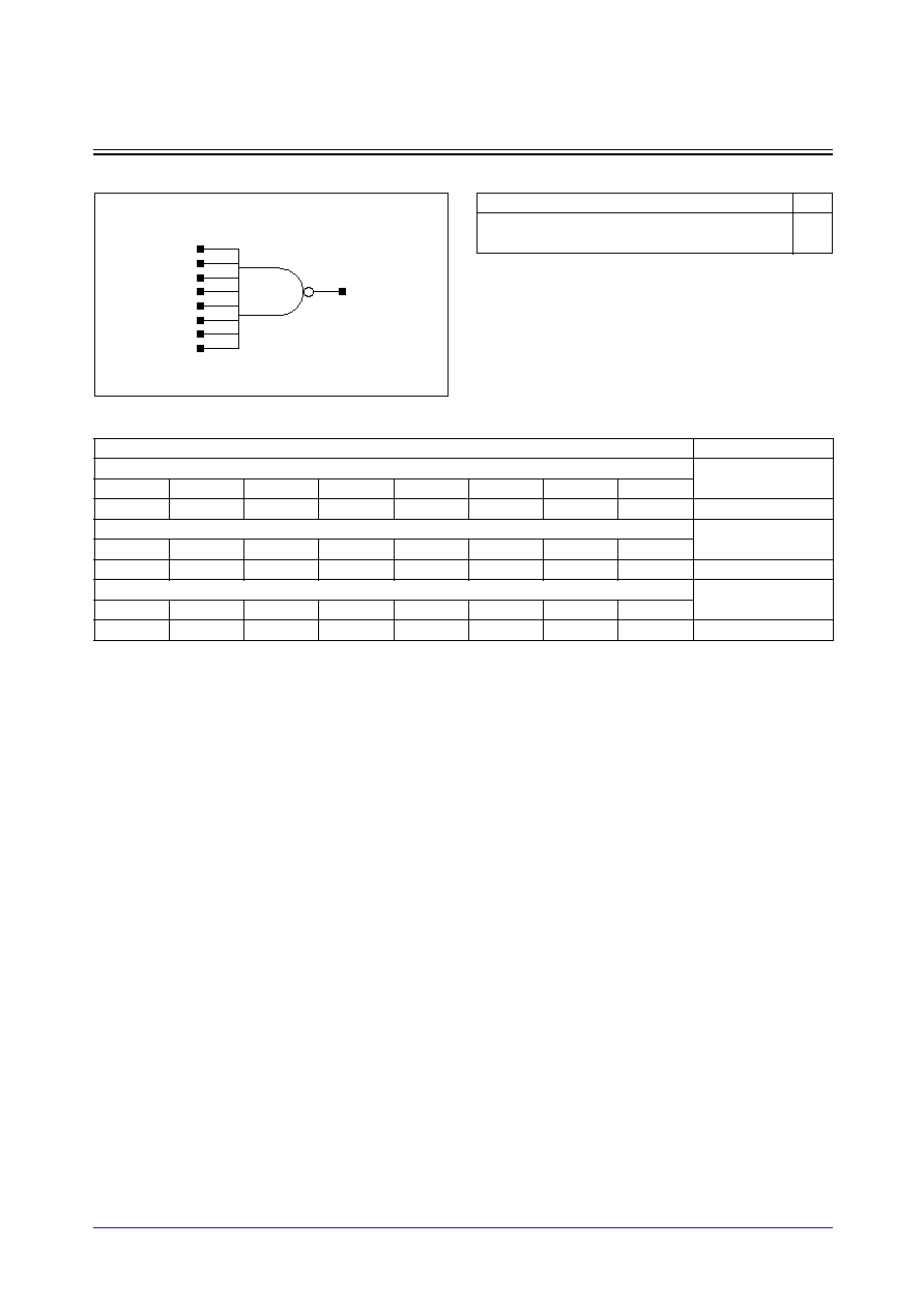
STDL131
3-44
Samsung ASIC
ND8_LP/ND8D2_LP/ND8D4_LP
8-Input NAND with 1X/2X/4X Drive
Logic Symbol
Cell Data
Input Load (SL)
Gate Count
ND8_LP
ND8_LP
A
B
C
D
E
F
G
H
0.7
0.7
0.7
0.7
0.7
0.7
0.7
0.8
4.33
ND8D2_LP
ND8D2_LP
A
B
C
D
E
F
G
H
0.7
0.7
0.7
0.7
0.7
0.7
0.7
0.7
4.67
ND8D4_LP
ND8D4_LP
A
B
C
D
E
F
G
H
0.6
0.6
0.6
0.6
0.6
0.6
0.6
0.6
5.33
C
D
E
Y
F
B
G
A
H
Truth Table
A
B
C
D
E
F
G
H
Y
1
1
1
1
1
1
1
1
0
Other States
1

Samsung ASIC
3-45
STDL131
ND8_LP/ND8D2_LP/ND8D4_LP
8-Input NAND with 1X/2X/4X Drive
Switching Characteristics
(Typical process, 25
∞
C, 1.8V, t
R
/t
F
= 0.19ns, SL: Standard Load)
ND8_LP
Path
Parameter
Delay [ns]
SL = 2
Delay Equations [ns]
Group1*
Group2*
Group3*
A to Y
tR
0.091
0.041 + 0.025*SL
0.037 + 0.026*SL
0.033 + 0.027*SL
tF
0.085
0.049 + 0.018*SL
0.055 + 0.017*SL
0.053 + 0.017*SL
tPLH
0.269
0.243 + 0.013*SL
0.245 + 0.013*SL
0.246 + 0.013*SL
tPHL
0.283
0.255 + 0.014*SL
0.266 + 0.011*SL
0.274 + 0.010*SL
B to Y
tR
0.091
0.040 + 0.026*SL
0.038 + 0.026*SL
0.033 + 0.027*SL
tF
0.086
0.052 + 0.017*SL
0.052 + 0.017*SL
0.052 + 0.017*SL
tPLH
0.290
0.263 + 0.013*SL
0.266 + 0.013*SL
0.266 + 0.013*SL
tPHL
0.292
0.264 + 0.014*SL
0.274 + 0.011*SL
0.283 + 0.010*SL
C to Y
tR
0.092
0.042 + 0.025*SL
0.038 + 0.026*SL
0.032 + 0.027*SL
tF
0.086
0.052 + 0.017*SL
0.053 + 0.017*SL
0.051 + 0.017*SL
tPLH
0.307
0.281 + 0.013*SL
0.283 + 0.013*SL
0.284 + 0.013*SL
tPHL
0.298
0.270 + 0.014*SL
0.280 + 0.011*SL
0.289 + 0.010*SL
D to Y
tR
0.091
0.041 + 0.025*SL
0.036 + 0.026*SL
0.034 + 0.027*SL
tF
0.086
0.052 + 0.017*SL
0.054 + 0.017*SL
0.053 + 0.017*SL
tPLH
0.324
0.297 + 0.013*SL
0.299 + 0.013*SL
0.301 + 0.013*SL
tPHL
0.301
0.274 + 0.014*SL
0.284 + 0.011*SL
0.292 + 0.010*SL
E to Y
tR
0.092
0.041 + 0.026*SL
0.039 + 0.026*SL
0.033 + 0.027*SL
tF
0.086
0.052 + 0.017*SL
0.052 + 0.017*SL
0.052 + 0.017*SL
tPLH
0.281
0.254 + 0.013*SL
0.256 + 0.013*SL
0.257 + 0.013*SL
tPHL
0.304
0.276 + 0.014*SL
0.286 + 0.011*SL
0.295 + 0.010*SL
F to Y
tR
0.091
0.041 + 0.025*SL
0.036 + 0.027*SL
0.035 + 0.027*SL
tF
0.085
0.051 + 0.017*SL
0.052 + 0.017*SL
0.052 + 0.017*SL
tPLH
0.302
0.275 + 0.013*SL
0.277 + 0.013*SL
0.278 + 0.013*SL
tPHL
0.315
0.287 + 0.014*SL
0.297 + 0.011*SL
0.306 + 0.010*SL
G to Y
tR
0.092
0.041 + 0.026*SL
0.038 + 0.026*SL
0.035 + 0.027*SL
tF
0.085
0.048 + 0.018*SL
0.054 + 0.017*SL
0.053 + 0.017*SL
tPLH
0.320
0.294 + 0.013*SL
0.296 + 0.013*SL
0.297 + 0.013*SL
tPHL
0.321
0.293 + 0.014*SL
0.304 + 0.011*SL
0.312 + 0.010*SL
H to Y
tR
0.093
0.043 + 0.025*SL
0.039 + 0.026*SL
0.033 + 0.027*SL
tF
0.085
0.049 + 0.018*SL
0.054 + 0.017*SL
0.053 + 0.017*SL
tPLH
0.335
0.309 + 0.013*SL
0.311 + 0.013*SL
0.312 + 0.013*SL
tPHL
0.323
0.296 + 0.014*SL
0.306 + 0.011*SL
0.314 + 0.010*SL
*Group1 : SL < 4, *Group2 : 4 SL
<
<
=
= 8, *Group3 : 8 < SL

STDL131
3-46
Samsung ASIC
ND8_LP/ND8D2_LP/ND8D4_LP
8-Input NAND with 1X/2X/4X Drive
Switching Characteristics
(Typical process, 25
∞
C, 1.8V, t
R
/t
F
= 0.19ns, SL: Standard Load)
ND8D2_LP
Path
Parameter
Delay [ns]
SL = 2
Delay Equations [ns]
Group1*
Group2*
Group3*
A to Y
tR
0.064
0.039 + 0.012*SL
0.037 + 0.013*SL
0.031 + 0.013*SL
tF
0.074
0.053 + 0.010*SL
0.060 + 0.009*SL
0.063 + 0.008*SL
tPLH
0.278
0.263 + 0.008*SL
0.267 + 0.006*SL
0.270 + 0.006*SL
tPHL
0.296
0.278 + 0.009*SL
0.288 + 0.007*SL
0.304 + 0.005*SL
B to Y
tR
0.064
0.041 + 0.012*SL
0.037 + 0.013*SL
0.031 + 0.013*SL
tF
0.073
0.052 + 0.011*SL
0.060 + 0.009*SL
0.062 + 0.008*SL
tPLH
0.301
0.286 + 0.008*SL
0.291 + 0.006*SL
0.293 + 0.006*SL
tPHL
0.305
0.287 + 0.009*SL
0.297 + 0.007*SL
0.312 + 0.005*SL
C to Y
tR
0.064
0.040 + 0.012*SL
0.038 + 0.013*SL
0.031 + 0.013*SL
tF
0.074
0.053 + 0.010*SL
0.060 + 0.008*SL
0.062 + 0.008*SL
tPLH
0.321
0.306 + 0.008*SL
0.311 + 0.006*SL
0.313 + 0.006*SL
tPHL
0.311
0.293 + 0.009*SL
0.303 + 0.007*SL
0.318 + 0.005*SL
D to Y
tR
0.066
0.043 + 0.012*SL
0.039 + 0.013*SL
0.032 + 0.013*SL
tF
0.074
0.054 + 0.010*SL
0.060 + 0.008*SL
0.062 + 0.008*SL
tPLH
0.341
0.326 + 0.008*SL
0.330 + 0.007*SL
0.333 + 0.006*SL
tPHL
0.315
0.296 + 0.009*SL
0.306 + 0.007*SL
0.322 + 0.005*SL
E to Y
tR
0.066
0.043 + 0.012*SL
0.038 + 0.013*SL
0.032 + 0.013*SL
tF
0.073
0.052 + 0.010*SL
0.059 + 0.009*SL
0.063 + 0.008*SL
tPLH
0.290
0.275 + 0.008*SL
0.279 + 0.007*SL
0.282 + 0.006*SL
tPHL
0.319
0.301 + 0.009*SL
0.311 + 0.007*SL
0.327 + 0.005*SL
F to Y
tR
0.066
0.044 + 0.011*SL
0.039 + 0.013*SL
0.032 + 0.013*SL
tF
0.073
0.053 + 0.010*SL
0.059 + 0.009*SL
0.063 + 0.008*SL
tPLH
0.314
0.298 + 0.008*SL
0.303 + 0.007*SL
0.305 + 0.006*SL
tPHL
0.330
0.312 + 0.009*SL
0.322 + 0.007*SL
0.338 + 0.005*SL
G to Y
tR
0.067
0.044 + 0.011*SL
0.039 + 0.013*SL
0.032 + 0.013*SL
tF
0.074
0.053 + 0.010*SL
0.060 + 0.009*SL
0.063 + 0.008*SL
tPLH
0.335
0.320 + 0.008*SL
0.324 + 0.007*SL
0.327 + 0.006*SL
tPHL
0.337
0.318 + 0.009*SL
0.329 + 0.007*SL
0.344 + 0.005*SL
H to Y
tR
0.066
0.041 + 0.012*SL
0.040 + 0.013*SL
0.033 + 0.013*SL
tF
0.074
0.053 + 0.010*SL
0.060 + 0.009*SL
0.063 + 0.008*SL
tPLH
0.352
0.337 + 0.008*SL
0.341 + 0.007*SL
0.344 + 0.006*SL
tPHL
0.339
0.320 + 0.009*SL
0.331 + 0.007*SL
0.347 + 0.005*SL
*Group1 : SL < 4, *Group2 : 4 SL
<
<
=
= 12, *Group3 : 12 < SL

Samsung ASIC
3-47
STDL131
ND8_LP/ND8D2_LP/ND8D4_LP
8-Input NAND with 1X/2X/4X Drive
Switching Characteristics
(Typical process, 25
∞
C, 1.8V, t
R
/t
F
= 0.19ns, SL: Standard Load)
ND8D4_LP
Path
Parameter
Delay [ns]
SL = 2
Delay Equations [ns]
Group1*
Group2*
Group3*
A to Y
tR
0.065
0.052 + 0.006*SL
0.054 + 0.006*SL
0.045 + 0.006*SL
tF
0.086
0.074 + 0.006*SL
0.080 + 0.005*SL
0.092 + 0.004*SL
tPLH
0.340
0.330 + 0.005*SL
0.336 + 0.004*SL
0.345 + 0.003*SL
tPHL
0.347
0.334 + 0.007*SL
0.344 + 0.004*SL
0.369 + 0.003*SL
B to Y
tR
0.066
0.055 + 0.006*SL
0.054 + 0.006*SL
0.043 + 0.006*SL
tF
0.086
0.073 + 0.006*SL
0.080 + 0.005*SL
0.091 + 0.004*SL
tPLH
0.373
0.363 + 0.005*SL
0.369 + 0.004*SL
0.377 + 0.003*SL
tPHL
0.357
0.344 + 0.006*SL
0.353 + 0.004*SL
0.378 + 0.003*SL
C to Y
tR
0.066
0.054 + 0.006*SL
0.054 + 0.006*SL
0.045 + 0.006*SL
tF
0.087
0.073 + 0.007*SL
0.082 + 0.005*SL
0.090 + 0.004*SL
tPLH
0.402
0.392 + 0.005*SL
0.397 + 0.004*SL
0.406 + 0.003*SL
tPHL
0.363
0.350 + 0.006*SL
0.359 + 0.004*SL
0.384 + 0.003*SL
D to Y
tR
0.068
0.055 + 0.006*SL
0.056 + 0.006*SL
0.046 + 0.006*SL
tF
0.086
0.074 + 0.006*SL
0.080 + 0.005*SL
0.092 + 0.004*SL
tPLH
0.431
0.421 + 0.005*SL
0.426 + 0.004*SL
0.436 + 0.003*SL
tPHL
0.366
0.354 + 0.006*SL
0.362 + 0.004*SL
0.388 + 0.003*SL
E to Y
tR
0.066
0.053 + 0.006*SL
0.054 + 0.006*SL
0.044 + 0.006*SL
tF
0.086
0.073 + 0.006*SL
0.079 + 0.005*SL
0.092 + 0.004*SL
tPLH
0.349
0.339 + 0.005*SL
0.345 + 0.004*SL
0.353 + 0.003*SL
tPHL
0.372
0.359 + 0.006*SL
0.368 + 0.004*SL
0.394 + 0.003*SL
F to Y
tR
0.066
0.054 + 0.006*SL
0.054 + 0.006*SL
0.045 + 0.006*SL
tF
0.086
0.073 + 0.006*SL
0.080 + 0.005*SL
0.093 + 0.004*SL
tPLH
0.383
0.373 + 0.005*SL
0.378 + 0.004*SL
0.387 + 0.003*SL
tPHL
0.380
0.367 + 0.006*SL
0.375 + 0.004*SL
0.401 + 0.003*SL
G to Y
tR
0.067
0.055 + 0.006*SL
0.055 + 0.006*SL
0.043 + 0.006*SL
tF
0.086
0.073 + 0.006*SL
0.079 + 0.005*SL
0.092 + 0.004*SL
tPLH
0.414
0.404 + 0.005*SL
0.409 + 0.004*SL
0.418 + 0.003*SL
tPHL
0.388
0.375 + 0.006*SL
0.383 + 0.004*SL
0.409 + 0.003*SL
H to Y
tR
0.066
0.055 + 0.005*SL
0.053 + 0.006*SL
0.044 + 0.006*SL
tF
0.086
0.073 + 0.007*SL
0.080 + 0.005*SL
0.091 + 0.004*SL
tPLH
0.439
0.429 + 0.005*SL
0.434 + 0.004*SL
0.443 + 0.003*SL
tPHL
0.390
0.377 + 0.006*SL
0.386 + 0.004*SL
0.412 + 0.003*SL
*Group1 : SL < 4, *Group2 : 4 SL
<
<
=
= 20, *Group3 : 20 < SL
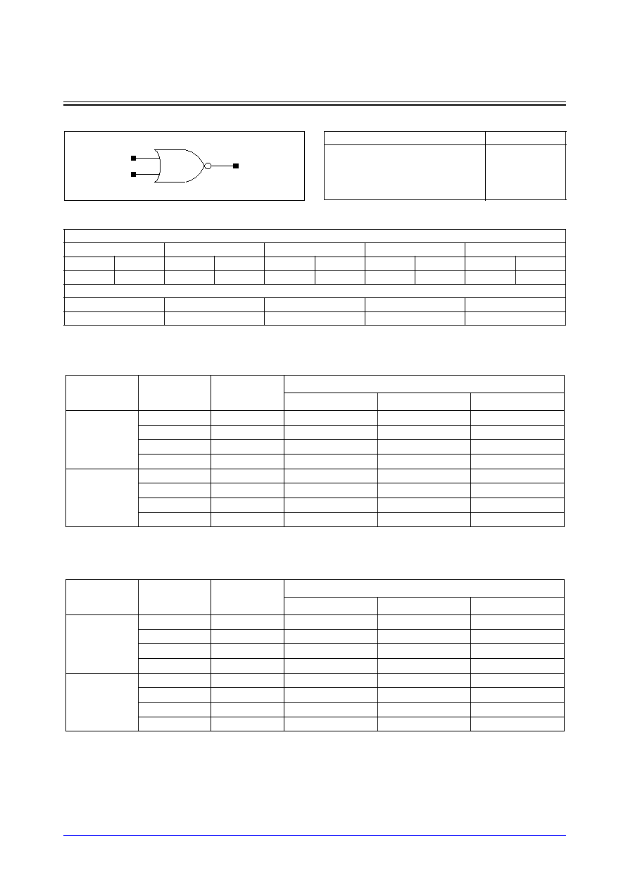
STDL131
3-48
Samsung ASIC
NR2_LP/NR2A_LP/NR2D2_LP/NR2D4_LP/NR2D8_LP
2-Input NOR with 1X/2X P-Tr, 1X N-Tr/2X/4X/8X Drive
Logic Symbol
Cell Data
Switching Characteristics
(Typical process, 25
∞
C, 1.8V, t
R
/t
F
= 0.19ns, SL: Standard Load)
NR2_LP
NR2A_LP
Input Load (SL)
NR2_LP
NR2A_LP
NR2D2_LP
NR2D4_LP
NR2D8_LP
A
B
A
B
A
B
A
B
A
B
1.1
1.1
1.8
1.9
2.2
2.3
0.8
0.8
1.1
1.1
Gate Count
NR2_LP
NR2A_LP
NR2D2_LP
NR2D4_LP
NR2D8_LP
1.00
1.67
1.67
2.67
4.33
Y
A
B
Path
Parameter
Delay [ns]
SL = 2
Delay Equations [ns]
Group1*
Group2*
Group3*
A to Y
tR
0.203
0.104 + 0.049*SL
0.094 + 0.052*SL
0.083 + 0.053*SL
tF
0.085
0.058 + 0.013*SL
0.057 + 0.014*SL
0.046 + 0.015*SL
tPLH
0.141
0.089 + 0.026*SL
0.089 + 0.026*SL
0.089 + 0.026*SL
tPHL
0.073
0.047 + 0.013*SL
0.061 + 0.009*SL
0.065 + 0.009*SL
B to Y
tR
0.194
0.090 + 0.052*SL
0.086 + 0.053*SL
0.081 + 0.053*SL
tF
0.095
0.068 + 0.014*SL
0.068 + 0.014*SL
0.058 + 0.015*SL
tPLH
0.159
0.107 + 0.026*SL
0.108 + 0.026*SL
0.108 + 0.026*SL
tPHL
0.085
0.062 + 0.012*SL
0.072 + 0.009*SL
0.073 + 0.009*SL
*Group1 : SL < 4, *Group2 : 4 SL
<
<
=
= 8, *Group3 : 8 < SL
Path
Parameter
Delay [ns]
SL = 2
Delay Equations [ns]
Group1*
Group2*
Group3*
A to Y
tR
0.137
0.092 + 0.023*SL
0.083 + 0.025*SL
0.075 + 0.026*SL
tF
0.095
0.063 + 0.016*SL
0.056 + 0.018*SL
0.050 + 0.019*SL
tPLH
0.100
0.070 + 0.015*SL
0.077 + 0.013*SL
0.077 + 0.013*SL
tPHL
0.092
0.066 + 0.013*SL
0.075 + 0.011*SL
0.077 + 0.011*SL
B to Y
tR
0.122
0.072 + 0.025*SL
0.069 + 0.026*SL
0.065 + 0.026*SL
tF
0.120
0.085 + 0.017*SL
0.083 + 0.018*SL
0.074 + 0.019*SL
tPLH
0.120
0.093 + 0.014*SL
0.096 + 0.013*SL
0.096 + 0.013*SL
tPHL
0.119
0.096 + 0.012*SL
0.098 + 0.011*SL
0.100 + 0.011*SL
*Group1 : SL < 4, *Group2 : 4 SL
<
<
=
= 8, *Group3 : 8 < SL
Truth Table
A
B
Y
0
0
1
0
1
0
1
0
0
1
1
0
Samsung ASIC
3-49
STDL131
NR2_LP/NR2A_LP/NR2D2_LP/NR2D4_LP/NR2D8_LP
2-Input NOR with 1X/2X P-Tr, 1X N-Tr/2X/4X/8X Drive
Switching Characteristics
(Typical process, 25
∞
C, 1.8V, t
R
/t
F
= 0.19ns, SL: Standard Load)
NR2D2_LP
NR2D4_LP
NR2D8_LP
Path
Parameter
Delay [ns]
SL = 2
Delay Equations [ns]
Group1*
Group2*
Group3*
A to Y
tR
0.147
0.101 + 0.023*SL
0.092 + 0.025*SL
0.078 + 0.026*SL
tF
0.067
0.050 + 0.008*SL
0.057 + 0.007*SL
0.047 + 0.007*SL
tPLH
0.110
0.083 + 0.014*SL
0.085 + 0.013*SL
0.085 + 0.013*SL
tPHL
0.056
0.039 + 0.008*SL
0.050 + 0.006*SL
0.063 + 0.004*SL
B to Y
tR
0.134
0.084 + 0.025*SL
0.079 + 0.026*SL
0.073 + 0.027*SL
tF
0.079
0.065 + 0.007*SL
0.065 + 0.007*SL
0.060 + 0.007*SL
tPLH
0.129
0.102 + 0.014*SL
0.104 + 0.013*SL
0.104 + 0.013*SL
tPHL
0.070
0.056 + 0.007*SL
0.064 + 0.005*SL
0.071 + 0.004*SL
*Group1 : SL < 4, *Group2 : 4 SL
<
<
=
= 12, *Group3 : 12 < SL
Path
Parameter
Delay [ns]
SL = 2
Delay Equations [ns]
Group1*
Group2*
Group3*
A to Y
tR
0.061
0.047 + 0.007*SL
0.050 + 0.006*SL
0.041 + 0.006*SL
tF
0.055
0.046 + 0.004*SL
0.047 + 0.004*SL
0.048 + 0.004*SL
tPLH
0.276
0.266 + 0.005*SL
0.271 + 0.004*SL
0.279 + 0.003*SL
tPHL
0.217
0.207 + 0.005*SL
0.214 + 0.003*SL
0.228 + 0.003*SL
B to Y
tR
0.062
0.051 + 0.005*SL
0.048 + 0.006*SL
0.040 + 0.007*SL
tF
0.055
0.047 + 0.004*SL
0.046 + 0.004*SL
0.049 + 0.004*SL
tPLH
0.295
0.286 + 0.005*SL
0.291 + 0.004*SL
0.298 + 0.003*SL
tPHL
0.232
0.223 + 0.005*SL
0.229 + 0.003*SL
0.243 + 0.003*SL
*Group1 : SL < 4, *Group2 : 4 SL
<
<
=
= 20, *Group3 : 20 < SL
Path
Parameter
Delay [ns]
SL = 2
Delay Equations [ns]
Group1*
Group2*
Group3*
A to Y
tR
0.057
0.050 + 0.004*SL
0.053 + 0.003*SL
0.044 + 0.003*SL
tF
0.049
0.043 + 0.003*SL
0.046 + 0.002*SL
0.045 + 0.002*SL
tPLH
0.298
0.292 + 0.003*SL
0.296 + 0.002*SL
0.307 + 0.002*SL
tPHL
0.209
0.204 + 0.003*SL
0.207 + 0.002*SL
0.223 + 0.001*SL
B to Y
tR
0.058
0.051 + 0.003*SL
0.052 + 0.003*SL
0.044 + 0.003*SL
tF
0.050
0.045 + 0.002*SL
0.046 + 0.002*SL
0.048 + 0.002*SL
tPLH
0.318
0.312 + 0.003*SL
0.316 + 0.002*SL
0.326 + 0.002*SL
tPHL
0.222
0.217 + 0.003*SL
0.220 + 0.002*SL
0.236 + 0.001*SL
*Group1 : SL < 4, *Group2 : 4 SL
<
<
=
= 37, *Group3 : 37 < SL
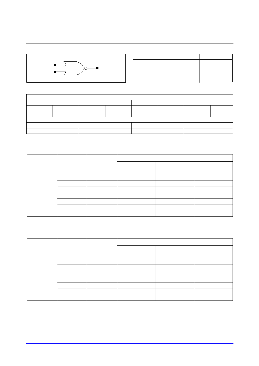
STDL131
3-50
Samsung ASIC
NR2B_LP/NR2BD2_LP/NR2BD4_LP/NR2BD8_LP
2-Input NOR with one Inverted Input, 1X/2X/4X/8X Drive
Logic Symbol
Cell Data
Switching Characteristics
(Typical process, 25
∞
C, 1.8V, t
R
/t
F
= 0.19ns, SL: Standard Load)
NR2B_LP
NR2BD2_LP
Input Load (SL)
NR2B_LP
NR2BD2_LP
NR2BD4_LP
NR2BD8_LP
AN
B
AN
B
AN
B
AN
B
0.6
1.2
0.8
2.3
0.5
0.8
0.6
1.1
Gate Count
NR2B_LP
NR2BD2_LP
NR2BD4_LP
NR2BD8_LP
1.33
2.00
3.33
5.00
Truth Table
AN
B
Y
0
0
0
0
1
0
1
0
1
1
1
0
Y
AN
B
Path
Parameter
Delay [ns]
SL = 2
Delay Equations [ns]
Group1*
Group2*
Group3*
AN to Y
tR
0.193
0.086 + 0.053*SL
0.083 + 0.054*SL
0.082 + 0.054*SL
tF
0.074
0.044 + 0.015*SL
0.044 + 0.015*SL
0.041 + 0.016*SL
tPLH
0.182
0.128 + 0.027*SL
0.129 + 0.026*SL
0.131 + 0.026*SL
tPHL
0.172
0.149 + 0.011*SL
0.156 + 0.009*SL
0.160 + 0.009*SL
B to Y
tR
0.197
0.093 + 0.052*SL
0.088 + 0.053*SL
0.083 + 0.054*SL
tF
0.096
0.069 + 0.014*SL
0.069 + 0.014*SL
0.058 + 0.015*SL
tPLH
0.163
0.110 + 0.027*SL
0.111 + 0.026*SL
0.111 + 0.026*SL
tPHL
0.085
0.062 + 0.012*SL
0.072 + 0.009*SL
0.073 + 0.009*SL
*Group1 : SL < 4, *Group2 : 4 SL
<
<
=
= 8, *Group3 : 8 < SL
Path
Parameter
Delay [ns]
SL = 2
Delay Equations [ns]
Group1*
Group2*
Group3*
AN to Y
tR
0.133
0.081 + 0.026*SL
0.078 + 0.027*SL
0.075 + 0.027*SL
tF
0.062
0.046 + 0.008*SL
0.048 + 0.007*SL
0.045 + 0.008*SL
tPLH
0.171
0.144 + 0.013*SL
0.145 + 0.013*SL
0.147 + 0.013*SL
tPHL
0.171
0.158 + 0.007*SL
0.164 + 0.005*SL
0.172 + 0.005*SL
B to Y
tR
0.137
0.087 + 0.025*SL
0.083 + 0.026*SL
0.076 + 0.027*SL
tF
0.081
0.067 + 0.007*SL
0.067 + 0.007*SL
0.061 + 0.007*SL
tPLH
0.133
0.105 + 0.014*SL
0.107 + 0.013*SL
0.108 + 0.013*SL
tPHL
0.069
0.055 + 0.007*SL
0.063 + 0.005*SL
0.071 + 0.004*SL
*Group1 : SL < 4, *Group2 : 4 SL
<
<
=
= 12, *Group3 : 12 < SL

Samsung ASIC
3-51
STDL131
NR2B_LP/NR2BD2_LP/NR2BD4_LP/NR2BD8_LP
2-Input NOR with one Inverted Input, 1X/2X/4X/8X Drive
Switching Characteristics
(Typical process, 25
∞
C, 1.8V, t
R
/t
F
= 0.19ns, SL: Standard Load)
NR2BD4_LP
NR2BD8_LP
Path
Parameter
Delay [ns]
SL = 2
Delay Equations [ns]
Group1*
Group2*
Group3*
AN to Y
tR
0.061
0.051 + 0.005*SL
0.047 + 0.006*SL
0.039 + 0.007*SL
tF
0.054
0.045 + 0.005*SL
0.047 + 0.004*SL
0.047 + 0.004*SL
tPLH
0.314
0.305 + 0.005*SL
0.310 + 0.004*SL
0.317 + 0.003*SL
tPHL
0.308
0.299 + 0.005*SL
0.305 + 0.003*SL
0.319 + 0.003*SL
B to Y
tR
0.060
0.046 + 0.007*SL
0.050 + 0.006*SL
0.041 + 0.006*SL
tF
0.055
0.047 + 0.004*SL
0.046 + 0.004*SL
0.049 + 0.004*SL
tPLH
0.295
0.286 + 0.005*SL
0.291 + 0.004*SL
0.298 + 0.003*SL
tPHL
0.231
0.221 + 0.005*SL
0.227 + 0.003*SL
0.241 + 0.003*SL
*Group1 : SL < 4, *Group2 : 4 SL
<
<
=
= 20, *Group3 : 20 < SL
Path
Parameter
Delay [ns]
SL = 2
Delay Equations [ns]
Group1*
Group2*
Group3*
AN to Y
tR
0.059
0.053 + 0.003*SL
0.053 + 0.003*SL
0.044 + 0.003*SL
tF
0.048
0.044 + 0.002*SL
0.044 + 0.002*SL
0.045 + 0.002*SL
tPLH
0.339
0.334 + 0.003*SL
0.337 + 0.002*SL
0.348 + 0.002*SL
tPHL
0.308
0.303 + 0.003*SL
0.306 + 0.002*SL
0.322 + 0.001*SL
B to Y
tR
0.059
0.053 + 0.003*SL
0.053 + 0.003*SL
0.043 + 0.003*SL
tF
0.049
0.044 + 0.003*SL
0.046 + 0.002*SL
0.047 + 0.002*SL
tPLH
0.319
0.314 + 0.003*SL
0.317 + 0.002*SL
0.327 + 0.002*SL
tPHL
0.220
0.215 + 0.003*SL
0.219 + 0.002*SL
0.234 + 0.001*SL
*Group1 : SL < 4, *Group2 : 4 SL
<
<
=
= 37, *Group3 : 37 < SL
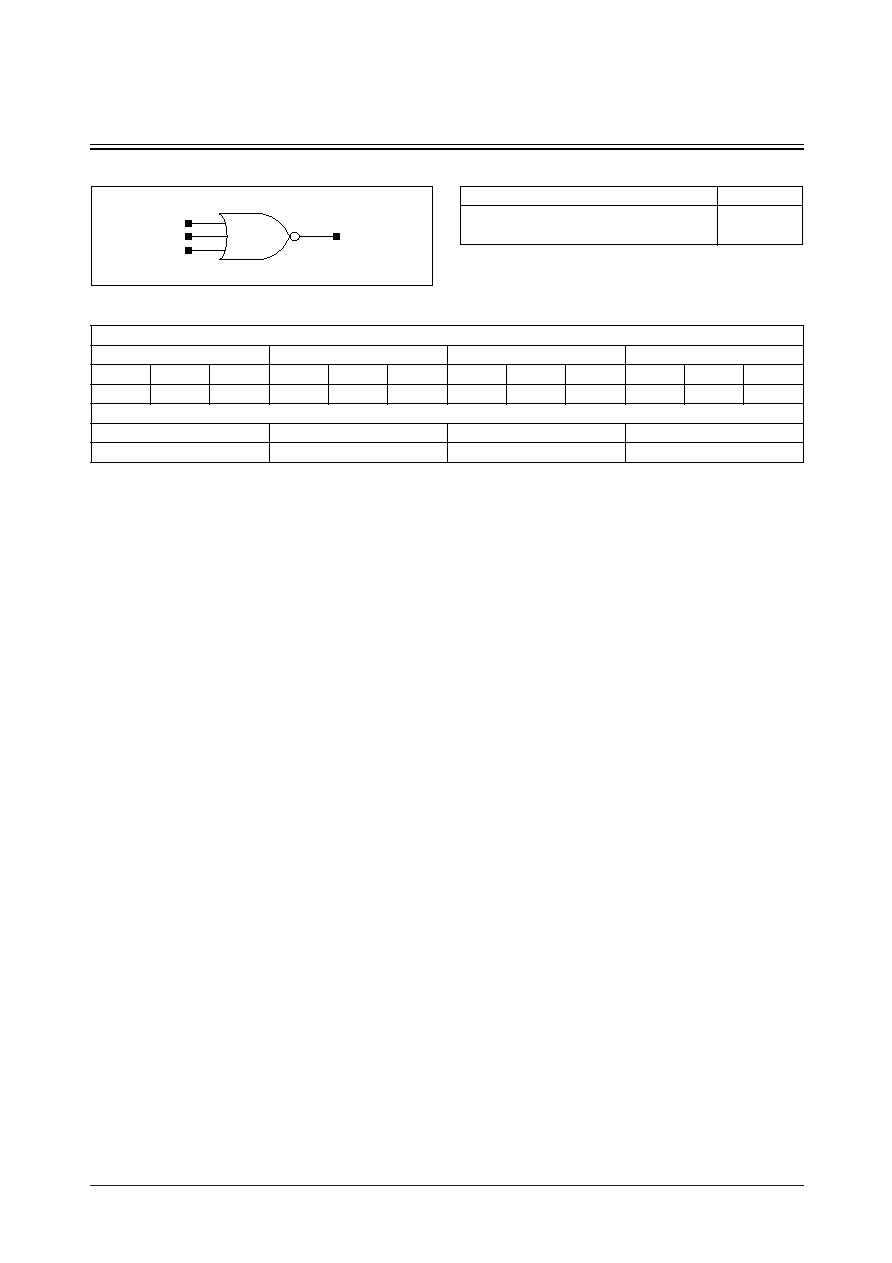
STDL131
3-52
Samsung ASIC
NR3_LP/NR3A_LP/NR3D2_LP/NR3D4_LP
3-Input NOR with 1X/2X P-Tr, 1X N-Tr/2X/4X/8X Drive
Logic Symbol
Cell Data
Input Load (SL)
NR3_LP
NR3A_LP
NR3D2_LP
NR3D4_LP
A
B
C
A
B
C
A
B
C
A
B
C
1.0
1.0
1.0
1.7
1.8
1.8
2.0
2.0
1.9
0.9
0.9
0.9
Gate Count
NR3_LP
NR3A_LP
NR3D2_LP
NR3D4_LP
1.33
2.00
2.33
3.00
Y
A
B
C
Truth Table
A
B
C
Y
0
0
0
1
Other States
0
Samsung ASIC
3-53
STDL131
NR3_LP/NR3A_LP/NR3D2_LP/NR3D4_LP
3-Input NOR with 1X/2X P-Tr, 1X N-Tr/2X/4X/8X Drive
Switching Characteristics
(Typical process, 25
∞
C, 1.8V, t
R
/t
F
= 0.19ns, SL: Standard Load)
NR3_LP
NR3A_LP
Path
Parameter
Delay [ns]
SL = 2
Delay Equations [ns]
Group1*
Group2*
Group3*
A to Y
tR
0.310
0.156 + 0.077*SL
0.145 + 0.080*SL
0.141 + 0.080*SL
tF
0.110
0.064 + 0.023*SL
0.057 + 0.025*SL
0.048 + 0.026*SL
tPLH
0.175
0.097 + 0.039*SL
0.096 + 0.039*SL
0.097 + 0.039*SL
tPHL
0.103
0.071 + 0.016*SL
0.077 + 0.015*SL
0.078 + 0.015*SL
B to Y
tR
0.310
0.153 + 0.079*SL
0.148 + 0.080*SL
0.145 + 0.080*SL
tF
0.128
0.081 + 0.023*SL
0.074 + 0.025*SL
0.066 + 0.026*SL
tPLH
0.221
0.142 + 0.040*SL
0.143 + 0.039*SL
0.143 + 0.039*SL
tPHL
0.121
0.090 + 0.015*SL
0.092 + 0.015*SL
0.094 + 0.015*SL
C to Y
tR
0.308
0.150 + 0.079*SL
0.147 + 0.080*SL
0.145 + 0.080*SL
tF
0.145
0.097 + 0.024*SL
0.091 + 0.026*SL
0.086 + 0.026*SL
tPLH
0.239
0.160 + 0.039*SL
0.161 + 0.039*SL
0.162 + 0.039*SL
tPHL
0.128
0.096 + 0.016*SL
0.098 + 0.015*SL
0.102 + 0.015*SL
*Group1 : SL < 4, *Group2 : 4 SL
<
<
=
= 8, *Group3 : 8 < SL
Path
Parameter
Delay [ns]
SL = 2
Delay Equations [ns]
Group1*
Group2*
Group3*
A to Y
tR
0.205
0.129 + 0.038*SL
0.123 + 0.040*SL
0.114 + 0.041*SL
tF
0.118
0.070 + 0.024*SL
0.062 + 0.026*SL
0.052 + 0.027*SL
tPLH
0.120
0.081 + 0.020*SL
0.079 + 0.020*SL
0.079 + 0.020*SL
tPHL
0.118
0.085 + 0.016*SL
0.088 + 0.015*SL
0.090 + 0.015*SL
B to Y
tR
0.202
0.124 + 0.039*SL
0.119 + 0.040*SL
0.116 + 0.041*SL
tF
0.153
0.100 + 0.026*SL
0.098 + 0.027*SL
0.092 + 0.027*SL
tPLH
0.166
0.125 + 0.020*SL
0.126 + 0.020*SL
0.127 + 0.020*SL
tPHL
0.154
0.121 + 0.016*SL
0.124 + 0.016*SL
0.127 + 0.015*SL
C to Y
tR
0.200
0.120 + 0.040*SL
0.117 + 0.041*SL
0.114 + 0.041*SL
tF
0.189
0.134 + 0.028*SL
0.136 + 0.027*SL
0.133 + 0.028*SL
tPLH
0.184
0.143 + 0.020*SL
0.144 + 0.020*SL
0.145 + 0.020*SL
tPHL
0.174
0.139 + 0.018*SL
0.143 + 0.016*SL
0.149 + 0.016*SL
*Group1 : SL < 4, *Group2 : 4 SL
<
<
=
= 8, *Group3 : 8 < SL

STDL131
3-54
Samsung ASIC
NR3_LP/NR3A_LP/NR3D2_LP/NR3D4_LP
3-Input NOR with 1X/2X P-Tr, 1X N-Tr/2X/4X/8X Drive
Switching Characteristics
(Typical process, 25
∞
C, 1.8V, t
R
/t
F
= 0.19ns, SL: Standard Load)
NR3D2_LP
NR3D4_LP
Path
Parameter
Delay [ns]
SL = 2
Delay Equations [ns]
Group1*
Group2*
Group3*
A to Y
tR
0.238
0.163 + 0.038*SL
0.156 + 0.039*SL
0.145 + 0.040*SL
tF
0.088
0.066 + 0.011*SL
0.062 + 0.012*SL
0.051 + 0.013*SL
tPLH
0.138
0.100 + 0.019*SL
0.098 + 0.020*SL
0.098 + 0.020*SL
tPHL
0.087
0.068 + 0.010*SL
0.076 + 0.007*SL
0.079 + 0.007*SL
B to Y
tR
0.236
0.159 + 0.039*SL
0.154 + 0.040*SL
0.150 + 0.040*SL
tF
0.105
0.082 + 0.011*SL
0.078 + 0.012*SL
0.069 + 0.013*SL
tPLH
0.183
0.144 + 0.020*SL
0.144 + 0.020*SL
0.145 + 0.020*SL
tPHL
0.106
0.089 + 0.008*SL
0.092 + 0.008*SL
0.095 + 0.007*SL
C to Y
tR
0.233
0.155 + 0.039*SL
0.153 + 0.040*SL
0.150 + 0.040*SL
tF
0.121
0.097 + 0.012*SL
0.096 + 0.012*SL
0.089 + 0.013*SL
tPLH
0.202
0.162 + 0.020*SL
0.162 + 0.020*SL
0.163 + 0.020*SL
tPHL
0.113
0.096 + 0.008*SL
0.098 + 0.008*SL
0.102 + 0.008*SL
*Group1 : SL < 4, *Group2 : 4 SL
<
<
=
= 12, *Group3 : 12 < SL
Path
Parameter
Delay [ns]
SL = 2
Delay Equations [ns]
Group1*
Group2*
Group3*
A to Y
tR
0.066
0.054 + 0.006*SL
0.052 + 0.006*SL
0.044 + 0.006*SL
tF
0.055
0.046 + 0.005*SL
0.047 + 0.004*SL
0.050 + 0.004*SL
tPLH
0.318
0.308 + 0.005*SL
0.313 + 0.004*SL
0.322 + 0.003*SL
tPHL
0.236
0.226 + 0.005*SL
0.232 + 0.003*SL
0.246 + 0.003*SL
B to Y
tR
0.067
0.055 + 0.006*SL
0.054 + 0.006*SL
0.042 + 0.007*SL
tF
0.055
0.045 + 0.005*SL
0.047 + 0.004*SL
0.049 + 0.004*SL
tPLH
0.366
0.356 + 0.005*SL
0.362 + 0.004*SL
0.370 + 0.003*SL
tPHL
0.255
0.246 + 0.005*SL
0.251 + 0.003*SL
0.266 + 0.003*SL
C to Y
tR
0.067
0.055 + 0.006*SL
0.055 + 0.006*SL
0.042 + 0.007*SL
tF
0.055
0.045 + 0.005*SL
0.049 + 0.004*SL
0.049 + 0.004*SL
tPLH
0.384
0.374 + 0.005*SL
0.380 + 0.004*SL
0.388 + 0.003*SL
tPHL
0.266
0.256 + 0.005*SL
0.262 + 0.003*SL
0.277 + 0.003*SL
*Group1 : SL < 4, *Group2 : 4 SL
<
<
=
= 20, *Group3 : 20 < SL
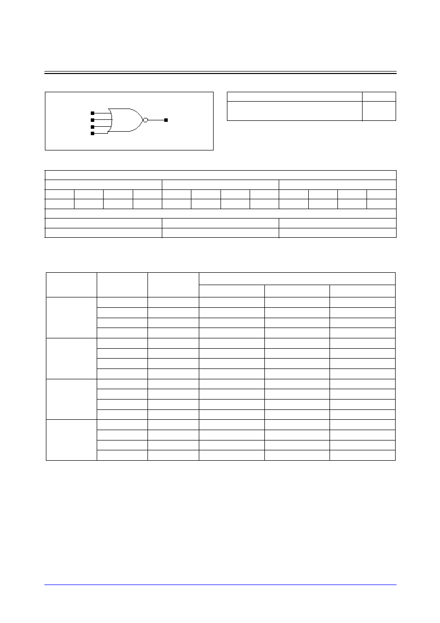
Samsung ASIC
3-55
STDL131
NR4_LP/NR4D2_LP/NR4D4_LP
4-Input NOR with 1X/2X/4X Drive
Logic Symbol
Cell Data
Switching Characteristics
(Typical process, 25
∞
C, 1.8V, t
R
/t
F
= 0.19ns, SL: Standard Load)
NR4_LP
Input Load (SL)
NR4_LP
NR4D2_LP
NR4D4_LP
A
B
C
D
A
B
C
D
A
B
C
D
0.8
0.8
0.8
0.8
0.8
0.8
0.8
0.8
0.8
0.8
0.8
0.8
Gate Count
NR4_LP
NR4D2_LP
NR4D4_LP
3.00
3.33
4.00
Y
A
B
C
D
Path
Parameter
Delay [ns]
SL = 2
Delay Equations [ns]
Group1*
Group2*
Group3*
A to Y
tR
0.104
0.055 + 0.024*SL
0.049 + 0.026*SL
0.045 + 0.026*SL
tF
0.073
0.040 + 0.016*SL
0.039 + 0.017*SL
0.034 + 0.017*SL
tPLH
0.291
0.262 + 0.015*SL
0.268 + 0.013*SL
0.271 + 0.013*SL
tPHL
0.195
0.171 + 0.012*SL
0.178 + 0.010*SL
0.182 + 0.010*SL
B to Y
tR
0.104
0.055 + 0.025*SL
0.052 + 0.025*SL
0.045 + 0.026*SL
tF
0.071
0.037 + 0.017*SL
0.038 + 0.017*SL
0.036 + 0.017*SL
tPLH
0.310
0.281 + 0.015*SL
0.287 + 0.013*SL
0.290 + 0.013*SL
tPHL
0.209
0.185 + 0.012*SL
0.192 + 0.010*SL
0.195 + 0.010*SL
C to Y
tR
0.104
0.054 + 0.025*SL
0.052 + 0.025*SL
0.045 + 0.026*SL
tF
0.073
0.039 + 0.017*SL
0.041 + 0.017*SL
0.036 + 0.017*SL
tPLH
0.285
0.256 + 0.015*SL
0.262 + 0.013*SL
0.265 + 0.013*SL
tPHL
0.201
0.177 + 0.012*SL
0.184 + 0.010*SL
0.188 + 0.010*SL
D to Y
tR
0.103
0.053 + 0.025*SL
0.050 + 0.026*SL
0.044 + 0.026*SL
tF
0.074
0.042 + 0.016*SL
0.041 + 0.017*SL
0.036 + 0.017*SL
tPLH
0.304
0.275 + 0.015*SL
0.281 + 0.013*SL
0.284 + 0.013*SL
tPHL
0.215
0.191 + 0.012*SL
0.198 + 0.010*SL
0.202 + 0.010*SL
*Group1 : SL < 4, *Group2 : 4 SL
<
<
=
= 8, *Group3 : 8 < SL
Truth Table
A
B
C
D
Y
0
0
0
0
1
Other States
0

STDL131
3-56
Samsung ASIC
NR4_LP/NR4D2_LP/NR4D4_LP
4-Input NOR with 1X/2X/4X Drive
Switching Characteristics
(Typical process, 25
∞
C, 1.8V, t
R
/t
F
= 0.19ns, SL: Standard Load)
NR4D2_LP
NR4D4_LP
Path
Parameter
Delay [ns]
SL = 2
Delay Equations [ns]
Group1*
Group2*
Group3*
A to Y
tR
0.073
0.048 + 0.012*SL
0.047 + 0.013*SL
0.041 + 0.013*SL
tF
0.060
0.041 + 0.009*SL
0.046 + 0.008*SL
0.043 + 0.008*SL
tPLH
0.269
0.252 + 0.008*SL
0.258 + 0.007*SL
0.264 + 0.006*SL
tPHL
0.213
0.197 + 0.008*SL
0.205 + 0.006*SL
0.215 + 0.005*SL
B to Y
tR
0.074
0.049 + 0.012*SL
0.048 + 0.012*SL
0.042 + 0.013*SL
tF
0.060
0.042 + 0.009*SL
0.046 + 0.008*SL
0.044 + 0.008*SL
tPLH
0.288
0.271 + 0.008*SL
0.277 + 0.007*SL
0.283 + 0.006*SL
tPHL
0.228
0.212 + 0.008*SL
0.220 + 0.006*SL
0.230 + 0.005*SL
C to Y
tR
0.072
0.046 + 0.013*SL
0.047 + 0.013*SL
0.042 + 0.013*SL
tF
0.062
0.043 + 0.009*SL
0.048 + 0.008*SL
0.046 + 0.008*SL
tPLH
0.263
0.246 + 0.009*SL
0.253 + 0.007*SL
0.259 + 0.006*SL
tPHL
0.222
0.206 + 0.008*SL
0.214 + 0.006*SL
0.225 + 0.005*SL
D to Y
tR
0.073
0.049 + 0.012*SL
0.047 + 0.012*SL
0.040 + 0.013*SL
tF
0.061
0.044 + 0.009*SL
0.045 + 0.008*SL
0.045 + 0.008*SL
tPLH
0.282
0.265 + 0.009*SL
0.272 + 0.007*SL
0.278 + 0.006*SL
tPHL
0.237
0.222 + 0.008*SL
0.230 + 0.006*SL
0.240 + 0.005*SL
*Group1 : SL < 4, *Group2 : 4 SL
<
<
=
= 12, *Group3 : 12 < SL
Path
Parameter
Delay [ns]
SL = 2
Delay Equations [ns]
Group1*
Group2*
Group3*
A to Y
tR
0.075
0.060 + 0.007*SL
0.065 + 0.006*SL
0.060 + 0.006*SL
tF
0.068
0.056 + 0.006*SL
0.063 + 0.004*SL
0.067 + 0.004*SL
tPLH
0.304
0.293 + 0.006*SL
0.300 + 0.004*SL
0.315 + 0.003*SL
tPHL
0.255
0.244 + 0.006*SL
0.252 + 0.004*SL
0.271 + 0.003*SL
B to Y
tR
0.075
0.060 + 0.007*SL
0.065 + 0.006*SL
0.060 + 0.006*SL
tF
0.069
0.058 + 0.005*SL
0.062 + 0.004*SL
0.066 + 0.004*SL
tPLH
0.324
0.312 + 0.006*SL
0.319 + 0.004*SL
0.334 + 0.003*SL
tPHL
0.270
0.259 + 0.006*SL
0.267 + 0.004*SL
0.286 + 0.003*SL
C to Y
tR
0.075
0.061 + 0.007*SL
0.064 + 0.006*SL
0.060 + 0.006*SL
tF
0.070
0.058 + 0.006*SL
0.065 + 0.004*SL
0.070 + 0.004*SL
tPLH
0.296
0.284 + 0.006*SL
0.291 + 0.004*SL
0.306 + 0.003*SL
tPHL
0.263
0.251 + 0.006*SL
0.259 + 0.004*SL
0.279 + 0.003*SL
D to Y
tR
0.075
0.061 + 0.007*SL
0.064 + 0.006*SL
0.059 + 0.006*SL
tF
0.071
0.059 + 0.006*SL
0.065 + 0.004*SL
0.069 + 0.004*SL
tPLH
0.315
0.304 + 0.006*SL
0.310 + 0.004*SL
0.325 + 0.003*SL
tPHL
0.278
0.267 + 0.006*SL
0.275 + 0.004*SL
0.295 + 0.003*SL
*Group1 : SL < 4, *Group2 : 4 SL
<
<
=
= 20, *Group3 : 20 < SL

Samsung ASIC
3-57
STDL131
NR5_LP/NR5D2_LP/NR5D4_LP
5-Input NOR with 1X/2X/4X Drive
Logic Symbol
Cell Data
Input Load (SL)
NR5_LP
NR5D2_LP
NR5D4_LP
A
B
C
D
E
A
B
C
D
E
A
B
C
D
E
0.9
0.9
0.9
0.8
0.8
1.0
1.0
1.0
0.8
0.8
1.0
1.0
1.0
0.8
0.8
Gate Count
NR5_LP
NR5D2_LP
NR5D4_LP
3.33
3.67
4.33
Y
B
C
D
E
A
Truth Table
A
B
C
D
E
Y
0
0
0
0
0
1
Other States
0
STDL131
3-58
Samsung ASIC
NR5_LP/NR5D2_LP/NR5D4_LP
5-Input NOR with 1X/2X/4X Drive
Switching Characteristics
(Typical process, 25
∞
C, 1.8V, t
R
/t
F
= 0.19ns, SL: Standard Load)
NR5_LP
Path
Parameter
Delay [ns]
SL = 2
Delay Equations [ns]
Group1*
Group2*
Group3*
A to Y
tR
0.105
0.056 + 0.024*SL
0.052 + 0.025*SL
0.045 + 0.026*SL
tF
0.077
0.044 + 0.016*SL
0.043 + 0.017*SL
0.041 + 0.017*SL
tPLH
0.303
0.274 + 0.014*SL
0.280 + 0.013*SL
0.282 + 0.013*SL
tPHL
0.224
0.200 + 0.012*SL
0.208 + 0.010*SL
0.212 + 0.010*SL
B to Y
tR
0.104
0.056 + 0.024*SL
0.050 + 0.026*SL
0.045 + 0.026*SL
tF
0.078
0.045 + 0.016*SL
0.044 + 0.017*SL
0.041 + 0.017*SL
tPLH
0.350
0.321 + 0.015*SL
0.328 + 0.013*SL
0.330 + 0.013*SL
tPHL
0.245
0.220 + 0.012*SL
0.228 + 0.010*SL
0.233 + 0.010*SL
C to Y
tR
0.104
0.056 + 0.024*SL
0.050 + 0.026*SL
0.045 + 0.026*SL
tF
0.078
0.044 + 0.017*SL
0.044 + 0.017*SL
0.041 + 0.017*SL
tPLH
0.369
0.340 + 0.015*SL
0.347 + 0.013*SL
0.349 + 0.013*SL
tPHL
0.255
0.230 + 0.012*SL
0.238 + 0.010*SL
0.243 + 0.010*SL
D to Y
tR
0.102
0.052 + 0.025*SL
0.050 + 0.026*SL
0.044 + 0.026*SL
tF
0.079
0.046 + 0.016*SL
0.045 + 0.017*SL
0.042 + 0.017*SL
tPLH
0.273
0.244 + 0.014*SL
0.250 + 0.013*SL
0.253 + 0.013*SL
tPHL
0.214
0.189 + 0.012*SL
0.197 + 0.010*SL
0.202 + 0.010*SL
E to Y
tR
0.102
0.053 + 0.025*SL
0.050 + 0.025*SL
0.043 + 0.026*SL
tF
0.078
0.043 + 0.017*SL
0.048 + 0.016*SL
0.041 + 0.017*SL
tPLH
0.291
0.262 + 0.014*SL
0.268 + 0.013*SL
0.271 + 0.013*SL
tPHL
0.229
0.204 + 0.012*SL
0.212 + 0.010*SL
0.217 + 0.010*SL
*Group1 : SL < 4, *Group2 : 4 SL
<
<
=
= 8, *Group3 : 8 < SL

Samsung ASIC
3-59
STDL131
NR5_LP/NR5D2_LP/NR5D4_LP
5-Input NOR with 1X/2X/4X Drive
Switching Characteristics
(Typical process, 25
∞
C, 1.8V, t
R
/t
F
= 0.19ns, SL: Standard Load)
NR5D2_LP
Path
Parameter
Delay [ns]
SL = 2
Delay Equations [ns]
Group1*
Group2*
Group3*
A to Y
tR
0.076
0.053 + 0.012*SL
0.050 + 0.012*SL
0.042 + 0.013*SL
tF
0.060
0.041 + 0.010*SL
0.046 + 0.008*SL
0.043 + 0.008*SL
tPLH
0.297
0.280 + 0.009*SL
0.287 + 0.007*SL
0.294 + 0.006*SL
tPHL
0.220
0.205 + 0.008*SL
0.213 + 0.006*SL
0.223 + 0.005*SL
B to Y
tR
0.077
0.053 + 0.012*SL
0.051 + 0.012*SL
0.042 + 0.013*SL
tF
0.060
0.043 + 0.009*SL
0.044 + 0.008*SL
0.043 + 0.008*SL
tPLH
0.345
0.327 + 0.009*SL
0.334 + 0.007*SL
0.341 + 0.006*SL
tPHL
0.239
0.223 + 0.008*SL
0.231 + 0.006*SL
0.241 + 0.005*SL
C to Y
tR
0.077
0.052 + 0.012*SL
0.051 + 0.012*SL
0.043 + 0.013*SL
tF
0.061
0.044 + 0.008*SL
0.045 + 0.008*SL
0.043 + 0.008*SL
tPLH
0.364
0.346 + 0.009*SL
0.354 + 0.007*SL
0.360 + 0.006*SL
tPHL
0.247
0.231 + 0.008*SL
0.239 + 0.006*SL
0.250 + 0.005*SL
D to Y
tR
0.072
0.046 + 0.013*SL
0.047 + 0.013*SL
0.042 + 0.013*SL
tF
0.062
0.043 + 0.009*SL
0.048 + 0.008*SL
0.046 + 0.008*SL
tPLH
0.263
0.246 + 0.009*SL
0.253 + 0.007*SL
0.260 + 0.006*SL
tPHL
0.221
0.206 + 0.008*SL
0.214 + 0.006*SL
0.224 + 0.005*SL
E to Y
tR
0.073
0.049 + 0.012*SL
0.047 + 0.013*SL
0.040 + 0.013*SL
tF
0.061
0.044 + 0.009*SL
0.045 + 0.008*SL
0.045 + 0.008*SL
tPLH
0.282
0.265 + 0.009*SL
0.272 + 0.007*SL
0.278 + 0.006*SL
tPHL
0.237
0.221 + 0.008*SL
0.229 + 0.006*SL
0.240 + 0.005*SL
*Group1 : SL < 4, *Group2 : 4 SL
<
<
=
= 12, *Group3 : 12 < SL

STDL131
3-60
Samsung ASIC
NR5_LP/NR5D2_LP/NR5D4_LP
5-Input NOR with 1X/2X/4X Drive
Switching Characteristics
(Typical process, 25
∞
C, 1.8V, t
R
/t
F
= 0.19ns, SL: Standard Load)
NR5D4_LP
Path
Parameter
Delay [ns]
SL = 2
Delay Equations [ns]
Group1*
Group2*
Group3*
A to Y
tR
0.078
0.063 + 0.007*SL
0.068 + 0.006*SL
0.063 + 0.006*SL
tF
0.068
0.056 + 0.006*SL
0.063 + 0.004*SL
0.067 + 0.004*SL
tPLH
0.337
0.325 + 0.006*SL
0.332 + 0.004*SL
0.348 + 0.003*SL
tPHL
0.262
0.251 + 0.006*SL
0.259 + 0.004*SL
0.278 + 0.003*SL
B to Y
tR
0.078
0.064 + 0.007*SL
0.068 + 0.006*SL
0.063 + 0.006*SL
tF
0.069
0.058 + 0.005*SL
0.062 + 0.004*SL
0.066 + 0.004*SL
tPLH
0.384
0.372 + 0.006*SL
0.379 + 0.004*SL
0.395 + 0.003*SL
tPHL
0.281
0.269 + 0.006*SL
0.277 + 0.004*SL
0.297 + 0.003*SL
C to Y
tR
0.078
0.065 + 0.007*SL
0.067 + 0.006*SL
0.063 + 0.006*SL
tF
0.069
0.058 + 0.005*SL
0.063 + 0.004*SL
0.067 + 0.004*SL
tPLH
0.403
0.391 + 0.006*SL
0.398 + 0.004*SL
0.414 + 0.003*SL
tPHL
0.289
0.278 + 0.006*SL
0.286 + 0.004*SL
0.306 + 0.003*SL
D to Y
tR
0.075
0.061 + 0.007*SL
0.064 + 0.006*SL
0.060 + 0.006*SL
tF
0.070
0.059 + 0.006*SL
0.065 + 0.004*SL
0.069 + 0.004*SL
tPLH
0.295
0.284 + 0.006*SL
0.291 + 0.004*SL
0.306 + 0.003*SL
tPHL
0.261
0.250 + 0.006*SL
0.258 + 0.004*SL
0.278 + 0.003*SL
E to Y
tR
0.075
0.061 + 0.007*SL
0.064 + 0.006*SL
0.060 + 0.006*SL
tF
0.071
0.059 + 0.006*SL
0.065 + 0.004*SL
0.070 + 0.004*SL
tPLH
0.314
0.303 + 0.006*SL
0.310 + 0.004*SL
0.325 + 0.003*SL
tPHL
0.277
0.266 + 0.006*SL
0.274 + 0.004*SL
0.294 + 0.003*SL
*Group1 : SL < 4, *Group2 : 4 SL
<
<
=
= 20, *Group3 : 20 < SL

Samsung ASIC
3-61
STDL131
NR6_LP/NR6D2_LP/NR6D4_LP
6-Input NOR with 1X/2X/4X Drive
Logic Symbol
Cell Data
Input Load (SL)
NR6_LP
NR6D2_LP
NR6D4_LP
A
B
C
D
E
F
A
B
C
D
E
F
A
B
C
D
E
F
0.9
0.9
0.9
0.9
0.9
0.9
0.9
0.9
0.9
0.9
0.9
0.9
0.9
0.9
0.9
0.9
0.9
0.9
Gate Count
NR6_LP
NR6D2_LP
NR6D4_LP
3.67
4.00
4.67
Y
B
C
D
E
A
F
Truth Table
A
B
C
D
E
F
Y
0
0
0
0
0
0
1
Other States
0

STDL131
3-62
Samsung ASIC
NR6_LP/NR6D2_LP/NR6D4_LP
6-Input NOR with 1X/2X/4X Drive
Switching Characteristics
(Typical process, 25
∞
C, 1.8V, t
R
/t
F
= 0.19ns, SL: Standard Load)
NR6_LP
Path
Parameter
Delay [ns]
SL = 2
Delay Equations [ns]
Group1*
Group2*
Group3*
A to Y
tR
0.098
0.049 + 0.025*SL
0.045 + 0.026*SL
0.038 + 0.027*SL
tF
0.075
0.040 + 0.017*SL
0.044 + 0.016*SL
0.038 + 0.017*SL
tPLH
0.285
0.257 + 0.014*SL
0.261 + 0.013*SL
0.263 + 0.013*SL
tPHL
0.225
0.201 + 0.012*SL
0.208 + 0.010*SL
0.213 + 0.010*SL
B to Y
tR
0.098
0.049 + 0.024*SL
0.043 + 0.026*SL
0.039 + 0.026*SL
tF
0.075
0.042 + 0.017*SL
0.043 + 0.016*SL
0.038 + 0.017*SL
tPLH
0.332
0.305 + 0.014*SL
0.309 + 0.013*SL
0.311 + 0.013*SL
tPHL
0.245
0.220 + 0.012*SL
0.228 + 0.010*SL
0.233 + 0.010*SL
C to Y
tR
0.098
0.049 + 0.024*SL
0.042 + 0.026*SL
0.039 + 0.026*SL
tF
0.075
0.040 + 0.017*SL
0.044 + 0.016*SL
0.039 + 0.017*SL
tPLH
0.351
0.324 + 0.014*SL
0.328 + 0.013*SL
0.330 + 0.013*SL
tPHL
0.254
0.230 + 0.012*SL
0.237 + 0.010*SL
0.242 + 0.010*SL
D to Y
tR
0.097
0.048 + 0.025*SL
0.042 + 0.026*SL
0.039 + 0.026*SL
tF
0.077
0.044 + 0.017*SL
0.044 + 0.017*SL
0.041 + 0.017*SL
tPLH
0.282
0.254 + 0.014*SL
0.259 + 0.013*SL
0.260 + 0.013*SL
tPHL
0.241
0.216 + 0.012*SL
0.224 + 0.010*SL
0.229 + 0.010*SL
E to Y
tR
0.097
0.047 + 0.025*SL
0.042 + 0.026*SL
0.039 + 0.026*SL
tF
0.078
0.045 + 0.016*SL
0.044 + 0.017*SL
0.041 + 0.017*SL
tPLH
0.328
0.301 + 0.014*SL
0.305 + 0.013*SL
0.307 + 0.013*SL
tPHL
0.259
0.234 + 0.012*SL
0.242 + 0.010*SL
0.247 + 0.010*SL
F to Y
tR
0.098
0.049 + 0.025*SL
0.043 + 0.026*SL
0.038 + 0.026*SL
tF
0.077
0.043 + 0.017*SL
0.047 + 0.016*SL
0.040 + 0.017*SL
tPLH
0.347
0.319 + 0.014*SL
0.323 + 0.013*SL
0.325 + 0.013*SL
tPHL
0.270
0.245 + 0.012*SL
0.253 + 0.010*SL
0.258 + 0.010*SL
*Group1 : SL < 4, *Group2 : 4 SL
<
<
=
= 8, *Group3 : 8 < SL

Samsung ASIC
3-63
STDL131
NR6_LP/NR6D2_LP/NR6D4_LP
6-Input NOR with 1X/2X/4X Drive
Switching Characteristics
(Typical process, 25
∞
C, 1.8V, t
R
/t
F
= 0.19ns, SL: Standard Load)
NR6D2_LP
Path
Parameter
Delay [ns]
SL = 2
Delay Equations [ns]
Group1*
Group2*
Group3*
A to Y
tR
0.076
0.053 + 0.012*SL
0.050 + 0.012*SL
0.042 + 0.013*SL
tF
0.066
0.046 + 0.010*SL
0.053 + 0.008*SL
0.050 + 0.008*SL
tPLH
0.295
0.278 + 0.009*SL
0.285 + 0.007*SL
0.291 + 0.006*SL
tPHL
0.241
0.225 + 0.008*SL
0.234 + 0.006*SL
0.246 + 0.005*SL
B to Y
tR
0.076
0.052 + 0.012*SL
0.051 + 0.012*SL
0.043 + 0.013*SL
tF
0.065
0.046 + 0.009*SL
0.051 + 0.008*SL
0.051 + 0.008*SL
tPLH
0.342
0.325 + 0.009*SL
0.332 + 0.007*SL
0.338 + 0.006*SL
tPHL
0.261
0.244 + 0.008*SL
0.253 + 0.006*SL
0.265 + 0.005*SL
C to Y
tR
0.076
0.051 + 0.012*SL
0.051 + 0.012*SL
0.043 + 0.013*SL
tF
0.066
0.047 + 0.010*SL
0.053 + 0.008*SL
0.051 + 0.008*SL
tPLH
0.361
0.344 + 0.009*SL
0.351 + 0.007*SL
0.357 + 0.006*SL
tPHL
0.271
0.254 + 0.008*SL
0.263 + 0.006*SL
0.275 + 0.005*SL
D to Y
tR
0.074
0.048 + 0.013*SL
0.050 + 0.012*SL
0.043 + 0.013*SL
tF
0.068
0.049 + 0.010*SL
0.055 + 0.008*SL
0.052 + 0.008*SL
tPLH
0.289
0.272 + 0.009*SL
0.279 + 0.007*SL
0.285 + 0.006*SL
tPHL
0.255
0.238 + 0.008*SL
0.248 + 0.006*SL
0.260 + 0.005*SL
E to Y
tR
0.074
0.048 + 0.013*SL
0.050 + 0.012*SL
0.043 + 0.013*SL
tF
0.069
0.051 + 0.009*SL
0.054 + 0.008*SL
0.052 + 0.008*SL
tPLH
0.335
0.318 + 0.009*SL
0.325 + 0.007*SL
0.332 + 0.006*SL
tPHL
0.274
0.257 + 0.008*SL
0.266 + 0.006*SL
0.279 + 0.005*SL
F to Y
tR
0.075
0.050 + 0.012*SL
0.050 + 0.012*SL
0.043 + 0.013*SL
tF
0.069
0.052 + 0.009*SL
0.054 + 0.008*SL
0.053 + 0.008*SL
tPLH
0.354
0.336 + 0.009*SL
0.344 + 0.007*SL
0.350 + 0.006*SL
tPHL
0.285
0.268 + 0.008*SL
0.277 + 0.006*SL
0.290 + 0.005*SL
*Group1 : SL < 4, *Group2 : 4 SL
<
<
=
= 12, *Group3 : 12 < SL

STDL131
3-64
Samsung ASIC
NR6_LP/NR6D2_LP/NR6D4_LP
6-Input NOR with 1X/2X/4X Drive
Switching Characteristics
(Typical process, 25
∞
C, 1.8V, t
R
/t
F
= 0.19ns, SL: Standard Load)
NR6D4_LP
Path
Parameter
Delay [ns]
SL = 2
Delay Equations [ns]
Group1*
Group2*
Group3*
A to Y
tR
0.078
0.065 + 0.006*SL
0.066 + 0.006*SL
0.062 + 0.006*SL
tF
0.072
0.059 + 0.006*SL
0.067 + 0.004*SL
0.071 + 0.004*SL
tPLH
0.342
0.330 + 0.006*SL
0.337 + 0.004*SL
0.353 + 0.003*SL
tPHL
0.279
0.267 + 0.006*SL
0.275 + 0.004*SL
0.296 + 0.003*SL
B to Y
tR
0.078
0.064 + 0.007*SL
0.068 + 0.006*SL
0.063 + 0.006*SL
tF
0.072
0.059 + 0.006*SL
0.067 + 0.004*SL
0.073 + 0.004*SL
tPLH
0.390
0.378 + 0.006*SL
0.385 + 0.004*SL
0.401 + 0.003*SL
tPHL
0.298
0.287 + 0.006*SL
0.295 + 0.004*SL
0.316 + 0.003*SL
C to Y
tR
0.078
0.063 + 0.008*SL
0.068 + 0.006*SL
0.063 + 0.006*SL
tF
0.073
0.061 + 0.006*SL
0.067 + 0.004*SL
0.073 + 0.004*SL
tPLH
0.409
0.397 + 0.006*SL
0.404 + 0.004*SL
0.420 + 0.003*SL
tPHL
0.309
0.297 + 0.006*SL
0.305 + 0.004*SL
0.326 + 0.003*SL
D to Y
tR
0.077
0.064 + 0.006*SL
0.065 + 0.006*SL
0.061 + 0.006*SL
tF
0.074
0.063 + 0.006*SL
0.068 + 0.004*SL
0.075 + 0.004*SL
tPLH
0.329
0.317 + 0.006*SL
0.324 + 0.004*SL
0.340 + 0.003*SL
tPHL
0.289
0.277 + 0.006*SL
0.286 + 0.004*SL
0.307 + 0.003*SL
E to Y
tR
0.077
0.063 + 0.007*SL
0.065 + 0.006*SL
0.061 + 0.006*SL
tF
0.075
0.064 + 0.005*SL
0.068 + 0.004*SL
0.072 + 0.004*SL
tPLH
0.375
0.364 + 0.006*SL
0.371 + 0.004*SL
0.387 + 0.003*SL
tPHL
0.308
0.296 + 0.006*SL
0.305 + 0.004*SL
0.326 + 0.003*SL
F to Y
tR
0.077
0.063 + 0.007*SL
0.066 + 0.006*SL
0.061 + 0.006*SL
tF
0.074
0.062 + 0.006*SL
0.070 + 0.004*SL
0.074 + 0.004*SL
tPLH
0.394
0.382 + 0.006*SL
0.389 + 0.004*SL
0.405 + 0.003*SL
tPHL
0.319
0.308 + 0.006*SL
0.316 + 0.004*SL
0.337 + 0.003*SL
*Group1 : SL < 4, *Group2 : 4 SL
<
<
=
= 20, *Group3 : 20 < SL
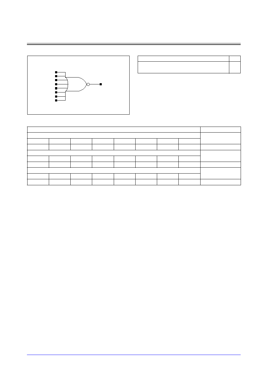
Samsung ASIC
3-65
STDL131
NR8_LP/NR8D2_LP/NR8D4_LP
8-Input NOR with 1X/2X/4X Drive
Logic Symbol
Cell Data
Input Load (SL)
Gate Count
NR8_LP
NR8_LP
A
B
C
D
E
F
G
H
0.9
0.9
0.9
0.9
0.9
0.9
1.0
1.0
5.00
NR8D2_LP
NR8D2_LP
A
B
C
D
E
F
G
H
0.9
0.9
0.9
0.9
0.9
0.9
1.0
1.0
5.33
NR8D4_LP
NR8D4_LP
A
B
C
D
E
F
G
H
0.9
0.9
0.9
0.9
0.9
0.9
1.0
1.0
6.00
Y
C
D
E
F
B
G
A
H
Truth Table
A
B
C
D
E
F
G
H
Y
0
0
0
0
0
0
0
0
1
Other States
0

STDL131
3-66
Samsung ASIC
NR8_LP/NR8D2_LP/NR8D4_LP
8-Input NOR with 1X/2X/4X Drive
Switching Characteristics
(Typical process, 25
∞
C, 1.8V, t
R
/t
F
= 0.19ns, SL: Standard Load)
NR8_LP
Path
Parameter
Delay [ns]
SL = 2
Delay Equations [ns]
Group1*
Group2*
Group3*
A to Y
tR
0.109
0.059 + 0.025*SL
0.058 + 0.025*SL
0.051 + 0.026*SL
tF
0.079
0.046 + 0.016*SL
0.046 + 0.016*SL
0.044 + 0.017*SL
tPLH
0.322
0.292 + 0.015*SL
0.299 + 0.013*SL
0.303 + 0.013*SL
tPHL
0.238
0.213 + 0.013*SL
0.222 + 0.010*SL
0.228 + 0.010*SL
B to Y
tR
0.109
0.059 + 0.025*SL
0.057 + 0.025*SL
0.051 + 0.026*SL
tF
0.078
0.045 + 0.017*SL
0.046 + 0.016*SL
0.044 + 0.017*SL
tPLH
0.369
0.339 + 0.015*SL
0.347 + 0.013*SL
0.351 + 0.013*SL
tPHL
0.258
0.233 + 0.012*SL
0.241 + 0.010*SL
0.247 + 0.010*SL
C to Y
tR
0.109
0.059 + 0.025*SL
0.057 + 0.025*SL
0.051 + 0.026*SL
tF
0.079
0.046 + 0.017*SL
0.047 + 0.016*SL
0.045 + 0.017*SL
tPLH
0.389
0.358 + 0.015*SL
0.366 + 0.013*SL
0.370 + 0.013*SL
tPHL
0.268
0.243 + 0.013*SL
0.252 + 0.010*SL
0.258 + 0.010*SL
D to Y
tR
0.109
0.059 + 0.025*SL
0.058 + 0.025*SL
0.051 + 0.026*SL
tF
0.081
0.048 + 0.016*SL
0.048 + 0.016*SL
0.046 + 0.017*SL
tPLH
0.322
0.292 + 0.015*SL
0.300 + 0.013*SL
0.304 + 0.013*SL
tPHL
0.252
0.227 + 0.013*SL
0.235 + 0.010*SL
0.242 + 0.010*SL
E to Y
tR
0.109
0.059 + 0.025*SL
0.058 + 0.025*SL
0.051 + 0.026*SL
tF
0.080
0.046 + 0.017*SL
0.051 + 0.016*SL
0.044 + 0.017*SL
tPLH
0.368
0.338 + 0.015*SL
0.346 + 0.013*SL
0.350 + 0.013*SL
tPHL
0.271
0.245 + 0.013*SL
0.254 + 0.011*SL
0.261 + 0.010*SL
F to Y
tR
0.109
0.060 + 0.025*SL
0.058 + 0.025*SL
0.051 + 0.026*SL
tF
0.082
0.050 + 0.016*SL
0.048 + 0.016*SL
0.047 + 0.016*SL
tPLH
0.386
0.356 + 0.015*SL
0.364 + 0.013*SL
0.368 + 0.013*SL
tPHL
0.282
0.256 + 0.013*SL
0.265 + 0.011*SL
0.272 + 0.010*SL
G to Y
tR
0.107
0.058 + 0.025*SL
0.056 + 0.025*SL
0.049 + 0.026*SL
tF
0.083
0.050 + 0.017*SL
0.053 + 0.016*SL
0.047 + 0.017*SL
tPLH
0.292
0.262 + 0.015*SL
0.270 + 0.013*SL
0.274 + 0.013*SL
tPHL
0.235
0.209 + 0.013*SL
0.218 + 0.011*SL
0.225 + 0.010*SL
H to Y
tR
0.106
0.057 + 0.025*SL
0.054 + 0.026*SL
0.049 + 0.026*SL
tF
0.084
0.052 + 0.016*SL
0.050 + 0.016*SL
0.049 + 0.016*SL
tPLH
0.311
0.281 + 0.015*SL
0.289 + 0.013*SL
0.293 + 0.013*SL
tPHL
0.249
0.224 + 0.013*SL
0.233 + 0.011*SL
0.240 + 0.010*SL
*Group1 : SL < 4, *Group2 : 4 SL
<
<
=
= 8, *Group3 : 8 < SL

Samsung ASIC
3-67
STDL131
NR8_LP/NR8D2_LP/NR8D4_LP
8-Input NOR with 1X/2X/4X Drive
Switching Characteristics
(Typical process, 25
∞
C, 1.8V, t
R
/t
F
= 0.19ns, SL: Standard Load)
NR8D2_LP
Path
Parameter
Delay [ns]
SL = 2
Delay Equations [ns]
Group1*
Group2*
Group3*
A to Y
tR
0.087
0.062 + 0.012*SL
0.062 + 0.012*SL
0.058 + 0.013*SL
tF
0.070
0.051 + 0.010*SL
0.057 + 0.008*SL
0.058 + 0.008*SL
tPLH
0.332
0.312 + 0.010*SL
0.322 + 0.007*SL
0.333 + 0.006*SL
tPHL
0.259
0.241 + 0.009*SL
0.251 + 0.006*SL
0.265 + 0.005*SL
B to Y
tR
0.087
0.062 + 0.013*SL
0.063 + 0.012*SL
0.058 + 0.013*SL
tF
0.071
0.052 + 0.010*SL
0.058 + 0.008*SL
0.057 + 0.008*SL
tPLH
0.380
0.360 + 0.010*SL
0.369 + 0.007*SL
0.381 + 0.006*SL
tPHL
0.278
0.261 + 0.009*SL
0.271 + 0.006*SL
0.285 + 0.005*SL
C to Y
tR
0.086
0.060 + 0.013*SL
0.064 + 0.012*SL
0.058 + 0.013*SL
tF
0.071
0.052 + 0.010*SL
0.058 + 0.008*SL
0.058 + 0.008*SL
tPLH
0.399
0.379 + 0.010*SL
0.389 + 0.007*SL
0.400 + 0.006*SL
tPHL
0.289
0.271 + 0.009*SL
0.281 + 0.006*SL
0.296 + 0.005*SL
D to Y
tR
0.086
0.058 + 0.014*SL
0.064 + 0.012*SL
0.058 + 0.013*SL
tF
0.073
0.053 + 0.010*SL
0.059 + 0.008*SL
0.061 + 0.008*SL
tPLH
0.329
0.310 + 0.010*SL
0.319 + 0.007*SL
0.331 + 0.006*SL
tPHL
0.273
0.255 + 0.009*SL
0.265 + 0.006*SL
0.280 + 0.005*SL
E to Y
tR
0.085
0.057 + 0.014*SL
0.064 + 0.012*SL
0.058 + 0.013*SL
tF
0.074
0.054 + 0.010*SL
0.060 + 0.008*SL
0.060 + 0.008*SL
tPLH
0.376
0.356 + 0.010*SL
0.366 + 0.007*SL
0.378 + 0.006*SL
tPHL
0.292
0.274 + 0.009*SL
0.284 + 0.006*SL
0.299 + 0.005*SL
F to Y
tR
0.086
0.061 + 0.013*SL
0.062 + 0.012*SL
0.058 + 0.013*SL
tF
0.074
0.055 + 0.009*SL
0.061 + 0.008*SL
0.060 + 0.008*SL
tPLH
0.394
0.374 + 0.010*SL
0.384 + 0.007*SL
0.396 + 0.006*SL
tPHL
0.304
0.286 + 0.009*SL
0.296 + 0.006*SL
0.311 + 0.005*SL
G to Y
tR
0.084
0.056 + 0.014*SL
0.062 + 0.012*SL
0.056 + 0.013*SL
tF
0.075
0.056 + 0.009*SL
0.062 + 0.008*SL
0.061 + 0.008*SL
tPLH
0.296
0.277 + 0.010*SL
0.286 + 0.007*SL
0.298 + 0.006*SL
tPHL
0.253
0.235 + 0.009*SL
0.246 + 0.006*SL
0.261 + 0.005*SL
H to Y
tR
0.085
0.059 + 0.013*SL
0.061 + 0.012*SL
0.056 + 0.013*SL
tF
0.075
0.057 + 0.009*SL
0.062 + 0.008*SL
0.061 + 0.008*SL
tPLH
0.316
0.297 + 0.010*SL
0.306 + 0.007*SL
0.318 + 0.006*SL
tPHL
0.268
0.250 + 0.009*SL
0.261 + 0.006*SL
0.276 + 0.005*SL
*Group1 : SL < 4, *Group2 : 4 SL
<
<
=
= 12, *Group3 : 12 < SL

STDL131
3-68
Samsung ASIC
NR8_LP/NR8D2_LP/NR8D4_LP
8-Input NOR with 1X/2X/4X Drive
Switching Characteristics
(Typical process, 25
∞
C, 1.8V, t
R
/t
F
= 0.19ns, SL: Standard Load)
NR8D4_LP
Path
Parameter
Delay [ns]
SL = 2
Delay Equations [ns]
Group1*
Group2*
Group3*
A to Y
tR
0.090
0.074 + 0.008*SL
0.080 + 0.006*SL
0.084 + 0.006*SL
tF
0.079
0.067 + 0.006*SL
0.074 + 0.004*SL
0.082 + 0.004*SL
tPLH
0.385
0.371 + 0.007*SL
0.379 + 0.005*SL
0.402 + 0.003*SL
tPHL
0.304
0.292 + 0.006*SL
0.300 + 0.004*SL
0.324 + 0.003*SL
B to Y
tR
0.089
0.073 + 0.008*SL
0.080 + 0.006*SL
0.084 + 0.006*SL
tF
0.079
0.067 + 0.006*SL
0.074 + 0.004*SL
0.082 + 0.004*SL
tPLH
0.432
0.419 + 0.007*SL
0.427 + 0.005*SL
0.450 + 0.003*SL
tPHL
0.324
0.312 + 0.006*SL
0.320 + 0.004*SL
0.344 + 0.003*SL
C to Y
tR
0.090
0.074 + 0.008*SL
0.080 + 0.006*SL
0.084 + 0.006*SL
tF
0.080
0.068 + 0.006*SL
0.075 + 0.004*SL
0.084 + 0.004*SL
tPLH
0.451
0.438 + 0.007*SL
0.446 + 0.005*SL
0.469 + 0.003*SL
tPHL
0.335
0.323 + 0.006*SL
0.331 + 0.004*SL
0.355 + 0.003*SL
D to Y
tR
0.090
0.074 + 0.008*SL
0.080 + 0.006*SL
0.084 + 0.006*SL
tF
0.083
0.071 + 0.006*SL
0.077 + 0.004*SL
0.086 + 0.004*SL
tPLH
0.377
0.363 + 0.007*SL
0.371 + 0.005*SL
0.394 + 0.003*SL
tPHL
0.315
0.303 + 0.006*SL
0.312 + 0.004*SL
0.336 + 0.003*SL
E to Y
tR
0.090
0.074 + 0.008*SL
0.080 + 0.006*SL
0.084 + 0.006*SL
tF
0.083
0.070 + 0.006*SL
0.078 + 0.004*SL
0.086 + 0.004*SL
tPLH
0.423
0.410 + 0.007*SL
0.418 + 0.005*SL
0.440 + 0.003*SL
tPHL
0.334
0.322 + 0.006*SL
0.331 + 0.004*SL
0.355 + 0.003*SL
F to Y
tR
0.089
0.072 + 0.008*SL
0.080 + 0.006*SL
0.084 + 0.006*SL
tF
0.083
0.071 + 0.006*SL
0.077 + 0.004*SL
0.086 + 0.004*SL
tPLH
0.441
0.428 + 0.007*SL
0.436 + 0.005*SL
0.458 + 0.003*SL
tPHL
0.346
0.334 + 0.006*SL
0.343 + 0.004*SL
0.367 + 0.003*SL
G to Y
tR
0.090
0.075 + 0.007*SL
0.078 + 0.006*SL
0.082 + 0.006*SL
tF
0.084
0.072 + 0.006*SL
0.079 + 0.004*SL
0.087 + 0.004*SL
tPLH
0.345
0.332 + 0.006*SL
0.340 + 0.005*SL
0.362 + 0.003*SL
tPHL
0.296
0.283 + 0.006*SL
0.292 + 0.004*SL
0.317 + 0.003*SL
H to Y
tR
0.087
0.070 + 0.008*SL
0.078 + 0.006*SL
0.082 + 0.006*SL
tF
0.085
0.072 + 0.006*SL
0.080 + 0.004*SL
0.088 + 0.004*SL
tPLH
0.364
0.350 + 0.007*SL
0.359 + 0.005*SL
0.381 + 0.003*SL
tPHL
0.310
0.298 + 0.006*SL
0.307 + 0.004*SL
0.331 + 0.003*SL
*Group1 : SL < 4, *Group2 : 4 SL
<
<
=
= 20, *Group3 : 20 < SL

Samsung ASIC
3-69
STDL131
OR2_LP/OR2D2_LP/OR2D4_LP/OR2D8_LP
2-Input OR with 1X/2X/4X/8X Drive
Logic Symbol
Cell Data
Switching Characteristics
(Typical process, 25
∞
C, 1.8V, t
R
/t
F
= 0.19ns, SL: Standard Load)
OR2_LP
OR2D2_LP
Input Load (SL)
Gate Count
OR2_LP
OR2D2_LP OR2D4_LP OR2D8_LP
OR2_LP
OR2D2_LP OR2D4_LP OR2D8_LP
A
B
A
B
A
B
A
B
0.8
0.8
1.1
1.1
1.0
1.1
2.0
2.1
1.33
1.67
2.33
4.33
Y
A
B
Path
Parameter
Delay [ns]
SL = 2
Delay Equations [ns]
Group1*
Group2*
Group3*
A to Y
tR
0.092
0.043 + 0.025*SL
0.037 + 0.026*SL
0.033 + 0.027*SL
tF
0.088
0.052 + 0.018*SL
0.056 + 0.017*SL
0.056 + 0.017*SL
tPLH
0.143
0.117 + 0.013*SL
0.119 + 0.013*SL
0.120 + 0.013*SL
tPHL
0.206
0.178 + 0.014*SL
0.189 + 0.011*SL
0.198 + 0.010*SL
B to Y
tR
0.092
0.041 + 0.026*SL
0.040 + 0.026*SL
0.034 + 0.027*SL
tF
0.089
0.053 + 0.018*SL
0.059 + 0.017*SL
0.057 + 0.017*SL
tPLH
0.158
0.131 + 0.013*SL
0.133 + 0.013*SL
0.135 + 0.013*SL
tPHL
0.226
0.197 + 0.014*SL
0.208 + 0.011*SL
0.218 + 0.010*SL
*Group1 : SL < 4, *Group2 : 4 SL
<
<
=
= 8, *Group3 : 8 < SL
Path
Parameter
Delay [ns]
SL = 2
Delay Equations [ns]
Group1*
Group2*
Group3*
A to Y
tR
0.064
0.041 + 0.012*SL
0.037 + 0.013*SL
0.029 + 0.013*SL
tF
0.072
0.053 + 0.010*SL
0.058 + 0.008*SL
0.059 + 0.008*SL
tPLH
0.128
0.113 + 0.007*SL
0.117 + 0.006*SL
0.119 + 0.006*SL
tPHL
0.203
0.185 + 0.009*SL
0.195 + 0.007*SL
0.210 + 0.005*SL
B to Y
tR
0.067
0.046 + 0.010*SL
0.035 + 0.013*SL
0.031 + 0.013*SL
tF
0.071
0.051 + 0.010*SL
0.057 + 0.009*SL
0.061 + 0.008*SL
tPLH
0.141
0.126 + 0.007*SL
0.130 + 0.006*SL
0.132 + 0.006*SL
tPHL
0.223
0.205 + 0.009*SL
0.215 + 0.007*SL
0.230 + 0.005*SL
*Group1 : SL < 4, *Group2 : 4 SL
<
<
=
= 12, *Group3 : 12 < SL
Truth Table
A
B
Y
0
0
0
0
1
1
1
0
1
1
1
1

STDL131
3-70
Samsung ASIC
OR2_LP/OR2D2_LP/OR2D4_LP/OR2D8_LP
2-Input OR with 1X/2X/4X/8X Drive
Switching Characteristics
(Typical process, 25
∞
C, 1.8V, t
R
/t
F
= 0.19ns, SL: Standard Load)
OR2D4_LP
OR2D8_LP
Path
Parameter
Delay [ns]
SL = 2
Delay Equations [ns]
Group1*
Group2*
Group3*
A to Y
tR
0.064
0.052 + 0.006*SL
0.052 + 0.006*SL
0.045 + 0.006*SL
tF
0.084
0.071 + 0.006*SL
0.078 + 0.005*SL
0.090 + 0.004*SL
tPLH
0.164
0.154 + 0.005*SL
0.159 + 0.004*SL
0.168 + 0.003*SL
tPHL
0.260
0.247 + 0.006*SL
0.256 + 0.004*SL
0.281 + 0.003*SL
B to Y
tR
0.065
0.053 + 0.006*SL
0.052 + 0.006*SL
0.045 + 0.006*SL
tF
0.085
0.072 + 0.007*SL
0.080 + 0.005*SL
0.088 + 0.004*SL
tPLH
0.177
0.167 + 0.005*SL
0.172 + 0.004*SL
0.182 + 0.003*SL
tPHL
0.280
0.267 + 0.006*SL
0.276 + 0.004*SL
0.301 + 0.003*SL
*Group1 : SL < 4, *Group2 : 4 SL
<
<
=
= 20, *Group3 : 20 < SL
Path
Parameter
Delay [ns]
SL = 2
Delay Equations [ns]
Group1*
Group2*
Group3*
A to Y
tR
0.056
0.051 + 0.003*SL
0.048 + 0.003*SL
0.044 + 0.003*SL
tF
0.077
0.071 + 0.003*SL
0.073 + 0.002*SL
0.088 + 0.002*SL
tPLH
0.156
0.150 + 0.003*SL
0.154 + 0.002*SL
0.164 + 0.002*SL
tPHL
0.247
0.240 + 0.003*SL
0.245 + 0.002*SL
0.273 + 0.001*SL
B to Y
tR
0.058
0.052 + 0.003*SL
0.053 + 0.003*SL
0.045 + 0.003*SL
tF
0.076
0.068 + 0.004*SL
0.074 + 0.002*SL
0.086 + 0.002*SL
tPLH
0.170
0.165 + 0.003*SL
0.168 + 0.002*SL
0.180 + 0.002*SL
tPHL
0.268
0.261 + 0.003*SL
0.266 + 0.002*SL
0.293 + 0.001*SL
*Group1 : SL < 4, *Group2 : 4 SL
<
<
=
= 37, *Group3 : 37 < SL

Samsung ASIC
3-71
STDL131
OR2B_LP/OR2BD2_LP/OR2BD4_LP/OR2BD8_LP
2-Input OR with one Inverted Input, 1X/2X/4X/8X Drive
Logic Symbol
Cell Data
Switching Characteristics
(Typical process, 25
∞
C, 1.8V, t
R
/t
F
= 0.19ns, SL: Standard Load)
OR2B_LP
OR2BD2_LP
Input Load (SL)
Gate Count
OR2B_LP OR2BD2_LP OR2BD4_LP OR2BD8_LP OR2B_LP OR2BD2_LP OR2BD4_LP OR2BD8_LP
AN
B
AN
B
AN
B
AN
B
0.5
0.8
0.6
1.1
0.6
1.1
0.8
2.3
2.00
2.00
2.67
4.67
Truth Table
AN
B
Y
0
0
1
0
1
1
1
0
0
1
1
1
Y
AN
B
Path
Parameter
Delay [ns]
SL = 2
Delay Equations [ns]
Group1*
Group2*
Group3*
AN to Y
tR
0.092
0.042 + 0.025*SL
0.038 + 0.026*SL
0.033 + 0.027*SL
tF
0.088
0.052 + 0.018*SL
0.058 + 0.016*SL
0.058 + 0.016*SL
tPLH
0.230
0.204 + 0.013*SL
0.206 + 0.013*SL
0.207 + 0.013*SL
tPHL
0.245
0.216 + 0.014*SL
0.228 + 0.011*SL
0.237 + 0.010*SL
B to Y
tR
0.093
0.042 + 0.025*SL
0.040 + 0.026*SL
0.035 + 0.027*SL
tF
0.089
0.053 + 0.018*SL
0.059 + 0.016*SL
0.057 + 0.016*SL
tPLH
0.158
0.132 + 0.013*SL
0.134 + 0.013*SL
0.135 + 0.013*SL
tPHL
0.227
0.199 + 0.014*SL
0.210 + 0.011*SL
0.220 + 0.010*SL
*Group1 : SL < 4, *Group2 : 4 SL
<
<
=
= 8, *Group3 : 8 < SL
Path
Parameter
Delay [ns]
SL = 2
Delay Equations [ns]
Group1*
Group2*
Group3*
AN to Y
tR
0.062
0.037 + 0.012*SL
0.035 + 0.013*SL
0.029 + 0.013*SL
tF
0.071
0.051 + 0.010*SL
0.057 + 0.009*SL
0.062 + 0.008*SL
tPLH
0.224
0.209 + 0.007*SL
0.213 + 0.006*SL
0.215 + 0.006*SL
tPHL
0.246
0.227 + 0.009*SL
0.238 + 0.007*SL
0.253 + 0.005*SL
B to Y
tR
0.063
0.039 + 0.012*SL
0.035 + 0.013*SL
0.030 + 0.013*SL
tF
0.072
0.051 + 0.010*SL
0.058 + 0.009*SL
0.062 + 0.008*SL
tPLH
0.136
0.122 + 0.007*SL
0.125 + 0.006*SL
0.127 + 0.006*SL
tPHL
0.226
0.207 + 0.009*SL
0.218 + 0.007*SL
0.233 + 0.005*SL
*Group1 : SL < 4, *Group2 : 4 SL
<
<
=
= 12, *Group3 : 12 < SL
STDL131
3-72
Samsung ASIC
OR2B_LP/OR2BD2_LP/OR2BD4_LP/OR2BD8_LP
2-Input OR with one Inverted Input, 1X/2X/4X/8X Drive
Switching Characteristics
(Typical process, 25
∞
C, 1.8V, t
R
/t
F
= 0.19ns, SL: Standard Load)
OR2BD4_LP
OR2BD8_LP
Path
Parameter
Delay [ns]
SL = 2
Delay Equations [ns]
Group1*
Group2*
Group3*
AN to Y
tR
0.060
0.049 + 0.006*SL
0.048 + 0.006*SL
0.039 + 0.007*SL
tF
0.086
0.073 + 0.007*SL
0.081 + 0.005*SL
0.090 + 0.004*SL
tPLH
0.247
0.238 + 0.005*SL
0.242 + 0.004*SL
0.250 + 0.003*SL
tPHL
0.306
0.293 + 0.007*SL
0.303 + 0.004*SL
0.328 + 0.003*SL
B to Y
tR
0.060
0.049 + 0.005*SL
0.047 + 0.006*SL
0.039 + 0.007*SL
tF
0.086
0.073 + 0.007*SL
0.081 + 0.005*SL
0.091 + 0.004*SL
tPLH
0.156
0.147 + 0.005*SL
0.151 + 0.004*SL
0.158 + 0.003*SL
tPHL
0.285
0.272 + 0.007*SL
0.282 + 0.004*SL
0.307 + 0.003*SL
*Group1 : SL < 4, *Group2 : 4 SL
<
<
=
= 20, *Group3 : 20 < SL
Path
Parameter
Delay [ns]
SL = 2
Delay Equations [ns]
Group1*
Group2*
Group3*
AN to Y
tR
0.052
0.045 + 0.003*SL
0.046 + 0.003*SL
0.040 + 0.003*SL
tF
0.078
0.071 + 0.004*SL
0.075 + 0.002*SL
0.088 + 0.002*SL
tPLH
0.250
0.245 + 0.003*SL
0.248 + 0.002*SL
0.257 + 0.002*SL
tPHL
0.314
0.307 + 0.003*SL
0.311 + 0.002*SL
0.339 + 0.001*SL
B to Y
tR
0.053
0.045 + 0.004*SL
0.047 + 0.003*SL
0.040 + 0.003*SL
tF
0.077
0.070 + 0.004*SL
0.075 + 0.002*SL
0.087 + 0.002*SL
tPLH
0.148
0.143 + 0.003*SL
0.146 + 0.002*SL
0.155 + 0.002*SL
tPHL
0.274
0.267 + 0.003*SL
0.272 + 0.002*SL
0.300 + 0.001*SL
*Group1 : SL < 4, *Group2 : 4 SL
<
<
=
= 37, *Group3 : 37 < SL
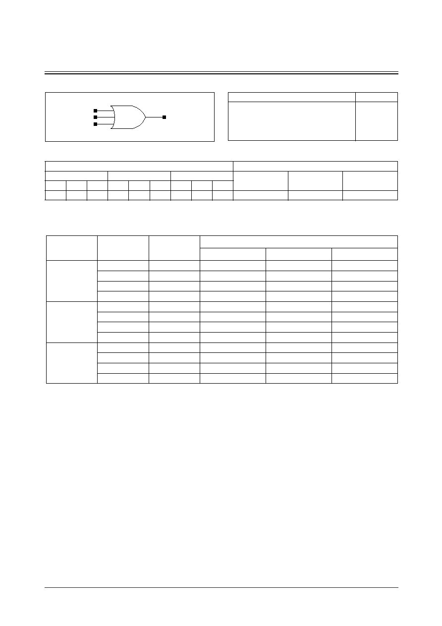
Samsung ASIC
3-73
STDL131
OR3_LP/OR3D2_LP/OR3D4_LP
3-Input OR with 1X/2X/4X Drive
Logic Symbol
Cell Data
Switching Characteristics
(Typical process, 25
∞
C, 1.8V, t
R
/t
F
= 0.19ns, SL: Standard Load)
OR3_LP
Input Load (SL)
Gate Count
OR3_LP
OR3D2_LP
OR3D4_LP
OR3_LP
OR3D2_LP
OR3D4_LP
A
B
C
A
B
C
A
B
C
0.7
0.8
0.8
1.1
1.1
1.1
1.0
1.0
1.0
1.67
2.33
2.67
Y
A
B
C
Path
Parameter
Delay [ns]
SL = 2
Delay Equations [ns]
Group1*
Group2*
Group3*
A to Y
tR
0.095
0.045 + 0.025*SL
0.040 + 0.026*SL
0.038 + 0.026*SL
tF
0.112
0.073 + 0.020*SL
0.081 + 0.018*SL
0.087 + 0.017*SL
tPLH
0.156
0.130 + 0.013*SL
0.133 + 0.013*SL
0.134 + 0.012*SL
tPHL
0.258
0.224 + 0.017*SL
0.239 + 0.013*SL
0.254 + 0.011*SL
B to Y
tR
0.097
0.049 + 0.024*SL
0.041 + 0.026*SL
0.040 + 0.026*SL
tF
0.112
0.073 + 0.020*SL
0.082 + 0.017*SL
0.088 + 0.017*SL
tPLH
0.172
0.145 + 0.014*SL
0.149 + 0.013*SL
0.150 + 0.012*SL
tPHL
0.306
0.272 + 0.017*SL
0.286 + 0.013*SL
0.302 + 0.011*SL
C to Y
tR
0.100
0.050 + 0.025*SL
0.047 + 0.026*SL
0.043 + 0.026*SL
tF
0.112
0.071 + 0.020*SL
0.083 + 0.017*SL
0.088 + 0.017*SL
tPLH
0.181
0.153 + 0.014*SL
0.158 + 0.013*SL
0.159 + 0.013*SL
tPHL
0.325
0.291 + 0.017*SL
0.305 + 0.013*SL
0.321 + 0.011*SL
*Group1 : SL < 4, *Group2 : 4 SL
<
<
=
= 8, *Group3 : 8 < SL
Truth Table
A
B
C
Y
0
0
0
0
1
x
x
1
x
1
x
1
x
x
1
1

STDL131
3-74
Samsung ASIC
OR3_LP/OR3D2_LP/OR3D4_LP
3-Input OR with 1X/2X/4X Drive
Switching Characteristics
(Typical process, 25
∞
C, 1.8V, t
R
/t
F
= 0.19ns, SL: Standard Load)
OR3D2_LP
OR3D4_LP
Path
Parameter
Delay [ns]
SL = 2
Delay Equations [ns]
Group1*
Group2*
Group3*
A to Y
tR
0.066
0.043 + 0.011*SL
0.038 + 0.013*SL
0.032 + 0.013*SL
tF
0.095
0.072 + 0.011*SL
0.079 + 0.009*SL
0.090 + 0.009*SL
tPLH
0.139
0.124 + 0.007*SL
0.128 + 0.006*SL
0.131 + 0.006*SL
tPHL
0.259
0.237 + 0.011*SL
0.250 + 0.008*SL
0.272 + 0.006*SL
B to Y
tR
0.070
0.048 + 0.011*SL
0.042 + 0.012*SL
0.034 + 0.013*SL
tF
0.094
0.072 + 0.011*SL
0.078 + 0.010*SL
0.091 + 0.009*SL
tPLH
0.152
0.137 + 0.008*SL
0.142 + 0.007*SL
0.145 + 0.006*SL
tPHL
0.309
0.287 + 0.011*SL
0.299 + 0.008*SL
0.321 + 0.006*SL
C to Y
tR
0.069
0.044 + 0.013*SL
0.044 + 0.013*SL
0.039 + 0.013*SL
tF
0.094
0.072 + 0.011*SL
0.078 + 0.010*SL
0.091 + 0.009*SL
tPLH
0.160
0.144 + 0.008*SL
0.149 + 0.007*SL
0.153 + 0.006*SL
tPHL
0.329
0.307 + 0.011*SL
0.320 + 0.008*SL
0.341 + 0.006*SL
*Group1 : SL < 4, *Group2 : 4 SL
<
<
=
= 12, *Group3 : 12 < SL
Path
Parameter
Delay [ns]
SL = 2
Delay Equations [ns]
Group1*
Group2*
Group3*
A to Y
tR
0.069
0.056 + 0.006*SL
0.057 + 0.006*SL
0.051 + 0.006*SL
tF
0.112
0.098 + 0.007*SL
0.106 + 0.005*SL
0.125 + 0.004*SL
tPLH
0.182
0.172 + 0.005*SL
0.178 + 0.004*SL
0.190 + 0.003*SL
tPHL
0.340
0.325 + 0.007*SL
0.334 + 0.005*SL
0.367 + 0.003*SL
B to Y
tR
0.072
0.060 + 0.006*SL
0.060 + 0.006*SL
0.052 + 0.006*SL
tF
0.114
0.100 + 0.007*SL
0.106 + 0.005*SL
0.126 + 0.004*SL
tPLH
0.199
0.189 + 0.005*SL
0.195 + 0.004*SL
0.207 + 0.003*SL
tPHL
0.387
0.372 + 0.007*SL
0.381 + 0.005*SL
0.414 + 0.003*SL
C to Y
tR
0.076
0.063 + 0.007*SL
0.065 + 0.006*SL
0.058 + 0.006*SL
tF
0.114
0.100 + 0.007*SL
0.105 + 0.005*SL
0.127 + 0.004*SL
tPLH
0.209
0.198 + 0.006*SL
0.205 + 0.004*SL
0.219 + 0.003*SL
tPHL
0.405
0.390 + 0.007*SL
0.399 + 0.005*SL
0.432 + 0.003*SL
*Group1 : SL < 4, *Group2 : 4 SL
<
<
=
= 20, *Group3 : 20 < SL

Samsung ASIC
3-75
STDL131
OR4_LP/OR4D2_LP/OR4D4_LP
4-Input OR with 1X/2X/4X Drive
Logic Symbol
Cell Data
Switching Characteristics
(Typical process, 25
∞
C, 1.8V, t
R
/t
F
= 0.19ns, SL: Standard Load)
OR4_LP
Input Load (SL)
OR4_LP
OR4D2_LP
OR4D4_LP
A
B
C
D
A
B
C
D
A
B
C
D
0.8
0.8
0.8
0.8
1.0
1.1
1.0
1.0
0.8
0.8
0.8
0.8
Gate Count
OR4_LP
OR4D2_LP
OR4D4_LP
2.67
3.00
4.67
Y
A
B
C
D
Path
Parameter
Delay [ns]
SL = 2
Delay Equations [ns]
Group1*
Group2*
Group3*
A to Y
tR
0.104
0.055 + 0.025*SL
0.050 + 0.026*SL
0.047 + 0.026*SL
tF
0.126
0.075 + 0.026*SL
0.076 + 0.025*SL
0.073 + 0.026*SL
tPLH
0.152
0.126 + 0.013*SL
0.128 + 0.013*SL
0.129 + 0.012*SL
tPHL
0.231
0.197 + 0.017*SL
0.205 + 0.015*SL
0.212 + 0.014*SL
B to Y
tR
0.104
0.054 + 0.025*SL
0.051 + 0.026*SL
0.048 + 0.026*SL
tF
0.126
0.076 + 0.025*SL
0.075 + 0.025*SL
0.073 + 0.026*SL
tPLH
0.167
0.140 + 0.013*SL
0.143 + 0.013*SL
0.143 + 0.012*SL
tPHL
0.251
0.217 + 0.017*SL
0.225 + 0.015*SL
0.232 + 0.014*SL
C to Y
tR
0.112
0.063 + 0.025*SL
0.058 + 0.026*SL
0.055 + 0.026*SL
tF
0.119
0.067 + 0.026*SL
0.068 + 0.026*SL
0.065 + 0.026*SL
tPLH
0.159
0.133 + 0.013*SL
0.135 + 0.013*SL
0.136 + 0.012*SL
tPHL
0.232
0.199 + 0.016*SL
0.205 + 0.015*SL
0.210 + 0.014*SL
D to Y
tR
0.114
0.063 + 0.025*SL
0.060 + 0.026*SL
0.057 + 0.026*SL
tF
0.119
0.068 + 0.026*SL
0.067 + 0.026*SL
0.064 + 0.026*SL
tPLH
0.174
0.148 + 0.013*SL
0.149 + 0.013*SL
0.150 + 0.012*SL
tPHL
0.251
0.218 + 0.016*SL
0.224 + 0.015*SL
0.230 + 0.014*SL
*Group1 : SL < 4, *Group2 : 4 SL
<
<
=
= 8, *Group3 : 8 < SL
Truth Table
A
B
C
D
Y
0
0
0
0
0
1
x
x
x
1
x
1
x
x
1
x
x
1
x
1
x
x
x
1
1

STDL131
3-76
Samsung ASIC
OR4_LP/OR4D2_LP/OR4D4_LP
4-Input OR with 1X/2X/4X Drive
Switching Characteristics
(Typical process, 25
∞
C, 1.8V, t
R
/t
F
= 0.19ns, SL: Standard Load)
OR4D2_LP
OR4D4_LP
Path
Parameter
Delay [ns]
SL = 2
Delay Equations [ns]
Group1*
Group2*
Group3*
A to Y
tR
0.081
0.058 + 0.012*SL
0.053 + 0.013*SL
0.048 + 0.013*SL
tF
0.101
0.073 + 0.014*SL
0.078 + 0.013*SL
0.075 + 0.013*SL
tPLH
0.158
0.143 + 0.007*SL
0.146 + 0.007*SL
0.149 + 0.006*SL
tPHL
0.225
0.205 + 0.010*SL
0.212 + 0.008*SL
0.223 + 0.007*SL
B to Y
tR
0.083
0.058 + 0.012*SL
0.057 + 0.013*SL
0.050 + 0.013*SL
tF
0.101
0.076 + 0.013*SL
0.075 + 0.013*SL
0.075 + 0.013*SL
tPLH
0.175
0.160 + 0.008*SL
0.164 + 0.007*SL
0.167 + 0.006*SL
tPHL
0.245
0.224 + 0.010*SL
0.232 + 0.008*SL
0.243 + 0.007*SL
C to Y
tR
0.089
0.063 + 0.013*SL
0.064 + 0.013*SL
0.056 + 0.013*SL
tF
0.092
0.065 + 0.014*SL
0.067 + 0.013*SL
0.066 + 0.013*SL
tPLH
0.167
0.153 + 0.007*SL
0.155 + 0.007*SL
0.158 + 0.006*SL
tPHL
0.227
0.208 + 0.009*SL
0.213 + 0.008*SL
0.222 + 0.007*SL
D to Y
tR
0.090
0.067 + 0.012*SL
0.062 + 0.013*SL
0.059 + 0.013*SL
tF
0.092
0.063 + 0.014*SL
0.068 + 0.013*SL
0.066 + 0.013*SL
tPLH
0.184
0.170 + 0.007*SL
0.173 + 0.007*SL
0.175 + 0.006*SL
tPHL
0.246
0.227 + 0.009*SL
0.232 + 0.008*SL
0.241 + 0.007*SL
*Group1 : SL < 4, *Group2 : 4 SL
<
<
=
= 12, *Group3 : 12 < SL
Path
Parameter
Delay [ns]
SL = 2
Delay Equations [ns]
Group1*
Group2*
Group3*
A to Y
tR
0.061
0.047 + 0.007*SL
0.051 + 0.006*SL
0.042 + 0.007*SL
tF
0.056
0.046 + 0.005*SL
0.048 + 0.004*SL
0.050 + 0.004*SL
tPLH
0.296
0.287 + 0.005*SL
0.292 + 0.004*SL
0.300 + 0.003*SL
tPHL
0.356
0.346 + 0.005*SL
0.352 + 0.003*SL
0.366 + 0.003*SL
B to Y
tR
0.062
0.051 + 0.006*SL
0.049 + 0.006*SL
0.040 + 0.007*SL
tF
0.056
0.045 + 0.005*SL
0.050 + 0.004*SL
0.050 + 0.004*SL
tPLH
0.313
0.304 + 0.005*SL
0.309 + 0.004*SL
0.317 + 0.003*SL
tPHL
0.376
0.366 + 0.005*SL
0.372 + 0.003*SL
0.386 + 0.003*SL
C to Y
tR
0.063
0.052 + 0.006*SL
0.050 + 0.006*SL
0.040 + 0.007*SL
tF
0.056
0.046 + 0.005*SL
0.049 + 0.004*SL
0.050 + 0.004*SL
tPLH
0.306
0.297 + 0.005*SL
0.302 + 0.004*SL
0.310 + 0.003*SL
tPHL
0.356
0.346 + 0.005*SL
0.352 + 0.003*SL
0.366 + 0.003*SL
D to Y
tR
0.063
0.052 + 0.006*SL
0.050 + 0.006*SL
0.040 + 0.007*SL
tF
0.055
0.045 + 0.005*SL
0.048 + 0.004*SL
0.048 + 0.004*SL
tPLH
0.322
0.312 + 0.005*SL
0.318 + 0.004*SL
0.325 + 0.003*SL
tPHL
0.375
0.365 + 0.005*SL
0.371 + 0.003*SL
0.385 + 0.003*SL
*Group1 : SL < 4, *Group2 : 4 SL
<
<
=
= 20, *Group3 : 20 < SL

Samsung ASIC
3-77
STDL131
OR5_LP/OR5D2_LP/OR5D4_LP
5-Input OR with 1X/2X/4X Drive
Logic Symbol
Cell Data
Switching Characteristics
(Typical process, 25
∞
C, 1.8V, t
R
/t
F
= 0.19ns, SL: Standard Load)
OR5_LP
Input Load (SL)
OR5_LP
OR5D2_LP
OR5D4_LP
A
B
C
D
E
A
B
C
D
E
A
B
C
D
E
0.9
0.9
0.9
0.8
0.8
1.0
1.1
1.0
1.0
1.0
0.9
0.9
1.0
0.8
0.8
Gate Count
OR5_LP
OR5D2_LP
OR5D4_LP
3.00
3.33
4.67
Y
B
C
D
E
A
Path
Parameter
Delay [ns]
SL = 2
Delay Equations [ns]
Group1*
Group2*
Group3*
A to Y
tR
0.103
0.053 + 0.025*SL
0.050 + 0.026*SL
0.047 + 0.026*SL
tF
0.145
0.091 + 0.027*SL
0.095 + 0.026*SL
0.097 + 0.025*SL
tPLH
0.154
0.128 + 0.013*SL
0.129 + 0.013*SL
0.130 + 0.012*SL
tPHL
0.270
0.231 + 0.020*SL
0.243 + 0.017*SL
0.255 + 0.015*SL
B to Y
tR
0.106
0.056 + 0.025*SL
0.052 + 0.026*SL
0.049 + 0.026*SL
tF
0.145
0.092 + 0.027*SL
0.097 + 0.026*SL
0.098 + 0.025*SL
tPLH
0.170
0.143 + 0.013*SL
0.145 + 0.013*SL
0.147 + 0.012*SL
tPHL
0.319
0.280 + 0.020*SL
0.292 + 0.017*SL
0.305 + 0.015*SL
C to Y
tR
0.108
0.058 + 0.025*SL
0.055 + 0.026*SL
0.052 + 0.026*SL
tF
0.145
0.092 + 0.027*SL
0.097 + 0.026*SL
0.098 + 0.025*SL
tPLH
0.178
0.151 + 0.014*SL
0.154 + 0.013*SL
0.155 + 0.013*SL
tPHL
0.340
0.301 + 0.020*SL
0.313 + 0.017*SL
0.325 + 0.015*SL
D to Y
tR
0.113
0.063 + 0.025*SL
0.058 + 0.026*SL
0.056 + 0.026*SL
tF
0.119
0.068 + 0.026*SL
0.068 + 0.026*SL
0.065 + 0.026*SL
tPLH
0.159
0.134 + 0.013*SL
0.135 + 0.013*SL
0.136 + 0.012*SL
tPHL
0.231
0.199 + 0.016*SL
0.205 + 0.015*SL
0.210 + 0.014*SL
E to Y
tR
0.114
0.064 + 0.025*SL
0.061 + 0.026*SL
0.058 + 0.026*SL
tF
0.119
0.068 + 0.026*SL
0.067 + 0.026*SL
0.065 + 0.026*SL
tPLH
0.174
0.148 + 0.013*SL
0.150 + 0.013*SL
0.151 + 0.012*SL
tPHL
0.251
0.219 + 0.016*SL
0.225 + 0.015*SL
0.230 + 0.014*SL
*Group1 : SL < 4, *Group2 : 4 SL
<
<
=
= 8, *Group3 : 8 < SL
Truth Table
A
B
C
D
E
Y
0
0
0
0
0
0
1
x
x
x
x
1
x
1
x
x
x
1
x
x
1
x
x
1
x
x
x
1
x
1
x
x
x
x
1
1

STDL131
3-78
Samsung ASIC
OR5_LP/OR5D2_LP/OR5D4_LP
5-Input OR with 1X/2X/4X Drive
Switching Characteristics
(Typical process, 25
∞
C, 1.8V, t
R
/t
F
= 0.19ns, SL: Standard Load)
OR5D2_LP
Path
Parameter
Delay [ns]
SL = 2
Delay Equations [ns]
Group1*
Group2*
Group3*
A to Y
tR
0.082
0.058 + 0.012*SL
0.056 + 0.013*SL
0.049 + 0.013*SL
tF
0.125
0.095 + 0.015*SL
0.102 + 0.013*SL
0.105 + 0.013*SL
tPLH
0.161
0.146 + 0.007*SL
0.150 + 0.007*SL
0.153 + 0.006*SL
tPHL
0.283
0.259 + 0.012*SL
0.269 + 0.010*SL
0.288 + 0.008*SL
B to Y
tR
0.082
0.058 + 0.012*SL
0.055 + 0.013*SL
0.051 + 0.013*SL
tF
0.126
0.096 + 0.015*SL
0.101 + 0.013*SL
0.106 + 0.013*SL
tPLH
0.178
0.163 + 0.008*SL
0.167 + 0.007*SL
0.170 + 0.006*SL
tPHL
0.330
0.306 + 0.012*SL
0.316 + 0.010*SL
0.335 + 0.008*SL
C to Y
tR
0.086
0.061 + 0.013*SL
0.061 + 0.013*SL
0.054 + 0.013*SL
tF
0.125
0.096 + 0.015*SL
0.101 + 0.013*SL
0.106 + 0.013*SL
tPLH
0.188
0.172 + 0.008*SL
0.176 + 0.007*SL
0.181 + 0.006*SL
tPHL
0.348
0.324 + 0.012*SL
0.334 + 0.010*SL
0.353 + 0.008*SL
D to Y
tR
0.090
0.064 + 0.013*SL
0.065 + 0.013*SL
0.057 + 0.013*SL
tF
0.094
0.066 + 0.014*SL
0.069 + 0.013*SL
0.068 + 0.013*SL
tPLH
0.168
0.154 + 0.007*SL
0.157 + 0.006*SL
0.159 + 0.006*SL
tPHL
0.230
0.211 + 0.010*SL
0.216 + 0.008*SL
0.225 + 0.007*SL
E to Y
tR
0.092
0.068 + 0.012*SL
0.065 + 0.013*SL
0.059 + 0.013*SL
tF
0.094
0.066 + 0.014*SL
0.069 + 0.013*SL
0.068 + 0.013*SL
tPLH
0.186
0.172 + 0.007*SL
0.174 + 0.007*SL
0.177 + 0.006*SL
tPHL
0.250
0.230 + 0.010*SL
0.236 + 0.008*SL
0.245 + 0.007*SL
*Group1 : SL < 4, *Group2 : 4 SL
<
<
=
= 12, *Group3 : 12 < SL

Samsung ASIC
3-79
STDL131
OR5_LP/OR5D2_LP/OR5D4_LP
5-Input OR with 1X/2X/4X Drive
Switching Characteristics
(Typical process, 25
∞
C, 1.8V, t
R
/t
F
= 0.19ns, SL: Standard Load)
OR5D4_LP
Path
Parameter
Delay [ns]
SL = 2
Delay Equations [ns]
Group1*
Group2*
Group3*
A to Y
tR
0.063
0.051 + 0.006*SL
0.050 + 0.006*SL
0.041 + 0.007*SL
tF
0.056
0.046 + 0.005*SL
0.049 + 0.004*SL
0.051 + 0.004*SL
tPLH
0.299
0.289 + 0.005*SL
0.294 + 0.004*SL
0.302 + 0.003*SL
tPHL
0.390
0.380 + 0.005*SL
0.387 + 0.003*SL
0.401 + 0.003*SL
B to Y
tR
0.061
0.048 + 0.007*SL
0.050 + 0.006*SL
0.043 + 0.006*SL
tF
0.057
0.048 + 0.004*SL
0.048 + 0.004*SL
0.049 + 0.004*SL
tPLH
0.316
0.306 + 0.005*SL
0.311 + 0.004*SL
0.319 + 0.003*SL
tPHL
0.437
0.428 + 0.005*SL
0.434 + 0.003*SL
0.448 + 0.003*SL
C to Y
tR
0.062
0.049 + 0.006*SL
0.050 + 0.006*SL
0.042 + 0.007*SL
tF
0.056
0.046 + 0.005*SL
0.050 + 0.004*SL
0.051 + 0.004*SL
tPLH
0.325
0.316 + 0.005*SL
0.321 + 0.004*SL
0.329 + 0.003*SL
tPHL
0.460
0.450 + 0.005*SL
0.456 + 0.003*SL
0.471 + 0.003*SL
D to Y
tR
0.063
0.051 + 0.006*SL
0.051 + 0.006*SL
0.041 + 0.007*SL
tF
0.056
0.046 + 0.005*SL
0.050 + 0.004*SL
0.051 + 0.004*SL
tPLH
0.306
0.296 + 0.005*SL
0.301 + 0.004*SL
0.309 + 0.003*SL
tPHL
0.352
0.342 + 0.005*SL
0.348 + 0.003*SL
0.363 + 0.003*SL
E to Y
tR
0.063
0.052 + 0.006*SL
0.050 + 0.006*SL
0.041 + 0.007*SL
tF
0.056
0.048 + 0.004*SL
0.048 + 0.004*SL
0.049 + 0.004*SL
tPLH
0.323
0.313 + 0.005*SL
0.318 + 0.004*SL
0.326 + 0.003*SL
tPHL
0.372
0.363 + 0.005*SL
0.369 + 0.003*SL
0.383 + 0.003*SL
*Group1 : SL < 4, *Group2 : 4 SL
<
<
=
= 20, *Group3 : 20 < SL
STDL131
3-80
Samsung ASIC
XN2_LP/XN2D2_LP/XN2D4_LP
2-Input Exclusive-NOR with 1X/2X/4X Drive
Logic Symbol
Cell Data
Switching Characteristics
(Typical process, 25
∞
C, 1.8V, t
R
/t
F
= 0.19ns, SL: Standard Load)
XN2_LP
Input Load (SL)
Gate Count
XN2_LP
XN2D2_LP
XN2D4_LP
XN2_LP
XN2D2_LP
XN2D4_LP
A
B
A
B
A
B
0.9
1.4
0.9
1.5
0.9
1.5
2.67
2.67
3.33
Y
A
B
Path
Parameter
Delay [ns]
SL = 2
Delay Equations [ns]
Group1*
Group2*
Group3*
A to Y
tR
0.103
0.055 + 0.024*SL
0.051 + 0.025*SL
0.046 + 0.026*SL
tF
0.109
0.074 + 0.017*SL
0.079 + 0.016*SL
0.080 + 0.016*SL
tPLH
0.251
0.223 + 0.014*SL
0.228 + 0.013*SL
0.230 + 0.012*SL
tPHL
0.270
0.243 + 0.014*SL
0.248 + 0.012*SL
0.261 + 0.011*SL
B to Y
tR
0.102
0.054 + 0.024*SL
0.049 + 0.025*SL
0.046 + 0.026*SL
tF
0.105
0.069 + 0.018*SL
0.076 + 0.016*SL
0.077 + 0.016*SL
tPLH
0.243
0.215 + 0.014*SL
0.220 + 0.013*SL
0.221 + 0.012*SL
tPHL
0.230
0.199 + 0.016*SL
0.212 + 0.012*SL
0.225 + 0.011*SL
*Group1 : SL < 4, *Group2 : 4 SL
<
<
=
= 8, *Group3 : 8 < SL
Truth Table
A
B
Y
0
0
1
0
1
0
1
0
0
1
1
1
Samsung ASIC
3-81
STDL131
XN2_LP/XN2D2_LP/XN2D4_LP
2-Input Exclusive-NOR with 1X/2X/4X Drive
Switching Characteristics
(Typical process, 25
∞
C, 1.8V, t
R
/t
F
= 0.19ns, SL: Standard Load)
XN2D2_LP
XN2D4_LP
Path
Parameter
Delay [ns]
SL = 2
Delay Equations [ns]
Group1*
Group2*
Group3*
A to Y
tR
0.078
0.052 + 0.013*SL
0.054 + 0.012*SL
0.047 + 0.013*SL
tF
0.099
0.077 + 0.011*SL
0.085 + 0.009*SL
0.092 + 0.008*SL
tPLH
0.261
0.243 + 0.009*SL
0.251 + 0.007*SL
0.259 + 0.006*SL
tPHL
0.296
0.276 + 0.010*SL
0.287 + 0.007*SL
0.305 + 0.005*SL
B to Y
tR
0.078
0.053 + 0.012*SL
0.053 + 0.012*SL
0.046 + 0.013*SL
tF
0.094
0.070 + 0.012*SL
0.082 + 0.009*SL
0.088 + 0.008*SL
tPLH
0.257
0.239 + 0.009*SL
0.247 + 0.007*SL
0.255 + 0.006*SL
tPHL
0.226
0.204 + 0.011*SL
0.218 + 0.008*SL
0.240 + 0.006*SL
*Group1 : SL < 4, *Group2 : 4 SL
<
<
=
= 12, *Group3 : 12 < SL
Path
Parameter
Delay [ns]
SL = 2
Delay Equations [ns]
Group1*
Group2*
Group3*
A to Y
tR
0.080
0.065 + 0.007*SL
0.069 + 0.006*SL
0.068 + 0.006*SL
tF
0.116
0.101 + 0.008*SL
0.110 + 0.005*SL
0.130 + 0.004*SL
tPLH
0.294
0.282 + 0.006*SL
0.290 + 0.004*SL
0.307 + 0.003*SL
tPHL
0.360
0.347 + 0.007*SL
0.356 + 0.004*SL
0.384 + 0.003*SL
B to Y
tR
0.080
0.066 + 0.007*SL
0.068 + 0.006*SL
0.068 + 0.006*SL
tF
0.114
0.099 + 0.007*SL
0.107 + 0.005*SL
0.130 + 0.004*SL
tPLH
0.290
0.278 + 0.006*SL
0.285 + 0.004*SL
0.302 + 0.003*SL
tPHL
0.289
0.275 + 0.007*SL
0.284 + 0.004*SL
0.309 + 0.003*SL
*Group1 : SL < 4, *Group2 : 4 SL
<
<
=
= 20, *Group3 : 20 < SL

STDL131
3-82
Samsung ASIC
XN3_LP/XN3D2_LP/XN3D4_LP
3-Input Exclusive-NOR with 1X/2X/4X Drive
Logic Symbol
Cell Data
Switching Characteristics
(Typical process, 25
∞
C, 1.8V, t
R
/t
F
= 0.19ns, SL: Standard Load)
XN3_LP
Input Load (SL)
Gate Count
XN3_LP
XN3D2_LP
XN3D4_LP
XN3_LP
XN3D2_LP
XN3D4_LP
A
B
C
A
B
C
A
B
C
1.6
0.9
1.5
1.6
0.9
1.5
1.6
0.9
1.5
4.33
4.67
5.33
Y
A
B
C
Path
Parameter
Delay [ns]
SL = 2
Delay Equations [ns]
Group1*
Group2*
Group3*
A to Y
tR
0.113
0.061 + 0.026*SL
0.064 + 0.025*SL
0.062 + 0.026*SL
tF
0.117
0.074 + 0.022*SL
0.082 + 0.019*SL
0.096 + 0.018*SL
tPLH
0.224
0.191 + 0.016*SL
0.201 + 0.014*SL
0.209 + 0.013*SL
tPHL
0.233
0.197 + 0.018*SL
0.212 + 0.014*SL
0.229 + 0.012*SL
B to Y
tR
0.119
0.068 + 0.026*SL
0.070 + 0.025*SL
0.068 + 0.025*SL
tF
0.147
0.111 + 0.018*SL
0.118 + 0.016*SL
0.122 + 0.016*SL
tPLH
0.401
0.372 + 0.014*SL
0.378 + 0.013*SL
0.380 + 0.012*SL
tPHL
0.446
0.406 + 0.020*SL
0.427 + 0.014*SL
0.447 + 0.012*SL
C to Y
tR
0.119
0.068 + 0.025*SL
0.070 + 0.025*SL
0.067 + 0.025*SL
tF
0.089
0.053 + 0.018*SL
0.059 + 0.016*SL
0.058 + 0.016*SL
tPLH
0.357
0.324 + 0.017*SL
0.335 + 0.014*SL
0.343 + 0.013*SL
tPHL
0.419
0.391 + 0.014*SL
0.401 + 0.011*SL
0.411 + 0.010*SL
*Group1 : SL < 4, *Group2 : 4 SL
<
<
=
= 8, *Group3 : 8 < SL
Truth Table
A
B
C
Y
0
0
0
1
0
0
1
0
0
1
0
0
0
1
1
1
1
0
0
0
1
0
1
1
1
1
0
1
1
1
1
0

Samsung ASIC
3-83
STDL131
XN3_LP/XN3D2_LP/XN3D4_LP
3-Input Exclusive-NOR with 1X/2X/4X Drive
Switching Characteristics
(Typical process, 25
∞
C, 1.8V, t
R
/t
F
= 0.19ns, SL: Standard Load)
XN3D2_LP
XN3D4_LP
Path
Parameter
Delay [ns]
SL = 2
Delay Equations [ns]
Group1*
Group2*
Group3*
A to Y
tR
0.089
0.060 + 0.015*SL
0.067 + 0.013*SL
0.067 + 0.013*SL
tF
0.121
0.092 + 0.015*SL
0.107 + 0.011*SL
0.128 + 0.009*SL
tPLH
0.228
0.207 + 0.011*SL
0.217 + 0.008*SL
0.233 + 0.007*SL
tPHL
0.258
0.230 + 0.014*SL
0.247 + 0.010*SL
0.278 + 0.007*SL
B to Y
tR
0.094
0.066 + 0.014*SL
0.068 + 0.013*SL
0.073 + 0.013*SL
tF
0.142
0.118 + 0.012*SL
0.130 + 0.009*SL
0.142 + 0.008*SL
tPLH
0.407
0.389 + 0.009*SL
0.397 + 0.007*SL
0.405 + 0.006*SL
tPHL
0.467
0.439 + 0.014*SL
0.457 + 0.009*SL
0.489 + 0.007*SL
C to Y
tR
0.094
0.065 + 0.014*SL
0.071 + 0.013*SL
0.072 + 0.013*SL
tF
0.081
0.060 + 0.010*SL
0.068 + 0.008*SL
0.070 + 0.008*SL
tPLH
0.362
0.341 + 0.011*SL
0.351 + 0.008*SL
0.367 + 0.007*SL
tPHL
0.438
0.418 + 0.010*SL
0.429 + 0.007*SL
0.447 + 0.005*SL
*Group1 : SL < 4, *Group2 : 4 SL
<
<
=
= 12, *Group3 : 12 < SL
Path
Parameter
Delay [ns]
SL = 2
Delay Equations [ns]
Group1*
Group2*
Group3*
A to Y
tR
0.093
0.077 + 0.008*SL
0.082 + 0.007*SL
0.092 + 0.006*SL
tF
0.174
0.156 + 0.009*SL
0.166 + 0.006*SL
0.199 + 0.005*SL
tPLH
0.263
0.249 + 0.007*SL
0.257 + 0.005*SL
0.282 + 0.004*SL
tPHL
0.340
0.320 + 0.010*SL
0.333 + 0.007*SL
0.382 + 0.004*SL
B to Y
tR
0.094
0.076 + 0.009*SL
0.083 + 0.007*SL
0.095 + 0.006*SL
tF
0.166
0.149 + 0.008*SL
0.159 + 0.006*SL
0.185 + 0.004*SL
tPLH
0.442
0.430 + 0.006*SL
0.437 + 0.004*SL
0.455 + 0.003*SL
tPHL
0.543
0.524 + 0.009*SL
0.537 + 0.006*SL
0.581 + 0.004*SL
C to Y
tR
0.095
0.077 + 0.009*SL
0.084 + 0.007*SL
0.095 + 0.006*SL
tF
0.096
0.083 + 0.006*SL
0.090 + 0.005*SL
0.102 + 0.004*SL
tPLH
0.401
0.388 + 0.007*SL
0.396 + 0.005*SL
0.421 + 0.004*SL
tPHL
0.502
0.489 + 0.007*SL
0.498 + 0.004*SL
0.526 + 0.003*SL
*Group1 : SL < 4, *Group2 : 4 SL
<
<
=
= 20, *Group3 : 20 < SL
STDL131
3-84
Samsung ASIC
XO2_LP/XO2D2_LP/XO2D4_LP
2-Input Exclusive-OR with 1X/2X/4X Drive
Logic Symbol
Cell Data
Input Load (SL)
Gate Count
XO2_LP
XO2D2_LP
XO2D4_LP
XO2_LP
XO2D2_LP
XO2D4_LP
A
B
A
B
A
B
0.8
1.5
0.9
1.6
1.0
1.7
2.33
2.67
3.33
Y
A
B
Truth Table
A
B
Y
0
0
0
0
1
1
1
0
1
1
1
0
Samsung ASIC
3-85
STDL131
XO2_LP/XO2D2_LP/XO2D4_LP
2-Input Exclusive-OR with 1X/2X/4X Drive
Switching Characteristics
(Typical process, 25
∞
C, 1.8V, t
R
/t
F
= 0.19ns, SL: Standard Load)
XO2_LP
XO2D2_LP
XO2D4_LP
Path
Parameter
Delay [ns]
SL = 2
Delay Equations [ns]
Group1*
Group2*
Group3*
A to Y
tR
0.102
0.053 + 0.024*SL
0.048 + 0.026*SL
0.044 + 0.026*SL
tF
0.102
0.066 + 0.018*SL
0.071 + 0.017*SL
0.072 + 0.017*SL
tPLH
0.259
0.230 + 0.014*SL
0.236 + 0.013*SL
0.238 + 0.013*SL
tPHL
0.297
0.267 + 0.015*SL
0.279 + 0.012*SL
0.290 + 0.010*SL
B to Y
tR
0.102
0.052 + 0.025*SL
0.050 + 0.025*SL
0.045 + 0.026*SL
tF
0.095
0.059 + 0.018*SL
0.063 + 0.017*SL
0.065 + 0.017*SL
tPLH
0.215
0.186 + 0.015*SL
0.192 + 0.013*SL
0.195 + 0.013*SL
tPHL
0.251
0.221 + 0.015*SL
0.233 + 0.012*SL
0.245 + 0.010*SL
*Group1 : SL < 4, *Group2 : 4 SL
<
<
=
= 8, *Group3 : 8 < SL
Path
Parameter
Delay [ns]
SL = 2
Delay Equations [ns]
Group1*
Group2*
Group3*
A to Y
tR
0.086
0.061 + 0.013*SL
0.061 + 0.013*SL
0.058 + 0.013*SL
tF
0.091
0.070 + 0.011*SL
0.077 + 0.009*SL
0.085 + 0.008*SL
tPLH
0.256
0.238 + 0.009*SL
0.245 + 0.007*SL
0.253 + 0.006*SL
tPHL
0.320
0.300 + 0.010*SL
0.311 + 0.007*SL
0.330 + 0.006*SL
B to Y
tR
0.086
0.060 + 0.013*SL
0.063 + 0.012*SL
0.057 + 0.013*SL
tF
0.085
0.062 + 0.012*SL
0.072 + 0.009*SL
0.081 + 0.008*SL
tPLH
0.227
0.207 + 0.010*SL
0.217 + 0.007*SL
0.229 + 0.006*SL
tPHL
0.273
0.253 + 0.010*SL
0.265 + 0.007*SL
0.283 + 0.006*SL
*Group1 : SL < 4, *Group2 : 4 SL
<
<
=
= 12, *Group3 : 12 < SL
Path
Parameter
Delay [ns]
SL = 2
Delay Equations [ns]
Group1*
Group2*
Group3*
A to Y
tR
0.088
0.073 + 0.007*SL
0.077 + 0.006*SL
0.080 + 0.006*SL
tF
0.101
0.089 + 0.006*SL
0.094 + 0.005*SL
0.110 + 0.004*SL
tPLH
0.291
0.279 + 0.006*SL
0.287 + 0.004*SL
0.304 + 0.003*SL
tPHL
0.373
0.359 + 0.007*SL
0.368 + 0.004*SL
0.397 + 0.003*SL
B to Y
tR
0.087
0.071 + 0.008*SL
0.077 + 0.006*SL
0.079 + 0.006*SL
tF
0.099
0.085 + 0.007*SL
0.092 + 0.005*SL
0.110 + 0.004*SL
tPLH
0.249
0.236 + 0.007*SL
0.244 + 0.004*SL
0.266 + 0.003*SL
tPHL
0.325
0.311 + 0.007*SL
0.320 + 0.004*SL
0.349 + 0.003*SL
*Group1 : SL < 4, *Group2 : 4 SL
<
<
=
= 20, *Group3 : 20 < SL
STDL131
3-86
Samsung ASIC
XO3_LP/XO3D2_LP/XO3D4_LP
3-Input Exclusive-OR with 1X/2X/4X Drive
Logic Symbol
Cell Data
Switching Characteristics
(Typical process, 25
∞
C, 1.8V, t
R
/t
F
= 0.19ns, SL: Standard Load)
XO3_LP
Input Load (SL)
Gate Count
XO3_LP
XO3D2_LP
XO3D4_LP
XO3_LP
XO3D2_LP
XO3D4_LP
A
B
C
A
B
C
A
B
C
1.6
0.8
1.7
1.7
0.8
1.7
1.8
0.8
1.8
4.33
4.33
5.00
Y
A
B
C
Path
Parameter
Delay [ns]
SL = 2
Delay Equations [ns]
Group1*
Group2*
Group3*
A to Y
tR
0.114
0.060 + 0.027*SL
0.064 + 0.026*SL
0.064 + 0.026*SL
tF
0.119
0.076 + 0.022*SL
0.086 + 0.019*SL
0.099 + 0.018*SL
tPLH
0.242
0.214 + 0.014*SL
0.220 + 0.013*SL
0.222 + 0.013*SL
tPHL
0.228
0.190 + 0.019*SL
0.207 + 0.015*SL
0.226 + 0.012*SL
B to Y
tR
0.123
0.071 + 0.026*SL
0.074 + 0.025*SL
0.072 + 0.026*SL
tF
0.152
0.113 + 0.020*SL
0.121 + 0.018*SL
0.128 + 0.017*SL
tPLH
0.435
0.406 + 0.015*SL
0.412 + 0.013*SL
0.415 + 0.013*SL
tPHL
0.490
0.449 + 0.020*SL
0.469 + 0.015*SL
0.491 + 0.013*SL
C to Y
tR
0.123
0.071 + 0.026*SL
0.075 + 0.025*SL
0.072 + 0.026*SL
tF
0.151
0.111 + 0.020*SL
0.119 + 0.018*SL
0.127 + 0.017*SL
tPLH
0.353
0.319 + 0.017*SL
0.330 + 0.014*SL
0.339 + 0.013*SL
tPHL
0.431
0.400 + 0.015*SL
0.413 + 0.012*SL
0.425 + 0.010*SL
*Group1 : SL < 4, *Group2 : 4 SL
<
<
=
= 8, *Group3 : 8 < SL
Truth Table
A
B
C
Y
0
0
0
0
0
0
1
1
0
1
0
1
0
1
1
0
1
0
0
1
1
0
1
0
1
1
0
0
1
1
1
1

Samsung ASIC
3-87
STDL131
XO3_LP/XO3D2_LP/XO3D4_LP
3-Input Exclusive-OR with 1X/2X/4X Drive
Switching Characteristics
(Typical process, 25
∞
C, 1.8V, t
R
/t
F
= 0.19ns, SL: Standard Load)
XO3D2_LP
XO3D4_LP
Path
Parameter
Delay [ns]
SL = 2
Delay Equations [ns]
Group1*
Group2*
Group3*
A to Y
tR
0.095
0.066 + 0.014*SL
0.070 + 0.013*SL
0.078 + 0.013*SL
tF
0.119
0.091 + 0.014*SL
0.106 + 0.010*SL
0.123 + 0.009*SL
tPLH
0.230
0.212 + 0.009*SL
0.220 + 0.007*SL
0.227 + 0.006*SL
tPHL
0.255
0.228 + 0.014*SL
0.244 + 0.010*SL
0.274 + 0.007*SL
B to Y
tR
0.102
0.073 + 0.014*SL
0.078 + 0.013*SL
0.084 + 0.013*SL
tF
0.136
0.111 + 0.012*SL
0.123 + 0.009*SL
0.133 + 0.009*SL
tPLH
0.421
0.403 + 0.009*SL
0.411 + 0.007*SL
0.419 + 0.006*SL
tPHL
0.498
0.471 + 0.013*SL
0.488 + 0.009*SL
0.518 + 0.007*SL
C to Y
tR
0.101
0.070 + 0.015*SL
0.080 + 0.013*SL
0.083 + 0.013*SL
tF
0.083
0.062 + 0.010*SL
0.069 + 0.009*SL
0.073 + 0.008*SL
tPLH
0.357
0.336 + 0.011*SL
0.347 + 0.008*SL
0.363 + 0.007*SL
tPHL
0.432
0.412 + 0.010*SL
0.424 + 0.007*SL
0.442 + 0.006*SL
*Group1 : SL < 4, *Group2 : 4 SL
<
<
=
= 12, *Group3 : 12 < SL
Path
Parameter
Delay [ns]
SL = 2
Delay Equations [ns]
Group1*
Group2*
Group3*
A to Y
tR
0.099
0.083 + 0.008*SL
0.089 + 0.007*SL
0.100 + 0.006*SL
tF
0.158
0.143 + 0.008*SL
0.149 + 0.006*SL
0.176 + 0.005*SL
tPLH
0.265
0.253 + 0.006*SL
0.261 + 0.004*SL
0.278 + 0.003*SL
tPHL
0.331
0.313 + 0.009*SL
0.324 + 0.006*SL
0.367 + 0.004*SL
B to Y
tR
0.107
0.089 + 0.009*SL
0.097 + 0.007*SL
0.112 + 0.006*SL
tF
0.154
0.140 + 0.007*SL
0.145 + 0.006*SL
0.170 + 0.004*SL
tPLH
0.459
0.447 + 0.006*SL
0.454 + 0.004*SL
0.472 + 0.003*SL
tPHL
0.571
0.554 + 0.009*SL
0.565 + 0.006*SL
0.605 + 0.004*SL
C to Y
tR
0.106
0.089 + 0.009*SL
0.094 + 0.007*SL
0.112 + 0.006*SL
tF
0.154
0.140 + 0.007*SL
0.145 + 0.006*SL
0.170 + 0.004*SL
tPLH
0.408
0.394 + 0.007*SL
0.403 + 0.005*SL
0.430 + 0.004*SL
tPHL
0.495
0.478 + 0.009*SL
0.489 + 0.006*SL
0.529 + 0.004*SL
*Group1 : SL < 4, *Group2 : 4 SL
<
<
=
= 20, *Group3 : 20 < SL
STDL131
3-88
Samsung ASIC
AO21_LP/AO21D2_LP/AO21D4_LP
2-AND into 2-NOR with 1X/2X/4X Drive
Logic Symbol
Cell Data
Switching Characteristics
(Typical process, 25
∞
C, 1.8V, t
R
/t
F
= 0.19ns, SL: Standard Load)
AO21_LP
Input Load (SL)
AO21_LP
AO21D2_LP
AO21D4_LP
A
B
C
A
B
C
A
B
C
1.1
1.1
1.1
2.2
2.2
2.1
0.9
0.9
0.9
Gate Count
AO21_LP
AO21D2_LP
AO21D4_LP
1.33
2.33
3.00
A
B
Y
C
Path
Parameter
Delay [ns]
SL = 2
Delay Equations [ns]
Group1*
Group2*
Group3*
A to Y
tR
0.223
0.121 + 0.051*SL
0.113 + 0.053*SL
0.103 + 0.054*SL
tF
0.122
0.076 + 0.023*SL
0.068 + 0.025*SL
0.058 + 0.026*SL
tPLH
0.148
0.095 + 0.026*SL
0.094 + 0.027*SL
0.095 + 0.026*SL
tPHL
0.099
0.067 + 0.016*SL
0.074 + 0.014*SL
0.074 + 0.014*SL
B to Y
tR
0.239
0.136 + 0.052*SL
0.129 + 0.053*SL
0.120 + 0.055*SL
tF
0.114
0.065 + 0.025*SL
0.060 + 0.026*SL
0.053 + 0.027*SL
tPLH
0.163
0.110 + 0.027*SL
0.110 + 0.026*SL
0.111 + 0.026*SL
tPHL
0.095
0.063 + 0.016*SL
0.070 + 0.014*SL
0.071 + 0.014*SL
C to Y
tR
0.233
0.126 + 0.053*SL
0.122 + 0.054*SL
0.120 + 0.055*SL
tF
0.108
0.078 + 0.015*SL
0.075 + 0.016*SL
0.071 + 0.016*SL
tPLH
0.200
0.147 + 0.027*SL
0.148 + 0.026*SL
0.148 + 0.026*SL
tPHL
0.104
0.083 + 0.011*SL
0.087 + 0.010*SL
0.088 + 0.009*SL
*Group1 : SL < 4, *Group2 : 4 SL
<
<
=
= 8, *Group3 : 8 < SL
Truth Table
A
B
C
Y
0
x
0
1
x
0
0
1
Other States
0
Samsung ASIC
3-89
STDL131
AO21_LP/AO21D2_LP/AO21D4_LP
2-AND into 2-NOR with 1X/2X/4X Drive
Switching Characteristics
(Typical process, 25
∞
C, 1.8V, t
R
/t
F
= 0.19ns, SL: Standard Load)
AO21D2_LP
AO21D4_LP
Path
Parameter
Delay [ns]
SL = 2
Delay Equations [ns]
Group1*
Group2*
Group3*
A to Y
tR
0.177
0.128 + 0.024*SL
0.122 + 0.026*SL
0.108 + 0.027*SL
tF
0.099
0.077 + 0.011*SL
0.073 + 0.012*SL
0.064 + 0.013*SL
tPLH
0.123
0.097 + 0.013*SL
0.096 + 0.013*SL
0.097 + 0.013*SL
tPHL
0.083
0.065 + 0.009*SL
0.072 + 0.007*SL
0.075 + 0.007*SL
B to Y
tR
0.191
0.141 + 0.025*SL
0.137 + 0.026*SL
0.126 + 0.027*SL
tF
0.091
0.067 + 0.012*SL
0.065 + 0.013*SL
0.057 + 0.013*SL
tPLH
0.139
0.112 + 0.013*SL
0.112 + 0.013*SL
0.113 + 0.013*SL
tPHL
0.080
0.063 + 0.009*SL
0.068 + 0.007*SL
0.072 + 0.007*SL
C to Y
tR
0.184
0.131 + 0.026*SL
0.128 + 0.027*SL
0.125 + 0.027*SL
tF
0.096
0.080 + 0.008*SL
0.081 + 0.008*SL
0.075 + 0.008*SL
tPLH
0.176
0.149 + 0.013*SL
0.149 + 0.013*SL
0.150 + 0.013*SL
tPHL
0.095
0.083 + 0.006*SL
0.087 + 0.005*SL
0.089 + 0.005*SL
*Group1 : SL < 4, *Group2 : 4 SL
<
<
=
= 12, *Group3 : 12 < SL
Path
Parameter
Delay [ns]
SL = 2
Delay Equations [ns]
Group1*
Group2*
Group3*
A to Y
tR
0.063
0.052 + 0.006*SL
0.050 + 0.006*SL
0.039 + 0.007*SL
tF
0.055
0.047 + 0.004*SL
0.047 + 0.004*SL
0.049 + 0.004*SL
tPLH
0.284
0.274 + 0.005*SL
0.280 + 0.004*SL
0.287 + 0.003*SL
tPHL
0.237
0.227 + 0.005*SL
0.233 + 0.003*SL
0.248 + 0.003*SL
B to Y
tR
0.063
0.051 + 0.006*SL
0.051 + 0.006*SL
0.040 + 0.007*SL
tF
0.055
0.047 + 0.004*SL
0.047 + 0.004*SL
0.049 + 0.004*SL
tPLH
0.303
0.293 + 0.005*SL
0.299 + 0.004*SL
0.306 + 0.003*SL
tPHL
0.233
0.224 + 0.005*SL
0.230 + 0.003*SL
0.244 + 0.003*SL
C to Y
tR
0.062
0.051 + 0.006*SL
0.050 + 0.006*SL
0.040 + 0.007*SL
tF
0.055
0.047 + 0.004*SL
0.047 + 0.004*SL
0.050 + 0.004*SL
tPLH
0.342
0.332 + 0.005*SL
0.338 + 0.004*SL
0.345 + 0.003*SL
tPHL
0.236
0.226 + 0.005*SL
0.232 + 0.003*SL
0.247 + 0.003*SL
*Group1 : SL < 4, *Group2 : 4 SL
<
<
=
= 20, *Group3 : 20 < SL

STDL131
3-90
Samsung ASIC
AO211_LP/AO211D2_LP/AO211D4_LP
2-AND into 3-NOR with 1X/2X/4X Drive
Logic Symbol
Cell Data
Switching Characteristics
(Typical process, 25
∞
C, 1.8V, t
R
/t
F
= 0.19ns, SL: Standard Load)
AO211_LP
Input Load (SL)
AO211_LP
AO211D2_LP
AO211D4_LP
A
B
C
D
A
B
C
D
A
B
C
D
1.0
1.0
1.0
1.0
2.0
2.1
2.0
1.9
0.9
0.9
0.9
0.9
Gate Count
AO211_LP
AO211D2_LP
AO211D4_LP
1.67
3.00
3.33
A
B
Y
C
D
Path
Parameter
Delay [ns]
SL = 2
Delay Equations [ns]
Group1*
Group2*
Group3*
A to Y
tR
0.349
0.189 + 0.080*SL
0.180 + 0.082*SL
0.178 + 0.083*SL
tF
0.138
0.080 + 0.029*SL
0.073 + 0.031*SL
0.064 + 0.032*SL
tPLH
0.182
0.102 + 0.040*SL
0.100 + 0.040*SL
0.102 + 0.040*SL
tPHL
0.114
0.078 + 0.018*SL
0.082 + 0.017*SL
0.083 + 0.017*SL
B to Y
tR
0.370
0.209 + 0.080*SL
0.201 + 0.082*SL
0.200 + 0.082*SL
tF
0.131
0.070 + 0.030*SL
0.067 + 0.031*SL
0.061 + 0.032*SL
tPLH
0.201
0.121 + 0.040*SL
0.121 + 0.040*SL
0.122 + 0.040*SL
tPHL
0.110
0.074 + 0.018*SL
0.078 + 0.017*SL
0.079 + 0.017*SL
C to Y
tR
0.378
0.217 + 0.081*SL
0.214 + 0.081*SL
0.212 + 0.082*SL
tF
0.155
0.103 + 0.026*SL
0.099 + 0.027*SL
0.092 + 0.028*SL
tPLH
0.282
0.201 + 0.040*SL
0.202 + 0.040*SL
0.203 + 0.040*SL
tPHL
0.149
0.117 + 0.016*SL
0.119 + 0.016*SL
0.121 + 0.016*SL
D to Y
tR
0.378
0.217 + 0.081*SL
0.214 + 0.081*SL
0.212 + 0.082*SL
tF
0.179
0.123 + 0.028*SL
0.121 + 0.028*SL
0.115 + 0.029*SL
tPLH
0.298
0.217 + 0.040*SL
0.218 + 0.040*SL
0.219 + 0.040*SL
tPHL
0.163
0.127 + 0.018*SL
0.131 + 0.017*SL
0.135 + 0.016*SL
*Group1 : SL < 4, *Group2 : 4 SL
<
<
=
= 8, *Group3 : 8 < SL
Truth Table
A
B
C
D
Y
0
x
0
0
1
x
0
0
0
1
Other States
0

Samsung ASIC
3-91
STDL131
AO211_LP/AO211D2_LP/AO211D4_LP
2-AND into 3-NOR with 1X/2X/4X Drive
Switching Characteristics
(Typical process, 25
∞
C, 1.8V, t
R
/t
F
= 0.19ns, SL: Standard Load)
AO211D2_LP
AO211D4_LP
Path
Parameter
Delay [ns]
SL = 2
Delay Equations [ns]
Group1*
Group2*
Group3*
A to Y
tR
0.263
0.184 + 0.039*SL
0.179 + 0.041*SL
0.171 + 0.041*SL
tF
0.108
0.081 + 0.013*SL
0.075 + 0.015*SL
0.064 + 0.016*SL
tPLH
0.140
0.102 + 0.019*SL
0.097 + 0.020*SL
0.098 + 0.020*SL
tPHL
0.094
0.074 + 0.010*SL
0.080 + 0.009*SL
0.081 + 0.009*SL
B to Y
tR
0.283
0.204 + 0.039*SL
0.199 + 0.041*SL
0.192 + 0.041*SL
tF
0.100
0.072 + 0.014*SL
0.067 + 0.015*SL
0.060 + 0.016*SL
tPLH
0.158
0.119 + 0.020*SL
0.117 + 0.020*SL
0.118 + 0.020*SL
tPHL
0.090
0.070 + 0.010*SL
0.075 + 0.009*SL
0.078 + 0.009*SL
C to Y
tR
0.291
0.211 + 0.040*SL
0.209 + 0.041*SL
0.205 + 0.041*SL
tF
0.127
0.101 + 0.013*SL
0.100 + 0.013*SL
0.094 + 0.014*SL
tPLH
0.238
0.197 + 0.020*SL
0.198 + 0.020*SL
0.199 + 0.020*SL
tPHL
0.131
0.115 + 0.008*SL
0.116 + 0.008*SL
0.119 + 0.008*SL
D to Y
tR
0.291
0.211 + 0.040*SL
0.209 + 0.041*SL
0.205 + 0.041*SL
tF
0.149
0.120 + 0.014*SL
0.121 + 0.014*SL
0.116 + 0.014*SL
tPLH
0.254
0.213 + 0.020*SL
0.214 + 0.020*SL
0.215 + 0.020*SL
tPHL
0.143
0.125 + 0.009*SL
0.127 + 0.009*SL
0.132 + 0.008*SL
*Group1 : SL < 4, *Group2 : 4 SL
<
<
=
= 12, *Group3 : 12 < SL
Path
Parameter
Delay [ns]
SL = 2
Delay Equations [ns]
Group1*
Group2*
Group3*
A to Y
tR
0.067
0.056 + 0.006*SL
0.055 + 0.006*SL
0.043 + 0.006*SL
tF
0.075
0.062 + 0.007*SL
0.071 + 0.004*SL
0.076 + 0.004*SL
tPLH
0.312
0.302 + 0.005*SL
0.308 + 0.004*SL
0.316 + 0.003*SL
tPHL
0.299
0.287 + 0.006*SL
0.295 + 0.004*SL
0.317 + 0.003*SL
B to Y
tR
0.067
0.056 + 0.006*SL
0.054 + 0.006*SL
0.044 + 0.006*SL
tF
0.075
0.062 + 0.007*SL
0.071 + 0.004*SL
0.076 + 0.004*SL
tPLH
0.338
0.328 + 0.005*SL
0.334 + 0.004*SL
0.342 + 0.003*SL
tPHL
0.295
0.284 + 0.006*SL
0.292 + 0.004*SL
0.313 + 0.003*SL
C to Y
tR
0.067
0.055 + 0.006*SL
0.056 + 0.006*SL
0.045 + 0.006*SL
tF
0.076
0.064 + 0.006*SL
0.070 + 0.004*SL
0.077 + 0.004*SL
tPLH
0.420
0.410 + 0.005*SL
0.415 + 0.004*SL
0.423 + 0.003*SL
tPHL
0.310
0.298 + 0.006*SL
0.307 + 0.004*SL
0.328 + 0.003*SL
D to Y
tR
0.068
0.056 + 0.006*SL
0.055 + 0.006*SL
0.045 + 0.006*SL
tF
0.076
0.064 + 0.006*SL
0.071 + 0.004*SL
0.075 + 0.004*SL
tPLH
0.436
0.426 + 0.005*SL
0.432 + 0.004*SL
0.440 + 0.003*SL
tPHL
0.317
0.305 + 0.006*SL
0.313 + 0.004*SL
0.335 + 0.003*SL
*Group1 : SL < 4, *Group2 : 4 SL
<
<
=
= 20, *Group3 : 20 < SL
STDL131
3-92
Samsung ASIC
AO2111_LP/AO2111D2_LP
2-AND into 4-NOR with 1X/2X Drive
Logic Symbol
Cell Data
Switching Characteristics
(Typical process, 25
∞
C, 1.8V, t
R
/t
F
= 0.19ns, SL: Standard Load)
AO2111_LP
Input Load (SL)
Gate Count
AO2111_LP
AO2111D2_LP
AO2111_LP
AO2111D2_LP
A
B
C
D
E
A
B
C
D
E
1.0
1.0
0.9
0.9
0.9
1.0
1.0
0.9
0.9
0.9
2.33
3.33
Y
C
D
A
B
E
Path
Parameter
Delay [ns]
SL = 2
Delay Equations [ns]
Group1*
Group2*
Group3*
A to Y
tR
0.485
0.270 + 0.108*SL
0.262 + 0.110*SL
0.269 + 0.109*SL
tF
0.189
0.100 + 0.044*SL
0.093 + 0.046*SL
0.084 + 0.047*SL
tPLH
0.206
0.102 + 0.052*SL
0.096 + 0.053*SL
0.099 + 0.053*SL
tPHL
0.153
0.102 + 0.025*SL
0.103 + 0.025*SL
0.105 + 0.025*SL
B to Y
tR
0.506
0.291 + 0.108*SL
0.283 + 0.110*SL
0.290 + 0.109*SL
tF
0.185
0.094 + 0.045*SL
0.090 + 0.046*SL
0.085 + 0.047*SL
tPLH
0.223
0.118 + 0.052*SL
0.115 + 0.053*SL
0.117 + 0.053*SL
tPHL
0.150
0.098 + 0.026*SL
0.100 + 0.025*SL
0.102 + 0.025*SL
C to Y
tR
0.540
0.328 + 0.106*SL
0.325 + 0.107*SL
0.322 + 0.107*SL
tF
0.209
0.133 + 0.038*SL
0.131 + 0.039*SL
0.127 + 0.039*SL
tPLH
0.350
0.243 + 0.053*SL
0.245 + 0.053*SL
0.246 + 0.053*SL
tPHL
0.197
0.152 + 0.023*SL
0.154 + 0.022*SL
0.157 + 0.021*SL
D to Y
tR
0.541
0.330 + 0.105*SL
0.325 + 0.106*SL
0.322 + 0.107*SL
tF
0.237
0.159 + 0.039*SL
0.158 + 0.039*SL
0.156 + 0.039*SL
tPLH
0.392
0.286 + 0.053*SL
0.288 + 0.053*SL
0.289 + 0.053*SL
tPHL
0.214
0.168 + 0.023*SL
0.172 + 0.022*SL
0.176 + 0.022*SL
E to Y
tR
0.541
0.330 + 0.105*SL
0.325 + 0.107*SL
0.322 + 0.107*SL
tF
0.261
0.182 + 0.040*SL
0.182 + 0.040*SL
0.184 + 0.039*SL
tPLH
0.411
0.304 + 0.053*SL
0.305 + 0.053*SL
0.307 + 0.053*SL
tPHL
0.224
0.175 + 0.025*SL
0.182 + 0.023*SL
0.188 + 0.022*SL
*Group1 : SL < 4, *Group2 : 4 SL
<
<
=
= 8, *Group3 : 8 < SL
Truth Table
A
B
C
D
E
Y
1
1
x
x
x
0
x
x
1
x
x
0
x
x
x
1
x
0
x
x
x
x
1
0
Other states
1
Samsung ASIC
3-93
STDL131
AO2111_LP/AO2111D2_LP
2-AND into 4-NOR with 1X/2X Drive
Switching Characteristics
(Typical process, 25
∞
C, 1.8V, t
R
/t
F
= 0.19ns, SL: Standard Load)
AO2111D2_LP
Path
Parameter
Delay [ns]
SL = 2
Delay Equations [ns]
Group1*
Group2*
Group3*
A to Y
tR
0.069
0.047 + 0.011*SL
0.042 + 0.012*SL
0.033 + 0.013*SL
tF
0.063
0.045 + 0.009*SL
0.048 + 0.008*SL
0.047 + 0.008*SL
tPLH
0.278
0.263 + 0.008*SL
0.267 + 0.006*SL
0.270 + 0.006*SL
tPHL
0.293
0.277 + 0.008*SL
0.285 + 0.006*SL
0.296 + 0.005*SL
B to Y
tR
0.069
0.046 + 0.011*SL
0.042 + 0.012*SL
0.035 + 0.013*SL
tF
0.065
0.046 + 0.009*SL
0.051 + 0.008*SL
0.047 + 0.008*SL
tPLH
0.296
0.280 + 0.008*SL
0.285 + 0.006*SL
0.288 + 0.006*SL
tPHL
0.289
0.273 + 0.008*SL
0.281 + 0.006*SL
0.292 + 0.005*SL
C to Y
tR
0.071
0.049 + 0.011*SL
0.044 + 0.012*SL
0.035 + 0.013*SL
tF
0.065
0.047 + 0.009*SL
0.052 + 0.008*SL
0.048 + 0.008*SL
tPLH
0.426
0.410 + 0.008*SL
0.415 + 0.006*SL
0.418 + 0.006*SL
tPHL
0.410
0.394 + 0.008*SL
0.402 + 0.006*SL
0.413 + 0.005*SL
D to Y
tR
0.070
0.048 + 0.011*SL
0.044 + 0.012*SL
0.035 + 0.013*SL
tF
0.067
0.049 + 0.009*SL
0.052 + 0.008*SL
0.050 + 0.008*SL
tPLH
0.470
0.454 + 0.008*SL
0.459 + 0.006*SL
0.462 + 0.006*SL
tPHL
0.446
0.430 + 0.008*SL
0.438 + 0.006*SL
0.449 + 0.005*SL
E to Y
tR
0.070
0.048 + 0.011*SL
0.044 + 0.012*SL
0.035 + 0.013*SL
tF
0.068
0.050 + 0.009*SL
0.053 + 0.008*SL
0.051 + 0.008*SL
tPLH
0.489
0.474 + 0.008*SL
0.479 + 0.006*SL
0.481 + 0.006*SL
tPHL
0.472
0.455 + 0.008*SL
0.464 + 0.006*SL
0.475 + 0.005*SL
*Group1 : SL < 4, *Group2 : 4 SL
<
<
=
= 12, *Group3 : 12 < SL

STDL131
3-94
Samsung ASIC
AO22_LP/AO22D2_LP/AO22D4_LP
Two 2-ANDs into 2-NOR with 1X/2X/4X Drive
Logic Symbol
Cell Data
Switching Characteristics
(Typical process, 25
∞
C, 1.8V, t
R
/t
F
= 0.19ns, SL: Standard Load)
AO22_LP
Input Load (SL)
AO22_LP
AO22D2_LP
AO22D4_LP
A
B
C
D
A
B
C
D
A
B
C
D
1.1
1.1
1.1
1.1
2.1
2.1
2.2
2.1
0.8
0.9
0.9
0.9
Gate Count
AO22_LP
AO22D2_LP
AO22D4_LP
2.00
3.00
3.67
C
D
A
B
Y
Path
Parameter
Delay [ns]
SL = 2
Delay Equations [ns]
Group1*
Group2*
Group3*
A to Y
tR
0.242
0.138 + 0.052*SL
0.131 + 0.053*SL
0.123 + 0.055*SL
tF
0.147
0.093 + 0.027*SL
0.086 + 0.029*SL
0.076 + 0.030*SL
tPLH
0.159
0.106 + 0.027*SL
0.106 + 0.027*SL
0.108 + 0.026*SL
tPHL
0.110
0.075 + 0.017*SL
0.079 + 0.016*SL
0.080 + 0.016*SL
B to Y
tR
0.256
0.152 + 0.052*SL
0.145 + 0.054*SL
0.138 + 0.055*SL
tF
0.141
0.084 + 0.028*SL
0.078 + 0.030*SL
0.073 + 0.031*SL
tPLH
0.173
0.120 + 0.027*SL
0.120 + 0.026*SL
0.121 + 0.026*SL
tPHL
0.106
0.071 + 0.018*SL
0.076 + 0.016*SL
0.077 + 0.016*SL
C to Y
tR
0.239
0.132 + 0.054*SL
0.129 + 0.054*SL
0.127 + 0.055*SL
tF
0.180
0.121 + 0.029*SL
0.119 + 0.030*SL
0.114 + 0.031*SL
tPLH
0.213
0.159 + 0.027*SL
0.161 + 0.027*SL
0.162 + 0.026*SL
tPHL
0.155
0.120 + 0.018*SL
0.123 + 0.017*SL
0.126 + 0.017*SL
D to Y
tR
0.253
0.146 + 0.054*SL
0.144 + 0.054*SL
0.142 + 0.054*SL
tF
0.177
0.118 + 0.030*SL
0.115 + 0.030*SL
0.113 + 0.031*SL
tPLH
0.227
0.173 + 0.027*SL
0.175 + 0.026*SL
0.175 + 0.026*SL
tPHL
0.152
0.116 + 0.018*SL
0.120 + 0.017*SL
0.123 + 0.017*SL
*Group1 : SL < 4, *Group2 : 4 SL
<
<
=
= 8, *Group3 : 8 < SL
Truth Table
A
B
C
D
Y
1
1
x
x
0
x
x
1
1
0
0
x
0
x
1
0
x
x
0
1
x
0
x
0
1
x
0
0
x
1
Samsung ASIC
3-95
STDL131
AO22_LP/AO22D2_LP/AO22D4_LP
Two 2-ANDs into 2-NOR with 1X/2X/4X Drive
Switching Characteristics
(Typical process, 25
∞
C, 1.8V, t
R
/t
F
= 0.19ns, SL: Standard Load)
AO22D2_LP
AO22D4_LP
Path
Parameter
Delay [ns]
SL = 2
Delay Equations [ns]
Group1*
Group2*
Group3*
A to Y
tR
0.191
0.140 + 0.025*SL
0.137 + 0.026*SL
0.125 + 0.027*SL
tF
0.122
0.095 + 0.013*SL
0.092 + 0.014*SL
0.080 + 0.015*SL
tPLH
0.135
0.109 + 0.013*SL
0.108 + 0.013*SL
0.109 + 0.013*SL
tPHL
0.092
0.072 + 0.010*SL
0.079 + 0.008*SL
0.080 + 0.008*SL
B to Y
tR
0.205
0.153 + 0.026*SL
0.150 + 0.027*SL
0.140 + 0.027*SL
tF
0.113
0.085 + 0.014*SL
0.082 + 0.015*SL
0.076 + 0.015*SL
tPLH
0.149
0.122 + 0.013*SL
0.122 + 0.013*SL
0.123 + 0.013*SL
tPHL
0.088
0.069 + 0.010*SL
0.074 + 0.008*SL
0.077 + 0.008*SL
C to Y
tR
0.185
0.132 + 0.027*SL
0.130 + 0.027*SL
0.127 + 0.027*SL
tF
0.148
0.119 + 0.015*SL
0.119 + 0.015*SL
0.112 + 0.015*SL
tPLH
0.183
0.156 + 0.014*SL
0.157 + 0.013*SL
0.158 + 0.013*SL
tPHL
0.135
0.117 + 0.009*SL
0.119 + 0.009*SL
0.122 + 0.008*SL
D to Y
tR
0.199
0.146 + 0.027*SL
0.144 + 0.027*SL
0.142 + 0.027*SL
tF
0.145
0.116 + 0.015*SL
0.114 + 0.015*SL
0.110 + 0.015*SL
tPLH
0.197
0.170 + 0.014*SL
0.171 + 0.013*SL
0.172 + 0.013*SL
tPHL
0.132
0.114 + 0.009*SL
0.116 + 0.009*SL
0.119 + 0.008*SL
*Group1 : SL < 4, *Group2 : 4 SL
<
<
=
= 12, *Group3 : 12 < SL
Path
Parameter
Delay [ns]
SL = 2
Delay Equations [ns]
Group1*
Group2*
Group3*
A to Y
tR
0.064
0.052 + 0.006*SL
0.051 + 0.006*SL
0.043 + 0.006*SL
tF
0.056
0.047 + 0.005*SL
0.049 + 0.004*SL
0.050 + 0.004*SL
tPLH
0.316
0.306 + 0.005*SL
0.311 + 0.004*SL
0.319 + 0.003*SL
tPHL
0.259
0.250 + 0.005*SL
0.256 + 0.003*SL
0.270 + 0.003*SL
B to Y
tR
0.064
0.054 + 0.005*SL
0.051 + 0.006*SL
0.042 + 0.006*SL
tF
0.057
0.048 + 0.005*SL
0.049 + 0.004*SL
0.049 + 0.004*SL
tPLH
0.333
0.324 + 0.005*SL
0.329 + 0.004*SL
0.336 + 0.003*SL
tPHL
0.256
0.246 + 0.005*SL
0.252 + 0.003*SL
0.266 + 0.003*SL
C to Y
tR
0.064
0.051 + 0.006*SL
0.053 + 0.006*SL
0.044 + 0.006*SL
tF
0.057
0.046 + 0.005*SL
0.051 + 0.004*SL
0.051 + 0.004*SL
tPLH
0.361
0.352 + 0.005*SL
0.357 + 0.004*SL
0.364 + 0.003*SL
tPHL
0.294
0.285 + 0.005*SL
0.291 + 0.003*SL
0.305 + 0.003*SL
D to Y
tR
0.064
0.051 + 0.006*SL
0.053 + 0.006*SL
0.044 + 0.006*SL
tF
0.057
0.046 + 0.005*SL
0.051 + 0.004*SL
0.051 + 0.004*SL
tPLH
0.381
0.371 + 0.005*SL
0.377 + 0.004*SL
0.384 + 0.003*SL
tPHL
0.291
0.281 + 0.005*SL
0.287 + 0.003*SL
0.301 + 0.003*SL
*Group1 : SL < 4, *Group2 : 4 SL
<
<
=
= 20, *Group3 : 20 < SL
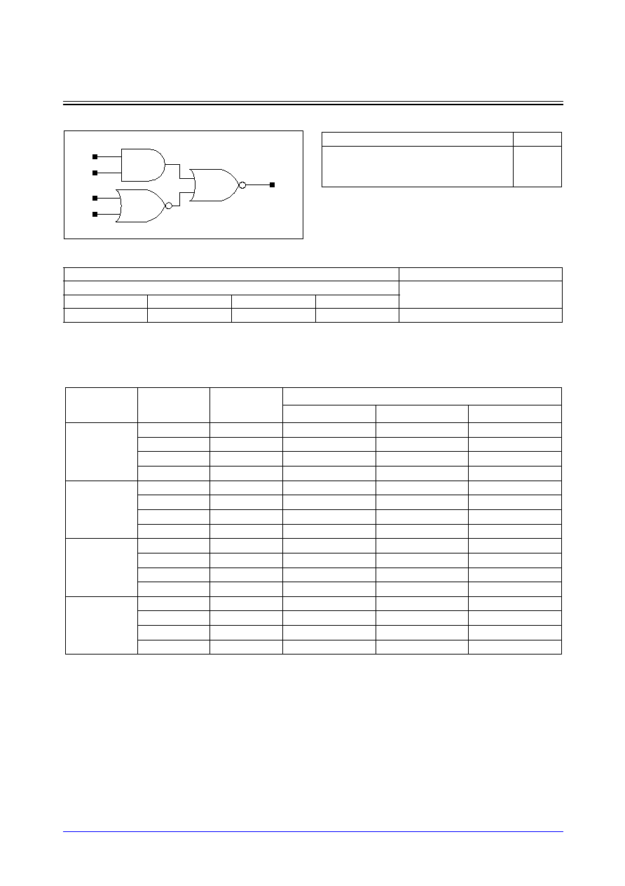
STDL131
3-96
Samsung ASIC
AO22A_LP
2-AND and 2-NOR into 2-NOR with 1X Drive
Logic Symbol
Cell Data
Switching Characteristics
(Typical process, 25
∞
C, 1.8V, t
R
/t
F
= 0.19ns, SL: Standard Load)
AO22A_LP
Input Load (SL)
Gate Count
AO22A_LP
AO22A_LP
A
B
C
D
1.1
1.1
0.9
0.9
3.00
Truth Table
A
B
C
D
Y
1
1
x
x
0
x
x
0
0
0
Other States
1
C
D
A
B
Y
Path
Parameter
Delay [ns]
SL = 2
Delay Equations [ns]
Group1*
Group2*
Group3*
A to Y
tR
0.242
0.140 + 0.051*SL
0.133 + 0.053*SL
0.125 + 0.054*SL
tF
0.150
0.095 + 0.027*SL
0.088 + 0.029*SL
0.079 + 0.030*SL
tPLH
0.159
0.107 + 0.026*SL
0.107 + 0.026*SL
0.108 + 0.026*SL
tPHL
0.110
0.075 + 0.017*SL
0.080 + 0.016*SL
0.080 + 0.016*SL
B to Y
tR
0.258
0.154 + 0.052*SL
0.148 + 0.053*SL
0.141 + 0.054*SL
tF
0.142
0.086 + 0.028*SL
0.079 + 0.030*SL
0.075 + 0.031*SL
tPLH
0.174
0.121 + 0.026*SL
0.122 + 0.026*SL
0.123 + 0.026*SL
tPHL
0.107
0.072 + 0.018*SL
0.076 + 0.016*SL
0.077 + 0.016*SL
C to Y
tR
0.239
0.132 + 0.053*SL
0.130 + 0.054*SL
0.129 + 0.054*SL
tF
0.177
0.115 + 0.031*SL
0.115 + 0.031*SL
0.115 + 0.031*SL
tPLH
0.248
0.195 + 0.027*SL
0.197 + 0.026*SL
0.198 + 0.026*SL
tPHL
0.227
0.191 + 0.018*SL
0.195 + 0.017*SL
0.198 + 0.017*SL
D to Y
tR
0.254
0.147 + 0.054*SL
0.146 + 0.054*SL
0.145 + 0.054*SL
tF
0.176
0.115 + 0.031*SL
0.114 + 0.031*SL
0.114 + 0.031*SL
tPLH
0.261
0.208 + 0.026*SL
0.209 + 0.026*SL
0.210 + 0.026*SL
tPHL
0.229
0.194 + 0.018*SL
0.197 + 0.017*SL
0.201 + 0.017*SL
*Group1 : SL < 4, *Group2 : 4 SL
<
<
=
= 8, *Group3 : 8 < SL
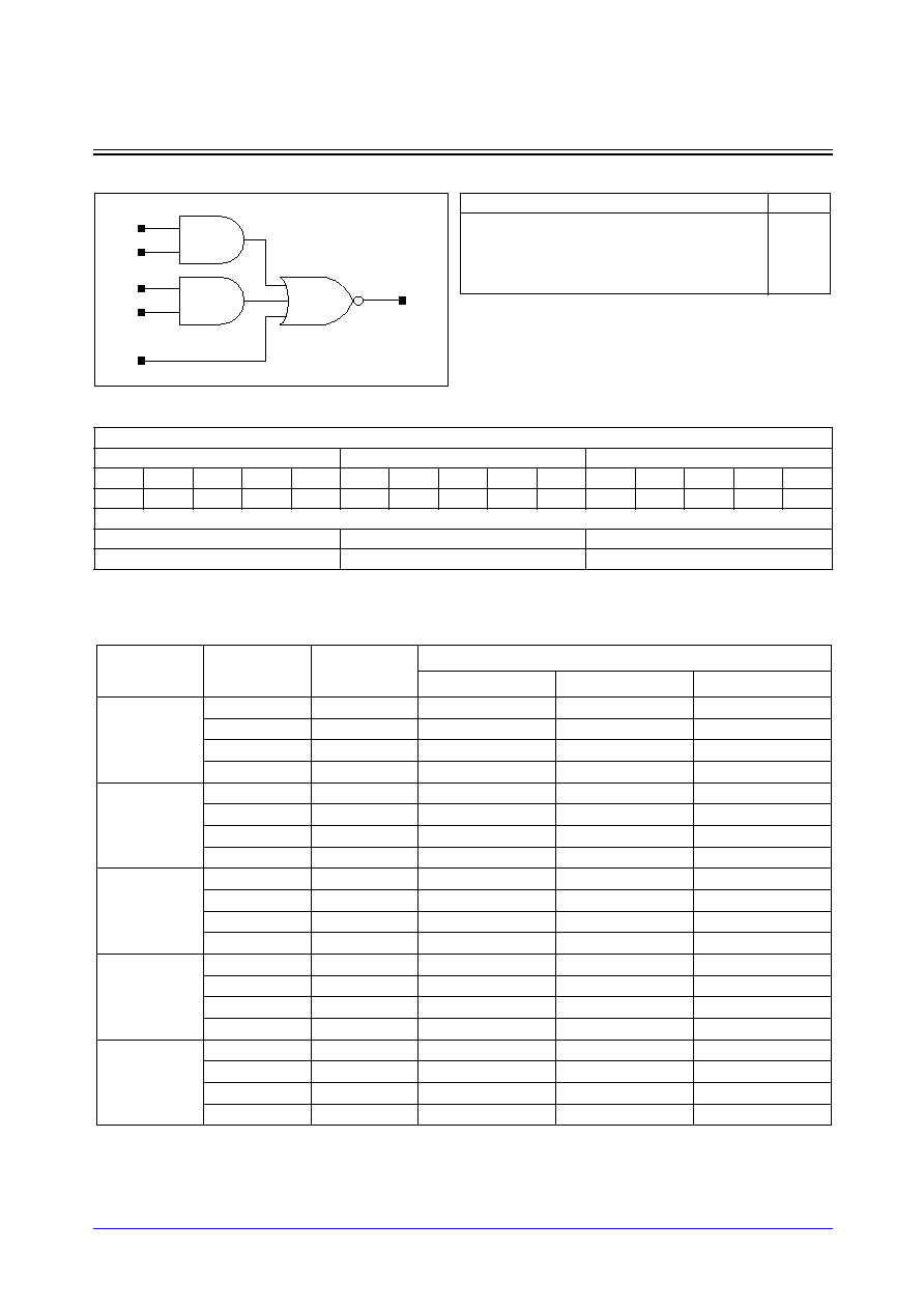
Samsung ASIC
3-97
STDL131
AO221_LP/AO221D2_LP/AO221D4_LP
Two 2-ANDs into 3-NOR with 1X/2X/4X Drive
Logic Symbol
Cell Data
Switching Characteristics
(Typical process, 25
∞
C, 1.8V, t
R
/t
F
= 0.19ns, SL: Standard Load)
AO221_LP
Input Load (SL)
AO221_LP
AO221D2_LP
AO221D4_LP
A
B
C
D
E
A
B
C
D
E
A
B
C
D
E
1.1
1.1
1.0
1.1
1.0
1.0
1.0
1.0
1.0
0.9
1.0
1.0
1.0
1.0
0.9
Gate Count
AO221_LP
AO221D2_LP
AO221D4_LP
2.33
3.33
3.67
C
D
A
B
Y
E
Path
Parameter
Delay [ns]
SL = 2
Delay Equations [ns]
Group1*
Group2*
Group3*
A to Y
tR
0.391
0.229 + 0.081*SL
0.223 + 0.083*SL
0.222 + 0.083*SL
tF
0.158
0.100 + 0.029*SL
0.093 + 0.031*SL
0.085 + 0.032*SL
tPLH
0.200
0.121 + 0.040*SL
0.118 + 0.040*SL
0.120 + 0.040*SL
tPHL
0.118
0.083 + 0.018*SL
0.085 + 0.017*SL
0.086 + 0.017*SL
B to Y
tR
0.413
0.250 + 0.081*SL
0.244 + 0.083*SL
0.245 + 0.083*SL
tF
0.152
0.092 + 0.030*SL
0.087 + 0.031*SL
0.081 + 0.032*SL
tPLH
0.219
0.139 + 0.040*SL
0.138 + 0.040*SL
0.140 + 0.040*SL
tPHL
0.114
0.078 + 0.018*SL
0.082 + 0.017*SL
0.083 + 0.017*SL
C to Y
tR
0.412
0.251 + 0.080*SL
0.247 + 0.081*SL
0.245 + 0.082*SL
tF
0.193
0.132 + 0.031*SL
0.128 + 0.032*SL
0.123 + 0.032*SL
tPLH
0.309
0.227 + 0.041*SL
0.229 + 0.040*SL
0.231 + 0.040*SL
tPHL
0.167
0.130 + 0.018*SL
0.133 + 0.018*SL
0.136 + 0.017*SL
D to Y
tR
0.432
0.271 + 0.081*SL
0.269 + 0.081*SL
0.266 + 0.082*SL
tF
0.190
0.127 + 0.032*SL
0.126 + 0.032*SL
0.123 + 0.032*SL
tPLH
0.329
0.248 + 0.041*SL
0.249 + 0.040*SL
0.250 + 0.040*SL
tPHL
0.164
0.127 + 0.018*SL
0.130 + 0.018*SL
0.134 + 0.017*SL
E to Y
tR
0.433
0.271 + 0.081*SL
0.269 + 0.081*SL
0.266 + 0.082*SL
tF
0.228
0.169 + 0.029*SL
0.168 + 0.030*SL
0.164 + 0.030*SL
tPLH
0.362
0.281 + 0.041*SL
0.283 + 0.040*SL
0.284 + 0.040*SL
tPHL
0.189
0.151 + 0.019*SL
0.156 + 0.018*SL
0.162 + 0.017*SL
*Group1 : SL < 4, *Group2 : 4 SL
<
<
=
= 8, *Group3 : 8 < SL
Truth Table
A
B
C
D
E
Y
1
1
x
x
x
0
x
x
1
1
x
0
x
x
x
x
1
0
Other States
1
STDL131
3-98
Samsung ASIC
AO221_LP/AO221D2_LP/AO221D4_LP
Two 2-ANDs into 3-NOR with 1X/2X/4X Drive
Switching Characteristics
(Typical process, 25
∞
C, 1.8V, t
R
/t
F
= 0.19ns, SL: Standard Load)
AO221D2_LP
Path
Parameter
Delay [ns]
SL = 2
Delay Equations [ns]
Group1*
Group2*
Group3*
A to Y
tR
0.067
0.045 + 0.011*SL
0.040 + 0.012*SL
0.033 + 0.013*SL
tF
0.066
0.047 + 0.010*SL
0.052 + 0.008*SL
0.049 + 0.008*SL
tPLH
0.281
0.266 + 0.008*SL
0.271 + 0.006*SL
0.273 + 0.006*SL
tPHL
0.295
0.279 + 0.008*SL
0.287 + 0.006*SL
0.299 + 0.005*SL
B to Y
tR
0.068
0.046 + 0.011*SL
0.040 + 0.012*SL
0.033 + 0.013*SL
tF
0.066
0.047 + 0.009*SL
0.052 + 0.008*SL
0.048 + 0.008*SL
tPLH
0.297
0.282 + 0.008*SL
0.286 + 0.006*SL
0.289 + 0.006*SL
tPHL
0.292
0.275 + 0.008*SL
0.284 + 0.006*SL
0.295 + 0.005*SL
C to Y
tR
0.067
0.043 + 0.012*SL
0.040 + 0.012*SL
0.033 + 0.013*SL
tF
0.066
0.047 + 0.009*SL
0.051 + 0.008*SL
0.050 + 0.008*SL
tPLH
0.371
0.356 + 0.008*SL
0.360 + 0.006*SL
0.363 + 0.006*SL
tPHL
0.358
0.342 + 0.008*SL
0.351 + 0.006*SL
0.362 + 0.005*SL
D to Y
tR
0.066
0.043 + 0.012*SL
0.040 + 0.013*SL
0.033 + 0.013*SL
tF
0.067
0.048 + 0.009*SL
0.053 + 0.008*SL
0.049 + 0.008*SL
tPLH
0.390
0.375 + 0.008*SL
0.380 + 0.006*SL
0.382 + 0.006*SL
tPHL
0.356
0.339 + 0.008*SL
0.348 + 0.006*SL
0.359 + 0.005*SL
E to Y
tR
0.066
0.042 + 0.012*SL
0.041 + 0.012*SL
0.033 + 0.013*SL
tF
0.067
0.047 + 0.010*SL
0.053 + 0.008*SL
0.052 + 0.008*SL
tPLH
0.425
0.410 + 0.008*SL
0.414 + 0.006*SL
0.417 + 0.006*SL
tPHL
0.413
0.396 + 0.008*SL
0.405 + 0.006*SL
0.417 + 0.005*SL
*Group1 : SL < 4, *Group2 : 4 SL
<
<
=
= 12, *Group3 : 12 < SL

Samsung ASIC
3-99
STDL131
AO221_LP/AO221D2_LP/AO221D4_LP
Two 2-ANDs into 3-NOR with 1X/2X/4X Drive
Switching Characteristics
(Typical process, 25
∞
C, 1.8V, t
R
/t
F
= 0.19ns, SL: Standard Load)
AO221D4_LP
Path
Parameter
Delay [ns]
SL = 2
Delay Equations [ns]
Group1*
Group2*
Group3*
A to Y
tR
0.067
0.056 + 0.006*SL
0.054 + 0.006*SL
0.043 + 0.006*SL
tF
0.070
0.058 + 0.006*SL
0.065 + 0.004*SL
0.068 + 0.004*SL
tPLH
0.315
0.305 + 0.005*SL
0.310 + 0.004*SL
0.318 + 0.003*SL
tPHL
0.328
0.317 + 0.006*SL
0.325 + 0.004*SL
0.344 + 0.003*SL
B to Y
tR
0.067
0.055 + 0.006*SL
0.056 + 0.006*SL
0.044 + 0.006*SL
tF
0.070
0.059 + 0.006*SL
0.065 + 0.004*SL
0.069 + 0.004*SL
tPLH
0.330
0.320 + 0.005*SL
0.326 + 0.004*SL
0.334 + 0.003*SL
tPHL
0.324
0.313 + 0.006*SL
0.321 + 0.004*SL
0.340 + 0.003*SL
C to Y
tR
0.067
0.055 + 0.006*SL
0.055 + 0.006*SL
0.045 + 0.006*SL
tF
0.070
0.058 + 0.006*SL
0.065 + 0.004*SL
0.069 + 0.004*SL
tPLH
0.404
0.394 + 0.005*SL
0.400 + 0.004*SL
0.408 + 0.003*SL
tPHL
0.391
0.380 + 0.006*SL
0.387 + 0.004*SL
0.407 + 0.003*SL
D to Y
tR
0.067
0.055 + 0.006*SL
0.054 + 0.006*SL
0.045 + 0.006*SL
tF
0.071
0.059 + 0.006*SL
0.065 + 0.004*SL
0.069 + 0.004*SL
tPLH
0.422
0.412 + 0.005*SL
0.418 + 0.004*SL
0.426 + 0.003*SL
tPHL
0.388
0.377 + 0.006*SL
0.385 + 0.004*SL
0.404 + 0.003*SL
E to Y
tR
0.067
0.056 + 0.006*SL
0.055 + 0.006*SL
0.045 + 0.006*SL
tF
0.072
0.061 + 0.006*SL
0.066 + 0.004*SL
0.070 + 0.004*SL
tPLH
0.457
0.447 + 0.005*SL
0.453 + 0.004*SL
0.461 + 0.003*SL
tPHL
0.446
0.435 + 0.006*SL
0.443 + 0.004*SL
0.462 + 0.003*SL
*Group1 : SL < 4, *Group2 : 4 SL
<
<
=
= 20, *Group3 : 20 < SL
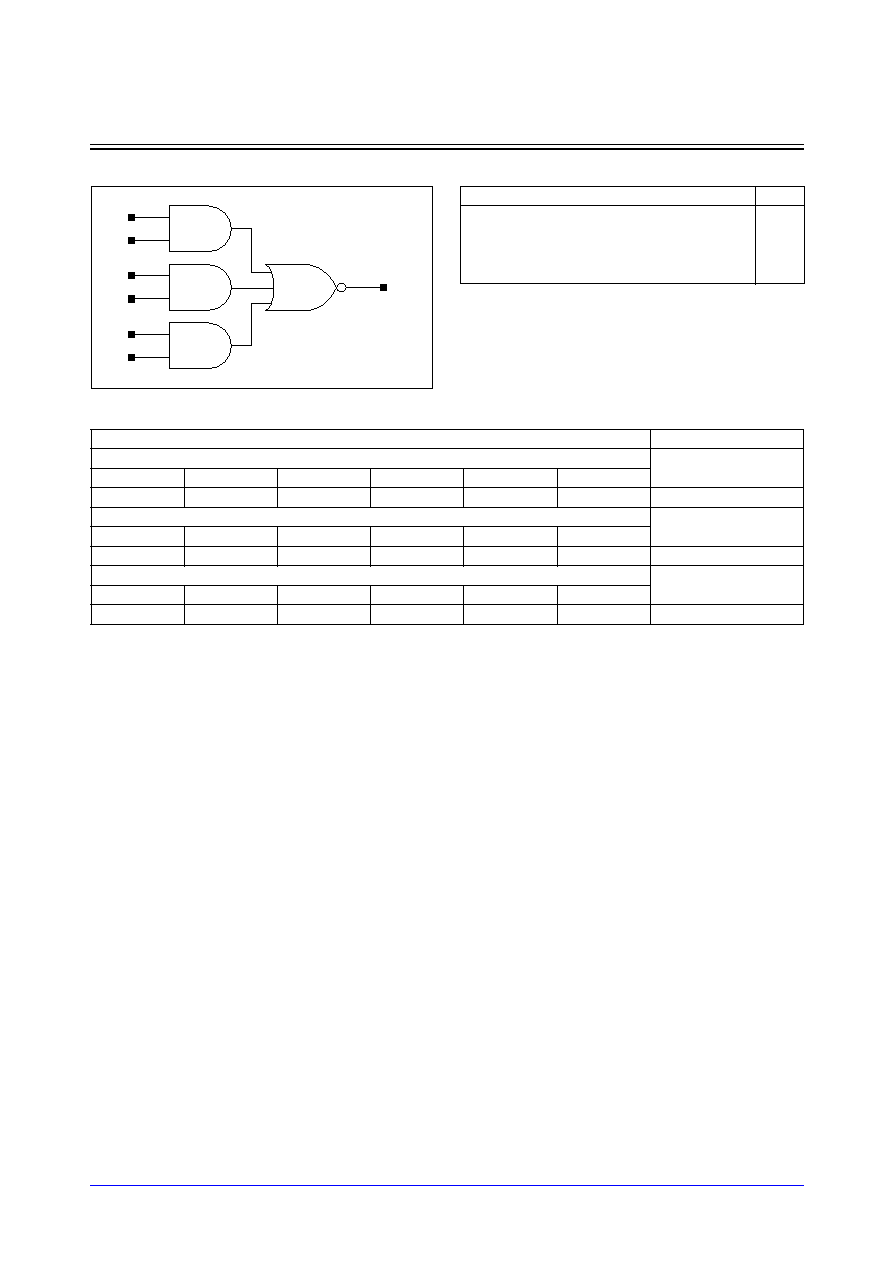
STDL131
3-100
Samsung ASIC
AO222_LP/AO222D2_LP/AO222D4_LP
Three 2-ANDs into 3-NOR with 1X/2X/4X Drive
Logic Symbol
Cell Data
Input Load (SL)
Gate Count
AO222_LP
AO222_LP
A
B
C
D
E
F
1.0
1.0
1.0
1.1
1.1
1.1
2.67
AO222D2_LP
AO222D2_LP
A
B
C
D
E
F
0.9
0.9
0.9
0.9
0.9
0.9
3.67
AO222D4_LP
AO222D4_LP
A
B
C
D
E
F
0.9
0.9
0.9
0.9
0.9
0.9
4.33
C
D
A
B
Y
E
F
Truth Table
A
B
C
D
E
F
Y
1
1
x
x
x
x
0
x
x
1
1
x
x
0
x
x
x
x
1
1
0
Other States
1

Samsung ASIC
3-101
STDL131
AO222_LP/AO222D2_LP/AO222D4_LP
Three 2-ANDs into 3-NOR with 1X/2X/4X Drive
Switching Characteristics
(Typical process, 25
∞
C, 1.8V, t
R
/t
F
= 0.19ns, SL: Standard Load)
AO222_LP
Path
Parameter
Delay [ns]
SL = 2
Delay Equations [ns]
Group1*
Group2*
Group3*
A to Y
tR
0.421
0.257 + 0.082*SL
0.251 + 0.084*SL
0.253 + 0.083*SL
tF
0.178
0.118 + 0.030*SL
0.111 + 0.032*SL
0.103 + 0.033*SL
tPLH
0.224
0.143 + 0.041*SL
0.143 + 0.041*SL
0.145 + 0.040*SL
tPHL
0.123
0.086 + 0.018*SL
0.088 + 0.018*SL
0.089 + 0.018*SL
B to Y
tR
0.441
0.276 + 0.082*SL
0.272 + 0.084*SL
0.275 + 0.083*SL
tF
0.173
0.110 + 0.031*SL
0.106 + 0.032*SL
0.100 + 0.033*SL
tPLH
0.242
0.161 + 0.041*SL
0.162 + 0.040*SL
0.164 + 0.040*SL
tPHL
0.119
0.082 + 0.018*SL
0.085 + 0.018*SL
0.086 + 0.018*SL
C to Y
tR
0.440
0.278 + 0.081*SL
0.276 + 0.082*SL
0.273 + 0.082*SL
tF
0.215
0.151 + 0.032*SL
0.148 + 0.033*SL
0.143 + 0.033*SL
tPLH
0.331
0.249 + 0.041*SL
0.251 + 0.040*SL
0.253 + 0.040*SL
tPHL
0.173
0.135 + 0.019*SL
0.138 + 0.018*SL
0.141 + 0.018*SL
D to Y
tR
0.462
0.300 + 0.081*SL
0.297 + 0.082*SL
0.295 + 0.082*SL
tF
0.212
0.148 + 0.032*SL
0.144 + 0.033*SL
0.143 + 0.033*SL
tPLH
0.352
0.270 + 0.041*SL
0.272 + 0.040*SL
0.273 + 0.040*SL
tPHL
0.170
0.132 + 0.019*SL
0.135 + 0.018*SL
0.138 + 0.018*SL
E to Y
tR
0.440
0.278 + 0.081*SL
0.276 + 0.082*SL
0.273 + 0.082*SL
tF
0.249
0.183 + 0.033*SL
0.182 + 0.033*SL
0.180 + 0.034*SL
tPLH
0.374
0.292 + 0.041*SL
0.294 + 0.040*SL
0.296 + 0.040*SL
tPHL
0.200
0.159 + 0.021*SL
0.164 + 0.019*SL
0.171 + 0.018*SL
F to Y
tR
0.462
0.300 + 0.081*SL
0.297 + 0.082*SL
0.295 + 0.082*SL
tF
0.249
0.182 + 0.033*SL
0.182 + 0.033*SL
0.182 + 0.033*SL
tPLH
0.394
0.313 + 0.041*SL
0.314 + 0.040*SL
0.316 + 0.040*SL
tPHL
0.197
0.156 + 0.021*SL
0.162 + 0.019*SL
0.168 + 0.018*SL
*Group1 : SL < 4, *Group2 : 4 SL
<
<
=
= 8, *Group3 : 8 < SL

STDL131
3-102
Samsung ASIC
AO222_LP/AO222D2_LP/AO222D4_LP
Three 2-ANDs into 3-NOR with 1X/2X/4X Drive
Switching Characteristics
(Typical process, 25
∞
C, 1.8V, t
R
/t
F
= 0.19ns, SL: Standard Load)
AO222D2_LP
Path
Parameter
Delay [ns]
SL = 2
Delay Equations [ns]
Group1*
Group2*
Group3*
A to Y
tR
0.067
0.043 + 0.012*SL
0.041 + 0.013*SL
0.033 + 0.013*SL
tF
0.059
0.041 + 0.009*SL
0.045 + 0.008*SL
0.038 + 0.008*SL
tPLH
0.293
0.278 + 0.008*SL
0.283 + 0.006*SL
0.285 + 0.006*SL
tPHL
0.301
0.286 + 0.008*SL
0.294 + 0.006*SL
0.302 + 0.005*SL
B to Y
tR
0.068
0.045 + 0.011*SL
0.041 + 0.013*SL
0.033 + 0.013*SL
tF
0.058
0.040 + 0.009*SL
0.044 + 0.008*SL
0.040 + 0.008*SL
tPLH
0.305
0.290 + 0.008*SL
0.295 + 0.006*SL
0.297 + 0.006*SL
tPHL
0.298
0.283 + 0.007*SL
0.290 + 0.006*SL
0.299 + 0.005*SL
C to Y
tR
0.069
0.046 + 0.011*SL
0.041 + 0.013*SL
0.033 + 0.013*SL
tF
0.059
0.042 + 0.009*SL
0.045 + 0.008*SL
0.040 + 0.008*SL
tPLH
0.401
0.386 + 0.008*SL
0.390 + 0.007*SL
0.393 + 0.006*SL
tPHL
0.395
0.380 + 0.008*SL
0.387 + 0.006*SL
0.396 + 0.005*SL
D to Y
tR
0.069
0.046 + 0.011*SL
0.041 + 0.013*SL
0.033 + 0.013*SL
tF
0.059
0.042 + 0.008*SL
0.044 + 0.008*SL
0.040 + 0.008*SL
tPLH
0.414
0.399 + 0.008*SL
0.403 + 0.007*SL
0.406 + 0.006*SL
tPHL
0.392
0.377 + 0.008*SL
0.384 + 0.006*SL
0.393 + 0.005*SL
E to Y
tR
0.069
0.046 + 0.011*SL
0.041 + 0.013*SL
0.033 + 0.013*SL
tF
0.061
0.043 + 0.009*SL
0.047 + 0.008*SL
0.042 + 0.008*SL
tPLH
0.444
0.429 + 0.008*SL
0.433 + 0.007*SL
0.436 + 0.006*SL
tPHL
0.457
0.442 + 0.008*SL
0.449 + 0.006*SL
0.458 + 0.005*SL
F to Y
tR
0.068
0.044 + 0.012*SL
0.041 + 0.013*SL
0.033 + 0.013*SL
tF
0.061
0.044 + 0.009*SL
0.046 + 0.008*SL
0.041 + 0.008*SL
tPLH
0.457
0.442 + 0.008*SL
0.446 + 0.007*SL
0.449 + 0.006*SL
tPHL
0.454
0.439 + 0.008*SL
0.446 + 0.006*SL
0.455 + 0.005*SL
*Group1 : SL < 4, *Group2 : 4 SL
<
<
=
= 12, *Group3 : 12 < SL

Samsung ASIC
3-103
STDL131
AO222_LP/AO222D2_LP/AO222D4_LP
Three 2-ANDs into 3-NOR with 1X/2X/4X Drive
Switching Characteristics
(Typical process, 25
∞
C, 1.8V, t
R
/t
F
= 0.19ns, SL: Standard Load)
AO222D4_LP
Path
Parameter
Delay [ns]
SL = 2
Delay Equations [ns]
Group1*
Group2*
Group3*
A to Y
tR
0.068
0.055 + 0.006*SL
0.056 + 0.006*SL
0.046 + 0.006*SL
tF
0.063
0.053 + 0.005*SL
0.056 + 0.004*SL
0.058 + 0.004*SL
tPLH
0.327
0.317 + 0.005*SL
0.323 + 0.004*SL
0.332 + 0.003*SL
tPHL
0.338
0.328 + 0.005*SL
0.335 + 0.003*SL
0.351 + 0.003*SL
B to Y
tR
0.067
0.056 + 0.005*SL
0.054 + 0.006*SL
0.045 + 0.006*SL
tF
0.063
0.054 + 0.005*SL
0.055 + 0.004*SL
0.057 + 0.004*SL
tPLH
0.340
0.330 + 0.005*SL
0.335 + 0.004*SL
0.344 + 0.003*SL
tPHL
0.335
0.324 + 0.005*SL
0.331 + 0.003*SL
0.348 + 0.003*SL
C to Y
tR
0.069
0.056 + 0.006*SL
0.057 + 0.006*SL
0.046 + 0.006*SL
tF
0.064
0.054 + 0.005*SL
0.058 + 0.004*SL
0.058 + 0.004*SL
tPLH
0.435
0.425 + 0.005*SL
0.431 + 0.004*SL
0.439 + 0.003*SL
tPHL
0.432
0.421 + 0.005*SL
0.429 + 0.003*SL
0.445 + 0.003*SL
D to Y
tR
0.069
0.057 + 0.006*SL
0.057 + 0.006*SL
0.046 + 0.006*SL
tF
0.064
0.053 + 0.005*SL
0.058 + 0.004*SL
0.058 + 0.004*SL
tPLH
0.448
0.438 + 0.005*SL
0.444 + 0.004*SL
0.453 + 0.003*SL
tPHL
0.429
0.419 + 0.005*SL
0.426 + 0.003*SL
0.442 + 0.003*SL
E to Y
tR
0.068
0.056 + 0.006*SL
0.056 + 0.006*SL
0.046 + 0.006*SL
tF
0.065
0.055 + 0.005*SL
0.059 + 0.004*SL
0.060 + 0.004*SL
tPLH
0.478
0.468 + 0.005*SL
0.474 + 0.004*SL
0.482 + 0.003*SL
tPHL
0.495
0.485 + 0.005*SL
0.492 + 0.003*SL
0.508 + 0.003*SL
F to Y
tR
0.069
0.057 + 0.006*SL
0.057 + 0.006*SL
0.046 + 0.006*SL
tF
0.066
0.055 + 0.005*SL
0.060 + 0.004*SL
0.060 + 0.004*SL
tPLH
0.491
0.481 + 0.005*SL
0.487 + 0.004*SL
0.495 + 0.003*SL
tPHL
0.492
0.482 + 0.005*SL
0.489 + 0.003*SL
0.506 + 0.003*SL
*Group1 : SL < 4, *Group2 : 4 SL
<
<
=
= 20, *Group3 : 20 < SL
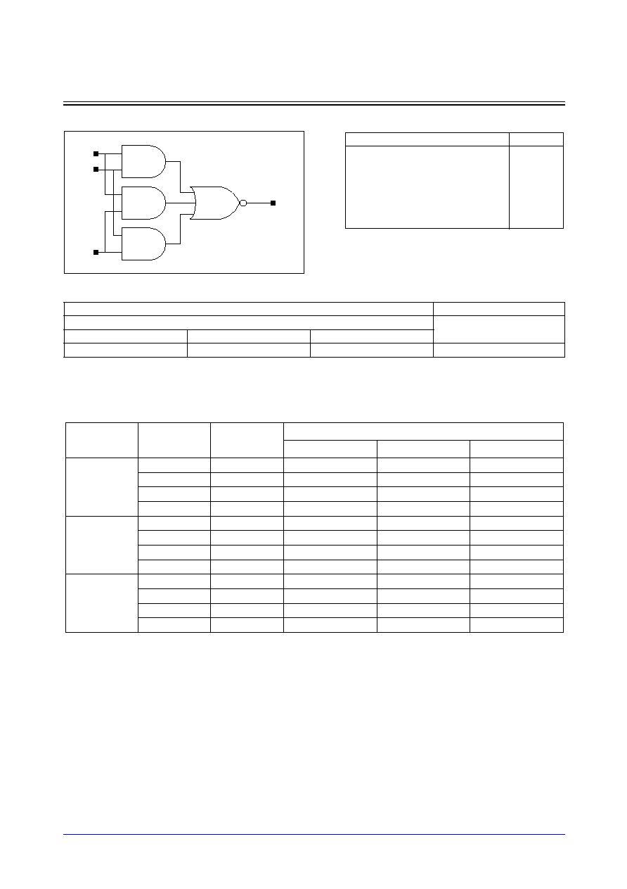
STDL131
3-104
Samsung ASIC
AO222A_LP
Inverting 2-of-3 Majority with 1X Drive
Logic Symbol
Cell Data
Switching Characteristics
(Typical process, 25
∞
C, 1.8V, t
R
/t
F
= 0.19ns, SL: Standard Load)
AO222A_LP
Input Load (SL)
Gate Count
AO222A_LP
AO222A_LP
A
B
C
2.0
2.2
2.2
2.33
Truth Table
A
B
C
Y
1
1
x
0
1
x
1
0
x
1
1
0
0
0
x
1
0
x
0
1
x
0
0
1
A
B
Y
C
Path
Parameter
Delay [ns]
SL = 2
Delay Equations [ns]
Group1*
Group2*
Group3*
A to Y
tR
0.398
0.294 + 0.052*SL
0.285 + 0.054*SL
0.280 + 0.055*SL
tF
0.169
0.118 + 0.025*SL
0.115 + 0.026*SL
0.109 + 0.027*SL
tPLH
0.205
0.151 + 0.027*SL
0.151 + 0.027*SL
0.153 + 0.027*SL
tPHL
0.146
0.116 + 0.015*SL
0.118 + 0.015*SL
0.120 + 0.014*SL
B to Y
tR
0.395
0.288 + 0.053*SL
0.282 + 0.055*SL
0.281 + 0.055*SL
tF
0.177
0.125 + 0.026*SL
0.124 + 0.026*SL
0.119 + 0.027*SL
tPLH
0.217
0.163 + 0.027*SL
0.164 + 0.027*SL
0.166 + 0.026*SL
tPHL
0.163
0.132 + 0.015*SL
0.134 + 0.015*SL
0.137 + 0.014*SL
C to Y
tR
0.361
0.254 + 0.053*SL
0.251 + 0.054*SL
0.248 + 0.055*SL
tF
0.179
0.127 + 0.026*SL
0.126 + 0.026*SL
0.121 + 0.027*SL
tPLH
0.230
0.177 + 0.026*SL
0.178 + 0.026*SL
0.179 + 0.026*SL
tPHL
0.148
0.118 + 0.015*SL
0.120 + 0.015*SL
0.122 + 0.014*SL
*Group1 : SL < 4, *Group2 : 4 SL
<
<
=
= 8, *Group3 : 8 < SL
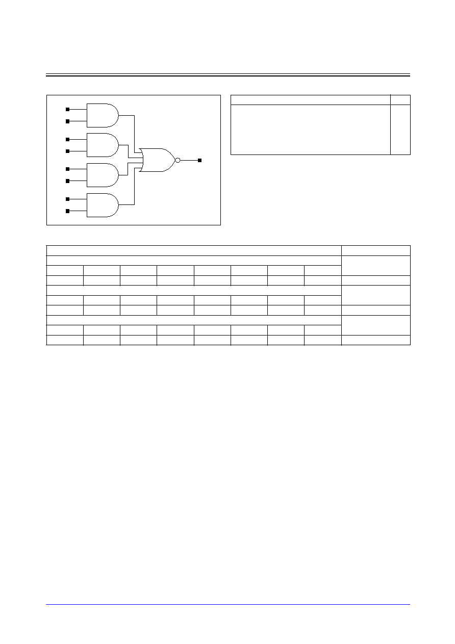
Samsung ASIC
3-105
STDL131
AO2222_LP/AO2222D2_LP/AO2222D4_LP
Four 2-ANDs into 4-NOR with 1X/2X/4X Drive
Logic Symbol
Cell Data
Input Load (SL)
Gate Count
AO2222_LP
AO2222_LP
A
B
C
D
E
F
G
H
1.0
1.0
1.0
1.0
1.0
1.0
1.0
1.0
3.33
AO2222D2_LP
AO2222D2_LP
A
B
C
D
E
F
G
H
0.9
0.9
0.9
0.9
0.9
0.9
1.0
1.0
4.33
AO2222D4_LP
AO2222D4_LP
A
B
C
D
E
F
G
H
0.9
0.9
0.9
0.9
0.9
0.9
1.0
1.0
5.00
Y
C
D
A
B
E
F
G
H
Truth Table
A
B
C
D
E
F
G
H
Y
1
1
x
x
x
x
x
x
0
x
x
1
1
x
x
x
x
0
x
x
x
x
1
1
x
x
0
x
x
x
x
x
x
1
1
0
Other States
1

STDL131
3-106
Samsung ASIC
AO2222_LP/AO2222D2_LP/AO2222D4_LP
Four 2-ANDs into 4-NOR with 1X/2X/4X Drive
Switching Characteristics
(Typical process, 25
∞
C, 1.8V, t
R
/t
F
= 0.19ns, SL: Standard Load)
AO2222_LP
Path
Parameter
Delay [ns]
SL = 2
Delay Equations [ns]
Group1*
Group2*
Group3*
A to Y
tR
0.570
0.346 + 0.112*SL
0.341 + 0.113*SL
0.348 + 0.113*SL
tF
0.236
0.149 + 0.043*SL
0.142 + 0.045*SL
0.134 + 0.046*SL
tPLH
0.237
0.133 + 0.052*SL
0.123 + 0.054*SL
0.125 + 0.054*SL
tPHL
0.155
0.105 + 0.025*SL
0.107 + 0.025*SL
0.108 + 0.024*SL
B to Y
tR
0.592
0.367 + 0.112*SL
0.362 + 0.113*SL
0.370 + 0.113*SL
tF
0.233
0.144 + 0.044*SL
0.139 + 0.046*SL
0.135 + 0.046*SL
tPLH
0.253
0.148 + 0.053*SL
0.142 + 0.054*SL
0.143 + 0.054*SL
tPHL
0.152
0.102 + 0.025*SL
0.104 + 0.025*SL
0.105 + 0.024*SL
C to Y
tR
0.634
0.416 + 0.109*SL
0.413 + 0.109*SL
0.411 + 0.110*SL
tF
0.298
0.208 + 0.045*SL
0.205 + 0.046*SL
0.202 + 0.046*SL
tPLH
0.399
0.289 + 0.055*SL
0.291 + 0.054*SL
0.294 + 0.054*SL
tPHL
0.230
0.178 + 0.026*SL
0.181 + 0.025*SL
0.184 + 0.025*SL
D to Y
tR
0.653
0.436 + 0.109*SL
0.433 + 0.109*SL
0.431 + 0.110*SL
tF
0.297
0.206 + 0.046*SL
0.205 + 0.046*SL
0.203 + 0.046*SL
tPLH
0.418
0.308 + 0.055*SL
0.310 + 0.054*SL
0.312 + 0.054*SL
tPHL
0.227
0.175 + 0.026*SL
0.179 + 0.025*SL
0.182 + 0.025*SL
E to Y
tR
0.657
0.441 + 0.108*SL
0.437 + 0.109*SL
0.433 + 0.109*SL
tF
0.356
0.264 + 0.046*SL
0.262 + 0.046*SL
0.264 + 0.046*SL
tPLH
0.509
0.399 + 0.055*SL
0.401 + 0.054*SL
0.404 + 0.054*SL
tPHL
0.266
0.211 + 0.027*SL
0.217 + 0.026*SL
0.223 + 0.025*SL
F to Y
tR
0.669
0.455 + 0.107*SL
0.452 + 0.108*SL
0.448 + 0.108*SL
tF
0.357
0.264 + 0.046*SL
0.264 + 0.046*SL
0.264 + 0.046*SL
tPLH
0.523
0.415 + 0.054*SL
0.417 + 0.054*SL
0.419 + 0.054*SL
tPHL
0.263
0.208 + 0.027*SL
0.214 + 0.026*SL
0.220 + 0.025*SL
G to Y
tR
0.656
0.440 + 0.108*SL
0.436 + 0.109*SL
0.432 + 0.109*SL
tF
0.418
0.322 + 0.048*SL
0.323 + 0.048*SL
0.327 + 0.047*SL
tPLH
0.558
0.448 + 0.055*SL
0.451 + 0.054*SL
0.453 + 0.054*SL
tPHL
0.289
0.229 + 0.030*SL
0.237 + 0.028*SL
0.248 + 0.026*SL
H to Y
tR
0.669
0.455 + 0.107*SL
0.452 + 0.108*SL
0.448 + 0.108*SL
tF
0.418
0.322 + 0.048*SL
0.324 + 0.048*SL
0.329 + 0.047*SL
tPLH
0.573
0.465 + 0.054*SL
0.467 + 0.054*SL
0.469 + 0.053*SL
tPHL
0.286
0.227 + 0.030*SL
0.235 + 0.028*SL
0.246 + 0.026*SL
*Group1 : SL < 4, *Group2 : 4 SL
<
<
=
= 8, *Group3 : 8 < SL

Samsung ASIC
3-107
STDL131
AO2222_LP/AO2222D2_LP/AO2222D4_LP
Four 2-ANDs into 4-NOR with 1X/2X/4X Drive
Switching Characteristics
(Typical process, 25
∞
C, 1.8V, t
R
/t
F
= 0.19ns, SL: Standard Load)
AO2222D2_LP
Path
Parameter
Delay [ns]
SL = 2
Delay Equations [ns]
Group1*
Group2*
Group3*
A to Y
tR
0.068
0.045 + 0.012*SL
0.042 + 0.013*SL
0.034 + 0.013*SL
tF
0.066
0.048 + 0.009*SL
0.053 + 0.008*SL
0.048 + 0.008*SL
tPLH
0.295
0.279 + 0.008*SL
0.284 + 0.007*SL
0.287 + 0.006*SL
tPHL
0.335
0.318 + 0.008*SL
0.327 + 0.006*SL
0.338 + 0.005*SL
B to Y
tR
0.070
0.048 + 0.011*SL
0.043 + 0.012*SL
0.034 + 0.013*SL
tF
0.066
0.048 + 0.009*SL
0.051 + 0.008*SL
0.050 + 0.008*SL
tPLH
0.309
0.294 + 0.008*SL
0.299 + 0.006*SL
0.301 + 0.006*SL
tPHL
0.331
0.315 + 0.008*SL
0.324 + 0.006*SL
0.335 + 0.005*SL
C to Y
tR
0.072
0.050 + 0.011*SL
0.044 + 0.012*SL
0.035 + 0.013*SL
tF
0.067
0.049 + 0.009*SL
0.054 + 0.008*SL
0.049 + 0.008*SL
tPLH
0.453
0.438 + 0.008*SL
0.443 + 0.007*SL
0.446 + 0.006*SL
tPHL
0.435
0.419 + 0.008*SL
0.427 + 0.006*SL
0.439 + 0.005*SL
D to Y
tR
0.072
0.050 + 0.011*SL
0.044 + 0.012*SL
0.036 + 0.013*SL
tF
0.067
0.049 + 0.009*SL
0.054 + 0.008*SL
0.049 + 0.008*SL
tPLH
0.470
0.454 + 0.008*SL
0.460 + 0.006*SL
0.462 + 0.006*SL
tPHL
0.432
0.416 + 0.008*SL
0.424 + 0.006*SL
0.436 + 0.005*SL
E to Y
tR
0.072
0.049 + 0.011*SL
0.044 + 0.012*SL
0.035 + 0.013*SL
tF
0.069
0.051 + 0.009*SL
0.053 + 0.008*SL
0.052 + 0.008*SL
tPLH
0.560
0.545 + 0.008*SL
0.550 + 0.007*SL
0.553 + 0.006*SL
tPHL
0.495
0.478 + 0.008*SL
0.487 + 0.006*SL
0.499 + 0.005*SL
F to Y
tR
0.072
0.050 + 0.011*SL
0.045 + 0.012*SL
0.035 + 0.013*SL
tF
0.069
0.051 + 0.009*SL
0.055 + 0.008*SL
0.051 + 0.008*SL
tPLH
0.576
0.560 + 0.008*SL
0.565 + 0.007*SL
0.568 + 0.006*SL
tPHL
0.492
0.475 + 0.008*SL
0.484 + 0.006*SL
0.496 + 0.005*SL
G to Y
tR
0.071
0.049 + 0.011*SL
0.044 + 0.012*SL
0.035 + 0.013*SL
tF
0.070
0.052 + 0.009*SL
0.057 + 0.008*SL
0.054 + 0.008*SL
tPLH
0.603
0.588 + 0.008*SL
0.593 + 0.007*SL
0.596 + 0.006*SL
tPHL
0.535
0.518 + 0.008*SL
0.527 + 0.006*SL
0.539 + 0.005*SL
H to Y
tR
0.072
0.050 + 0.011*SL
0.044 + 0.012*SL
0.035 + 0.013*SL
tF
0.071
0.053 + 0.009*SL
0.056 + 0.008*SL
0.055 + 0.008*SL
tPLH
0.618
0.602 + 0.008*SL
0.607 + 0.007*SL
0.610 + 0.006*SL
tPHL
0.533
0.516 + 0.008*SL
0.525 + 0.006*SL
0.537 + 0.005*SL
*Group1 : SL < 4, *Group2 : 4 SL
<
<
=
= 12, *Group3 : 12 < SL
STDL131
3-108
Samsung ASIC
AO2222_LP/AO2222D2_LP/AO2222D4_LP
Four 2-ANDs into 4-NOR with 1X/2X/4X Drive
Switching Characteristics
(Typical process, 25
∞
C, 1.8V, t
R
/t
F
= 0.19ns, SL: Standard Load)
AO2222D4_LP
Path
Parameter
Delay [ns]
SL = 2
Delay Equations [ns]
Group1*
Group2*
Group3*
A to Y
tR
0.071
0.058 + 0.006*SL
0.060 + 0.006*SL
0.048 + 0.006*SL
tF
0.078
0.066 + 0.006*SL
0.072 + 0.004*SL
0.078 + 0.004*SL
tPLH
0.333
0.322 + 0.005*SL
0.329 + 0.004*SL
0.338 + 0.003*SL
tPHL
0.392
0.380 + 0.006*SL
0.389 + 0.004*SL
0.410 + 0.003*SL
B to Y
tR
0.072
0.060 + 0.006*SL
0.060 + 0.006*SL
0.049 + 0.006*SL
tF
0.077
0.065 + 0.006*SL
0.071 + 0.004*SL
0.078 + 0.004*SL
tPLH
0.348
0.337 + 0.005*SL
0.344 + 0.004*SL
0.353 + 0.003*SL
tPHL
0.389
0.377 + 0.006*SL
0.385 + 0.004*SL
0.407 + 0.003*SL
C to Y
tR
0.071
0.058 + 0.007*SL
0.062 + 0.006*SL
0.050 + 0.006*SL
tF
0.078
0.066 + 0.006*SL
0.072 + 0.004*SL
0.078 + 0.004*SL
tPLH
0.492
0.482 + 0.005*SL
0.488 + 0.004*SL
0.498 + 0.003*SL
tPHL
0.492
0.480 + 0.006*SL
0.489 + 0.004*SL
0.511 + 0.003*SL
D to Y
tR
0.072
0.060 + 0.006*SL
0.061 + 0.006*SL
0.050 + 0.006*SL
tF
0.078
0.066 + 0.006*SL
0.073 + 0.004*SL
0.078 + 0.004*SL
tPLH
0.509
0.499 + 0.005*SL
0.505 + 0.004*SL
0.515 + 0.003*SL
tPHL
0.490
0.477 + 0.006*SL
0.486 + 0.004*SL
0.508 + 0.003*SL
E to Y
tR
0.073
0.061 + 0.006*SL
0.063 + 0.006*SL
0.050 + 0.006*SL
tF
0.079
0.067 + 0.006*SL
0.074 + 0.004*SL
0.079 + 0.004*SL
tPLH
0.600
0.590 + 0.005*SL
0.596 + 0.004*SL
0.606 + 0.003*SL
tPHL
0.554
0.542 + 0.006*SL
0.551 + 0.004*SL
0.573 + 0.003*SL
F to Y
tR
0.073
0.061 + 0.006*SL
0.063 + 0.006*SL
0.051 + 0.006*SL
tF
0.080
0.068 + 0.006*SL
0.075 + 0.004*SL
0.080 + 0.004*SL
tPLH
0.616
0.606 + 0.005*SL
0.612 + 0.004*SL
0.622 + 0.003*SL
tPHL
0.552
0.539 + 0.006*SL
0.548 + 0.004*SL
0.570 + 0.003*SL
G to Y
tR
0.073
0.062 + 0.006*SL
0.062 + 0.006*SL
0.049 + 0.006*SL
tF
0.082
0.071 + 0.006*SL
0.076 + 0.004*SL
0.083 + 0.004*SL
tPLH
0.643
0.632 + 0.005*SL
0.639 + 0.004*SL
0.648 + 0.003*SL
tPHL
0.597
0.585 + 0.006*SL
0.594 + 0.004*SL
0.617 + 0.003*SL
H to Y
tR
0.073
0.061 + 0.006*SL
0.063 + 0.006*SL
0.051 + 0.006*SL
tF
0.082
0.070 + 0.006*SL
0.076 + 0.004*SL
0.082 + 0.004*SL
tPLH
0.658
0.648 + 0.005*SL
0.654 + 0.004*SL
0.664 + 0.003*SL
tPHL
0.595
0.583 + 0.006*SL
0.592 + 0.004*SL
0.614 + 0.003*SL
*Group1 : SL < 4, *Group2 : 4 SL
<
<
=
= 20, *Group3 : 20 < SL
Samsung ASIC
3-109
STDL131
AO31_LP/AO31D2_LP/AO31D4_LP
3-AND into 2-NOR with 1X/2X/4X Drive
Logic Symbol
Cell Data
Switching Characteristics
(Typical process, 25
∞
C, 1.8V, t
R
/t
F
= 0.19ns, SL: Standard Load)
AO31_LP
Input Load (SL)
AO31_LP
AO31D2_LP
AO31D4_LP
A
B
C
D
A
B
C
D
A
B
C
D
1.1
1.1
1.1
1.1
2.2
2.3
2.2
2.1
0.9
0.9
0.9
0.8
Gate Count
AO31_LP
AO31D2_LP
AO31D4_LP
1.67
3.00
3.33
Y
D
A
B
C
Path
Parameter
Delay [ns]
SL = 2
Delay Equations [ns]
Group1*
Group2*
Group3*
A to Y
tR
0.258
0.154 + 0.052*SL
0.147 + 0.054*SL
0.139 + 0.055*SL
tF
0.178
0.108 + 0.035*SL
0.101 + 0.037*SL
0.094 + 0.038*SL
tPLH
0.162
0.109 + 0.027*SL
0.109 + 0.027*SL
0.110 + 0.026*SL
tPHL
0.132
0.093 + 0.020*SL
0.093 + 0.020*SL
0.094 + 0.020*SL
B to Y
tR
0.274
0.170 + 0.052*SL
0.163 + 0.054*SL
0.156 + 0.055*SL
tF
0.175
0.103 + 0.036*SL
0.098 + 0.037*SL
0.093 + 0.038*SL
tPLH
0.178
0.125 + 0.027*SL
0.125 + 0.027*SL
0.126 + 0.026*SL
tPHL
0.135
0.095 + 0.020*SL
0.096 + 0.020*SL
0.098 + 0.020*SL
C to Y
tR
0.291
0.186 + 0.052*SL
0.180 + 0.054*SL
0.174 + 0.055*SL
tF
0.171
0.098 + 0.036*SL
0.094 + 0.037*SL
0.092 + 0.038*SL
tPLH
0.192
0.138 + 0.027*SL
0.139 + 0.027*SL
0.141 + 0.026*SL
tPHL
0.135
0.095 + 0.020*SL
0.096 + 0.020*SL
0.098 + 0.020*SL
D to Y
tR
0.288
0.180 + 0.054*SL
0.178 + 0.054*SL
0.177 + 0.055*SL
tF
0.135
0.100 + 0.017*SL
0.097 + 0.018*SL
0.092 + 0.019*SL
tPLH
0.239
0.185 + 0.027*SL
0.186 + 0.027*SL
0.187 + 0.026*SL
tPHL
0.131
0.109 + 0.011*SL
0.110 + 0.011*SL
0.112 + 0.011*SL
*Group1 : SL < 4, *Group2 : 4 SL
<
<
=
= 8, *Group3 : 8 < SL
Truth Table
A
B
C
D
Y
1
1
1
x
0
x
x
x
1
0
Other States
1
STDL131
3-110
Samsung ASIC
AO31_LP/AO31D2_LP/AO31D4_LP
3-AND into 2-NOR with 1X/2X/4X Drive
Switching Characteristics
(Typical process, 25
∞
C, 1.8V, t
R
/t
F
= 0.19ns, SL: Standard Load)
AO31D2_LP
AO31D4_LP
Path
Parameter
Delay [ns]
SL = 2
Delay Equations [ns]
Group1*
Group2*
Group3*
A to Y
tR
0.204
0.153 + 0.026*SL
0.150 + 0.026*SL
0.139 + 0.027*SL
tF
0.143
0.109 + 0.017*SL
0.105 + 0.018*SL
0.096 + 0.019*SL
tPLH
0.135
0.109 + 0.013*SL
0.108 + 0.013*SL
0.109 + 0.013*SL
tPHL
0.111
0.090 + 0.010*SL
0.092 + 0.010*SL
0.093 + 0.010*SL
B to Y
tR
0.220
0.169 + 0.026*SL
0.166 + 0.026*SL
0.157 + 0.027*SL
tF
0.138
0.102 + 0.018*SL
0.101 + 0.018*SL
0.094 + 0.019*SL
tPLH
0.151
0.124 + 0.013*SL
0.124 + 0.013*SL
0.126 + 0.013*SL
tPHL
0.114
0.093 + 0.011*SL
0.095 + 0.010*SL
0.097 + 0.010*SL
C to Y
tR
0.238
0.186 + 0.026*SL
0.183 + 0.027*SL
0.175 + 0.027*SL
tF
0.134
0.098 + 0.018*SL
0.096 + 0.018*SL
0.092 + 0.019*SL
tPLH
0.165
0.137 + 0.014*SL
0.138 + 0.013*SL
0.140 + 0.013*SL
tPHL
0.114
0.093 + 0.010*SL
0.095 + 0.010*SL
0.097 + 0.010*SL
D to Y
tR
0.234
0.181 + 0.027*SL
0.179 + 0.027*SL
0.177 + 0.027*SL
tF
0.135
0.118 + 0.008*SL
0.117 + 0.009*SL
0.110 + 0.009*SL
tPLH
0.214
0.187 + 0.014*SL
0.188 + 0.013*SL
0.189 + 0.013*SL
tPHL
0.120
0.109 + 0.006*SL
0.109 + 0.006*SL
0.111 + 0.005*SL
*Group1 : SL < 4, *Group2 : 4 SL
<
<
=
= 12, *Group3 : 12 < SL
Path
Parameter
Delay [ns]
SL = 2
Delay Equations [ns]
Group1*
Group2*
Group3*
A to Y
tR
0.064
0.052 + 0.006*SL
0.052 + 0.006*SL
0.042 + 0.007*SL
tF
0.057
0.047 + 0.005*SL
0.051 + 0.004*SL
0.049 + 0.004*SL
tPLH
0.306
0.296 + 0.005*SL
0.302 + 0.004*SL
0.309 + 0.003*SL
tPHL
0.293
0.283 + 0.005*SL
0.289 + 0.003*SL
0.304 + 0.003*SL
B to Y
tR
0.064
0.051 + 0.006*SL
0.053 + 0.006*SL
0.043 + 0.006*SL
tF
0.057
0.047 + 0.005*SL
0.051 + 0.004*SL
0.051 + 0.004*SL
tPLH
0.323
0.313 + 0.005*SL
0.319 + 0.004*SL
0.327 + 0.003*SL
tPHL
0.295
0.286 + 0.005*SL
0.292 + 0.003*SL
0.306 + 0.003*SL
C to Y
tR
0.064
0.051 + 0.006*SL
0.052 + 0.006*SL
0.043 + 0.006*SL
tF
0.057
0.047 + 0.005*SL
0.051 + 0.004*SL
0.051 + 0.004*SL
tPLH
0.339
0.329 + 0.005*SL
0.335 + 0.004*SL
0.343 + 0.003*SL
tPHL
0.295
0.285 + 0.005*SL
0.291 + 0.003*SL
0.306 + 0.003*SL
D to Y
tR
0.064
0.051 + 0.007*SL
0.053 + 0.006*SL
0.043 + 0.006*SL
tF
0.056
0.046 + 0.005*SL
0.050 + 0.004*SL
0.050 + 0.004*SL
tPLH
0.385
0.376 + 0.005*SL
0.381 + 0.004*SL
0.389 + 0.003*SL
tPHL
0.320
0.311 + 0.005*SL
0.317 + 0.003*SL
0.331 + 0.003*SL
*Group1 : SL < 4, *Group2 : 4 SL
<
<
=
= 20, *Group3 : 20 < SL
Samsung ASIC
3-111
STDL131
AO311_LP
3-AND into 3-NOR with 1X Drive
Logic Symbol
Cell Data
Switching Characteristics
(Typical process, 25
∞
C, 1.8V, t
R
/t
F
= 0.19ns, SL: Standard Load)
AO311_LP
Input Load (SL)
Gate Count
AO311_LP
AO311_LP
A
B
C
D
E
1.1
1.1
1.1
1.0
1.0
2.33
Y
D
E
A
B
C
Path
Parameter
Delay [ns]
SL = 2
Delay Equations [ns]
Group1*
Group2*
Group3*
A to Y
tR
0.421
0.262 + 0.079*SL
0.254 + 0.081*SL
0.256 + 0.081*SL
tF
0.189
0.119 + 0.035*SL
0.113 + 0.036*SL
0.106 + 0.037*SL
tPLH
0.209
0.129 + 0.040*SL
0.129 + 0.040*SL
0.131 + 0.040*SL
tPHL
0.140
0.101 + 0.020*SL
0.101 + 0.019*SL
0.102 + 0.019*SL
B to Y
tR
0.448
0.288 + 0.080*SL
0.283 + 0.082*SL
0.285 + 0.081*SL
tF
0.186
0.115 + 0.036*SL
0.110 + 0.037*SL
0.106 + 0.037*SL
tPLH
0.234
0.154 + 0.040*SL
0.155 + 0.040*SL
0.157 + 0.039*SL
tPHL
0.144
0.104 + 0.020*SL
0.105 + 0.020*SL
0.106 + 0.019*SL
C to Y
tR
0.477
0.316 + 0.081*SL
0.311 + 0.082*SL
0.315 + 0.081*SL
tF
0.183
0.110 + 0.036*SL
0.108 + 0.037*SL
0.105 + 0.037*SL
tPLH
0.258
0.177 + 0.040*SL
0.179 + 0.040*SL
0.181 + 0.040*SL
tPHL
0.144
0.104 + 0.020*SL
0.106 + 0.020*SL
0.107 + 0.019*SL
D to Y
tR
0.491
0.332 + 0.080*SL
0.329 + 0.080*SL
0.328 + 0.081*SL
tF
0.216
0.156 + 0.030*SL
0.153 + 0.031*SL
0.147 + 0.032*SL
tPLH
0.359
0.278 + 0.040*SL
0.280 + 0.040*SL
0.281 + 0.040*SL
tPHL
0.200
0.163 + 0.018*SL
0.165 + 0.018*SL
0.167 + 0.018*SL
E to Y
tR
0.491
0.332 + 0.080*SL
0.330 + 0.080*SL
0.328 + 0.081*SL
tF
0.239
0.177 + 0.031*SL
0.176 + 0.031*SL
0.171 + 0.032*SL
tPLH
0.374
0.294 + 0.040*SL
0.296 + 0.040*SL
0.297 + 0.040*SL
tPHL
0.213
0.176 + 0.019*SL
0.178 + 0.018*SL
0.181 + 0.018*SL
*Group1 : SL < 4, *Group2 : 4 SL
<
<
=
= 8, *Group3 : 8 < SL
Truth Table
A
B
C
D
E
Y
1
1
1
x
x
0
x
x
x
1
x
0
x
x
x
x
1
0
Other States
1
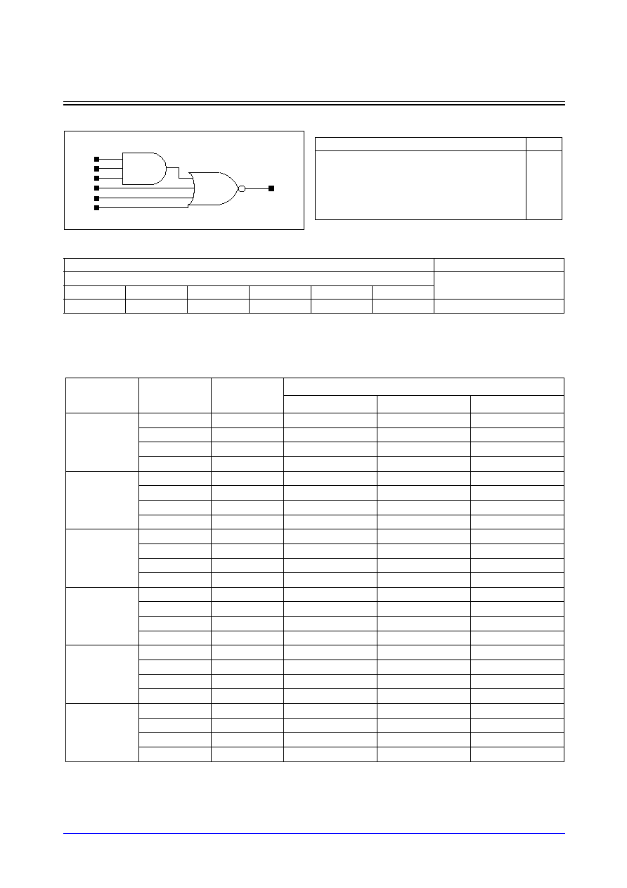
STDL131
3-112
Samsung ASIC
AO3111_LP
3-AND into 4-NOR with 1X Drive
Logic Symbol
Cell Data
Switching Characteristics
(Typical process, 25
∞
C, 1.8V, t
R
/t
F
= 0.19ns, SL: Standard Load)
AO3111_LP
Input Load (SL)
Gate Count
AO3111_LP
AO3111_LP
A
B
C
D
E
F
1.0
1.0
1.0
0.9
1.0
0.9
2.67
Truth Table
A
B
C
D
E
F
Y
1
1
1
x
x
x
0
x
x
x
1
x
x
0
x
x
x
x
1
x
0
x
x
x
x
x
1
0
Other States
1
Y
D
E
A
B
C
F
Path
Parameter
Delay [ns]
SL = 2
Delay Equations [ns]
Group1*
Group2*
Group3*
A to Y
tR
0.597
0.379 + 0.109*SL
0.373 + 0.110*SL
0.384 + 0.109*SL
tF
0.239
0.147 + 0.046*SL
0.142 + 0.047*SL
0.136 + 0.048*SL
tPLH
0.244
0.139 + 0.053*SL
0.137 + 0.053*SL
0.139 + 0.053*SL
tPHL
0.175
0.124 + 0.025*SL
0.125 + 0.025*SL
0.126 + 0.025*SL
B to Y
tR
0.626
0.408 + 0.109*SL
0.403 + 0.110*SL
0.414 + 0.109*SL
tF
0.237
0.144 + 0.047*SL
0.141 + 0.048*SL
0.136 + 0.048*SL
tPLH
0.270
0.163 + 0.053*SL
0.163 + 0.053*SL
0.165 + 0.053*SL
tPHL
0.178
0.127 + 0.025*SL
0.129 + 0.025*SL
0.130 + 0.025*SL
C to Y
tR
0.655
0.437 + 0.109*SL
0.432 + 0.110*SL
0.444 + 0.109*SL
tF
0.236
0.141 + 0.047*SL
0.139 + 0.048*SL
0.135 + 0.048*SL
tPLH
0.293
0.186 + 0.053*SL
0.187 + 0.053*SL
0.190 + 0.053*SL
tPHL
0.178
0.127 + 0.025*SL
0.129 + 0.025*SL
0.130 + 0.025*SL
D to Y
tR
0.694
0.482 + 0.106*SL
0.479 + 0.107*SL
0.477 + 0.107*SL
tF
0.283
0.199 + 0.042*SL
0.198 + 0.042*SL
0.197 + 0.042*SL
tPLH
0.447
0.340 + 0.053*SL
0.342 + 0.053*SL
0.344 + 0.053*SL
tPHL
0.257
0.209 + 0.024*SL
0.211 + 0.023*SL
0.214 + 0.023*SL
E to Y
tR
0.694
0.483 + 0.106*SL
0.480 + 0.107*SL
0.477 + 0.107*SL
tF
0.313
0.228 + 0.042*SL
0.227 + 0.042*SL
0.229 + 0.042*SL
tPLH
0.489
0.382 + 0.053*SL
0.384 + 0.053*SL
0.386 + 0.053*SL
tPHL
0.279
0.230 + 0.024*SL
0.233 + 0.024*SL
0.236 + 0.023*SL
F to Y
tR
0.694
0.483 + 0.106*SL
0.479 + 0.107*SL
0.477 + 0.107*SL
tF
0.340
0.253 + 0.043*SL
0.255 + 0.043*SL
0.258 + 0.042*SL
tPLH
0.506
0.399 + 0.053*SL
0.401 + 0.053*SL
0.403 + 0.053*SL
tPHL
0.293
0.243 + 0.025*SL
0.247 + 0.024*SL
0.252 + 0.024*SL
*Group1 : SL < 4, *Group2 : 4 SL
<
<
=
= 8, *Group3 : 8 < SL
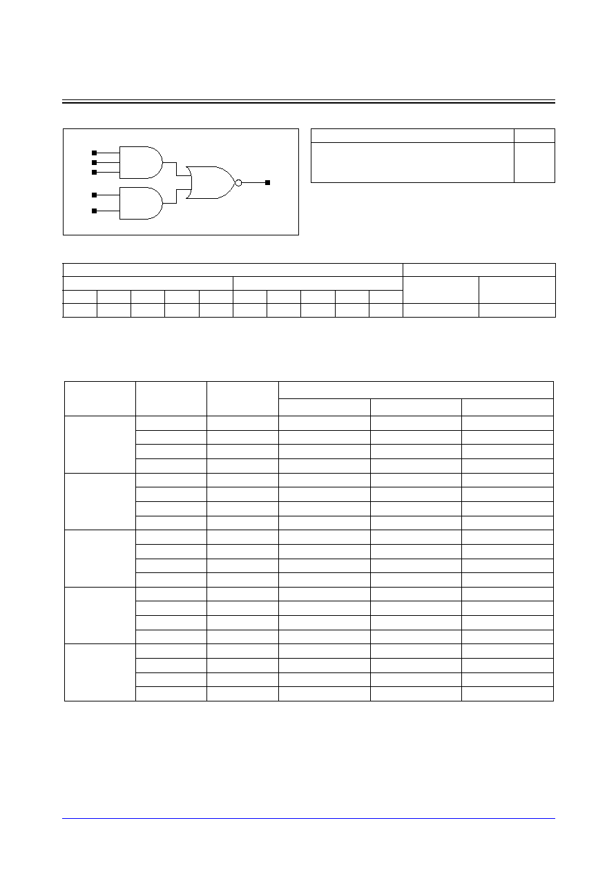
Samsung ASIC
3-113
STDL131
AO32_LP/AO32D2_LP
3-AND and 2-AND into 2-NOR with 1X/2X Drive
Logic Symbol
Cell Data
Switching Characteristics
(Typical process, 25
∞
C, 1.8V, t
R
/t
F
= 0.19ns, SL: Standard Load)
AO32_LP
Input Load (SL)
Gate Count
AO32_LP
AO32D2_LP
AO32_LP
AO32D2_LP
A
B
C
D
E
A
B
C
D
E
1.1
1.1
1.1
1.1
1.1
0.8
0.9
0.8
0.9
0.8
2.33
3.33
Y
A
B
C
D
E
Path
Parameter
Delay [ns]
SL = 2
Delay Equations [ns]
Group1*
Group2*
Group3*
A to Y
tR
0.278
0.175 + 0.051*SL
0.169 + 0.053*SL
0.163 + 0.054*SL
tF
0.224
0.142 + 0.041*SL
0.136 + 0.042*SL
0.129 + 0.043*SL
tPLH
0.174
0.122 + 0.026*SL
0.122 + 0.026*SL
0.123 + 0.026*SL
tPHL
0.151
0.105 + 0.023*SL
0.106 + 0.023*SL
0.107 + 0.023*SL
B to Y
tR
0.294
0.190 + 0.052*SL
0.184 + 0.053*SL
0.179 + 0.054*SL
tF
0.222
0.139 + 0.042*SL
0.135 + 0.043*SL
0.129 + 0.043*SL
tPLH
0.189
0.136 + 0.026*SL
0.136 + 0.026*SL
0.138 + 0.026*SL
tPHL
0.154
0.108 + 0.023*SL
0.110 + 0.023*SL
0.110 + 0.023*SL
C to Y
tR
0.309
0.204 + 0.052*SL
0.199 + 0.054*SL
0.194 + 0.054*SL
tF
0.219
0.135 + 0.042*SL
0.132 + 0.043*SL
0.128 + 0.043*SL
tPLH
0.201
0.147 + 0.027*SL
0.149 + 0.026*SL
0.150 + 0.026*SL
tPHL
0.154
0.108 + 0.023*SL
0.109 + 0.023*SL
0.110 + 0.023*SL
D to Y
tR
0.296
0.189 + 0.053*SL
0.187 + 0.054*SL
0.185 + 0.054*SL
tF
0.233
0.175 + 0.029*SL
0.172 + 0.030*SL
0.166 + 0.031*SL
tPLH
0.252
0.198 + 0.027*SL
0.200 + 0.026*SL
0.201 + 0.026*SL
tPHL
0.187
0.152 + 0.017*SL
0.155 + 0.017*SL
0.157 + 0.017*SL
E to Y
tR
0.310
0.203 + 0.053*SL
0.202 + 0.054*SL
0.200 + 0.054*SL
tF
0.230
0.171 + 0.030*SL
0.169 + 0.030*SL
0.165 + 0.031*SL
tPLH
0.266
0.212 + 0.027*SL
0.214 + 0.026*SL
0.215 + 0.026*SL
tPHL
0.184
0.150 + 0.017*SL
0.152 + 0.017*SL
0.155 + 0.017*SL
*Group1 : SL < 4, *Group2 : 4 SL
<
<
=
= 8, *Group3 : 8 < SL
Truth Table
A
B
C
D
E
Y
1
1
1
x
x
0
x
x
x
1
1
0
Other States
1

STDL131
3-114
Samsung ASIC
AO32_LP/AO32D2_LP
3-AND and 2-AND into 2-NOR with 1X/2X Drive
Switching Characteristics
(Typical process, 25
∞
C, 1.8V, t
R
/t
F
= 0.19ns, SL: Standard Load)
AO32D2_LP
Path
Parameter
Delay [ns]
SL = 2
Delay Equations [ns]
Group1*
Group2*
Group3*
A to Y
tR
0.065
0.043 + 0.011*SL
0.037 + 0.013*SL
0.031 + 0.013*SL
tF
0.057
0.041 + 0.008*SL
0.041 + 0.008*SL
0.036 + 0.008*SL
tPLH
0.285
0.269 + 0.008*SL
0.274 + 0.006*SL
0.276 + 0.006*SL
tPHL
0.315
0.301 + 0.007*SL
0.308 + 0.006*SL
0.316 + 0.005*SL
B to Y
tR
0.066
0.043 + 0.011*SL
0.038 + 0.013*SL
0.031 + 0.013*SL
tF
0.057
0.041 + 0.008*SL
0.041 + 0.008*SL
0.036 + 0.008*SL
tPLH
0.297
0.282 + 0.008*SL
0.286 + 0.006*SL
0.288 + 0.006*SL
tPHL
0.319
0.304 + 0.007*SL
0.311 + 0.006*SL
0.319 + 0.005*SL
C to Y
tR
0.064
0.040 + 0.012*SL
0.038 + 0.013*SL
0.032 + 0.013*SL
tF
0.056
0.041 + 0.008*SL
0.039 + 0.008*SL
0.036 + 0.008*SL
tPLH
0.308
0.293 + 0.008*SL
0.297 + 0.006*SL
0.300 + 0.006*SL
tPHL
0.318
0.304 + 0.007*SL
0.311 + 0.006*SL
0.319 + 0.005*SL
D to Y
tR
0.066
0.044 + 0.011*SL
0.038 + 0.013*SL
0.031 + 0.013*SL
tF
0.056
0.040 + 0.008*SL
0.041 + 0.008*SL
0.036 + 0.008*SL
tPLH
0.357
0.342 + 0.008*SL
0.347 + 0.006*SL
0.349 + 0.006*SL
tPHL
0.387
0.372 + 0.007*SL
0.379 + 0.006*SL
0.387 + 0.005*SL
E to Y
tR
0.066
0.043 + 0.011*SL
0.038 + 0.013*SL
0.031 + 0.013*SL
tF
0.056
0.038 + 0.009*SL
0.042 + 0.008*SL
0.037 + 0.008*SL
tPLH
0.369
0.353 + 0.008*SL
0.358 + 0.006*SL
0.360 + 0.006*SL
tPHL
0.385
0.370 + 0.007*SL
0.377 + 0.006*SL
0.384 + 0.005*SL
*Group1 : SL < 4, *Group2 : 4 SL
<
<
=
= 12, *Group3 : 12 < SL
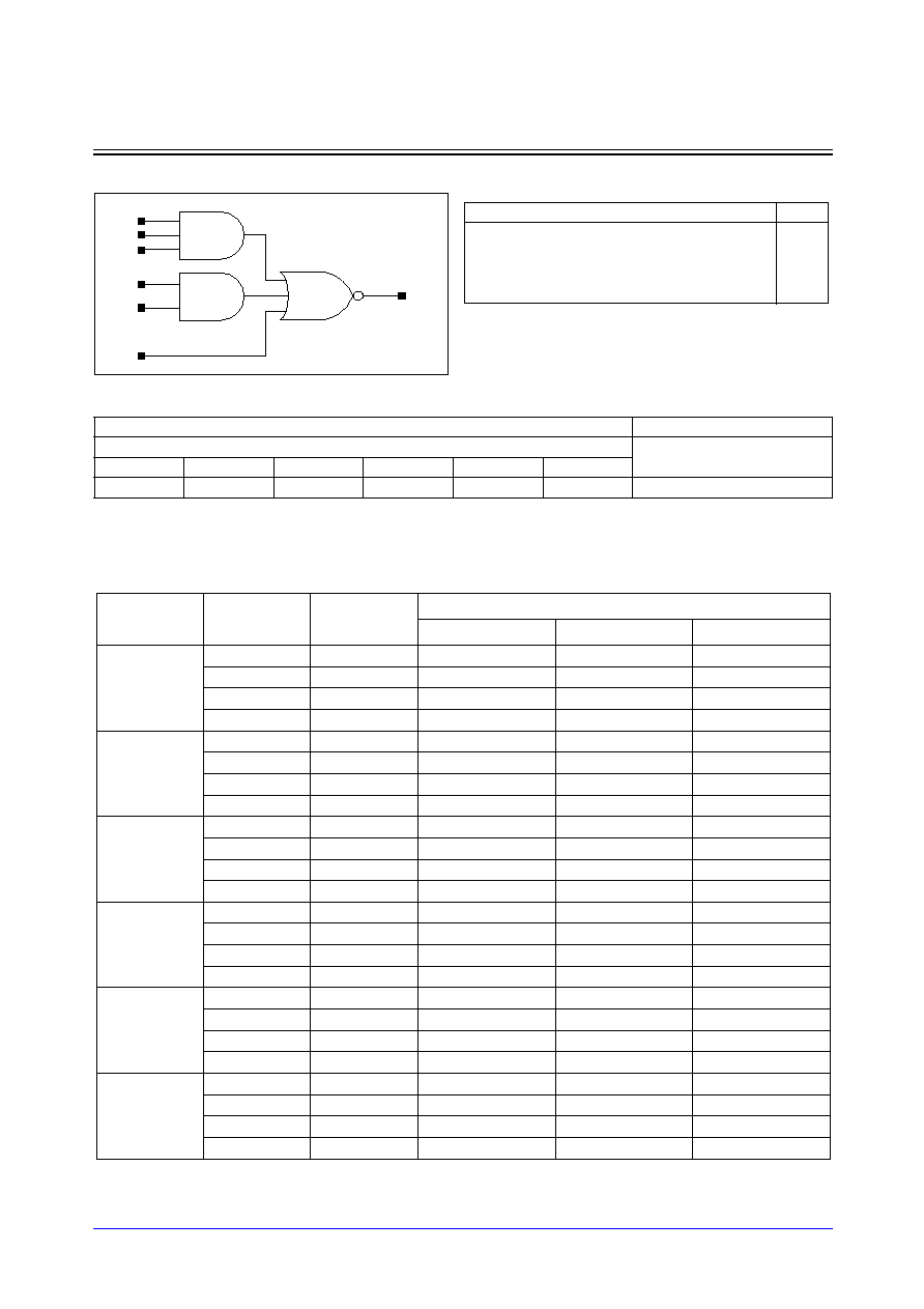
Samsung ASIC
3-115
STDL131
AO321_LP
3-AND and 2-AND into 3-NOR with 1X Drive
Logic Symbol
Cell Data
Switching Characteristics
(Typical process, 25
∞
C, 1.8V, t
R
/t
F
= 0.19ns, SL: Standard Load)
AO321_LP
Input Load (SL)
Gate Count
AO321_LP
AO321_LP
A
B
C
D
E
F
1.1
1.1
1.1
1.0
1.0
1.0
2.67
Truth Table
A
B
C
D
E
F
Y
1
1
1
x
x
x
0
x
x
x
1
1
x
0
x
x
x
x
x
1
0
Other States
1
A
B
C
D
E
Y
F
Path
Parameter
Delay [ns]
SL = 2
Delay Equations [ns]
Group1*
Group2*
Group3*
A to Y
tR
0.452
0.288 + 0.082*SL
0.282 + 0.084*SL
0.284 + 0.083*SL
tF
0.204
0.134 + 0.035*SL
0.128 + 0.036*SL
0.121 + 0.037*SL
tPLH
0.223
0.142 + 0.040*SL
0.142 + 0.041*SL
0.144 + 0.040*SL
tPHL
0.139
0.100 + 0.020*SL
0.101 + 0.019*SL
0.101 + 0.019*SL
B to Y
tR
0.479
0.314 + 0.083*SL
0.310 + 0.084*SL
0.313 + 0.083*SL
tF
0.200
0.129 + 0.036*SL
0.125 + 0.037*SL
0.120 + 0.037*SL
tPLH
0.248
0.167 + 0.041*SL
0.167 + 0.041*SL
0.169 + 0.040*SL
tPHL
0.143
0.103 + 0.020*SL
0.104 + 0.020*SL
0.105 + 0.019*SL
C to Y
tR
0.508
0.343 + 0.083*SL
0.338 + 0.084*SL
0.343 + 0.083*SL
tF
0.197
0.125 + 0.036*SL
0.122 + 0.037*SL
0.119 + 0.037*SL
tPLH
0.272
0.190 + 0.041*SL
0.191 + 0.041*SL
0.193 + 0.040*SL
tPHL
0.143
0.103 + 0.020*SL
0.104 + 0.020*SL
0.106 + 0.019*SL
D to Y
tR
0.509
0.347 + 0.081*SL
0.345 + 0.082*SL
0.342 + 0.082*SL
tF
0.245
0.178 + 0.033*SL
0.176 + 0.034*SL
0.171 + 0.035*SL
tPLH
0.374
0.292 + 0.041*SL
0.294 + 0.041*SL
0.296 + 0.040*SL
tPHL
0.209
0.170 + 0.020*SL
0.172 + 0.019*SL
0.175 + 0.019*SL
E to Y
tR
0.530
0.368 + 0.081*SL
0.366 + 0.082*SL
0.363 + 0.082*SL
tF
0.264
0.197 + 0.034*SL
0.194 + 0.034*SL
0.191 + 0.035*SL
tPLH
0.394
0.312 + 0.041*SL
0.314 + 0.041*SL
0.315 + 0.040*SL
tPHL
0.206
0.167 + 0.020*SL
0.170 + 0.019*SL
0.172 + 0.019*SL
F to Y
tR
0.531
0.368 + 0.081*SL
0.366 + 0.082*SL
0.363 + 0.082*SL
tF
0.275
0.212 + 0.031*SL
0.212 + 0.032*SL
0.210 + 0.032*SL
tPLH
0.428
0.346 + 0.041*SL
0.347 + 0.041*SL
0.349 + 0.040*SL
tPHL
0.212
0.173 + 0.020*SL
0.176 + 0.019*SL
0.181 + 0.018*SL
*Group1 : SL < 4, *Group2 : 4 SL
<
<
=
= 8, *Group3 : 8 < SL

STDL131
3-116
Samsung ASIC
AO322_LP
3-AND and Two 2-ANDs into 3-NOR with 1X Drive
Logic Symbol
Cell Data
Input Load (SL)
Gate Count
AO322_LP
AO322_LP
A
B
C
D
E
F
G
1.1
1.1
1.1
1.0
1.0
1.0
1.1
3.00
A
B
C
D
E
Y
F
G
Truth Table
A
B
C
D
E
F
G
Y
1
1
1
x
x
x
x
0
x
x
x
1
1
x
x
0
x
x
x
x
x
1
1
0
Other States
1
Samsung ASIC
3-117
STDL131
AO322_LP
3-AND and Two 2-ANDs into 3-NOR with 1X Drive
Switching Characteristics
(Typical process, 25
∞
C, 1.8V, t
R
/t
F
= 0.19ns, SL: Standard Load)
AO322_LP
Path
Parameter
Delay [ns]
SL = 2
Delay Equations [ns]
Group1*
Group2*
Group3*
A to Y
tR
0.480
0.314 + 0.083*SL
0.310 + 0.084*SL
0.314 + 0.084*SL
tF
0.220
0.150 + 0.035*SL
0.145 + 0.036*SL
0.138 + 0.037*SL
tPLH
0.244
0.162 + 0.041*SL
0.162 + 0.041*SL
0.164 + 0.040*SL
tPHL
0.141
0.102 + 0.020*SL
0.103 + 0.019*SL
0.103 + 0.019*SL
B to Y
tR
0.507
0.341 + 0.083*SL
0.337 + 0.084*SL
0.342 + 0.083*SL
tF
0.217
0.145 + 0.036*SL
0.142 + 0.037*SL
0.138 + 0.037*SL
tPLH
0.268
0.187 + 0.041*SL
0.187 + 0.041*SL
0.189 + 0.040*SL
tPHL
0.145
0.105 + 0.020*SL
0.106 + 0.020*SL
0.108 + 0.019*SL
C to Y
tR
0.535
0.369 + 0.083*SL
0.366 + 0.084*SL
0.372 + 0.083*SL
tF
0.214
0.141 + 0.037*SL
0.139 + 0.037*SL
0.136 + 0.037*SL
tPLH
0.291
0.210 + 0.041*SL
0.211 + 0.041*SL
0.213 + 0.040*SL
tPHL
0.145
0.105 + 0.020*SL
0.107 + 0.020*SL
0.107 + 0.019*SL
D to Y
tR
0.540
0.377 + 0.081*SL
0.375 + 0.082*SL
0.373 + 0.082*SL
tF
0.274
0.205 + 0.035*SL
0.203 + 0.035*SL
0.199 + 0.036*SL
tPLH
0.396
0.314 + 0.041*SL
0.316 + 0.041*SL
0.318 + 0.040*SL
tPHL
0.204
0.164 + 0.020*SL
0.166 + 0.019*SL
0.169 + 0.019*SL
E to Y
tR
0.559
0.396 + 0.081*SL
0.395 + 0.082*SL
0.393 + 0.082*SL
tF
0.273
0.203 + 0.035*SL
0.202 + 0.035*SL
0.199 + 0.036*SL
tPLH
0.414
0.333 + 0.041*SL
0.334 + 0.040*SL
0.336 + 0.040*SL
tPHL
0.201
0.161 + 0.020*SL
0.163 + 0.020*SL
0.166 + 0.019*SL
F to Y
tR
0.539
0.377 + 0.081*SL
0.375 + 0.082*SL
0.373 + 0.082*SL
tF
0.326
0.255 + 0.036*SL
0.255 + 0.036*SL
0.252 + 0.036*SL
tPLH
0.447
0.365 + 0.041*SL
0.366 + 0.041*SL
0.369 + 0.040*SL
tPHL
0.231
0.188 + 0.022*SL
0.192 + 0.021*SL
0.198 + 0.020*SL
G to Y
tR
0.559
0.397 + 0.081*SL
0.395 + 0.082*SL
0.393 + 0.082*SL
tF
0.326
0.254 + 0.036*SL
0.254 + 0.036*SL
0.254 + 0.036*SL
tPLH
0.465
0.383 + 0.041*SL
0.385 + 0.040*SL
0.387 + 0.040*SL
tPHL
0.228
0.185 + 0.022*SL
0.190 + 0.020*SL
0.195 + 0.020*SL
*Group1 : SL < 4, *Group2 : 4 SL
<
<
=
= 8, *Group3 : 8 < SL
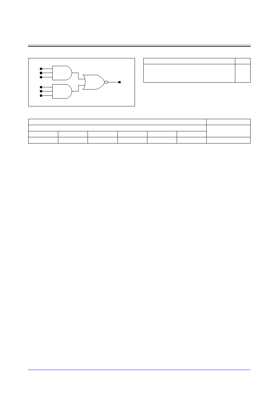
STDL131
3-118
Samsung ASIC
AO33_LP
Two 3-ANDs into 2-NOR with 1X Drive
Logic Symbol
Cell Data
Input Load (SL)
Gate Count
AO33_LP
AO33_LP
A
B
C
D
E
F
1.1
1.1
1.1
1.1
1.1
1.1
2.67
Y
A
B
C
D
E
F
Truth Table
A
B
C
D
E
F
Y
1
1
1
x
x
x
0
x
x
x
1
1
1
0
Other States
1

Samsung ASIC
3-119
STDL131
AO33_LP
Two 3-ANDs into 2-NOR with 1X Drive
Switching Characteristics
(Typical process, 25
∞
C, 1.8V, t
R
/t
F
= 0.19ns, SL: Standard Load)
AO33_LP
Path
Parameter
Delay [ns]
SL = 2
Delay Equations [ns]
Group1*
Group2*
Group3*
A to Y
tR
0.293
0.189 + 0.052*SL
0.183 + 0.054*SL
0.178 + 0.054*SL
tF
0.224
0.142 + 0.041*SL
0.135 + 0.042*SL
0.128 + 0.043*SL
tPLH
0.188
0.134 + 0.027*SL
0.136 + 0.026*SL
0.137 + 0.026*SL
tPHL
0.149
0.103 + 0.023*SL
0.104 + 0.023*SL
0.105 + 0.023*SL
B to Y
tR
0.308
0.202 + 0.053*SL
0.197 + 0.054*SL
0.193 + 0.055*SL
tF
0.221
0.138 + 0.042*SL
0.134 + 0.043*SL
0.128 + 0.043*SL
tPLH
0.202
0.148 + 0.027*SL
0.150 + 0.026*SL
0.151 + 0.026*SL
tPHL
0.152
0.106 + 0.023*SL
0.108 + 0.023*SL
0.109 + 0.023*SL
C to Y
tR
0.322
0.216 + 0.053*SL
0.212 + 0.054*SL
0.208 + 0.054*SL
tF
0.218
0.134 + 0.042*SL
0.131 + 0.043*SL
0.127 + 0.043*SL
tPLH
0.214
0.160 + 0.027*SL
0.162 + 0.027*SL
0.164 + 0.026*SL
tPHL
0.152
0.106 + 0.023*SL
0.107 + 0.023*SL
0.108 + 0.023*SL
D to Y
tR
0.297
0.189 + 0.054*SL
0.187 + 0.054*SL
0.185 + 0.055*SL
tF
0.323
0.239 + 0.042*SL
0.235 + 0.043*SL
0.229 + 0.044*SL
tPLH
0.256
0.201 + 0.027*SL
0.203 + 0.027*SL
0.205 + 0.027*SL
tPHL
0.242
0.194 + 0.024*SL
0.197 + 0.023*SL
0.200 + 0.023*SL
E to Y
tR
0.311
0.204 + 0.054*SL
0.202 + 0.054*SL
0.200 + 0.055*SL
tF
0.321
0.236 + 0.043*SL
0.235 + 0.043*SL
0.230 + 0.043*SL
tPLH
0.270
0.216 + 0.027*SL
0.218 + 0.027*SL
0.219 + 0.026*SL
tPHL
0.247
0.199 + 0.024*SL
0.202 + 0.023*SL
0.205 + 0.023*SL
F to Y
tR
0.325
0.218 + 0.053*SL
0.216 + 0.054*SL
0.215 + 0.054*SL
tF
0.321
0.236 + 0.043*SL
0.234 + 0.043*SL
0.231 + 0.043*SL
tPLH
0.282
0.228 + 0.027*SL
0.230 + 0.027*SL
0.231 + 0.026*SL
tPHL
0.248
0.200 + 0.024*SL
0.203 + 0.023*SL
0.206 + 0.023*SL
*Group1 : SL < 4, *Group2 : 4 SL
<
<
=
= 8, *Group3 : 8 < SL
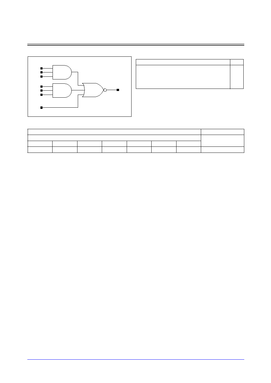
STDL131
3-120
Samsung ASIC
AO331_LP
Two 3-ANDs into 3-NOR with 1X Drive
Logic Symbol
Cell Data
Input Load (SL)
Gate Count
AO331_LP
AO331_LP
A
B
C
D
E
F
G
1.1
1.1
1.1
1.1
1.1
1.1
1.0
3.00
Truth Table
A
B
C
D
E
F
G
Y
1
1
1
x
x
x
x
0
x
x
x
1
1
1
x
0
x
x
x
x
x
x
1
0
Other States
1
A
B
C
Y
G
D
E
F
Samsung ASIC
3-121
STDL131
AO331_LP
Two 3-ANDs into 3-NOR with 1X Drive
Switching Characteristics
(Typical process, 25
∞
C, 1.8V, t
R
/t
F
= 0.19ns, SL: Standard Load)
AO331_LP
Path
Parameter
Delay [ns]
SL = 2
Delay Equations [ns]
Group1*
Group2*
Group3*
A to Y
tR
0.473
0.310 + 0.081*SL
0.305 + 0.083*SL
0.307 + 0.082*SL
tF
0.231
0.148 + 0.041*SL
0.143 + 0.042*SL
0.136 + 0.043*SL
tPLH
0.234
0.154 + 0.040*SL
0.154 + 0.040*SL
0.156 + 0.040*SL
tPHL
0.155
0.109 + 0.023*SL
0.110 + 0.023*SL
0.111 + 0.023*SL
B to Y
tR
0.496
0.332 + 0.082*SL
0.328 + 0.083*SL
0.331 + 0.082*SL
tF
0.228
0.145 + 0.042*SL
0.141 + 0.043*SL
0.136 + 0.043*SL
tPLH
0.255
0.175 + 0.040*SL
0.175 + 0.040*SL
0.177 + 0.040*SL
tPHL
0.158
0.112 + 0.023*SL
0.113 + 0.023*SL
0.114 + 0.023*SL
C to Y
tR
0.518
0.355 + 0.082*SL
0.351 + 0.083*SL
0.355 + 0.082*SL
tF
0.226
0.141 + 0.042*SL
0.139 + 0.043*SL
0.135 + 0.043*SL
tPLH
0.274
0.193 + 0.040*SL
0.194 + 0.040*SL
0.196 + 0.040*SL
tPHL
0.157
0.111 + 0.023*SL
0.112 + 0.023*SL
0.114 + 0.023*SL
D to Y
tR
0.504
0.345 + 0.079*SL
0.341 + 0.080*SL
0.338 + 0.081*SL
tF
0.335
0.250 + 0.042*SL
0.246 + 0.043*SL
0.242 + 0.044*SL
tPLH
0.373
0.291 + 0.041*SL
0.294 + 0.040*SL
0.296 + 0.040*SL
tPHL
0.254
0.206 + 0.024*SL
0.209 + 0.023*SL
0.212 + 0.023*SL
E to Y
tR
0.526
0.367 + 0.080*SL
0.364 + 0.080*SL
0.361 + 0.081*SL
tF
0.335
0.249 + 0.043*SL
0.247 + 0.043*SL
0.243 + 0.044*SL
tPLH
0.395
0.314 + 0.040*SL
0.316 + 0.040*SL
0.318 + 0.040*SL
tPHL
0.259
0.210 + 0.024*SL
0.213 + 0.023*SL
0.217 + 0.023*SL
F to Y
tR
0.549
0.389 + 0.080*SL
0.387 + 0.080*SL
0.384 + 0.081*SL
tF
0.334
0.248 + 0.043*SL
0.247 + 0.043*SL
0.243 + 0.044*SL
tPLH
0.415
0.334 + 0.040*SL
0.336 + 0.040*SL
0.338 + 0.040*SL
tPHL
0.259
0.211 + 0.024*SL
0.214 + 0.023*SL
0.217 + 0.023*SL
G to Y
tR
0.549
0.390 + 0.080*SL
0.387 + 0.080*SL
0.384 + 0.081*SL
tF
0.309
0.242 + 0.033*SL
0.241 + 0.034*SL
0.240 + 0.034*SL
tPLH
0.462
0.381 + 0.040*SL
0.383 + 0.040*SL
0.385 + 0.040*SL
tPHL
0.233
0.190 + 0.021*SL
0.195 + 0.020*SL
0.201 + 0.019*SL
*Group1 : SL < 4, *Group2 : 4 SL
<
<
=
= 8, *Group3 : 8 < SL
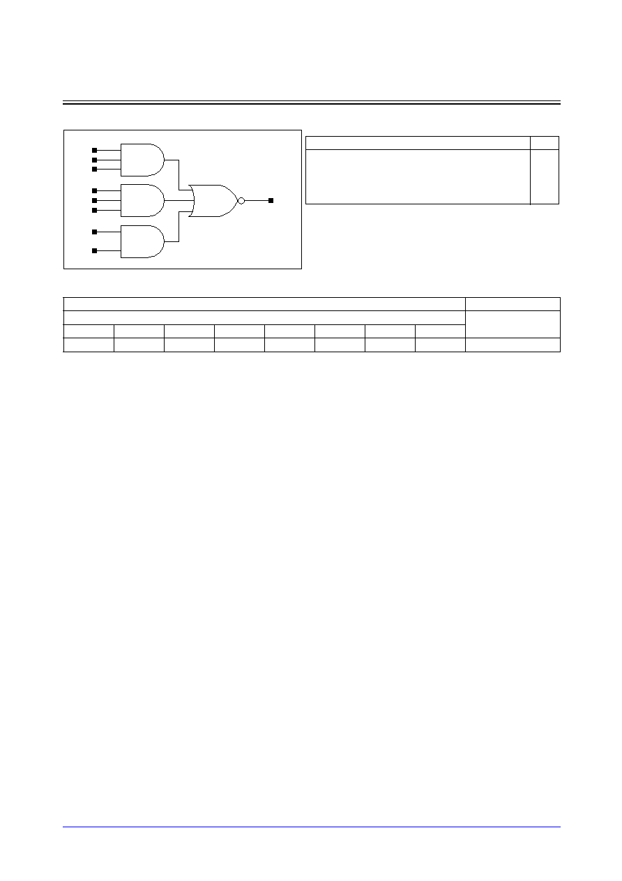
STDL131
3-122
Samsung ASIC
AO332_LP
Two 3-ANDs and 2-AND into 3-NOR with 1X Drive
Logic Symbol
Cell Data
Input Load (SL)
Gate Count
AO332_LP
AO332_LP
A
B
C
D
E
F
G
H
1.1
1.1
1.1
1.1
1.1
1.1
1.0
1.1
3.33
Truth Table
A
B
C
D
E
F
G
H
Y
1
1
1
x
x
x
x
x
0
x
x
x
1
1
1
x
x
0
x
x
x
x
x
x
1
1
0
Other States
1
D
F
A
C
Y
G
H
E
B
Samsung ASIC
3-123
STDL131
AO332_LP
Two 3-ANDs and 2-AND into 3-NOR with 1X Drive
Switching Characteristics
(Typical process, 25
∞
C, 1.8V, t
R
/t
F
= 0.19ns, SL: Standard Load)
AO332_LP
Path
Parameter
Delay [ns]
SL = 2
Delay Equations [ns]
Group1*
Group2*
Group3*
A to Y
tR
0.483
0.319 + 0.082*SL
0.315 + 0.083*SL
0.317 + 0.083*SL
tF
0.252
0.170 + 0.041*SL
0.165 + 0.042*SL
0.157 + 0.043*SL
tPLH
0.239
0.159 + 0.040*SL
0.158 + 0.040*SL
0.161 + 0.040*SL
tPHL
0.157
0.111 + 0.023*SL
0.113 + 0.023*SL
0.113 + 0.023*SL
B to Y
tR
0.507
0.342 + 0.082*SL
0.338 + 0.083*SL
0.342 + 0.083*SL
tF
0.250
0.166 + 0.042*SL
0.162 + 0.043*SL
0.157 + 0.043*SL
tPLH
0.260
0.179 + 0.040*SL
0.180 + 0.040*SL
0.182 + 0.040*SL
tPHL
0.161
0.115 + 0.023*SL
0.115 + 0.023*SL
0.117 + 0.023*SL
C to Y
tR
0.530
0.365 + 0.082*SL
0.361 + 0.083*SL
0.365 + 0.083*SL
tF
0.247
0.163 + 0.042*SL
0.160 + 0.043*SL
0.157 + 0.043*SL
tPLH
0.279
0.198 + 0.041*SL
0.199 + 0.040*SL
0.201 + 0.040*SL
tPHL
0.160
0.113 + 0.023*SL
0.115 + 0.023*SL
0.116 + 0.023*SL
D to Y
tR
0.537
0.376 + 0.081*SL
0.373 + 0.081*SL
0.371 + 0.082*SL
tF
0.345
0.258 + 0.044*SL
0.255 + 0.044*SL
0.253 + 0.045*SL
tPLH
0.396
0.313 + 0.041*SL
0.316 + 0.041*SL
0.318 + 0.040*SL
tPHL
0.243
0.194 + 0.025*SL
0.196 + 0.024*SL
0.200 + 0.024*SL
E to Y
tR
0.560
0.398 + 0.081*SL
0.396 + 0.081*SL
0.394 + 0.082*SL
tF
0.346
0.258 + 0.044*SL
0.257 + 0.044*SL
0.254 + 0.045*SL
tPLH
0.418
0.336 + 0.041*SL
0.338 + 0.040*SL
0.340 + 0.040*SL
tPHL
0.247
0.197 + 0.025*SL
0.201 + 0.024*SL
0.204 + 0.024*SL
F to Y
tR
0.580
0.419 + 0.081*SL
0.417 + 0.081*SL
0.415 + 0.081*SL
tF
0.345
0.257 + 0.044*SL
0.256 + 0.044*SL
0.254 + 0.045*SL
tPLH
0.436
0.355 + 0.041*SL
0.356 + 0.040*SL
0.358 + 0.040*SL
tPHL
0.248
0.199 + 0.025*SL
0.202 + 0.024*SL
0.205 + 0.024*SL
G to Y
tR
0.561
0.400 + 0.080*SL
0.397 + 0.081*SL
0.395 + 0.081*SL
tF
0.347
0.275 + 0.036*SL
0.274 + 0.036*SL
0.273 + 0.036*SL
tPLH
0.478
0.396 + 0.041*SL
0.399 + 0.040*SL
0.401 + 0.040*SL
tPHL
0.241
0.196 + 0.022*SL
0.201 + 0.021*SL
0.208 + 0.020*SL
H to Y
tR
0.580
0.420 + 0.080*SL
0.417 + 0.081*SL
0.415 + 0.081*SL
tF
0.347
0.274 + 0.036*SL
0.275 + 0.036*SL
0.274 + 0.036*SL
tPLH
0.497
0.415 + 0.041*SL
0.417 + 0.040*SL
0.419 + 0.040*SL
tPHL
0.238
0.193 + 0.022*SL
0.198 + 0.021*SL
0.205 + 0.020*SL
*Group1 : SL < 4, *Group2 : 4 SL
<
<
=
= 8, *Group3 : 8 < SL
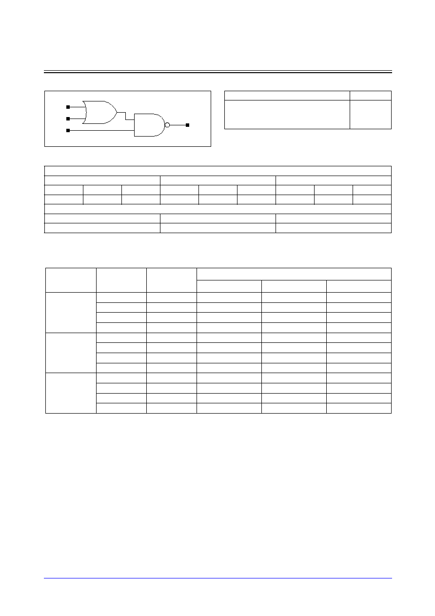
STDL131
3-124
Samsung ASIC
OA21_LP/OA21D2_LP/OA21D4_LP
2-OR into 2-NAND with 1X/2X/4X Drive
Logic Symbol
Cell Data
Switching Characteristics
(Typical process, 25
∞
C, 1.8V, t
R
/t
F
= 0.19ns, SL: Standard Load)
OA21_LP
Input Load (SL)
OA21_LP
OA21D2_LP
OA21D4_LP
A
B
C
A
B
C
A
B
C
1.1
1.1
1.1
2.2
2.1
2.2
1.0
0.9
1.0
Gate Count
OA21_LP
OA21D2_LP
OA21D4_LP
1.33
2.33
3.00
Y
C
A
B
Path
Parameter
Delay [ns]
SL = 2
Delay Equations [ns]
Group1*
Group2*
Group3*
A to Y
tR
0.220
0.119 + 0.051*SL
0.110 + 0.053*SL
0.100 + 0.054*SL
tF
0.137
0.080 + 0.029*SL
0.071 + 0.031*SL
0.063 + 0.032*SL
tPLH
0.150
0.097 + 0.026*SL
0.097 + 0.026*SL
0.098 + 0.026*SL
tPHL
0.111
0.074 + 0.018*SL
0.079 + 0.017*SL
0.079 + 0.017*SL
B to Y
tR
0.212
0.106 + 0.053*SL
0.102 + 0.054*SL
0.099 + 0.054*SL
tF
0.162
0.102 + 0.030*SL
0.097 + 0.031*SL
0.088 + 0.032*SL
tPLH
0.170
0.116 + 0.027*SL
0.117 + 0.026*SL
0.118 + 0.026*SL
tPHL
0.131
0.095 + 0.018*SL
0.097 + 0.017*SL
0.099 + 0.017*SL
C to Y
tR
0.134
0.087 + 0.023*SL
0.081 + 0.025*SL
0.071 + 0.026*SL
tF
0.153
0.091 + 0.031*SL
0.088 + 0.032*SL
0.084 + 0.032*SL
tPLH
0.118
0.092 + 0.013*SL
0.094 + 0.013*SL
0.094 + 0.013*SL
tPHL
0.136
0.100 + 0.018*SL
0.102 + 0.018*SL
0.104 + 0.017*SL
*Group1 : SL < 4, *Group2 : 4 SL
<
<
=
= 8, *Group3 : 8 < SL
Truth Table
A
B
C
Y
0
0
x
1
x
x
0
1
Others States
0

Samsung ASIC
3-125
STDL131
OA21_LP/OA21D2_LP/OA21D4_LP
2-OR into 2-NAND with 1X/2X/4X Drive
Switching Characteristics
(Typical process, 25
∞
C, 1.8V, t
R
/t
F
= 0.19ns, SL: Standard Load)
OA21D2_LP
OA21D4_LP
Path
Parameter
Delay [ns]
SL = 2
Delay Equations [ns]
Group1*
Group2*
Group3*
A to Y
tR
0.170
0.121 + 0.024*SL
0.116 + 0.026*SL
0.101 + 0.027*SL
tF
0.109
0.081 + 0.014*SL
0.077 + 0.015*SL
0.065 + 0.016*SL
tPLH
0.122
0.096 + 0.013*SL
0.096 + 0.013*SL
0.097 + 0.013*SL
tPHL
0.092
0.071 + 0.010*SL
0.078 + 0.009*SL
0.079 + 0.008*SL
B to Y
tR
0.159
0.108 + 0.025*SL
0.104 + 0.027*SL
0.098 + 0.027*SL
tF
0.132
0.104 + 0.014*SL
0.099 + 0.015*SL
0.090 + 0.016*SL
tPLH
0.142
0.115 + 0.013*SL
0.116 + 0.013*SL
0.117 + 0.013*SL
tPHL
0.113
0.095 + 0.009*SL
0.097 + 0.009*SL
0.099 + 0.009*SL
C to Y
tR
0.110
0.089 + 0.010*SL
0.082 + 0.012*SL
0.073 + 0.013*SL
tF
0.124
0.094 + 0.015*SL
0.091 + 0.016*SL
0.085 + 0.016*SL
tPLH
0.104
0.089 + 0.007*SL
0.093 + 0.006*SL
0.093 + 0.006*SL
tPHL
0.117
0.098 + 0.009*SL
0.100 + 0.009*SL
0.103 + 0.009*SL
*Group1 : SL < 4, *Group2 : 4 SL
<
<
=
= 12, *Group3 : 12 < SL
Path
Parameter
Delay [ns]
SL = 2
Delay Equations [ns]
Group1*
Group2*
Group3*
A to Y
tR
0.064
0.053 + 0.006*SL
0.051 + 0.006*SL
0.043 + 0.006*SL
tF
0.054
0.045 + 0.005*SL
0.047 + 0.004*SL
0.049 + 0.004*SL
tPLH
0.293
0.284 + 0.005*SL
0.289 + 0.004*SL
0.297 + 0.003*SL
tPHL
0.241
0.232 + 0.005*SL
0.237 + 0.003*SL
0.251 + 0.003*SL
B to Y
tR
0.065
0.054 + 0.006*SL
0.053 + 0.006*SL
0.044 + 0.006*SL
tF
0.056
0.047 + 0.005*SL
0.048 + 0.004*SL
0.050 + 0.004*SL
tPLH
0.314
0.304 + 0.005*SL
0.310 + 0.004*SL
0.318 + 0.003*SL
tPHL
0.261
0.252 + 0.005*SL
0.258 + 0.003*SL
0.272 + 0.003*SL
C to Y
tR
0.062
0.048 + 0.007*SL
0.052 + 0.006*SL
0.043 + 0.006*SL
tF
0.056
0.046 + 0.005*SL
0.049 + 0.004*SL
0.049 + 0.004*SL
tPLH
0.257
0.248 + 0.005*SL
0.253 + 0.004*SL
0.261 + 0.003*SL
tPHL
0.264
0.255 + 0.005*SL
0.261 + 0.003*SL
0.274 + 0.003*SL
*Group1 : SL < 4, *Group2 : 4 SL
<
<
=
= 20, *Group3 : 20 < SL
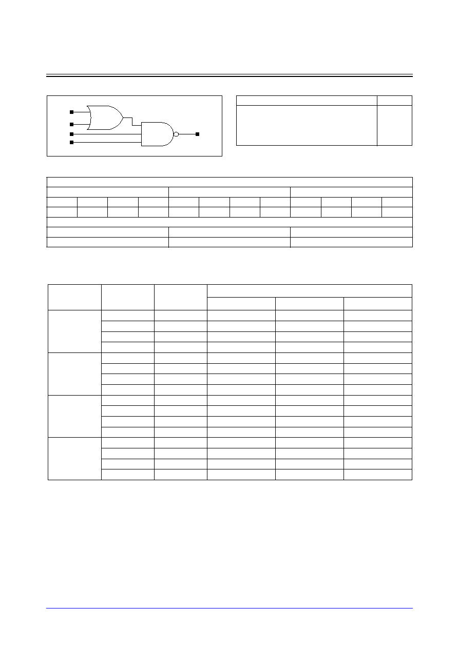
STDL131
3-126
Samsung ASIC
OA211_LP/OA211D2_LP/OA211D4_LP
2-OR into 3-NAND with 1X/2X/4X Drive
Logic Symbol
Cell Data
Switching Characteristics
(Typical process, 25
∞
C, 1.8V, t
R
/t
F
= 0.19ns, SL: Standard Load)
OA211_LP
Input Load (SL)
OA211_LP
OA211D2_LP
OA211D4_LP
A
B
C
D
A
B
C
D
A
B
C
D
1.1
1.1
0.9
0.9
2.2
2.2
1.8
1.8
0.9
0.9
0.9
0.9
Gate Count
OA211_LP
OA211D2_LP
OA211D4_LP
1.67
3.00
3.33
Y
C
A
B
D
Path
Parameter
Delay [ns]
SL = 2
Delay Equations [ns]
Group1*
Group2*
Group3*
A to Y
tR
0.240
0.139 + 0.050*SL
0.131 + 0.052*SL
0.122 + 0.054*SL
tF
0.176
0.106 + 0.035*SL
0.099 + 0.037*SL
0.091 + 0.038*SL
tPLH
0.161
0.109 + 0.026*SL
0.109 + 0.026*SL
0.110 + 0.026*SL
tPHL
0.128
0.088 + 0.020*SL
0.089 + 0.020*SL
0.090 + 0.020*SL
B to Y
tR
0.233
0.128 + 0.052*SL
0.125 + 0.053*SL
0.122 + 0.054*SL
tF
0.203
0.131 + 0.036*SL
0.126 + 0.037*SL
0.119 + 0.038*SL
tPLH
0.179
0.127 + 0.026*SL
0.128 + 0.026*SL
0.128 + 0.026*SL
tPHL
0.149
0.108 + 0.020*SL
0.110 + 0.020*SL
0.112 + 0.020*SL
C to Y
tR
0.189
0.119 + 0.035*SL
0.113 + 0.036*SL
0.104 + 0.038*SL
tF
0.197
0.124 + 0.037*SL
0.121 + 0.038*SL
0.117 + 0.038*SL
tPLH
0.154
0.118 + 0.018*SL
0.119 + 0.018*SL
0.120 + 0.018*SL
tPHL
0.160
0.119 + 0.021*SL
0.121 + 0.020*SL
0.123 + 0.020*SL
D to Y
tR
0.199
0.129 + 0.035*SL
0.123 + 0.037*SL
0.116 + 0.038*SL
tF
0.195
0.120 + 0.037*SL
0.119 + 0.038*SL
0.116 + 0.038*SL
tPLH
0.163
0.127 + 0.018*SL
0.128 + 0.018*SL
0.129 + 0.018*SL
tPHL
0.159
0.118 + 0.021*SL
0.120 + 0.020*SL
0.122 + 0.020*SL
*Group1 : SL < 4, *Group2 : 4 SL
<
<
=
= 8, *Group3 : 8 < SL
Truth Table
A
B
C
D
Y
0
0
x
x
1
x
x
0
x
1
x
x
x
0
1
Other States
0

Samsung ASIC
3-127
STDL131
OA211_LP/OA211D2_LP/OA211D4_LP
2-OR into 3-NAND with 1X/2X/4X Drive
Switching Characteristics
(Typical process, 25
∞
C, 1.8V, t
R
/t
F
= 0.19ns, SL: Standard Load)
OA211D2_LP
OA211D4_LP
Path
Parameter
Delay [ns]
SL = 2
Delay Equations [ns]
Group1*
Group2*
Group3*
A to Y
tR
0.189
0.139 + 0.025*SL
0.136 + 0.026*SL
0.124 + 0.027*SL
tF
0.140
0.106 + 0.017*SL
0.102 + 0.018*SL
0.092 + 0.019*SL
tPLH
0.134
0.108 + 0.013*SL
0.108 + 0.013*SL
0.109 + 0.013*SL
tPHL
0.106
0.086 + 0.010*SL
0.088 + 0.010*SL
0.089 + 0.010*SL
B to Y
tR
0.180
0.129 + 0.026*SL
0.126 + 0.026*SL
0.122 + 0.027*SL
tF
0.166
0.131 + 0.017*SL
0.127 + 0.018*SL
0.121 + 0.019*SL
tPLH
0.153
0.126 + 0.013*SL
0.127 + 0.013*SL
0.128 + 0.013*SL
tPHL
0.128
0.108 + 0.010*SL
0.109 + 0.010*SL
0.111 + 0.010*SL
C to Y
tR
0.154
0.120 + 0.017*SL
0.116 + 0.018*SL
0.107 + 0.019*SL
tF
0.160
0.124 + 0.018*SL
0.121 + 0.019*SL
0.118 + 0.019*SL
tPLH
0.137
0.119 + 0.009*SL
0.119 + 0.009*SL
0.120 + 0.009*SL
tPHL
0.139
0.118 + 0.010*SL
0.120 + 0.010*SL
0.122 + 0.010*SL
D to Y
tR
0.164
0.130 + 0.017*SL
0.127 + 0.018*SL
0.117 + 0.019*SL
tF
0.157
0.121 + 0.018*SL
0.119 + 0.019*SL
0.117 + 0.019*SL
tPLH
0.145
0.127 + 0.009*SL
0.128 + 0.009*SL
0.129 + 0.009*SL
tPHL
0.138
0.118 + 0.010*SL
0.119 + 0.010*SL
0.121 + 0.010*SL
*Group1 : SL < 4, *Group2 : 4 SL
<
<
=
= 12, *Group3 : 12 < SL
Path
Parameter
Delay [ns]
SL = 2
Delay Equations [ns]
Group1*
Group2*
Group3*
A to Y
tR
0.066
0.054 + 0.006*SL
0.055 + 0.006*SL
0.046 + 0.006*SL
tF
0.057
0.047 + 0.005*SL
0.051 + 0.004*SL
0.050 + 0.004*SL
tPLH
0.321
0.311 + 0.005*SL
0.317 + 0.004*SL
0.326 + 0.003*SL
tPHL
0.296
0.286 + 0.005*SL
0.292 + 0.003*SL
0.307 + 0.003*SL
B to Y
tR
0.067
0.055 + 0.006*SL
0.055 + 0.006*SL
0.043 + 0.006*SL
tF
0.058
0.049 + 0.005*SL
0.051 + 0.004*SL
0.052 + 0.004*SL
tPLH
0.340
0.330 + 0.005*SL
0.336 + 0.004*SL
0.345 + 0.003*SL
tPHL
0.323
0.313 + 0.005*SL
0.319 + 0.003*SL
0.334 + 0.003*SL
C to Y
tR
0.064
0.052 + 0.006*SL
0.053 + 0.006*SL
0.043 + 0.006*SL
tF
0.058
0.049 + 0.005*SL
0.051 + 0.004*SL
0.052 + 0.004*SL
tPLH
0.272
0.262 + 0.005*SL
0.268 + 0.004*SL
0.276 + 0.003*SL
tPHL
0.335
0.325 + 0.005*SL
0.332 + 0.003*SL
0.346 + 0.003*SL
D to Y
tR
0.063
0.050 + 0.006*SL
0.052 + 0.006*SL
0.044 + 0.006*SL
tF
0.058
0.049 + 0.005*SL
0.051 + 0.004*SL
0.052 + 0.004*SL
tPLH
0.278
0.268 + 0.005*SL
0.274 + 0.004*SL
0.282 + 0.003*SL
tPHL
0.334
0.324 + 0.005*SL
0.331 + 0.003*SL
0.346 + 0.003*SL
*Group1 : SL < 4, *Group2 : 4 SL
<
<
=
= 20, *Group3 : 20 < SL
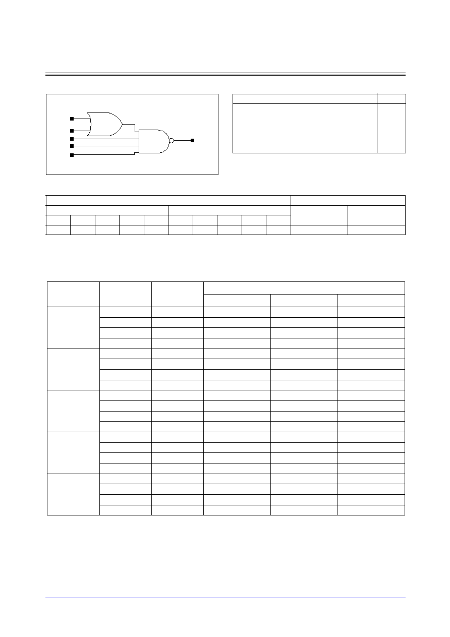
STDL131
3-128
Samsung ASIC
OA2111_LP/OA2111D2_LP
2-OR into 4-NAND with 1X/2X Drive
Logic Symbol
Cell Data
Switching Characteristics
(Typical process, 25
∞
C, 1.8V, t
R
/t
F
= 0.19ns, SL: Standard Load)
OA2111_LP
Input Load (SL)
Gate Count
OA2111_LP
OA2111D2_LP
OA2111_LP
OA2111D2_LP
A
B
C
D
E
A
B
C
D
E
1.1
1.1
0.9
0.9
0.9
2.1
2.3
1.8
1.8
1.8
2.00
3.67
Y
C
D
A
B
E
Path
Parameter
Delay [ns]
SL = 2
Delay Equations [ns]
Group1*
Group2*
Group3*
A to Y
tR
0.250
0.149 + 0.051*SL
0.141 + 0.053*SL
0.132 + 0.054*SL
tF
0.233
0.139 + 0.047*SL
0.132 + 0.049*SL
0.125 + 0.049*SL
tPLH
0.167
0.114 + 0.026*SL
0.115 + 0.026*SL
0.116 + 0.026*SL
tPHL
0.152
0.100 + 0.026*SL
0.101 + 0.025*SL
0.103 + 0.025*SL
B to Y
tR
0.244
0.139 + 0.052*SL
0.135 + 0.053*SL
0.133 + 0.054*SL
tF
0.268
0.173 + 0.048*SL
0.168 + 0.049*SL
0.163 + 0.049*SL
tPLH
0.185
0.132 + 0.026*SL
0.133 + 0.026*SL
0.134 + 0.026*SL
tPHL
0.180
0.128 + 0.026*SL
0.130 + 0.025*SL
0.132 + 0.025*SL
C to Y
tR
0.195
0.125 + 0.035*SL
0.119 + 0.037*SL
0.112 + 0.038*SL
tF
0.267
0.171 + 0.048*SL
0.167 + 0.049*SL
0.164 + 0.049*SL
tPLH
0.159
0.123 + 0.018*SL
0.123 + 0.018*SL
0.124 + 0.018*SL
tPHL
0.199
0.147 + 0.026*SL
0.149 + 0.026*SL
0.152 + 0.025*SL
D to Y
tR
0.206
0.135 + 0.036*SL
0.131 + 0.037*SL
0.123 + 0.038*SL
tF
0.266
0.169 + 0.048*SL
0.166 + 0.049*SL
0.164 + 0.049*SL
tPLH
0.168
0.132 + 0.018*SL
0.133 + 0.018*SL
0.134 + 0.018*SL
tPHL
0.206
0.153 + 0.026*SL
0.156 + 0.026*SL
0.158 + 0.025*SL
E to Y
tR
0.217
0.146 + 0.036*SL
0.141 + 0.037*SL
0.135 + 0.038*SL
tF
0.265
0.167 + 0.049*SL
0.166 + 0.049*SL
0.163 + 0.049*SL
tPLH
0.176
0.139 + 0.018*SL
0.141 + 0.018*SL
0.142 + 0.018*SL
tPHL
0.208
0.155 + 0.026*SL
0.158 + 0.026*SL
0.160 + 0.025*SL
*Group1 : SL < 4, *Group2 : 4 SL
<
<
=
= 8, *Group3 : 8 < SL
Truth Table
A
B
C
D
E
Y
0
0
x
x
x
1
x
x
0
x
x
1
x
x
x
0
x
1
x
x
x
x
0
1
Other States
0
Samsung ASIC
3-129
STDL131
OA2111_LP/OA2111D2_LP
2-OR into 4-NAND with 1X/2X Drive
Switching Characteristics
(Typical process, 25
∞
C, 1.8V, t
R
/t
F
= 0.19ns, SL: Standard Load)
OA2111D2_LP
Path
Parameter
Delay [ns]
SL = 2
Delay Equations [ns]
Group1*
Group2*
Group3*
A to Y
tR
0.198
0.149 + 0.025*SL
0.145 + 0.026*SL
0.134 + 0.027*SL
tF
0.185
0.139 + 0.023*SL
0.135 + 0.024*SL
0.127 + 0.024*SL
tPLH
0.140
0.114 + 0.013*SL
0.114 + 0.013*SL
0.115 + 0.013*SL
tPHL
0.125
0.100 + 0.012*SL
0.100 + 0.013*SL
0.102 + 0.012*SL
B to Y
tR
0.191
0.139 + 0.026*SL
0.138 + 0.026*SL
0.133 + 0.027*SL
tF
0.217
0.172 + 0.023*SL
0.169 + 0.023*SL
0.161 + 0.024*SL
tPLH
0.158
0.132 + 0.013*SL
0.132 + 0.013*SL
0.134 + 0.013*SL
tPHL
0.151
0.125 + 0.013*SL
0.126 + 0.013*SL
0.129 + 0.012*SL
C to Y
tR
0.161
0.126 + 0.017*SL
0.123 + 0.018*SL
0.114 + 0.019*SL
tF
0.215
0.168 + 0.023*SL
0.167 + 0.024*SL
0.162 + 0.024*SL
tPLH
0.142
0.124 + 0.009*SL
0.125 + 0.009*SL
0.126 + 0.009*SL
tPHL
0.172
0.146 + 0.013*SL
0.148 + 0.013*SL
0.151 + 0.012*SL
D to Y
tR
0.172
0.138 + 0.017*SL
0.134 + 0.018*SL
0.126 + 0.019*SL
tF
0.213
0.166 + 0.024*SL
0.165 + 0.024*SL
0.161 + 0.024*SL
tPLH
0.151
0.132 + 0.009*SL
0.133 + 0.009*SL
0.135 + 0.009*SL
tPHL
0.178
0.152 + 0.013*SL
0.153 + 0.013*SL
0.156 + 0.012*SL
E to Y
tR
0.182
0.147 + 0.017*SL
0.144 + 0.018*SL
0.137 + 0.019*SL
tF
0.212
0.164 + 0.024*SL
0.163 + 0.024*SL
0.161 + 0.024*SL
tPLH
0.158
0.139 + 0.009*SL
0.140 + 0.009*SL
0.142 + 0.009*SL
tPHL
0.179
0.153 + 0.013*SL
0.155 + 0.013*SL
0.157 + 0.012*SL
*Group1 : SL < 4, *Group2 : 4 SL
<
<
=
= 12, *Group3 : 12 < SL
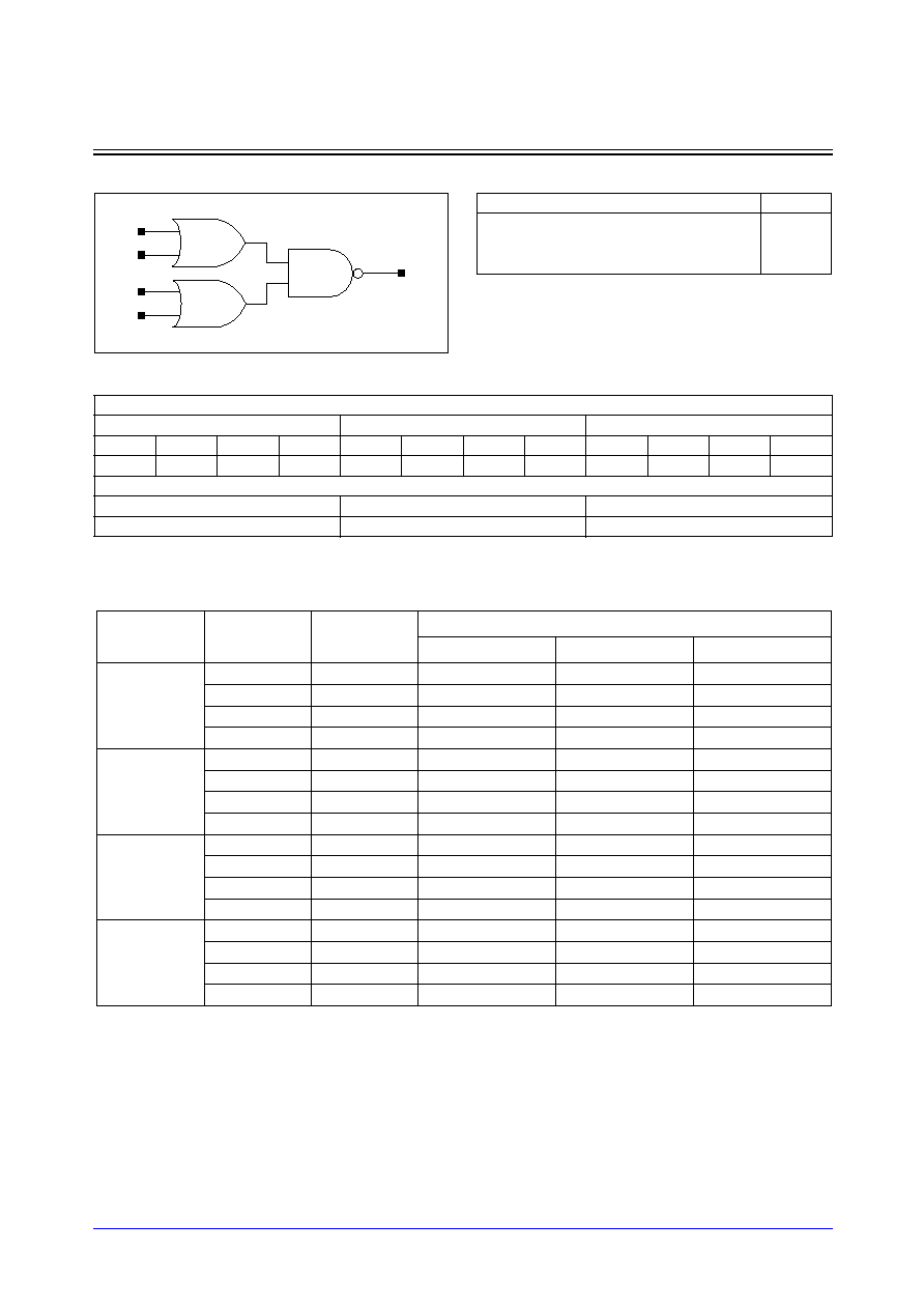
STDL131
3-130
Samsung ASIC
OA22_LP/OA22D2_LP/OA22D4_LP
Two 2-ORs into 2-NAND with 1X/2X/4X Drive
Logic Symbol
Cell Data
Switching Characteristics
(Typical process, 25
∞
C, 1.8V, t
R
/t
F
= 0.19ns, SL: Standard Load)
OA22_LP
Input Load (SL)
OA22_LP
OA22D2_LP
OA22D4_LP
A
B
C
D
A
B
C
D
A
B
C
D
1.1
1.1
1.1
1.1
2.0
2.1
2.0
2.2
0.9
0.9
1.0
1.0
Gate Count
OA22_LP
OA22D2_LP
OA22D4_LP
1.67
3.00
3.33
C
D
Y
A
B
Path
Parameter
Delay [ns]
SL = 2
Delay Equations [ns]
Group1*
Group2*
Group3*
A to Y
tR
0.296
0.196 + 0.050*SL
0.185 + 0.053*SL
0.174 + 0.054*SL
tF
0.163
0.101 + 0.031*SL
0.095 + 0.032*SL
0.088 + 0.033*SL
tPLH
0.152
0.099 + 0.027*SL
0.100 + 0.026*SL
0.100 + 0.026*SL
tPHL
0.139
0.102 + 0.018*SL
0.104 + 0.018*SL
0.106 + 0.018*SL
B to Y
tR
0.288
0.184 + 0.052*SL
0.179 + 0.053*SL
0.173 + 0.054*SL
tF
0.186
0.123 + 0.032*SL
0.119 + 0.032*SL
0.113 + 0.033*SL
tPLH
0.172
0.119 + 0.027*SL
0.119 + 0.026*SL
0.120 + 0.026*SL
tPHL
0.157
0.120 + 0.019*SL
0.123 + 0.018*SL
0.125 + 0.018*SL
C to Y
tR
0.256
0.153 + 0.052*SL
0.146 + 0.053*SL
0.138 + 0.054*SL
tF
0.157
0.093 + 0.032*SL
0.090 + 0.033*SL
0.086 + 0.033*SL
tPLH
0.184
0.131 + 0.027*SL
0.132 + 0.027*SL
0.133 + 0.026*SL
tPHL
0.146
0.109 + 0.019*SL
0.111 + 0.018*SL
0.114 + 0.018*SL
D to Y
tR
0.251
0.144 + 0.053*SL
0.141 + 0.054*SL
0.139 + 0.054*SL
tF
0.181
0.116 + 0.032*SL
0.114 + 0.033*SL
0.111 + 0.033*SL
tPLH
0.204
0.150 + 0.027*SL
0.151 + 0.026*SL
0.152 + 0.026*SL
tPHL
0.165
0.128 + 0.019*SL
0.131 + 0.018*SL
0.133 + 0.018*SL
*Group1 : SL < 4, *Group2 : 4 SL
<
<
=
= 8, *Group3 : 8 < SL
Truth Table
A
B
C
D
Y
0
0
x
x
1
x
x
0
0
1
Other States
0

Samsung ASIC
3-131
STDL131
OA22_LP/OA22D2_LP/OA22D4_LP
Two 2-ORs into 2-NAND with 1X/2X/4X Drive
Switching Characteristics
(Typical process, 25
∞
C, 1.8V, t
R
/t
F
= 0.19ns, SL: Standard Load)
OA22D2_LP
OA22D4_LP
Path
Parameter
Delay [ns]
SL = 2
Delay Equations [ns]
Group1*
Group2*
Group3*
A to Y
tR
0.242
0.195 + 0.023*SL
0.187 + 0.025*SL
0.171 + 0.027*SL
tF
0.130
0.099 + 0.016*SL
0.098 + 0.016*SL
0.089 + 0.017*SL
tPLH
0.122
0.096 + 0.013*SL
0.096 + 0.013*SL
0.097 + 0.013*SL
tPHL
0.119
0.100 + 0.010*SL
0.101 + 0.009*SL
0.104 + 0.009*SL
B to Y
tR
0.231
0.181 + 0.025*SL
0.176 + 0.026*SL
0.169 + 0.027*SL
tF
0.152
0.120 + 0.016*SL
0.120 + 0.016*SL
0.113 + 0.016*SL
tPLH
0.142
0.115 + 0.014*SL
0.117 + 0.013*SL
0.117 + 0.013*SL
tPHL
0.137
0.118 + 0.010*SL
0.119 + 0.009*SL
0.123 + 0.009*SL
C to Y
tR
0.195
0.145 + 0.025*SL
0.140 + 0.026*SL
0.131 + 0.027*SL
tF
0.123
0.092 + 0.015*SL
0.088 + 0.016*SL
0.085 + 0.017*SL
tPLH
0.152
0.125 + 0.013*SL
0.125 + 0.013*SL
0.127 + 0.013*SL
tPHL
0.123
0.104 + 0.010*SL
0.106 + 0.009*SL
0.109 + 0.009*SL
D to Y
tR
0.188
0.135 + 0.026*SL
0.134 + 0.027*SL
0.130 + 0.027*SL
tF
0.146
0.113 + 0.016*SL
0.113 + 0.016*SL
0.110 + 0.017*SL
tPLH
0.172
0.145 + 0.013*SL
0.146 + 0.013*SL
0.147 + 0.013*SL
tPHL
0.143
0.124 + 0.010*SL
0.126 + 0.009*SL
0.130 + 0.009*SL
*Group1 : SL < 4, *Group2 : 4 SL
<
<
=
= 12, *Group3 : 12 < SL
Path
Parameter
Delay [ns]
SL = 2
Delay Equations [ns]
Group1*
Group2*
Group3*
A to Y
tR
0.070
0.059 + 0.006*SL
0.057 + 0.006*SL
0.047 + 0.006*SL
tF
0.055
0.045 + 0.005*SL
0.048 + 0.004*SL
0.049 + 0.004*SL
tPLH
0.320
0.309 + 0.005*SL
0.315 + 0.004*SL
0.325 + 0.003*SL
tPHL
0.268
0.258 + 0.005*SL
0.264 + 0.003*SL
0.278 + 0.003*SL
B to Y
tR
0.070
0.059 + 0.006*SL
0.059 + 0.006*SL
0.047 + 0.006*SL
tF
0.056
0.048 + 0.004*SL
0.048 + 0.004*SL
0.049 + 0.004*SL
tPLH
0.339
0.329 + 0.005*SL
0.335 + 0.004*SL
0.345 + 0.003*SL
tPHL
0.287
0.278 + 0.005*SL
0.284 + 0.003*SL
0.298 + 0.003*SL
C to Y
tR
0.070
0.057 + 0.006*SL
0.060 + 0.006*SL
0.049 + 0.006*SL
tF
0.056
0.046 + 0.005*SL
0.049 + 0.004*SL
0.049 + 0.004*SL
tPLH
0.349
0.338 + 0.005*SL
0.344 + 0.004*SL
0.354 + 0.003*SL
tPHL
0.273
0.264 + 0.005*SL
0.269 + 0.003*SL
0.283 + 0.003*SL
D to Y
tR
0.070
0.059 + 0.006*SL
0.058 + 0.006*SL
0.048 + 0.006*SL
tF
0.056
0.047 + 0.005*SL
0.050 + 0.004*SL
0.049 + 0.004*SL
tPLH
0.369
0.358 + 0.005*SL
0.364 + 0.004*SL
0.374 + 0.003*SL
tPHL
0.291
0.282 + 0.005*SL
0.288 + 0.003*SL
0.302 + 0.003*SL
*Group1 : SL < 4, *Group2 : 4 SL
<
<
=
= 20, *Group3 : 20 < SL

STDL131
3-132
Samsung ASIC
OA22A_LP/OA22D2A_LP/OA22D4A_LP
2-OR and 2-NAND into 2-NAND with 1X/2X/4X Drive
Logic Symbol
Cell Data
Switching Characteristics
(Typical process, 25
∞
C, 1.8V, t
R
/t
F
= 0.19ns, SL: Standard Load)
OA22A_LP
Input Load (SL)
OA22A_LP
OA22D2A_LP
OA22D4A_LP
A
B
C
D
A
B
C
D
A
B
C
D
1.1
1.1
0.9
1.0
2.2
2.1
0.9
1.0
1.1
1.1
0.9
1.0
Gate Count
OA22A_LP
OA22D2A_LP
OA22D4A_LP
2.00
3.00
4.00
C
D
Y
A
B
Path
Parameter
Delay [ns]
SL = 2
Delay Equations [ns]
Group1*
Group2*
Group3*
A to Y
tR
0.221
0.119 + 0.051*SL
0.111 + 0.053*SL
0.100 + 0.054*SL
tF
0.137
0.081 + 0.028*SL
0.072 + 0.030*SL
0.064 + 0.031*SL
tPLH
0.150
0.097 + 0.027*SL
0.097 + 0.026*SL
0.098 + 0.026*SL
tPHL
0.110
0.074 + 0.018*SL
0.079 + 0.017*SL
0.079 + 0.017*SL
B to Y
tR
0.213
0.107 + 0.053*SL
0.103 + 0.054*SL
0.099 + 0.054*SL
tF
0.160
0.101 + 0.029*SL
0.097 + 0.031*SL
0.088 + 0.032*SL
tPLH
0.170
0.116 + 0.027*SL
0.117 + 0.026*SL
0.118 + 0.026*SL
tPHL
0.130
0.095 + 0.018*SL
0.097 + 0.017*SL
0.098 + 0.017*SL
C to Y
tR
0.122
0.071 + 0.025*SL
0.069 + 0.026*SL
0.066 + 0.026*SL
tF
0.147
0.084 + 0.031*SL
0.082 + 0.032*SL
0.080 + 0.032*SL
tPLH
0.178
0.152 + 0.013*SL
0.154 + 0.013*SL
0.155 + 0.012*SL
tPHL
0.216
0.180 + 0.018*SL
0.183 + 0.017*SL
0.185 + 0.017*SL
D to Y
tR
0.122
0.071 + 0.025*SL
0.069 + 0.026*SL
0.066 + 0.026*SL
tF
0.147
0.084 + 0.031*SL
0.081 + 0.032*SL
0.081 + 0.032*SL
tPLH
0.175
0.148 + 0.013*SL
0.151 + 0.013*SL
0.152 + 0.012*SL
tPHL
0.224
0.188 + 0.018*SL
0.191 + 0.017*SL
0.194 + 0.017*SL
*Group1 : SL < 4, *Group2 : 4 SL
<
<
=
= 8, *Group3 : 8 < SL
Truth Table
A
B
C
D
Y
0
0
x
x
1
x
x
1
1
1
Other States
0
Samsung ASIC
3-133
STDL131
OA22A_LP/OA22D2A_LP/OA22D4A_LP
2-OR and 2-NAND into 2-NAND with 1X/2X/4X Drive
Switching Characteristics
(Typical process, 25
∞
C, 1.8V, t
R
/t
F
= 0.19ns, SL: Standard Load)
OA22D2A_LP
OA22D4A_LP
Path
Parameter
Delay [ns]
SL = 2
Delay Equations [ns]
Group1*
Group2*
Group3*
A to Y
tR
0.169
0.121 + 0.024*SL
0.115 + 0.026*SL
0.100 + 0.027*SL
tF
0.109
0.082 + 0.014*SL
0.078 + 0.015*SL
0.067 + 0.016*SL
tPLH
0.122
0.096 + 0.013*SL
0.096 + 0.013*SL
0.097 + 0.013*SL
tPHL
0.091
0.071 + 0.010*SL
0.077 + 0.009*SL
0.079 + 0.008*SL
B to Y
tR
0.158
0.107 + 0.025*SL
0.103 + 0.026*SL
0.098 + 0.027*SL
tF
0.131
0.104 + 0.014*SL
0.099 + 0.015*SL
0.090 + 0.016*SL
tPLH
0.141
0.115 + 0.013*SL
0.116 + 0.013*SL
0.117 + 0.013*SL
tPHL
0.111
0.093 + 0.009*SL
0.095 + 0.009*SL
0.097 + 0.009*SL
C to Y
tR
0.106
0.082 + 0.012*SL
0.079 + 0.013*SL
0.076 + 0.013*SL
tF
0.119
0.088 + 0.015*SL
0.086 + 0.016*SL
0.083 + 0.016*SL
tPLH
0.196
0.181 + 0.007*SL
0.184 + 0.007*SL
0.188 + 0.006*SL
tPHL
0.223
0.204 + 0.010*SL
0.207 + 0.009*SL
0.212 + 0.008*SL
D to Y
tR
0.106
0.080 + 0.013*SL
0.081 + 0.013*SL
0.075 + 0.013*SL
tF
0.119
0.088 + 0.016*SL
0.088 + 0.016*SL
0.084 + 0.016*SL
tPLH
0.192
0.177 + 0.008*SL
0.181 + 0.007*SL
0.185 + 0.006*SL
tPHL
0.232
0.213 + 0.010*SL
0.215 + 0.009*SL
0.219 + 0.009*SL
*Group1 : SL < 4, *Group2 : 4 SL
<
<
=
= 12, *Group3 : 12 < SL
Path
Parameter
Delay [ns]
SL = 2
Delay Equations [ns]
Group1*
Group2*
Group3*
A to Y
tR
0.064
0.053 + 0.005*SL
0.051 + 0.006*SL
0.043 + 0.006*SL
tF
0.056
0.047 + 0.004*SL
0.048 + 0.004*SL
0.050 + 0.004*SL
tPLH
0.281
0.271 + 0.005*SL
0.276 + 0.004*SL
0.284 + 0.003*SL
tPHL
0.249
0.240 + 0.005*SL
0.246 + 0.003*SL
0.259 + 0.003*SL
B to Y
tR
0.064
0.053 + 0.006*SL
0.051 + 0.006*SL
0.042 + 0.006*SL
tF
0.056
0.045 + 0.005*SL
0.051 + 0.004*SL
0.050 + 0.004*SL
tPLH
0.301
0.291 + 0.005*SL
0.296 + 0.004*SL
0.304 + 0.003*SL
tPHL
0.274
0.264 + 0.005*SL
0.270 + 0.003*SL
0.284 + 0.003*SL
C to Y
tR
0.064
0.053 + 0.006*SL
0.051 + 0.006*SL
0.041 + 0.006*SL
tF
0.057
0.047 + 0.005*SL
0.050 + 0.004*SL
0.050 + 0.004*SL
tPLH
0.310
0.300 + 0.005*SL
0.305 + 0.004*SL
0.313 + 0.003*SL
tPHL
0.359
0.350 + 0.005*SL
0.356 + 0.003*SL
0.370 + 0.003*SL
D to Y
tR
0.063
0.052 + 0.006*SL
0.051 + 0.006*SL
0.041 + 0.006*SL
tF
0.057
0.047 + 0.005*SL
0.050 + 0.004*SL
0.050 + 0.004*SL
tPLH
0.306
0.297 + 0.005*SL
0.302 + 0.004*SL
0.309 + 0.003*SL
tPHL
0.369
0.360 + 0.005*SL
0.366 + 0.003*SL
0.379 + 0.003*SL
*Group1 : SL < 4, *Group2 : 4 SL
<
<
=
= 20, *Group3 : 20 < SL
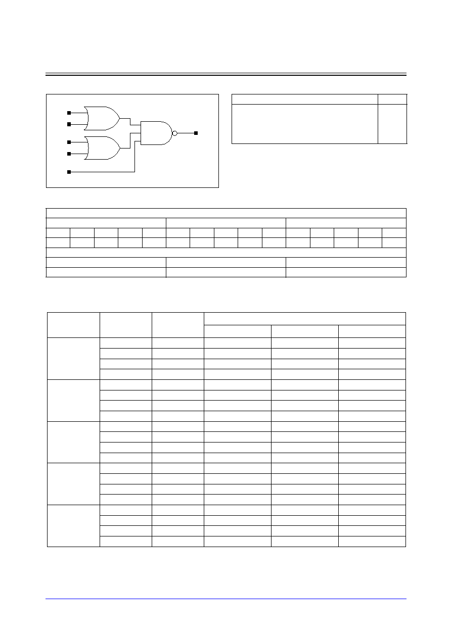
STDL131
3-134
Samsung ASIC
OA221_LP/OA221D2_LP/OA221D4_LP
Two 2-ORs into 3-NAND with 1X/2X/4X Drive
Logic Symbol
Cell Data
Switching Characteristics
(Typical process, 25
∞
C, 1.8V, t
R
/t
F
= 0.19ns, SL: Standard Load)
OA221_LP
Input Load (SL)
OA221_LP
OA221D2_LP
OA221D4_LP
A
B
C
D
E
A
B
C
D
E
A
B
C
D
E
1.1
1.1
1.1
1.2
1.0
2.1
2.2
2.3
2.3
2.2
0.9
0.9
0.9
1.0
1.0
Gate Count
OA221_LP
OA221D2_LP
OA221D4_LP
2.67
4.67
4.00
C
D
Y
A
B
E
Path
Parameter
Delay [ns]
SL = 2
Delay Equations [ns]
Group1*
Group2*
Group3*
A to Y
tR
0.331
0.232 + 0.050*SL
0.223 + 0.052*SL
0.213 + 0.053*SL
tF
0.233
0.153 + 0.040*SL
0.149 + 0.041*SL
0.143 + 0.042*SL
tPLH
0.172
0.120 + 0.026*SL
0.120 + 0.026*SL
0.121 + 0.026*SL
tPHL
0.175
0.130 + 0.023*SL
0.132 + 0.022*SL
0.134 + 0.022*SL
B to Y
tR
0.325
0.222 + 0.052*SL
0.217 + 0.053*SL
0.214 + 0.053*SL
tF
0.265
0.183 + 0.041*SL
0.180 + 0.042*SL
0.176 + 0.042*SL
tPLH
0.191
0.139 + 0.026*SL
0.139 + 0.026*SL
0.140 + 0.026*SL
tPHL
0.201
0.156 + 0.023*SL
0.158 + 0.022*SL
0.160 + 0.022*SL
C to Y
tR
0.293
0.190 + 0.052*SL
0.185 + 0.053*SL
0.179 + 0.054*SL
tF
0.231
0.150 + 0.041*SL
0.148 + 0.041*SL
0.143 + 0.042*SL
tPLH
0.204
0.151 + 0.026*SL
0.152 + 0.026*SL
0.153 + 0.026*SL
tPHL
0.190
0.145 + 0.023*SL
0.147 + 0.022*SL
0.150 + 0.022*SL
D to Y
tR
0.290
0.185 + 0.053*SL
0.181 + 0.053*SL
0.180 + 0.054*SL
tF
0.263
0.180 + 0.042*SL
0.179 + 0.042*SL
0.176 + 0.042*SL
tPLH
0.223
0.170 + 0.026*SL
0.171 + 0.026*SL
0.172 + 0.026*SL
tPHL
0.217
0.171 + 0.023*SL
0.173 + 0.022*SL
0.176 + 0.022*SL
E to Y
tR
0.201
0.139 + 0.031*SL
0.136 + 0.032*SL
0.129 + 0.033*SL
tF
0.261
0.178 + 0.042*SL
0.177 + 0.042*SL
0.175 + 0.042*SL
tPLH
0.165
0.133 + 0.016*SL
0.134 + 0.016*SL
0.135 + 0.016*SL
tPHL
0.220
0.174 + 0.023*SL
0.177 + 0.022*SL
0.180 + 0.022*SL
*Group1 : SL < 4, *Group2 : 4 SL
<
<
=
= 8, *Group3 : 8 < SL
Truth Table
A
B
C
D
E
Y
0
0
x
x
x
1
x
x
0
0
x
1
x
x
x
x
0
1
Other States
0

Samsung ASIC
3-135
STDL131
OA221_LP/OA221D2_LP/OA221D4_LP
Two 2-ORs into 3-NAND with 1X/2X/4X Drive
Switching Characteristics
(Typical process, 25
∞
C, 1.8V, t
R
/t
F
= 0.19ns, SL: Standard Load)
OA221D2_LP
Path
Parameter
Delay [ns]
SL = 2
Delay Equations [ns]
Group1*
Group2*
Group3*
A to Y
tR
0.278
0.230 + 0.024*SL
0.224 + 0.026*SL
0.212 + 0.027*SL
tF
0.189
0.150 + 0.020*SL
0.147 + 0.020*SL
0.140 + 0.021*SL
tPLH
0.143
0.116 + 0.013*SL
0.117 + 0.013*SL
0.118 + 0.013*SL
tPHL
0.150
0.127 + 0.011*SL
0.128 + 0.011*SL
0.131 + 0.011*SL
B to Y
tR
0.269
0.218 + 0.026*SL
0.216 + 0.026*SL
0.210 + 0.027*SL
tF
0.221
0.181 + 0.020*SL
0.178 + 0.021*SL
0.173 + 0.021*SL
tPLH
0.163
0.137 + 0.013*SL
0.137 + 0.013*SL
0.138 + 0.013*SL
tPHL
0.176
0.152 + 0.012*SL
0.154 + 0.011*SL
0.157 + 0.011*SL
C to Y
tR
0.237
0.186 + 0.025*SL
0.183 + 0.026*SL
0.175 + 0.027*SL
tF
0.187
0.146 + 0.020*SL
0.145 + 0.021*SL
0.140 + 0.021*SL
tPLH
0.174
0.148 + 0.013*SL
0.148 + 0.013*SL
0.150 + 0.013*SL
tPHL
0.165
0.142 + 0.012*SL
0.144 + 0.011*SL
0.147 + 0.011*SL
D to Y
tR
0.231
0.179 + 0.026*SL
0.178 + 0.027*SL
0.174 + 0.027*SL
tF
0.218
0.177 + 0.020*SL
0.176 + 0.021*SL
0.173 + 0.021*SL
tPLH
0.194
0.167 + 0.013*SL
0.168 + 0.013*SL
0.169 + 0.013*SL
tPHL
0.192
0.168 + 0.012*SL
0.170 + 0.011*SL
0.173 + 0.011*SL
E to Y
tR
0.166
0.136 + 0.015*SL
0.134 + 0.016*SL
0.126 + 0.016*SL
tF
0.216
0.175 + 0.021*SL
0.174 + 0.021*SL
0.172 + 0.021*SL
tPLH
0.146
0.130 + 0.008*SL
0.130 + 0.008*SL
0.132 + 0.008*SL
tPHL
0.194
0.170 + 0.012*SL
0.172 + 0.011*SL
0.176 + 0.011*SL
*Group1 : SL < 4, *Group2 : 4 SL
<
<
=
= 12, *Group3 : 12 < SL

STDL131
3-136
Samsung ASIC
OA221_LP/OA221D2_LP/OA221D4_LP
Two 2-ORs into 3-NAND with 1X/2X/4X Drive
Switching Characteristics
(Typical process, 25
∞
C, 1.8V, t
R
/t
F
= 0.19ns, SL: Standard Load)
OA221D4_LP
Path
Parameter
Delay [ns]
SL = 2
Delay Equations [ns]
Group1*
Group2*
Group3*
A to Y
tR
0.071
0.060 + 0.005*SL
0.059 + 0.006*SL
0.049 + 0.006*SL
tF
0.059
0.048 + 0.005*SL
0.053 + 0.004*SL
0.052 + 0.004*SL
tPLH
0.342
0.331 + 0.005*SL
0.337 + 0.004*SL
0.347 + 0.003*SL
tPHL
0.327
0.317 + 0.005*SL
0.323 + 0.003*SL
0.337 + 0.003*SL
B to Y
tR
0.072
0.060 + 0.006*SL
0.061 + 0.006*SL
0.049 + 0.006*SL
tF
0.060
0.050 + 0.005*SL
0.053 + 0.004*SL
0.051 + 0.004*SL
tPLH
0.361
0.350 + 0.005*SL
0.356 + 0.004*SL
0.366 + 0.003*SL
tPHL
0.355
0.345 + 0.005*SL
0.351 + 0.003*SL
0.366 + 0.003*SL
C to Y
tR
0.070
0.056 + 0.007*SL
0.061 + 0.006*SL
0.051 + 0.006*SL
tF
0.059
0.049 + 0.005*SL
0.053 + 0.004*SL
0.051 + 0.004*SL
tPLH
0.371
0.361 + 0.005*SL
0.367 + 0.004*SL
0.377 + 0.003*SL
tPHL
0.341
0.332 + 0.005*SL
0.338 + 0.003*SL
0.352 + 0.003*SL
D to Y
tR
0.072
0.061 + 0.006*SL
0.059 + 0.006*SL
0.050 + 0.006*SL
tF
0.059
0.051 + 0.004*SL
0.051 + 0.004*SL
0.052 + 0.004*SL
tPLH
0.390
0.380 + 0.005*SL
0.386 + 0.004*SL
0.396 + 0.003*SL
tPHL
0.370
0.360 + 0.005*SL
0.367 + 0.003*SL
0.381 + 0.003*SL
E to Y
tR
0.068
0.056 + 0.006*SL
0.056 + 0.006*SL
0.044 + 0.006*SL
tF
0.059
0.049 + 0.005*SL
0.053 + 0.004*SL
0.053 + 0.004*SL
tPLH
0.295
0.286 + 0.005*SL
0.291 + 0.004*SL
0.300 + 0.003*SL
tPHL
0.378
0.368 + 0.005*SL
0.375 + 0.003*SL
0.389 + 0.003*SL
*Group1 : SL < 4, *Group2 : 4 SL
<
<
=
= 20, *Group3 : 20 < SL
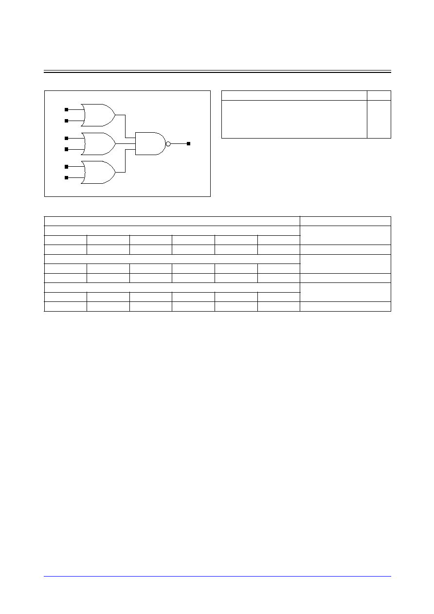
Samsung ASIC
3-137
STDL131
OA222_LP/OA222D2_LP/OA222D4_LP
Three 2-ORs into 3-NAND with 1X/2X/4X Drive
Logic Symbol
Cell Data
Input Load (SL)
Gate Count
OA222_LP
OA222_LP
A
B
C
D
E
F
1.1
1.1
1.1
1.1
1.1
1.2
2.67
OA222D2_LP
OA222D2_LP
A
B
C
D
E
F
2.1
2.2
2.1
2.2
2.1
2.2
4.67
OA222D4_LP
OA222D4_LP
A
B
C
D
E
F
0.9
0.9
0.9
0.9
0.9
1.0
4.67
C
D
Y
A
B
E
F
Truth Table
A
B
C
D
E
F
Y
0
0
x
x
x
x
1
x
x
0
0
x
x
1
x
x
x
x
0
0
1
Other States
0

STDL131
3-138
Samsung ASIC
OA222_LP/OA222D2_LP/OA222D4_LP
Three 2-ORs into 3-NAND with 1X/2X/4X Drive
Switching Characteristics
(Typical process, 25
∞
C, 1.8V, t
R
/t
F
= 0.19ns, SL: Standard Load)
OA222_LP
Path
Parameter
Delay [ns]
SL = 2
Delay Equations [ns]
Group1*
Group2*
Group3*
A to Y
tR
0.405
0.305 + 0.050*SL
0.296 + 0.052*SL
0.287 + 0.053*SL
tF
0.281
0.193 + 0.044*SL
0.190 + 0.045*SL
0.188 + 0.045*SL
tPLH
0.171
0.119 + 0.026*SL
0.119 + 0.026*SL
0.119 + 0.026*SL
tPHL
0.217
0.168 + 0.024*SL
0.170 + 0.024*SL
0.173 + 0.023*SL
B to Y
tR
0.398
0.295 + 0.052*SL
0.290 + 0.053*SL
0.287 + 0.053*SL
tF
0.313
0.225 + 0.044*SL
0.222 + 0.045*SL
0.221 + 0.045*SL
tPLH
0.190
0.138 + 0.026*SL
0.138 + 0.026*SL
0.139 + 0.026*SL
tPHL
0.244
0.195 + 0.024*SL
0.198 + 0.024*SL
0.201 + 0.023*SL
C to Y
tR
0.364
0.263 + 0.051*SL
0.256 + 0.053*SL
0.250 + 0.053*SL
tF
0.279
0.191 + 0.044*SL
0.188 + 0.045*SL
0.188 + 0.045*SL
tPLH
0.203
0.151 + 0.026*SL
0.151 + 0.026*SL
0.153 + 0.026*SL
tPHL
0.235
0.186 + 0.025*SL
0.188 + 0.024*SL
0.192 + 0.023*SL
D to Y
tR
0.361
0.257 + 0.052*SL
0.253 + 0.053*SL
0.250 + 0.053*SL
tF
0.313
0.224 + 0.044*SL
0.222 + 0.045*SL
0.222 + 0.045*SL
tPLH
0.225
0.173 + 0.026*SL
0.173 + 0.026*SL
0.174 + 0.026*SL
tPHL
0.264
0.216 + 0.024*SL
0.218 + 0.024*SL
0.221 + 0.023*SL
E to Y
tR
0.321
0.217 + 0.052*SL
0.213 + 0.053*SL
0.210 + 0.053*SL
tF
0.278
0.189 + 0.044*SL
0.187 + 0.045*SL
0.187 + 0.045*SL
tPLH
0.229
0.175 + 0.027*SL
0.177 + 0.026*SL
0.179 + 0.026*SL
tPHL
0.244
0.195 + 0.024*SL
0.198 + 0.024*SL
0.201 + 0.023*SL
F to Y
tR
0.319
0.213 + 0.053*SL
0.211 + 0.053*SL
0.210 + 0.053*SL
tF
0.312
0.223 + 0.045*SL
0.222 + 0.045*SL
0.222 + 0.045*SL
tPLH
0.250
0.196 + 0.027*SL
0.198 + 0.026*SL
0.200 + 0.026*SL
tPHL
0.273
0.224 + 0.024*SL
0.227 + 0.024*SL
0.230 + 0.023*SL
*Group1 : SL < 4, *Group2 : 4 SL
<
<
=
= 8, *Group3 : 8 < SL

Samsung ASIC
3-139
STDL131
OA222_LP/OA222D2_LP/OA222D4_LP
Three 2-ORs into 3-NAND with 1X/2X/4X Drive
Switching Characteristics
(Typical process, 25
∞
C, 1.8V, t
R
/t
F
= 0.19ns, SL: Standard Load)
OA222D2_LP
Path
Parameter
Delay [ns]
SL = 2
Delay Equations [ns]
Group1*
Group2*
Group3*
A to Y
tR
0.335
0.287 + 0.024*SL
0.281 + 0.025*SL
0.269 + 0.026*SL
tF
0.227
0.182 + 0.022*SL
0.181 + 0.022*SL
0.177 + 0.023*SL
tPLH
0.141
0.114 + 0.013*SL
0.115 + 0.013*SL
0.115 + 0.013*SL
tPHL
0.186
0.161 + 0.013*SL
0.162 + 0.012*SL
0.166 + 0.012*SL
B to Y
tR
0.327
0.276 + 0.026*SL
0.274 + 0.026*SL
0.267 + 0.027*SL
tF
0.256
0.212 + 0.022*SL
0.212 + 0.022*SL
0.209 + 0.023*SL
tPLH
0.159
0.133 + 0.013*SL
0.133 + 0.013*SL
0.134 + 0.013*SL
tPHL
0.211
0.186 + 0.012*SL
0.188 + 0.012*SL
0.191 + 0.012*SL
C to Y
tR
0.299
0.249 + 0.025*SL
0.245 + 0.026*SL
0.236 + 0.027*SL
tF
0.226
0.182 + 0.022*SL
0.181 + 0.022*SL
0.178 + 0.023*SL
tPLH
0.172
0.145 + 0.013*SL
0.146 + 0.013*SL
0.147 + 0.013*SL
tPHL
0.202
0.177 + 0.013*SL
0.179 + 0.012*SL
0.183 + 0.012*SL
D to Y
tR
0.293
0.241 + 0.026*SL
0.239 + 0.026*SL
0.235 + 0.027*SL
tF
0.256
0.211 + 0.022*SL
0.211 + 0.022*SL
0.209 + 0.023*SL
tPLH
0.190
0.164 + 0.013*SL
0.165 + 0.013*SL
0.166 + 0.013*SL
tPHL
0.229
0.204 + 0.012*SL
0.205 + 0.012*SL
0.209 + 0.012*SL
E to Y
tR
0.259
0.208 + 0.026*SL
0.205 + 0.026*SL
0.199 + 0.027*SL
tF
0.223
0.178 + 0.022*SL
0.178 + 0.022*SL
0.176 + 0.023*SL
tPLH
0.197
0.169 + 0.014*SL
0.171 + 0.013*SL
0.173 + 0.013*SL
tPHL
0.210
0.185 + 0.013*SL
0.187 + 0.012*SL
0.191 + 0.012*SL
F to Y
tR
0.255
0.202 + 0.026*SL
0.202 + 0.026*SL
0.199 + 0.027*SL
tF
0.255
0.210 + 0.022*SL
0.209 + 0.022*SL
0.209 + 0.023*SL
tPLH
0.216
0.189 + 0.014*SL
0.190 + 0.013*SL
0.192 + 0.013*SL
tPHL
0.238
0.213 + 0.012*SL
0.215 + 0.012*SL
0.218 + 0.012*SL
*Group1 : SL < 4, *Group2 : 4 SL
<
<
=
= 12, *Group3 : 12 < SL
STDL131
3-140
Samsung ASIC
OA222_LP/OA222D2_LP/OA222D4_LP
Three 2-ORs into 3-NAND with 1X/2X/4X Drive
Switching Characteristics
(Typical process, 25
∞
C, 1.8V, t
R
/t
F
= 0.19ns, SL: Standard Load)
OA222D4_LP
Path
Parameter
Delay [ns]
SL = 2
Delay Equations [ns]
Group1*
Group2*
Group3*
A to Y
tR
0.076
0.065 + 0.005*SL
0.063 + 0.006*SL
0.053 + 0.006*SL
tF
0.059
0.049 + 0.005*SL
0.053 + 0.004*SL
0.053 + 0.004*SL
tPLH
0.363
0.352 + 0.005*SL
0.359 + 0.004*SL
0.370 + 0.003*SL
tPHL
0.365
0.355 + 0.005*SL
0.361 + 0.003*SL
0.376 + 0.003*SL
B to Y
tR
0.075
0.061 + 0.007*SL
0.066 + 0.006*SL
0.054 + 0.006*SL
tF
0.059
0.049 + 0.005*SL
0.054 + 0.004*SL
0.053 + 0.004*SL
tPLH
0.381
0.371 + 0.005*SL
0.378 + 0.004*SL
0.389 + 0.003*SL
tPHL
0.390
0.380 + 0.005*SL
0.386 + 0.003*SL
0.401 + 0.003*SL
C to Y
tR
0.077
0.065 + 0.006*SL
0.066 + 0.006*SL
0.053 + 0.006*SL
tF
0.059
0.051 + 0.004*SL
0.051 + 0.004*SL
0.052 + 0.004*SL
tPLH
0.399
0.388 + 0.005*SL
0.395 + 0.004*SL
0.406 + 0.003*SL
tPHL
0.383
0.374 + 0.005*SL
0.380 + 0.003*SL
0.395 + 0.003*SL
D to Y
tR
0.076
0.064 + 0.006*SL
0.066 + 0.006*SL
0.055 + 0.006*SL
tF
0.060
0.049 + 0.005*SL
0.054 + 0.004*SL
0.053 + 0.004*SL
tPLH
0.418
0.407 + 0.005*SL
0.414 + 0.004*SL
0.426 + 0.003*SL
tPHL
0.410
0.400 + 0.005*SL
0.406 + 0.003*SL
0.421 + 0.003*SL
E to Y
tR
0.078
0.067 + 0.005*SL
0.065 + 0.006*SL
0.055 + 0.006*SL
tF
0.060
0.050 + 0.005*SL
0.053 + 0.004*SL
0.053 + 0.004*SL
tPLH
0.427
0.416 + 0.005*SL
0.423 + 0.004*SL
0.435 + 0.003*SL
tPHL
0.394
0.384 + 0.005*SL
0.390 + 0.003*SL
0.405 + 0.003*SL
F to Y
tR
0.077
0.066 + 0.006*SL
0.067 + 0.006*SL
0.054 + 0.006*SL
tF
0.060
0.049 + 0.005*SL
0.054 + 0.004*SL
0.053 + 0.004*SL
tPLH
0.447
0.436 + 0.005*SL
0.443 + 0.004*SL
0.454 + 0.003*SL
tPHL
0.418
0.408 + 0.005*SL
0.415 + 0.003*SL
0.429 + 0.003*SL
*Group1 : SL < 4, *Group2 : 4 SL
<
<
=
= 20, *Group3 : 20 < SL
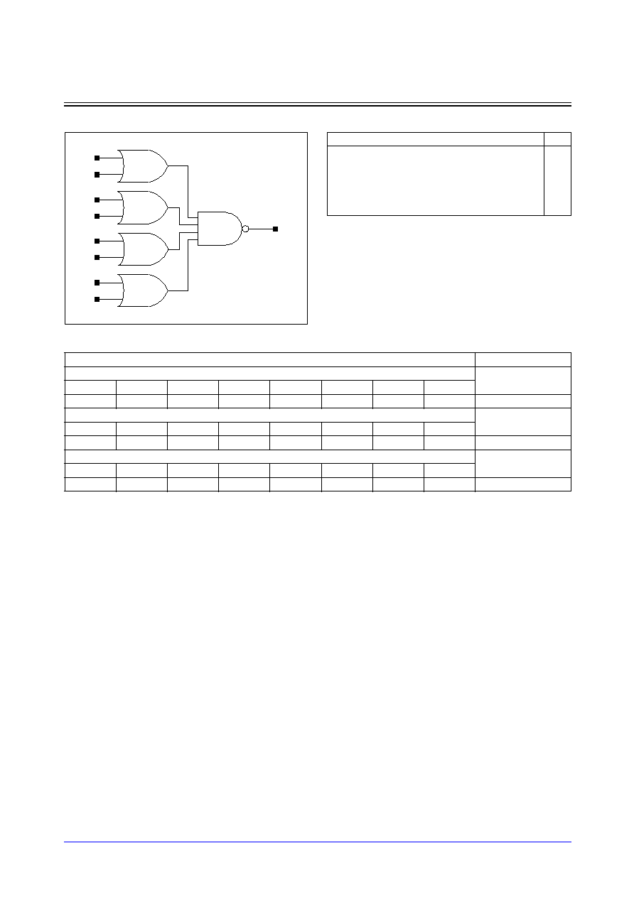
Samsung ASIC
3-141
STDL131
OA2222_LP/OA2222D2_LP/OA2222D4_LP
Four 2-ORs into 4-NAND with 1X/2X/4X Drive
Logic Symbol
Cell Data
Input Load (SL)
Gate Count
OA2222_LP
OA2222_LP
A
B
C
D
E
F
G
H
1.1
1.1
1.1
1.1
1.1
1.1
1.1
1.1
3.67
OA2222D2_LP
OA2222D2_LP
A
B
C
D
E
F
G
H
0.9
0.9
0.9
0.9
0.9
0.9
1.0
1.0
4.33
OA2222D4_LP
OA2222D4_LP
A
B
C
D
E
F
G
H
0.9
0.9
0.9
0.9
0.9
1.0
1.0
1.0
5.00
E
F
Y
C
D
G
H
A
B
Truth Table
A
B
C
D
E
F
G
H
Y
0
0
x
x
x
x
x
x
1
x
x
0
0
x
x
x
x
1
x
x
x
x
0
0
x
x
1
x
x
x
x
x
x
0
0
1
Other States
0

STDL131
3-142
Samsung ASIC
OA2222_LP/OA2222D2_LP/OA2222D4_LP
Four 2-ORs into 4-NAND with 1X/2X/4X Drive
Switching Characteristics
(Typical process, 25
∞
C, 1.8V, t
R
/t
F
= 0.19ns, SL: Standard Load)
OA2222_LP
Path
Parameter
Delay [ns]
SL = 2
Delay Equations [ns]
Group1*
Group2*
Group3*
A to Y
tR
0.493
0.391 + 0.051*SL
0.383 + 0.053*SL
0.375 + 0.054*SL
tF
0.340
0.239 + 0.051*SL
0.236 + 0.051*SL
0.236 + 0.051*SL
tPLH
0.185
0.132 + 0.027*SL
0.133 + 0.026*SL
0.133 + 0.026*SL
tPHL
0.247
0.193 + 0.027*SL
0.195 + 0.027*SL
0.198 + 0.026*SL
B to Y
tR
0.488
0.382 + 0.053*SL
0.378 + 0.054*SL
0.376 + 0.054*SL
tF
0.377
0.276 + 0.051*SL
0.274 + 0.051*SL
0.274 + 0.051*SL
tPLH
0.205
0.152 + 0.026*SL
0.152 + 0.026*SL
0.153 + 0.026*SL
tPHL
0.278
0.223 + 0.027*SL
0.226 + 0.027*SL
0.228 + 0.026*SL
C to Y
tR
0.460
0.356 + 0.052*SL
0.350 + 0.054*SL
0.345 + 0.054*SL
tF
0.340
0.239 + 0.051*SL
0.238 + 0.051*SL
0.238 + 0.051*SL
tPLH
0.220
0.167 + 0.027*SL
0.167 + 0.027*SL
0.169 + 0.026*SL
tPHL
0.272
0.218 + 0.027*SL
0.220 + 0.027*SL
0.223 + 0.026*SL
D to Y
tR
0.457
0.351 + 0.053*SL
0.347 + 0.054*SL
0.345 + 0.054*SL
tF
0.378
0.276 + 0.051*SL
0.276 + 0.051*SL
0.275 + 0.051*SL
tPLH
0.240
0.187 + 0.027*SL
0.187 + 0.026*SL
0.188 + 0.026*SL
tPHL
0.304
0.249 + 0.027*SL
0.252 + 0.027*SL
0.255 + 0.026*SL
E to Y
tR
0.478
0.376 + 0.051*SL
0.370 + 0.053*SL
0.366 + 0.053*SL
tF
0.341
0.239 + 0.051*SL
0.239 + 0.051*SL
0.239 + 0.051*SL
tPLH
0.246
0.192 + 0.027*SL
0.194 + 0.026*SL
0.196 + 0.026*SL
tPHL
0.287
0.232 + 0.027*SL
0.235 + 0.027*SL
0.238 + 0.026*SL
F to Y
tR
0.476
0.372 + 0.052*SL
0.369 + 0.053*SL
0.366 + 0.053*SL
tF
0.377
0.276 + 0.051*SL
0.276 + 0.051*SL
0.275 + 0.051*SL
tPLH
0.264
0.211 + 0.027*SL
0.213 + 0.026*SL
0.214 + 0.026*SL
tPHL
0.318
0.264 + 0.027*SL
0.266 + 0.027*SL
0.269 + 0.026*SL
G to Y
tR
0.584
0.479 + 0.052*SL
0.474 + 0.054*SL
0.470 + 0.054*SL
tF
0.433
0.318 + 0.058*SL
0.317 + 0.058*SL
0.317 + 0.058*SL
tPLH
0.273
0.218 + 0.028*SL
0.221 + 0.027*SL
0.224 + 0.027*SL
tPHL
0.376
0.314 + 0.031*SL
0.317 + 0.030*SL
0.321 + 0.030*SL
H to Y
tR
0.583
0.477 + 0.053*SL
0.474 + 0.054*SL
0.471 + 0.054*SL
tF
0.473
0.357 + 0.058*SL
0.357 + 0.058*SL
0.358 + 0.058*SL
tPLH
0.293
0.238 + 0.028*SL
0.240 + 0.027*SL
0.243 + 0.027*SL
tPHL
0.410
0.348 + 0.031*SL
0.351 + 0.030*SL
0.354 + 0.030*SL
*Group1 : SL < 4, *Group2 : 4 SL
<
<
=
= 8, *Group3 : 8 < SL

Samsung ASIC
3-143
STDL131
OA2222_LP/OA2222D2_LP/OA2222D4_LP
Four 2-ORs into 4-NAND with 1X/2X/4X Drive
Switching Characteristics
(Typical process, 25
∞
C, 1.8V, t
R
/t
F
= 0.19ns, SL: Standard Load)
OA2222D2_LP
Path
Parameter
Delay [ns]
SL = 2
Delay Equations [ns]
Group1*
Group2*
Group3*
A to Y
tR
0.082
0.060 + 0.011*SL
0.055 + 0.012*SL
0.045 + 0.013*SL
tF
0.058
0.042 + 0.008*SL
0.041 + 0.008*SL
0.038 + 0.008*SL
tPLH
0.354
0.337 + 0.009*SL
0.345 + 0.007*SL
0.350 + 0.006*SL
tPHL
0.365
0.351 + 0.007*SL
0.358 + 0.006*SL
0.365 + 0.005*SL
B to Y
tR
0.082
0.061 + 0.011*SL
0.056 + 0.012*SL
0.043 + 0.013*SL
tF
0.057
0.041 + 0.008*SL
0.042 + 0.008*SL
0.037 + 0.008*SL
tPLH
0.373
0.355 + 0.009*SL
0.363 + 0.007*SL
0.368 + 0.006*SL
tPHL
0.394
0.380 + 0.007*SL
0.387 + 0.006*SL
0.395 + 0.005*SL
C to Y
tR
0.083
0.062 + 0.011*SL
0.056 + 0.012*SL
0.045 + 0.013*SL
tF
0.057
0.041 + 0.008*SL
0.042 + 0.008*SL
0.037 + 0.008*SL
tPLH
0.390
0.373 + 0.009*SL
0.381 + 0.007*SL
0.386 + 0.006*SL
tPHL
0.389
0.375 + 0.007*SL
0.381 + 0.006*SL
0.389 + 0.005*SL
D to Y
tR
0.083
0.062 + 0.011*SL
0.057 + 0.012*SL
0.043 + 0.013*SL
tF
0.058
0.041 + 0.009*SL
0.044 + 0.008*SL
0.039 + 0.008*SL
tPLH
0.411
0.394 + 0.009*SL
0.402 + 0.007*SL
0.406 + 0.006*SL
tPHL
0.421
0.406 + 0.007*SL
0.413 + 0.006*SL
0.421 + 0.005*SL
E to Y
tR
0.083
0.059 + 0.012*SL
0.059 + 0.012*SL
0.047 + 0.013*SL
tF
0.058
0.041 + 0.008*SL
0.043 + 0.008*SL
0.038 + 0.008*SL
tPLH
0.419
0.401 + 0.009*SL
0.410 + 0.007*SL
0.415 + 0.006*SL
tPHL
0.405
0.391 + 0.007*SL
0.397 + 0.006*SL
0.405 + 0.005*SL
F to Y
tR
0.084
0.063 + 0.011*SL
0.058 + 0.012*SL
0.046 + 0.013*SL
tF
0.059
0.042 + 0.008*SL
0.043 + 0.008*SL
0.039 + 0.008*SL
tPLH
0.438
0.420 + 0.009*SL
0.428 + 0.007*SL
0.434 + 0.006*SL
tPHL
0.435
0.420 + 0.007*SL
0.427 + 0.006*SL
0.435 + 0.005*SL
G to Y
tR
0.085
0.062 + 0.011*SL
0.061 + 0.012*SL
0.046 + 0.013*SL
tF
0.060
0.044 + 0.008*SL
0.045 + 0.008*SL
0.039 + 0.008*SL
tPLH
0.442
0.424 + 0.009*SL
0.433 + 0.007*SL
0.438 + 0.006*SL
tPHL
0.490
0.476 + 0.007*SL
0.483 + 0.006*SL
0.491 + 0.005*SL
H to Y
tR
0.085
0.064 + 0.011*SL
0.058 + 0.012*SL
0.048 + 0.013*SL
tF
0.060
0.043 + 0.008*SL
0.045 + 0.008*SL
0.040 + 0.008*SL
tPLH
0.461
0.443 + 0.009*SL
0.452 + 0.007*SL
0.457 + 0.006*SL
tPHL
0.524
0.509 + 0.007*SL
0.516 + 0.006*SL
0.525 + 0.005*SL
*Group1 : SL < 4, *Group2 : 4 SL
<
<
=
= 12, *Group3 : 12 < SL

STDL131
3-144
Samsung ASIC
OA2222_LP/OA2222D2_LP/OA2222D4_LP
Four 2-ORs into 4-NAND with 1X/2X/4X Drive
Switching Characteristics
(Typical process, 25
∞
C, 1.8V, t
R
/t
F
= 0.19ns, SL: Standard Load)
OA2222D4_LP
Path
Parameter
Delay [ns]
SL = 2
Delay Equations [ns]
Group1*
Group2*
Group3*
A to Y
tR
0.081
0.070 + 0.005*SL
0.068 + 0.006*SL
0.058 + 0.006*SL
tF
0.061
0.052 + 0.005*SL
0.055 + 0.004*SL
0.055 + 0.004*SL
tPLH
0.389
0.377 + 0.006*SL
0.385 + 0.004*SL
0.397 + 0.003*SL
tPHL
0.404
0.394 + 0.005*SL
0.401 + 0.003*SL
0.416 + 0.003*SL
B to Y
tR
0.079
0.065 + 0.007*SL
0.070 + 0.006*SL
0.057 + 0.006*SL
tF
0.062
0.052 + 0.005*SL
0.056 + 0.004*SL
0.054 + 0.004*SL
tPLH
0.407
0.395 + 0.006*SL
0.403 + 0.004*SL
0.415 + 0.003*SL
tPHL
0.434
0.424 + 0.005*SL
0.430 + 0.003*SL
0.445 + 0.003*SL
C to Y
tR
0.081
0.069 + 0.006*SL
0.069 + 0.006*SL
0.058 + 0.006*SL
tF
0.061
0.051 + 0.005*SL
0.056 + 0.004*SL
0.055 + 0.004*SL
tPLH
0.424
0.413 + 0.006*SL
0.421 + 0.004*SL
0.433 + 0.003*SL
tPHL
0.427
0.417 + 0.005*SL
0.424 + 0.003*SL
0.439 + 0.003*SL
D to Y
tR
0.080
0.067 + 0.007*SL
0.070 + 0.006*SL
0.058 + 0.006*SL
tF
0.062
0.053 + 0.005*SL
0.055 + 0.004*SL
0.055 + 0.004*SL
tPLH
0.445
0.434 + 0.006*SL
0.442 + 0.004*SL
0.454 + 0.003*SL
tPHL
0.460
0.450 + 0.005*SL
0.456 + 0.003*SL
0.472 + 0.003*SL
E to Y
tR
0.081
0.068 + 0.007*SL
0.072 + 0.006*SL
0.059 + 0.006*SL
tF
0.062
0.052 + 0.005*SL
0.055 + 0.004*SL
0.054 + 0.004*SL
tPLH
0.454
0.443 + 0.006*SL
0.450 + 0.004*SL
0.463 + 0.003*SL
tPHL
0.444
0.434 + 0.005*SL
0.440 + 0.003*SL
0.456 + 0.003*SL
F to Y
tR
0.082
0.071 + 0.006*SL
0.071 + 0.006*SL
0.059 + 0.006*SL
tF
0.062
0.052 + 0.005*SL
0.055 + 0.004*SL
0.055 + 0.004*SL
tPLH
0.473
0.462 + 0.006*SL
0.469 + 0.004*SL
0.482 + 0.003*SL
tPHL
0.474
0.464 + 0.005*SL
0.470 + 0.003*SL
0.486 + 0.003*SL
G to Y
tR
0.081
0.066 + 0.007*SL
0.073 + 0.006*SL
0.060 + 0.006*SL
tF
0.064
0.055 + 0.005*SL
0.057 + 0.004*SL
0.057 + 0.004*SL
tPLH
0.478
0.466 + 0.006*SL
0.474 + 0.004*SL
0.488 + 0.003*SL
tPHL
0.532
0.522 + 0.005*SL
0.528 + 0.003*SL
0.544 + 0.003*SL
H to Y
tR
0.083
0.072 + 0.006*SL
0.071 + 0.006*SL
0.061 + 0.006*SL
tF
0.064
0.054 + 0.005*SL
0.058 + 0.004*SL
0.057 + 0.004*SL
tPLH
0.497
0.486 + 0.006*SL
0.493 + 0.004*SL
0.507 + 0.003*SL
tPHL
0.566
0.556 + 0.005*SL
0.562 + 0.003*SL
0.578 + 0.003*SL
*Group1 : SL < 4, *Group2 : 4 SL
<
<
=
= 20, *Group3 : 20 < SL
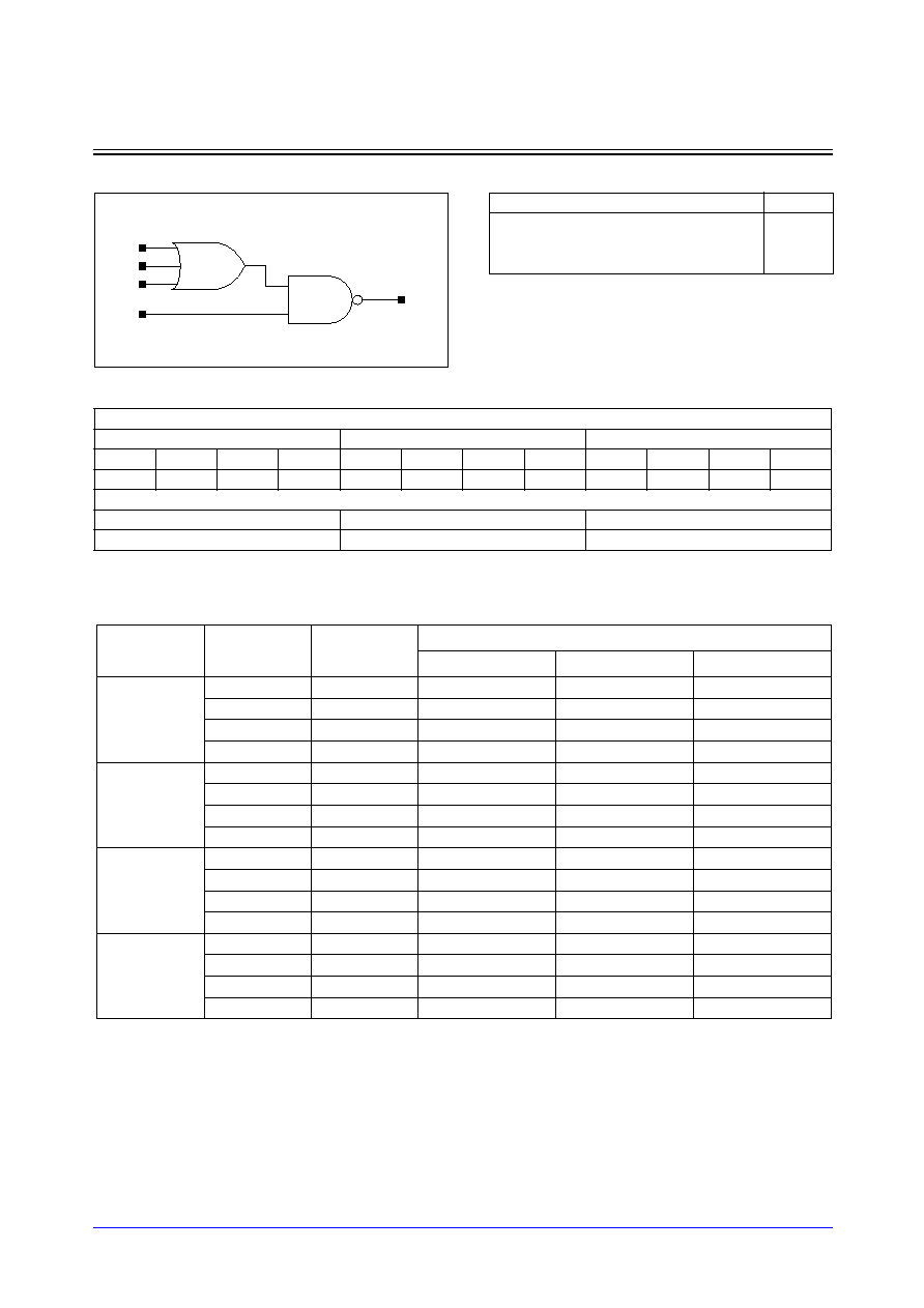
Samsung ASIC
3-145
STDL131
OA31_LP/OA31D2_LP/OA31D4_LP
3-OR into 2-NAND with 1X/2X/4X Drive
Logic Symbol
Cell Data
Switching Characteristics
(Typical process, 25
∞
C, 1.8V, t
R
/t
F
= 0.19ns, SL: Standard Load)
OA31_LP
Input Load (SL)
OA31_LP
OA31D2_LP
OA31D4_LP
A
B
C
D
A
B
C
D
A
B
C
D
1.0
1.0
1.0
0.7
1.9
2.0
2.0
1.3
0.9
0.9
0.9
0.9
Gate Count
OA31_LP
OA31D2_LP
OA31D4_LP
1.67
3.00
3.33
C
D
Y
A
B
Path
Parameter
Delay [ns]
SL = 2
Delay Equations [ns]
Group1*
Group2*
Group3*
A to Y
tR
0.343
0.188 + 0.077*SL
0.177 + 0.080*SL
0.176 + 0.080*SL
tF
0.190
0.101 + 0.045*SL
0.093 + 0.047*SL
0.085 + 0.048*SL
tPLH
0.191
0.112 + 0.040*SL
0.112 + 0.040*SL
0.114 + 0.039*SL
tPHL
0.152
0.101 + 0.026*SL
0.102 + 0.025*SL
0.104 + 0.025*SL
B to Y
tR
0.343
0.185 + 0.079*SL
0.182 + 0.080*SL
0.179 + 0.080*SL
tF
0.223
0.132 + 0.046*SL
0.126 + 0.047*SL
0.121 + 0.048*SL
tPLH
0.238
0.158 + 0.040*SL
0.159 + 0.039*SL
0.160 + 0.039*SL
tPHL
0.182
0.130 + 0.026*SL
0.132 + 0.025*SL
0.134 + 0.025*SL
C to Y
tR
0.342
0.183 + 0.079*SL
0.181 + 0.080*SL
0.179 + 0.080*SL
tF
0.255
0.164 + 0.046*SL
0.160 + 0.047*SL
0.156 + 0.047*SL
tPLH
0.256
0.176 + 0.040*SL
0.177 + 0.039*SL
0.178 + 0.039*SL
tPHL
0.198
0.144 + 0.027*SL
0.149 + 0.026*SL
0.154 + 0.025*SL
D to Y
tR
0.213
0.123 + 0.045*SL
0.116 + 0.046*SL
0.108 + 0.048*SL
tF
0.252
0.159 + 0.047*SL
0.158 + 0.047*SL
0.155 + 0.047*SL
tPLH
0.165
0.120 + 0.022*SL
0.121 + 0.022*SL
0.121 + 0.022*SL
tPHL
0.202
0.148 + 0.027*SL
0.153 + 0.026*SL
0.158 + 0.025*SL
*Group1 : SL < 4, *Group2 : 4 SL
<
<
=
= 8, *Group3 : 8 < SL
Truth Table
A
B
C
D
Y
0
0
0
x
1
x
x
x
0
1
Other States
0
STDL131
3-146
Samsung ASIC
OA31_LP/OA31D2_LP/OA31D4_LP
3-OR into 2-NAND with 1X/2X/4X Drive
Switching Characteristics
(Typical process, 25
∞
C, 1.8V, t
R
/t
F
= 0.19ns, SL: Standard Load)
OA31D2_LP
OA31D4_LP
Path
Parameter
Delay [ns]
SL = 2
Delay Equations [ns]
Group1*
Group2*
Group3*
A to Y
tR
0.257
0.180 + 0.039*SL
0.174 + 0.040*SL
0.165 + 0.041*SL
tF
0.139
0.096 + 0.021*SL
0.091 + 0.023*SL
0.080 + 0.024*SL
tPLH
0.147
0.108 + 0.020*SL
0.106 + 0.020*SL
0.108 + 0.020*SL
tPHL
0.122
0.095 + 0.013*SL
0.097 + 0.013*SL
0.099 + 0.013*SL
B to Y
tR
0.257
0.178 + 0.040*SL
0.175 + 0.040*SL
0.171 + 0.041*SL
tF
0.172
0.128 + 0.022*SL
0.124 + 0.023*SL
0.117 + 0.024*SL
tPLH
0.195
0.155 + 0.020*SL
0.156 + 0.020*SL
0.157 + 0.020*SL
tPHL
0.152
0.125 + 0.013*SL
0.127 + 0.013*SL
0.130 + 0.013*SL
C to Y
tR
0.255
0.174 + 0.040*SL
0.173 + 0.040*SL
0.171 + 0.041*SL
tF
0.207
0.161 + 0.023*SL
0.159 + 0.023*SL
0.154 + 0.024*SL
tPLH
0.217
0.177 + 0.020*SL
0.177 + 0.020*SL
0.179 + 0.020*SL
tPHL
0.168
0.140 + 0.014*SL
0.143 + 0.013*SL
0.150 + 0.013*SL
D to Y
tR
0.162
0.119 + 0.021*SL
0.113 + 0.023*SL
0.103 + 0.024*SL
tF
0.201
0.154 + 0.023*SL
0.154 + 0.024*SL
0.152 + 0.024*SL
tPLH
0.140
0.117 + 0.011*SL
0.118 + 0.011*SL
0.118 + 0.011*SL
tPHL
0.172
0.143 + 0.014*SL
0.147 + 0.013*SL
0.155 + 0.013*SL
*Group1 : SL < 4, *Group2 : 4 SL
<
<
=
= 12, *Group3 : 12 < SL
Path
Parameter
Delay [ns]
SL = 2
Delay Equations [ns]
Group1*
Group2*
Group3*
A to Y
tR
0.071
0.059 + 0.006*SL
0.058 + 0.006*SL
0.049 + 0.006*SL
tF
0.056
0.046 + 0.005*SL
0.049 + 0.004*SL
0.050 + 0.004*SL
tPLH
0.365
0.354 + 0.005*SL
0.361 + 0.004*SL
0.371 + 0.003*SL
tPHL
0.253
0.243 + 0.005*SL
0.249 + 0.003*SL
0.263 + 0.003*SL
B to Y
tR
0.070
0.059 + 0.006*SL
0.058 + 0.006*SL
0.048 + 0.006*SL
tF
0.056
0.046 + 0.005*SL
0.049 + 0.004*SL
0.050 + 0.004*SL
tPLH
0.416
0.405 + 0.005*SL
0.411 + 0.004*SL
0.422 + 0.003*SL
tPHL
0.274
0.264 + 0.005*SL
0.270 + 0.003*SL
0.284 + 0.003*SL
C to Y
tR
0.070
0.059 + 0.006*SL
0.058 + 0.006*SL
0.048 + 0.006*SL
tF
0.056
0.047 + 0.005*SL
0.048 + 0.004*SL
0.051 + 0.004*SL
tPLH
0.435
0.424 + 0.005*SL
0.430 + 0.004*SL
0.441 + 0.003*SL
tPHL
0.286
0.277 + 0.005*SL
0.283 + 0.003*SL
0.297 + 0.003*SL
D to Y
tR
0.064
0.051 + 0.006*SL
0.052 + 0.006*SL
0.043 + 0.007*SL
tF
0.057
0.046 + 0.005*SL
0.051 + 0.004*SL
0.051 + 0.004*SL
tPLH
0.271
0.261 + 0.005*SL
0.267 + 0.004*SL
0.275 + 0.003*SL
tPHL
0.292
0.282 + 0.005*SL
0.288 + 0.003*SL
0.303 + 0.003*SL
*Group1 : SL < 4, *Group2 : 4 SL
<
<
=
= 20, *Group3 : 20 < SL

Samsung ASIC
3-147
STDL131
OA311_LP
3-OR into 3-NAND with 1X Drive
Logic Symbol
Cell Data
Switching Characteristics
(Typical process, 25
∞
C, 1.8V, t
R
/t
F
= 0.19ns, SL: Standard Load)
OA311_LP
Input Load (SL)
Gate Count
OA311_LP
OA311_LP
A
B
C
D
E
1.0
1.0
1.0
0.8
0.7
2.00
D
E
Y
A
B
C
Path
Parameter
Delay [ns]
SL = 2
Delay Equations [ns]
Group1*
Group2*
Group3*
A to Y
tR
0.369
0.211 + 0.079*SL
0.203 + 0.081*SL
0.203 + 0.081*SL
tF
0.221
0.124 + 0.048*SL
0.118 + 0.050*SL
0.111 + 0.051*SL
tPLH
0.205
0.125 + 0.040*SL
0.126 + 0.040*SL
0.127 + 0.040*SL
tPHL
0.159
0.105 + 0.027*SL
0.106 + 0.026*SL
0.108 + 0.026*SL
B to Y
tR
0.371
0.211 + 0.080*SL
0.208 + 0.081*SL
0.206 + 0.081*SL
tF
0.258
0.159 + 0.049*SL
0.156 + 0.050*SL
0.150 + 0.051*SL
tPLH
0.253
0.173 + 0.040*SL
0.174 + 0.040*SL
0.176 + 0.040*SL
tPHL
0.191
0.137 + 0.027*SL
0.139 + 0.027*SL
0.141 + 0.026*SL
C to Y
tR
0.370
0.209 + 0.080*SL
0.207 + 0.081*SL
0.206 + 0.081*SL
tF
0.298
0.199 + 0.049*SL
0.197 + 0.050*SL
0.193 + 0.051*SL
tPLH
0.274
0.194 + 0.040*SL
0.195 + 0.040*SL
0.197 + 0.040*SL
tPHL
0.211
0.154 + 0.029*SL
0.159 + 0.027*SL
0.164 + 0.027*SL
D to Y
tR
0.226
0.138 + 0.044*SL
0.132 + 0.046*SL
0.124 + 0.047*SL
tF
0.296
0.196 + 0.050*SL
0.194 + 0.050*SL
0.192 + 0.051*SL
tPLH
0.177
0.133 + 0.022*SL
0.134 + 0.022*SL
0.134 + 0.022*SL
tPHL
0.225
0.168 + 0.029*SL
0.173 + 0.027*SL
0.178 + 0.027*SL
E to Y
tR
0.240
0.149 + 0.045*SL
0.144 + 0.047*SL
0.137 + 0.048*SL
tF
0.295
0.194 + 0.051*SL
0.194 + 0.050*SL
0.192 + 0.051*SL
tPLH
0.188
0.143 + 0.023*SL
0.144 + 0.022*SL
0.145 + 0.022*SL
tPHL
0.225
0.168 + 0.029*SL
0.173 + 0.027*SL
0.178 + 0.027*SL
*Group1 : SL < 4, *Group2 : 4 SL
<
<
=
= 8, *Group3 : 8 < SL
Truth Table
A
B
C
D
E
Y
0
0
0
x
x
1
x
x
x
0
x
1
x
x
x
x
0
1
Other States
0

STDL131
3-148
Samsung ASIC
OA3111_LP
3-OR into 4-NAND with 1X Drive
Logic Symbol
Cell Data
Switching Characteristics
(Typical process, 25
∞
C, 1.8V, t
R
/t
F
= 0.19ns, SL: Standard Load)
OA3111_LP
Input Load (SL)
Gate Count
OA3111_LP
OA3111_LP
A
B
C
D
E
F
1.1
1.1
1.1
0.8
0.8
0.8
2.33
Truth Table
A
B
C
D
E
F
Y
0
0
0
x
x
x
1
x
x
x
0
x
x
1
x
x
x
x
0
x
1
x
x
x
x
x
0
1
Other States
0
D
E
Y
A
C
B
F
Path
Parameter
Delay [ns]
SL = 2
Delay Equations [ns]
Group1*
Group2*
Group3*
A to Y
tR
0.404
0.244 + 0.080*SL
0.237 + 0.082*SL
0.239 + 0.081*SL
tF
0.243
0.149 + 0.047*SL
0.143 + 0.049*SL
0.138 + 0.049*SL
tPLH
0.224
0.143 + 0.040*SL
0.145 + 0.040*SL
0.146 + 0.040*SL
tPHL
0.158
0.107 + 0.025*SL
0.108 + 0.025*SL
0.109 + 0.025*SL
B to Y
tR
0.406
0.245 + 0.080*SL
0.243 + 0.081*SL
0.242 + 0.081*SL
tF
0.280
0.185 + 0.048*SL
0.181 + 0.049*SL
0.176 + 0.049*SL
tPLH
0.273
0.192 + 0.040*SL
0.194 + 0.040*SL
0.195 + 0.040*SL
tPHL
0.189
0.138 + 0.026*SL
0.140 + 0.025*SL
0.142 + 0.025*SL
C to Y
tR
0.405
0.244 + 0.081*SL
0.243 + 0.081*SL
0.242 + 0.081*SL
tF
0.317
0.222 + 0.047*SL
0.218 + 0.048*SL
0.214 + 0.049*SL
tPLH
0.293
0.213 + 0.040*SL
0.214 + 0.040*SL
0.216 + 0.040*SL
tPHL
0.207
0.153 + 0.027*SL
0.157 + 0.026*SL
0.162 + 0.025*SL
D to Y
tR
0.278
0.177 + 0.050*SL
0.173 + 0.052*SL
0.168 + 0.052*SL
tF
0.315
0.220 + 0.048*SL
0.218 + 0.048*SL
0.215 + 0.049*SL
tPLH
0.211
0.162 + 0.025*SL
0.163 + 0.025*SL
0.164 + 0.024*SL
tPHL
0.229
0.175 + 0.027*SL
0.179 + 0.026*SL
0.183 + 0.025*SL
E to Y
tR
0.300
0.196 + 0.052*SL
0.192 + 0.053*SL
0.189 + 0.053*SL
tF
0.315
0.219 + 0.048*SL
0.218 + 0.048*SL
0.216 + 0.049*SL
tPLH
0.229
0.178 + 0.025*SL
0.179 + 0.025*SL
0.180 + 0.025*SL
tPHL
0.234
0.180 + 0.027*SL
0.184 + 0.026*SL
0.189 + 0.025*SL
F to Y
tR
0.316
0.211 + 0.052*SL
0.209 + 0.053*SL
0.206 + 0.053*SL
tF
0.314
0.218 + 0.048*SL
0.217 + 0.048*SL
0.216 + 0.049*SL
tPLH
0.241
0.190 + 0.026*SL
0.192 + 0.025*SL
0.193 + 0.025*SL
tPHL
0.236
0.182 + 0.027*SL
0.186 + 0.026*SL
0.191 + 0.025*SL
*Group1 : SL < 4, *Group2 : 4 SL
<
<
=
= 8, *Group3 : 8 < SL

Samsung ASIC
3-149
STDL131
OA32_LP
3-OR and 2-OR into 2-NAND with 1X Drive
Logic Symbol
Cell Data
Switching Characteristics
(Typical process, 25
∞
C, 1.8V, t
R
/t
F
= 0.19ns, SL: Standard Load)
OA32_LP
Input Load (SL)
Gate Count
OA32_LP
OA32_LP
A
B
C
D
E
1.0
1.0
1.0
1.0
1.0
2.33
D
E
Y
A
B
C
Path
Parameter
Delay [ns]
SL = 2
Delay Equations [ns]
Group1*
Group2*
Group3*
A to Y
tR
0.479
0.324 + 0.078*SL
0.314 + 0.080*SL
0.313 + 0.080*SL
tF
0.241
0.149 + 0.046*SL
0.145 + 0.047*SL
0.141 + 0.048*SL
tPLH
0.208
0.129 + 0.040*SL
0.130 + 0.040*SL
0.131 + 0.039*SL
tPHL
0.196
0.144 + 0.026*SL
0.146 + 0.025*SL
0.149 + 0.025*SL
B to Y
tR
0.481
0.324 + 0.079*SL
0.320 + 0.080*SL
0.317 + 0.080*SL
tF
0.276
0.183 + 0.047*SL
0.180 + 0.047*SL
0.179 + 0.048*SL
tPLH
0.258
0.178 + 0.040*SL
0.179 + 0.039*SL
0.180 + 0.039*SL
tPHL
0.228
0.176 + 0.026*SL
0.178 + 0.025*SL
0.181 + 0.025*SL
C to Y
tR
0.480
0.323 + 0.079*SL
0.319 + 0.080*SL
0.317 + 0.080*SL
tF
0.313
0.218 + 0.047*SL
0.217 + 0.047*SL
0.217 + 0.047*SL
tPLH
0.277
0.198 + 0.040*SL
0.199 + 0.039*SL
0.200 + 0.039*SL
tPHL
0.248
0.194 + 0.027*SL
0.199 + 0.026*SL
0.203 + 0.025*SL
D to Y
tR
0.278
0.176 + 0.051*SL
0.170 + 0.053*SL
0.163 + 0.053*SL
tF
0.277
0.183 + 0.047*SL
0.182 + 0.047*SL
0.182 + 0.047*SL
tPLH
0.194
0.141 + 0.026*SL
0.142 + 0.026*SL
0.143 + 0.026*SL
tPHL
0.231
0.176 + 0.027*SL
0.181 + 0.026*SL
0.187 + 0.025*SL
E to Y
tR
0.274
0.169 + 0.052*SL
0.166 + 0.053*SL
0.164 + 0.053*SL
tF
0.311
0.216 + 0.048*SL
0.215 + 0.048*SL
0.216 + 0.048*SL
tPLH
0.213
0.160 + 0.026*SL
0.161 + 0.026*SL
0.162 + 0.026*SL
tPHL
0.262
0.208 + 0.027*SL
0.212 + 0.026*SL
0.217 + 0.025*SL
*Group1 : SL < 4, *Group2 : 4 SL
<
<
=
= 8, *Group3 : 8 < SL
Truth Table
A
B
C
D
E
Y
0
0
0
x
x
1
x
x
x
0
0
1
Other States
0
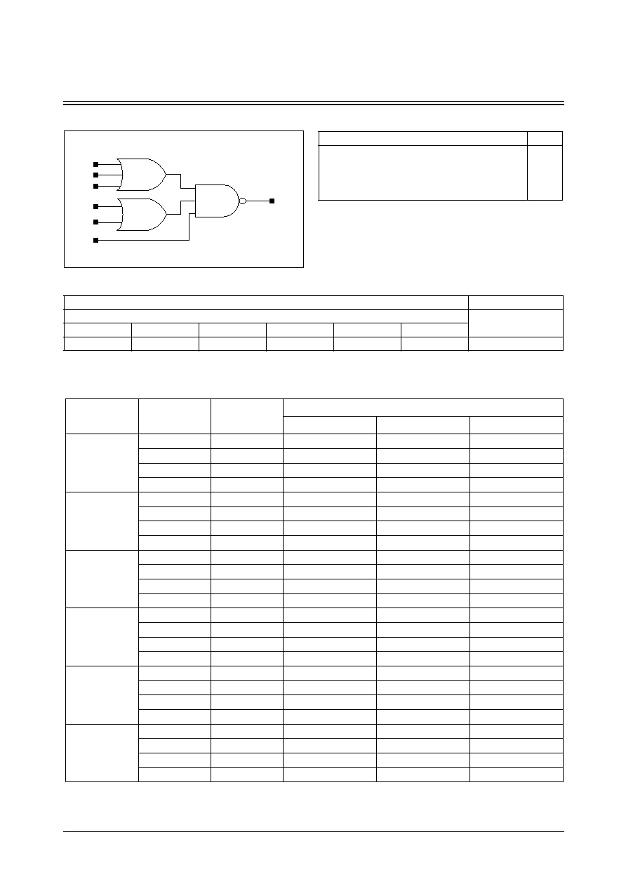
STDL131
3-150
Samsung ASIC
OA321_LP
3-OR and 2-OR into 3-NAND with 1X Drive
Logic Symbol
Cell Data
Switching Characteristics
(Typical process, 25
∞
C, 1.8V, t
R
/t
F
= 0.19ns, SL: Standard Load)
OA321_LP
Input Load (SL)
Gate Count
OA321_LP
OA321_LP
A
B
C
D
E
F
1.0
1.0
1.1
0.9
1.0
0.7
2.67
Truth Table
A
B
C
D
E
F
Y
0
0
0
x
x
x
1
x
x
x
0
0
x
1
x
x
x
x
x
0
1
Other States
0
D
E
Y
A
B
C
F
Path
Parameter
Delay [ns]
SL = 2
Delay Equations [ns]
Group1*
Group2*
Group3*
A to Y
tR
0.485
0.329 + 0.078*SL
0.321 + 0.080*SL
0.321 + 0.080*SL
tF
0.256
0.164 + 0.046*SL
0.159 + 0.047*SL
0.155 + 0.048*SL
tPLH
0.216
0.136 + 0.040*SL
0.137 + 0.040*SL
0.139 + 0.039*SL
tPHL
0.187
0.136 + 0.026*SL
0.139 + 0.025*SL
0.141 + 0.025*SL
B to Y
tR
0.487
0.330 + 0.079*SL
0.326 + 0.080*SL
0.324 + 0.080*SL
tF
0.291
0.198 + 0.047*SL
0.195 + 0.048*SL
0.192 + 0.048*SL
tPLH
0.265
0.185 + 0.040*SL
0.187 + 0.040*SL
0.188 + 0.039*SL
tPHL
0.220
0.168 + 0.026*SL
0.170 + 0.025*SL
0.173 + 0.025*SL
C to Y
tR
0.487
0.329 + 0.079*SL
0.326 + 0.080*SL
0.324 + 0.080*SL
tF
0.326
0.233 + 0.047*SL
0.231 + 0.047*SL
0.230 + 0.047*SL
tPLH
0.286
0.206 + 0.040*SL
0.207 + 0.040*SL
0.209 + 0.039*SL
tPHL
0.239
0.186 + 0.026*SL
0.190 + 0.025*SL
0.194 + 0.025*SL
D to Y
tR
0.338
0.216 + 0.061*SL
0.211 + 0.062*SL
0.209 + 0.063*SL
tF
0.297
0.203 + 0.047*SL
0.201 + 0.048*SL
0.200 + 0.048*SL
tPLH
0.234
0.173 + 0.031*SL
0.174 + 0.030*SL
0.175 + 0.030*SL
tPHL
0.234
0.180 + 0.027*SL
0.184 + 0.026*SL
0.190 + 0.025*SL
E to Y
tR
0.335
0.211 + 0.062*SL
0.210 + 0.062*SL
0.209 + 0.063*SL
tF
0.325
0.231 + 0.047*SL
0.230 + 0.047*SL
0.230 + 0.047*SL
tPLH
0.256
0.195 + 0.031*SL
0.196 + 0.030*SL
0.197 + 0.030*SL
tPHL
0.261
0.208 + 0.027*SL
0.212 + 0.026*SL
0.216 + 0.025*SL
F to Y
tR
0.500
0.403 + 0.049*SL
0.395 + 0.051*SL
0.388 + 0.052*SL
tF
0.325
0.230 + 0.047*SL
0.230 + 0.047*SL
0.230 + 0.047*SL
tPLH
0.227
0.177 + 0.025*SL
0.178 + 0.025*SL
0.180 + 0.024*SL
tPHL
0.265
0.211 + 0.027*SL
0.216 + 0.026*SL
0.220 + 0.025*SL
*Group1 : SL < 4, *Group2 : 4 SL
<
<
=
= 8, *Group3 : 8 < SL

Samsung ASIC
3-151
STDL131
OA322_LP
3-OR and Two 2-ORs into 3-NAND with 1X Drive
Logic Symbol
Cell Data
Input Load (SL)
Gate Count
OA322_LP
OA322_LP
A
B
C
D
E
F
G
1.0
1.0
1.1
1.0
1.1
1.1
1.1
3.33
Truth Table
A
B
C
D
E
F
G
Y
0
0
0
x
x
x
x
1
x
x
x
0
0
x
x
1
x
x
x
x
x
0
0
1
Other States
0
D
E
Y
A
B
F
G
C

STDL131
3-152
Samsung ASIC
OA322_LP
3-OR and Two 2-ORs into 3-NAND with 1X Drive
Switching Characteristics
(Typical process, 25
∞
C, 1.8V, t
R
/t
F
= 0.19ns, SL: Standard Load)
OA322_LP
Path
Parameter
Delay [ns]
SL = 2
Delay Equations [ns]
Group1*
Group2*
Group3*
A to Y
tR
0.643
0.486 + 0.079*SL
0.479 + 0.080*SL
0.480 + 0.080*SL
tF
0.318
0.223 + 0.047*SL
0.221 + 0.048*SL
0.221 + 0.048*SL
tPLH
0.235
0.155 + 0.040*SL
0.156 + 0.040*SL
0.158 + 0.039*SL
tPHL
0.241
0.189 + 0.026*SL
0.192 + 0.025*SL
0.194 + 0.025*SL
B to Y
tR
0.645
0.487 + 0.079*SL
0.484 + 0.080*SL
0.483 + 0.080*SL
tF
0.353
0.258 + 0.048*SL
0.257 + 0.048*SL
0.258 + 0.048*SL
tPLH
0.284
0.204 + 0.040*SL
0.205 + 0.040*SL
0.206 + 0.039*SL
tPHL
0.273
0.221 + 0.026*SL
0.224 + 0.025*SL
0.227 + 0.025*SL
C to Y
tR
0.645
0.486 + 0.079*SL
0.484 + 0.080*SL
0.483 + 0.080*SL
tF
0.388
0.293 + 0.047*SL
0.292 + 0.048*SL
0.294 + 0.047*SL
tPLH
0.304
0.224 + 0.040*SL
0.225 + 0.040*SL
0.226 + 0.039*SL
tPHL
0.293
0.241 + 0.026*SL
0.244 + 0.025*SL
0.248 + 0.025*SL
D to Y
tR
0.463
0.363 + 0.050*SL
0.356 + 0.052*SL
0.347 + 0.053*SL
tF
0.354
0.259 + 0.048*SL
0.258 + 0.048*SL
0.259 + 0.048*SL
tPLH
0.222
0.169 + 0.026*SL
0.170 + 0.026*SL
0.171 + 0.026*SL
tPHL
0.287
0.233 + 0.027*SL
0.237 + 0.026*SL
0.242 + 0.025*SL
E to Y
tR
0.460
0.358 + 0.051*SL
0.353 + 0.052*SL
0.348 + 0.053*SL
tF
0.387
0.292 + 0.048*SL
0.293 + 0.047*SL
0.294 + 0.047*SL
tPLH
0.243
0.190 + 0.026*SL
0.191 + 0.026*SL
0.192 + 0.026*SL
tPHL
0.318
0.265 + 0.026*SL
0.269 + 0.026*SL
0.273 + 0.025*SL
F to Y
tR
0.562
0.461 + 0.051*SL
0.454 + 0.052*SL
0.448 + 0.053*SL
tF
0.351
0.256 + 0.048*SL
0.256 + 0.047*SL
0.257 + 0.047*SL
tPLH
0.250
0.196 + 0.027*SL
0.198 + 0.026*SL
0.200 + 0.026*SL
tPHL
0.296
0.243 + 0.027*SL
0.247 + 0.026*SL
0.252 + 0.025*SL
G to Y
tR
0.559
0.457 + 0.051*SL
0.453 + 0.052*SL
0.448 + 0.053*SL
tF
0.387
0.292 + 0.048*SL
0.292 + 0.048*SL
0.294 + 0.047*SL
tPLH
0.272
0.219 + 0.027*SL
0.220 + 0.026*SL
0.222 + 0.026*SL
tPHL
0.330
0.277 + 0.026*SL
0.281 + 0.025*SL
0.285 + 0.025*SL
*Group1 : SL < 4, *Group2 : 4 SL
<
<
=
= 8, *Group3 : 8 < SL

Samsung ASIC
3-153
STDL131
OA33_LP
Two 3-ORs into 2-NAND with 1X Drive
Logic Symbol
Cell Data
Switching Characteristics
(Typical process, 25
∞
C, 1.8V, t
R
/t
F
= 0.19ns, SL: Standard Load)
OA33_LP
Input Load (SL)
Gate Count
OA33_LP
OA33_LP
A
B
C
D
E
F
1.0
1.0
1.0
1.0
1.0
1.0
2.67
D
F
Y
A
C
E
B
Path
Parameter
Delay [ns]
SL = 2
Delay Equations [ns]
Group1*
Group2*
Group3*
A to Y
tR
0.574
0.421 + 0.076*SL
0.409 + 0.079*SL
0.405 + 0.080*SL
tF
0.242
0.158 + 0.042*SL
0.155 + 0.043*SL
0.151 + 0.043*SL
tPLH
0.197
0.118 + 0.040*SL
0.118 + 0.040*SL
0.119 + 0.039*SL
tPHL
0.193
0.143 + 0.025*SL
0.148 + 0.024*SL
0.153 + 0.023*SL
B to Y
tR
0.463
0.306 + 0.079*SL
0.301 + 0.080*SL
0.298 + 0.080*SL
tF
0.274
0.189 + 0.043*SL
0.187 + 0.043*SL
0.186 + 0.043*SL
tPLH
0.249
0.169 + 0.040*SL
0.170 + 0.039*SL
0.171 + 0.039*SL
tPHL
0.225
0.175 + 0.025*SL
0.180 + 0.024*SL
0.185 + 0.023*SL
C to Y
tR
0.462
0.305 + 0.079*SL
0.301 + 0.080*SL
0.298 + 0.080*SL
tF
0.307
0.221 + 0.043*SL
0.221 + 0.043*SL
0.221 + 0.043*SL
tPLH
0.270
0.191 + 0.040*SL
0.191 + 0.039*SL
0.192 + 0.039*SL
tPHL
0.245
0.194 + 0.026*SL
0.200 + 0.024*SL
0.206 + 0.023*SL
D to Y
tR
0.414
0.253 + 0.080*SL
0.248 + 0.082*SL
0.251 + 0.081*SL
tF
0.243
0.157 + 0.043*SL
0.157 + 0.043*SL
0.156 + 0.043*SL
tPLH
0.253
0.172 + 0.040*SL
0.173 + 0.040*SL
0.175 + 0.040*SL
tPHL
0.208
0.158 + 0.025*SL
0.163 + 0.024*SL
0.169 + 0.023*SL
E to Y
tR
0.416
0.255 + 0.081*SL
0.253 + 0.081*SL
0.253 + 0.081*SL
tF
0.274
0.188 + 0.043*SL
0.188 + 0.043*SL
0.188 + 0.043*SL
tPLH
0.303
0.222 + 0.040*SL
0.224 + 0.040*SL
0.225 + 0.040*SL
tPHL
0.239
0.189 + 0.025*SL
0.194 + 0.024*SL
0.200 + 0.023*SL
F to Y
tR
0.416
0.254 + 0.081*SL
0.253 + 0.081*SL
0.253 + 0.081*SL
tF
0.307
0.221 + 0.043*SL
0.221 + 0.043*SL
0.222 + 0.043*SL
tPLH
0.322
0.242 + 0.040*SL
0.243 + 0.040*SL
0.244 + 0.040*SL
tPHL
0.259
0.208 + 0.026*SL
0.214 + 0.024*SL
0.220 + 0.023*SL
*Group1 : SL < 4, *Group2 : 4 SL
<
<
=
= 8, *Group3 : 8 < SL
Truth Table
A
B
C
D
E
F
Y
0
0
0
x
x
x
1
x
x
x
0
0
0
1
Other States
0

STDL131
3-154
Samsung ASIC
SCG1_LP/SCG1D2_LP
2-NAND and two (2-AND into 2-NOR)s into 3-NAND with 1X/2X Drive
Logic Symbol
Cell Data
Input Load (SL)
Gate Count
SCG1_LP
SCG1_LP
A
B
C
D
E
F
G
H
0.7
0.7
0.7
0.7
0.7
0.7
0.7
0.7
4.67
SCG1D2_LP
SCG1D2_LP
A
B
C
D
E
F
G
H
0.9
0.9
0.7
0.7
0.7
0.7
0.7
0.7
5.67
C
D
E
A
B
F
G
H
Y
Truth Table
A
B
C
D
E
F
G
H
Y
1
1
x
x
x
x
x
x
1
x
x
1
1
x
x
x
x
1
x
x
x
x
1
x
x
x
1
x
x
x
x
x
1
1
x
1
x
x
x
x
x
x
x
1
1
Other States
0
Samsung ASIC
3-155
STDL131
SCG1_LP/SCG1D2_LP
2-NAND and two (2-AND into 2-NOR)s into 3-NAND with 1X/2X Drive
Switching Characteristics
(Typical process, 25
∞
C, 1.8V, t
R
/t
F
= 0.19ns, SL: Standard Load)
SCG1_LP
Path
Parameter
Delay [ns]
SL = 2
Delay Equations [ns]
Group1*
Group2*
Group3*
A to Y
tR
0.149
0.081 + 0.034*SL
0.074 + 0.036*SL
0.071 + 0.036*SL
tF
0.153
0.081 + 0.036*SL
0.078 + 0.037*SL
0.076 + 0.037*SL
tPLH
0.195
0.159 + 0.018*SL
0.163 + 0.017*SL
0.164 + 0.017*SL
tPHL
0.205
0.165 + 0.020*SL
0.167 + 0.019*SL
0.168 + 0.019*SL
B to Y
tR
0.148
0.079 + 0.035*SL
0.075 + 0.036*SL
0.071 + 0.036*SL
tF
0.155
0.083 + 0.036*SL
0.079 + 0.037*SL
0.077 + 0.037*SL
tPLH
0.192
0.156 + 0.018*SL
0.159 + 0.017*SL
0.161 + 0.017*SL
tPHL
0.214
0.174 + 0.020*SL
0.176 + 0.019*SL
0.177 + 0.019*SL
C to Y
tR
0.167
0.098 + 0.034*SL
0.094 + 0.035*SL
0.089 + 0.036*SL
tF
0.164
0.091 + 0.036*SL
0.091 + 0.036*SL
0.088 + 0.037*SL
tPLH
0.243
0.206 + 0.018*SL
0.210 + 0.017*SL
0.212 + 0.017*SL
tPHL
0.260
0.217 + 0.021*SL
0.223 + 0.020*SL
0.228 + 0.019*SL
D to Y
tR
0.167
0.098 + 0.034*SL
0.095 + 0.035*SL
0.089 + 0.036*SL
tF
0.165
0.093 + 0.036*SL
0.091 + 0.036*SL
0.088 + 0.037*SL
tPLH
0.240
0.203 + 0.018*SL
0.207 + 0.017*SL
0.209 + 0.017*SL
tPHL
0.271
0.229 + 0.021*SL
0.235 + 0.020*SL
0.239 + 0.019*SL
E to Y
tR
0.164
0.095 + 0.035*SL
0.091 + 0.035*SL
0.086 + 0.036*SL
tF
0.165
0.094 + 0.036*SL
0.091 + 0.036*SL
0.088 + 0.037*SL
tPLH
0.252
0.216 + 0.018*SL
0.219 + 0.017*SL
0.221 + 0.017*SL
tPHL
0.311
0.268 + 0.021*SL
0.274 + 0.020*SL
0.279 + 0.019*SL
F to Y
tR
0.177
0.108 + 0.035*SL
0.105 + 0.035*SL
0.099 + 0.036*SL
tF
0.160
0.087 + 0.036*SL
0.085 + 0.037*SL
0.084 + 0.037*SL
tPLH
0.248
0.211 + 0.018*SL
0.215 + 0.017*SL
0.217 + 0.017*SL
tPHL
0.257
0.215 + 0.021*SL
0.220 + 0.020*SL
0.224 + 0.019*SL
G to Y
tR
0.177
0.109 + 0.034*SL
0.104 + 0.035*SL
0.100 + 0.036*SL
tF
0.159
0.086 + 0.037*SL
0.086 + 0.037*SL
0.084 + 0.037*SL
tPLH
0.244
0.208 + 0.018*SL
0.212 + 0.017*SL
0.213 + 0.017*SL
tPHL
0.269
0.227 + 0.021*SL
0.232 + 0.020*SL
0.235 + 0.019*SL
H to Y
tR
0.175
0.106 + 0.034*SL
0.101 + 0.036*SL
0.098 + 0.036*SL
tF
0.160
0.088 + 0.036*SL
0.086 + 0.037*SL
0.084 + 0.037*SL
tPLH
0.258
0.222 + 0.018*SL
0.225 + 0.017*SL
0.227 + 0.017*SL
tPHL
0.309
0.267 + 0.021*SL
0.272 + 0.020*SL
0.276 + 0.019*SL
*Group1 : SL < 4, *Group2 : 4 SL
<
<
=
= 8, *Group3 : 8 < SL

STDL131
3-156
Samsung ASIC
SCG1_LP/SCG1D2_LP
2-NAND and two (2-AND into 2-NOR)s into 3-NAND with 1X/2X Drive
Switching Characteristics
(Typical process, 25
∞
C, 1.8V, t
R
/t
F
= 0.19ns, SL: Standard Load)
SCG1D2_LP
Path
Parameter
Delay [ns]
SL = 2
Delay Equations [ns]
Group1*
Group2*
Group3*
A to Y
tR
0.109
0.075 + 0.017*SL
0.073 + 0.017*SL
0.066 + 0.018*SL
tF
0.114
0.078 + 0.018*SL
0.076 + 0.018*SL
0.072 + 0.019*SL
tPLH
0.174
0.154 + 0.010*SL
0.158 + 0.009*SL
0.161 + 0.009*SL
tPHL
0.190
0.169 + 0.011*SL
0.172 + 0.010*SL
0.175 + 0.010*SL
B to Y
tR
0.108
0.074 + 0.017*SL
0.071 + 0.018*SL
0.066 + 0.018*SL
tF
0.114
0.079 + 0.017*SL
0.076 + 0.018*SL
0.073 + 0.019*SL
tPLH
0.170
0.150 + 0.010*SL
0.154 + 0.009*SL
0.157 + 0.009*SL
tPHL
0.200
0.179 + 0.011*SL
0.182 + 0.010*SL
0.184 + 0.010*SL
C to Y
tR
0.137
0.104 + 0.017*SL
0.101 + 0.017*SL
0.095 + 0.018*SL
tF
0.132
0.096 + 0.018*SL
0.097 + 0.018*SL
0.093 + 0.018*SL
tPLH
0.253
0.232 + 0.010*SL
0.237 + 0.009*SL
0.243 + 0.009*SL
tPHL
0.275
0.251 + 0.012*SL
0.257 + 0.011*SL
0.267 + 0.010*SL
D to Y
tR
0.137
0.104 + 0.017*SL
0.102 + 0.017*SL
0.095 + 0.018*SL
tF
0.133
0.098 + 0.018*SL
0.097 + 0.018*SL
0.094 + 0.018*SL
tPLH
0.249
0.228 + 0.010*SL
0.234 + 0.009*SL
0.240 + 0.009*SL
tPHL
0.287
0.263 + 0.012*SL
0.269 + 0.011*SL
0.279 + 0.010*SL
E to Y
tR
0.133
0.100 + 0.017*SL
0.097 + 0.017*SL
0.090 + 0.018*SL
tF
0.133
0.098 + 0.018*SL
0.097 + 0.018*SL
0.094 + 0.018*SL
tPLH
0.264
0.243 + 0.010*SL
0.248 + 0.009*SL
0.252 + 0.009*SL
tPHL
0.327
0.303 + 0.012*SL
0.309 + 0.011*SL
0.319 + 0.010*SL
F to Y
tR
0.148
0.115 + 0.017*SL
0.113 + 0.017*SL
0.107 + 0.018*SL
tF
0.125
0.088 + 0.019*SL
0.090 + 0.018*SL
0.087 + 0.018*SL
tPLH
0.263
0.243 + 0.010*SL
0.247 + 0.009*SL
0.253 + 0.009*SL
tPHL
0.277
0.253 + 0.012*SL
0.258 + 0.011*SL
0.267 + 0.010*SL
G to Y
tR
0.148
0.113 + 0.017*SL
0.114 + 0.017*SL
0.107 + 0.018*SL
tF
0.126
0.089 + 0.018*SL
0.089 + 0.018*SL
0.089 + 0.018*SL
tPLH
0.260
0.240 + 0.010*SL
0.244 + 0.009*SL
0.250 + 0.009*SL
tPHL
0.289
0.265 + 0.012*SL
0.270 + 0.011*SL
0.279 + 0.010*SL
H to Y
tR
0.144
0.110 + 0.017*SL
0.108 + 0.017*SL
0.101 + 0.018*SL
tF
0.126
0.090 + 0.018*SL
0.089 + 0.018*SL
0.089 + 0.018*SL
tPLH
0.274
0.254 + 0.010*SL
0.258 + 0.009*SL
0.262 + 0.009*SL
tPHL
0.329
0.305 + 0.012*SL
0.310 + 0.011*SL
0.319 + 0.010*SL
*Group1 : SL < 4, *Group2 : 4 SL
<
<
=
= 12, *Group3 : 12 < SL
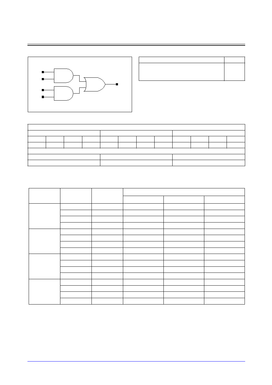
Samsung ASIC
3-157
STDL131
SCG2_LP/SCG2D2_LP/SCG2D4_LP
Two 2-ANDs into 2-OR with 1X/2X4X Drive
Logic Symbol
Cell Data
Switching Characteristics
(Typical process, 25
∞
C, 1.8V, t
R
/t
F
= 0.19ns, SL: Standard Load)
SCG2_LP
Input Load (SL)
SCG2_LP
SCG2D2_LP
SCG2D4_LP
A
B
C
D
A
B
C
D
A
B
C
D
0.9
0.9
0.9
1.0
1.0
1.0
1.0
1.1
1.0
1.1
1.0
1.1
Gate Count
SCG2_LP
SCG2D2_LP
SCG2D4_LP
2.33
2.67
3.33
C
D
A
B
Y
Path
Parameter
Delay [ns]
SL = 2
Delay Equations [ns]
Group1*
Group2*
Group3*
A to Y
tR
0.112
0.063 + 0.024*SL
0.060 + 0.025*SL
0.055 + 0.026*SL
tF
0.090
0.054 + 0.018*SL
0.056 + 0.017*SL
0.060 + 0.017*SL
tPLH
0.205
0.174 + 0.016*SL
0.184 + 0.013*SL
0.189 + 0.013*SL
tPHL
0.210
0.181 + 0.015*SL
0.192 + 0.012*SL
0.203 + 0.010*SL
B to Y
tR
0.112
0.063 + 0.025*SL
0.060 + 0.025*SL
0.055 + 0.026*SL
tF
0.091
0.055 + 0.018*SL
0.061 + 0.017*SL
0.060 + 0.017*SL
tPLH
0.202
0.170 + 0.016*SL
0.180 + 0.013*SL
0.185 + 0.013*SL
tPHL
0.219
0.189 + 0.015*SL
0.201 + 0.012*SL
0.211 + 0.010*SL
C to Y
tR
0.117
0.068 + 0.025*SL
0.067 + 0.025*SL
0.059 + 0.026*SL
tF
0.089
0.052 + 0.019*SL
0.059 + 0.017*SL
0.059 + 0.017*SL
tPLH
0.276
0.244 + 0.016*SL
0.254 + 0.014*SL
0.260 + 0.013*SL
tPHL
0.261
0.232 + 0.015*SL
0.243 + 0.012*SL
0.254 + 0.010*SL
D to Y
tR
0.118
0.069 + 0.025*SL
0.066 + 0.025*SL
0.060 + 0.026*SL
tF
0.091
0.056 + 0.018*SL
0.060 + 0.017*SL
0.060 + 0.017*SL
tPLH
0.273
0.241 + 0.016*SL
0.251 + 0.014*SL
0.257 + 0.013*SL
tPHL
0.271
0.241 + 0.015*SL
0.253 + 0.012*SL
0.263 + 0.010*SL
*Group1 : SL < 4, *Group2 : 4 SL
<
<
=
= 8, *Group3 : 8 < SL
Truth Table
A
B
C
D
Y
1
1
x
x
1
x
x
1
1
1
Other States
0
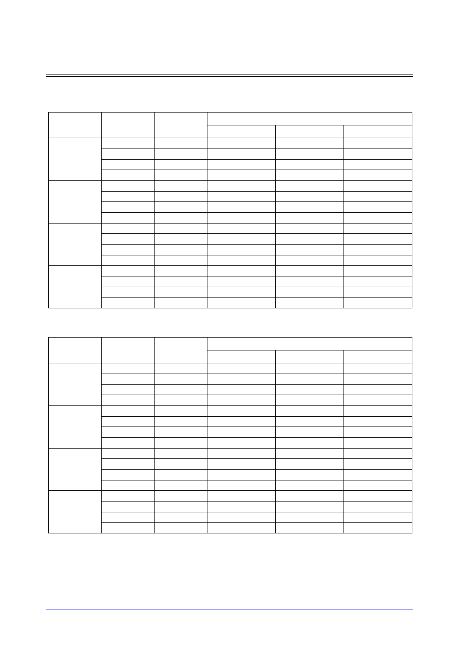
STDL131
3-158
Samsung ASIC
SCG2_LP/SCG2D2_LP/SCG2D4_LP
Two 2-ANDs into 2-OR with 1X/2X/4X Drive
Switching Characteristics
(Typical process, 25
∞
C, 1.8V, t
R
/t
F
= 0.19ns, SL: Standard Load)
SCG2D2_LP
SCG2D4_LP
Path
Parameter
Delay [ns]
SL = 2
Delay Equations [ns]
Group1*
Group2*
Group3*
A to Y
tR
0.087
0.061 + 0.013*SL
0.064 + 0.012*SL
0.058 + 0.013*SL
tF
0.080
0.059 + 0.011*SL
0.065 + 0.009*SL
0.071 + 0.008*SL
tPLH
0.196
0.176 + 0.010*SL
0.186 + 0.008*SL
0.198 + 0.006*SL
tPHL
0.229
0.209 + 0.010*SL
0.220 + 0.007*SL
0.238 + 0.006*SL
B to Y
tR
0.086
0.059 + 0.014*SL
0.064 + 0.012*SL
0.058 + 0.013*SL
tF
0.080
0.058 + 0.011*SL
0.067 + 0.009*SL
0.072 + 0.008*SL
tPLH
0.192
0.172 + 0.010*SL
0.182 + 0.008*SL
0.194 + 0.006*SL
tPHL
0.239
0.219 + 0.010*SL
0.230 + 0.007*SL
0.249 + 0.006*SL
C to Y
tR
0.090
0.065 + 0.013*SL
0.067 + 0.012*SL
0.062 + 0.013*SL
tF
0.079
0.057 + 0.011*SL
0.066 + 0.009*SL
0.071 + 0.008*SL
tPLH
0.252
0.231 + 0.010*SL
0.241 + 0.008*SL
0.254 + 0.007*SL
tPHL
0.281
0.261 + 0.010*SL
0.272 + 0.007*SL
0.290 + 0.006*SL
D to Y
tR
0.090
0.064 + 0.013*SL
0.067 + 0.012*SL
0.062 + 0.013*SL
tF
0.080
0.060 + 0.010*SL
0.066 + 0.009*SL
0.071 + 0.008*SL
tPLH
0.248
0.228 + 0.010*SL
0.238 + 0.008*SL
0.250 + 0.007*SL
tPHL
0.292
0.272 + 0.010*SL
0.283 + 0.007*SL
0.301 + 0.006*SL
*Group1 : SL < 4, *Group2 : 4 SL
<
<
=
= 12, *Group3 : 12 < SL
Path
Parameter
Delay [ns]
SL = 2
Delay Equations [ns]
Group1*
Group2*
Group3*
A to Y
tR
0.088
0.072 + 0.008*SL
0.079 + 0.006*SL
0.082 + 0.006*SL
tF
0.091
0.079 + 0.006*SL
0.084 + 0.005*SL
0.097 + 0.004*SL
tPLH
0.233
0.220 + 0.007*SL
0.229 + 0.005*SL
0.251 + 0.003*SL
tPHL
0.284
0.271 + 0.007*SL
0.280 + 0.004*SL
0.307 + 0.003*SL
B to Y
tR
0.090
0.074 + 0.008*SL
0.079 + 0.006*SL
0.082 + 0.006*SL
tF
0.093
0.079 + 0.007*SL
0.087 + 0.005*SL
0.100 + 0.004*SL
tPLH
0.230
0.216 + 0.007*SL
0.225 + 0.005*SL
0.247 + 0.003*SL
tPHL
0.294
0.280 + 0.007*SL
0.289 + 0.004*SL
0.317 + 0.003*SL
C to Y
tR
0.093
0.078 + 0.008*SL
0.082 + 0.006*SL
0.085 + 0.006*SL
tF
0.090
0.077 + 0.006*SL
0.084 + 0.005*SL
0.098 + 0.004*SL
tPLH
0.291
0.277 + 0.007*SL
0.286 + 0.005*SL
0.308 + 0.003*SL
tPHL
0.337
0.323 + 0.007*SL
0.332 + 0.004*SL
0.359 + 0.003*SL
D to Y
tR
0.093
0.078 + 0.007*SL
0.082 + 0.006*SL
0.085 + 0.006*SL
tF
0.092
0.079 + 0.007*SL
0.087 + 0.005*SL
0.099 + 0.004*SL
tPLH
0.287
0.274 + 0.007*SL
0.282 + 0.005*SL
0.305 + 0.003*SL
tPHL
0.346
0.333 + 0.007*SL
0.342 + 0.004*SL
0.369 + 0.003*SL
*Group1 : SL < 4, *Group2 : 4 SL
<
<
=
= 20, *Group3 : 20 < SL
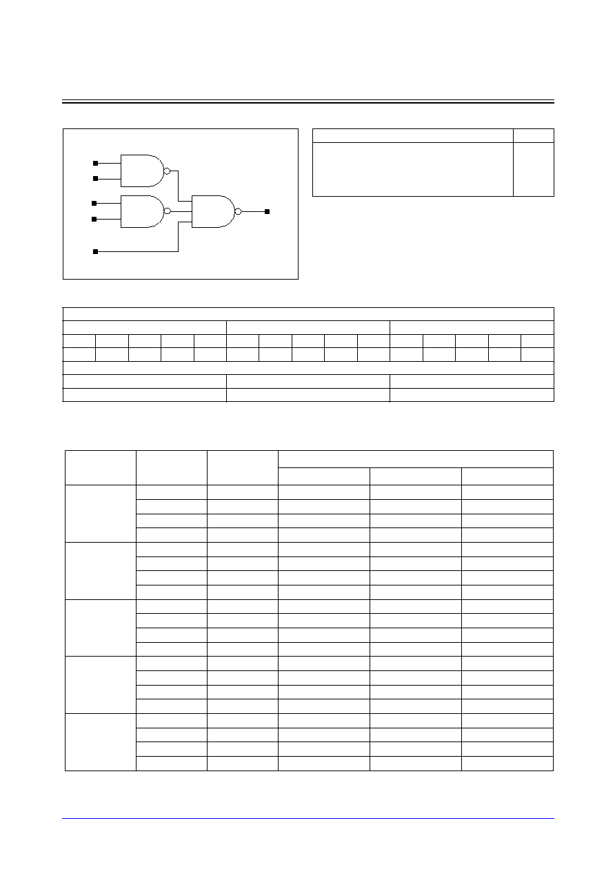
Samsung ASIC
3-159
STDL131
SCG3_LP/SCG3D2_LP/SCG3D4_LP
Two 2-NANDs into 3-NAND with 1X/2X/4X Drive
Logic Symbol
Cell Data
Switching Characteristics
(Typical process, 25
∞
C, 1.8V, t
R
/t
F
= 0.19ns, SL: Standard Load)
SCG3_LP
Input Load (SL)
SCG3_LP
SCG3D2_LP
SCG3D4_LP
A
B
C
D
E
A
B
C
D
E
A
B
C
D
E
0.8
0.8
0.8
0.8
1.0
1.0
1.1
1.1
1.1
1.9
0.8
0.8
0.8
0.8
1.0
Gate Count
SCG3_LP
SCG3D2_LP
SCG3D4_LP
3.00
3.67
4.67
A
B
Y
C
D
E
Path
Parameter
Delay [ns]
SL = 2
Delay Equations [ns]
Group1*
Group2*
Group3*
A to Y
tR
0.152
0.084 + 0.034*SL
0.078 + 0.036*SL
0.073 + 0.036*SL
tF
0.152
0.079 + 0.036*SL
0.076 + 0.037*SL
0.074 + 0.037*SL
tPLH
0.212
0.175 + 0.018*SL
0.179 + 0.017*SL
0.181 + 0.017*SL
tPHL
0.192
0.152 + 0.020*SL
0.154 + 0.019*SL
0.154 + 0.019*SL
B to Y
tR
0.151
0.082 + 0.035*SL
0.079 + 0.035*SL
0.073 + 0.036*SL
tF
0.152
0.080 + 0.036*SL
0.077 + 0.037*SL
0.074 + 0.037*SL
tPLH
0.208
0.172 + 0.018*SL
0.176 + 0.017*SL
0.177 + 0.017*SL
tPHL
0.198
0.158 + 0.020*SL
0.160 + 0.019*SL
0.161 + 0.019*SL
C to Y
tR
0.162
0.093 + 0.034*SL
0.088 + 0.036*SL
0.083 + 0.036*SL
tF
0.151
0.077 + 0.037*SL
0.076 + 0.037*SL
0.074 + 0.038*SL
tPLH
0.220
0.184 + 0.018*SL
0.187 + 0.017*SL
0.188 + 0.017*SL
tPHL
0.198
0.158 + 0.020*SL
0.160 + 0.019*SL
0.161 + 0.019*SL
D to Y
tR
0.161
0.092 + 0.035*SL
0.088 + 0.036*SL
0.083 + 0.036*SL
tF
0.151
0.077 + 0.037*SL
0.076 + 0.037*SL
0.073 + 0.038*SL
tPLH
0.217
0.181 + 0.018*SL
0.184 + 0.017*SL
0.185 + 0.017*SL
tPHL
0.205
0.165 + 0.020*SL
0.167 + 0.019*SL
0.168 + 0.019*SL
E to Y
tR
0.175
0.109 + 0.033*SL
0.102 + 0.035*SL
0.093 + 0.036*SL
tF
0.156
0.083 + 0.036*SL
0.080 + 0.037*SL
0.077 + 0.037*SL
tPLH
0.144
0.109 + 0.017*SL
0.110 + 0.017*SL
0.111 + 0.017*SL
tPHL
0.123
0.082 + 0.020*SL
0.085 + 0.020*SL
0.086 + 0.019*SL
*Group1 : SL < 4, *Group2 : 4 SL
<
<
=
= 8, *Group3 : 8 < SL
Truth Table
A
B
C
D
E
Y
1
1
x
x
x
1
x
x
1
1
x
1
x
x
x
x
0
1
Other States
0

STDL131
3-160
Samsung ASIC
SCG3_LP/SCG3D2_LP/SCG3D4_LP
Two 2-NANDs into 3-NAND with 1X/2X/4X Drive
Switching Characteristics
(Typical process, 25
∞
C, 1.8V, t
R
/t
F
= 0.19ns, SL: Standard Load)
SCG3D2_LP
Path
Parameter
Delay [ns]
SL = 2
Delay Equations [ns]
Group1*
Group2*
Group3*
A to Y
tR
0.112
0.078 + 0.017*SL
0.076 + 0.017*SL
0.069 + 0.018*SL
tF
0.110
0.074 + 0.018*SL
0.073 + 0.018*SL
0.069 + 0.019*SL
tPLH
0.193
0.173 + 0.010*SL
0.178 + 0.009*SL
0.182 + 0.009*SL
tPHL
0.177
0.156 + 0.010*SL
0.159 + 0.010*SL
0.161 + 0.010*SL
B to Y
tR
0.112
0.078 + 0.017*SL
0.076 + 0.017*SL
0.069 + 0.018*SL
tF
0.110
0.073 + 0.018*SL
0.074 + 0.018*SL
0.069 + 0.019*SL
tPLH
0.189
0.169 + 0.010*SL
0.173 + 0.009*SL
0.178 + 0.009*SL
tPHL
0.184
0.163 + 0.010*SL
0.166 + 0.010*SL
0.167 + 0.010*SL
C to Y
tR
0.124
0.090 + 0.017*SL
0.087 + 0.017*SL
0.080 + 0.018*SL
tF
0.108
0.071 + 0.018*SL
0.070 + 0.018*SL
0.068 + 0.019*SL
tPLH
0.206
0.187 + 0.010*SL
0.190 + 0.009*SL
0.194 + 0.009*SL
tPHL
0.186
0.165 + 0.011*SL
0.168 + 0.010*SL
0.170 + 0.010*SL
D to Y
tR
0.123
0.090 + 0.017*SL
0.087 + 0.017*SL
0.080 + 0.018*SL
tF
0.107
0.071 + 0.018*SL
0.070 + 0.018*SL
0.068 + 0.019*SL
tPLH
0.202
0.182 + 0.010*SL
0.186 + 0.009*SL
0.189 + 0.009*SL
tPHL
0.193
0.172 + 0.011*SL
0.175 + 0.010*SL
0.177 + 0.010*SL
E to Y
tR
0.136
0.105 + 0.016*SL
0.100 + 0.017*SL
0.089 + 0.018*SL
tF
0.113
0.078 + 0.017*SL
0.075 + 0.018*SL
0.071 + 0.019*SL
tPLH
0.123
0.105 + 0.009*SL
0.106 + 0.009*SL
0.107 + 0.009*SL
tPHL
0.097
0.075 + 0.011*SL
0.079 + 0.010*SL
0.082 + 0.010*SL
*Group1 : SL < 4, *Group2 : 4 SL
<
<
=
= 12, *Group3 : 12 < SL

Samsung ASIC
3-161
STDL131
SCG3_LP/SCG3D2_LP/SCG3D4_LP
Two 2-NANDs into 3-NAND with 1X/2X/4X Drive
Switching Characteristics
(Typical process, 25
∞
C, 1.8V, t
R
/t
F
= 0.19ns, SL: Standard Load)
SCG3D4_LP
Path
Parameter
Delay [ns]
SL = 2
Delay Equations [ns]
Group1*
Group2*
Group3*
A to Y
tR
0.059
0.045 + 0.007*SL
0.049 + 0.006*SL
0.041 + 0.007*SL
tF
0.056
0.047 + 0.005*SL
0.049 + 0.004*SL
0.051 + 0.004*SL
tPLH
0.333
0.323 + 0.005*SL
0.328 + 0.004*SL
0.336 + 0.003*SL
tPHL
0.335
0.325 + 0.005*SL
0.332 + 0.003*SL
0.346 + 0.003*SL
B to Y
tR
0.061
0.050 + 0.006*SL
0.048 + 0.006*SL
0.039 + 0.007*SL
tF
0.057
0.048 + 0.004*SL
0.048 + 0.004*SL
0.050 + 0.004*SL
tPLH
0.329
0.319 + 0.005*SL
0.324 + 0.004*SL
0.331 + 0.003*SL
tPHL
0.342
0.332 + 0.005*SL
0.338 + 0.003*SL
0.353 + 0.003*SL
C to Y
tR
0.061
0.049 + 0.006*SL
0.049 + 0.006*SL
0.040 + 0.007*SL
tF
0.057
0.047 + 0.005*SL
0.050 + 0.004*SL
0.051 + 0.004*SL
tPLH
0.347
0.337 + 0.005*SL
0.342 + 0.004*SL
0.350 + 0.003*SL
tPHL
0.344
0.334 + 0.005*SL
0.340 + 0.003*SL
0.355 + 0.003*SL
D to Y
tR
0.060
0.046 + 0.007*SL
0.049 + 0.006*SL
0.041 + 0.007*SL
tF
0.056
0.047 + 0.005*SL
0.050 + 0.004*SL
0.051 + 0.004*SL
tPLH
0.344
0.335 + 0.005*SL
0.340 + 0.004*SL
0.347 + 0.003*SL
tPHL
0.351
0.341 + 0.005*SL
0.347 + 0.003*SL
0.362 + 0.003*SL
E to Y
tR
0.060
0.046 + 0.007*SL
0.049 + 0.006*SL
0.041 + 0.007*SL
tF
0.057
0.048 + 0.004*SL
0.049 + 0.004*SL
0.050 + 0.004*SL
tPLH
0.268
0.259 + 0.005*SL
0.264 + 0.004*SL
0.271 + 0.003*SL
tPHL
0.268
0.259 + 0.005*SL
0.265 + 0.003*SL
0.279 + 0.003*SL
*Group1 : SL < 4, *Group2 : 4 SL
<
<
=
= 20, *Group3 : 20 < SL
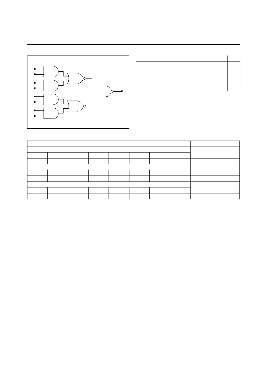
STDL131
3-162
Samsung ASIC
SCG4_LP/SCG4D2_LP/SCG4D4_LP
Two (two 2-ANDs into 2-NOR)s into 2-NAND with 1X/2X/4X Drive
Logic Symbol
Cell Data
Input Load (SL)
Gate Count
SCG4_LP
SCG4_LP
A
B
C
D
E
F
G
H
0.8
0.8
0.8
0.8
0.8
0.8
0.8
0.8
3.67
SCG4D2_LP
SCG4D2_LP
A
B
C
D
E
F
G
H
1.1
1.1
1.1
1.1
1.0
1.1
1.1
1.1
5.00
SCG4D4_LP
SCG4D4_LP
A
B
C
D
E
F
G
H
1.1
1.1
1.1
1.1
1.1
1.1
1.1
1.1
6.33
C
D
A
B
G
H
E
F
Y
Truth Table
A
B
C
D
E
F
G
H
Y
1
1
x
x
x
x
x
x
1
x
x
1
1
x
x
x
x
1
x
x
x
x
1
1
x
x
1
x
x
x
x
x
x
1
1
1
Other States
0

Samsung ASIC
3-163
STDL131
SCG4_LP/SCG4D2_LP/SCG4D4_LP
Two (two 2-ANDs into 2-NOR)s into 2-NAND with 1X/2X/4X Drive
Switching Characteristics
(Typical process, 25
∞
C, 1.8V, t
R
/t
F
= 0.19ns, SL: Standard Load)
SCG4_LP
Path
Parameter
Delay [ns]
SL = 2
Delay Equations [ns]
Group1*
Group2*
Group3*
A to Y
tR
0.123
0.075 + 0.024*SL
0.072 + 0.025*SL
0.066 + 0.026*SL
tF
0.133
0.081 + 0.026*SL
0.083 + 0.025*SL
0.082 + 0.025*SL
tPLH
0.212
0.182 + 0.015*SL
0.190 + 0.013*SL
0.195 + 0.013*SL
tPHL
0.259
0.223 + 0.018*SL
0.233 + 0.016*SL
0.242 + 0.014*SL
B to Y
tR
0.123
0.075 + 0.024*SL
0.072 + 0.025*SL
0.066 + 0.026*SL
tF
0.133
0.082 + 0.026*SL
0.085 + 0.025*SL
0.081 + 0.026*SL
tPLH
0.208
0.177 + 0.015*SL
0.185 + 0.013*SL
0.190 + 0.013*SL
tPHL
0.271
0.234 + 0.018*SL
0.244 + 0.016*SL
0.254 + 0.014*SL
C to Y
tR
0.124
0.076 + 0.024*SL
0.072 + 0.025*SL
0.067 + 0.026*SL
tF
0.133
0.081 + 0.026*SL
0.083 + 0.025*SL
0.082 + 0.025*SL
tPLH
0.258
0.228 + 0.015*SL
0.236 + 0.013*SL
0.241 + 0.013*SL
tPHL
0.303
0.267 + 0.018*SL
0.277 + 0.016*SL
0.287 + 0.014*SL
D to Y
tR
0.125
0.077 + 0.024*SL
0.074 + 0.025*SL
0.068 + 0.026*SL
tF
0.134
0.082 + 0.026*SL
0.085 + 0.025*SL
0.082 + 0.025*SL
tPLH
0.257
0.227 + 0.015*SL
0.235 + 0.013*SL
0.239 + 0.013*SL
tPHL
0.316
0.279 + 0.018*SL
0.289 + 0.016*SL
0.299 + 0.014*SL
E to Y
tR
0.130
0.081 + 0.024*SL
0.078 + 0.025*SL
0.073 + 0.026*SL
tF
0.121
0.070 + 0.026*SL
0.070 + 0.026*SL
0.068 + 0.026*SL
tPLH
0.218
0.189 + 0.015*SL
0.195 + 0.013*SL
0.198 + 0.013*SL
tPHL
0.251
0.218 + 0.017*SL
0.225 + 0.015*SL
0.231 + 0.014*SL
F to Y
tR
0.132
0.081 + 0.025*SL
0.082 + 0.025*SL
0.074 + 0.026*SL
tF
0.122
0.072 + 0.025*SL
0.071 + 0.026*SL
0.069 + 0.026*SL
tPLH
0.213
0.183 + 0.015*SL
0.190 + 0.013*SL
0.194 + 0.013*SL
tPHL
0.264
0.230 + 0.017*SL
0.238 + 0.015*SL
0.244 + 0.014*SL
G to Y
tR
0.138
0.089 + 0.024*SL
0.086 + 0.025*SL
0.079 + 0.026*SL
tF
0.121
0.070 + 0.026*SL
0.070 + 0.026*SL
0.068 + 0.026*SL
tPLH
0.258
0.228 + 0.015*SL
0.235 + 0.013*SL
0.240 + 0.013*SL
tPHL
0.297
0.263 + 0.017*SL
0.270 + 0.015*SL
0.276 + 0.014*SL
H to Y
tR
0.136
0.086 + 0.025*SL
0.085 + 0.025*SL
0.081 + 0.026*SL
tF
0.122
0.071 + 0.026*SL
0.071 + 0.026*SL
0.069 + 0.026*SL
tPLH
0.257
0.226 + 0.015*SL
0.233 + 0.013*SL
0.238 + 0.013*SL
tPHL
0.309
0.275 + 0.017*SL
0.283 + 0.015*SL
0.289 + 0.014*SL
*Group1 : SL < 4, *Group2 : 4 SL
<
<
=
= 8, *Group3 : 8 < SL

STDL131
3-164
Samsung ASIC
SCG4_LP/SCG4D2_LP/SCG4D4_LP
Two (two 2-ANDs into 2-NOR)s into 2-NAND with 1X/2X/4X Drive
Switching Characteristics
(Typical process, 25
∞
C, 1.8V, t
R
/t
F
= 0.19ns, SL: Standard Load)
SCG4D2_LP
Path
Parameter
Delay [ns]
SL = 2
Delay Equations [ns]
Group1*
Group2*
Group3*
A to Y
tR
0.098
0.074 + 0.012*SL
0.073 + 0.012*SL
0.067 + 0.013*SL
tF
0.109
0.081 + 0.014*SL
0.084 + 0.013*SL
0.086 + 0.013*SL
tPLH
0.197
0.179 + 0.009*SL
0.186 + 0.007*SL
0.195 + 0.006*SL
tPHL
0.253
0.231 + 0.011*SL
0.240 + 0.009*SL
0.254 + 0.008*SL
B to Y
tR
0.097
0.072 + 0.013*SL
0.074 + 0.012*SL
0.067 + 0.013*SL
tF
0.110
0.081 + 0.014*SL
0.087 + 0.013*SL
0.088 + 0.013*SL
tPLH
0.194
0.176 + 0.009*SL
0.183 + 0.007*SL
0.192 + 0.006*SL
tPHL
0.266
0.244 + 0.011*SL
0.253 + 0.009*SL
0.268 + 0.008*SL
C to Y
tR
0.101
0.077 + 0.012*SL
0.075 + 0.012*SL
0.069 + 0.013*SL
tF
0.109
0.081 + 0.014*SL
0.085 + 0.013*SL
0.086 + 0.013*SL
tPLH
0.246
0.229 + 0.009*SL
0.236 + 0.007*SL
0.245 + 0.006*SL
tPHL
0.306
0.284 + 0.011*SL
0.292 + 0.009*SL
0.307 + 0.008*SL
D to Y
tR
0.101
0.077 + 0.012*SL
0.075 + 0.012*SL
0.070 + 0.013*SL
tF
0.110
0.083 + 0.014*SL
0.086 + 0.013*SL
0.087 + 0.013*SL
tPLH
0.243
0.225 + 0.009*SL
0.232 + 0.007*SL
0.241 + 0.006*SL
tPHL
0.320
0.298 + 0.011*SL
0.306 + 0.009*SL
0.321 + 0.008*SL
E to Y
tR
0.109
0.084 + 0.012*SL
0.084 + 0.012*SL
0.078 + 0.013*SL
tF
0.099
0.071 + 0.014*SL
0.074 + 0.013*SL
0.072 + 0.013*SL
tPLH
0.211
0.193 + 0.009*SL
0.199 + 0.007*SL
0.208 + 0.006*SL
tPHL
0.258
0.239 + 0.010*SL
0.245 + 0.008*SL
0.255 + 0.007*SL
F to Y
tR
0.109
0.084 + 0.012*SL
0.083 + 0.012*SL
0.078 + 0.013*SL
tF
0.099
0.071 + 0.014*SL
0.076 + 0.013*SL
0.073 + 0.013*SL
tPLH
0.208
0.190 + 0.009*SL
0.196 + 0.007*SL
0.205 + 0.006*SL
tPHL
0.271
0.251 + 0.010*SL
0.257 + 0.008*SL
0.268 + 0.007*SL
G to Y
tR
0.113
0.089 + 0.012*SL
0.088 + 0.012*SL
0.084 + 0.013*SL
tF
0.098
0.071 + 0.013*SL
0.073 + 0.013*SL
0.072 + 0.013*SL
tPLH
0.251
0.233 + 0.009*SL
0.240 + 0.007*SL
0.249 + 0.007*SL
tPHL
0.301
0.281 + 0.010*SL
0.287 + 0.008*SL
0.298 + 0.007*SL
H to Y
tR
0.114
0.089 + 0.012*SL
0.088 + 0.012*SL
0.084 + 0.013*SL
tF
0.099
0.072 + 0.014*SL
0.076 + 0.013*SL
0.073 + 0.013*SL
tPLH
0.252
0.235 + 0.009*SL
0.241 + 0.007*SL
0.250 + 0.007*SL
tPHL
0.319
0.300 + 0.010*SL
0.306 + 0.008*SL
0.316 + 0.007*SL
*Group1 : SL < 4, *Group2 : 4 SL
<
<
=
= 12, *Group3 : 12 < SL

Samsung ASIC
3-165
STDL131
SCG4_LP/SCG4D2_LP/SCG4D4_LP
Two (two 2-ANDs into 2-NOR)s into 2-NAND with 1X/2X/4X Drive
Switching Characteristics
(Typical process, 25
∞
C, 1.8V, t
R
/t
F
= 0.19ns, SL: Standard Load)
SCG4D4_LP
Path
Parameter
Delay [ns]
SL = 2
Delay Equations [ns]
Group1*
Group2*
Group3*
A to Y
tR
0.103
0.089 + 0.007*SL
0.092 + 0.006*SL
0.088 + 0.006*SL
tF
0.121
0.104 + 0.008*SL
0.110 + 0.007*SL
0.117 + 0.006*SL
tPLH
0.234
0.223 + 0.006*SL
0.229 + 0.004*SL
0.246 + 0.003*SL
tPHL
0.322
0.308 + 0.007*SL
0.315 + 0.005*SL
0.338 + 0.004*SL
B to Y
tR
0.103
0.089 + 0.007*SL
0.092 + 0.006*SL
0.090 + 0.006*SL
tF
0.123
0.108 + 0.008*SL
0.112 + 0.007*SL
0.118 + 0.006*SL
tPLH
0.231
0.220 + 0.006*SL
0.226 + 0.004*SL
0.243 + 0.003*SL
tPHL
0.334
0.320 + 0.007*SL
0.327 + 0.005*SL
0.350 + 0.004*SL
C to Y
tR
0.105
0.091 + 0.007*SL
0.094 + 0.006*SL
0.091 + 0.006*SL
tF
0.121
0.106 + 0.007*SL
0.109 + 0.007*SL
0.116 + 0.006*SL
tPLH
0.283
0.272 + 0.006*SL
0.278 + 0.004*SL
0.295 + 0.003*SL
tPHL
0.374
0.360 + 0.007*SL
0.367 + 0.005*SL
0.390 + 0.004*SL
D to Y
tR
0.105
0.092 + 0.007*SL
0.095 + 0.006*SL
0.091 + 0.006*SL
tF
0.123
0.107 + 0.008*SL
0.112 + 0.007*SL
0.118 + 0.006*SL
tPLH
0.280
0.269 + 0.006*SL
0.275 + 0.004*SL
0.291 + 0.003*SL
tPHL
0.388
0.374 + 0.007*SL
0.381 + 0.005*SL
0.404 + 0.004*SL
E to Y
tR
0.114
0.100 + 0.007*SL
0.103 + 0.006*SL
0.100 + 0.006*SL
tF
0.107
0.094 + 0.007*SL
0.094 + 0.007*SL
0.097 + 0.006*SL
tPLH
0.249
0.238 + 0.005*SL
0.243 + 0.004*SL
0.258 + 0.003*SL
tPHL
0.323
0.311 + 0.006*SL
0.317 + 0.005*SL
0.334 + 0.004*SL
F to Y
tR
0.113
0.099 + 0.007*SL
0.102 + 0.006*SL
0.101 + 0.006*SL
tF
0.109
0.096 + 0.007*SL
0.097 + 0.007*SL
0.099 + 0.006*SL
tPLH
0.246
0.235 + 0.005*SL
0.240 + 0.004*SL
0.255 + 0.003*SL
tPHL
0.337
0.324 + 0.006*SL
0.330 + 0.005*SL
0.348 + 0.004*SL
G to Y
tR
0.118
0.103 + 0.007*SL
0.107 + 0.006*SL
0.105 + 0.006*SL
tF
0.108
0.094 + 0.007*SL
0.095 + 0.007*SL
0.098 + 0.006*SL
tPLH
0.289
0.278 + 0.005*SL
0.282 + 0.004*SL
0.298 + 0.003*SL
tPHL
0.366
0.354 + 0.006*SL
0.359 + 0.005*SL
0.377 + 0.004*SL
H to Y
tR
0.117
0.103 + 0.007*SL
0.106 + 0.006*SL
0.105 + 0.006*SL
tF
0.110
0.097 + 0.007*SL
0.098 + 0.007*SL
0.100 + 0.006*SL
tPLH
0.291
0.280 + 0.005*SL
0.284 + 0.004*SL
0.300 + 0.003*SL
tPHL
0.386
0.373 + 0.006*SL
0.379 + 0.005*SL
0.396 + 0.004*SL
*Group1 : SL < 4, *Group2 : 4 SL
<
<
=
= 20, *Group3 : 20 < SL
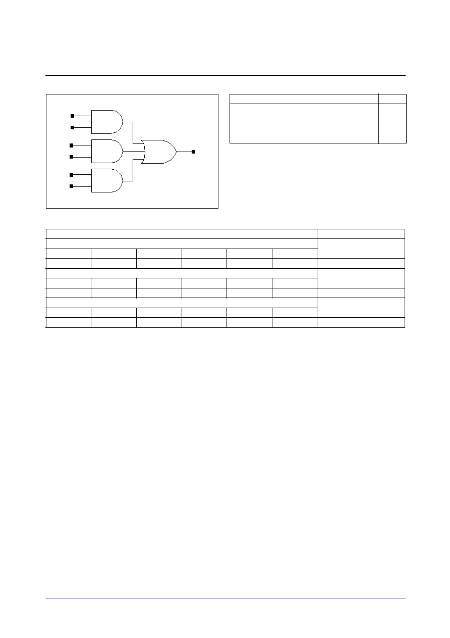
STDL131
3-166
Samsung ASIC
SCG5_LP/SCG5D2_LP/SCG5D4_LP
Three 2-ANDs into 3-OR with 1X/2X/4X Drive
Logic Symbol
Cell Data
Input Load (SL)
Gate Count
SCG5_LP
SCG5_LP
A
B
C
D
E
F
0.8
0.8
0.8
0.8
0.9
0.8
3.00
SCG5D2_LP
SCG5D2_LP
A
B
C
D
E
F
0.9
0.9
0.9
0.9
1.0
0.9
3.67
SCG5D4_LP
SCG5D4_LP
A
B
C
D
E
F
0.9
1.0
1.0
1.0
1.0
1.0
4.00
A
B
Y
C
D
E
F
Truth Table
A
B
C
D
E
F
Y
1
1
x
x
x
x
1
x
x
1
1
x
x
1
x
x
x
x
1
1
1
Other States
0

Samsung ASIC
3-167
STDL131
SCG5_LP/SCG5D2_LP/SCG5D4_LP
Three 2-ANDs into 3-OR with 1X/2X/4X Drive
Switching Characteristics
(Typical process, 25
∞
C, 1.8V, t
R
/t
F
= 0.19ns, SL: Standard Load)
SCG5_LP
Path
Parameter
Delay [ns]
SL = 2
Delay Equations [ns]
Group1*
Group2*
Group3*
A to Y
tR
0.132
0.084 + 0.024*SL
0.081 + 0.025*SL
0.077 + 0.025*SL
tF
0.120
0.080 + 0.020*SL
0.090 + 0.018*SL
0.096 + 0.017*SL
tPLH
0.246
0.211 + 0.017*SL
0.224 + 0.014*SL
0.233 + 0.013*SL
tPHL
0.276
0.242 + 0.017*SL
0.256 + 0.014*SL
0.272 + 0.012*SL
B to Y
tR
0.132
0.083 + 0.024*SL
0.084 + 0.024*SL
0.077 + 0.025*SL
tF
0.122
0.081 + 0.020*SL
0.091 + 0.018*SL
0.099 + 0.017*SL
tPLH
0.242
0.208 + 0.017*SL
0.221 + 0.014*SL
0.230 + 0.013*SL
tPHL
0.290
0.255 + 0.017*SL
0.269 + 0.014*SL
0.286 + 0.012*SL
C to Y
tR
0.135
0.085 + 0.025*SL
0.087 + 0.024*SL
0.081 + 0.025*SL
tF
0.121
0.080 + 0.021*SL
0.092 + 0.018*SL
0.098 + 0.017*SL
tPLH
0.323
0.289 + 0.017*SL
0.301 + 0.014*SL
0.310 + 0.013*SL
tPHL
0.373
0.339 + 0.017*SL
0.353 + 0.014*SL
0.369 + 0.012*SL
D to Y
tR
0.135
0.087 + 0.024*SL
0.086 + 0.025*SL
0.081 + 0.025*SL
tF
0.124
0.085 + 0.019*SL
0.091 + 0.018*SL
0.099 + 0.017*SL
tPLH
0.321
0.286 + 0.017*SL
0.299 + 0.014*SL
0.308 + 0.013*SL
tPHL
0.385
0.351 + 0.017*SL
0.365 + 0.014*SL
0.381 + 0.012*SL
E to Y
tR
0.142
0.091 + 0.025*SL
0.093 + 0.025*SL
0.090 + 0.025*SL
tF
0.121
0.081 + 0.020*SL
0.090 + 0.018*SL
0.098 + 0.017*SL
tPLH
0.380
0.344 + 0.018*SL
0.357 + 0.014*SL
0.367 + 0.013*SL
tPHL
0.418
0.384 + 0.017*SL
0.398 + 0.014*SL
0.414 + 0.012*SL
F to Y
tR
0.142
0.092 + 0.025*SL
0.093 + 0.025*SL
0.090 + 0.025*SL
tF
0.122
0.082 + 0.020*SL
0.093 + 0.018*SL
0.099 + 0.017*SL
tPLH
0.378
0.343 + 0.018*SL
0.356 + 0.014*SL
0.366 + 0.013*SL
tPHL
0.431
0.396 + 0.017*SL
0.410 + 0.014*SL
0.427 + 0.012*SL
*Group1 : SL < 4, *Group2 : 4 SL
<
<
=
= 8, *Group3 : 8 < SL

STDL131
3-168
Samsung ASIC
SCG5_LP/SCG5D2_LP/SCG5D4_LP
Three 2-ANDs into 3-OR with 1X/2X/4X Drive
Switching Characteristics
(Typical process, 25
∞
C, 1.8V, t
R
/t
F
= 0.19ns, SL: Standard Load)
SCG5D2_LP
Path
Parameter
Delay [ns]
SL = 2
Delay Equations [ns]
Group1*
Group2*
Group3*
A to Y
tR
0.109
0.081 + 0.014*SL
0.088 + 0.012*SL
0.088 + 0.012*SL
tF
0.110
0.084 + 0.013*SL
0.096 + 0.010*SL
0.109 + 0.009*SL
tPLH
0.262
0.239 + 0.012*SL
0.252 + 0.008*SL
0.272 + 0.007*SL
tPHL
0.302
0.279 + 0.012*SL
0.291 + 0.009*SL
0.317 + 0.006*SL
B to Y
tR
0.109
0.082 + 0.014*SL
0.088 + 0.012*SL
0.088 + 0.012*SL
tF
0.113
0.090 + 0.012*SL
0.097 + 0.010*SL
0.112 + 0.009*SL
tPLH
0.260
0.236 + 0.012*SL
0.249 + 0.008*SL
0.269 + 0.007*SL
tPHL
0.316
0.292 + 0.012*SL
0.305 + 0.009*SL
0.331 + 0.007*SL
C to Y
tR
0.113
0.084 + 0.014*SL
0.092 + 0.012*SL
0.092 + 0.012*SL
tF
0.110
0.085 + 0.013*SL
0.096 + 0.010*SL
0.111 + 0.009*SL
tPLH
0.346
0.323 + 0.012*SL
0.335 + 0.008*SL
0.355 + 0.007*SL
tPHL
0.407
0.383 + 0.012*SL
0.396 + 0.009*SL
0.421 + 0.007*SL
D to Y
tR
0.113
0.085 + 0.014*SL
0.092 + 0.012*SL
0.092 + 0.012*SL
tF
0.113
0.090 + 0.012*SL
0.098 + 0.010*SL
0.112 + 0.009*SL
tPLH
0.344
0.320 + 0.012*SL
0.333 + 0.008*SL
0.353 + 0.007*SL
tPHL
0.418
0.394 + 0.012*SL
0.407 + 0.009*SL
0.432 + 0.007*SL
E to Y
tR
0.119
0.089 + 0.015*SL
0.098 + 0.013*SL
0.101 + 0.012*SL
tF
0.111
0.085 + 0.013*SL
0.097 + 0.010*SL
0.110 + 0.009*SL
tPLH
0.408
0.384 + 0.012*SL
0.397 + 0.009*SL
0.418 + 0.007*SL
tPHL
0.455
0.431 + 0.012*SL
0.444 + 0.009*SL
0.469 + 0.007*SL
F to Y
tR
0.119
0.090 + 0.015*SL
0.097 + 0.013*SL
0.101 + 0.012*SL
tF
0.113
0.090 + 0.012*SL
0.098 + 0.010*SL
0.112 + 0.009*SL
tPLH
0.406
0.382 + 0.012*SL
0.395 + 0.009*SL
0.416 + 0.007*SL
tPHL
0.465
0.441 + 0.012*SL
0.455 + 0.009*SL
0.480 + 0.007*SL
*Group1 : SL < 4, *Group2 : 4 SL
<
<
=
= 12, *Group3 : 12 < SL

Samsung ASIC
3-169
STDL131
SCG5_LP/SCG5D2_LP/SCG5D4_LP
Three 2-ANDs into 3-OR with 1X/2X/4X Drive
Switching Characteristics
(Typical process, 25
∞
C, 1.8V, t
R
/t
F
= 0.19ns, SL: Standard Load)
SCG5D4_LP
Path
Parameter
Delay [ns]
SL = 2
Delay Equations [ns]
Group1*
Group2*
Group3*
A to Y
tR
0.109
0.092 + 0.008*SL
0.099 + 0.007*SL
0.112 + 0.006*SL
tF
0.122
0.107 + 0.007*SL
0.114 + 0.006*SL
0.137 + 0.004*SL
tPLH
0.299
0.284 + 0.008*SL
0.293 + 0.005*SL
0.324 + 0.004*SL
tPHL
0.363
0.347 + 0.008*SL
0.357 + 0.005*SL
0.392 + 0.004*SL
B to Y
tR
0.108
0.091 + 0.009*SL
0.098 + 0.007*SL
0.111 + 0.006*SL
tF
0.125
0.110 + 0.007*SL
0.117 + 0.006*SL
0.139 + 0.004*SL
tPLH
0.296
0.281 + 0.008*SL
0.291 + 0.005*SL
0.321 + 0.004*SL
tPHL
0.375
0.359 + 0.008*SL
0.369 + 0.005*SL
0.404 + 0.004*SL
C to Y
tR
0.113
0.096 + 0.009*SL
0.103 + 0.007*SL
0.114 + 0.006*SL
tF
0.122
0.106 + 0.008*SL
0.115 + 0.006*SL
0.136 + 0.004*SL
tPLH
0.389
0.373 + 0.008*SL
0.383 + 0.005*SL
0.413 + 0.004*SL
tPHL
0.470
0.455 + 0.008*SL
0.464 + 0.005*SL
0.499 + 0.004*SL
D to Y
tR
0.114
0.096 + 0.009*SL
0.104 + 0.007*SL
0.115 + 0.006*SL
tF
0.124
0.109 + 0.007*SL
0.116 + 0.006*SL
0.139 + 0.004*SL
tPLH
0.386
0.371 + 0.008*SL
0.381 + 0.005*SL
0.411 + 0.004*SL
tPHL
0.483
0.467 + 0.008*SL
0.477 + 0.005*SL
0.512 + 0.004*SL
E to Y
tR
0.118
0.100 + 0.009*SL
0.108 + 0.007*SL
0.121 + 0.006*SL
tF
0.121
0.105 + 0.008*SL
0.114 + 0.006*SL
0.137 + 0.004*SL
tPLH
0.448
0.433 + 0.008*SL
0.442 + 0.005*SL
0.473 + 0.004*SL
tPHL
0.510
0.495 + 0.008*SL
0.505 + 0.005*SL
0.539 + 0.004*SL
F to Y
tR
0.118
0.101 + 0.009*SL
0.107 + 0.007*SL
0.122 + 0.006*SL
tF
0.124
0.110 + 0.007*SL
0.116 + 0.006*SL
0.139 + 0.004*SL
tPLH
0.446
0.431 + 0.008*SL
0.441 + 0.005*SL
0.472 + 0.004*SL
tPHL
0.525
0.509 + 0.008*SL
0.519 + 0.005*SL
0.554 + 0.004*SL
*Group1 : SL < 4, *Group2 : 4 SL
<
<
=
= 20, *Group3 : 20 < SL
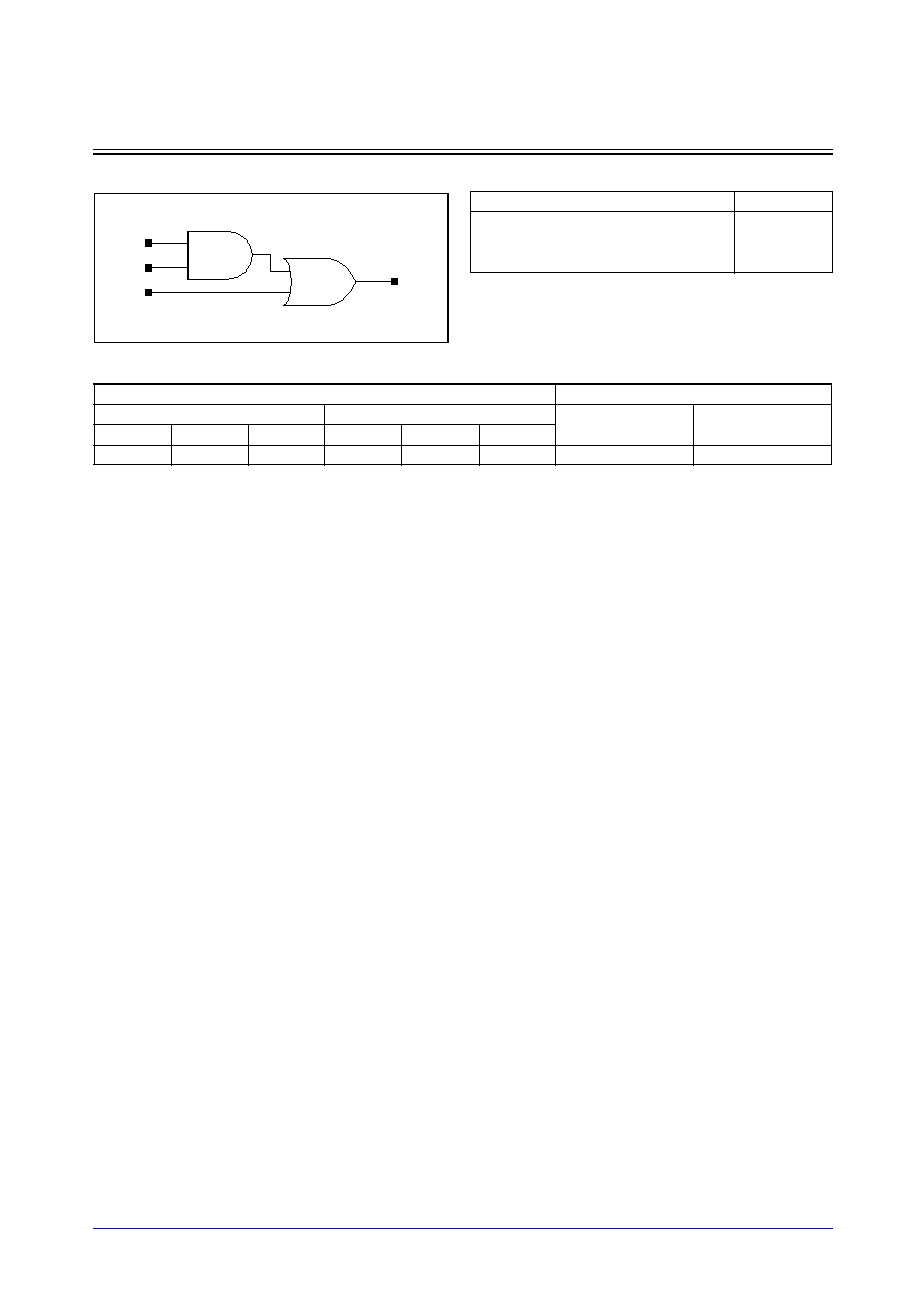
STDL131
3-170
Samsung ASIC
SCG6_LP/SCG6D2_LP
2-AND into 2-OR with 1X/2X Drive
Logic Symbol
Cell Data
Input Load (SL)
Gate Count
SCG6_LP
SCG6D2_LP
SCG6_LP
SCG6D2_LP
A
B
C
A
B
C
0.9
0.9
0.9
1.1
1.1
1.1
1.67
2.00
A
B
Y
C
Truth Table
A
B
C
Y
1
1
x
1
x
x
1
1
Other States
0

Samsung ASIC
3-171
STDL131
SCG6_LP/SCG6D2_LP
2-AND into 2-OR with 1X/2X Drive
Switching Characteristics
(Typical process, 25
∞
C, 1.8V, t
R
/t
F
= 0.19ns, SL: Standard Load)
SCG6_LP
SCG6D2_LP
Path
Parameter
Delay [ns]
SL = 2
Delay Equations [ns]
Group1*
Group2*
Group3*
A to Y
tR
0.096
0.047 + 0.024*SL
0.041 + 0.026*SL
0.038 + 0.026*SL
tF
0.087
0.050 + 0.019*SL
0.057 + 0.017*SL
0.057 + 0.017*SL
tPLH
0.154
0.126 + 0.014*SL
0.131 + 0.013*SL
0.133 + 0.013*SL
tPHL
0.206
0.177 + 0.015*SL
0.188 + 0.012*SL
0.198 + 0.010*SL
B to Y
tR
0.096
0.047 + 0.025*SL
0.041 + 0.026*SL
0.038 + 0.026*SL
tF
0.091
0.054 + 0.018*SL
0.061 + 0.017*SL
0.059 + 0.017*SL
tPLH
0.151
0.123 + 0.014*SL
0.128 + 0.013*SL
0.130 + 0.013*SL
tPHL
0.224
0.195 + 0.015*SL
0.207 + 0.012*SL
0.217 + 0.010*SL
C to Y
tR
0.096
0.050 + 0.023*SL
0.036 + 0.026*SL
0.034 + 0.027*SL
tF
0.091
0.056 + 0.018*SL
0.057 + 0.017*SL
0.061 + 0.017*SL
tPLH
0.158
0.131 + 0.013*SL
0.133 + 0.013*SL
0.135 + 0.013*SL
tPHL
0.262
0.232 + 0.015*SL
0.244 + 0.012*SL
0.255 + 0.010*SL
*Group1 : SL < 4, *Group2 : 4 SL
<
<
=
= 8, *Group3 : 8 < SL
Path
Parameter
Delay [ns]
SL = 2
Delay Equations [ns]
Group1*
Group2*
Group3*
A to Y
tR
0.073
0.049 + 0.012*SL
0.047 + 0.013*SL
0.043 + 0.013*SL
tF
0.075
0.054 + 0.010*SL
0.061 + 0.009*SL
0.066 + 0.008*SL
tPLH
0.159
0.141 + 0.009*SL
0.148 + 0.007*SL
0.155 + 0.006*SL
tPHL
0.211
0.192 + 0.010*SL
0.203 + 0.007*SL
0.219 + 0.005*SL
B to Y
tR
0.074
0.049 + 0.012*SL
0.048 + 0.013*SL
0.042 + 0.013*SL
tF
0.078
0.057 + 0.010*SL
0.063 + 0.009*SL
0.068 + 0.008*SL
tPLH
0.155
0.138 + 0.009*SL
0.145 + 0.007*SL
0.151 + 0.006*SL
tPHL
0.228
0.208 + 0.010*SL
0.219 + 0.007*SL
0.236 + 0.005*SL
C to Y
tR
0.065
0.040 + 0.012*SL
0.040 + 0.013*SL
0.033 + 0.013*SL
tF
0.078
0.058 + 0.010*SL
0.063 + 0.009*SL
0.068 + 0.008*SL
tPLH
0.158
0.142 + 0.008*SL
0.147 + 0.007*SL
0.150 + 0.006*SL
tPHL
0.264
0.245 + 0.010*SL
0.256 + 0.007*SL
0.273 + 0.005*SL
*Group1 : SL < 4, *Group2 : 4 SL
<
<
=
= 12, *Group3 : 12 < SL

STDL131
3-172
Samsung ASIC
SCG7_LP/SCG7D2_LP
2-NAND and (2-AND into 2-NOR) into 2-NAND with 1X/2X Drive
Logic Symbol
Cell Data
Switching Characteristics
(Typical process, 25
∞
C, 1.8V, t
R
/t
F
= 0.19ns, SL: Standard Load)
SCG7_LP
Input Load (SL)
Gate Count
SCG7_LP
SCG7D2_LP
SCG7_LP
SCG7D2_LP
A
B
C
D
E
A
B
C
D
E
0.7
0.7
0.7
0.7
0.7
1.0
1.0
1.1
1.1
1.0
3.00
3.67
C
D
E
A
B
Y
Path
Parameter
Delay [ns]
SL = 2
Delay Equations [ns]
Group1*
Group2*
Group3*
A to Y
tR
0.109
0.060 + 0.025*SL
0.056 + 0.026*SL
0.052 + 0.026*SL
tF
0.110
0.059 + 0.025*SL
0.059 + 0.026*SL
0.055 + 0.026*SL
tPLH
0.166
0.139 + 0.014*SL
0.143 + 0.013*SL
0.144 + 0.012*SL
tPHL
0.191
0.161 + 0.015*SL
0.165 + 0.014*SL
0.167 + 0.014*SL
B to Y
tR
0.109
0.059 + 0.025*SL
0.056 + 0.026*SL
0.052 + 0.026*SL
tF
0.111
0.062 + 0.025*SL
0.057 + 0.026*SL
0.056 + 0.026*SL
tPLH
0.163
0.136 + 0.014*SL
0.140 + 0.013*SL
0.141 + 0.012*SL
tPHL
0.202
0.171 + 0.015*SL
0.176 + 0.014*SL
0.178 + 0.014*SL
C to Y
tR
0.124
0.075 + 0.025*SL
0.071 + 0.026*SL
0.067 + 0.026*SL
tF
0.119
0.068 + 0.026*SL
0.068 + 0.026*SL
0.065 + 0.026*SL
tPLH
0.203
0.175 + 0.014*SL
0.180 + 0.013*SL
0.182 + 0.013*SL
tPHL
0.233
0.200 + 0.017*SL
0.207 + 0.015*SL
0.212 + 0.014*SL
D to Y
tR
0.124
0.075 + 0.025*SL
0.071 + 0.025*SL
0.066 + 0.026*SL
tF
0.120
0.069 + 0.025*SL
0.069 + 0.025*SL
0.065 + 0.026*SL
tPLH
0.201
0.173 + 0.014*SL
0.178 + 0.013*SL
0.180 + 0.013*SL
tPHL
0.247
0.214 + 0.017*SL
0.221 + 0.015*SL
0.227 + 0.014*SL
E to Y
tR
0.123
0.073 + 0.025*SL
0.070 + 0.026*SL
0.065 + 0.026*SL
tF
0.120
0.069 + 0.025*SL
0.069 + 0.025*SL
0.065 + 0.026*SL
tPLH
0.235
0.208 + 0.014*SL
0.211 + 0.013*SL
0.213 + 0.013*SL
tPHL
0.286
0.252 + 0.017*SL
0.259 + 0.015*SL
0.265 + 0.014*SL
*Group1 : SL < 4, *Group2 : 4 SL
<
<
=
= 8, *Group3 : 8 < SL
Truth Table
A
B
C
D
E
Y
1
1
x
x
x
1
x
x
1
1
x
1
x
x
x
x
1
1
Other States
0

Samsung ASIC
3-173
STDL131
SCG7_LP/SCG7D2_LP
2-NAND and (2-AND into 2-NOR) into 2-NAND with 1X/2X Drive
Switching Characteristics
(Typical process, 25
∞
C, 1.8V, t
R
/t
F
= 0.19ns, SL: Standard Load)
SCG7D2_LP
Path
Parameter
Delay [ns]
SL = 2
Delay Equations [ns]
Group1*
Group2*
Group3*
A to Y
tR
0.086
0.061 + 0.012*SL
0.061 + 0.013*SL
0.054 + 0.013*SL
tF
0.085
0.061 + 0.012*SL
0.059 + 0.013*SL
0.054 + 0.013*SL
tPLH
0.163
0.147 + 0.008*SL
0.152 + 0.007*SL
0.157 + 0.006*SL
tPHL
0.183
0.165 + 0.009*SL
0.170 + 0.008*SL
0.175 + 0.007*SL
B to Y
tR
0.086
0.062 + 0.012*SL
0.059 + 0.013*SL
0.054 + 0.013*SL
tF
0.085
0.060 + 0.013*SL
0.060 + 0.013*SL
0.055 + 0.013*SL
tPLH
0.160
0.144 + 0.008*SL
0.149 + 0.007*SL
0.154 + 0.006*SL
tPHL
0.193
0.175 + 0.009*SL
0.180 + 0.008*SL
0.185 + 0.007*SL
C to Y
tR
0.099
0.075 + 0.012*SL
0.074 + 0.012*SL
0.067 + 0.013*SL
tF
0.094
0.066 + 0.014*SL
0.070 + 0.013*SL
0.067 + 0.013*SL
tPLH
0.197
0.181 + 0.008*SL
0.186 + 0.007*SL
0.191 + 0.006*SL
tPHL
0.235
0.216 + 0.010*SL
0.222 + 0.008*SL
0.231 + 0.007*SL
D to Y
tR
0.099
0.075 + 0.012*SL
0.072 + 0.013*SL
0.068 + 0.013*SL
tF
0.096
0.069 + 0.014*SL
0.072 + 0.013*SL
0.068 + 0.013*SL
tPLH
0.193
0.177 + 0.008*SL
0.182 + 0.007*SL
0.187 + 0.006*SL
tPHL
0.249
0.230 + 0.010*SL
0.236 + 0.008*SL
0.245 + 0.007*SL
E to Y
tR
0.099
0.075 + 0.012*SL
0.074 + 0.012*SL
0.066 + 0.013*SL
tF
0.096
0.071 + 0.013*SL
0.069 + 0.013*SL
0.069 + 0.013*SL
tPLH
0.233
0.217 + 0.008*SL
0.221 + 0.007*SL
0.226 + 0.006*SL
tPHL
0.286
0.267 + 0.010*SL
0.273 + 0.008*SL
0.282 + 0.007*SL
*Group1 : SL < 4, *Group2 : 4 SL
<
<
=
= 12, *Group3 : 12 < SL
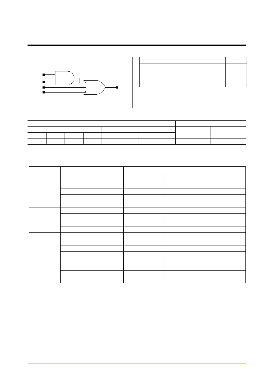
STDL131
3-174
Samsung ASIC
SCG8_LP/SCG8D2_LP
2-AND into 3-OR with 1X/2X Drive
Logic Symbol
Cell Data
Switching Characteristics
(Typical process, 25
∞
C, 1.8V, t
R
/t
F
= 0.19ns, SL: Standard Load)
SCG8_LP
Input Load (SL)
Gate Count
SCG8_LP
SCG8D2_LP
SCG8_LP
SCG8D2_LP
A
B
C
D
A
B
C
D
0.9
0.9
0.9
0.9
1.1
1.1
1.1
1.1
2.00
2.67
A
B
Y
C
D
Path
Parameter
Delay [ns]
SL = 2
Delay Equations [ns]
Group1*
Group2*
Group3*
A to Y
tR
0.101
0.052 + 0.024*SL
0.047 + 0.026*SL
0.043 + 0.026*SL
tF
0.112
0.071 + 0.020*SL
0.082 + 0.018*SL
0.090 + 0.017*SL
tPLH
0.169
0.140 + 0.014*SL
0.146 + 0.013*SL
0.148 + 0.013*SL
tPHL
0.254
0.220 + 0.017*SL
0.234 + 0.014*SL
0.251 + 0.011*SL
B to Y
tR
0.101
0.052 + 0.025*SL
0.048 + 0.026*SL
0.043 + 0.026*SL
tF
0.116
0.077 + 0.020*SL
0.086 + 0.017*SL
0.092 + 0.017*SL
tPLH
0.165
0.137 + 0.014*SL
0.142 + 0.013*SL
0.144 + 0.013*SL
tPHL
0.279
0.244 + 0.017*SL
0.259 + 0.014*SL
0.275 + 0.012*SL
C to Y
tR
0.097
0.047 + 0.025*SL
0.042 + 0.026*SL
0.039 + 0.026*SL
tF
0.117
0.077 + 0.020*SL
0.086 + 0.017*SL
0.093 + 0.017*SL
tPLH
0.179
0.152 + 0.014*SL
0.156 + 0.013*SL
0.157 + 0.013*SL
tPHL
0.358
0.323 + 0.017*SL
0.338 + 0.014*SL
0.355 + 0.012*SL
D to Y
tR
0.101
0.051 + 0.025*SL
0.047 + 0.026*SL
0.043 + 0.026*SL
tF
0.116
0.078 + 0.019*SL
0.085 + 0.018*SL
0.091 + 0.017*SL
tPLH
0.188
0.160 + 0.014*SL
0.164 + 0.013*SL
0.166 + 0.013*SL
tPHL
0.375
0.340 + 0.017*SL
0.355 + 0.014*SL
0.371 + 0.011*SL
*Group1 : SL < 4, *Group2 : 4 SL
<
<
=
= 8, *Group3 : 8 < SL
Truth Table
A
B
C
D
Y
1
1
x
x
1
x
x
1
x
1
x
x
x
1
1
Other States
0
Samsung ASIC
3-175
STDL131
SCG8_LP/SCG8D2_LP
2-AND into 3-OR with 1X/2X Drive
Switching Characteristics
(Typical process, 25
∞
C, 1.8V, t
R
/t
F
= 0.19ns, SL: Standard Load)
SCG8D2_LP
Path
Parameter
Delay [ns]
SL = 2
Delay Equations [ns]
Group1*
Group2*
Group3*
A to Y
tR
0.077
0.053 + 0.012*SL
0.052 + 0.012*SL
0.047 + 0.013*SL
tF
0.101
0.077 + 0.012*SL
0.087 + 0.009*SL
0.098 + 0.009*SL
tPLH
0.170
0.152 + 0.009*SL
0.159 + 0.007*SL
0.167 + 0.006*SL
tPHL
0.272
0.249 + 0.011*SL
0.262 + 0.008*SL
0.286 + 0.006*SL
B to Y
tR
0.077
0.051 + 0.013*SL
0.052 + 0.012*SL
0.047 + 0.013*SL
tF
0.104
0.081 + 0.012*SL
0.089 + 0.010*SL
0.104 + 0.008*SL
tPLH
0.165
0.148 + 0.009*SL
0.155 + 0.007*SL
0.163 + 0.006*SL
tPHL
0.297
0.274 + 0.012*SL
0.287 + 0.008*SL
0.311 + 0.006*SL
C to Y
tR
0.071
0.048 + 0.012*SL
0.045 + 0.012*SL
0.038 + 0.013*SL
tF
0.105
0.080 + 0.012*SL
0.090 + 0.010*SL
0.105 + 0.008*SL
tPLH
0.176
0.160 + 0.008*SL
0.165 + 0.007*SL
0.169 + 0.006*SL
tPHL
0.381
0.358 + 0.012*SL
0.371 + 0.008*SL
0.396 + 0.006*SL
D to Y
tR
0.074
0.050 + 0.012*SL
0.048 + 0.012*SL
0.041 + 0.013*SL
tF
0.105
0.080 + 0.012*SL
0.091 + 0.010*SL
0.104 + 0.008*SL
tPLH
0.184
0.167 + 0.008*SL
0.173 + 0.007*SL
0.178 + 0.006*SL
tPHL
0.398
0.375 + 0.012*SL
0.388 + 0.008*SL
0.412 + 0.006*SL
*Group1 : SL < 4, *Group2 : 4 SL
<
<
=
= 12, *Group3 : 12 < SL

STDL131
3-176
Samsung ASIC
SCG9_LP/SCG9D2_LP
2-OR into 2-AND with 1X/2X Drive
Logic Symbol
Cell Data
Input Load (SL)
Gate Count
SCG9_LP
SCG9D2_LP
SCG9_LP
SCG9D2_LP
A
B
C
A
B
C
0.8
0.8
1.0
1.0
1.0
1.1
1.67
2.33
Y
C
A
B
Truth Table
A
B
C
Y
0
0
x
0
x
x
0
0
Other States
1

Samsung ASIC
3-177
STDL131
SCG9_LP/SCG9D2_LP
2-OR into 2-AND with 1X/2X Drive
Switching Characteristics
(Typical process, 25
∞
C, 1.8V, t
R
/t
F
= 0.19ns, SL: Standard Load)
SCG9_LP
SCG9D2_LP
Path
Parameter
Delay [ns]
SL = 2
Delay Equations [ns]
Group1*
Group2*
Group3*
A to Y
tR
0.097
0.047 + 0.025*SL
0.044 + 0.026*SL
0.039 + 0.026*SL
tF
0.091
0.056 + 0.018*SL
0.059 + 0.017*SL
0.059 + 0.017*SL
tPLH
0.160
0.132 + 0.014*SL
0.137 + 0.013*SL
0.139 + 0.013*SL
tPHL
0.214
0.185 + 0.014*SL
0.196 + 0.012*SL
0.206 + 0.010*SL
B to Y
tR
0.101
0.052 + 0.024*SL
0.048 + 0.026*SL
0.041 + 0.026*SL
tF
0.089
0.052 + 0.018*SL
0.059 + 0.017*SL
0.058 + 0.017*SL
tPLH
0.178
0.149 + 0.014*SL
0.155 + 0.013*SL
0.157 + 0.013*SL
tPHL
0.232
0.203 + 0.015*SL
0.215 + 0.012*SL
0.225 + 0.010*SL
C to Y
tR
0.104
0.057 + 0.023*SL
0.048 + 0.026*SL
0.042 + 0.026*SL
tF
0.083
0.048 + 0.018*SL
0.051 + 0.017*SL
0.051 + 0.017*SL
tPLH
0.170
0.141 + 0.014*SL
0.147 + 0.013*SL
0.149 + 0.013*SL
tPHL
0.180
0.153 + 0.014*SL
0.163 + 0.011*SL
0.172 + 0.010*SL
*Group1 : SL < 4, *Group2 : 4 SL
<
<
=
= 8, *Group3 : 8 < SL
Path
Parameter
Delay [ns]
SL = 2
Delay Equations [ns]
Group1*
Group2*
Group3*
A to Y
tR
0.077
0.054 + 0.012*SL
0.052 + 0.012*SL
0.046 + 0.013*SL
tF
0.080
0.059 + 0.010*SL
0.066 + 0.008*SL
0.070 + 0.008*SL
tPLH
0.169
0.151 + 0.009*SL
0.158 + 0.007*SL
0.165 + 0.006*SL
tPHL
0.226
0.207 + 0.009*SL
0.217 + 0.007*SL
0.234 + 0.005*SL
B to Y
tR
0.079
0.055 + 0.012*SL
0.054 + 0.012*SL
0.049 + 0.013*SL
tF
0.079
0.059 + 0.010*SL
0.065 + 0.009*SL
0.071 + 0.008*SL
tPLH
0.187
0.169 + 0.009*SL
0.176 + 0.007*SL
0.184 + 0.006*SL
tPHL
0.244
0.225 + 0.010*SL
0.236 + 0.007*SL
0.253 + 0.005*SL
C to Y
tR
0.079
0.052 + 0.013*SL
0.056 + 0.012*SL
0.050 + 0.013*SL
tF
0.064
0.044 + 0.010*SL
0.051 + 0.008*SL
0.054 + 0.008*SL
tPLH
0.184
0.167 + 0.009*SL
0.174 + 0.007*SL
0.182 + 0.006*SL
tPHL
0.176
0.160 + 0.008*SL
0.167 + 0.006*SL
0.182 + 0.005*SL
*Group1 : SL < 4, *Group2 : 4 SL
<
<
=
= 12, *Group3 : 12 < SL

STDL131
3-178
Samsung ASIC
SCG10_LP/SCG10D2_LP
Two 2-ORs into 2-AND with 1X/2X Drive
Logic Symbol
Cell Data
Input Load (SL)
Gate Count
SCG10_LP
SCG10D2_LP
SCG10_LP
SCG10D2_LP
A
B
C
D
A
B
C
D
0.8
0.8
0.8
0.8
1.1
1.1
1.0
1.1
2.33
2.67
C
D
Y
A
B
Truth Table
A
B
C
D
Y
0
0
x
x
0
x
x
0
0
0
Other States
1

Samsung ASIC
3-179
STDL131
SCG10_LP/SCG10D2_LP
Two 2-ORs into 2-AND with 1X/2X Drive
Switching Characteristics
(Typical process, 25
∞
C, 1.8V, t
R
/t
F
= 0.19ns, SL: Standard Load)
SCG10_LP
SCG10D2_LP
Path
Parameter
Delay [ns]
SL = 2
Delay Equations [ns]
Group1*
Group2*
Group3*
A to Y
tR
0.110
0.061 + 0.025*SL
0.058 + 0.025*SL
0.053 + 0.026*SL
tF
0.109
0.066 + 0.021*SL
0.079 + 0.018*SL
0.088 + 0.017*SL
tPLH
0.223
0.192 + 0.016*SL
0.201 + 0.013*SL
0.206 + 0.013*SL
tPHL
0.237
0.200 + 0.018*SL
0.218 + 0.014*SL
0.237 + 0.011*SL
B to Y
tR
0.113
0.064 + 0.025*SL
0.061 + 0.025*SL
0.056 + 0.026*SL
tF
0.109
0.066 + 0.022*SL
0.082 + 0.018*SL
0.090 + 0.017*SL
tPLH
0.246
0.214 + 0.016*SL
0.224 + 0.013*SL
0.229 + 0.013*SL
tPHL
0.256
0.219 + 0.018*SL
0.236 + 0.014*SL
0.256 + 0.011*SL
C to Y
tR
0.111
0.062 + 0.025*SL
0.061 + 0.025*SL
0.052 + 0.026*SL
tF
0.114
0.071 + 0.021*SL
0.086 + 0.018*SL
0.094 + 0.017*SL
tPLH
0.232
0.201 + 0.016*SL
0.210 + 0.013*SL
0.215 + 0.013*SL
tPHL
0.266
0.229 + 0.019*SL
0.247 + 0.014*SL
0.267 + 0.012*SL
D to Y
tR
0.115
0.066 + 0.024*SL
0.063 + 0.025*SL
0.055 + 0.026*SL
tF
0.113
0.071 + 0.021*SL
0.084 + 0.018*SL
0.093 + 0.017*SL
tPLH
0.255
0.223 + 0.016*SL
0.233 + 0.013*SL
0.239 + 0.013*SL
tPHL
0.285
0.248 + 0.019*SL
0.266 + 0.014*SL
0.286 + 0.012*SL
*Group1 : SL < 4, *Group2 : 4 SL
<
<
=
= 8, *Group3 : 8 < SL
Path
Parameter
Delay [ns]
SL = 2
Delay Equations [ns]
Group1*
Group2*
Group3*
A to Y
tR
0.083
0.058 + 0.012*SL
0.058 + 0.012*SL
0.054 + 0.013*SL
tF
0.087
0.060 + 0.013*SL
0.074 + 0.010*SL
0.089 + 0.008*SL
tPLH
0.208
0.188 + 0.010*SL
0.198 + 0.007*SL
0.208 + 0.006*SL
tPHL
0.228
0.206 + 0.011*SL
0.218 + 0.008*SL
0.244 + 0.006*SL
B to Y
tR
0.086
0.061 + 0.012*SL
0.060 + 0.012*SL
0.056 + 0.013*SL
tF
0.086
0.061 + 0.013*SL
0.072 + 0.010*SL
0.089 + 0.009*SL
tPLH
0.228
0.209 + 0.010*SL
0.218 + 0.007*SL
0.229 + 0.006*SL
tPHL
0.247
0.224 + 0.011*SL
0.236 + 0.008*SL
0.263 + 0.006*SL
C to Y
tR
0.084
0.059 + 0.012*SL
0.059 + 0.012*SL
0.053 + 0.013*SL
tF
0.091
0.065 + 0.013*SL
0.077 + 0.010*SL
0.096 + 0.008*SL
tPLH
0.216
0.197 + 0.010*SL
0.206 + 0.007*SL
0.217 + 0.006*SL
tPHL
0.258
0.234 + 0.012*SL
0.247 + 0.008*SL
0.275 + 0.006*SL
D to Y
tR
0.086
0.061 + 0.013*SL
0.062 + 0.012*SL
0.055 + 0.013*SL
tF
0.091
0.063 + 0.014*SL
0.080 + 0.010*SL
0.095 + 0.008*SL
tPLH
0.237
0.217 + 0.010*SL
0.227 + 0.007*SL
0.238 + 0.006*SL
tPHL
0.277
0.253 + 0.012*SL
0.266 + 0.008*SL
0.293 + 0.006*SL
*Group1 : SL < 4, *Group2 : 4 SL
<
<
=
= 12, *Group3 : 12 < SL
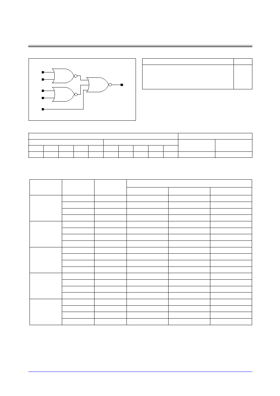
STDL131
3-180
Samsung ASIC
SCG11_LP/SCG11D2_LP
Two 2-NORs into 3-NOR with 1X/2X Drive
Logic Symbol
Cell Data
Switching Characteristics
(Typical process, 25
∞
C, 1.8V, t
R
/t
F
= 0.19ns, SL: Standard Load)
SCG11_LP
Input Load (SL)
Gate Count
SCG11_LP
SCG11D2_LP
SCG11_LP
SCG11D2_LP
A
B
C
D
E
A
B
C
D
E
0.9
0.9
0.9
0.9
1.0
1.1
1.1
1.1
1.1
1.9
3.00
4.00
C
D
Y
A
B
E
Path
Parameter
Delay [ns]
SL = 2
Delay Equations [ns]
Group1*
Group2*
Group3*
A to Y
tR
0.305
0.140 + 0.082*SL
0.144 + 0.081*SL
0.147 + 0.081*SL
tF
0.120
0.069 + 0.026*SL
0.069 + 0.026*SL
0.066 + 0.026*SL
tPLH
0.197
0.116 + 0.040*SL
0.118 + 0.040*SL
0.120 + 0.040*SL
tPHL
0.244
0.207 + 0.019*SL
0.217 + 0.016*SL
0.225 + 0.015*SL
B to Y
tR
0.306
0.141 + 0.082*SL
0.144 + 0.082*SL
0.148 + 0.081*SL
tF
0.120
0.069 + 0.026*SL
0.070 + 0.025*SL
0.065 + 0.026*SL
tPLH
0.207
0.126 + 0.040*SL
0.128 + 0.040*SL
0.130 + 0.040*SL
tPHL
0.263
0.225 + 0.019*SL
0.236 + 0.016*SL
0.244 + 0.015*SL
C to Y
tR
0.312
0.151 + 0.080*SL
0.150 + 0.081*SL
0.149 + 0.081*SL
tF
0.140
0.089 + 0.025*SL
0.087 + 0.026*SL
0.085 + 0.026*SL
tPLH
0.248
0.168 + 0.040*SL
0.169 + 0.040*SL
0.170 + 0.040*SL
tPHL
0.267
0.232 + 0.018*SL
0.239 + 0.016*SL
0.246 + 0.015*SL
D to Y
tR
0.313
0.152 + 0.080*SL
0.150 + 0.081*SL
0.149 + 0.081*SL
tF
0.138
0.086 + 0.026*SL
0.089 + 0.026*SL
0.085 + 0.026*SL
tPLH
0.259
0.179 + 0.040*SL
0.180 + 0.040*SL
0.181 + 0.040*SL
tPHL
0.285
0.250 + 0.018*SL
0.258 + 0.016*SL
0.264 + 0.015*SL
E to Y
tR
0.314
0.154 + 0.080*SL
0.150 + 0.081*SL
0.149 + 0.081*SL
tF
0.147
0.098 + 0.025*SL
0.094 + 0.025*SL
0.087 + 0.026*SL
tPLH
0.246
0.166 + 0.040*SL
0.166 + 0.040*SL
0.167 + 0.040*SL
tPHL
0.129
0.096 + 0.016*SL
0.099 + 0.016*SL
0.103 + 0.015*SL
*Group1 : SL < 4, *Group2 : 4 SL
<
<
=
= 8, *Group3 : 8 < SL
Truth Table
A
B
C
D
E
Y
0
0
x
x
x
0
x
x
0
0
x
0
x
x
x
x
1
0
Other States
1

Samsung ASIC
3-181
STDL131
SCG11_LP/SCG11D2_LP
Two 2-NORs into 3-NOR with 1X/2X Drive
Switching Characteristics
(Typical process, 25
∞
C, 1.8V, t
R
/t
F
= 0.19ns, SL: Standard Load)
SCG11D2_LP
Path
Parameter
Delay [ns]
SL = 2
Delay Equations [ns]
Group1*
Group2*
Group3*
A to Y
tR
0.229
0.148 + 0.041*SL
0.147 + 0.041*SL
0.152 + 0.040*SL
tF
0.102
0.075 + 0.013*SL
0.078 + 0.013*SL
0.076 + 0.013*SL
tPLH
0.183
0.142 + 0.020*SL
0.143 + 0.020*SL
0.145 + 0.020*SL
tPHL
0.242
0.220 + 0.011*SL
0.229 + 0.009*SL
0.242 + 0.008*SL
B to Y
tR
0.230
0.148 + 0.041*SL
0.148 + 0.041*SL
0.152 + 0.040*SL
tF
0.101
0.074 + 0.014*SL
0.076 + 0.013*SL
0.076 + 0.013*SL
tPLH
0.195
0.155 + 0.020*SL
0.155 + 0.020*SL
0.157 + 0.020*SL
tPHL
0.262
0.240 + 0.011*SL
0.249 + 0.009*SL
0.262 + 0.008*SL
C to Y
tR
0.238
0.159 + 0.040*SL
0.157 + 0.040*SL
0.155 + 0.040*SL
tF
0.120
0.093 + 0.013*SL
0.096 + 0.013*SL
0.093 + 0.013*SL
tPLH
0.234
0.194 + 0.020*SL
0.195 + 0.020*SL
0.196 + 0.020*SL
tPHL
0.263
0.243 + 0.010*SL
0.249 + 0.008*SL
0.259 + 0.008*SL
D to Y
tR
0.238
0.159 + 0.040*SL
0.157 + 0.040*SL
0.155 + 0.040*SL
tF
0.120
0.094 + 0.013*SL
0.095 + 0.013*SL
0.093 + 0.013*SL
tPLH
0.247
0.207 + 0.020*SL
0.207 + 0.020*SL
0.209 + 0.020*SL
tPHL
0.282
0.262 + 0.010*SL
0.268 + 0.008*SL
0.278 + 0.008*SL
E to Y
tR
0.240
0.161 + 0.039*SL
0.158 + 0.040*SL
0.155 + 0.040*SL
tF
0.125
0.101 + 0.012*SL
0.099 + 0.012*SL
0.092 + 0.013*SL
tPLH
0.210
0.170 + 0.020*SL
0.171 + 0.020*SL
0.172 + 0.020*SL
tPHL
0.114
0.097 + 0.008*SL
0.099 + 0.008*SL
0.103 + 0.008*SL
*Group1 : SL < 4, *Group2 : 4 SL
<
<
=
= 12, *Group3 : 12 < SL
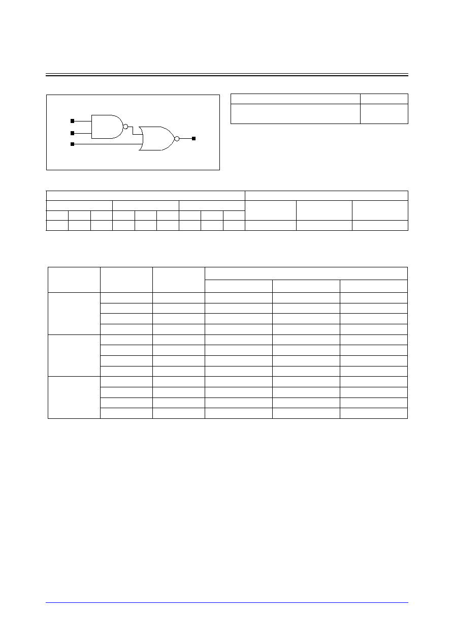
STDL131
3-182
Samsung ASIC
SCG12_LP/SCG12D2_LP/SCG12D4_LP
2-NAND into 2-NOR with 1X/2X/4X Drive
Logic Symbol
Cell Data
Switching Characteristics
(Typical process, 25
∞
C, 1.8V, t
R
/t
F
= 0.19ns, SL: Standard Load)
SCG12_LP
Input Load (SL)
Gate Count
SCG12_LP
SCG12D2_LP
SCG12D4_LP
SCG12_LP
SCG12D2_LP
SCG12D4_LP
A
B
C
A
B
C
A
B
C
0.8
0.8
1.2
0.8
0.9
2.3
0.7
0.7
0.9
1.67
2.33
4.00
A
B
Y
C
Path
Parameter
Delay [ns]
SL = 2
Delay Equations [ns]
Group1*
Group2*
Group3*
A to Y
tR
0.195
0.089 + 0.053*SL
0.086 + 0.054*SL
0.084 + 0.054*SL
tF
0.073
0.041 + 0.016*SL
0.043 + 0.015*SL
0.040 + 0.016*SL
tPLH
0.184
0.131 + 0.027*SL
0.132 + 0.026*SL
0.134 + 0.026*SL
tPHL
0.172
0.150 + 0.011*SL
0.156 + 0.009*SL
0.160 + 0.009*SL
B to Y
tR
0.195
0.089 + 0.053*SL
0.085 + 0.054*SL
0.084 + 0.054*SL
tF
0.075
0.045 + 0.015*SL
0.044 + 0.015*SL
0.041 + 0.016*SL
tPLH
0.183
0.129 + 0.027*SL
0.131 + 0.026*SL
0.133 + 0.026*SL
tPHL
0.186
0.164 + 0.011*SL
0.170 + 0.010*SL
0.175 + 0.009*SL
C to Y
tR
0.199
0.095 + 0.052*SL
0.089 + 0.053*SL
0.085 + 0.054*SL
tF
0.097
0.069 + 0.014*SL
0.069 + 0.014*SL
0.059 + 0.015*SL
tPLH
0.164
0.111 + 0.026*SL
0.112 + 0.026*SL
0.112 + 0.026*SL
tPHL
0.085
0.062 + 0.012*SL
0.072 + 0.009*SL
0.074 + 0.009*SL
*Group1 : SL < 4, *Group2 : 4 SL
<
<
=
= 8, *Group3 : 8 < SL
Truth Table
A
B
C
Y
1
1
0
1
Other States
0

Samsung ASIC
3-183
STDL131
SCG12_LP/SCG12D2_LP/SCG12D4_LP
2-NAND into 2-NOR with 1X/2X/4X Drive
Switching Characteristics
(Typical process, 25
∞
C, 1.8V, t
R
/t
F
= 0.19ns, SL: Standard Load)
SCG12D2_LP
SCG12D4_LP
Path
Parameter
Delay [ns]
SL = 2
Delay Equations [ns]
Group1*
Group2*
Group3*
A to Y
tR
0.137
0.085 + 0.026*SL
0.083 + 0.027*SL
0.078 + 0.027*SL
tF
0.065
0.048 + 0.008*SL
0.051 + 0.008*SL
0.050 + 0.008*SL
tPLH
0.176
0.148 + 0.014*SL
0.150 + 0.013*SL
0.152 + 0.013*SL
tPHL
0.187
0.172 + 0.007*SL
0.180 + 0.006*SL
0.190 + 0.005*SL
B to Y
tR
0.137
0.085 + 0.026*SL
0.082 + 0.027*SL
0.077 + 0.027*SL
tF
0.067
0.051 + 0.008*SL
0.052 + 0.008*SL
0.052 + 0.008*SL
tPLH
0.173
0.145 + 0.014*SL
0.148 + 0.013*SL
0.149 + 0.013*SL
tPHL
0.201
0.186 + 0.007*SL
0.193 + 0.006*SL
0.204 + 0.005*SL
C to Y
tR
0.139
0.088 + 0.025*SL
0.084 + 0.026*SL
0.078 + 0.027*SL
tF
0.081
0.067 + 0.007*SL
0.067 + 0.007*SL
0.062 + 0.007*SL
tPLH
0.134
0.107 + 0.014*SL
0.109 + 0.013*SL
0.110 + 0.013*SL
tPHL
0.070
0.055 + 0.007*SL
0.063 + 0.005*SL
0.071 + 0.004*SL
*Group1 : SL < 4, *Group2 : 4 SL
<
<
=
= 12, *Group3 : 12 < SL
Path
Parameter
Delay [ns]
SL = 2
Delay Equations [ns]
Group1*
Group2*
Group3*
A to Y
tR
0.061
0.050 + 0.006*SL
0.048 + 0.006*SL
0.040 + 0.006*SL
tF
0.055
0.045 + 0.005*SL
0.048 + 0.004*SL
0.047 + 0.004*SL
tPLH
0.334
0.324 + 0.005*SL
0.329 + 0.004*SL
0.336 + 0.003*SL
tPHL
0.310
0.301 + 0.005*SL
0.307 + 0.003*SL
0.321 + 0.003*SL
B to Y
tR
0.061
0.047 + 0.007*SL
0.050 + 0.006*SL
0.042 + 0.006*SL
tF
0.055
0.046 + 0.005*SL
0.048 + 0.004*SL
0.047 + 0.004*SL
tPLH
0.332
0.322 + 0.005*SL
0.327 + 0.004*SL
0.334 + 0.003*SL
tPHL
0.321
0.312 + 0.005*SL
0.318 + 0.003*SL
0.332 + 0.003*SL
C to Y
tR
0.062
0.051 + 0.005*SL
0.048 + 0.006*SL
0.040 + 0.007*SL
tF
0.055
0.047 + 0.004*SL
0.046 + 0.004*SL
0.049 + 0.004*SL
tPLH
0.299
0.289 + 0.005*SL
0.294 + 0.004*SL
0.301 + 0.003*SL
tPHL
0.231
0.222 + 0.005*SL
0.228 + 0.003*SL
0.242 + 0.003*SL
*Group1 : SL < 4, *Group2 : 4 SL
<
<
=
= 20, *Group3 : 20 < SL

STDL131
3-184
Samsung ASIC
SCG13_LP/SCG13D2_LP
2-NOR into 2-NAND with 1X/2X Drive
Logic Symbol
Cell Data
Input Load (SL)
Gate Count
SCG13_LP
SCG13D2_LP
SCG13_LP
SCG13D2_LP
A
B
C
A
B
C
0.8
0.8
1.2
1.0
1.0
2.3
2.00
2.67
Y
A
B
C
Truth Table
A
B
C
Y
0
0
1
0
Other States
1

Samsung ASIC
3-185
STDL131
SCG13_LP/SCG13D2_LP
2-NOR into 2-NAND with 1X/2X Drive
Switching Characteristics
(Typical process, 25
∞
C, 1.8V, t
R
/t
F
= 0.19ns, SL: Standard Load)
SCG13_LP
SCG13D2_LP
Path
Parameter
Delay [ns]
SL = 2
Delay Equations [ns]
Group1*
Group2*
Group3*
A to Y
tR
0.110
0.062 + 0.024*SL
0.056 + 0.026*SL
0.052 + 0.026*SL
tF
0.123
0.073 + 0.025*SL
0.072 + 0.025*SL
0.070 + 0.026*SL
tPLH
0.177
0.151 + 0.013*SL
0.154 + 0.013*SL
0.155 + 0.012*SL
tPHL
0.221
0.187 + 0.017*SL
0.195 + 0.015*SL
0.200 + 0.014*SL
B to Y
tR
0.112
0.063 + 0.025*SL
0.059 + 0.025*SL
0.054 + 0.026*SL
tF
0.123
0.072 + 0.025*SL
0.073 + 0.025*SL
0.070 + 0.026*SL
tPLH
0.200
0.173 + 0.013*SL
0.176 + 0.013*SL
0.178 + 0.012*SL
tPHL
0.241
0.207 + 0.017*SL
0.215 + 0.015*SL
0.221 + 0.014*SL
C to Y
tR
0.130
0.086 + 0.022*SL
0.077 + 0.024*SL
0.068 + 0.026*SL
tF
0.117
0.068 + 0.024*SL
0.065 + 0.025*SL
0.059 + 0.026*SL
tPLH
0.112
0.086 + 0.013*SL
0.089 + 0.012*SL
0.089 + 0.012*SL
tPHL
0.095
0.063 + 0.016*SL
0.070 + 0.014*SL
0.072 + 0.014*SL
*Group1 : SL < 4, *Group2 : 4 SL
<
<
=
= 8, *Group3 : 8 < SL
Path
Parameter
Delay [ns]
SL = 2
Delay Equations [ns]
Group1*
Group2*
Group3*
A to Y
tR
0.089
0.066 + 0.011*SL
0.062 + 0.012*SL
0.057 + 0.013*SL
tF
0.103
0.076 + 0.013*SL
0.080 + 0.012*SL
0.077 + 0.013*SL
tPLH
0.181
0.166 + 0.008*SL
0.170 + 0.007*SL
0.173 + 0.006*SL
tPHL
0.225
0.206 + 0.010*SL
0.212 + 0.008*SL
0.223 + 0.007*SL
B to Y
tR
0.092
0.070 + 0.011*SL
0.064 + 0.012*SL
0.059 + 0.013*SL
tF
0.103
0.078 + 0.012*SL
0.077 + 0.013*SL
0.076 + 0.013*SL
tPLH
0.203
0.187 + 0.008*SL
0.192 + 0.007*SL
0.196 + 0.006*SL
tPHL
0.245
0.226 + 0.010*SL
0.232 + 0.008*SL
0.243 + 0.007*SL
C to Y
tR
0.108
0.087 + 0.010*SL
0.082 + 0.012*SL
0.069 + 0.013*SL
tF
0.091
0.066 + 0.012*SL
0.066 + 0.012*SL
0.061 + 0.013*SL
tPLH
0.096
0.081 + 0.008*SL
0.086 + 0.006*SL
0.088 + 0.006*SL
tPHL
0.077
0.059 + 0.009*SL
0.065 + 0.008*SL
0.070 + 0.007*SL
*Group1 : SL < 4, *Group2 : 4 SL
<
<
=
= 12, *Group3 : 12 < SL
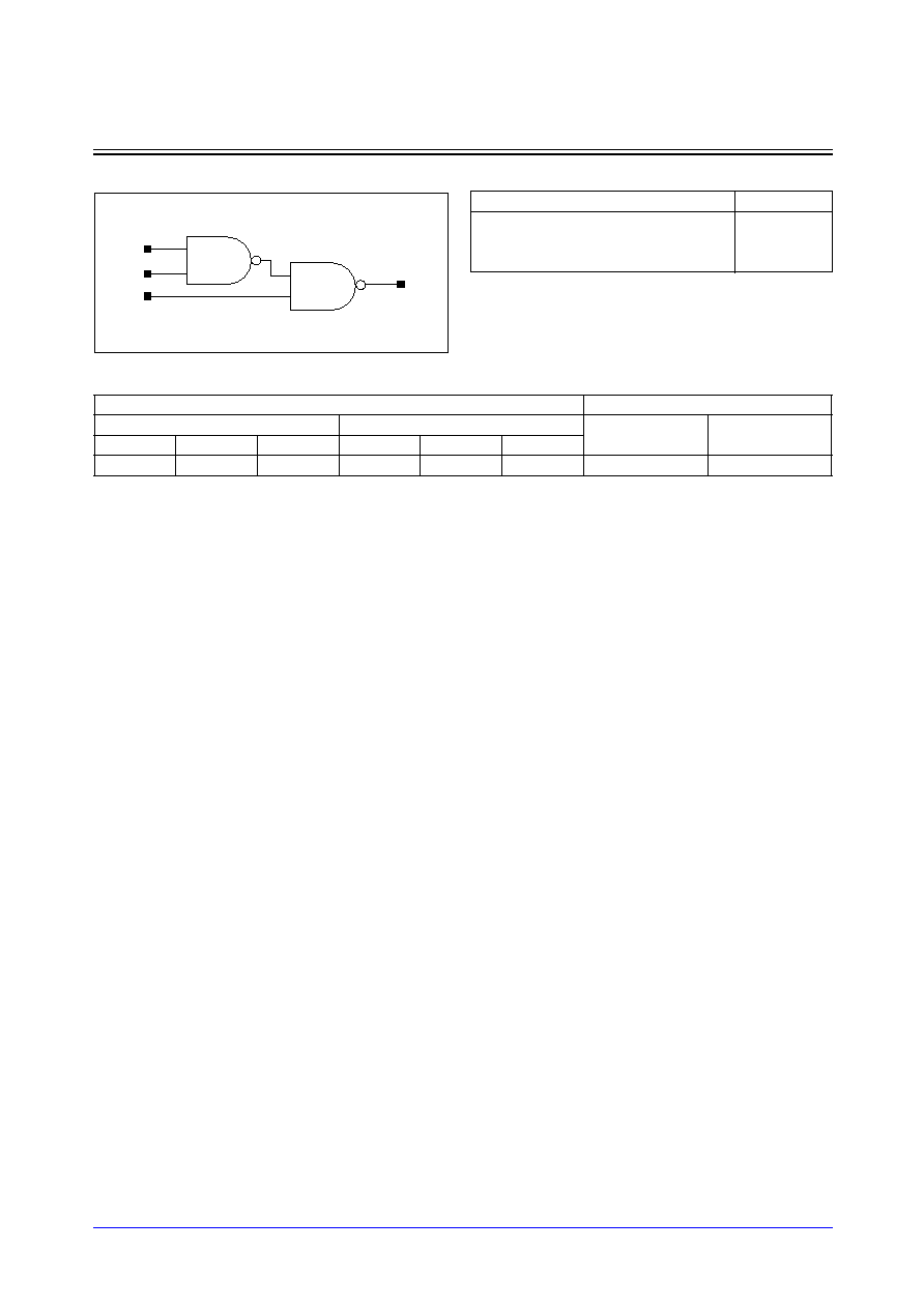
STDL131
3-186
Samsung ASIC
SCG14_LP/SCG14D2_LP
2-NAND into 2-NAND with 1X/2X Drive
Logic Symbol
Cell Data
Input Load (SL)
Gate Count
SCG14_LP
SCG14D2_LP
SCG14_LP
SCG14D2_LP
A
B
C
A
B
C
0.7
0.7
1.2
1.0
1.0
2.3
1.67
2.33
A
B
Y
C
Truth Table
A
B
C
Y
0
x
1
0
x
0
1
0
Other States
1
Samsung ASIC
3-187
STDL131
SCG14_LP/SCG14D2_LP
2-NAND into 2-NAND with 1X/2X Drive
Switching Characteristics
(Typical process, 25
∞
C, 1.8V, t
R
/t
F
= 0.19ns, SL: Standard Load)
SCG14_LP
SCG14D2_LP
Path
Parameter
Delay [ns]
SL = 2
Delay Equations [ns]
Group1*
Group2*
Group3*
A to Y
tR
0.111
0.062 + 0.025*SL
0.058 + 0.026*SL
0.053 + 0.026*SL
tF
0.108
0.058 + 0.025*SL
0.055 + 0.026*SL
0.050 + 0.027*SL
tPLH
0.177
0.148 + 0.014*SL
0.153 + 0.013*SL
0.156 + 0.013*SL
tPHL
0.184
0.154 + 0.015*SL
0.158 + 0.014*SL
0.159 + 0.014*SL
B to Y
tR
0.111
0.061 + 0.025*SL
0.059 + 0.025*SL
0.052 + 0.026*SL
tF
0.110
0.060 + 0.025*SL
0.057 + 0.026*SL
0.051 + 0.027*SL
tPLH
0.172
0.144 + 0.014*SL
0.149 + 0.013*SL
0.151 + 0.013*SL
tPHL
0.193
0.162 + 0.015*SL
0.166 + 0.014*SL
0.168 + 0.014*SL
C to Y
tR
0.128
0.084 + 0.022*SL
0.074 + 0.025*SL
0.064 + 0.026*SL
tF
0.114
0.065 + 0.024*SL
0.061 + 0.025*SL
0.055 + 0.026*SL
tPLH
0.111
0.084 + 0.013*SL
0.088 + 0.013*SL
0.088 + 0.013*SL
tPHL
0.093
0.061 + 0.016*SL
0.068 + 0.014*SL
0.070 + 0.014*SL
*Group1 : SL < 4, *Group2 : 4 SL
<
<
=
= 8, *Group3 : 8 < SL
Path
Parameter
Delay [ns]
SL = 2
Delay Equations [ns]
Group1*
Group2*
Group3*
A to Y
tR
0.087
0.062 + 0.013*SL
0.064 + 0.012*SL
0.055 + 0.013*SL
tF
0.086
0.061 + 0.013*SL
0.060 + 0.013*SL
0.054 + 0.013*SL
tPLH
0.166
0.150 + 0.008*SL
0.155 + 0.007*SL
0.161 + 0.006*SL
tPHL
0.183
0.166 + 0.009*SL
0.170 + 0.008*SL
0.175 + 0.007*SL
B to Y
tR
0.088
0.064 + 0.012*SL
0.062 + 0.012*SL
0.055 + 0.013*SL
tF
0.086
0.061 + 0.013*SL
0.060 + 0.013*SL
0.055 + 0.013*SL
tPLH
0.163
0.147 + 0.008*SL
0.152 + 0.007*SL
0.157 + 0.006*SL
tPHL
0.193
0.175 + 0.009*SL
0.180 + 0.008*SL
0.185 + 0.007*SL
C to Y
tR
0.105
0.084 + 0.010*SL
0.079 + 0.012*SL
0.066 + 0.013*SL
tF
0.088
0.063 + 0.013*SL
0.063 + 0.013*SL
0.056 + 0.013*SL
tPLH
0.095
0.079 + 0.008*SL
0.085 + 0.006*SL
0.086 + 0.006*SL
tPHL
0.075
0.057 + 0.009*SL
0.063 + 0.008*SL
0.068 + 0.007*SL
*Group1 : SL < 4, *Group2 : 4 SL
<
<
=
= 12, *Group3 : 12 < SL
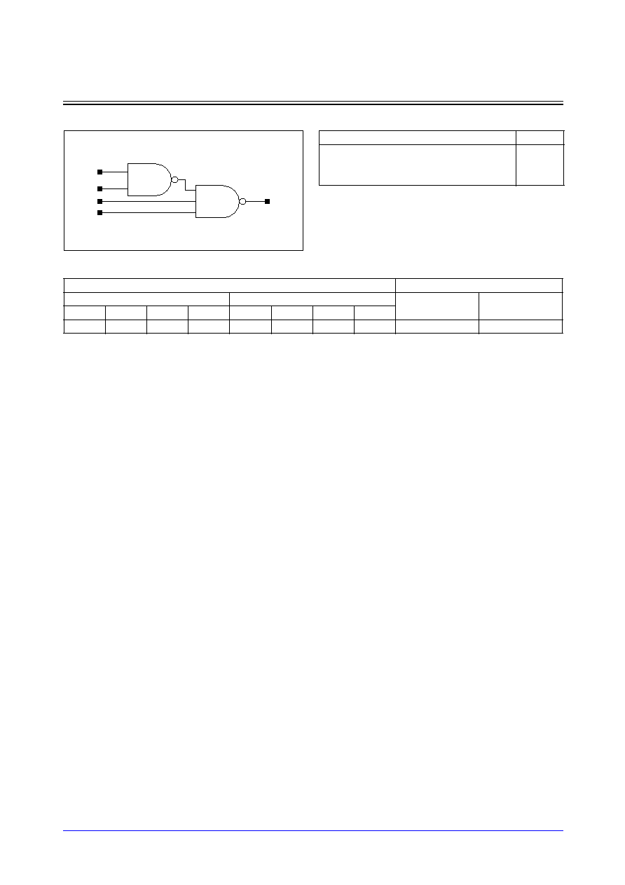
STDL131
3-188
Samsung ASIC
SCG15_LP/SCG15D2_LP
2-NAND into 3-NAND with 1X/2X Drive
Logic Symbol
Cell Data
Input Load (SL)
Gate Count
SCG15_LP
SCG15D2_LP
SCG15_LP
SCG15D2_LP
A
B
C
D
A
B
C
D
0.7
0.7
0.9
1.0
0.9
0.9
1.9
1.9
2.00
3.00
A
B
Y
C
D
Truth Table
A
B
C
D
Y
0
x
1
1
0
x
0
1
1
0
Other States
1
Samsung ASIC
3-189
STDL131
SCG15_LP/SCG15D2_LP
2-NAND into 3-NAND with 1X/2X Drive
Switching Characteristics
(Typical process, 25
∞
C, 1.8V, t
R
/t
F
= 0.19ns, SL: Standard Load)
SCG15_LP
SCG15D2_LP
Path
Parameter
Delay [ns]
SL = 2
Delay Equations [ns]
Group1*
Group2*
Group3*
A to Y
tR
0.146
0.077 + 0.035*SL
0.073 + 0.036*SL
0.069 + 0.036*SL
tF
0.154
0.080 + 0.037*SL
0.077 + 0.038*SL
0.074 + 0.038*SL
tPLH
0.193
0.157 + 0.018*SL
0.160 + 0.017*SL
0.161 + 0.017*SL
tPHL
0.203
0.163 + 0.020*SL
0.165 + 0.020*SL
0.166 + 0.020*SL
B to Y
tR
0.146
0.076 + 0.035*SL
0.074 + 0.035*SL
0.069 + 0.036*SL
tF
0.154
0.080 + 0.037*SL
0.078 + 0.038*SL
0.075 + 0.038*SL
tPLH
0.189
0.153 + 0.018*SL
0.156 + 0.017*SL
0.157 + 0.017*SL
tPHL
0.212
0.172 + 0.020*SL
0.174 + 0.020*SL
0.175 + 0.020*SL
C to Y
tR
0.163
0.097 + 0.033*SL
0.090 + 0.035*SL
0.079 + 0.036*SL
tF
0.159
0.087 + 0.036*SL
0.083 + 0.037*SL
0.077 + 0.038*SL
tPLH
0.135
0.100 + 0.017*SL
0.101 + 0.017*SL
0.101 + 0.017*SL
tPHL
0.121
0.079 + 0.021*SL
0.083 + 0.020*SL
0.084 + 0.020*SL
D to Y
tR
0.173
0.107 + 0.033*SL
0.100 + 0.035*SL
0.091 + 0.036*SL
tF
0.154
0.080 + 0.037*SL
0.078 + 0.037*SL
0.075 + 0.038*SL
tPLH
0.143
0.108 + 0.017*SL
0.109 + 0.017*SL
0.110 + 0.017*SL
tPHL
0.123
0.082 + 0.020*SL
0.084 + 0.020*SL
0.085 + 0.020*SL
*Group1 : SL < 4, *Group2 : 4 SL
<
<
=
= 8, *Group3 : 8 < SL
Path
Parameter
Delay [ns]
SL = 2
Delay Equations [ns]
Group1*
Group2*
Group3*
A to Y
tR
0.110
0.076 + 0.017*SL
0.074 + 0.017*SL
0.067 + 0.018*SL
tF
0.114
0.078 + 0.018*SL
0.077 + 0.018*SL
0.072 + 0.019*SL
tPLH
0.175
0.156 + 0.010*SL
0.160 + 0.009*SL
0.163 + 0.009*SL
tPHL
0.193
0.172 + 0.011*SL
0.175 + 0.010*SL
0.177 + 0.010*SL
B to Y
tR
0.109
0.076 + 0.017*SL
0.073 + 0.017*SL
0.067 + 0.018*SL
tF
0.114
0.079 + 0.018*SL
0.077 + 0.018*SL
0.072 + 0.019*SL
tPLH
0.172
0.153 + 0.010*SL
0.156 + 0.009*SL
0.159 + 0.009*SL
tPHL
0.203
0.181 + 0.011*SL
0.185 + 0.010*SL
0.187 + 0.010*SL
C to Y
tR
0.127
0.096 + 0.015*SL
0.091 + 0.017*SL
0.078 + 0.018*SL
tF
0.119
0.086 + 0.017*SL
0.080 + 0.018*SL
0.074 + 0.019*SL
tPLH
0.114
0.096 + 0.009*SL
0.098 + 0.009*SL
0.098 + 0.009*SL
tPHL
0.096
0.073 + 0.011*SL
0.079 + 0.010*SL
0.081 + 0.010*SL
D to Y
tR
0.137
0.106 + 0.016*SL
0.100 + 0.017*SL
0.089 + 0.018*SL
tF
0.112
0.077 + 0.018*SL
0.074 + 0.018*SL
0.071 + 0.019*SL
tPLH
0.123
0.105 + 0.009*SL
0.106 + 0.009*SL
0.108 + 0.009*SL
tPHL
0.098
0.076 + 0.011*SL
0.080 + 0.010*SL
0.083 + 0.010*SL
*Group1 : SL < 4, *Group2 : 4 SL
<
<
=
= 12, *Group3 : 12 < SL
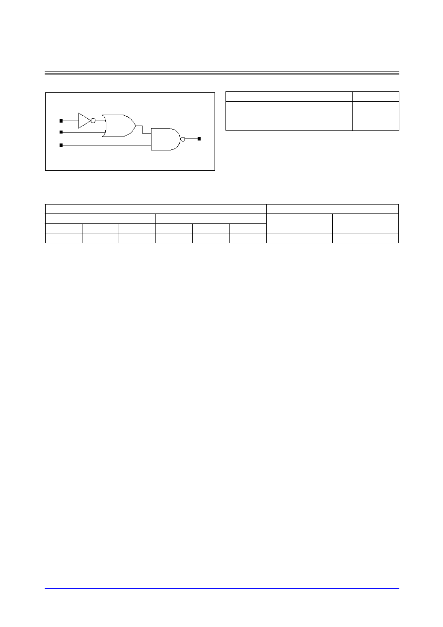
STDL131
3-190
Samsung ASIC
SCG16_LP/SCG16D2_LP
2-OR with one Inverted Input into 2-NAND with 1X/2X Drive
Logic Symbol
Cell Data
Input Load (SL)
Gate Count
SCG16_LP
SCG16D2_LP
SCG16_LP
SCG16D2_LP
A
B
C
A
B
C
0.7
1.1
1.1
1.0
2.1
2.1
2.00
3.00
A
B
Y
C
Truth Table
A
B
C
Y
0
x
1
0
x
1
1
0
Other States
1

Samsung ASIC
3-191
STDL131
SCG16_LP/SCG16D2_LP
2-OR with one Inverted Input into 2-NAND with 1X/2X Drive
Switching Characteristics
(Typical process, 25
∞
C, 1.8V, t
R
/t
F
= 0.19ns, SL: Standard Load)
SCG16_LP
SCG16D2_LP
Path
Parameter
Delay [ns]
SL = 2
Delay Equations [ns]
Group1*
Group2*
Group3*
A to Y
tR
0.227
0.118 + 0.054*SL
0.118 + 0.054*SL
0.118 + 0.054*SL
tF
0.140
0.077 + 0.032*SL
0.075 + 0.032*SL
0.071 + 0.033*SL
tPLH
0.188
0.134 + 0.027*SL
0.135 + 0.027*SL
0.137 + 0.026*SL
tPHL
0.208
0.172 + 0.018*SL
0.175 + 0.017*SL
0.176 + 0.017*SL
B to Y
tR
0.231
0.125 + 0.053*SL
0.121 + 0.054*SL
0.118 + 0.054*SL
tF
0.169
0.111 + 0.029*SL
0.104 + 0.031*SL
0.097 + 0.032*SL
tPLH
0.179
0.126 + 0.027*SL
0.126 + 0.027*SL
0.127 + 0.026*SL
tPHL
0.136
0.101 + 0.018*SL
0.102 + 0.017*SL
0.104 + 0.017*SL
C to Y
tR
0.141
0.094 + 0.024*SL
0.088 + 0.025*SL
0.080 + 0.026*SL
tF
0.162
0.101 + 0.031*SL
0.098 + 0.031*SL
0.093 + 0.032*SL
tPLH
0.122
0.096 + 0.013*SL
0.098 + 0.013*SL
0.098 + 0.013*SL
tPHL
0.142
0.106 + 0.018*SL
0.108 + 0.017*SL
0.110 + 0.017*SL
*Group1 : SL < 4, *Group2 : 4 SL
<
<
=
= 8, *Group3 : 8 < SL
Path
Parameter
Delay [ns]
SL = 2
Delay Equations [ns]
Group1*
Group2*
Group3*
A to Y
tR
0.166
0.113 + 0.027*SL
0.111 + 0.027*SL
0.111 + 0.027*SL
tF
0.108
0.077 + 0.016*SL
0.076 + 0.016*SL
0.072 + 0.016*SL
tPLH
0.165
0.137 + 0.014*SL
0.138 + 0.013*SL
0.140 + 0.013*SL
tPHL
0.200
0.181 + 0.010*SL
0.184 + 0.009*SL
0.187 + 0.009*SL
B to Y
tR
0.172
0.121 + 0.026*SL
0.117 + 0.027*SL
0.112 + 0.027*SL
tF
0.136
0.107 + 0.015*SL
0.105 + 0.015*SL
0.096 + 0.016*SL
tPLH
0.150
0.124 + 0.013*SL
0.124 + 0.013*SL
0.125 + 0.013*SL
tPHL
0.116
0.098 + 0.009*SL
0.100 + 0.009*SL
0.102 + 0.009*SL
C to Y
tR
0.116
0.095 + 0.011*SL
0.089 + 0.012*SL
0.079 + 0.013*SL
tF
0.128
0.097 + 0.015*SL
0.096 + 0.016*SL
0.091 + 0.016*SL
tPLH
0.107
0.093 + 0.007*SL
0.096 + 0.006*SL
0.096 + 0.006*SL
tPHL
0.121
0.103 + 0.009*SL
0.105 + 0.009*SL
0.107 + 0.009*SL
*Group1 : SL < 4, *Group2 : 4 SL
<
<
=
= 12, *Group3 : 12 < SL

STDL131
3-192
Samsung ASIC
SCG17_LP/SCG17D2_LP
2-AND into 2-NOR into 2-NAND with 1X/2X Drive
Logic Symbol
Cell Data
Input Load (SL)
Gate Count
SCG17_LP
SCG17D2_LP
SCG17_LP
SCG17D2_LP
A
B
C
D
A
B
C
D
0.7
0.7
0.7
1.0
1.1
1.0
1.0
2.3
2.00
2.67
A
B
C
D
Y
Truth Table
A
B
C
D
Y
0
x
0
1
0
x
0
0
1
0
Other States
1
Samsung ASIC
3-193
STDL131
SCG17_LP/SCG17D2_LP
2-AND into 2-NOR into 2-NAND with 1X/2X Drive
Switching Characteristics
(Typical process, 25
∞
C, 1.8V, t
R
/t
F
= 0.19ns, SL: Standard Load)
SCG17_LP
SCG17D2_LP
Path
Parameter
Delay [ns]
SL = 2
Delay Equations [ns]
Group1*
Group2*
Group3*
A to Y
tR
0.131
0.063 + 0.034*SL
0.056 + 0.036*SL
0.052 + 0.036*SL
tF
0.121
0.069 + 0.026*SL
0.072 + 0.025*SL
0.069 + 0.026*SL
tPLH
0.189
0.152 + 0.018*SL
0.157 + 0.017*SL
0.159 + 0.017*SL
tPHL
0.230
0.194 + 0.018*SL
0.205 + 0.016*SL
0.214 + 0.014*SL
B to Y
tR
0.131
0.063 + 0.034*SL
0.057 + 0.035*SL
0.053 + 0.036*SL
tF
0.124
0.073 + 0.026*SL
0.073 + 0.025*SL
0.071 + 0.026*SL
tPLH
0.186
0.149 + 0.018*SL
0.154 + 0.017*SL
0.155 + 0.017*SL
tPHL
0.248
0.211 + 0.019*SL
0.223 + 0.016*SL
0.232 + 0.014*SL
C to Y
tR
0.130
0.061 + 0.035*SL
0.058 + 0.035*SL
0.052 + 0.036*SL
tF
0.124
0.071 + 0.026*SL
0.075 + 0.025*SL
0.071 + 0.026*SL
tPLH
0.222
0.186 + 0.018*SL
0.189 + 0.017*SL
0.191 + 0.017*SL
tPHL
0.285
0.248 + 0.019*SL
0.260 + 0.016*SL
0.269 + 0.014*SL
D to Y
tR
0.149
0.085 + 0.032*SL
0.076 + 0.034*SL
0.064 + 0.036*SL
tF
0.108
0.059 + 0.025*SL
0.054 + 0.026*SL
0.051 + 0.026*SL
tPLH
0.126
0.091 + 0.017*SL
0.093 + 0.017*SL
0.093 + 0.017*SL
tPHL
0.087
0.054 + 0.017*SL
0.062 + 0.014*SL
0.065 + 0.014*SL
*Group1 : SL < 4, *Group2 : 4 SL
<
<
=
= 8, *Group3 : 8 < SL
Path
Parameter
Delay [ns]
SL = 2
Delay Equations [ns]
Group1*
Group2*
Group3*
A to Y
tR
0.096
0.070 + 0.013*SL
0.072 + 0.012*SL
0.065 + 0.013*SL
tF
0.105
0.078 + 0.013*SL
0.079 + 0.013*SL
0.079 + 0.013*SL
tPLH
0.199
0.182 + 0.009*SL
0.188 + 0.007*SL
0.196 + 0.006*SL
tPHL
0.235
0.214 + 0.010*SL
0.221 + 0.009*SL
0.234 + 0.007*SL
B to Y
tR
0.096
0.071 + 0.012*SL
0.072 + 0.012*SL
0.065 + 0.013*SL
tF
0.108
0.080 + 0.014*SL
0.083 + 0.013*SL
0.083 + 0.013*SL
tPLH
0.196
0.178 + 0.009*SL
0.185 + 0.007*SL
0.193 + 0.006*SL
tPHL
0.249
0.228 + 0.011*SL
0.236 + 0.009*SL
0.249 + 0.007*SL
C to Y
tR
0.095
0.072 + 0.012*SL
0.070 + 0.012*SL
0.062 + 0.013*SL
tF
0.108
0.080 + 0.014*SL
0.083 + 0.013*SL
0.083 + 0.013*SL
tPLH
0.238
0.221 + 0.008*SL
0.227 + 0.007*SL
0.234 + 0.006*SL
tPHL
0.286
0.265 + 0.011*SL
0.273 + 0.009*SL
0.286 + 0.007*SL
D to Y
tR
0.105
0.084 + 0.010*SL
0.079 + 0.012*SL
0.066 + 0.013*SL
tF
0.089
0.063 + 0.013*SL
0.063 + 0.013*SL
0.057 + 0.013*SL
tPLH
0.095
0.079 + 0.008*SL
0.085 + 0.006*SL
0.086 + 0.006*SL
tPHL
0.075
0.057 + 0.009*SL
0.063 + 0.008*SL
0.069 + 0.007*SL
*Group1 : SL < 4, *Group2 : 4 SL
<
<
=
= 12, *Group3 : 12 < SL
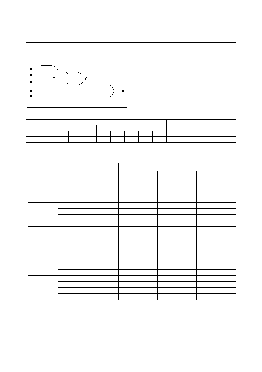
STDL131
3-194
Samsung ASIC
SCG18_LP/SCG18D2_LP
2-AND into 2-NOR into 3-NAND with 1X/2X Drive
Logic Symbol
Cell Data
Switching Characteristics
(Typical process, 25
∞
C, 1.8V, t
R
/t
F
= 0.19ns, SL: Standard Load)
SCG18_LP
Input Load (SL)
Gate Count
SCG18_LP
SCG18D2_LP
SCG18_LP
SCG18D2_LP
A
B
C
D
E
A
B
C
D
E
0.8
0.8
0.8
1.0
1.0
1.0
1.0
1.0
1.9
1.9
2.33
3.33
A
B
C
D
E
Y
Path
Parameter
Delay [ns]
SL = 2
Delay Equations [ns]
Group1*
Group2*
Group3*
A to Y
tR
0.158
0.090 + 0.034*SL
0.085 + 0.035*SL
0.079 + 0.036*SL
tF
0.168
0.096 + 0.036*SL
0.095 + 0.036*SL
0.092 + 0.037*SL
tPLH
0.234
0.196 + 0.019*SL
0.201 + 0.017*SL
0.204 + 0.017*SL
tPHL
0.247
0.203 + 0.022*SL
0.210 + 0.020*SL
0.215 + 0.019*SL
B to Y
tR
0.157
0.089 + 0.034*SL
0.084 + 0.035*SL
0.079 + 0.036*SL
tF
0.169
0.098 + 0.036*SL
0.096 + 0.036*SL
0.093 + 0.037*SL
tPLH
0.230
0.193 + 0.019*SL
0.198 + 0.017*SL
0.201 + 0.017*SL
tPHL
0.257
0.213 + 0.022*SL
0.221 + 0.020*SL
0.226 + 0.019*SL
C to Y
tR
0.151
0.083 + 0.034*SL
0.076 + 0.036*SL
0.073 + 0.036*SL
tF
0.170
0.098 + 0.036*SL
0.098 + 0.036*SL
0.093 + 0.036*SL
tPLH
0.247
0.211 + 0.018*SL
0.214 + 0.017*SL
0.215 + 0.017*SL
tPHL
0.294
0.251 + 0.022*SL
0.258 + 0.020*SL
0.263 + 0.019*SL
D to Y
tR
0.165
0.099 + 0.033*SL
0.093 + 0.035*SL
0.081 + 0.036*SL
tF
0.160
0.089 + 0.035*SL
0.085 + 0.036*SL
0.080 + 0.037*SL
tPLH
0.136
0.101 + 0.017*SL
0.102 + 0.017*SL
0.102 + 0.017*SL
tPHL
0.121
0.081 + 0.020*SL
0.084 + 0.019*SL
0.086 + 0.019*SL
E to Y
tR
0.176
0.110 + 0.033*SL
0.102 + 0.035*SL
0.093 + 0.036*SL
tF
0.155
0.083 + 0.036*SL
0.081 + 0.037*SL
0.078 + 0.037*SL
tPLH
0.144
0.109 + 0.017*SL
0.110 + 0.017*SL
0.111 + 0.017*SL
tPHL
0.121
0.081 + 0.020*SL
0.084 + 0.019*SL
0.085 + 0.019*SL
*Group1 : SL < 4, *Group2 : 4 SL
<
<
=
= 8, *Group3 : 8 < SL
Truth Table
A
B
C
D
E
Y
0
x
0
1
1
0
x
0
0
1
1
0
Other States
1
Samsung ASIC
3-195
STDL131
SCG18_LP/SCG18D2_LP
2-AND into 2-NOR into 3-NAND with 1X/2X Drive
Switching Characteristics
(Typical process, 25
∞
C, 1.8V, t
R
/t
F
= 0.19ns, SL: Standard Load)
SCG18D2_LP
Path
Parameter
Delay [ns]
SL = 2
Delay Equations [ns]
Group1*
Group2*
Group3*
A to Y
tR
0.119
0.086 + 0.016*SL
0.083 + 0.017*SL
0.076 + 0.018*SL
tF
0.129
0.093 + 0.018*SL
0.094 + 0.018*SL
0.091 + 0.018*SL
tPLH
0.220
0.199 + 0.011*SL
0.205 + 0.009*SL
0.210 + 0.009*SL
tPHL
0.236
0.211 + 0.012*SL
0.218 + 0.011*SL
0.228 + 0.010*SL
B to Y
tR
0.120
0.087 + 0.016*SL
0.084 + 0.017*SL
0.076 + 0.018*SL
tF
0.130
0.093 + 0.018*SL
0.095 + 0.018*SL
0.092 + 0.018*SL
tPLH
0.216
0.195 + 0.011*SL
0.201 + 0.009*SL
0.207 + 0.009*SL
tPHL
0.247
0.222 + 0.012*SL
0.229 + 0.011*SL
0.239 + 0.010*SL
C to Y
tR
0.113
0.080 + 0.016*SL
0.077 + 0.017*SL
0.069 + 0.018*SL
tF
0.130
0.092 + 0.019*SL
0.095 + 0.018*SL
0.092 + 0.018*SL
tPLH
0.238
0.218 + 0.010*SL
0.222 + 0.009*SL
0.225 + 0.009*SL
tPHL
0.283
0.258 + 0.012*SL
0.265 + 0.011*SL
0.275 + 0.010*SL
D to Y
tR
0.127
0.096 + 0.015*SL
0.090 + 0.017*SL
0.078 + 0.018*SL
tF
0.118
0.085 + 0.017*SL
0.080 + 0.018*SL
0.075 + 0.018*SL
tPLH
0.113
0.095 + 0.009*SL
0.097 + 0.009*SL
0.098 + 0.009*SL
tPHL
0.095
0.072 + 0.011*SL
0.078 + 0.010*SL
0.081 + 0.010*SL
E to Y
tR
0.136
0.105 + 0.016*SL
0.100 + 0.017*SL
0.089 + 0.018*SL
tF
0.111
0.074 + 0.018*SL
0.074 + 0.018*SL
0.072 + 0.019*SL
tPLH
0.122
0.104 + 0.009*SL
0.105 + 0.009*SL
0.106 + 0.009*SL
tPHL
0.096
0.074 + 0.011*SL
0.078 + 0.010*SL
0.081 + 0.010*SL
*Group1 : SL < 4, *Group2 : 4 SL
<
<
=
= 12, *Group3 : 12 < SL
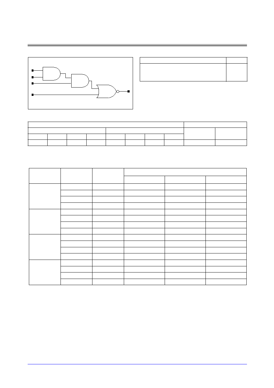
STDL131
3-196
Samsung ASIC
SCG19_LP/SCG19D2_LP
2-AND into 2-AND into 2-NOR with 1X/2X Drive
Logic Symbol
Cell Data
Switching Characteristics
(Typical process, 25
∞
C, 1.8V, t
R
/t
F
= 0.19ns, SL: Standard Load)
SCG19_LP
Input Load (SL)
Gate Count
SCG19_LP
SCG19D2_LP
SCG19_LP
SCG19D2_LP
A
B
C
D
A
B
C
D
0.6
0.6
1.1
1.1
0.6
0.6
2.2
2.3
2.67
3.67
A
B
C
D
Y
Path
Parameter
Delay [ns]
SL = 2
Delay Equations [ns]
Group1*
Group2*
Group3*
A to Y
tR
0.220
0.111 + 0.054*SL
0.110 + 0.055*SL
0.111 + 0.054*SL
tF
0.110
0.060 + 0.025*SL
0.055 + 0.026*SL
0.054 + 0.026*SL
tPLH
0.294
0.240 + 0.027*SL
0.242 + 0.027*SL
0.243 + 0.026*SL
tPHL
0.225
0.195 + 0.015*SL
0.198 + 0.014*SL
0.200 + 0.014*SL
B to Y
tR
0.220
0.111 + 0.054*SL
0.110 + 0.055*SL
0.111 + 0.054*SL
tF
0.110
0.060 + 0.025*SL
0.055 + 0.026*SL
0.054 + 0.026*SL
tPLH
0.310
0.256 + 0.027*SL
0.258 + 0.027*SL
0.260 + 0.026*SL
tPHL
0.223
0.194 + 0.015*SL
0.197 + 0.014*SL
0.198 + 0.014*SL
C to Y
tR
0.248
0.144 + 0.052*SL
0.136 + 0.054*SL
0.128 + 0.055*SL
tF
0.117
0.069 + 0.024*SL
0.064 + 0.025*SL
0.059 + 0.026*SL
tPLH
0.167
0.113 + 0.027*SL
0.114 + 0.027*SL
0.115 + 0.027*SL
tPHL
0.097
0.066 + 0.016*SL
0.072 + 0.014*SL
0.073 + 0.014*SL
D to Y
tR
0.242
0.135 + 0.054*SL
0.131 + 0.055*SL
0.130 + 0.055*SL
tF
0.119
0.090 + 0.015*SL
0.086 + 0.016*SL
0.079 + 0.016*SL
tPLH
0.204
0.150 + 0.027*SL
0.151 + 0.027*SL
0.152 + 0.027*SL
tPHL
0.107
0.085 + 0.011*SL
0.089 + 0.010*SL
0.090 + 0.010*SL
*Group1 : SL < 4, *Group2 : 4 SL
<
<
=
= 8, *Group3 : 8 < SL
Truth Table
A
B
C
D
Y
1
1
1
x
0
x
x
x
1
0
Other States
1

Samsung ASIC
3-197
STDL131
SCG19_LP/SCG19D2_LP
2-AND into 2-AND into 2-NOR with 1X/2X Drive
Switching Characteristics
(Typical process, 25
∞
C, 1.8V, t
R
/t
F
= 0.19ns, SL: Standard Load)
SCG19D2_LP
Path
Parameter
Delay [ns]
SL = 2
Delay Equations [ns]
Group1*
Group2*
Group3*
A to Y
tR
0.162
0.109 + 0.027*SL
0.108 + 0.027*SL
0.107 + 0.027*SL
tF
0.088
0.063 + 0.012*SL
0.061 + 0.013*SL
0.058 + 0.013*SL
tPLH
0.292
0.264 + 0.014*SL
0.266 + 0.013*SL
0.268 + 0.013*SL
tPHL
0.241
0.225 + 0.008*SL
0.228 + 0.007*SL
0.232 + 0.007*SL
B to Y
tR
0.162
0.110 + 0.026*SL
0.107 + 0.027*SL
0.106 + 0.027*SL
tF
0.088
0.064 + 0.012*SL
0.061 + 0.013*SL
0.057 + 0.013*SL
tPLH
0.306
0.278 + 0.014*SL
0.280 + 0.013*SL
0.282 + 0.013*SL
tPHL
0.238
0.222 + 0.008*SL
0.225 + 0.007*SL
0.229 + 0.007*SL
C to Y
tR
0.192
0.141 + 0.025*SL
0.137 + 0.026*SL
0.126 + 0.027*SL
tF
0.092
0.067 + 0.013*SL
0.067 + 0.013*SL
0.061 + 0.013*SL
tPLH
0.138
0.112 + 0.013*SL
0.112 + 0.013*SL
0.113 + 0.013*SL
tPHL
0.081
0.064 + 0.009*SL
0.069 + 0.007*SL
0.074 + 0.007*SL
D to Y
tR
0.184
0.132 + 0.026*SL
0.129 + 0.027*SL
0.125 + 0.027*SL
tF
0.095
0.079 + 0.008*SL
0.082 + 0.007*SL
0.074 + 0.008*SL
tPLH
0.172
0.145 + 0.013*SL
0.146 + 0.013*SL
0.147 + 0.013*SL
tPHL
0.093
0.081 + 0.006*SL
0.085 + 0.005*SL
0.087 + 0.005*SL
*Group1 : SL < 4, *Group2 : 4 SL
<
<
=
= 12, *Group3 : 12 < SL
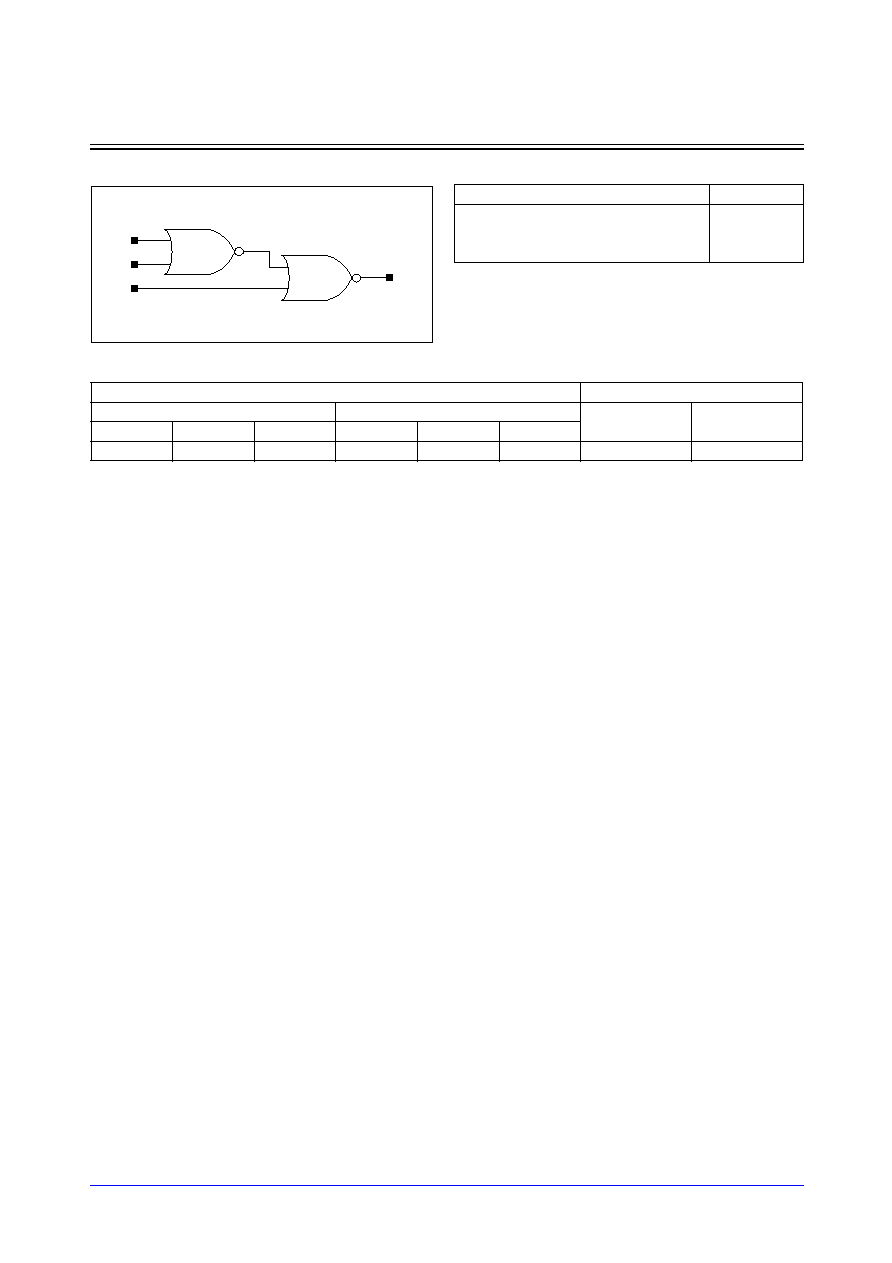
STDL131
3-198
Samsung ASIC
SCG20_LP/SCG20D2_LP
2-NOR into 2-NOR with 1X/2X Drive
Logic Symbol
Cell Data
Input Load (SL)
Gate Count
SCG20_LP
SCG20D2_LP
SCG20_LP
SCG20D2_LP
A
B
C
A
B
C
0.8
0.8
1.1
1.1
1.1
2.3
1.67
2.33
Y
C
A
B
Truth Table
A
B
C
Y
1
x
0
1
x
1
0
1
Other States
0

Samsung ASIC
3-199
STDL131
SCG20_LP/SCG20D2_LP
2-NOR into 2-NOR with 1X/2X Drive
Switching Characteristics
(Typical process, 25
∞
C, 1.8V, t
R
/t
F
= 0.19ns, SL: Standard Load)
SCG20_LP
SCG20D2_LP
Path
Parameter
Delay [ns]
SL = 2
Delay Equations [ns]
Group1*
Group2*
Group3*
A to Y
tR
0.193
0.087 + 0.053*SL
0.084 + 0.054*SL
0.083 + 0.054*SL
tF
0.088
0.056 + 0.016*SL
0.056 + 0.016*SL
0.059 + 0.015*SL
tPLH
0.183
0.130 + 0.027*SL
0.131 + 0.026*SL
0.132 + 0.026*SL
tPHL
0.208
0.182 + 0.013*SL
0.192 + 0.011*SL
0.201 + 0.009*SL
B to Y
tR
0.193
0.086 + 0.053*SL
0.084 + 0.054*SL
0.084 + 0.054*SL
tF
0.087
0.053 + 0.017*SL
0.060 + 0.015*SL
0.058 + 0.015*SL
tPLH
0.197
0.143 + 0.027*SL
0.144 + 0.026*SL
0.146 + 0.026*SL
tPHL
0.227
0.201 + 0.013*SL
0.211 + 0.011*SL
0.220 + 0.009*SL
C to Y
tR
0.197
0.093 + 0.052*SL
0.088 + 0.053*SL
0.084 + 0.054*SL
tF
0.097
0.069 + 0.014*SL
0.069 + 0.014*SL
0.059 + 0.015*SL
tPLH
0.163
0.110 + 0.026*SL
0.111 + 0.026*SL
0.111 + 0.026*SL
tPHL
0.085
0.062 + 0.012*SL
0.072 + 0.009*SL
0.074 + 0.009*SL
*Group1 : SL < 4, *Group2 : 4 SL
<
<
=
= 8, *Group3 : 8 < SL
Path
Parameter
Delay [ns]
SL = 2
Delay Equations [ns]
Group1*
Group2*
Group3*
A to Y
tR
0.130
0.079 + 0.026*SL
0.074 + 0.027*SL
0.073 + 0.027*SL
tF
0.075
0.056 + 0.009*SL
0.062 + 0.008*SL
0.065 + 0.008*SL
tPLH
0.157
0.130 + 0.014*SL
0.131 + 0.013*SL
0.132 + 0.013*SL
tPHL
0.212
0.195 + 0.009*SL
0.205 + 0.006*SL
0.219 + 0.005*SL
B to Y
tR
0.131
0.078 + 0.026*SL
0.076 + 0.027*SL
0.073 + 0.027*SL
tF
0.076
0.058 + 0.009*SL
0.062 + 0.008*SL
0.065 + 0.008*SL
tPLH
0.169
0.142 + 0.014*SL
0.143 + 0.013*SL
0.145 + 0.013*SL
tPHL
0.232
0.215 + 0.009*SL
0.224 + 0.006*SL
0.238 + 0.005*SL
C to Y
tR
0.136
0.084 + 0.026*SL
0.081 + 0.026*SL
0.075 + 0.027*SL
tF
0.080
0.066 + 0.007*SL
0.066 + 0.007*SL
0.061 + 0.007*SL
tPLH
0.131
0.103 + 0.014*SL
0.105 + 0.013*SL
0.106 + 0.013*SL
tPHL
0.069
0.055 + 0.007*SL
0.063 + 0.005*SL
0.071 + 0.004*SL
*Group1 : SL < 4, *Group2 : 4 SL
<
<
=
= 12, *Group3 : 12 < SL

STDL131
3-200
Samsung ASIC
SCG21_LP/SCG21D2_LP
2-NOR into 3-NOR with 1X/2X Drive
Logic Symbol
Cell Data
Input Load (SL)
Gate Count
SCG21_LP
SCG21D2_LP
SCG21_LP
SCG21D2_LP
A
B
C
D
A
B
C
D
0.8
0.8
1.0
1.1
1.1
1.1
2.0
2.0
2.00
3.00
Y
C
A
B
D
Truth Table
A
B
C
D
Y
1
x
0
0
1
x
1
0
0
1
Other States
0

Samsung ASIC
3-201
STDL131
SCG21_LP/SCG21D2_LP
2-NOR into 3-NOR with 1X/2X Drive
Switching Characteristics
(Typical process, 25
∞
C, 1.8V, t
R
/t
F
= 0.19ns, SL: Standard Load)
SCG21_LP
SCG21D2_LP
Path
Parameter
Delay [ns]
SL = 2
Delay Equations [ns]
Group1*
Group2*
Group3*
A to Y
tR
0.304
0.141 + 0.082*SL
0.142 + 0.081*SL
0.147 + 0.081*SL
tF
0.118
0.067 + 0.026*SL
0.069 + 0.025*SL
0.063 + 0.026*SL
tPLH
0.221
0.140 + 0.040*SL
0.142 + 0.040*SL
0.144 + 0.040*SL
tPHL
0.237
0.200 + 0.018*SL
0.210 + 0.016*SL
0.217 + 0.015*SL
B to Y
tR
0.305
0.141 + 0.082*SL
0.143 + 0.081*SL
0.147 + 0.081*SL
tF
0.119
0.068 + 0.025*SL
0.067 + 0.026*SL
0.064 + 0.026*SL
tPLH
0.235
0.154 + 0.040*SL
0.156 + 0.040*SL
0.158 + 0.040*SL
tPHL
0.256
0.219 + 0.018*SL
0.229 + 0.016*SL
0.237 + 0.015*SL
C to Y
tR
0.313
0.154 + 0.079*SL
0.150 + 0.080*SL
0.148 + 0.081*SL
tF
0.129
0.082 + 0.023*SL
0.075 + 0.025*SL
0.066 + 0.026*SL
tPLH
0.223
0.144 + 0.040*SL
0.144 + 0.040*SL
0.145 + 0.040*SL
tPHL
0.121
0.090 + 0.016*SL
0.093 + 0.015*SL
0.094 + 0.015*SL
D to Y
tR
0.311
0.152 + 0.080*SL
0.149 + 0.080*SL
0.148 + 0.081*SL
tF
0.147
0.098 + 0.025*SL
0.094 + 0.025*SL
0.087 + 0.026*SL
tPLH
0.245
0.165 + 0.040*SL
0.166 + 0.040*SL
0.167 + 0.040*SL
tPHL
0.129
0.097 + 0.016*SL
0.099 + 0.016*SL
0.103 + 0.015*SL
*Group1 : SL < 4, *Group2 : 4 SL
<
<
=
= 8, *Group3 : 8 < SL
Path
Parameter
Delay [ns]
SL = 2
Delay Equations [ns]
Group1*
Group2*
Group3*
A to Y
tR
0.203
0.122 + 0.041*SL
0.121 + 0.041*SL
0.125 + 0.040*SL
tF
0.092
0.065 + 0.013*SL
0.068 + 0.013*SL
0.065 + 0.013*SL
tPLH
0.169
0.129 + 0.020*SL
0.129 + 0.020*SL
0.132 + 0.020*SL
tPHL
0.229
0.206 + 0.011*SL
0.216 + 0.009*SL
0.230 + 0.008*SL
B to Y
tR
0.203
0.122 + 0.041*SL
0.121 + 0.041*SL
0.126 + 0.040*SL
tF
0.092
0.065 + 0.014*SL
0.068 + 0.013*SL
0.066 + 0.013*SL
tPLH
0.182
0.141 + 0.020*SL
0.142 + 0.020*SL
0.144 + 0.020*SL
tPHL
0.247
0.224 + 0.011*SL
0.234 + 0.009*SL
0.248 + 0.008*SL
C to Y
tR
0.215
0.138 + 0.039*SL
0.132 + 0.040*SL
0.128 + 0.040*SL
tF
0.099
0.075 + 0.012*SL
0.074 + 0.012*SL
0.063 + 0.013*SL
tPLH
0.174
0.134 + 0.020*SL
0.135 + 0.020*SL
0.136 + 0.020*SL
tPHL
0.100
0.082 + 0.009*SL
0.087 + 0.008*SL
0.090 + 0.007*SL
D to Y
tR
0.212
0.133 + 0.039*SL
0.131 + 0.040*SL
0.128 + 0.040*SL
tF
0.117
0.093 + 0.012*SL
0.091 + 0.012*SL
0.084 + 0.013*SL
tPLH
0.197
0.156 + 0.020*SL
0.157 + 0.020*SL
0.158 + 0.020*SL
tPHL
0.108
0.091 + 0.009*SL
0.094 + 0.008*SL
0.098 + 0.008*SL
*Group1 : SL < 4, *Group2 : 4 SL
<
<
=
= 12, *Group3 : 12 < SL

STDL131
3-202
Samsung ASIC
SCG22_LP/SCG22D2_LP
2-NAND into 2-OR into 2-NAND with 1X/2X Drive
Logic Symbol
Cell Data
Input Load (SL)
Gate Count
SCG22_LP
SCG22D2_LP
SCG22_LP
SCG22D2_LP
A
B
C
D
A
B
C
D
0.6
0.7
1.1
1.1
1.1
1.1
2.2
2.2
2.33
3.33
A
B
C
D
Y
Truth Table
A
B
C
D
Y
1
1
0
x
1
x
x
x
0
1
Other States
0

Samsung ASIC
3-203
STDL131
SCG22_LP/SCG22D2_LP
2-NAND into 2-OR into 2-NAND with 1X/2X Drive
Switching Characteristics
(Typical process, 25
∞
C, 1.8V, t
R
/t
F
= 0.19ns, SL: Standard Load)
SCG22_LP
SCG22D2_LP
Path
Parameter
Delay [ns]
SL = 2
Delay Equations [ns]
Group1*
Group2*
Group3*
A to Y
tR
0.237
0.131 + 0.053*SL
0.127 + 0.054*SL
0.125 + 0.054*SL
tF
0.143
0.081 + 0.031*SL
0.078 + 0.032*SL
0.075 + 0.032*SL
tPLH
0.231
0.177 + 0.027*SL
0.179 + 0.027*SL
0.180 + 0.026*SL
tPHL
0.220
0.184 + 0.018*SL
0.187 + 0.017*SL
0.189 + 0.017*SL
B to Y
tR
0.237
0.131 + 0.053*SL
0.128 + 0.054*SL
0.125 + 0.054*SL
tF
0.143
0.081 + 0.031*SL
0.080 + 0.031*SL
0.075 + 0.032*SL
tPLH
0.229
0.175 + 0.027*SL
0.177 + 0.027*SL
0.178 + 0.026*SL
tPHL
0.231
0.195 + 0.018*SL
0.198 + 0.017*SL
0.200 + 0.017*SL
C to Y
tR
0.238
0.132 + 0.053*SL
0.128 + 0.054*SL
0.124 + 0.054*SL
tF
0.170
0.112 + 0.029*SL
0.106 + 0.030*SL
0.099 + 0.031*SL
tPLH
0.183
0.129 + 0.027*SL
0.130 + 0.027*SL
0.131 + 0.026*SL
tPHL
0.135
0.100 + 0.017*SL
0.102 + 0.017*SL
0.104 + 0.017*SL
D to Y
tR
0.144
0.097 + 0.023*SL
0.090 + 0.025*SL
0.083 + 0.026*SL
tF
0.162
0.102 + 0.030*SL
0.099 + 0.031*SL
0.094 + 0.031*SL
tPLH
0.124
0.098 + 0.013*SL
0.099 + 0.013*SL
0.100 + 0.013*SL
tPHL
0.141
0.106 + 0.018*SL
0.108 + 0.017*SL
0.110 + 0.017*SL
*Group1 : SL < 4, *Group2 : 4 SL
<
<
=
= 8, *Group3 : 8 < SL
Path
Parameter
Delay [ns]
SL = 2
Delay Equations [ns]
Group1*
Group2*
Group3*
A to Y
tR
0.173
0.122 + 0.025*SL
0.118 + 0.027*SL
0.114 + 0.027*SL
tF
0.105
0.075 + 0.015*SL
0.073 + 0.016*SL
0.068 + 0.016*SL
tPLH
0.203
0.175 + 0.014*SL
0.177 + 0.013*SL
0.179 + 0.013*SL
tPHL
0.190
0.171 + 0.010*SL
0.174 + 0.009*SL
0.177 + 0.009*SL
B to Y
tR
0.173
0.122 + 0.026*SL
0.118 + 0.027*SL
0.114 + 0.027*SL
tF
0.105
0.074 + 0.016*SL
0.074 + 0.016*SL
0.070 + 0.016*SL
tPLH
0.199
0.171 + 0.014*SL
0.173 + 0.013*SL
0.175 + 0.013*SL
tPHL
0.198
0.179 + 0.010*SL
0.182 + 0.009*SL
0.185 + 0.009*SL
C to Y
tR
0.173
0.121 + 0.026*SL
0.119 + 0.026*SL
0.113 + 0.027*SL
tF
0.135
0.107 + 0.014*SL
0.104 + 0.015*SL
0.094 + 0.016*SL
tPLH
0.150
0.123 + 0.014*SL
0.125 + 0.013*SL
0.126 + 0.013*SL
tPHL
0.114
0.096 + 0.009*SL
0.098 + 0.009*SL
0.100 + 0.008*SL
D to Y
tR
0.115
0.094 + 0.011*SL
0.088 + 0.012*SL
0.078 + 0.013*SL
tF
0.127
0.097 + 0.015*SL
0.096 + 0.015*SL
0.090 + 0.016*SL
tPLH
0.106
0.092 + 0.007*SL
0.095 + 0.006*SL
0.096 + 0.006*SL
tPHL
0.117
0.099 + 0.009*SL
0.101 + 0.009*SL
0.104 + 0.008*SL
*Group1 : SL < 4, *Group2 : 4 SL
<
<
=
= 12, *Group3 : 12 < SL

STDL131
3-204
Samsung ASIC
DL1D2_LP
1ns Delay Cell with 2X Drive
Logic Symbol
Switching Characteristics
(Typical process, 25
∞
C, 1.8V, t
R
/t
F
= 0.19ns, SL: Standard Load)
DL1D2_LP
A
Y
Path
Parameter
Delay [ns]
SL = 2
Delay Equations [ns]
Group1*
Group2*
Group3*
A to Y
tR
0.066
0.043 + 0.012*SL
0.040 + 0.012*SL
0.033 + 0.013*SL
tF
0.059
0.038 + 0.011*SL
0.041 + 0.010*SL
0.034 + 0.011*SL
tPLH
0.930
0.915 + 0.007*SL
0.920 + 0.006*SL
0.922 + 0.006*SL
tPHL
0.894
0.879 + 0.008*SL
0.885 + 0.006*SL
0.890 + 0.006*SL
*Group1 : SL < 4, *Group2 : 4 SL
<
<
=
= 12, *Group3 : 12 < SL
Truth Table
Cell Data
A
Y
0
0
1
1
Input Load (SL)
Gate Count
DL1D2_LP
DL1D2_LP
A
4.00
0.5
Samsung ASIC
3-205
STDL131
DL2D2_LP
2ns Delay Cell with 2X Drive
Logic Symbol
Switching Characteristics
(Typical process, 25
∞
C, 1.8V, t
R
/t
F
= 0.19ns, SL: Standard Load)
DL2D2_LP
A
Y
Path
Parameter
Delay [ns]
SL = 2
Delay Equations [ns]
Group1*
Group2*
Group3*
A to Y
tR
0.069
0.046 + 0.011*SL
0.042 + 0.012*SL
0.034 + 0.013*SL
tF
0.065
0.044 + 0.010*SL
0.045 + 0.010*SL
0.039 + 0.010*SL
tPLH
1.961
1.945 + 0.008*SL
1.950 + 0.006*SL
1.953 + 0.006*SL
tPHL
1.957
1.940 + 0.008*SL
1.947 + 0.007*SL
1.954 + 0.006*SL
*Group1 : SL < 4, *Group2 : 4 SL
<
<
=
= 12, *Group3 : 12 < SL
Truth Table
Cell Data
A
Y
0
0
1
1
Input Load (SL)
Gate Count
DL2D2_LP
DL2D2_LP
A
4.33
0.5

STDL131
3-206
Samsung ASIC
DL5D2_LP
5ns Delay Cell with 2X Drive
Logic Symbol
Switching Characteristics
(Typical process, 25
∞
C, 1.8V, t
R
/t
F
= 0.19ns, SL: Standard Load)
DL5D2_LP
A
Y
Path
Parameter
Delay [ns]
SL = 2
Delay Equations [ns]
Group1*
Group2*
Group3*
A to Y
tR
0.067
0.043 + 0.012*SL
0.040 + 0.013*SL
0.033 + 0.013*SL
tF
0.066
0.045 + 0.011*SL
0.048 + 0.010*SL
0.040 + 0.011*SL
tPLH
5.059
5.043 + 0.008*SL
5.049 + 0.007*SL
5.052 + 0.006*SL
tPHL
5.084
5.066 + 0.009*SL
5.074 + 0.007*SL
5.082 + 0.006*SL
*Group1 : SL < 4, *Group2 : 4 SL
<
<
=
= 12, *Group3 : 12 < SL
Truth Table
Cell Data
A
Y
0
0
1
1
Input Load (SL)
Gate Count
DL5D2_LP
DL5D2_LP
A
6.00
0.5
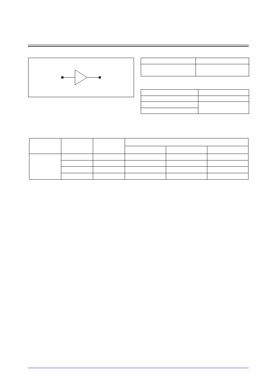
Samsung ASIC
3-207
STDL131
DL10D2_LP
10ns Delay Cell with 2X Drive
Logic Symbol
Switching Characteristics
(Typical process, 25
∞
C, 1.8V, t
R
/t
F
= 0.19ns, SL: Standard Load)
DL10D2_LP
A
Y
Path
Parameter
Delay [ns]
SL = 2
Delay Equations [ns]
Group1*
Group2*
Group3*
A to Y
tR
0.070
0.048 + 0.011*SL
0.043 + 0.012*SL
0.035 + 0.013*SL
tF
0.069
0.050 + 0.010*SL
0.049 + 0.010*SL
0.042 + 0.010*SL
tPLH
10.144
10.128 + 0.008*SL
10.134 + 0.006*SL
10.135 + 0.006*SL
tPHL
10.053
10.037 + 0.008*SL
10.044 + 0.007*SL
10.050 + 0.006*SL
*Group1 : SL < 4, *Group2 : 4 SL
<
<
=
= 12, *Group3 : 12 < SL
Truth Table
Cell Data
A
Y
0
0
1
1
Input Load (SL)
Gate Count
DL10D2_LP
DL10D2_LP
A
8.00
0.5
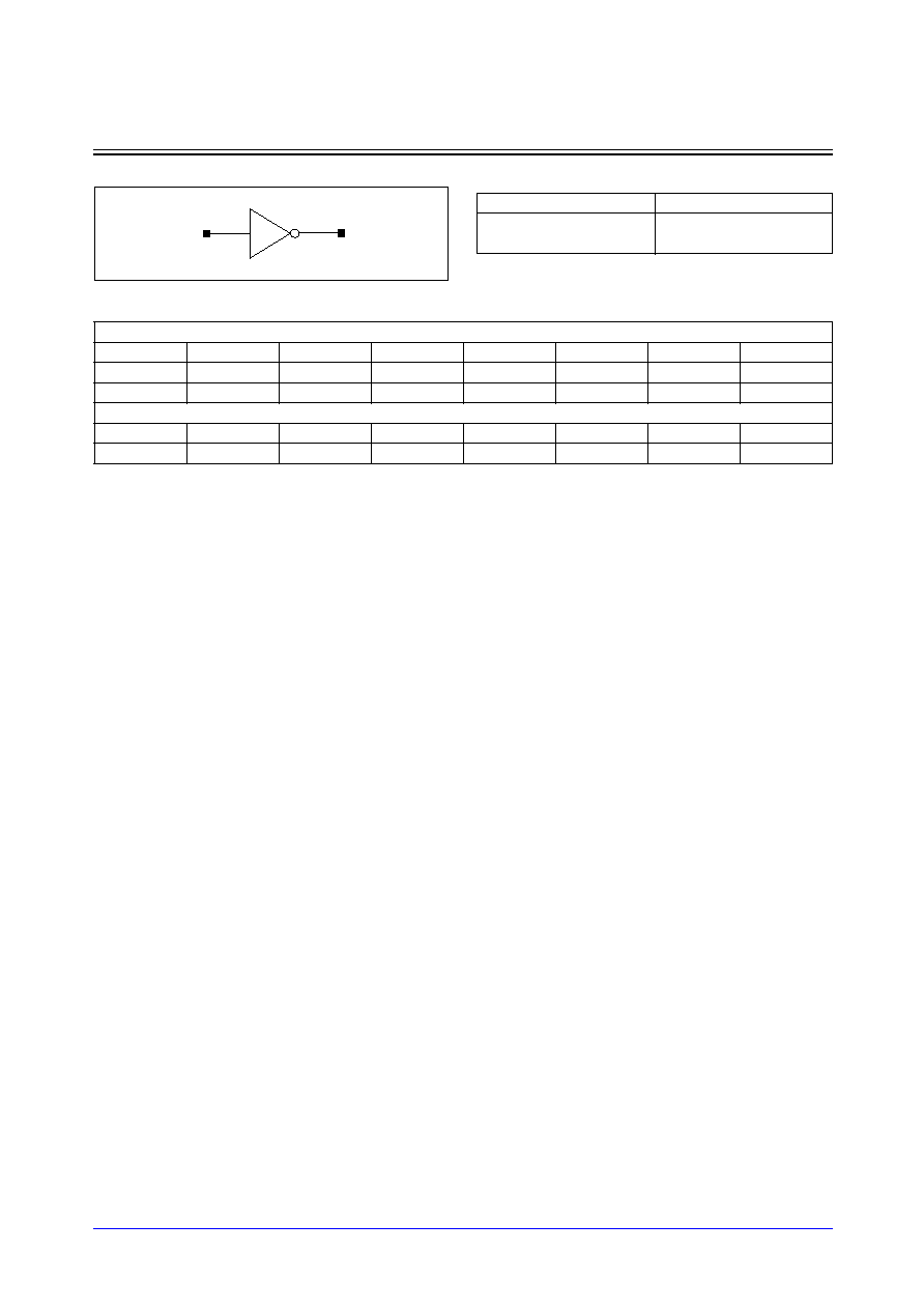
STDL131
3-208
Samsung ASIC
IV_LP/IVD2_LP/IVD3_LP/IVD4_LP/IVD6_LP/IVD8_LP/IVD16_LP/IVD24_LP
Inverter with 1X/2X/3X/4X/6X/8X/16X/24X Drive
Logic Symbol
Cell Data
Input Load (SL)
IV_LP
IVD2_LP
IVD3_LP
IVD4_LP
IVD6_LP
IVD8_LP
IVD16_LP
IVD24_LP
A
A
A
A
A
A
A
A
1.0
2.0
2.9
3.9
5.9
7.9
15.9
24.2
Gate Count
IV_LP
IVD2_LP
IVD3_LP
IVD4_LP
IVD6_LP
IVD8_LP
IVD16_LP
IVD24_LP
0.67
1.00
1.33
1.67
2.33
3.00
5.67
8.00
A
Y
Truth Table
A
Y
0
1
1
0
Samsung ASIC
3-209
STDL131
IV_LP/IVD2_LP/IVD3_LP/IVD4_LP/IVD6_LP/IVD8_LP/IVD16_LP/IVD24_LP
Inverter with 1X/2X/3X/4X/6X/8X/16X/24X Drive
Switching Characteristics
(Typical process, 25
∞
C, 1.8V, t
R
/t
F
= 0.19ns, SL: Standard Load)
IV_LP
IVD2_LP
IVD3_LP
IVD4_LP
Path
Parameter
Delay [ns]
SL = 2
Delay Equations [ns]
Group1*
Group2*
Group3*
A to Y
tR
0.112
0.069 + 0.021*SL
0.057 + 0.024*SL
0.045 + 0.026*SL
tF
0.103
0.061 + 0.021*SL
0.052 + 0.023*SL
0.042 + 0.024*SL
tPLH
0.093
0.062 + 0.015*SL
0.074 + 0.013*SL
0.074 + 0.012*SL
tPHL
0.090
0.056 + 0.017*SL
0.068 + 0.014*SL
0.068 + 0.014*SL
*Group1 : SL < 4, *Group2 : 4 SL
<
<
=
= 8, *Group3 : 8 < SL
Path
Parameter
Delay [ns]
SL = 2
Delay Equations [ns]
Group1*
Group2*
Group3*
A to Y
tR
0.085
0.064 + 0.010*SL
0.060 + 0.011*SL
0.046 + 0.013*SL
tF
0.077
0.055 + 0.011*SL
0.054 + 0.011*SL
0.042 + 0.012*SL
tPLH
0.071
0.051 + 0.010*SL
0.065 + 0.007*SL
0.071 + 0.006*SL
tPHL
0.067
0.045 + 0.011*SL
0.059 + 0.007*SL
0.065 + 0.007*SL
*Group1 : SL < 4, *Group2 : 4 SL
<
<
=
= 12, *Group3 : 12 < SL
Path
Parameter
Delay [ns]
SL = 2
Delay Equations [ns]
Group1*
Group2*
Group3*
A to Y
tR
0.079
0.064 + 0.007*SL
0.064 + 0.007*SL
0.049 + 0.008*SL
tF
0.070
0.055 + 0.008*SL
0.057 + 0.007*SL
0.043 + 0.008*SL
tPLH
0.066
0.051 + 0.008*SL
0.062 + 0.005*SL
0.072 + 0.004*SL
tPHL
0.061
0.045 + 0.008*SL
0.056 + 0.005*SL
0.066 + 0.005*SL
*Group1 : SL < 4, *Group2 : 4 SL
<
<
=
= 16, *Group3 : 16 < SL
Path
Parameter
Delay [ns]
SL = 2
Delay Equations [ns]
Group1*
Group2*
Group3*
A to Y
tR
0.073
0.061 + 0.006*SL
0.063 + 0.006*SL
0.048 + 0.006*SL
tF
0.064
0.050 + 0.007*SL
0.057 + 0.005*SL
0.043 + 0.006*SL
tPLH
0.060
0.048 + 0.006*SL
0.058 + 0.004*SL
0.071 + 0.003*SL
tPHL
0.055
0.042 + 0.007*SL
0.051 + 0.004*SL
0.065 + 0.003*SL
*Group1 : SL < 4, *Group2 : 4 SL
<
<
=
= 20, *Group3 : 20 < SL
STDL131
3-210
Samsung ASIC
IV_LP/IVD2_LP/IVD3_LP/IVD4_LP/IVD6_LP/IVD8_LP/IVD16_LP/IVD24_LP
Inverter with 1X/2X/3X/4X/6X/8X/16X/24X Drive
Switching Characteristics
(Typical process, 25
∞
C, 1.8V, t
R
/t
F
= 0.19ns, SL: Standard Load)
IVD6_LP
IVD8_LP
IVD16_LP
IVD24_LP
Path
Parameter
Delay [ns]
SL = 2
Delay Equations [ns]
Group1*
Group2*
Group3*
A to Y
tR
0.069
0.059 + 0.005*SL
0.065 + 0.004*SL
0.047 + 0.004*SL
tF
0.059
0.049 + 0.005*SL
0.056 + 0.004*SL
0.042 + 0.004*SL
tPLH
0.056
0.047 + 0.005*SL
0.055 + 0.003*SL
0.071 + 0.002*SL
tPHL
0.050
0.041 + 0.005*SL
0.048 + 0.003*SL
0.065 + 0.002*SL
*Group1 : SL < 4, *Group2 : 4 SL
<
<
=
= 29, *Group3 : 29 < SL
Path
Parameter
Delay [ns]
SL = 2
Delay Equations [ns]
Group1*
Group2*
Group3*
A to Y
tR
0.067
0.059 + 0.004*SL
0.064 + 0.003*SL
0.048 + 0.003*SL
tF
0.057
0.048 + 0.004*SL
0.055 + 0.003*SL
0.043 + 0.003*SL
tPLH
0.054
0.047 + 0.004*SL
0.053 + 0.002*SL
0.071 + 0.002*SL
tPHL
0.048
0.040 + 0.004*SL
0.046 + 0.002*SL
0.065 + 0.002*SL
*Group1 : SL < 4, *Group2 : 4 SL
<
<
=
= 37, *Group3 : 37 < SL
Path
Parameter
Delay [ns]
SL = 2
Delay Equations [ns]
Group1*
Group2*
Group3*
A to Y
tR
0.063
0.059 + 0.002*SL
0.061 + 0.001*SL
0.048 + 0.002*SL
tF
0.053
0.049 + 0.002*SL
0.052 + 0.001*SL
0.045 + 0.001*SL
tPLH
0.050
0.046 + 0.002*SL
0.050 + 0.001*SL
0.071 + 0.001*SL
tPHL
0.044
0.040 + 0.002*SL
0.043 + 0.001*SL
0.065 + 0.001*SL
*Group1 : SL < 4, *Group2 : 4 SL
<
<
=
= 71, *Group3 : 71 < SL
Path
Parameter
Delay [ns]
SL = 2
Delay Equations [ns]
Group1*
Group2*
Group3*
A to Y
tR
0.061
0.059 + 0.001*SL
0.061 + 0.001*SL
0.048 + 0.001*SL
tF
0.052
0.049 + 0.001*SL
0.051 + 0.001*SL
0.045 + 0.001*SL
tPLH
0.049
0.046 + 0.001*SL
0.049 + 0.001*SL
0.071 + 0.001*SL
tPHL
0.043
0.040 + 0.001*SL
0.042 + 0.001*SL
0.065 + 0.001*SL
*Group1 : SL < 4, *Group2 : 4 SL
<
<
=
= 104, *Group3 : 104 < SL
Samsung ASIC
3-211
STDL131
IVT_LP/IVTD2_LP/IVTD4_LP/IVTD8_LP/IVTD16_LP
Inverting Tri-State Buffer with Enable High, 1X/2X/4X/8X/16X Drive
Logic Symbol
Cell Data
Switching Characteristics
(Typical process, 25
∞
C, 1.8V, t
R
/t
F
= 0.19ns, SL: Standard Load)
IVT_LP
IVTD2_LP
Input Load (SL)
Output Load (SL)
IVT_LP
IVTD2_LP IVTD4_LP IVTD8_LP IVTD16_LP IVT_LP IVTD2_LP IVTD4_LP IVTD8_LP IVTD16_LP
A
E
A
E
A
E
A
E
A
E
Y
Y
Y
Y
Y
0.8
1.5
0.8
1.6
0.9
1.9
1.1
3.1
1.1
3.1
1.0
1.4
2.8
5.7
11.3
Gate Count
IVT_LP
IVTD2_LP
IVTD4_LP
IVTD8_LP
IVTD16_LP
3.00
3.33
4.00
6.67
9.33
A
Y
E
Path
Parameter
Delay [ns]
SL = 2
Delay Equations [ns]
Group1*
Group2*
Group3*
A to Y
tR
0.099
0.050 + 0.025*SL
0.044 + 0.026*SL
0.042 + 0.026*SL
tF
0.079
0.043 + 0.018*SL
0.047 + 0.017*SL
0.046 + 0.017*SL
tPLH
0.246
0.218 + 0.014*SL
0.224 + 0.013*SL
0.226 + 0.013*SL
tPHL
0.252
0.225 + 0.013*SL
0.234 + 0.011*SL
0.242 + 0.010*SL
E to Y
tR
0.100
0.049 + 0.025*SL
0.047 + 0.026*SL
0.042 + 0.026*SL
tF
0.077
0.042 + 0.018*SL
0.044 + 0.017*SL
0.044 + 0.017*SL
tPLH
0.164
0.136 + 0.014*SL
0.141 + 0.013*SL
0.143 + 0.013*SL
tPHL
0.205
0.179 + 0.013*SL
0.188 + 0.011*SL
0.195 + 0.010*SL
tPLZ
0.145
0.145 + 0.000*SL
0.145 + 0.000*SL
0.145 + 0.000*SL
tPHZ
0.156
0.156 + 0.000*SL
0.156 + 0.000*SL
0.156 + 0.000*SL
*Group1 : SL < 4, *Group2 : 4 SL
<
<
=
= 8, *Group3 : 8 < SL
Path
Parameter
Delay [ns]
SL = 2
Delay Equations [ns]
Group1*
Group2*
Group3*
A to Y
tR
0.072
0.046 + 0.013*SL
0.046 + 0.013*SL
0.042 + 0.013*SL
tF
0.056
0.037 + 0.010*SL
0.041 + 0.009*SL
0.043 + 0.008*SL
tPLH
0.246
0.228 + 0.009*SL
0.236 + 0.007*SL
0.244 + 0.006*SL
tPHL
0.242
0.225 + 0.008*SL
0.234 + 0.006*SL
0.246 + 0.005*SL
E to Y
tR
0.071
0.046 + 0.012*SL
0.045 + 0.013*SL
0.041 + 0.013*SL
tF
0.054
0.034 + 0.010*SL
0.038 + 0.009*SL
0.043 + 0.008*SL
tPLH
0.157
0.140 + 0.009*SL
0.147 + 0.007*SL
0.154 + 0.006*SL
tPHL
0.194
0.178 + 0.008*SL
0.186 + 0.006*SL
0.197 + 0.005*SL
tPLZ
0.158
0.158 + 0.000*SL
0.158 + 0.000*SL
0.158 + 0.000*SL
tPHZ
0.171
0.171 + 0.000*SL
0.172 + 0.000*SL
0.173 + 0.000*SL
*Group1 : SL < 4, *Group2 : 4 SL
<
<
=
= 12, *Group3 : 12 < SL
Truth Table
A
E
Y
x
0
Hi-Z
0
1
1
1
1
0
STDL131
3-212
Samsung ASIC
IVT_LP/IVTD2_LP/IVTD4_LP/IVTD8_LP/IVTD16_LP
Inverting Tri-State Buffer with Enable High, 1X/2X/4X/8X/16X Drive
Switching Characteristics
(Typical process, 25
∞
C, 1.8V, t
R
/t
F
= 0.19ns, SL: Standard Load)
IVTD4_LP
IVTD8_LP
IVTD16_LP
Path
Parameter
Delay [ns]
SL = 2
Delay Equations [ns]
Group1*
Group2*
Group3*
A to Y
tR
0.069
0.054 + 0.007*SL
0.059 + 0.006*SL
0.055 + 0.006*SL
tF
0.053
0.042 + 0.006*SL
0.047 + 0.004*SL
0.052 + 0.004*SL
tPLH
0.264
0.252 + 0.006*SL
0.260 + 0.004*SL
0.275 + 0.003*SL
tPHL
0.239
0.229 + 0.005*SL
0.235 + 0.004*SL
0.253 + 0.003*SL
E to Y
tR
0.067
0.052 + 0.008*SL
0.057 + 0.006*SL
0.056 + 0.006*SL
tF
0.050
0.037 + 0.006*SL
0.045 + 0.005*SL
0.051 + 0.004*SL
tPLH
0.173
0.162 + 0.006*SL
0.168 + 0.004*SL
0.183 + 0.003*SL
tPHL
0.191
0.181 + 0.005*SL
0.187 + 0.004*SL
0.204 + 0.003*SL
tPLZ
0.164
0.164 + 0.000*SL
0.164 + 0.000*SL
0.164 + 0.000*SL
tPHZ
0.211
0.210 + 0.000*SL
0.211 + 0.000*SL
0.212 + 0.000*SL
*Group1 : SL < 4, *Group2 : 4 SL
<
<
=
= 20, *Group3 : 20 < SL
Path
Parameter
Delay [ns]
SL = 2
Delay Equations [ns]
Group1*
Group2*
Group3*
A to Y
tR
0.060
0.053 + 0.004*SL
0.055 + 0.003*SL
0.055 + 0.003*SL
tF
0.046
0.040 + 0.003*SL
0.043 + 0.002*SL
0.051 + 0.002*SL
tPLH
0.281
0.275 + 0.003*SL
0.280 + 0.002*SL
0.297 + 0.002*SL
tPHL
0.252
0.247 + 0.003*SL
0.250 + 0.002*SL
0.268 + 0.001*SL
E to Y
tR
0.058
0.049 + 0.004*SL
0.054 + 0.003*SL
0.053 + 0.003*SL
tF
0.041
0.035 + 0.003*SL
0.038 + 0.002*SL
0.046 + 0.002*SL
tPLH
0.160
0.153 + 0.003*SL
0.158 + 0.002*SL
0.174 + 0.002*SL
tPHL
0.194
0.188 + 0.003*SL
0.192 + 0.002*SL
0.210 + 0.001*SL
tPLZ
0.178
0.178 + 0.000*SL
0.178 + 0.000*SL
0.178 + 0.000*SL
tPHZ
0.198
0.197 + 0.000*SL
0.198 + 0.000*SL
0.199 + 0.000*SL
*Group1 : SL < 4, *Group2 : 4 SL
<
<
=
= 37, *Group3 : 37 < SL
Path
Parameter
Delay [ns]
SL = 2
Delay Equations [ns]
Group1*
Group2*
Group3*
A to Y
tR
0.080
0.075 + 0.002*SL
0.078 + 0.002*SL
0.084 + 0.002*SL
tF
0.059
0.056 + 0.001*SL
0.057 + 0.001*SL
0.067 + 0.001*SL
tPLH
0.330
0.325 + 0.002*SL
0.329 + 0.001*SL
0.362 + 0.001*SL
tPHL
0.289
0.286 + 0.001*SL
0.288 + 0.001*SL
0.309 + 0.001*SL
E to Y
tR
0.075
0.070 + 0.002*SL
0.073 + 0.002*SL
0.082 + 0.002*SL
tF
0.051
0.048 + 0.002*SL
0.049 + 0.001*SL
0.066 + 0.001*SL
tPLH
0.208
0.204 + 0.002*SL
0.207 + 0.001*SL
0.238 + 0.001*SL
tPHL
0.224
0.220 + 0.002*SL
0.223 + 0.001*SL
0.249 + 0.001*SL
tPLZ
0.203
0.203 + 0.000*SL
0.203 + 0.000*SL
0.203 + 0.000*SL
tPHZ
0.291
0.290 + 0.000*SL
0.291 + 0.000*SL
0.294 + 0.000*SL
*Group1 : SL < 4, *Group2 : 4 SL
<
<
=
= 71, *Group3 : 71 < SL
Samsung ASIC
3-213
STDL131
NID_LP/NID2_LP/NID3_LP/NID4_LP/NID6_LP/NID8_LP/NID16_LP/NID24_LP
Non-Inverting Buffer with 1X/2X/3X/4X/6X/8X/16X/24X Drive
Logic Symbol
Cell Data
Input Load (SL)
NID_LP
NID2_LP
NID3_LP
NID4_LP
NID6_LP
NID8_LP
NID16_LP
NID24_LP
A
A
A
A
A
A
A
A
0.8
1.0
1.0
1.0
2.0
2.0
3.9
5.9
Gate Count
NID_LP
NID2_LP
NID3_LP
NID4_LP
NID6_LP
NID8_LP
NID16_LP
NID24_LP
1.00
1.33
1.67
2.00
3.00
3.67
7.00
10.00
A
Y
Truth Table
A
Y
0
0
1
1
STDL131
3-214
Samsung ASIC
NID_LP/NID2_LP/NID3_LP/NID4_LP/NID6_LP/NID8_LP/NID16_LP/NID24_LP
Non-Inverting Buffer with 1X/2X/3X/4X/6X/8X/16X/24X Drive
Switching Characteristics
(Typical process, 25
∞
C, 1.8V, t
R
/t
F
= 0.19ns, SL: Standard Load)
NID_LP
NID2_LP
NID3_LP
NID4_LP
Path
Parameter
Delay [ns]
SL = 2
Delay Equations [ns]
Group1*
Group2*
Group3*
A to Y
tR
0.091
0.042 + 0.024*SL
0.035 + 0.026*SL
0.033 + 0.027*SL
tF
0.074
0.035 + 0.020*SL
0.034 + 0.020*SL
0.031 + 0.020*SL
tPLH
0.144
0.117 + 0.013*SL
0.120 + 0.013*SL
0.120 + 0.013*SL
tPHL
0.150
0.125 + 0.013*SL
0.129 + 0.011*SL
0.131 + 0.011*SL
*Group1 : SL < 4, *Group2 : 4 SL
<
<
=
= 8, *Group3 : 8 < SL
Path
Parameter
Delay [ns]
SL = 2
Delay Equations [ns]
Group1*
Group2*
Group3*
A to Y
tR
0.067
0.044 + 0.011*SL
0.038 + 0.013*SL
0.032 + 0.013*SL
tF
0.054
0.034 + 0.010*SL
0.034 + 0.010*SL
0.031 + 0.010*SL
tPLH
0.142
0.127 + 0.008*SL
0.132 + 0.007*SL
0.135 + 0.006*SL
tPHL
0.148
0.133 + 0.008*SL
0.139 + 0.006*SL
0.145 + 0.006*SL
*Group1 : SL < 4, *Group2 : 4 SL
<
<
=
= 12, *Group3 : 12 < SL
Path
Parameter
Delay [ns]
SL = 2
Delay Equations [ns]
Group1*
Group2*
Group3*
A to Y
tR
0.066
0.049 + 0.008*SL
0.050 + 0.008*SL
0.042 + 0.009*SL
tF
0.056
0.041 + 0.007*SL
0.045 + 0.006*SL
0.040 + 0.007*SL
tPLH
0.155
0.143 + 0.006*SL
0.148 + 0.005*SL
0.154 + 0.004*SL
tPHL
0.161
0.149 + 0.006*SL
0.155 + 0.004*SL
0.164 + 0.004*SL
*Group1 : SL < 4, *Group2 : 4 SL
<
<
=
= 16, *Group3 : 16 < SL
Path
Parameter
Delay [ns]
SL = 2
Delay Equations [ns]
Group1*
Group2*
Group3*
A to Y
tR
0.066
0.053 + 0.006*SL
0.055 + 0.006*SL
0.048 + 0.006*SL
tF
0.056
0.046 + 0.005*SL
0.046 + 0.005*SL
0.046 + 0.005*SL
tPLH
0.169
0.159 + 0.005*SL
0.165 + 0.004*SL
0.176 + 0.003*SL
tPHL
0.174
0.164 + 0.005*SL
0.170 + 0.004*SL
0.183 + 0.003*SL
*Group1 : SL < 4, *Group2 : 4 SL
<
<
=
= 20, *Group3 : 20 < SL
Samsung ASIC
3-215
STDL131
NID_LP/NID2_LP/NID3_LP/NID4_LP/NID6_LP/NID8_LP/NID16_LP/NID24_LP
Non-Inverting Buffer with 1X/2X/3X/4X/6X/8X/16X/24X Drive
Switching Characteristics
(Typical process, 25
∞
C, 1.8V, t
R
/t
F
= 0.19ns, SL: Standard Load)
NID6_LP
NID8_LP
NID16_LP
NID24_LP
Path
Parameter
Delay [ns]
SL = 2
Delay Equations [ns]
Group1*
Group2*
Group3*
A to Y
tR
0.053
0.043 + 0.005*SL
0.047 + 0.004*SL
0.039 + 0.004*SL
tF
0.045
0.038 + 0.004*SL
0.040 + 0.003*SL
0.037 + 0.003*SL
tPLH
0.143
0.137 + 0.003*SL
0.140 + 0.002*SL
0.149 + 0.002*SL
tPHL
0.149
0.143 + 0.003*SL
0.147 + 0.002*SL
0.157 + 0.002*SL
*Group1 : SL < 4, *Group2 : 4 SL
<
<
=
= 29, *Group3 : 29 < SL
Path
Parameter
Delay [ns]
SL = 2
Delay Equations [ns]
Group1*
Group2*
Group3*
A to Y
tR
0.058
0.052 + 0.003*SL
0.052 + 0.003*SL
0.046 + 0.003*SL
tF
0.051
0.046 + 0.003*SL
0.047 + 0.002*SL
0.045 + 0.002*SL
tPLH
0.160
0.154 + 0.003*SL
0.158 + 0.002*SL
0.170 + 0.002*SL
tPHL
0.165
0.160 + 0.003*SL
0.163 + 0.002*SL
0.177 + 0.001*SL
*Group1 : SL < 4, *Group2 : 4 SL
<
<
=
= 37, *Group3 : 37 < SL
Path
Parameter
Delay [ns]
SL = 2
Delay Equations [ns]
Group1*
Group2*
Group3*
A to Y
tR
0.055
0.053 + 0.001*SL
0.051 + 0.002*SL
0.046 + 0.002*SL
tF
0.048
0.046 + 0.001*SL
0.046 + 0.001*SL
0.046 + 0.001*SL
tPLH
0.157
0.154 + 0.002*SL
0.156 + 0.001*SL
0.170 + 0.001*SL
tPHL
0.162
0.159 + 0.001*SL
0.161 + 0.001*SL
0.177 + 0.001*SL
*Group1 : SL < 4, *Group2 : 4 SL
<
<
=
= 71, *Group3 : 71 < SL
Path
Parameter
Delay [ns]
SL = 2
Delay Equations [ns]
Group1*
Group2*
Group3*
A to Y
tR
0.054
0.053 + 0.001*SL
0.052 + 0.001*SL
0.046 + 0.001*SL
tF
0.047
0.045 + 0.001*SL
0.046 + 0.001*SL
0.046 + 0.001*SL
tPLH
0.156
0.154 + 0.001*SL
0.155 + 0.001*SL
0.170 + 0.001*SL
tPHL
0.161
0.159 + 0.001*SL
0.161 + 0.001*SL
0.177 + 0.000*SL
*Group1 : SL < 4, *Group2 : 4 SL
<
<
=
= 104, *Group3 : 104 < SL
STDL131
3-216
Samsung ASIC
NIT_LP/NITD2_LP/NITD4_LP/NITD8_LP/NITD16_LP
Non-Inverting Tri-State Buffer with Enable High, 1X/2X/4X/8X/16X Drive
Logic Symbol
Cell Data
Input Load (SL)
Output Load (SL)
NIT_LP
NITD2_LP NITD4_LP
NITD8_LP NITD16_LP NIT_LP NITD2_LP NITD4_LP NITD8_LP NITD16_LP
A
E
A
E
A
E
A
E
A
E
Y
Y
Y
Y
Y
1.4
1.5
1.7
1.6
1.9
1.8
4.2
3.2
4.1
3.2
1.0
1.4
2.8
5.6
11.1
Gate Count
NIT_LP
NITD2_LP
NITD4_LP
NITD8_LP
NITD16_LP
2.67
3.00
3.67
6.00
8.67
A
Y
E
Truth Table
A
E
Y
x
0
Hi-Z
0
1
0
1
1
1
Samsung ASIC
3-217
STDL131
NIT_LP/NITD2_LP/NITD4_LP/NITD8_LP/NITD16_LP
Non-Inverting Tri-State Buffer with Enable High, 1X/2X/4X/8X/16X Drive
Switching Characteristics
(Typical process, 25
∞
C, 1.8V, t
R
/t
F
= 0.19ns, SL: Standard Load)
NIT_LP
NITD2_LP
NITD4_LP
Path
Parameter
Delay [ns]
SL = 2
Delay Equations [ns]
Group1*
Group2*
Group3*
A to Y
tR
0.098
0.048 + 0.025*SL
0.045 + 0.026*SL
0.040 + 0.026*SL
tF
0.077
0.042 + 0.018*SL
0.045 + 0.017*SL
0.043 + 0.017*SL
tPLH
0.155
0.127 + 0.014*SL
0.132 + 0.013*SL
0.134 + 0.013*SL
tPHL
0.192
0.165 + 0.013*SL
0.174 + 0.011*SL
0.182 + 0.010*SL
E to Y
tR
0.096
0.045 + 0.026*SL
0.044 + 0.026*SL
0.039 + 0.026*SL
tF
0.076
0.040 + 0.018*SL
0.043 + 0.017*SL
0.043 + 0.017*SL
tPLH
0.158
0.130 + 0.014*SL
0.135 + 0.013*SL
0.137 + 0.012*SL
tPHL
0.202
0.176 + 0.013*SL
0.184 + 0.011*SL
0.191 + 0.010*SL
tPLZ
0.145
0.145 + 0.000*SL
0.145 + 0.000*SL
0.145 + 0.000*SL
tPHZ
0.149
0.149 + 0.000*SL
0.150 + 0.000*SL
0.150 + 0.000*SL
*Group1 : SL < 4, *Group2 : 4 SL
<
<
=
= 8, *Group3 : 8 < SL
Path
Parameter
Delay [ns]
SL = 2
Delay Equations [ns]
Group1*
Group2*
Group3*
A to Y
tR
0.072
0.045 + 0.013*SL
0.048 + 0.012*SL
0.040 + 0.013*SL
tF
0.057
0.036 + 0.010*SL
0.044 + 0.008*SL
0.044 + 0.008*SL
tPLH
0.149
0.132 + 0.009*SL
0.139 + 0.007*SL
0.146 + 0.006*SL
tPHL
0.179
0.163 + 0.008*SL
0.171 + 0.006*SL
0.183 + 0.005*SL
E to Y
tR
0.070
0.045 + 0.012*SL
0.044 + 0.013*SL
0.040 + 0.013*SL
tF
0.055
0.035 + 0.010*SL
0.039 + 0.009*SL
0.044 + 0.008*SL
tPLH
0.154
0.137 + 0.009*SL
0.144 + 0.007*SL
0.150 + 0.006*SL
tPHL
0.194
0.178 + 0.008*SL
0.186 + 0.006*SL
0.198 + 0.005*SL
tPLZ
0.157
0.157 + 0.000*SL
0.157 + 0.000*SL
0.157 + 0.000*SL
tPHZ
0.168
0.168 + 0.000*SL
0.169 + 0.000*SL
0.169 + 0.000*SL
*Group1 : SL < 4, *Group2 : 4 SL
<
<
=
= 12, *Group3 : 12 < SL
Path
Parameter
Delay [ns]
SL = 2
Delay Equations [ns]
Group1*
Group2*
Group3*
A to Y
tR
0.070
0.057 + 0.007*SL
0.058 + 0.006*SL
0.054 + 0.006*SL
tF
0.054
0.044 + 0.005*SL
0.046 + 0.005*SL
0.053 + 0.004*SL
tPLH
0.165
0.154 + 0.006*SL
0.161 + 0.004*SL
0.176 + 0.003*SL
tPHL
0.185
0.175 + 0.005*SL
0.181 + 0.004*SL
0.198 + 0.003*SL
E to Y
tR
0.066
0.051 + 0.008*SL
0.056 + 0.006*SL
0.053 + 0.006*SL
tF
0.049
0.037 + 0.006*SL
0.044 + 0.005*SL
0.050 + 0.004*SL
tPLH
0.170
0.159 + 0.006*SL
0.166 + 0.004*SL
0.180 + 0.003*SL
tPHL
0.194
0.184 + 0.005*SL
0.190 + 0.004*SL
0.207 + 0.003*SL
tPLZ
0.165
0.165 + 0.000*SL
0.166 + 0.000*SL
0.166 + 0.000*SL
tPHZ
0.207
0.206 + 0.000*SL
0.207 + 0.000*SL
0.208 + 0.000*SL
*Group1 : SL < 4, *Group2 : 4 SL
<
<
=
= 20, *Group3 : 20 < SL
STDL131
3-218
Samsung ASIC
NIT_LP/NITD2_LP/NITD4_LP/NITD8_LP/NITD16_LP
Non-Inverting Tri-State Buffer with Enable High, 1X/2X/4X/8X/16X Drive
Switching Characteristics
(Typical process, 25
∞
C, 1.8V, t
R
/t
F
= 0.19ns, SL: Standard Load)
NITD8_LP
NITD16_LP
Path
Parameter
Delay [ns]
SL = 2
Delay Equations [ns]
Group1*
Group2*
Group3*
A to Y
tR
0.061
0.053 + 0.004*SL
0.057 + 0.003*SL
0.055 + 0.003*SL
tF
0.046
0.040 + 0.003*SL
0.043 + 0.002*SL
0.048 + 0.002*SL
tPLH
0.154
0.147 + 0.003*SL
0.152 + 0.002*SL
0.169 + 0.002*SL
tPHL
0.172
0.166 + 0.003*SL
0.170 + 0.002*SL
0.188 + 0.001*SL
E to Y
tR
0.058
0.051 + 0.004*SL
0.053 + 0.003*SL
0.052 + 0.003*SL
tF
0.040
0.034 + 0.003*SL
0.037 + 0.002*SL
0.046 + 0.002*SL
tPLH
0.160
0.154 + 0.003*SL
0.158 + 0.002*SL
0.174 + 0.002*SL
tPHL
0.192
0.187 + 0.003*SL
0.191 + 0.002*SL
0.208 + 0.001*SL
tPLZ
0.179
0.179 + 0.000*SL
0.179 + 0.000*SL
0.179 + 0.000*SL
tPHZ
0.196
0.196 + 0.000*SL
0.197 + 0.000*SL
0.198 + 0.000*SL
*Group1 : SL < 4, *Group2 : 4 SL
<
<
=
= 37, *Group3 : 37 < SL
Path
Parameter
Delay [ns]
SL = 2
Delay Equations [ns]
Group1*
Group2*
Group3*
A to Y
tR
0.078
0.074 + 0.002*SL
0.075 + 0.002*SL
0.086 + 0.002*SL
tF
0.060
0.057 + 0.001*SL
0.058 + 0.001*SL
0.067 + 0.001*SL
tPLH
0.202
0.198 + 0.002*SL
0.202 + 0.001*SL
0.235 + 0.001*SL
tPHL
0.207
0.204 + 0.002*SL
0.206 + 0.001*SL
0.227 + 0.001*SL
E to Y
tR
0.075
0.070 + 0.002*SL
0.072 + 0.002*SL
0.085 + 0.002*SL
tF
0.050
0.047 + 0.002*SL
0.049 + 0.001*SL
0.065 + 0.001*SL
tPLH
0.209
0.205 + 0.002*SL
0.209 + 0.001*SL
0.240 + 0.001*SL
tPHL
0.221
0.218 + 0.002*SL
0.220 + 0.001*SL
0.246 + 0.001*SL
tPLZ
0.205
0.205 + 0.000*SL
0.205 + 0.000*SL
0.205 + 0.000*SL
tPHZ
0.295
0.294 + 0.000*SL
0.295 + 0.000*SL
0.298 + 0.000*SL
*Group1 : SL < 4, *Group2 : 4 SL
<
<
=
= 71, *Group3 : 71 < SL
Samsung ASIC
3-219
STDL131
FLIP-FLOPS
Cell List
Cell Name
Function Description
FD1_LP
D Flip-Flop with 1X Drive
FD1D2_LP
D Flip-Flop with 2X Drive
FD1S_LP
D Flip-Flop with Scan, 1X Drive
FD1SD2_LP
D Flip-Flop with Scan, 2X Drive
FD1SQ_LP
D Flip-Flop with Scan, Q Output Only, 1X Drive
FD1SQD2_LP
D Flip-Flop with Scan, Q Output Only, 2X Drive
FD1Q_LP
D Flip-Flop with Q Output Only, 1X Drive
FD1QD2_LP
D Flip-Flop with Q Output Only, 2X Drive
FD2_LP
D Flip-Flop with Reset, 1X Drive
FD2D2_LP
D Flip-Flop with Reset, 2X Drive
FD2S_LP
D Flip-Flop with Reset, Scan, 1X Drive
FD2SD2_LP
D Flip-Flop with Reset, Scan, 2X Drive
FD2SQ_LP
D Flip-Flop with Reset, Scan, Q Output Only, 1X Drive
FD2SQD2_LP
D Flip-Flop with Reset, Scan, Q Output Only, 2X Drive
FD2Q_LP
D Flip-Flop with Reset, Q Output Only, 1X Drive
FD2QD2_LP
D Flip-Flop with Reset, Q Output Only, 2X Drive
FD3_LP
D Flip-Flop with Set, 1X Drive
FD3D2_LP
D Flip-Flop with Set, 2X Drive
FD3S_LP
D Flip-Flop with Set, Scan, 1X Drive
FD3SD2_LP
D Flip-Flop with Set, Scan, 2X Drive
FD3SQ_LP
D Flip-Flop with Set, Scan, Q Output Only, 1X Drive
FD3SQD2_LP
D Flip-Flop with Set, Scan, Q Output Only, 2X Drive
FD3Q_LP
D Flip-Flop with Set, Q Output Only, 1X Drive
FD3QD2_LP
D Flip-Flop with Set, Q Output Only, 2X Drive
FD4_LP
D Flip-Flop with Reset, Se, 1X Drive
FD4D2_LP
D Flip-Flop with Reset, Set, 2X Drive
FD4S_LP
D Flip-Flop with Reset, Set, Scan, 1X Drive
FD4SD2_LP
D Flip-Flop with Reset, Set, Scan, 2X Drive
FD4SQ_LP
D Flip-Flop with Reset, Set, Scan, Q Output Only, 1X Drive
FD4SQD2_LP
D Flip-Flop with Reset, Set, Scan, Q Output Only, 2X Drive
FD4Q_LP
D Flip-Flop with Reset, Set, Q Output Only, 1X Drive
FD4QD2_LP
D Flip-Flop with Reset, Set, Q Output Only, 2X Drive
FD5_LP
D Flip-Flop with Negative Edge Trigger, 1X Drive
FD5D2_LP
D Flip-Flop with Negative Edge Trigger, 2X Drive
FD5S_LP
D Flip-Flop with Negative Edge Trigger, Scan, 1X Drive
FD5SD2_LP
D Flip-Flop with Negative Edge Trigger, Scan, 2X Drive
FD6_LP
D Flip-Flop with Negative Edge Trigger, Reset, 1X Drive
FD6D2_LP
D Flip-Flop with Negative Edge Trigger, Reset, 2X Drive
STDL131
3-220
Samsung ASIC
FLIP-FLOPS
Cell List (Continued)
FD6S_LP
D Flip-Flop with Negative Edge Trigger, Reset, Scan, 1X Drive
FD6SD2_LP
D Flip-Flop with Negative Edge Trigger, Reset, Scan, 2X Drive
FD7_LP
D Flip-Flop with Negative Edge Trigger, Set, 1X Drive
FD7D2_LP
D Flip-Flop with Negative Edge Trigger, Set, 2X Drive
FD7S_LP
D Flip-Flop with Negative Edge Trigger, Set, Scan, 1X Drive
FD7SD2_LP
D Flip-Flop with Negative Edge Trigger, Set, Scan, 2X Drive
FD8_LP
D Flip-Flop with Negative Edge Trigger, Reset, Set, 1X Drive
FD8D2_LP
D Flip-Flop with Negative Edge Trigger, Reset, Set, 2X Drive
FD8S_LP
D Flip-Flop with Negative Edge Trigger, Reset, Set, Scan, 1X Drive
FD8SD2_LP
D Flip-Flop with Negative Edge Trigger, Reset, Set, Scan, 2X Drive
FDS2_LP
D Flip-Flop with Synchronous Clear, 1X Drive
FDS2D2_LP
D Flip-Flop with Synchronous Clear, 2X Drive
FDS2S_LP
D Flip-Flop with Synchronous Clear, Scan, 1X Drive
FDS2SD2_LP
D Flip-Flop with Synchronous Clear, Scan, 2X Drive
FDS3_LP
D Flip-Flop with Synchronous Set, 1X Drive
FDS3D2_LP
D Flip-Flop with Synchronous Set, 2X Drive
FDS3S_LP
Flip-Flop with Synchronous Set, Scan, 1X Drive
FDS3SD2_LP
Flip-Flop with Synchronous Set, Scan, 2x Drive
FJ2_LP
JK Flip-Flop with Reset, 1X Drive
FJ2D2_LP
JK Flip-Flop with Reset, 2X Drive
FJ2S_LP
JK Flip-Flop with Reset, Scan, 1X Drive
FJ2SD2_LP
JK Flip-Flop with Reset, Scan, 2X Drive
FJ4_LP
JK Flip-Flop with Reset, Set, 1X Drive
FJ4D2_LP
JK Flip-Flop with Reset, Set, 2X Drive
FJ4S_LP
JK Flip-Flop with Reset, Set, Scan, 1X Drive
FJ4SD2_LP
JK Flip-Flop with Reset, Set, Scan, 2X Drive
FT2_LP
Toggle Flip-Flop with Reset, 1X Drive
FT2D2_LP
Toggle Flip-Flop with Reset, 2X Drive
Cell Name
Function Description
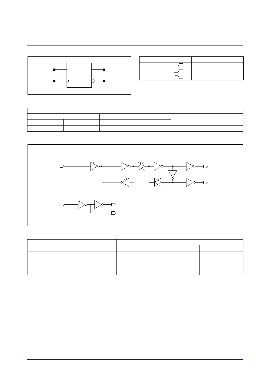
Samsung ASIC
3-221
STDL131
FD1_LP/FD1D2_LP
D Flip-Flop with 1X/2X Drive
Logic Symbol
Cell Data
Schematic Diagram
Timing Requirements
(Typical process, 25
∞
C, 1.8V, Unit = ns)
Input Load (SL)
Gate Count
FD1_LP
FD1D2_LP
FD1_LP
FD1D2_LP
D
CK
D
CK
0.7
1.1
0.7
1.1
5.67
6.00
Parameter
Symbol
Value (ns)
FD1_LP
FD1D2_LP
Input Setup Time (D to CK)
t
SU
0.135
0.132
Input Hold Time (D to CK)
t
HD
0.010
0.010
Pulse Width Low (CK)
t
PWL
0.214
0.217
Pulse Width High (CK)
t
PWH
0.155
0.168
D
CK
Q
QN
CL
CLB
Q
CLB
CL
QN
D
CK
CL
CLB
CLB
CL
CL
CLB
Truth Table
D
CK
Q (n+1)
QN (n+1)
0
0
1
1
1
0
x
Q (n)
QN (n)
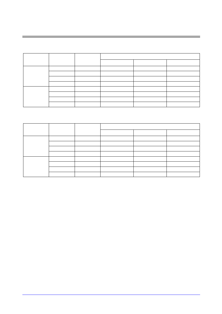
STDL131
3-222
Samsung ASIC
FD1_LP/FD1D2_LP
D Flip-Flop with 1X/2X Drive
Switching Characteristics
(Typical process, 25
∞
C, 1.8V, t
R
/t
F
= 0.19ns, SL: Standard Load)
FD1_LP
FD1D2_LP
Path
Parameter
Delay [ns]
SL = 2
Delay Equations [ns]
Group1*
Group2*
Group3*
CK to Q
tR
0.095
0.044 + 0.025*SL
0.041 + 0.026*SL
0.037 + 0.027*SL
tF
0.072
0.037 + 0.017*SL
0.037 + 0.017*SL
0.037 + 0.017*SL
tPLH
0.298
0.271 + 0.014*SL
0.274 + 0.013*SL
0.275 + 0.013*SL
tPHL
0.294
0.271 + 0.012*SL
0.277 + 0.010*SL
0.281 + 0.010*SL
CK to QN
tR
0.090
0.039 + 0.026*SL
0.035 + 0.027*SL
0.033 + 0.027*SL
tF
0.069
0.036 + 0.017*SL
0.034 + 0.017*SL
0.032 + 0.017*SL
tPLH
0.351
0.325 + 0.013*SL
0.327 + 0.013*SL
0.328 + 0.013*SL
tPHL
0.352
0.329 + 0.011*SL
0.334 + 0.010*SL
0.337 + 0.010*SL
*Group1 : SL < 4, *Group2 : 4 SL
<
<
=
= 8, *Group3 : 8 < SL
Path
Parameter
Delay [ns]
SL = 2
Delay Equations [ns]
Group1*
Group2*
Group3*
CK to Q
tR
0.068
0.044 + 0.012*SL
0.041 + 0.013*SL
0.036 + 0.013*SL
tF
0.057
0.039 + 0.009*SL
0.040 + 0.008*SL
0.041 + 0.008*SL
tPLH
0.301
0.284 + 0.008*SL
0.290 + 0.007*SL
0.294 + 0.006*SL
tPHL
0.300
0.285 + 0.008*SL
0.292 + 0.006*SL
0.302 + 0.005*SL
CK to QN
tR
0.063
0.038 + 0.012*SL
0.036 + 0.013*SL
0.030 + 0.013*SL
tF
0.052
0.035 + 0.008*SL
0.034 + 0.008*SL
0.033 + 0.009*SL
tPLH
0.376
0.361 + 0.007*SL
0.365 + 0.006*SL
0.368 + 0.006*SL
tPHL
0.374
0.361 + 0.007*SL
0.367 + 0.005*SL
0.373 + 0.005*SL
*Group1 : SL < 4, *Group2 : 4 SL
<
<
=
= 12, *Group3 : 12 < SL
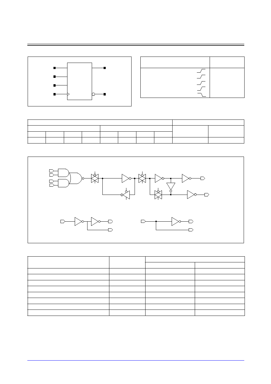
Samsung ASIC
3-223
STDL131
FD1S_LP/FD1SD2_LP
D Flip-Flop with Scan, 1X/2X Drive
Logic Symbol
Cell Data
Schematic Diagram
Timing Requirements
(Typical process, 25
∞
C, 1.8V, Unit = ns)
Input Load (SL)
Gate Count
FD1S_LP
FD1SD2_LP
FD1S_LP
FD1SD2_LP
D
CK
TI
TE
D
CK
TI
TE
0.7
1.1
0.7
1.7
0.7
1.1
0.7
1.6
7.67
7.67
Parameter
Symbol
Value (ns)
FD1S_LP
FD1SD2_LP
Input Setup Time (D to CK)
t
SU
0.275
0.272
Input Hold Time (D to CK)
t
HD
0.010
0.010
Input Setup Time (TI to CK)
t
SU
0.339
0.336
Input Hold Time (TI to CK)
t
HD
0.010
0.010
Input Setup Time (TE to CK)
t
SU
0.327
0.324
Input Hold Time (TE to CK)
t
HD
0.010
0.010
Pulse Width Low (CK)
t
PWL
0.312
0.310
Pulse Width High (CK)
t
PWH
0.160
0.169
Q
QN
D
TI
TE
CK
CL
CLB
Q
CLB
CL
QN
D
CK
CL
CLB
TE
TI
TE
TEB
TE
CLB
CL
CL
CLB
TEB
Truth Table
D
TI
TE
CK
Q
(n+1)
QN
(n+1)
0
x
0
0
1
1
x
0
1
0
x
0
1
0
1
x
1
1
1
0
x
x
x
Q(n)
QN(n)

STDL131
3-224
Samsung ASIC
FD1S_LP/FD1SD2_LP
D Flip-Flop with Scan, 1X/2X Drive
Switching Characteristics
(Typical process, 25
∞
C, 1.8V, t
R
/t
F
= 0.19ns, SL: Standard Load)
FD1S_LP
FD1SD2_LP
Path
Parameter
Delay [ns]
SL = 2
Delay Equations [ns]
Group1*
Group2*
Group3*
CK to Q
tR
0.095
0.044 + 0.025*SL
0.040 + 0.026*SL
0.037 + 0.027*SL
tF
0.072
0.037 + 0.017*SL
0.038 + 0.017*SL
0.036 + 0.017*SL
tPLH
0.303
0.276 + 0.013*SL
0.279 + 0.013*SL
0.280 + 0.013*SL
tPHL
0.299
0.276 + 0.012*SL
0.282 + 0.010*SL
0.286 + 0.010*SL
CK to QN
tR
0.090
0.040 + 0.025*SL
0.034 + 0.027*SL
0.033 + 0.027*SL
tF
0.069
0.036 + 0.017*SL
0.036 + 0.017*SL
0.030 + 0.017*SL
tPLH
0.358
0.332 + 0.013*SL
0.334 + 0.013*SL
0.335 + 0.013*SL
tPHL
0.359
0.337 + 0.011*SL
0.342 + 0.010*SL
0.345 + 0.010*SL
*Group1 : SL < 4, *Group2 : 4 SL
<
<
=
= 8, *Group3 : 8 < SL
Path
Parameter
Delay [ns]
SL = 2
Delay Equations [ns]
Group1*
Group2*
Group3*
CK to Q
tR
0.069
0.045 + 0.012*SL
0.042 + 0.013*SL
0.036 + 0.013*SL
tF
0.057
0.040 + 0.009*SL
0.041 + 0.008*SL
0.041 + 0.008*SL
tPLH
0.302
0.286 + 0.008*SL
0.291 + 0.007*SL
0.295 + 0.006*SL
tPHL
0.305
0.289 + 0.008*SL
0.297 + 0.006*SL
0.306 + 0.005*SL
CK to QN
tR
0.064
0.039 + 0.012*SL
0.037 + 0.013*SL
0.031 + 0.013*SL
tF
0.053
0.036 + 0.009*SL
0.038 + 0.008*SL
0.034 + 0.009*SL
tPLH
0.382
0.367 + 0.007*SL
0.371 + 0.006*SL
0.373 + 0.006*SL
tPHL
0.377
0.363 + 0.007*SL
0.369 + 0.005*SL
0.376 + 0.005*SL
*Group1 : SL < 4, *Group2 : 4 SL
<
<
=
= 12, *Group3 : 12 < SL
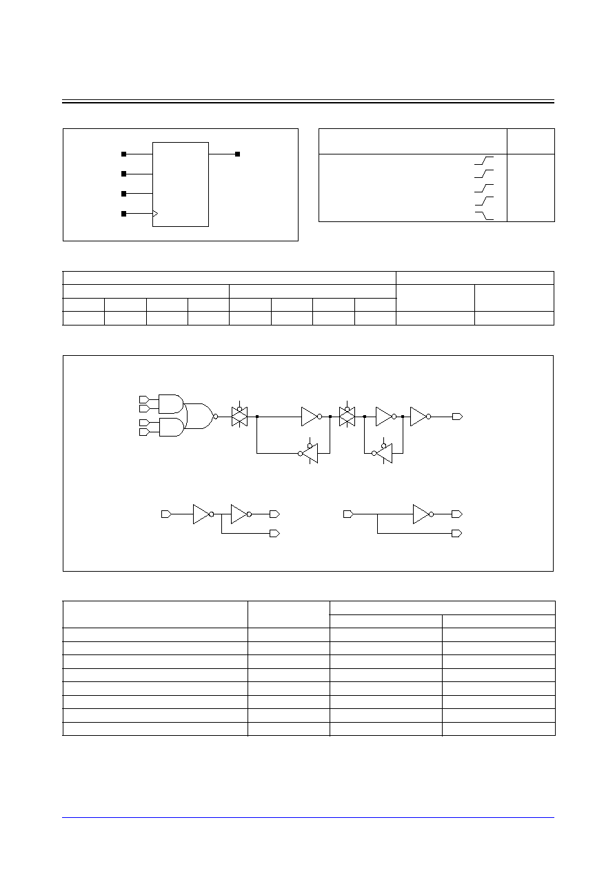
Samsung ASIC
3-225
STDL131
FD1SQ_LP/FD1SQD2_LP
D Flip-Flop with Scan, Q Output Only, 1X/2X Drive
Logic Symbol
Cell Data
Schematic Diagram
Timing Requirements
(Typical process, 25
∞
C, 1.8V, Unit = ns)
Input Load (SL)
Gate Count
FD1SQ_LP
FD1SQD2_LP
FD1SQ_LP
FD1SQD2_LP
D
CK
TI
TE
D
CK
TI
TE
0.7
1.1
0.7
1.7
0.7
1.1
0.7
1.6
6.67
7.00
Parameter
Symbol
Value (ns)
FD1SQ_LP
FD1SQD2_LP
Input Setup Time (D to CK)
t
SU
0.275
0.271
Input Hold Time (D to CK)
t
HD
0.010
0.010
Input Setup Time (TI to CK)
t
SU
0.337
0.334
Input Hold Time (TI to CK)
t
HD
0.010
0.010
Input Setup Time (TE to CK)
t
SU
0.325
0.323
Input Hold Time (TE to CK)
t
HD
0.010
0.010
Pulse Width Low (CK)
t
PWL
0.310
0.310
Pulse Width High (CK)
t
PWH
0.138
0.146
Q
D
TI
TE
CK
CL
CLB
Q
CLB
CL
CLB
CL
CL
CLB
CK
CL
CLB
TE
TEB
TE
D
TE
TI
TEB
Truth Table
D
TI
TE
CK
Q
(n+1)
0
x
0
0
1
x
0
1
x
0
1
0
x
1
1
1
x
x
x
Q(n)
STDL131
3-226
Samsung ASIC
FD1SQ_LP/FD1SQD2_LP
D Flip-Flop with Scan, Q Output Only, 1X/2X Drive
Switching Characteristics
(Typical process, 25
∞
C, 1.8V, t
R
/t
F
= 0.19ns, SL: Standard Load)
FD1SQ_LP
FD1SQD2_LP
Path
Parameter
Delay [ns]
SL = 2
Delay Equations [ns]
Group1*
Group2*
Group3*
CK to Q
tR
0.093
0.042 + 0.025*SL
0.038 + 0.026*SL
0.035 + 0.027*SL
tF
0.068
0.034 + 0.017*SL
0.034 + 0.017*SL
0.030 + 0.018*SL
tPLH
0.286
0.260 + 0.013*SL
0.262 + 0.013*SL
0.263 + 0.013*SL
tPHL
0.285
0.263 + 0.011*SL
0.267 + 0.010*SL
0.270 + 0.010*SL
*Group1 : SL < 4, *Group2 : 4 SL
<
<
=
= 8, *Group3 : 8 < SL
Path
Parameter
Delay [ns]
SL = 2
Delay Equations [ns]
Group1*
Group2*
Group3*
CK to Q
tR
0.066
0.043 + 0.011*SL
0.039 + 0.013*SL
0.032 + 0.013*SL
tF
0.052
0.034 + 0.009*SL
0.037 + 0.008*SL
0.034 + 0.009*SL
tPLH
0.290
0.275 + 0.008*SL
0.279 + 0.007*SL
0.282 + 0.006*SL
tPHL
0.291
0.277 + 0.007*SL
0.283 + 0.005*SL
0.290 + 0.005*SL
*Group1 : SL < 4, *Group2 : 4 SL
<
<
=
= 12, *Group3 : 12 < SL
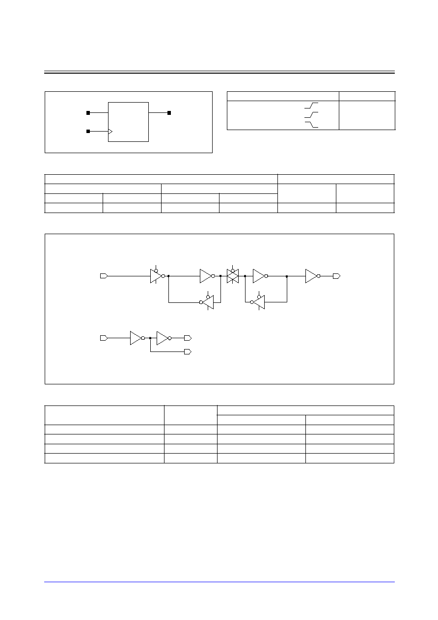
Samsung ASIC
3-227
STDL131
FD1Q_LP/FD1QD2_LP
D Flip-Flop with Q Output Only, 1X/2X Drive
Logic Symbol
Cell Data
Schematic Diagram
Timing Requirements
(Typical process, 25
∞
C, 1.8V, Unit = ns)
Input Load (SL)
Gate Count
FD1Q_LP
FD1QD2_LP
FD1Q_LP
FD1QD2_LP
D
CK
D
CK
0.7
1.1
0.7
1.1
4.67
5.00
Parameter
Symbol
Value (ns)
FD1Q_LP
FD1QD2_LP
Input Setup Time (D to CK)
t
SU
0.130
0.128
Input Hold Time (D to CK)
t
HD
0.010
0.010
Pulse Width Low (CK)
t
PWL
0.216
0.215
Pulse Width High (CK)
t
PWH
0.139
0.146
D
CK
Q
CL
CLB
Q
CLB
CL
CL
CLB
D
CK
CL
CLB
CL
CLB
Truth Table
D
CK
Q (n+1)
0
0
1
1
x
Q (n)

STDL131
3-228
Samsung ASIC
FD1Q_LP/FD1QD2_LP
D Flip-Flop with Q Output Only, 1X/2X Drive
Switching Characteristics
(Typical process, 25
∞
C, 1.8V, t
R
/t
F
= 0.19ns, SL: Standard Load)
FD1Q_LP
FD1QD2_LP
Path
Parameter
Delay [ns]
SL = 2
Delay Equations [ns]
Group1*
Group2*
Group3*
CK to Q
tR
0.092
0.042 + 0.025*SL
0.038 + 0.026*SL
0.033 + 0.027*SL
tF
0.067
0.033 + 0.017*SL
0.033 + 0.017*SL
0.028 + 0.018*SL
tPLH
0.286
0.259 + 0.013*SL
0.261 + 0.013*SL
0.262 + 0.013*SL
tPHL
0.280
0.258 + 0.011*SL
0.263 + 0.010*SL
0.265 + 0.010*SL
*Group1 : SL < 4, *Group2 : 4 SL
<
<
=
= 8, *Group3 : 8 < SL
Path
Parameter
Delay [ns]
SL = 2
Delay Equations [ns]
Group1*
Group2*
Group3*
CK to Q
tR
0.066
0.043 + 0.012*SL
0.039 + 0.013*SL
0.032 + 0.013*SL
tF
0.052
0.033 + 0.009*SL
0.037 + 0.008*SL
0.034 + 0.009*SL
tPLH
0.290
0.274 + 0.008*SL
0.279 + 0.007*SL
0.282 + 0.006*SL
tPHL
0.283
0.269 + 0.007*SL
0.276 + 0.006*SL
0.283 + 0.005*SL
*Group1 : SL < 4, *Group2 : 4 SL
<
<
=
= 12, *Group3 : 12 < SL
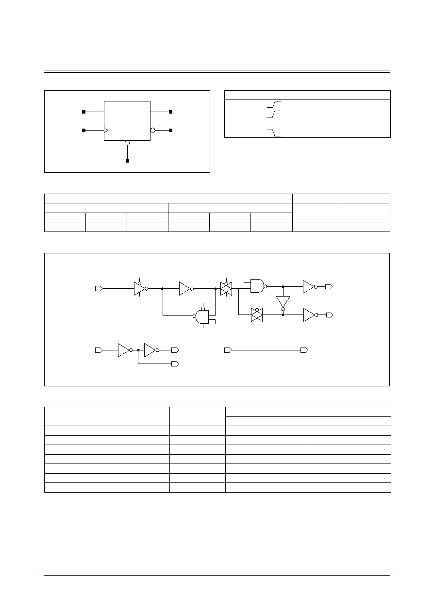
Samsung ASIC
3-229
STDL131
FD2_LP/FD2D2_LP
D Flip-Flop with Reset, 1X/2X Drive
Logic Symbol
Cell Data
Schematic Diagram
Timing Requirements
(Typical process, 25
∞
C, 1.8V, Unit = ns)
Input Load (SL)
Gate Count
FD2_LP
FD2D2_LP
FD2_LP
FD2D2_LP
D
CK
RN
D
CK
RN
0.7
1.1
1.5
0.7
1.1
1.4
6.00
7.00
Parameter
Symbol
Value (ns)
FD2_LP
FD2D2_LP
Input Setup Time (D to CK)
t
SU
0.140
0.135
Input Hold Time (D to CK)
t
HD
0.010
0.010
Pulse Width Low (CK)
t
PWL
0.215
0.214
Pulse Width High (CK)
t
PWH
0.164
0.190
Pulse Width Low (RN)
t
PWL
0.182
0.235
Recovery Time (RN to CK)
t
RC
0.010
0.010
Removal Time (RN to CK)
t
RM
0.885
0.873
D
CK
Q
QN
RN
CL
CLB
Q
CLB
CL
CLB
CL
CL
CLB
D
CK
CL
CLB
RN
QN
RN
RN
RN
Truth Table
D
CK
RN
Q (n+1) QN (n+1)
0
1
0
1
1
1
1
0
x
x
0
0
1
x
1
Q (n)
QN (n)
STDL131
3-230
Samsung ASIC
FD2_LP/FD2D2_LP
D Flip-Flop with Reset, 1X/2X Drive
Switching Characteristics
(Typical process, 25
∞
C, 1.8V, t
R
/t
F
= 0.19ns, SL: Standard Load)
FD2_LP
FD2D2_LP
Path
Parameter
Delay [ns]
SL = 2
Delay Equations [ns]
Group1*
Group2*
Group3*
CK to Q
tR
0.105
0.054 + 0.025*SL
0.052 + 0.026*SL
0.048 + 0.026*SL
tF
0.075
0.041 + 0.017*SL
0.042 + 0.017*SL
0.039 + 0.017*SL
tPLH
0.325
0.296 + 0.015*SL
0.302 + 0.013*SL
0.306 + 0.013*SL
tPHL
0.304
0.279 + 0.012*SL
0.287 + 0.011*SL
0.292 + 0.010*SL
RN to Q
tF
0.078
0.044 + 0.017*SL
0.043 + 0.017*SL
0.042 + 0.017*SL
tPHL
0.180
0.155 + 0.012*SL
0.162 + 0.011*SL
0.167 + 0.010*SL
CK to QN
tR
0.091
0.040 + 0.025*SL
0.037 + 0.026*SL
0.032 + 0.027*SL
tF
0.070
0.036 + 0.017*SL
0.035 + 0.017*SL
0.033 + 0.017*SL
tPLH
0.363
0.337 + 0.013*SL
0.339 + 0.013*SL
0.340 + 0.013*SL
tPHL
0.382
0.359 + 0.011*SL
0.365 + 0.010*SL
0.368 + 0.010*SL
RN to QN
tR
0.102
0.047 + 0.028*SL
0.049 + 0.027*SL
0.054 + 0.026*SL
tPLH
0.254
0.224 + 0.015*SL
0.228 + 0.014*SL
0.235 + 0.013*SL
*Group1 : SL < 4, *Group2 : 4 SL
<
<
=
= 8, *Group3 : 8 < SL
Path
Parameter
Delay [ns]
SL = 2
Delay Equations [ns]
Group1*
Group2*
Group3*
CK to Q
tR
0.084
0.058 + 0.013*SL
0.060 + 0.012*SL
0.055 + 0.013*SL
tF
0.063
0.045 + 0.009*SL
0.048 + 0.008*SL
0.050 + 0.008*SL
tPLH
0.341
0.322 + 0.010*SL
0.331 + 0.007*SL
0.341 + 0.006*SL
tPHL
0.318
0.301 + 0.008*SL
0.310 + 0.006*SL
0.322 + 0.005*SL
RN to Q
tF
0.063
0.046 + 0.009*SL
0.047 + 0.009*SL
0.050 + 0.008*SL
tPHL
0.192
0.175 + 0.008*SL
0.183 + 0.006*SL
0.195 + 0.005*SL
CK to QN
tR
0.067
0.044 + 0.012*SL
0.040 + 0.013*SL
0.034 + 0.013*SL
tF
0.057
0.041 + 0.008*SL
0.041 + 0.008*SL
0.036 + 0.008*SL
tPLH
0.399
0.385 + 0.007*SL
0.388 + 0.006*SL
0.391 + 0.006*SL
tPHL
0.425
0.411 + 0.007*SL
0.417 + 0.005*SL
0.424 + 0.005*SL
RN to QN
tR
0.073
0.048 + 0.013*SL
0.045 + 0.013*SL
0.049 + 0.013*SL
tPLH
0.286
0.269 + 0.008*SL
0.273 + 0.007*SL
0.280 + 0.007*SL
*Group1 : SL < 4, *Group2 : 4 SL
<
<
=
= 12, *Group3 : 12 < SL

Samsung ASIC
3-231
STDL131
FD2S_LP/FD2SD2_LP
D Flip-Flop with Reset, Scan, 1X/2X Drive
Logic Symbol
Cell Data
Schematic Diagram
Timing Requirements
(Typical process, 25
∞
C, 1.8V, Unit = ns)
Input Load (SL)
Gate Count
FD2S_LP
FD2SD2_LP
FD2S_LP
FD2SD2_LP
D
CK
RN
TI
TE
D
CK
RN
TI
TE
0.7
1.1
1.5
0.7
1.7
0.7
1.1
1.5
0.7
1.6
8.00
9.00
Parameter
Symbol
Value (ns)
FD2S_LP
FD2SD2_LP
Input Setup Time (D to CK)
t
SU
0.274
0.275
Input Hold Time (D to CK)
t
HD
0.010
0.010
Input Setup Time (TI to CK)
t
SU
0.338
0.337
Input Hold Time (TI to CK)
t
HD
0.010
0.010
Input Setup Time (TE to CK)
t
SU
0.328
0.327
Input Hold Time (TE to CK)
t
HD
0.010
0.010
Pulse Width Low (CK)
t
PWL
0.308
0.310
Pulse Width High (CK)
t
PWH
0.164
0.190
Pulse Width Low (RN)
t
PWL
0.182
0.235
Recovery Time (RN to CK)
t
RC
0.010
0.010
Removal Time (RN to CK)
t
RM
0.889
0.893
Q
QN
D
TI
TE
CK RN
CL
CLB
Q
CLB
CL
QN
CK
CL
CLB
TE
TEB
TE
RN
RN
RN
D
TE
TI
TEB
CLB
CL
RN
CL
CLB
Truth Table
D
TI
TE
CK
RN
Q
(n+1)
QN
(n+1)
0
x
0
1
0
1
1
x
0
1
1
0
x
0
1
1
0
1
x
1
1
1
1
0
x
x
x
x
0
0
1
x
x
x
1
Q(n)
QN(n)

STDL131
3-232
Samsung ASIC
FD2S_LP/FD2SD2_LP
D Flip-Flop with Reset, Scan, 1X/2X Drive
Switching Characteristics
(Typical process, 25
∞
C, 1.8V, t
R
/t
F
= 0.19ns, SL: Standard Load)
FD2S_LP
FD2SD2_LP
Path
Parameter
Delay [ns]
SL = 2
Delay Equations [ns]
Group1*
Group2*
Group3*
CK to Q
tR
0.105
0.054 + 0.025*SL
0.052 + 0.026*SL
0.047 + 0.026*SL
tF
0.074
0.040 + 0.017*SL
0.041 + 0.017*SL
0.040 + 0.017*SL
tPLH
0.328
0.298 + 0.015*SL
0.304 + 0.013*SL
0.309 + 0.013*SL
tPHL
0.309
0.284 + 0.012*SL
0.292 + 0.011*SL
0.297 + 0.010*SL
RN to Q
tF
0.077
0.044 + 0.017*SL
0.042 + 0.017*SL
0.041 + 0.017*SL
tPHL
0.180
0.155 + 0.012*SL
0.162 + 0.011*SL
0.167 + 0.010*SL
CK to QN
tR
0.091
0.040 + 0.025*SL
0.036 + 0.026*SL
0.032 + 0.027*SL
tF
0.070
0.036 + 0.017*SL
0.037 + 0.017*SL
0.031 + 0.017*SL
tPLH
0.368
0.342 + 0.013*SL
0.344 + 0.013*SL
0.345 + 0.013*SL
tPHL
0.384
0.361 + 0.011*SL
0.367 + 0.010*SL
0.370 + 0.010*SL
RN to QN
tR
0.102
0.047 + 0.028*SL
0.049 + 0.027*SL
0.054 + 0.027*SL
tPLH
0.254
0.223 + 0.015*SL
0.227 + 0.014*SL
0.235 + 0.013*SL
*Group1 : SL < 4, *Group2 : 4 SL
<
<
=
= 8, *Group3 : 8 < SL
Path
Parameter
Delay [ns]
SL = 2
Delay Equations [ns]
Group1*
Group2*
Group3*
CK to Q
tR
0.084
0.058 + 0.013*SL
0.059 + 0.012*SL
0.056 + 0.013*SL
tF
0.063
0.045 + 0.009*SL
0.048 + 0.008*SL
0.051 + 0.008*SL
tPLH
0.343
0.324 + 0.010*SL
0.333 + 0.007*SL
0.343 + 0.006*SL
tPHL
0.322
0.305 + 0.008*SL
0.314 + 0.006*SL
0.326 + 0.005*SL
RN to Q
tF
0.064
0.045 + 0.009*SL
0.049 + 0.008*SL
0.051 + 0.008*SL
tPHL
0.192
0.175 + 0.008*SL
0.184 + 0.006*SL
0.196 + 0.005*SL
CK to QN
tR
0.067
0.044 + 0.012*SL
0.040 + 0.013*SL
0.034 + 0.013*SL
tF
0.057
0.041 + 0.008*SL
0.042 + 0.008*SL
0.038 + 0.008*SL
tPLH
0.404
0.389 + 0.007*SL
0.393 + 0.006*SL
0.395 + 0.006*SL
tPHL
0.427
0.413 + 0.007*SL
0.419 + 0.005*SL
0.426 + 0.005*SL
RN to QN
tR
0.073
0.047 + 0.013*SL
0.045 + 0.013*SL
0.050 + 0.013*SL
tPLH
0.286
0.269 + 0.008*SL
0.274 + 0.007*SL
0.280 + 0.007*SL
*Group1 : SL < 4, *Group2 : 4 SL
<
<
=
= 12, *Group3 : 12 < SL
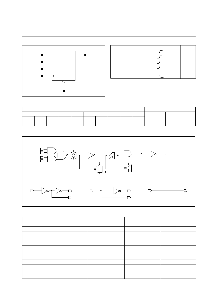
Samsung ASIC
3-233
STDL131
FD2SQ_LP/FD2SQD2_LP
D Flip-Flop with Reset, Scan, Q Output Only, 1X/2X Drive
Logic Symbol
Cell Data
Schematic Diagram
Timing Requirements
(Typical process, 25
∞
C, 1.8V, Unit = ns)
Input Load (SL)
Gate Count
FD2SQ_LP
FD2SQD2_LP
FD2SQ_LP
FD2SQD2_LP
D
CK
RN
TI
TE
D
CK
RN
TI
TE
0.7
1.1
1.4
0.7
1.6
0.7
1.1
1.4
0.7
1.6
7.33
7.67
Parameter
Symbol
Value (ns)
FD2SQ_LP
FD2SQD2_LP
Input Setup Time (D to CK)
t
SU
0.268
0.267
Input Hold Time (D to CK)
t
HD
0.010
0.010
Input Setup Time (TI to CK)
t
SU
0.332
0.330
Input Hold Time (TI to CK)
t
HD
0.010
0.010
Input Setup Time (TE to CK)
t
SU
0.327
0.326
Input Hold Time (TE to CK)
t
HD
0.010
0.010
Pulse Width Low (CK)
t
PWL
0.308
0.307
Pulse Width High (CK)
t
PWH
0.145
0.152
Pulse Width Low (RN)
t
PWL
0.206
0.226
Recovery Time (RN to CK)
t
RC
0.010
0.010
Removal Time (RN to CK)
t
RM
0.890
0.888
Q
D
TI
TE
CK RN
CL
CLB
Q
CLB
CL
CLB
CL
CL
CLB
CK
CL
CLB
TE
TEB
TE
RN
RN
RN
D
TE
TI
TEB
RN
Truth Table
D
TI
TE
CK
RN
Q (n+1)
0
x
0
1
0
1
x
0
1
1
x
0
1
1
0
x
1
1
1
1
x
x
x
x
0
0
x
x
x
1
Q(n)
STDL131
3-234
Samsung ASIC
FD2SQ_LP/FD2SQD2_LP
D Flip-Flop with Reset, Scan, Q Output Only, 1X/2X Drive
Switching Characteristics
(Typical process, 25
∞
C, 1.8V, t
R
/t
F
= 0.19ns, SL: Standard Load)
FD2SQ_LP
FD2SQD2_LP
Path
Parameter
Delay [ns]
SL = 2
Delay Equations [ns]
Group1*
Group2*
Group3*
CK to Q
tR
0.100
0.051 + 0.025*SL
0.046 + 0.026*SL
0.041 + 0.027*SL
tF
0.070
0.036 + 0.017*SL
0.037 + 0.017*SL
0.033 + 0.017*SL
tPLH
0.315
0.287 + 0.014*SL
0.292 + 0.013*SL
0.294 + 0.013*SL
tPHL
0.299
0.276 + 0.012*SL
0.281 + 0.010*SL
0.284 + 0.010*SL
RN to Q
tF
0.071
0.036 + 0.017*SL
0.038 + 0.017*SL
0.033 + 0.017*SL
tPHL
0.166
0.143 + 0.012*SL
0.149 + 0.010*SL
0.152 + 0.010*SL
*Group1 : SL < 4, *Group2 : 4 SL
<
<
=
= 8, *Group3 : 8 < SL
Path
Parameter
Delay [ns]
SL = 2
Delay Equations [ns]
Group1*
Group2*
Group3*
CK to Q
tR
0.076
0.052 + 0.012*SL
0.050 + 0.013*SL
0.045 + 0.013*SL
tF
0.054
0.036 + 0.009*SL
0.038 + 0.008*SL
0.037 + 0.008*SL
tPLH
0.320
0.302 + 0.009*SL
0.310 + 0.007*SL
0.317 + 0.006*SL
tPHL
0.304
0.289 + 0.007*SL
0.296 + 0.006*SL
0.305 + 0.005*SL
RN to Q
tF
0.057
0.037 + 0.010*SL
0.043 + 0.008*SL
0.039 + 0.009*SL
tPHL
0.170
0.155 + 0.007*SL
0.162 + 0.006*SL
0.170 + 0.005*SL
*Group1 : SL < 4, *Group2 : 4 SL
<
<
=
= 12, *Group3 : 12 < SL
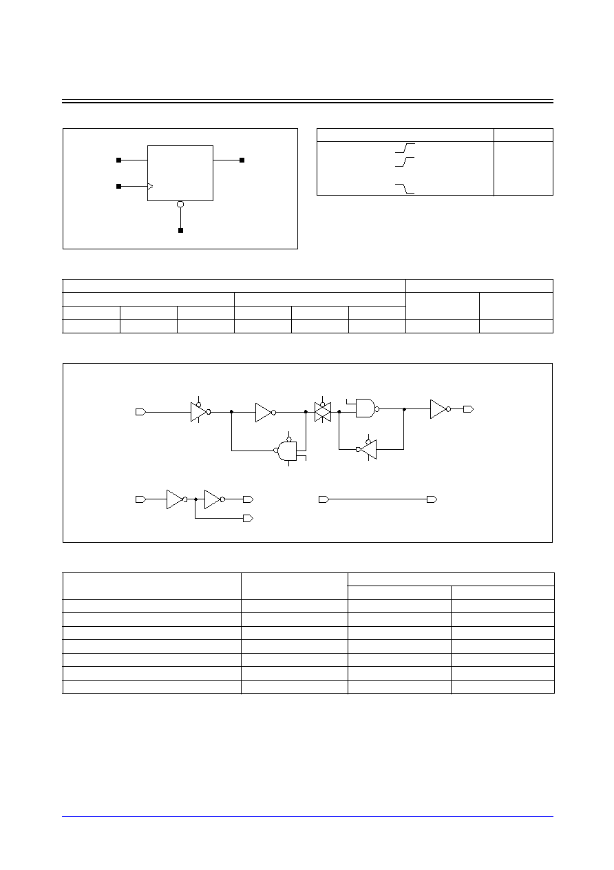
Samsung ASIC
3-235
STDL131
FD2Q_LP/FD2QD2_LP
D Flip-Flop with Reset, Q Output Only, 1X/2X Drive
Logic Symbol
Cell Data
Schematic Diagram
Timing Requirements
(Typical process, 25
∞
C, 1.8V, Unit = ns)
Input Load (SL)
Gate Count
FD2Q_LP
FD2QD2_LP
FD2Q_LP
FD2QD2_LP
D
CK
RN
D
CK
RN
0.7
1.1
1.5
0.7
1.1
1.4
5.33
5.33
Parameter
Symbol
Value (ns)
FD2Q_LP
FD2QD2_LP
Input Setup Time (D to CK)
t
SU
0.133
0.135
Input Hold Time (D to CK)
t
HD
0.010
0.010
Pulse Width Low (CK)
t
PWL
0.212
0.213
Pulse Width High (CK)
t
PWH
0.145
0.153
Pulse Width Low (RN)
t
PWL
0.208
0.226
Recovery Time (RN to CK)
t
RC
0.010
0.010
Removal Time (RN to CK)
t
RM
0.865
0.873
D
CK
Q
RN
CL
CLB
Q
CLB
CL
CL
CLB
D
CK
CL
CLB
RN
RN
RN
RN
CLB
CL
Truth Table
D
CK
RN
Q (n+1)
0
1
0
1
1
1
x
x
0
0
x
x
Q (n)

STDL131
3-236
Samsung ASIC
FD2Q_LP/FD2QD2_LP
D Flip-Flop with Reset, Q Output Only, 1X/2X Drive
Switching Characteristics
(Typical process, 25
∞
C, 1.8V, t
R
/t
F
= 0.19ns, SL: Standard Load)
FD2Q_LP
FD2QD2_LP
Path
Parameter
Delay [ns]
SL = 2
Delay Equations [ns]
Group1*
Group2*
Group3*
CK to Q
tR
0.100
0.051 + 0.025*SL
0.047 + 0.026*SL
0.042 + 0.026*SL
tF
0.071
0.037 + 0.017*SL
0.038 + 0.017*SL
0.032 + 0.017*SL
tPLH
0.315
0.287 + 0.014*SL
0.292 + 0.013*SL
0.294 + 0.013*SL
tPHL
0.291
0.268 + 0.012*SL
0.274 + 0.010*SL
0.277 + 0.010*SL
RN to Q
tF
0.072
0.038 + 0.017*SL
0.039 + 0.017*SL
0.034 + 0.017*SL
tPHL
0.168
0.145 + 0.012*SL
0.151 + 0.010*SL
0.154 + 0.010*SL
*Group1 : SL < 4, *Group2 : 4 SL
<
<
=
= 8, *Group3 : 8 < SL
Path
Parameter
Delay [ns]
SL = 2
Delay Equations [ns]
Group1*
Group2*
Group3*
CK to Q
tR
0.077
0.053 + 0.012*SL
0.052 + 0.012*SL
0.047 + 0.013*SL
tF
0.056
0.038 + 0.009*SL
0.041 + 0.008*SL
0.039 + 0.008*SL
tPLH
0.321
0.303 + 0.009*SL
0.310 + 0.007*SL
0.318 + 0.006*SL
tPHL
0.295
0.281 + 0.007*SL
0.287 + 0.006*SL
0.296 + 0.005*SL
RN to Q
tF
0.058
0.039 + 0.010*SL
0.045 + 0.008*SL
0.040 + 0.009*SL
tPHL
0.172
0.157 + 0.007*SL
0.163 + 0.006*SL
0.172 + 0.005*SL
*Group1 : SL < 4, *Group2 : 4 SL
<
<
=
= 12, *Group3 : 12 < SL
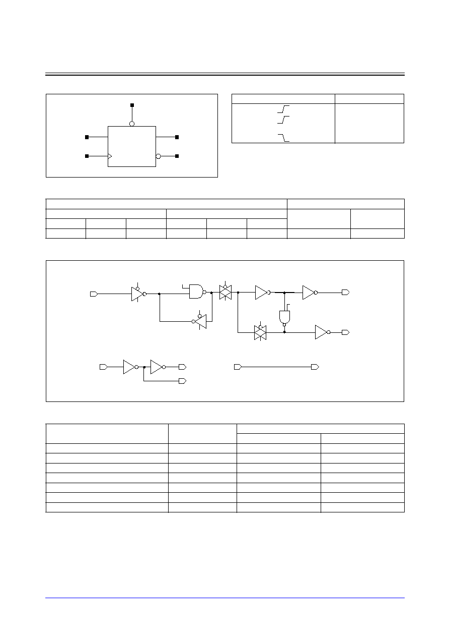
Samsung ASIC
3-237
STDL131
FD3_LP/FD3D2_LP
D Flip-Flop with Set, 1X/2X Drive
Logic Symbol
Cell Data
Schematic Diagram
Timing Requirements
(Typical process, 25
∞
C, 1.8V, Unit = ns)
Input Load (SL)
Gate Count
FD3_LP
FD3D2_LP
FD3_LP
FD3D2_LP
D
CK
SN
D
CK
SN
0.7
1.1
2.0
0.7
1.1
2.1
6.33
7.00
Parameter
Symbol
Value (ns)
FD3_LP
FD3D2_LP
Input Setup Time (D to CK)
t
SU
0.136
0.137
Input Hold Time (D to CK)
t
HD
0.010
0.010
Pulse Width Low (CK)
t
PWL
0.233
0.235
Pulse Width High (CK)
t
PWH
0.162
0.176
Pulse Width Low (SN)
t
PWL
0.336
0.370
Recovery Time (SN to CK)
t
RC
0.010
0.010
Removal Time (SN to CK)
t
RM
0.172
0.172
D
CK
Q
QN
SN
Q
CLB
CL
CLB
CL
QN
D
CK
CL
CLB
CL
CLB
SN
SN
SN
CLB
CL
SN
Truth Table
D
CK
SN
Q (n+1) QN (n+1)
0
1
0
1
1
1
1
0
x
x
0
1
0
x
1
Q (n)
QN (n)

STDL131
3-238
Samsung ASIC
FD3_LP/FD3D2_LP
D Flip-Flop with Set, 1X/2X Drive
Switching Characteristics
(Typical process, 25
∞
C, 1.8V, t
R
/t
F
= 0.19ns, SL: Standard Load)
FD3_LP
FD3D2_LP
Path
Parameter
Delay [ns]
SL = 2
Delay Equations [ns]
Group1*
Group2*
Group3*
CK to Q
tR
0.096
0.045 + 0.025*SL
0.041 + 0.026*SL
0.038 + 0.027*SL
tF
0.072
0.038 + 0.017*SL
0.040 + 0.016*SL
0.038 + 0.017*SL
tPLH
0.303
0.276 + 0.014*SL
0.279 + 0.013*SL
0.280 + 0.013*SL
tPHL
0.311
0.288 + 0.012*SL
0.294 + 0.010*SL
0.298 + 0.010*SL
SN to Q
tR
0.111
0.066 + 0.023*SL
0.057 + 0.025*SL
0.048 + 0.026*SL
tPLH
0.470
0.441 + 0.014*SL
0.448 + 0.013*SL
0.449 + 0.013*SL
CK to QN
tR
0.101
0.052 + 0.025*SL
0.047 + 0.026*SL
0.043 + 0.026*SL
tF
0.071
0.038 + 0.017*SL
0.039 + 0.016*SL
0.037 + 0.017*SL
tPLH
0.409
0.380 + 0.014*SL
0.386 + 0.013*SL
0.389 + 0.013*SL
tPHL
0.371
0.347 + 0.012*SL
0.354 + 0.010*SL
0.358 + 0.010*SL
SN to QN
tF
0.080
0.045 + 0.018*SL
0.047 + 0.017*SL
0.044 + 0.018*SL
tPHL
0.194
0.168 + 0.013*SL
0.176 + 0.011*SL
0.182 + 0.010*SL
*Group1 : SL < 4, *Group2 : 4 SL
<
<
=
= 8, *Group3 : 8 < SL
Path
Parameter
Delay [ns]
SL = 2
Delay Equations [ns]
Group1*
Group2*
Group3*
CK to Q
tR
0.069
0.044 + 0.012*SL
0.043 + 0.013*SL
0.037 + 0.013*SL
tF
0.059
0.040 + 0.009*SL
0.045 + 0.008*SL
0.042 + 0.008*SL
tPLH
0.304
0.288 + 0.008*SL
0.294 + 0.007*SL
0.298 + 0.006*SL
tPHL
0.319
0.304 + 0.008*SL
0.311 + 0.006*SL
0.321 + 0.005*SL
SN to Q
tR
0.086
0.061 + 0.013*SL
0.064 + 0.012*SL
0.050 + 0.013*SL
tPLH
0.496
0.477 + 0.010*SL
0.487 + 0.007*SL
0.495 + 0.006*SL
CK to QN
tR
0.075
0.051 + 0.012*SL
0.050 + 0.012*SL
0.044 + 0.013*SL
tF
0.057
0.041 + 0.008*SL
0.041 + 0.008*SL
0.039 + 0.008*SL
tPLH
0.433
0.415 + 0.009*SL
0.423 + 0.007*SL
0.430 + 0.006*SL
tPHL
0.395
0.380 + 0.008*SL
0.387 + 0.006*SL
0.397 + 0.005*SL
SN to QN
tF
0.063
0.043 + 0.010*SL
0.047 + 0.009*SL
0.046 + 0.009*SL
tPHL
0.190
0.173 + 0.008*SL
0.181 + 0.006*SL
0.192 + 0.005*SL
*Group1 : SL < 4, *Group2 : 4 SL
<
<
=
= 12, *Group3 : 12 < SL
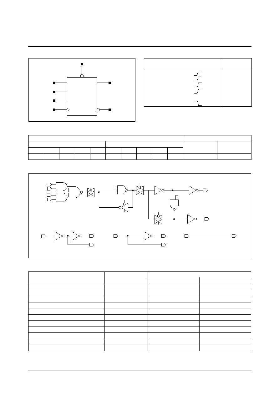
Samsung ASIC
3-239
STDL131
FD3S_LP/FD3SD2_LP
D Flip-Flop with Set, Scan, 1X/2X Drive
Logic Symbol
Cell Data
Schematic Diagram
Timing Requirements
(Typical process, 25
∞
C, 1.8V, Unit = ns)
Input Load (SL)
Gate Count
FD3S_LP
FD3SD2_LP
FD3S_LP
FD3SD2_LP
D
CK
SN
TI
TE
D
CK
SN
TI
TE
0.7
1.1
2.0
0.7
1.6
0.7
1.1
2.2
0.7
1.6
8.00
8.67
Parameter
Symbol
Value (ns)
FD3S_LP
FD3SD2_LP
Input Setup Time (D to CK)
t
SU
0.305
0.306
Input Hold Time (D to CK)
t
HD
0.010
0.010
Pulse Width Low (CK)
t
PWL
0.338
0.340
Pulse Width High (CK)
t
PWH
0.162
0.179
Pulse Width Low (SN)
t
PWL
0.331
0.374
Recovery Time (SN to CK)
t
RC
0.010
0.010
Removal Time (SN to CK)
t
RM
0.165
0.166
Input Setup Time (TI to CK)
t
SU
0.361
0.361
Input Hold Time (TI to CK)
t
HD
0.010
0.010
Input Setup Time (TE to CK)
t
SU
0.342
0.343
Input Hold Time (TE to CK)
t
HD
0.010
0.010
Q
QN
D
TI
TE
CK
SN
CL
CLB
QN
CLB
CL
CLB
CL
Q
CK
CL
CLB
TE
TEB
TE
SN
SN
SN
D
TE
TI
TEB
CL
CLB
SN
Truth Table
D
TI
TE
CK
SN
Q
(n+1)
QN
(n+1)
0
x
0
1
0
1
1
x
0
1
1
0
x
0
1
1
0
1
x
1
1
1
1
0
x
x
x
x
0
1
0
x
x
x
1
Q (n) QN (n)

STDL131
3-240
Samsung ASIC
FD3S_LP/FD3SD2_LP
D Flip-Flop with Set, Scan, 1X/2X Drive
Switching Characteristics
(Typical process, 25
∞
C, 1.8V, t
R
/t
F
= 0.19ns, SL: Standard Load)
FD3S_LP
FD3SD2_LP
Path
Parameter
Delay [ns]
SL = 2
Delay Equations [ns]
Group1*
Group2*
Group3*
CK to Q
tR
0.095
0.044 + 0.026*SL
0.041 + 0.026*SL
0.037 + 0.027*SL
tF
0.073
0.039 + 0.017*SL
0.040 + 0.017*SL
0.037 + 0.017*SL
tPLH
0.302
0.275 + 0.014*SL
0.278 + 0.013*SL
0.279 + 0.013*SL
tPHL
0.310
0.286 + 0.012*SL
0.293 + 0.010*SL
0.297 + 0.010*SL
SN to Q
tR
0.109
0.062 + 0.023*SL
0.054 + 0.025*SL
0.046 + 0.026*SL
tPLH
0.463
0.434 + 0.015*SL
0.441 + 0.013*SL
0.443 + 0.013*SL
CK to QN
tR
0.102
0.053 + 0.025*SL
0.050 + 0.025*SL
0.044 + 0.026*SL
tF
0.074
0.040 + 0.017*SL
0.040 + 0.017*SL
0.036 + 0.017*SL
tPLH
0.406
0.377 + 0.014*SL
0.383 + 0.013*SL
0.385 + 0.013*SL
tPHL
0.370
0.346 + 0.012*SL
0.353 + 0.010*SL
0.356 + 0.010*SL
SN to QN
tF
0.082
0.047 + 0.017*SL
0.045 + 0.018*SL
0.043 + 0.018*SL
tPHL
0.193
0.167 + 0.013*SL
0.174 + 0.011*SL
0.179 + 0.010*SL
*Group1 : SL < 4, *Group2 : 4 SL
<
<
=
= 8, *Group3 : 8 < SL
Path
Parameter
Delay [ns]
SL = 2
Delay Equations [ns]
Group1*
Group2*
Group3*
CK to Q
tR
0.069
0.044 + 0.012*SL
0.043 + 0.013*SL
0.037 + 0.013*SL
tF
0.059
0.040 + 0.009*SL
0.044 + 0.008*SL
0.042 + 0.008*SL
tPLH
0.306
0.289 + 0.008*SL
0.295 + 0.007*SL
0.299 + 0.006*SL
tPHL
0.319
0.304 + 0.008*SL
0.311 + 0.006*SL
0.321 + 0.005*SL
SN to Q
tR
0.086
0.060 + 0.013*SL
0.064 + 0.012*SL
0.050 + 0.013*SL
tPLH
0.498
0.479 + 0.010*SL
0.490 + 0.007*SL
0.497 + 0.006*SL
CK to QN
tR
0.076
0.052 + 0.012*SL
0.051 + 0.012*SL
0.043 + 0.013*SL
tF
0.057
0.038 + 0.009*SL
0.044 + 0.008*SL
0.041 + 0.008*SL
tPLH
0.432
0.415 + 0.009*SL
0.422 + 0.007*SL
0.429 + 0.006*SL
tPHL
0.398
0.382 + 0.008*SL
0.390 + 0.006*SL
0.400 + 0.005*SL
SN to QN
tF
0.063
0.043 + 0.010*SL
0.048 + 0.009*SL
0.046 + 0.009*SL
tPHL
0.191
0.175 + 0.008*SL
0.183 + 0.006*SL
0.194 + 0.005*SL
*Group1 : SL < 4, *Group2 : 4 SL
<
<
=
= 12, *Group3 : 12 < SL
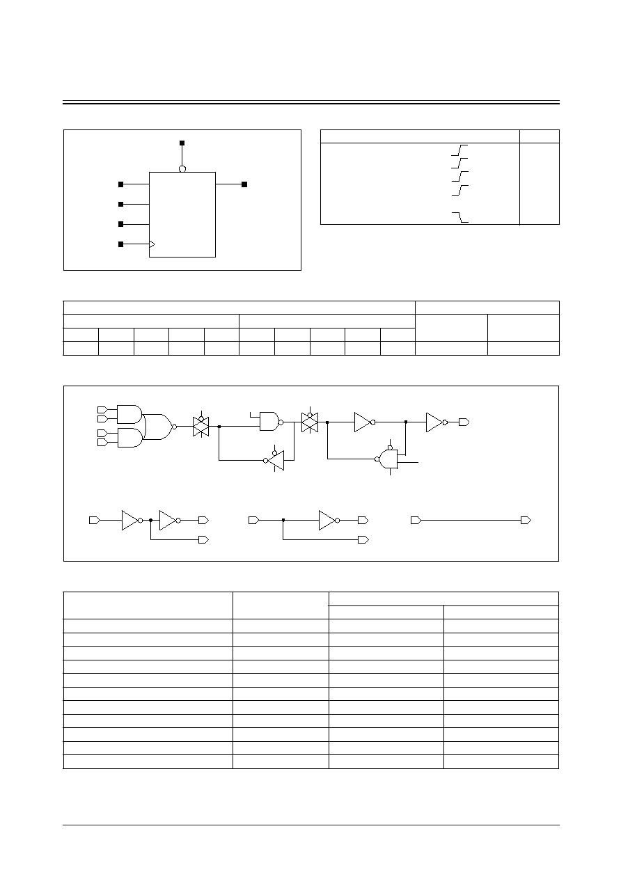
Samsung ASIC
3-241
STDL131
FD3SQ_LP/FD3SQD2_LP
D Flip-Flop with Set, Scan, Q Output Only, 1X/2X Drive
Logic Symbol
Cell Data
Schematic Diagram
Timing Requirements
(Typical process, 25
∞
C, 1.8V, Unit = ns)
Input Load (SL)
Gate Count
FD3SQ_LP
FD3SQD2_LP
FD3SQ_LP
FD3SQD2_LP
D
CK
SN
TI
TE
D
CK
SN
TI
TE
0.7
1.1
1.3
0.7
1.6
0.7
1.1
1.3
0.7
1.6
7.33
7.67
Parameter
Symbol
Value (ns)
FD3SQ_LP
FD3SQD2_LP
Input Setup Time (D to CK)
t
SU
0.305
0.304
Input Hold Time (D to CK)
t
HD
0.010
0.010
Pulse Width Low (CK)
t
PWL
0.337
0.336
Pulse Width High (CK)
t
PWH
0.139
0.145
Pulse Width Low (SN)
t
PWL
0.988
1.017
Recovery Time (SN to CK)
t
RC
0.010
0.010
Removal Time (SN to CK)
t
RM
0.166
0.165
Input Setup Time (TI to CK)
t
SU
0.360
0.359
Input Hold Time (TI to CK)
t
HD
0.010
0.010
Input Setup Time (TE to CK)
t
SU
0.340
0.340
Input Hold Time (TE to CK)
t
HD
0.010
0.010
Q
D
TI
TE
CK
SN
CL
CLB
CLB
CL
CL
CLB
CK
CL
CLB
TE
TEB
TE
SN
SN
SN
Q
D
TE
TI
TEB
CLB
CL
SN
Truth Table
D
TI
TE
CK
SN
Q (n+1)
0
x
0
1
0
1
x
0
1
1
x
0
1
1
0
x
1
1
1
1
x
x
x
x
0
1
x
x
x
1
Q (n)
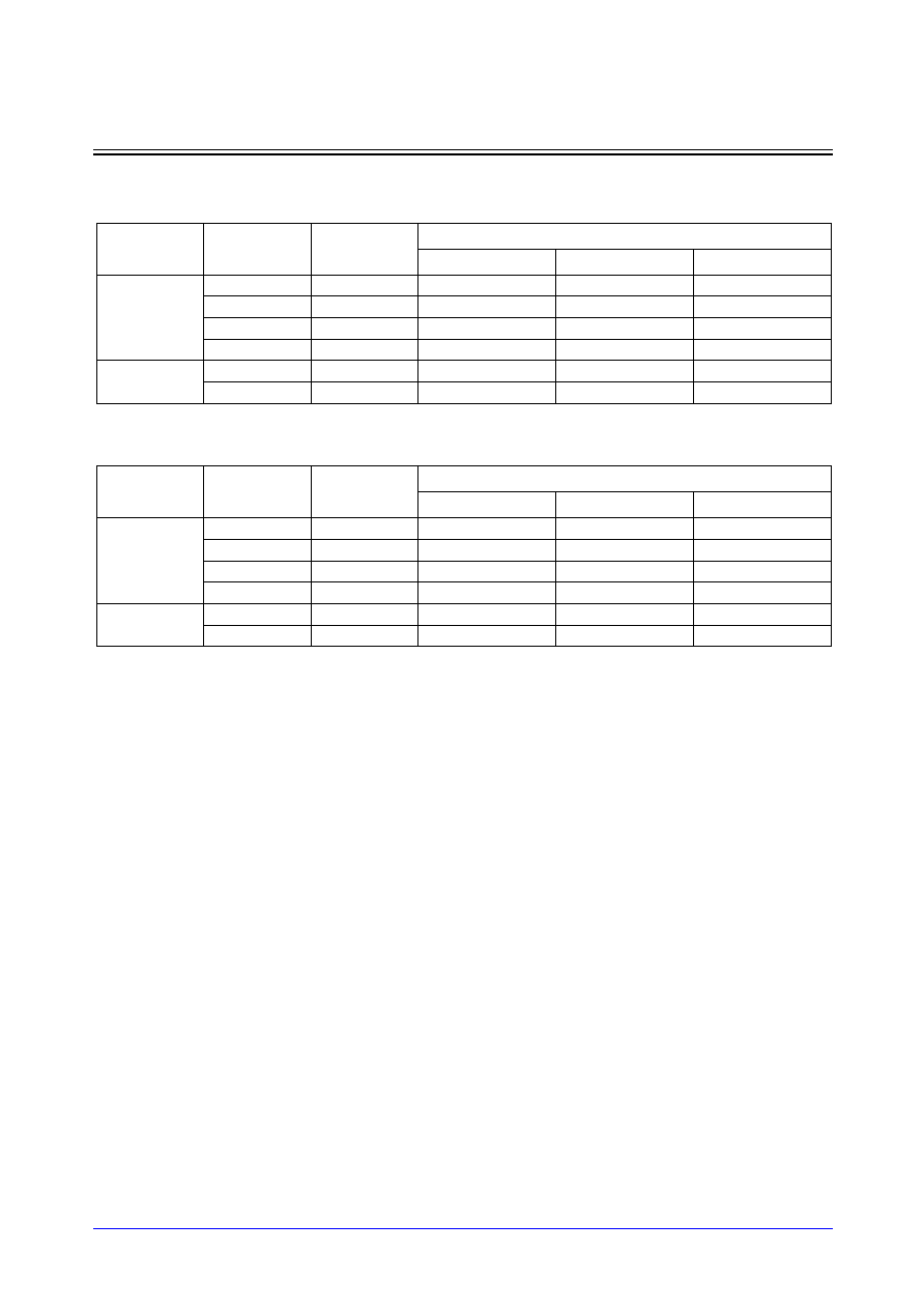
STDL131
3-242
Samsung ASIC
FD3SQ_LP/FD3SQD2_LP
D Flip-Flop with Set, Scan, Q Output Only, 1X/2X Drive
Switching Characteristics
(Typical process, 25
∞
C, 1.8V, t
R
/t
F
= 0.19ns, SL: Standard Load)
FD3SQ_LP
FD3SQD2_LP
Path
Parameter
Delay [ns]
SL = 2
Delay Equations [ns]
Group1*
Group2*
Group3*
CK to Q
tR
0.090
0.039 + 0.026*SL
0.037 + 0.026*SL
0.033 + 0.027*SL
tF
0.067
0.033 + 0.017*SL
0.033 + 0.017*SL
0.031 + 0.017*SL
tPLH
0.288
0.261 + 0.013*SL
0.263 + 0.013*SL
0.264 + 0.013*SL
tPHL
0.294
0.271 + 0.011*SL
0.277 + 0.010*SL
0.279 + 0.010*SL
SN to Q
tR
0.117
0.072 + 0.022*SL
0.063 + 0.024*SL
0.053 + 0.026*SL
tPLH
0.912
0.880 + 0.016*SL
0.892 + 0.013*SL
0.896 + 0.013*SL
*Group1 : SL < 4, *Group2 : 4 SL
<
<
=
= 8, *Group3 : 8 < SL
Path
Parameter
Delay [ns]
SL = 2
Delay Equations [ns]
Group1*
Group2*
Group3*
CK to Q
tR
0.065
0.041 + 0.012*SL
0.039 + 0.013*SL
0.032 + 0.013*SL
tF
0.054
0.036 + 0.009*SL
0.038 + 0.008*SL
0.035 + 0.009*SL
tPLH
0.291
0.275 + 0.008*SL
0.280 + 0.007*SL
0.283 + 0.006*SL
tPHL
0.302
0.287 + 0.007*SL
0.294 + 0.006*SL
0.301 + 0.005*SL
SN to Q
tR
0.096
0.071 + 0.012*SL
0.076 + 0.011*SL
0.060 + 0.013*SL
tPLH
0.928
0.906 + 0.011*SL
0.922 + 0.007*SL
0.933 + 0.006*SL
*Group1 : SL < 4, *Group2 : 4 SL
<
<
=
= 12, *Group3 : 12 < SL
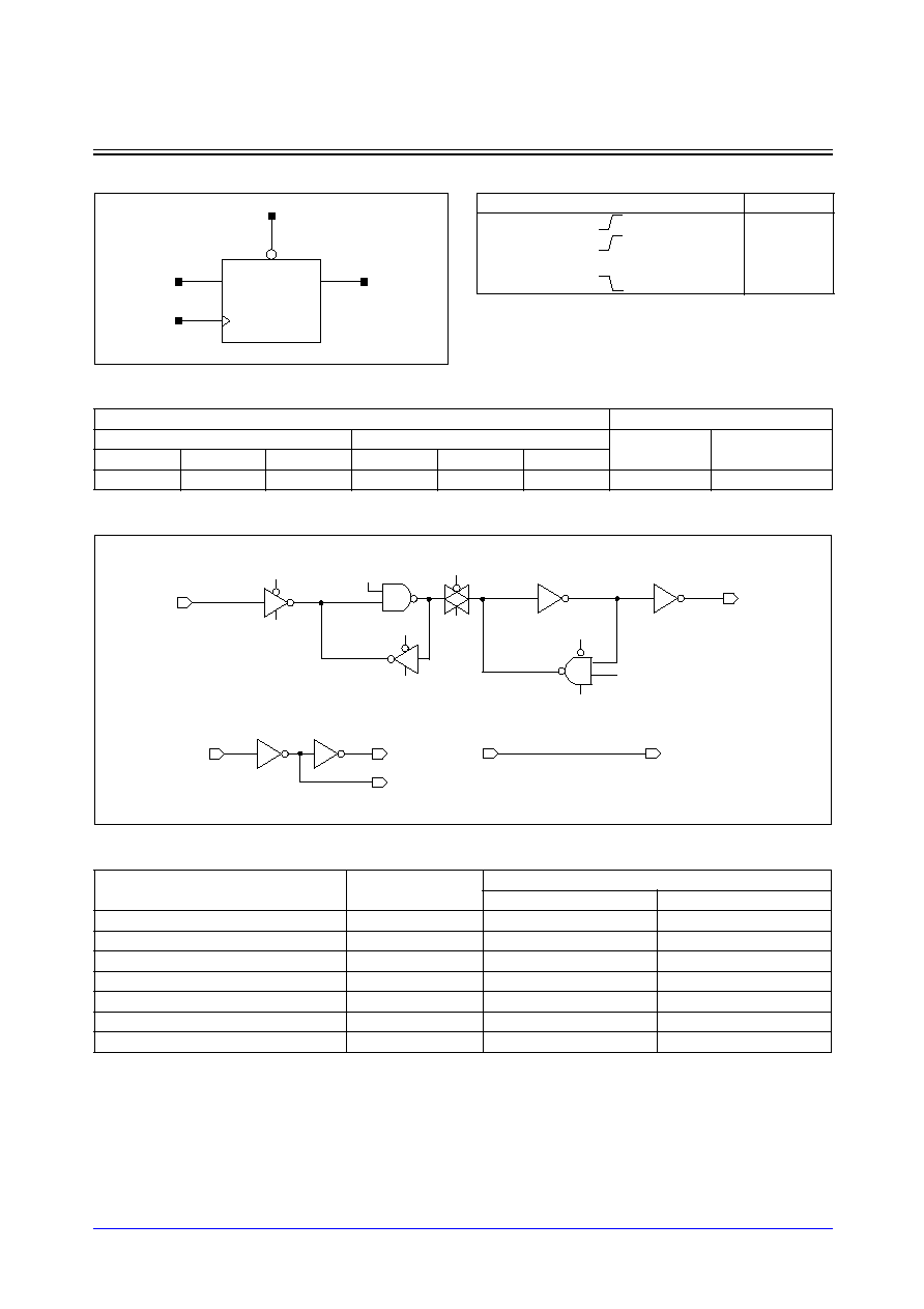
Samsung ASIC
3-243
STDL131
FD3Q_LP/FD3QD2_LP
D Flip-Flop with Set, Q Output Only, 1X/2X Drive
Logic Symbol
Cell Data
Schematic Diagram
Timing Requirements
(Typical process, 25
∞
C, 1.8V, Unit = ns)
Input Load (SL)
Gate Count
FD3Q_LP
FD3QD2_LP
FD3Q_LP
FD3QD2_LP
D
CK
SN
D
CK
SN
0.7
1.1
1.3
0.7
1.1
1.3
5.67
6.00
Parameter
Symbol
Value (ns)
FD3Q_LP
FD3QD2_LP
Input Setup Time (D to CK)
t
SU
0.136
0.136
Input Hold Time (D to CK)
t
HD
0.010
0.010
Pulse Width Low (CK)
t
PWL
0.231
0.232
Pulse Width High (CK)
t
PWH
0.139
0.145
Pulse Width Low (SN)
t
PWL
1.000
1.034
Recovery Time (SN to CK)
t
RC
0.010
0.010
Removal Time (SN to CK)
t
RM
0.172
0.173
D
CK
Q
SN
Q
CLB
CL
CLB
CL
CL
CLB
D
CK
CL
CLB
CL
CLB
SN
SN
SN
SN
Truth Table
D
CK
SN
Q (n+1)
0
1
0
1
1
1
x
x
0
1
x
x
Q (n)

STDL131
3-244
Samsung ASIC
FD3Q_LP/FD3QD2_LP
D Flip-Flop with Set, Q Output Only, 1X/2X Drive
Switching Characteristics
(Typical process, 25
∞
C, 1.8V, t
R
/t
F
= 0.19ns, SL: Standard Load)
FD3Q_LP
FD3QD2_LP
Path
Parameter
Delay [ns]
SL = 2
Delay Equations [ns]
Group1*
Group2*
Group3*
CK to Q
tR
0.092
0.042 + 0.025*SL
0.037 + 0.026*SL
0.033 + 0.027*SL
tF
0.068
0.034 + 0.017*SL
0.035 + 0.017*SL
0.029 + 0.017*SL
tPLH
0.288
0.261 + 0.013*SL
0.263 + 0.013*SL
0.264 + 0.013*SL
tPHL
0.296
0.274 + 0.011*SL
0.279 + 0.010*SL
0.282 + 0.010*SL
SN to Q
tR
0.117
0.072 + 0.023*SL
0.064 + 0.024*SL
0.054 + 0.026*SL
tPLH
0.922
0.889 + 0.016*SL
0.902 + 0.013*SL
0.905 + 0.013*SL
*Group1 : SL < 4, *Group2 : 4 SL
<
<
=
= 8, *Group3 : 8 < SL
Path
Parameter
Delay [ns]
SL = 2
Delay Equations [ns]
Group1*
Group2*
Group3*
CK to Q
tR
0.067
0.044 + 0.011*SL
0.039 + 0.013*SL
0.033 + 0.013*SL
tF
0.053
0.036 + 0.008*SL
0.036 + 0.008*SL
0.036 + 0.008*SL
tPLH
0.291
0.275 + 0.008*SL
0.280 + 0.007*SL
0.283 + 0.006*SL
tPHL
0.304
0.289 + 0.007*SL
0.296 + 0.006*SL
0.303 + 0.005*SL
SN to Q
tR
0.096
0.072 + 0.012*SL
0.074 + 0.011*SL
0.061 + 0.013*SL
tPLH
0.942
0.920 + 0.011*SL
0.936 + 0.007*SL
0.947 + 0.006*SL
*Group1 : SL < 4, *Group2 : 4 SL
<
<
=
= 12, *Group3 : 12 < SL
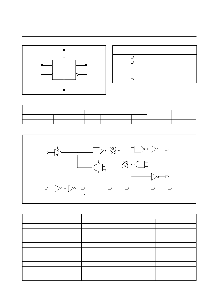
Samsung ASIC
3-245
STDL131
FD4_LP/FD4D2_LP
D Flip-Flop with Reset, Set, 1X/2X Drive
Logic Symbol
Cell Data
Schematic Diagram
Timing Requirements
(Typical process, 25
∞
C, 1.8V, Unit = ns)
Input Load (SL)
Gate Count
FD4_LP
FD4D2_LP
FD4_LP
FD4D2_LP
D
CK
RN
SN
D
CK
RN
SN
0.7
1.1
1.7
2.0
0.7
1.1
1.8
2.2
7.67
8.00
Parameter
Symbol
Value (ns)
FD4_LP
FD4D2_LP
Input Setup Time (D to CK)
t
SU
0.137
0.137
Input Hold Time (D to CK)
t
HD
0.010
0.010
Pulse Width Low (CK)
t
PWL
0.233
0.232
Pulse Width High (CK)
t
PWH
0.182
0.204
Pulse Width Low (RN)
t
PWL
0.246
0.280
Pulse Width Low (SN)
t
PWL
0.369
0.411
Recovery Time (RN to CK)
t
RC
0.010
0.010
Removal Time (RN to CK)
t
RM
0.919
0.917
Recovery Time (SN to CK)
t
RC
0.010
0.010
Removal Time (SN to CK)
t
RM
0.213
0.212
Removal Time (SN to RN)
t
RM
0.060
0.057
Recovery Time (SN to RN)
t
RC
0.010
0.010
D
CK
Q
QN
RN
SN
D
CK
CL
CLB
Q
CL
CLB
CL
CLB
CL
CL
CLB
QN
CLB
SN
SN
RN
RN
RN
RN
SN
SN
Truth Table
D
CK
RN
SN
Q
(n+1)
QN
(n+1)
0
1
1
0
1
1
1
1
1
0
x
x
1
0
1
0
x
x
0
1
0
1
x
x
0
0
0
0
x
1
1
Q (n)
QN (n)

STDL131
3-246
Samsung ASIC
FD4_LP/FD4D2_LP
D Flip-Flop with Reset, Set, 1X/2X Drive
Switching Characteristics
(Typical process, 25
∞
C, 1.8V, t
R
/t
F
= 0.19ns, SL: Standard Load)
FD4_LP
Path
Parameter
Delay [ns]
SL = 2
Delay Equations [ns]
Group1*
Group2*
Group3*
CK to Q
tR
0.107
0.057 + 0.025*SL
0.055 + 0.025*SL
0.050 + 0.026*SL
tF
0.077
0.043 + 0.017*SL
0.045 + 0.016*SL
0.041 + 0.017*SL
tPLH
0.342
0.312 + 0.015*SL
0.319 + 0.013*SL
0.322 + 0.013*SL
tPHL
0.334
0.309 + 0.012*SL
0.317 + 0.010*SL
0.322 + 0.010*SL
RN to Q
tR
0.104
0.055 + 0.025*SL
0.052 + 0.025*SL
0.047 + 0.026*SL
tF
0.077
0.045 + 0.016*SL
0.043 + 0.017*SL
0.039 + 0.017*SL
tPLH
0.171
0.142 + 0.014*SL
0.149 + 0.013*SL
0.152 + 0.012*SL
tPHL
0.182
0.158 + 0.012*SL
0.165 + 0.010*SL
0.170 + 0.010*SL
SN to Q
tR
0.119
0.073 + 0.023*SL
0.068 + 0.024*SL
0.060 + 0.025*SL
tPLH
0.518
0.487 + 0.016*SL
0.497 + 0.013*SL
0.501 + 0.013*SL
CK to QN
tR
0.104
0.055 + 0.024*SL
0.051 + 0.025*SL
0.046 + 0.026*SL
tF
0.075
0.042 + 0.017*SL
0.042 + 0.016*SL
0.040 + 0.017*SL
tPLH
0.439
0.410 + 0.014*SL
0.416 + 0.013*SL
0.419 + 0.012*SL
tPHL
0.418
0.394 + 0.012*SL
0.401 + 0.010*SL
0.406 + 0.010*SL
RN to QN
tR
0.123
0.065 + 0.029*SL
0.072 + 0.027*SL
0.081 + 0.026*SL
tPLH
0.311
0.276 + 0.018*SL
0.284 + 0.016*SL
0.295 + 0.014*SL
SN to QN
tR
0.120
0.062 + 0.029*SL
0.071 + 0.027*SL
0.080 + 0.026*SL
tF
0.083
0.048 + 0.018*SL
0.050 + 0.017*SL
0.047 + 0.018*SL
tPLH
0.190
0.155 + 0.017*SL
0.162 + 0.016*SL
0.175 + 0.014*SL
tPHL
0.202
0.175 + 0.013*SL
0.183 + 0.011*SL
0.189 + 0.010*SL
*Group1 : SL < 4, *Group2 : 4 SL
<
<
=
= 8, *Group3 : 8 < SL
Samsung ASIC
3-247
STDL131
FD4_LP/FD4D2_LP
D Flip-Flop with Reset, Set, 1X/2X Drive
Switching Characteristics
(Typical process, 25
∞
C, 1.8V, t
R
/t
F
= 0.19ns, SL: Standard Load)
FD4D2_LP
Path
Parameter
Delay [ns]
SL = 2
Delay Equations [ns]
Group1*
Group2*
Group3*
CK to Q
tR
0.084
0.059 + 0.013*SL
0.060 + 0.012*SL
0.054 + 0.013*SL
tF
0.064
0.046 + 0.009*SL
0.050 + 0.008*SL
0.048 + 0.008*SL
tPLH
0.348
0.329 + 0.009*SL
0.338 + 0.007*SL
0.348 + 0.006*SL
tPHL
0.341
0.325 + 0.008*SL
0.333 + 0.006*SL
0.344 + 0.005*SL
RN to Q
tR
0.083
0.059 + 0.012*SL
0.057 + 0.012*SL
0.053 + 0.013*SL
tF
0.063
0.044 + 0.009*SL
0.050 + 0.008*SL
0.046 + 0.008*SL
tPLH
0.176
0.158 + 0.009*SL
0.166 + 0.007*SL
0.176 + 0.006*SL
tPHL
0.188
0.172 + 0.008*SL
0.180 + 0.006*SL
0.191 + 0.005*SL
SN to Q
tR
0.097
0.072 + 0.013*SL
0.076 + 0.012*SL
0.066 + 0.013*SL
tPLH
0.553
0.532 + 0.010*SL
0.543 + 0.007*SL
0.556 + 0.006*SL
CK to QN
tR
0.079
0.055 + 0.012*SL
0.054 + 0.012*SL
0.046 + 0.013*SL
tF
0.061
0.044 + 0.009*SL
0.046 + 0.008*SL
0.044 + 0.008*SL
tPLH
0.462
0.445 + 0.009*SL
0.452 + 0.007*SL
0.460 + 0.006*SL
tPHL
0.454
0.439 + 0.008*SL
0.446 + 0.006*SL
0.457 + 0.005*SL
RN to QN
tR
0.089
0.060 + 0.014*SL
0.062 + 0.014*SL
0.072 + 0.013*SL
tPLH
0.326
0.306 + 0.010*SL
0.314 + 0.008*SL
0.326 + 0.007*SL
SN to QN
tR
0.085
0.056 + 0.015*SL
0.060 + 0.014*SL
0.070 + 0.013*SL
tF
0.066
0.046 + 0.010*SL
0.052 + 0.008*SL
0.049 + 0.009*SL
tPLH
0.177
0.157 + 0.010*SL
0.164 + 0.008*SL
0.176 + 0.007*SL
tPHL
0.199
0.183 + 0.008*SL
0.191 + 0.006*SL
0.203 + 0.005*SL
*Group1 : SL < 4, *Group2 : 4 SL
<
<
=
= 12, *Group3 : 12 < SL
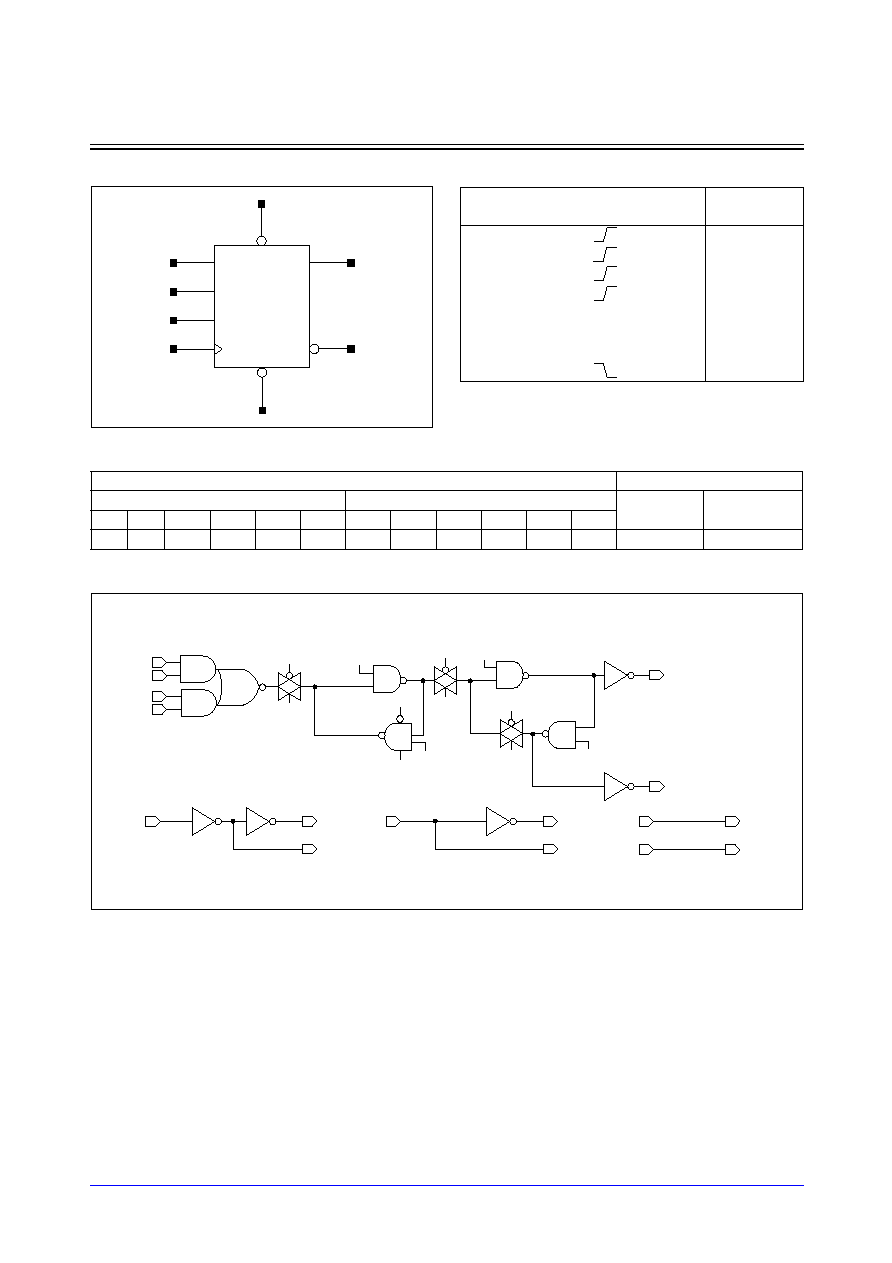
STDL131
3-248
Samsung ASIC
FD4S_LP/FD4SD2_LP
D Flip-Flop with Reset, Set, Scan, 1X/2X Drive
Logic Symbol
Cell Data
Schematic Diagram
Input Load (SL)
Gate Count
FD4S_LP
FD4SD2_LP
FD4S_LP
FD4SD2_LP
D
CK
RN
SN
TI
TE
D
CK
RN
SN
TI
TE
0.7
1.1
1.7
2.0
0.7
1.6
0.7
1.1
1.8
2.2
0.7
1.6
9.33
9.67
Q
QN
D
TI
TE
CK RN
SN
CL
CLB
CLB
CL
CLB
CL
CL
CLB
CK
CL
CLB
TE
TEB
TE
SN
RN
RN
RN
RN
SN
Q
QN
SN
SN
D
TE
TI
TEB
Truth Table
D
TI
TE
CK
RN
SN
Q
(n+1)
QN
(n+1)
0
x
0
1
1
0
1
1
x
0
1
1
1
0
x
0
1
1
1
0
1
x
1
1
1
1
1
0
x
x
x
x
1
0
1
0
x
x
x
x
0
1
0
1
x
x
x
x
0
0
0
0
x
x
x
1
1
Q (n) QN (n)

Samsung ASIC
3-249
STDL131
FD4S_LP/FD4SD2_LP
D Flip-Flop with Reset, Set, Scan, 1X/2X Drive
Timing Requirements
(Typical process, 25
∞
C, 1.8V, Unit = ns)
Parameter
Symbol
Value (ns)
FD4S_LP
FD4SD2_LP
Input Setup Time (D to CK)
t
SU
0.292
0.291
Input Hold Time (D to CK)
t
HD
0.010
0.010
Pulse Width Low (CK)
t
PWL
0.334
0.335
Pulse Width High (CK)
t
PWH
0.177
0.202
Pulse Width Low (RN)
t
PWL
0.238
0.278
Pulse Width Low (SN)
t
PWL
0.354
0.408
Recovery Time (RN to CK)
t
RC
0.010
0.010
Removal Time (RN to CK)
t
RM
0.925
0.926
Recovery Time (SN to CK)
t
RC
0.010
0.010
Removal Time (SN to CK)
t
RM
0.214
0.213
Input Setup Time (TI to CK)
t
SU
0.348
0.347
Input Hold Time (TI to CK)
t
HD
0.010
0.010
Input Setup Time (TE to CK)
t
SU
0.329
0.328
Input Hold Time (TE to CK)
t
HD
0.010
0.010
Recovery Time (SN to RN)
t
RC
0.010
0.010
Removal Time (SN to RN)
t
RM
0.060
0.056

STDL131
3-250
Samsung ASIC
FD4S_LP/FD4SD2_LP
D Flip-Flop with Reset, Set, Scan, 1X/2X Drive
Switching Characteristics
(Typical process, 25
∞
C, 1.8V, t
R
/t
F
= 0.19ns, SL: Standard Load)
FD4S_LP
Path
Parameter
Delay [ns]
SL = 2
Delay Equations [ns]
Group1*
Group2*
Group3*
CK to Q
tR
0.107
0.058 + 0.025*SL
0.054 + 0.025*SL
0.050 + 0.026*SL
tF
0.077
0.045 + 0.016*SL
0.043 + 0.017*SL
0.044 + 0.017*SL
tPLH
0.340
0.311 + 0.015*SL
0.317 + 0.013*SL
0.320 + 0.013*SL
tPHL
0.334
0.309 + 0.012*SL
0.317 + 0.010*SL
0.322 + 0.010*SL
RN to Q
tR
0.105
0.057 + 0.024*SL
0.053 + 0.025*SL
0.047 + 0.026*SL
tF
0.077
0.045 + 0.016*SL
0.043 + 0.017*SL
0.041 + 0.017*SL
tPLH
0.172
0.143 + 0.014*SL
0.149 + 0.013*SL
0.152 + 0.012*SL
tPHL
0.183
0.158 + 0.012*SL
0.165 + 0.010*SL
0.170 + 0.010*SL
SN to Q
tR
0.118
0.072 + 0.023*SL
0.067 + 0.025*SL
0.059 + 0.025*SL
tPLH
0.505
0.474 + 0.015*SL
0.483 + 0.013*SL
0.488 + 0.013*SL
CK to QN
tR
0.104
0.056 + 0.024*SL
0.053 + 0.025*SL
0.046 + 0.026*SL
tF
0.074
0.041 + 0.017*SL
0.042 + 0.016*SL
0.040 + 0.017*SL
tPLH
0.435
0.407 + 0.014*SL
0.412 + 0.013*SL
0.415 + 0.012*SL
tPHL
0.413
0.389 + 0.012*SL
0.396 + 0.010*SL
0.400 + 0.010*SL
RN to QN
tR
0.122
0.063 + 0.029*SL
0.073 + 0.027*SL
0.082 + 0.026*SL
tPLH
0.308
0.273 + 0.017*SL
0.280 + 0.016*SL
0.293 + 0.014*SL
SN to QN
tR
0.121
0.064 + 0.029*SL
0.071 + 0.027*SL
0.078 + 0.026*SL
tF
0.081
0.044 + 0.018*SL
0.049 + 0.017*SL
0.046 + 0.018*SL
tPLH
0.187
0.152 + 0.017*SL
0.159 + 0.016*SL
0.171 + 0.014*SL
tPHL
0.196
0.170 + 0.013*SL
0.178 + 0.011*SL
0.183 + 0.010*SL
*Group1 : SL < 4, *Group2 : 4 SL
<
<
=
= 8, *Group3 : 8 < SL
Samsung ASIC
3-251
STDL131
FD4S_LP/FD4SD2_LP
D Flip-Flop with Reset, Set, Scan, 1X/2X Drive
Switching Characteristics
(Typical process, 25
∞
C, 1.8V, t
R
/t
F
= 0.19ns, SL: Standard Load)
FD4SD2_LP
Path
Parameter
Delay [ns]
SL = 2
Delay Equations [ns]
Group1*
Group2*
Group3*
CK to Q
tR
0.084
0.060 + 0.012*SL
0.059 + 0.012*SL
0.055 + 0.013*SL
tF
0.064
0.046 + 0.009*SL
0.048 + 0.008*SL
0.048 + 0.008*SL
tPLH
0.349
0.330 + 0.009*SL
0.339 + 0.007*SL
0.348 + 0.006*SL
tPHL
0.344
0.328 + 0.008*SL
0.336 + 0.006*SL
0.347 + 0.005*SL
RN to Q
tR
0.083
0.059 + 0.012*SL
0.057 + 0.012*SL
0.053 + 0.013*SL
tF
0.063
0.044 + 0.009*SL
0.050 + 0.008*SL
0.046 + 0.008*SL
tPLH
0.176
0.158 + 0.009*SL
0.166 + 0.007*SL
0.176 + 0.006*SL
tPHL
0.188
0.172 + 0.008*SL
0.180 + 0.006*SL
0.191 + 0.005*SL
SN to Q
tR
0.097
0.072 + 0.012*SL
0.075 + 0.012*SL
0.066 + 0.012*SL
tPLH
0.549
0.528 + 0.010*SL
0.539 + 0.007*SL
0.552 + 0.006*SL
CK to QN
tR
0.079
0.054 + 0.012*SL
0.055 + 0.012*SL
0.047 + 0.013*SL
tF
0.061
0.042 + 0.009*SL
0.048 + 0.008*SL
0.044 + 0.008*SL
tPLH
0.463
0.446 + 0.009*SL
0.453 + 0.007*SL
0.461 + 0.006*SL
tPHL
0.453
0.438 + 0.008*SL
0.445 + 0.006*SL
0.456 + 0.005*SL
RN to QN
tR
0.088
0.060 + 0.014*SL
0.062 + 0.014*SL
0.072 + 0.013*SL
tPLH
0.324
0.304 + 0.010*SL
0.312 + 0.008*SL
0.324 + 0.007*SL
SN to QN
tR
0.086
0.058 + 0.014*SL
0.059 + 0.014*SL
0.069 + 0.013*SL
tF
0.065
0.045 + 0.010*SL
0.051 + 0.008*SL
0.050 + 0.009*SL
tPLH
0.175
0.155 + 0.010*SL
0.163 + 0.008*SL
0.174 + 0.007*SL
tPHL
0.198
0.182 + 0.008*SL
0.190 + 0.006*SL
0.201 + 0.005*SL
*Group1 : SL < 4, *Group2 : 4 SL
<
<
=
= 12, *Group3 : 12 < SL
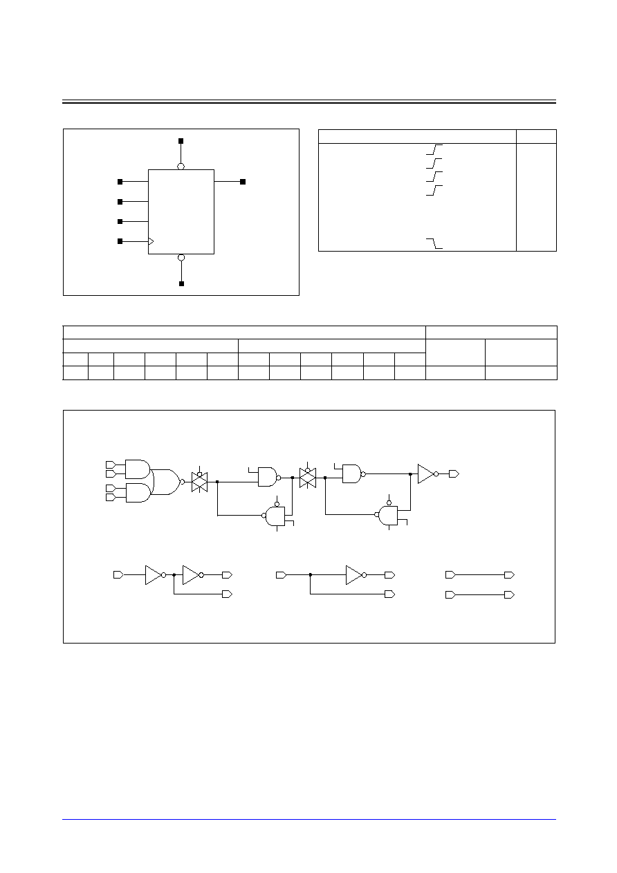
STDL131
3-252
Samsung ASIC
FD4SQ_LP/FD4SQD2_LP
D Flip-Flop with Reset, Set, Scan, Q Output Only, 1X/2X Drive
Logic Symbol
Cell Data
Schematic Diagram
Input Load (SL)
Gate Count
FD4SQ_LP
FD4SQD2_LP
FD4SQ_LP FD4SQD2_LP
D
CK
RN
SN
TI
TE
D
CK
RN
SN
TI
TE
0.7
1.1
1.6
1.4
0.7
1.7
0.7
1.1
1.6
1.4
0.7
1.6
8.00
8.33
Q
D
TI
TE
CK RN
SN
CL
CLB
CLB
CL
CLB
CL
CL
CLB
CK
CL
CLB
TE
TEB
TE
SN
RN
RN
RN
SN
Q
SN
RN
SN
D
TE
TI
TEB
Truth Table
D
TI
TE
CK
RN
SN
Q (n+1)
0
x
0
1
1
0
1
x
0
1
1
1
x
0
1
1
1
0
x
1
1
1
1
1
x
x
x
x
1
0
1
x
x
x
x
0
1
0
x
x
x
x
0
0
0
x
x
x
1
1
Q (n)
Samsung ASIC
3-253
STDL131
FD4SQ_LP/FD4SQD2_LP
D Flip-Flop with Reset, Set, Scan, Q Output Only, 1X/2X Drive
Timing Requirements
(Typical process, 25
∞
C, 1.8V, Unit = ns)
Parameter
Symbol
Value (ns)
FD4SQ_LP
FD4SQD2_LP
Input Setup Time (D to CK)
t
SU
0.293
0.293
Input Hold Time (D to CK)
t
HD
0.010
0.010
Pulse Width Low (CK)
t
PWL
0.336
0.336
Pulse Width High (CK)
t
PWH
0.146
0.153
Pulse Width Low (RN)
t
PWL
0.288
0.303
Pulse Width Low (SN)
t
PWL
1.003
1.033
Recovery Time (RN to CK)
t
RC
0.010
0.010
Removal Time (RN to CK)
t
RM
0.922
0.931
Recovery Time (SN to CK)
t
RC
0.010
0.010
Removal Time (SN to CK)
t
RM
0.214
0.217
Input Setup Time (TI to CK)
t
SU
0.348
0.346
Input Hold Time (TI to CK)
t
HD
0.010
0.010
Input Setup Time (TE to CK)
t
SU
0.332
0.329
Input Hold Time (TE to CK)
t
HD
0.010
0.010
Removal Time (SN to RN)
t
RM
0.061
0.061
Recovery Time (SN to RN)
t
RC
0.010
0.010
STDL131
3-254
Samsung ASIC
FD4SQ_LP/FD4SQD2_LP
D Flip-Flop with Reset, Set, Scan, Q Output Only, 1X/2X Drive
Switching Characteristics
(Typical process, 25
∞
C, 1.8V, t
R
/t
F
= 0.19ns, SL: Standard Load)
FD4SQ_LP
FD4SQD2_LP
Path
Parameter
Delay [ns]
SL = 2
Delay Equations [ns]
Group1*
Group2*
Group3*
CK to Q
tR
0.103
0.054 + 0.025*SL
0.050 + 0.026*SL
0.044 + 0.026*SL
tF
0.073
0.040 + 0.017*SL
0.042 + 0.016*SL
0.035 + 0.017*SL
tPLH
0.323
0.295 + 0.014*SL
0.300 + 0.013*SL
0.303 + 0.013*SL
tPHL
0.317
0.294 + 0.012*SL
0.300 + 0.010*SL
0.304 + 0.010*SL
RN to Q
tR
0.102
0.051 + 0.025*SL
0.050 + 0.026*SL
0.043 + 0.026*SL
tF
0.072
0.040 + 0.016*SL
0.039 + 0.017*SL
0.036 + 0.017*SL
tPLH
0.161
0.132 + 0.014*SL
0.137 + 0.013*SL
0.139 + 0.013*SL
tPHL
0.169
0.146 + 0.011*SL
0.152 + 0.010*SL
0.155 + 0.010*SL
SN to Q
tR
0.126
0.081 + 0.023*SL
0.075 + 0.024*SL
0.063 + 0.026*SL
tPLH
0.951
0.919 + 0.016*SL
0.930 + 0.013*SL
0.935 + 0.013*SL
*Group1 : SL < 4, *Group2 : 4 SL
<
<
=
= 8, *Group3 : 8 < SL
Path
Parameter
Delay [ns]
SL = 2
Delay Equations [ns]
Group1*
Group2*
Group3*
CK to Q
tR
0.078
0.055 + 0.012*SL
0.053 + 0.012*SL
0.045 + 0.013*SL
tF
0.058
0.041 + 0.009*SL
0.041 + 0.008*SL
0.042 + 0.008*SL
tPLH
0.327
0.309 + 0.009*SL
0.317 + 0.007*SL
0.325 + 0.006*SL
tPHL
0.323
0.308 + 0.008*SL
0.315 + 0.006*SL
0.325 + 0.005*SL
RN to Q
tR
0.078
0.053 + 0.012*SL
0.053 + 0.012*SL
0.047 + 0.013*SL
tF
0.058
0.040 + 0.009*SL
0.041 + 0.008*SL
0.042 + 0.008*SL
tPLH
0.163
0.145 + 0.009*SL
0.153 + 0.007*SL
0.161 + 0.006*SL
tPHL
0.173
0.158 + 0.008*SL
0.166 + 0.006*SL
0.175 + 0.005*SL
SN to Q
tR
0.104
0.079 + 0.012*SL
0.083 + 0.012*SL
0.073 + 0.012*SL
tPLH
0.969
0.947 + 0.011*SL
0.960 + 0.008*SL
0.975 + 0.006*SL
*Group1 : SL < 4, *Group2 : 4 SL
<
<
=
= 12, *Group3 : 12 < SL
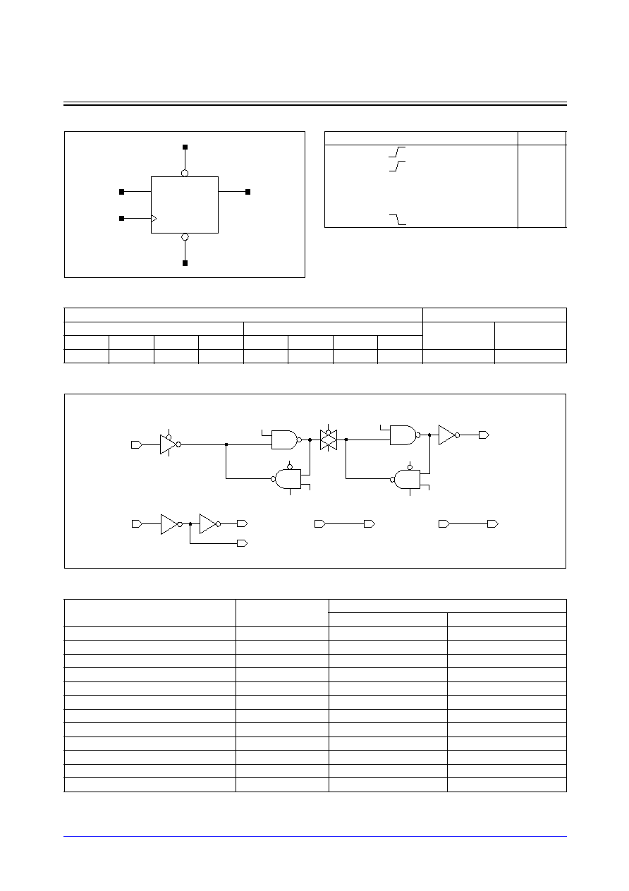
Samsung ASIC
3-255
STDL131
FD4Q_LP/FD4QD2_LP
D Flip-Flop with Reset, Set, Q Output Only, 1X/2X Drive
Logic Symbol
Cell Data
Schematic Diagram
Timing Requirements
(Typical process, 25
∞
C, 1.8V, Unit = ns)
Input Load (SL)
Gate Count
FD4Q_LP
FD4QD2_LP
FD4Q_LP
FD4QD2_LP
D
CK
RN
SN
D
CK
RN
SN
0.7
1.1
1.5
1.4
0.7
1.1
1.6
1.4
6.33
6.67
Parameter
Symbol
Value (ns)
FD4Q_LP
FD4QD2_LP
Input Setup Time (D to CK)
t
SU
0.137
0.137
Input Hold Time (D to CK)
t
HD
0.010
0.010
Pulse Width Low (CK)
t
PWL
0.231
0.232
Pulse Width High (CK)
t
PWH
0.146
0.152
Pulse Width Low (RN)
t
PWL
0.289
0.302
Pulse Width Low (SN)
t
PWL
1.003
1.030
Recovery Time (RN to CK)
t
RC
0.010
0.010
Removal Time (RN to CK)
t
RM
0.917
0.922
Recovery Time (SN to CK)
t
RC
0.010
0.010
Removal Time (SN to CK)
t
RM
0.215
0.216
Recovery Time (SN to RN)
t
RC
0.010
0.010
Removal Time (SN to RN)
t
RM
0.063
0.063
D
CK
Q
SN
RN
D
CK
CL
CLB
Q
CL
CLB
CL
CLB
CL
CL
CLB
CLB
SN
SN
RN
RN
RN
RN
SN
SN
Truth Table
D
CK
RN
SN
Q (n+1)
0
1
1
0
1
1
1
1
x
x
1
0
1
x
x
0
1
0
x
x
0
0
0
x
1
1
Q (n)

STDL131
3-256
Samsung ASIC
FD4Q_LP/FD4QD2_LP
D Flip-Flop with Reset, Set, Q Output Only, 1X/2X Drive
Switching Characteristics
(Typical process, 25
∞
C, 1.8V, t
R
/t
F
= 0.19ns, SL: Standard Load)
FD4Q_LP
FD4QD2_LP
Path
Parameter
Delay [ns]
SL = 2
Delay Equations [ns]
Group1*
Group2*
Group3*
CK to Q
tR
0.103
0.054 + 0.024*SL
0.049 + 0.025*SL
0.044 + 0.026*SL
tF
0.073
0.040 + 0.016*SL
0.041 + 0.016*SL
0.036 + 0.017*SL
tPLH
0.323
0.295 + 0.014*SL
0.300 + 0.013*SL
0.302 + 0.012*SL
tPHL
0.316
0.293 + 0.012*SL
0.299 + 0.010*SL
0.303 + 0.010*SL
RN to Q
tR
0.102
0.052 + 0.025*SL
0.050 + 0.025*SL
0.044 + 0.026*SL
tF
0.073
0.040 + 0.016*SL
0.039 + 0.017*SL
0.036 + 0.017*SL
tPLH
0.161
0.133 + 0.014*SL
0.138 + 0.013*SL
0.140 + 0.012*SL
tPHL
0.171
0.148 + 0.012*SL
0.154 + 0.010*SL
0.158 + 0.010*SL
SN to Q
tR
0.126
0.081 + 0.022*SL
0.076 + 0.024*SL
0.064 + 0.025*SL
tPLH
0.945
0.912 + 0.017*SL
0.926 + 0.013*SL
0.931 + 0.013*SL
*Group1 : SL < 4, *Group2 : 4 SL
<
<
=
= 8, *Group3 : 8 < SL
Path
Parameter
Delay [ns]
SL = 2
Delay Equations [ns]
Group1*
Group2*
Group3*
CK to Q
tR
0.079
0.055 + 0.012*SL
0.054 + 0.012*SL
0.046 + 0.013*SL
tF
0.058
0.041 + 0.008*SL
0.042 + 0.008*SL
0.041 + 0.008*SL
tPLH
0.325
0.308 + 0.009*SL
0.315 + 0.007*SL
0.323 + 0.006*SL
tPHL
0.320
0.305 + 0.007*SL
0.312 + 0.006*SL
0.322 + 0.005*SL
RN to Q
tR
0.079
0.055 + 0.012*SL
0.054 + 0.012*SL
0.048 + 0.013*SL
tF
0.059
0.041 + 0.009*SL
0.044 + 0.008*SL
0.041 + 0.008*SL
tPLH
0.162
0.145 + 0.009*SL
0.152 + 0.007*SL
0.160 + 0.006*SL
tPHL
0.173
0.158 + 0.007*SL
0.165 + 0.006*SL
0.174 + 0.005*SL
SN to Q
tR
0.105
0.081 + 0.012*SL
0.083 + 0.011*SL
0.074 + 0.012*SL
tPLH
0.959
0.936 + 0.012*SL
0.952 + 0.008*SL
0.967 + 0.006*SL
*Group1 : SL < 4, *Group2 : 4 SL
<
<
=
= 12, *Group3 : 12 < SL

Samsung ASIC
3-257
STDL131
FD5_LP/FD5D2_LP
D Flip-Flop with Negative Edge Trigger, 1X/2X Drive
Logic Symbol
Cell Data
Schematic Diagram
Timing Requirements
(Typical process, 25
∞
C, 1.8V, Unit = ns)
Input Load (SL)
Gate Count
FD5_LP
FD5D2_LP
FD5_LP
FD5D2_LP
D
CKN
D
CKN
0.7
1.1
0.7
1.1
5.67
5.67
Parameter
Symbol
Value (ns)
FD5_LP
FD5D2_LP
Input Setup Time (D to CKN)
t
SU
0.144
0.144
Input Hold Time (D to CKN)
t
HD
0.029
0.031
Pulse Width Low (CKN)
t
PWL
0.159
0.174
Pulse Width High (CKN)
t
PWH
0.159
0.174
D
CKN
Q
QN
CLN
CLBN
CLBN
CLN
CLN
CLBN
CLBN
CLN
D
CKN
CLN
CLBN
QN
Q
Truth Table
D
CKN
Q (n+1)
QN (n+1)
0
0
1
1
1
0
x
Q (n)
QN (n)

STDL131
3-258
Samsung ASIC
FD5_LP/FD5D2_LP
D Flip-Flop with Negative Edge Trigger, 1X/2X Drive
Switching Characteristics
(Typical process, 25
∞
C, 1.8V, t
R
/t
F
= 0.19ns, SL: Standard Load)
FD5_LP
FD5D2_LP
Path
Parameter
Delay [ns]
SL = 2
Delay Equations [ns]
Group1*
Group2*
Group3*
CKN to Q
tR
0.095
0.044 + 0.026*SL
0.042 + 0.026*SL
0.036 + 0.027*SL
tF
0.072
0.039 + 0.017*SL
0.036 + 0.017*SL
0.036 + 0.017*SL
tPLH
0.338
0.311 + 0.013*SL
0.314 + 0.013*SL
0.316 + 0.013*SL
tPHL
0.296
0.272 + 0.012*SL
0.278 + 0.010*SL
0.283 + 0.010*SL
CKN to QN
tR
0.093
0.042 + 0.026*SL
0.039 + 0.026*SL
0.035 + 0.027*SL
tF
0.070
0.036 + 0.017*SL
0.034 + 0.017*SL
0.033 + 0.017*SL
tPLH
0.355
0.329 + 0.013*SL
0.330 + 0.013*SL
0.331 + 0.013*SL
tPHL
0.394
0.371 + 0.011*SL
0.376 + 0.010*SL
0.379 + 0.010*SL
*Group1 : SL < 4, *Group2 : 4 SL
<
<
=
= 8, *Group3 : 8 < SL
Path
Parameter
Delay [ns]
SL = 2
Delay Equations [ns]
Group1*
Group2*
Group3*
CKN to Q
tR
0.069
0.044 + 0.012*SL
0.042 + 0.013*SL
0.036 + 0.013*SL
tF
0.056
0.039 + 0.009*SL
0.040 + 0.009*SL
0.041 + 0.008*SL
tPLH
0.342
0.326 + 0.008*SL
0.332 + 0.007*SL
0.336 + 0.006*SL
tPHL
0.302
0.286 + 0.008*SL
0.294 + 0.006*SL
0.304 + 0.005*SL
CKN to QN
tR
0.063
0.038 + 0.012*SL
0.036 + 0.013*SL
0.030 + 0.013*SL
tF
0.051
0.034 + 0.009*SL
0.036 + 0.008*SL
0.032 + 0.009*SL
tPLH
0.379
0.364 + 0.007*SL
0.367 + 0.006*SL
0.370 + 0.006*SL
tPHL
0.417
0.403 + 0.007*SL
0.409 + 0.005*SL
0.416 + 0.005*SL
*Group1 : SL < 4, *Group2 : 4 SL
<
<
=
= 12, *Group3 : 12 < SL
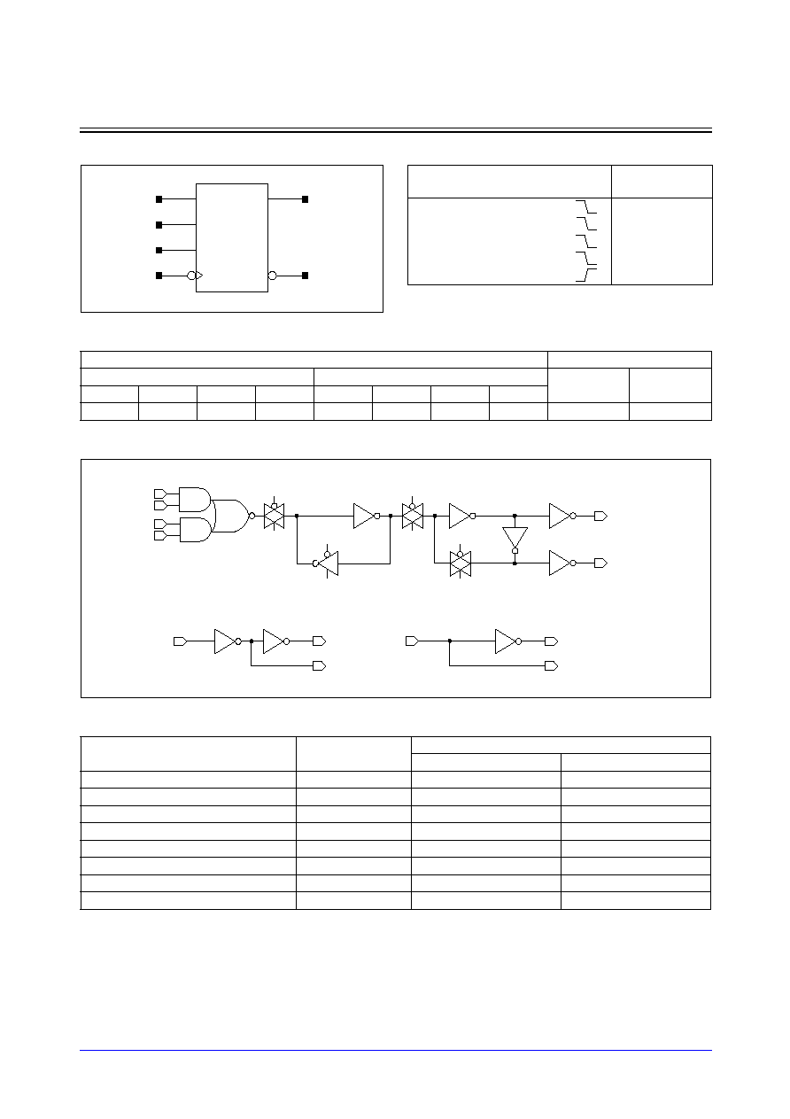
Samsung ASIC
3-259
STDL131
FD5S_LP/FD5SD2_LP
D Flip-Flop with Negative Edge Trigger, Scan, 1X/2X Drive
Logic Symbol
Cell Data
Schematic Diagram
Timing Requirements
(Typical process, 25
∞
C, 1.8V, Unit = ns)
Input Load (SL)
Gate Count
FD5S_LP
FD5SD2_LP
FD5S_LP
FD5SD2_LP
D
CKN
TI
TE
D
CKN
TI
TE
0.7
1.1
0.7
1.7
0.7
1.2
0.7
1.6
7.33
7.33
Parameter
Symbol
Value (ns)
FD5S_LP
FD5SD2_LP
Input Setup Time (D to CKN)
t
SU
0.340
0.340
Input Hold Time (D to CKN)
t
HD
0.010
0.010
Pulse Width Low (CKN)
t
PWL
0.159
0.175
Pulse Width High (CKN)
t
PWH
0.159
0.175
Input Setup Time (TI to CKN)
t
SU
0.393
0.391
Input Hold Time (TI to CKN)
t
HD
0.010
0.010
Input Setup Time (TE to CKN)
t
SU
0.374
0.373
Input Hold Time (TE to CKN)
t
HD
0.010
0.010
Q
QN
D
TI
TE
CKN
CLN
CLBN
CLBN
CLN
CLN
CLBN
CLN
CLBN
TE
TEB
TE
Q
QN
D
TE
TI
TEB
CLN
CLBN
CKN
Truth Table
D
TI
TE
CKN
Q
(n+1)
QN
(n+1)
0
x
0
0
1
1
x
0
1
0
x
0
1
0
1
x
1
1
1
0
x
x
x
Q (n)
QN (n)
STDL131
3-260
Samsung ASIC
FD5S_LP/FD5SD2_LP
D Flip-Flop with Negative Edge Trigger, Scan, 1X/2X Drive
Switching Characteristics
(Typical process, 25
∞
C, 1.8V, t
R
/t
F
= 0.19ns, SL: Standard Load)
FD5S_LP
FD5SD2_LP
Path
Parameter
Delay [ns]
SL = 2
Delay Equations [ns]
Group1*
Group2*
Group3*
CKN to Q
tR
0.095
0.045 + 0.025*SL
0.042 + 0.026*SL
0.038 + 0.026*SL
tF
0.071
0.037 + 0.017*SL
0.038 + 0.017*SL
0.036 + 0.017*SL
tPLH
0.339
0.312 + 0.013*SL
0.314 + 0.013*SL
0.316 + 0.012*SL
tPHL
0.294
0.271 + 0.012*SL
0.277 + 0.010*SL
0.281 + 0.010*SL
CKN to QN
tR
0.093
0.044 + 0.025*SL
0.038 + 0.026*SL
0.037 + 0.026*SL
tF
0.070
0.038 + 0.016*SL
0.037 + 0.017*SL
0.034 + 0.017*SL
tPLH
0.355
0.329 + 0.013*SL
0.331 + 0.013*SL
0.332 + 0.012*SL
tPHL
0.395
0.373 + 0.011*SL
0.378 + 0.010*SL
0.380 + 0.009*SL
*Group1 : SL < 4, *Group2 : 4 SL
<
<
=
= 8, *Group3 : 8 < SL
Path
Parameter
Delay [ns]
SL = 2
Delay Equations [ns]
Group1*
Group2*
Group3*
CKN to Q
tR
0.069
0.045 + 0.012*SL
0.042 + 0.013*SL
0.036 + 0.013*SL
tF
0.057
0.039 + 0.009*SL
0.041 + 0.008*SL
0.041 + 0.008*SL
tPLH
0.344
0.327 + 0.008*SL
0.333 + 0.007*SL
0.337 + 0.006*SL
tPHL
0.304
0.288 + 0.008*SL
0.296 + 0.006*SL
0.306 + 0.005*SL
CKN to QN
tR
0.063
0.038 + 0.012*SL
0.036 + 0.013*SL
0.030 + 0.013*SL
tF
0.053
0.036 + 0.009*SL
0.038 + 0.008*SL
0.032 + 0.009*SL
tPLH
0.381
0.366 + 0.007*SL
0.370 + 0.006*SL
0.372 + 0.006*SL
tPHL
0.418
0.404 + 0.007*SL
0.410 + 0.005*SL
0.417 + 0.005*SL
*Group1 : SL < 4, *Group2 : 4 SL
<
<
=
= 12, *Group3 : 12 < SL
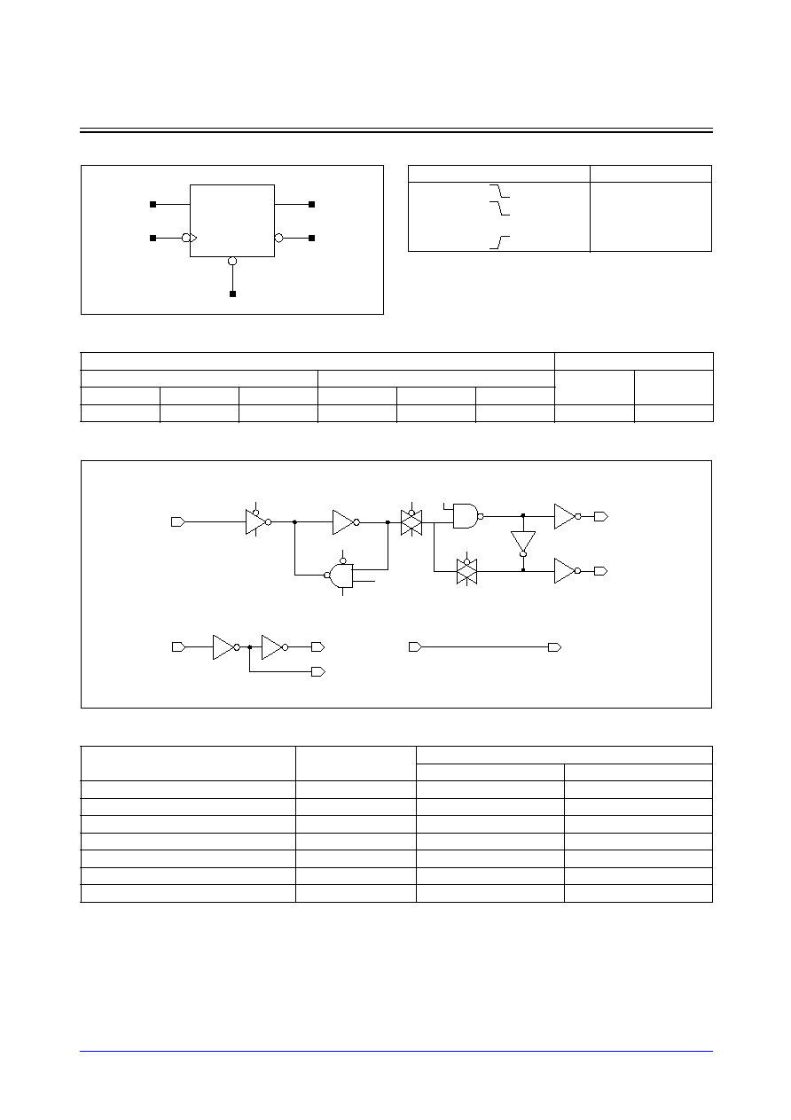
Samsung ASIC
3-261
STDL131
FD6_LP/FD6D2_LP
D Flip-Flop with Negative Edge Trigger, Reset, 1X/2X Drive
Logic Symbol
Cell Data
Schematic Diagram
Timing Requirements
(Typical process, 25
∞
C, 1.8V, Unit = ns)
Input Load (SL)
Gate Count
FD6_LP
FD6D2_LP
FD6_LP
FD6D2_LP
D
CKN
RN
D
CKN
RN
0.7
1.1
1.4
0.7
1.1
1.5
6.00
7.00
Parameter
Symbol
Value (ns)
FD6_LP
FD6D2_LP
Input Setup Time (D to CKN)
t
SU
0.147
0.148
Input Hold Time (D to CKN)
t
HD
0.027
0.028
Pulse Width Low (CKN)
t
PWL
0.165
0.197
Pulse Width High (CKN)
t
PWH
0.165
0.197
Pulse Width Low (RN)
t
PWL
0.896
0.902
Recovery Time (RN to CK)
t
RC
0.010
0.010
Removal Time (RN to CK)
t
RM
0.999
1.008
D
CKN
Q
QN
RN
CLN
CLBN
CLN
CLBN
D
CKN
CLN
CLBN
CLBN
CLN
RN
RN
QN
Q
RN
CLN
CLBN
RN
Truth Table
D
CKN
RN
Q (n+1) QN (n+1)
0
1
0
1
1
1
1
0
x
x
0
0
1
x
1
Q (n)
QN (n)

STDL131
3-262
Samsung ASIC
FD6_LP/FD6D2_LP
D Flip-Flop with Negative Edge Trigger, Reset, 1X/2X Drive
Switching Characteristics
(Typical process, 25
∞
C, 1.8V, t
R
/t
F
= 0.19ns, SL: Standard Load)
FD6_LP
FD6D2_LP
Path
Parameter
Delay [ns]
SL = 2
Delay Equations [ns]
Group1*
Group2*
Group3*
CKN to Q
tR
0.105
0.054 + 0.025*SL
0.052 + 0.026*SL
0.048 + 0.026*SL
tF
0.076
0.041 + 0.017*SL
0.044 + 0.017*SL
0.039 + 0.017*SL
tPLH
0.363
0.334 + 0.015*SL
0.340 + 0.013*SL
0.344 + 0.013*SL
tPHL
0.303
0.278 + 0.012*SL
0.285 + 0.011*SL
0.291 + 0.010*SL
RN to Q
tF
0.078
0.044 + 0.017*SL
0.043 + 0.017*SL
0.042 + 0.017*SL
tPHL
0.180
0.155 + 0.012*SL
0.162 + 0.011*SL
0.167 + 0.010*SL
CKN to QN
tR
0.091
0.041 + 0.025*SL
0.038 + 0.026*SL
0.032 + 0.027*SL
tF
0.069
0.036 + 0.017*SL
0.036 + 0.017*SL
0.032 + 0.017*SL
tPLH
0.361
0.335 + 0.013*SL
0.336 + 0.013*SL
0.338 + 0.013*SL
tPHL
0.419
0.396 + 0.011*SL
0.402 + 0.010*SL
0.404 + 0.010*SL
RN to QN
tR
0.102
0.047 + 0.028*SL
0.049 + 0.027*SL
0.055 + 0.026*SL
tPLH
0.254
0.223 + 0.015*SL
0.227 + 0.014*SL
0.235 + 0.013*SL
*Group1 : SL < 4, *Group2 : 4 SL
<
<
=
= 8, *Group3 : 8 < SL
Path
Parameter
Delay [ns]
SL = 2
Delay Equations [ns]
Group1*
Group2*
Group3*
CKN to Q
tR
0.083
0.057 + 0.013*SL
0.060 + 0.012*SL
0.055 + 0.013*SL
tF
0.063
0.045 + 0.009*SL
0.047 + 0.008*SL
0.050 + 0.008*SL
tPLH
0.380
0.361 + 0.010*SL
0.370 + 0.007*SL
0.380 + 0.006*SL
tPHL
0.318
0.302 + 0.008*SL
0.310 + 0.006*SL
0.323 + 0.005*SL
RN to Q
tF
0.063
0.044 + 0.010*SL
0.049 + 0.008*SL
0.050 + 0.008*SL
tPHL
0.192
0.175 + 0.008*SL
0.184 + 0.006*SL
0.196 + 0.005*SL
CKN to QN
tR
0.067
0.044 + 0.012*SL
0.040 + 0.013*SL
0.034 + 0.013*SL
tF
0.057
0.041 + 0.008*SL
0.041 + 0.008*SL
0.035 + 0.008*SL
tPLH
0.400
0.385 + 0.007*SL
0.389 + 0.006*SL
0.391 + 0.006*SL
tPHL
0.463
0.449 + 0.007*SL
0.456 + 0.005*SL
0.463 + 0.005*SL
RN to QN
tR
0.073
0.047 + 0.013*SL
0.045 + 0.013*SL
0.050 + 0.013*SL
tPLH
0.286
0.269 + 0.008*SL
0.273 + 0.007*SL
0.280 + 0.007*SL
*Group1 : SL < 4, *Group2 : 4 SL
<
<
=
= 12, *Group3 : 12 < SL
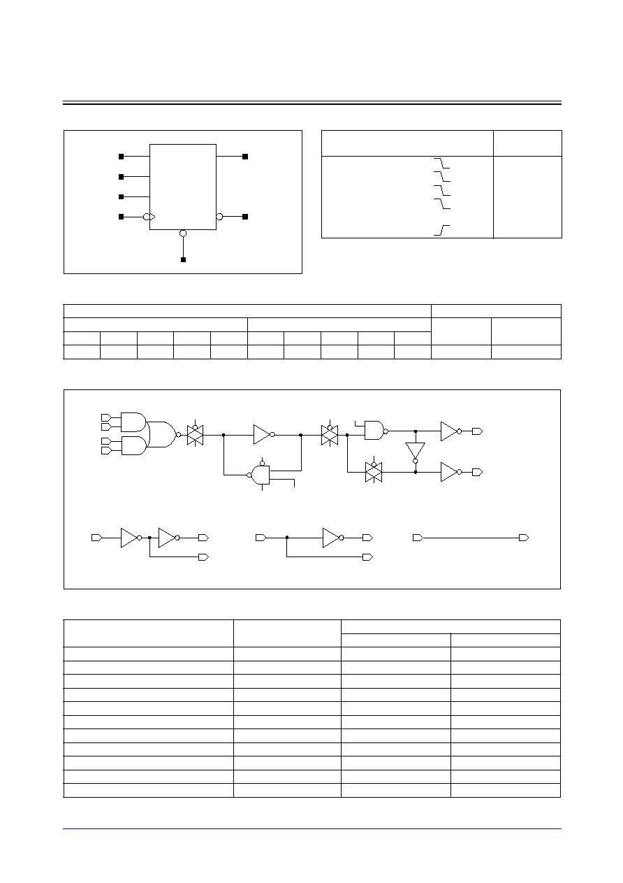
Samsung ASIC
3-263
STDL131
FD6S_LP/FD6SD2_LP
D Flip-Flop with Negative Edge Trigger, Reset, Scan, 1X/2X Drive
Logic Symbol
Cell Data
Schematic Diagram
Timing Requirements
(Typical process, 25
∞
C, 1.8V, Unit = ns)
Input Load (SL)
Gate Count
FD6S_LP
FD6SD2_LP
FD6S_LP
FD6SD2_LP
D
CKN
RN
TI
TE
D
CKN
RN
TI
TE
0.7
1.1
1.4
0.7
1.7
0.7
1.1
1.5
0.7
1.6
8.00
8.67
Parameter
Symbol
Value (ns)
FD6S_LP
FD6SD2_LP
Input Setup Time (D to CKN)
t
SU
0.341
0.341
Input Hold Time (D to CKN)
t
HD
0.010
0.010
Pulse Width Low (CKN)
t
PWL
0.168
0.201
Pulse Width High (CKN)
t
PWH
0.168
0.201
Pulse Width Low (RN)
t
PWL
0.911
0.918
Recovery Time (RN to CKN)
t
RC
0.010
0.010
Removal Time (RN to CKN)
t
RM
1.020
1.024
Input Setup Time (TI to CKN)
t
SU
0.404
0.393
Input Hold Time (TI to CKN)
t
HD
0.010
0.010
Input Setup Time (TE to CKN)
t
SU
0.395
0.374
Input Hold Time (TE to CKN)
t
HD
0.010
0.010
Q
QN
D
TI
TE
CKN RN
CLBN
CLN
CLN
CLBN
CLN
CLBN
CLN
CLBN
TE
TEB
TE
RN
RN
RN
QN
Q
CKN
D
TE
TI
TEB
CLN
CLBN
RN
Truth Table
D
TI
TE
CKN
RN
Q
(n+1)
QN
(n+1)
0
x
0
1
0
1
1
x
0
1
1
0
x
0
1
1
0
1
x
1
1
1
1
0
x
x
x
x
0
0
1
x
x
x
1
Q (n) QN (n)

STDL131
3-264
Samsung ASIC
FD6S_LP/FD6SD2_LP
D Flip-Flop with Negative Edge Trigger, Reset, Scan, 1X/2X Drive
Switching Characteristics
(Typical process, 25
∞
C, 1.8V, t
R
/t
F
= 0.19ns, SL: Standard Load)
FD6S_LP
FD6SD2_LP
Path
Parameter
Delay [ns]
SL = 2
Delay Equations [ns]
Group1*
Group2*
Group3*
CKN to Q
tR
0.104
0.054 + 0.025*SL
0.051 + 0.026*SL
0.047 + 0.026*SL
tF
0.074
0.039 + 0.017*SL
0.040 + 0.017*SL
0.040 + 0.017*SL
tPLH
0.367
0.338 + 0.015*SL
0.344 + 0.013*SL
0.348 + 0.013*SL
tPHL
0.305
0.280 + 0.012*SL
0.288 + 0.011*SL
0.293 + 0.010*SL
RN to Q
tF
0.077
0.044 + 0.017*SL
0.042 + 0.017*SL
0.041 + 0.017*SL
tPHL
0.179
0.155 + 0.012*SL
0.162 + 0.011*SL
0.166 + 0.010*SL
CKN to QN
tR
0.090
0.040 + 0.025*SL
0.033 + 0.027*SL
0.033 + 0.027*SL
tF
0.070
0.037 + 0.017*SL
0.036 + 0.017*SL
0.032 + 0.017*SL
tPLH
0.364
0.337 + 0.013*SL
0.340 + 0.013*SL
0.340 + 0.013*SL
tPHL
0.423
0.401 + 0.011*SL
0.406 + 0.010*SL
0.409 + 0.010*SL
RN to QN
tR
0.102
0.047 + 0.028*SL
0.049 + 0.027*SL
0.054 + 0.027*SL
tPLH
0.254
0.223 + 0.015*SL
0.227 + 0.014*SL
0.234 + 0.013*SL
*Group1 : SL < 4, *Group2 : 4 SL
<
<
=
= 8, *Group3 : 8 < SL
Path
Parameter
Delay [ns]
SL = 2
Delay Equations [ns]
Group1*
Group2*
Group3*
CKN to Q
tR
0.083
0.057 + 0.013*SL
0.057 + 0.013*SL
0.054 + 0.013*SL
tF
0.062
0.044 + 0.009*SL
0.047 + 0.008*SL
0.049 + 0.008*SL
tPLH
0.389
0.369 + 0.010*SL
0.379 + 0.007*SL
0.389 + 0.007*SL
tPHL
0.322
0.305 + 0.008*SL
0.314 + 0.006*SL
0.327 + 0.005*SL
RN to Q
tF
0.063
0.044 + 0.009*SL
0.048 + 0.009*SL
0.051 + 0.008*SL
tPHL
0.191
0.174 + 0.008*SL
0.183 + 0.006*SL
0.195 + 0.005*SL
CKN to QN
tR
0.066
0.043 + 0.011*SL
0.038 + 0.013*SL
0.031 + 0.013*SL
tF
0.056
0.038 + 0.009*SL
0.041 + 0.008*SL
0.036 + 0.008*SL
tPLH
0.403
0.388 + 0.008*SL
0.392 + 0.006*SL
0.395 + 0.006*SL
tPHL
0.472
0.458 + 0.007*SL
0.465 + 0.006*SL
0.472 + 0.005*SL
RN to QN
tR
0.072
0.046 + 0.013*SL
0.043 + 0.014*SL
0.047 + 0.013*SL
tPLH
0.285
0.268 + 0.008*SL
0.272 + 0.007*SL
0.279 + 0.007*SL
*Group1 : SL < 4, *Group2 : 4 SL
<
<
=
= 12, *Group3 : 12 < SL
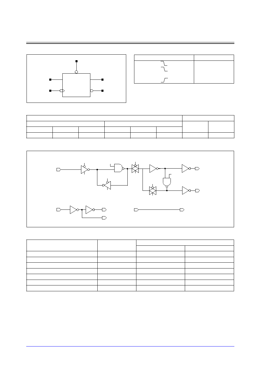
Samsung ASIC
3-265
STDL131
FD7_LP/FD7D2_LP
D Flip-Flop with Negative Edge Trigger, Set, 1X/2X Drive
Logic Symbol
Cell Data
Schematic Diagram
Timing Requirements
(Typical process, 25
∞
C, 1.8V, Unit = ns)
Input Load (SL)
Gate Count
FD7_LP
FD7D2_LP
FD7_LP
FD7D2_LP
D
CKN
SN
D
CKN
SN
0.7
1.1
2.0
0.7
1.1
2.1
6.67
7.00
Parameter
Symbol
Value (ns)
FD7_LP
FD7D2_LP
Input Setup Time (D to CKN)
t
SU
0.166
0.166
Input Hold Time (D to CKN)
t
HD
0.031
0.033
Pulse Width Low (CKN)
t
PWL
0.173
0.186
Pulse Width High (CKN)
t
PWH
0.173
0.186
Pulse Width Low (SN)
t
PWL
0.222
0.219
Recovery Time (SN to CKN)
t
RC
0.010
0.010
Removal Time (SN to CKN)
t
RM
0.146
0.143
D
CKN
Q
QN
SN
CLN
CLBN
CLN
CLBN
CLBN
CLN
D
CKN
CLN
CLBN
CLBN
CLN
SN
SN
SN
QN
Q
SN
Truth Table
D
CKN
SN
Q (n+1) QN (n+1)
0
1
0
1
1
1
1
0
x
x
0
1
0
x
1
Q (n)
QN (n)

STDL131
3-266
Samsung ASIC
FD7_LP/FD7D2_LP
D Flip-Flop with Negative Edge Trigger, Set, 1X/2X Drive
Switching Characteristics
(Typical process, 25
∞
C, 1.8V, t
R
/t
F
= 0.19ns, SL: Standard Load)
FD7_LP
FD7D2_LP
Path
Parameter
Delay [ns]
SL = 2
Delay Equations [ns]
Group1*
Group2*
Group3*
CKN to Q
tR
0.095
0.045 + 0.025*SL
0.042 + 0.026*SL
0.036 + 0.027*SL
tF
0.074
0.042 + 0.016*SL
0.037 + 0.017*SL
0.037 + 0.017*SL
tPLH
0.341
0.314 + 0.014*SL
0.317 + 0.013*SL
0.319 + 0.013*SL
tPHL
0.312
0.288 + 0.012*SL
0.294 + 0.010*SL
0.298 + 0.010*SL
SN to Q
tR
0.110
0.064 + 0.023*SL
0.056 + 0.025*SL
0.047 + 0.026*SL
tPLH
0.471
0.442 + 0.015*SL
0.449 + 0.013*SL
0.451 + 0.013*SL
CKN to QN
tR
0.105
0.055 + 0.025*SL
0.052 + 0.026*SL
0.047 + 0.026*SL
tF
0.074
0.040 + 0.017*SL
0.043 + 0.017*SL
0.037 + 0.017*SL
tPLH
0.412
0.384 + 0.014*SL
0.389 + 0.013*SL
0.392 + 0.013*SL
tPHL
0.413
0.389 + 0.012*SL
0.396 + 0.010*SL
0.400 + 0.010*SL
SN to QN
tF
0.083
0.047 + 0.018*SL
0.050 + 0.018*SL
0.047 + 0.018*SL
tPHL
0.197
0.171 + 0.013*SL
0.179 + 0.011*SL
0.184 + 0.011*SL
*Group1 : SL < 4, *Group2 : 4 SL
<
<
=
= 8, *Group3 : 8 < SL
Path
Parameter
Delay [ns]
SL = 2
Delay Equations [ns]
Group1*
Group2*
Group3*
CKN to Q
tR
0.069
0.044 + 0.012*SL
0.043 + 0.013*SL
0.037 + 0.013*SL
tF
0.059
0.042 + 0.009*SL
0.044 + 0.008*SL
0.041 + 0.008*SL
tPLH
0.344
0.328 + 0.008*SL
0.334 + 0.007*SL
0.337 + 0.006*SL
tPHL
0.318
0.303 + 0.008*SL
0.311 + 0.006*SL
0.320 + 0.005*SL
SN to Q
tR
0.087
0.064 + 0.012*SL
0.064 + 0.012*SL
0.050 + 0.013*SL
tPLH
0.502
0.483 + 0.009*SL
0.493 + 0.007*SL
0.501 + 0.006*SL
CKN to QN
tR
0.077
0.052 + 0.012*SL
0.051 + 0.012*SL
0.045 + 0.013*SL
tF
0.058
0.039 + 0.009*SL
0.044 + 0.008*SL
0.041 + 0.008*SL
tPLH
0.435
0.417 + 0.009*SL
0.425 + 0.007*SL
0.432 + 0.006*SL
tPHL
0.437
0.422 + 0.008*SL
0.430 + 0.006*SL
0.439 + 0.005*SL
SN to QN
tF
0.065
0.047 + 0.009*SL
0.048 + 0.009*SL
0.047 + 0.009*SL
tPHL
0.194
0.177 + 0.008*SL
0.185 + 0.006*SL
0.196 + 0.005*SL
*Group1 : SL < 4, *Group2 : 4 SL
<
<
=
= 12, *Group3 : 12 < SL
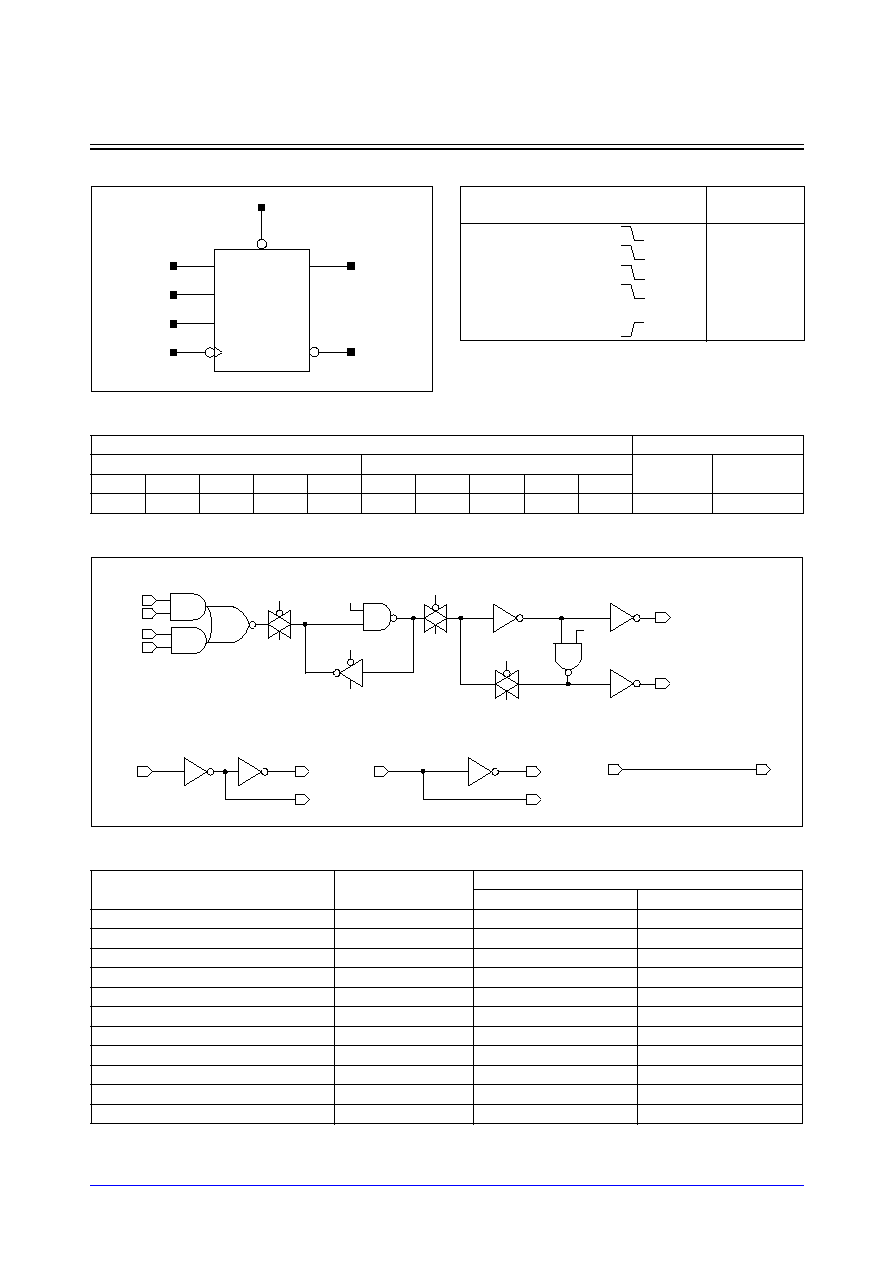
Samsung ASIC
3-267
STDL131
FD7S_LP/FD7SD2_LP
D Flip-Flop with Negative Edge Trigger, Set, Scan, 1X/2X Drive
Logic Symbol
Cell Data
Schematic Diagram
Timing Requirements
(Typical process, 25
∞
C, 1.8V, Unit = ns)
Input Load (SL)
Gate Count
FD7S_LP
FD7SD2_LP
FD7S_LP FD7SD2_LP
D
CKN
SN
TI
TE
D
CKN
SN
TI
TE
0.7
1.1
2.0
0.7
1.6
0.7
1.1
2.1
0.7
1.7
8.67
9.00
Parameter
Symbol
Value (ns)
FD7S_LP
FD7SD2_LP
Input Setup Time (D to CKN)
t
SU
0.356
0.355
Input Hold Time (D to CKN)
t
HD
0.010
0.010
Pulse Width Low (CKN)
t
PWL
0.171
0.185
Pulse Width High (CKN)
t
PWH
0.171
0.185
Pulse Width Low (SN)
t
PWL
0.220
0.218
Recovery Time (SN to CKN)
t
RC
0.010
0.010
Removal Time (SN to CKN)
t
RM
0.143
0.141
Input Setup Time (TI to CKN)
t
SU
0.410
0.410
Input Hold Time (TI to CKN)
t
HD
0.010
0.010
Input Setup Time (TE to CKN)
t
SU
0.393
0.393
Input Hold Time (TE to CKN)
t
HD
0.010
0.010
Q
QN
D
TI
TE
CKN
SN
CLBN
CLN
QN
CLN
CLBN
CLN
CLBN
Q
CKN
CLN
CLBN
TE
TEB
TE
SN
SN
SN
D
TE
TI
TEB
CLN
CLBN
SN
Truth Table
D
TI
TE
CKN
SN
Q
(n+1)
QN
(n+1)
0
x
0
1
0
1
1
x
0
1
1
0
x
0
1
1
0
1
x
1
1
1
1
0
x
x
x
x
0
1
0
x
x
x
1
Q (n) QN (n)

STDL131
3-268
Samsung ASIC
FD7S_LP/FD7SD2_LP
D Flip-Flop with Negative Edge Trigger, Set, Scan, 1X/2X Drive
Switching Characteristics
(Typical process, 25
∞
C, 1.8V, t
R
/t
F
= 0.19ns, SL: Standard Load)
FD7S_LP
FD7SD2_LP
Path
Parameter
Delay [ns]
SL = 2
Delay Equations [ns]
Group1*
Group2*
Group3*
CKN to Q
tR
0.095
0.045 + 0.025*SL
0.041 + 0.026*SL
0.038 + 0.027*SL
tF
0.074
0.041 + 0.017*SL
0.040 + 0.017*SL
0.038 + 0.017*SL
tPLH
0.343
0.316 + 0.014*SL
0.319 + 0.013*SL
0.320 + 0.013*SL
tPHL
0.311
0.287 + 0.012*SL
0.294 + 0.010*SL
0.298 + 0.010*SL
SN to Q
tR
0.110
0.064 + 0.023*SL
0.055 + 0.025*SL
0.047 + 0.026*SL
tPLH
0.469
0.440 + 0.015*SL
0.447 + 0.013*SL
0.448 + 0.013*SL
CKN to QN
tR
0.102
0.053 + 0.025*SL
0.048 + 0.026*SL
0.043 + 0.027*SL
tF
0.074
0.041 + 0.016*SL
0.041 + 0.017*SL
0.037 + 0.017*SL
tPLH
0.410
0.381 + 0.014*SL
0.387 + 0.013*SL
0.389 + 0.013*SL
tPHL
0.413
0.389 + 0.012*SL
0.395 + 0.010*SL
0.400 + 0.010*SL
SN to QN
tF
0.082
0.048 + 0.017*SL
0.046 + 0.018*SL
0.044 + 0.018*SL
tPHL
0.195
0.169 + 0.013*SL
0.177 + 0.011*SL
0.182 + 0.011*SL
*Group1 : SL < 4, *Group2 : 4 SL
<
<
=
= 8, *Group3 : 8 < SL
Path
Parameter
Delay [ns]
SL = 2
Delay Equations [ns]
Group1*
Group2*
Group3*
CKN to Q
tR
0.069
0.045 + 0.012*SL
0.043 + 0.013*SL
0.037 + 0.013*SL
tF
0.059
0.041 + 0.009*SL
0.045 + 0.008*SL
0.041 + 0.008*SL
tPLH
0.345
0.329 + 0.008*SL
0.335 + 0.007*SL
0.338 + 0.006*SL
tPHL
0.318
0.302 + 0.008*SL
0.310 + 0.006*SL
0.320 + 0.005*SL
SN to Q
tR
0.088
0.066 + 0.011*SL
0.062 + 0.012*SL
0.051 + 0.013*SL
tPLH
0.504
0.485 + 0.009*SL
0.495 + 0.007*SL
0.503 + 0.006*SL
CKN to QN
tR
0.076
0.051 + 0.012*SL
0.051 + 0.012*SL
0.044 + 0.013*SL
tF
0.058
0.039 + 0.010*SL
0.044 + 0.008*SL
0.041 + 0.008*SL
tPLH
0.433
0.416 + 0.009*SL
0.423 + 0.007*SL
0.431 + 0.006*SL
tPHL
0.439
0.424 + 0.008*SL
0.432 + 0.006*SL
0.441 + 0.005*SL
SN to QN
tF
0.065
0.045 + 0.010*SL
0.050 + 0.009*SL
0.046 + 0.009*SL
tPHL
0.194
0.177 + 0.008*SL
0.186 + 0.006*SL
0.197 + 0.005*SL
*Group1 : SL < 4, *Group2 : 4 SL
<
<
=
= 12, *Group3 : 12 < SL
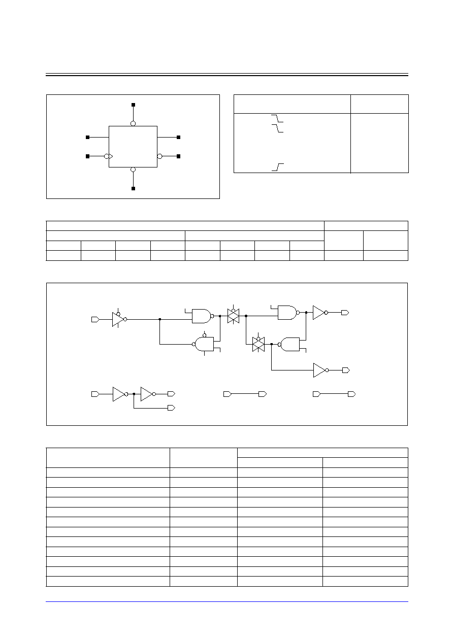
Samsung ASIC
3-269
STDL131
FD8_LP/FD8D2_LP
D Flip-Flop with Negative Edge Trigger, Reset, Set, 1X/2X Drive
Logic Symbol
Cell Data
Schematic Diagram
Timing Requirements
(Typical process, 25
∞
C, 1.8V, Unit = ns)
Input Load (SL)
Gate Count
FD8_LP
FD8D2_LP
FD8_LP
FD8D2_LP
D
CKN
RN
SN
D
CKN
RN
SN
0.7
1.1
1.7
2.0
0.7
1.1
1.8
2.2
7.67
8.00
Parameter
Symbol
Value (ns)
FD8_LP
FD8D2_LP
Input Setup Time (D to CKN)
t
SU
0.164
0.164
Input Hold Time (D to CKN)
t
HD
0.032
0.035
Pulse Width Low (CKN)
t
PWL
0.178
0.208
Pulse Width High (CKN)
t
PWH
0.178
0.208
Pulse Width Low (RN)
t
PWL
0.944
0.946
Pulse Width Low (SN)
t
PWL
0.274
0.274
Recovery Time (RN to CKN)
t
RC
0.010
0.010
Removal Time (RN to CKN)
t
RM
1.044
1.054
Recovery Time (SN to CKN)
t
RC
0.010
0.010
Removal Time (SN to CKN)
t
RM
0.189
0.188
Recovery Time (SN to RN)
t
RC
0.010
0.010
Removal Time (SN to RN)
t
RM
0.065
0.061
D
CKN
Q
QN
RN
SN
D
CKN
CLBN
CLN
Q
CLN
CLBN
CLBN
CLN
CLBN
CLBN
CLN
QN
CLN
SN
SN
RN
RN
RN
RN
SN
SN
Truth Table
D
CKN
RN
SN
Q
(n+1)
QN
(n+1)
0
1
1
0
1
1
1
1
1
0
x
x
1
0
1
0
x
x
0
1
0
1
x
x
0
0
0
0
x
1
1
Q (n)
QN (n)

STDL131
3-270
Samsung ASIC
FD8_LP/FD8D2_LP
D Flip-Flop with Negative Edge Trigger, Reset, Set, 1X/2X Drive
Switching Characteristics
(Typical process, 25
∞
C, 1.8V, t
R
/t
F
= 0.19ns, SL: Standard Load)
FD8_LP
Path
Parameter
Delay [ns]
SL = 2
Delay Equations [ns]
Group1*
Group2*
Group3*
CKN to Q
tR
0.106
0.057 + 0.025*SL
0.055 + 0.025*SL
0.050 + 0.026*SL
tF
0.077
0.044 + 0.016*SL
0.044 + 0.017*SL
0.043 + 0.017*SL
tPLH
0.376
0.347 + 0.015*SL
0.353 + 0.013*SL
0.357 + 0.013*SL
tPHL
0.327
0.303 + 0.012*SL
0.310 + 0.010*SL
0.315 + 0.010*SL
RN to Q
tR
0.106
0.057 + 0.024*SL
0.054 + 0.025*SL
0.047 + 0.026*SL
tF
0.076
0.042 + 0.017*SL
0.044 + 0.017*SL
0.040 + 0.017*SL
tPLH
0.172
0.143 + 0.015*SL
0.149 + 0.013*SL
0.152 + 0.012*SL
tPHL
0.183
0.159 + 0.012*SL
0.166 + 0.010*SL
0.170 + 0.010*SL
SN to Q
tR
0.118
0.072 + 0.023*SL
0.067 + 0.024*SL
0.060 + 0.025*SL
tPLH
0.507
0.476 + 0.015*SL
0.486 + 0.013*SL
0.490 + 0.013*SL
CKN to QN
tR
0.106
0.058 + 0.024*SL
0.052 + 0.025*SL
0.048 + 0.026*SL
tF
0.077
0.045 + 0.016*SL
0.044 + 0.016*SL
0.039 + 0.017*SL
tPLH
0.432
0.403 + 0.014*SL
0.409 + 0.013*SL
0.412 + 0.012*SL
tPHL
0.450
0.426 + 0.012*SL
0.433 + 0.010*SL
0.437 + 0.010*SL
RN to QN
tR
0.126
0.068 + 0.029*SL
0.076 + 0.027*SL
0.086 + 0.026*SL
tPLH
0.312
0.277 + 0.018*SL
0.284 + 0.016*SL
0.297 + 0.014*SL
SN to QN
tR
0.124
0.066 + 0.029*SL
0.074 + 0.027*SL
0.082 + 0.026*SL
tF
0.082
0.046 + 0.018*SL
0.050 + 0.017*SL
0.048 + 0.018*SL
tPLH
0.191
0.156 + 0.017*SL
0.163 + 0.016*SL
0.176 + 0.014*SL
tPHL
0.198
0.172 + 0.013*SL
0.180 + 0.011*SL
0.185 + 0.010*SL
*Group1 : SL < 4, *Group2 : 4 SL
<
<
=
= 8, *Group3 : 8 < SL

Samsung ASIC
3-271
STDL131
FD8_LP/FD8D2_LP
D Flip-Flop with Negative Edge Trigger, Reset, Set, 1X/2X Drive
Switching Characteristics
(Typical process, 25
∞
C, 1.8V, t
R
/t
F
= 0.19ns, SL: Standard Load)
FD8D2_LP
Path
Parameter
Delay [ns]
SL = 2
Delay Equations [ns]
Group1*
Group2*
Group3*
CKN to Q
tR
0.083
0.058 + 0.013*SL
0.059 + 0.012*SL
0.054 + 0.013*SL
tF
0.065
0.046 + 0.009*SL
0.050 + 0.008*SL
0.048 + 0.008*SL
tPLH
0.389
0.370 + 0.009*SL
0.378 + 0.007*SL
0.388 + 0.006*SL
tPHL
0.340
0.324 + 0.008*SL
0.332 + 0.006*SL
0.344 + 0.005*SL
RN to Q
tR
0.083
0.059 + 0.012*SL
0.057 + 0.012*SL
0.053 + 0.013*SL
tF
0.063
0.044 + 0.009*SL
0.050 + 0.008*SL
0.046 + 0.008*SL
tPLH
0.177
0.158 + 0.009*SL
0.167 + 0.007*SL
0.177 + 0.006*SL
tPHL
0.188
0.172 + 0.008*SL
0.180 + 0.006*SL
0.191 + 0.005*SL
SN to Q
tR
0.097
0.071 + 0.013*SL
0.076 + 0.012*SL
0.067 + 0.012*SL
tPLH
0.554
0.533 + 0.010*SL
0.544 + 0.007*SL
0.557 + 0.006*SL
CKN to QN
tR
0.079
0.054 + 0.012*SL
0.056 + 0.012*SL
0.047 + 0.013*SL
tF
0.062
0.045 + 0.008*SL
0.045 + 0.008*SL
0.045 + 0.008*SL
tPLH
0.461
0.444 + 0.009*SL
0.451 + 0.007*SL
0.459 + 0.006*SL
tPHL
0.494
0.479 + 0.008*SL
0.486 + 0.006*SL
0.497 + 0.005*SL
RN to QN
tR
0.089
0.060 + 0.014*SL
0.063 + 0.014*SL
0.072 + 0.013*SL
tPLH
0.327
0.306 + 0.010*SL
0.314 + 0.008*SL
0.326 + 0.007*SL
SN to QN
tR
0.085
0.055 + 0.015*SL
0.061 + 0.014*SL
0.069 + 0.013*SL
tF
0.067
0.048 + 0.009*SL
0.050 + 0.009*SL
0.050 + 0.009*SL
tPLH
0.177
0.157 + 0.010*SL
0.164 + 0.008*SL
0.176 + 0.007*SL
tPHL
0.200
0.183 + 0.008*SL
0.191 + 0.006*SL
0.202 + 0.005*SL
*Group1 : SL < 4, *Group2 : 4 SL
<
<
=
= 12, *Group3 : 12 < SL
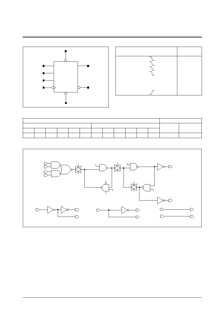
STDL131
3-272
Samsung ASIC
FD8S_LP/FD8SD2_LP
D Flip-Flop with Negative Edge Trigger, Reset, Set, Scan, 1X/2X Drive
Logic Symbol
Cell Data
Schematic Diagram
Input Load (SL)
Gate Count
FD8S_LP
FD8SD2_LP
FD8S_LP FD8SD2_LP
D
CKN
RN
SN
TI
TE
D
CKN
RN
SN
TI
TE
0.7
1.1
1.8
2.0
0.7
1.7
0.7
1.1
1.8
2.2
0.7
1.7
10.00
10.33
Q
QN
D
TI
TE
CKN RN
SN
CLBN
CLN
CLN
CLBN
CLN
CLBN
CLBN
CLN
CKN
CLN
CLBN
TE
TEB
TE
SN
RN
RN
SN
Q
QN
D
TE
TI
TEB
SN
SN
RN
RN
Truth Table
D
TI
TE
CKN RN
SN
Q
(n+1)
QN
(n+1)
0
x
0
1
1
0
1
1
x
0
1
1
1
0
x
0
1
1
1
0
1
x
1
1
1
1
1
0
x
x
x
x
1
0
1
0
x
x
x
x
0
1
0
1
x
x
x
x
0
0
0
0
x
x
x
1
1
Q (n) QN (n)
Samsung ASIC
3-273
STDL131
FD8S_LP/FD8SD2_LP
D Flip-Flop with Negative Edge Trigger, Reset, Set, Scan, 1X/2X Drive
Timing Requirements
(Typical process, 25
∞
C, 1.8V, Unit = ns)
Parameter
Symbol
Value (ns)
FD8S_LP
FD8SD2_LP
Input Setup Time (D to CKN)
t
SU
0.354
0.355
Input Hold Time (D to CKN)
t
HD
0.010
0.010
Pulse Width Low (CKN)
t
PWL
0.181
0.206
Pulse Width High (CKN)
t
PWH
0.181
0.206
Pulse Width Low (RN)
t
PWL
0.942
0.950
Pulse Width Low (SN)
t
PWL
0.271
0.271
Recovery Time (RN to CKN)
t
RC
0.010
0.010
Removal Time (RN to CKN)
t
RM
1.052
1.064
Recovery Time (SN to CKN)
t
RC
0.010
0.010
Removal Time (SN to CKN)
t
RM
0.186
0.187
Input Setup Time (TI to CKN)
t
SU
0.409
0.411
Input Hold Time (TI to CKN)
t
HD
0.010
0.010
Input Setup Time (TE to CKN)
t
SU
0.392
0.394
Input Hold Time (TE to CKN)
t
HD
0.010
0.010
Recovery Time (SN to RN)
t
RC
0.010
0.010
Removal Time (SN to RN)
t
RM
0.060
0.059

STDL131
3-274
Samsung ASIC
FD8S_LP/FD8SD2_LP
D Flip-Flop with Negative Edge Trigger, Reset, Set, Scan, 1X/2X Drive
Switching Characteristics
(Typical process, 25
∞
C, 1.8V, t
R
/t
F
= 0.19ns, SL: Standard Load)
FD8S_LP
Path
Parameter
Delay [ns]
SL = 2
Delay Equations [ns]
Group1*
Group2*
Group3*
CKN to Q
tR
0.107
0.058 + 0.025*SL
0.055 + 0.025*SL
0.051 + 0.026*SL
tF
0.078
0.045 + 0.016*SL
0.044 + 0.017*SL
0.043 + 0.017*SL
tPLH
0.381
0.351 + 0.015*SL
0.358 + 0.013*SL
0.361 + 0.013*SL
tPHL
0.331
0.306 + 0.012*SL
0.314 + 0.010*SL
0.319 + 0.010*SL
RN to Q
tR
0.106
0.058 + 0.024*SL
0.052 + 0.025*SL
0.048 + 0.026*SL
tF
0.076
0.042 + 0.017*SL
0.043 + 0.017*SL
0.040 + 0.017*SL
tPLH
0.172
0.143 + 0.015*SL
0.150 + 0.013*SL
0.152 + 0.012*SL
tPHL
0.183
0.159 + 0.012*SL
0.166 + 0.010*SL
0.170 + 0.010*SL
SN to Q
tR
0.120
0.073 + 0.023*SL
0.068 + 0.024*SL
0.060 + 0.025*SL
tPLH
0.519
0.488 + 0.016*SL
0.497 + 0.013*SL
0.501 + 0.013*SL
CKN to QN
tR
0.105
0.056 + 0.024*SL
0.053 + 0.025*SL
0.047 + 0.026*SL
tF
0.076
0.043 + 0.017*SL
0.044 + 0.016*SL
0.041 + 0.017*SL
tPLH
0.437
0.408 + 0.014*SL
0.414 + 0.013*SL
0.417 + 0.012*SL
tPHL
0.457
0.433 + 0.012*SL
0.440 + 0.010*SL
0.445 + 0.010*SL
RN to QN
tR
0.124
0.066 + 0.029*SL
0.073 + 0.027*SL
0.082 + 0.026*SL
tPLH
0.313
0.278 + 0.018*SL
0.285 + 0.016*SL
0.297 + 0.014*SL
SN to QN
tR
0.121
0.063 + 0.029*SL
0.072 + 0.027*SL
0.081 + 0.026*SL
tF
0.084
0.050 + 0.017*SL
0.049 + 0.017*SL
0.046 + 0.018*SL
tPLH
0.192
0.157 + 0.017*SL
0.164 + 0.016*SL
0.176 + 0.014*SL
tPHL
0.202
0.175 + 0.013*SL
0.183 + 0.011*SL
0.189 + 0.010*SL
*Group1 : SL < 4, *Group2 : 4 SL
<
<
=
= 8, *Group3 : 8 < SL

Samsung ASIC
3-275
STDL131
FD8S_LP/FD8SD2_LP
D Flip-Flop with Negative Edge Trigger, Reset, Set, Scan, 1X/2X Drive
Switching Characteristics
(Typical process, 25
∞
C, 1.8V, t
R
/t
F
= 0.19ns, SL: Standard Load)
FD8SD2_LP
Path
Parameter
Delay [ns]
SL = 2
Delay Equations [ns]
Group1*
Group2*
Group3*
CKN to Q
tR
0.084
0.059 + 0.012*SL
0.059 + 0.012*SL
0.054 + 0.013*SL
tF
0.064
0.046 + 0.009*SL
0.050 + 0.008*SL
0.049 + 0.008*SL
tPLH
0.389
0.370 + 0.009*SL
0.379 + 0.007*SL
0.388 + 0.006*SL
tPHL
0.339
0.323 + 0.008*SL
0.331 + 0.006*SL
0.343 + 0.005*SL
RN to Q
tR
0.082
0.058 + 0.012*SL
0.057 + 0.012*SL
0.053 + 0.013*SL
tF
0.063
0.044 + 0.009*SL
0.050 + 0.008*SL
0.045 + 0.008*SL
tPLH
0.176
0.158 + 0.009*SL
0.166 + 0.007*SL
0.176 + 0.006*SL
tPHL
0.188
0.172 + 0.008*SL
0.180 + 0.006*SL
0.191 + 0.005*SL
SN to Q
tR
0.097
0.071 + 0.013*SL
0.075 + 0.012*SL
0.065 + 0.012*SL
tPLH
0.550
0.529 + 0.010*SL
0.541 + 0.007*SL
0.554 + 0.006*SL
CKN to QN
tR
0.079
0.054 + 0.012*SL
0.055 + 0.012*SL
0.047 + 0.013*SL
tF
0.061
0.044 + 0.009*SL
0.047 + 0.008*SL
0.044 + 0.008*SL
tPLH
0.458
0.441 + 0.009*SL
0.448 + 0.007*SL
0.456 + 0.006*SL
tPHL
0.492
0.477 + 0.008*SL
0.485 + 0.006*SL
0.495 + 0.005*SL
RN to QN
tR
0.088
0.059 + 0.014*SL
0.061 + 0.014*SL
0.072 + 0.013*SL
tPLH
0.324
0.304 + 0.010*SL
0.311 + 0.008*SL
0.323 + 0.007*SL
SN to QN
tR
0.085
0.056 + 0.014*SL
0.059 + 0.014*SL
0.069 + 0.013*SL
tF
0.065
0.045 + 0.010*SL
0.051 + 0.008*SL
0.049 + 0.009*SL
tPLH
0.175
0.155 + 0.010*SL
0.162 + 0.008*SL
0.174 + 0.007*SL
tPHL
0.198
0.181 + 0.008*SL
0.189 + 0.006*SL
0.201 + 0.005*SL
*Group1 : SL < 4, *Group2 : 4 SL
<
<
=
= 12, *Group3 : 12 < SL
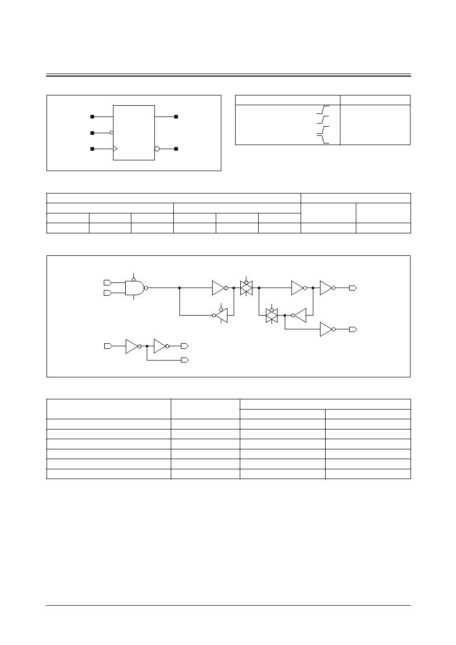
STDL131
3-276
Samsung ASIC
FDS2_LP/FDS2D2_LP
D Flip-Flop with Synchronous Clear, 1X/2X Drive
Logic Symbol
Cell Data
Schematic Diagram
Timing Requirements
(Typical process, 25
∞
C, 1.8V, Unit = ns)
Input Load (SL)
Gate Count
FDS2_LP
FDS2D2_LP
FDS2_LP
FDS2D2_LP
D
CRN
CK
D
CRN
CK
0.7
0.7
1.1
0.7
0.7
1.1
5.67
6.00
Parameter
Symbol
Value (ns)
FDS2_LP
FDS2D2_LP
Input Setup Time (D to CK)
t
SU
0.219
0.216
Input Hold Time (D to CK)
t
HD
0.010
0.010
Pulse Width Low (CK)
t
PWL
0.257
0.261
Pulse Width High (CK)
t
PWH
0.153
0.170
Input Setup Time (CRN to CK)
t
SU
0.220
0.220
Input Hold Time (CRN to CK)
t
HD
0.010
0.010
D
CRN
CK
Q
QN
D
CK
CL
CLB
Q
CL
CLB
CLB
CL
CLB
CL
CL
CLB
QN
CRN
Truth Table
D
CRN
CK
Q (n+1) QN (n+1)
0
1
0
1
1
1
1
0
x
0
0
1
x
x
Q (n)
QN (n)

Samsung ASIC
3-277
STDL131
FDS2_LP/FDS2D2_LP
D Flip-Flop with Synchronous Clear, 1X/2X Drive
Switching Characteristics
(Typical process, 25
∞
C, 1.8V, t
R
/t
F
= 0.19ns, SL: Standard Load)
FDS2_LP
FDS2D2_LP
Path
Parameter
Delay [ns]
SL = 2
Delay Equations [ns]
Group1*
Group2*
Group3*
CK to Q
tR
0.094
0.043 + 0.025*SL
0.039 + 0.027*SL
0.037 + 0.027*SL
tF
0.071
0.037 + 0.017*SL
0.038 + 0.017*SL
0.034 + 0.017*SL
tPLH
0.295
0.268 + 0.013*SL
0.271 + 0.013*SL
0.273 + 0.013*SL
tPHL
0.291
0.267 + 0.012*SL
0.273 + 0.010*SL
0.277 + 0.010*SL
CK to QN
tR
0.090
0.040 + 0.025*SL
0.034 + 0.027*SL
0.033 + 0.027*SL
tF
0.069
0.036 + 0.017*SL
0.035 + 0.017*SL
0.030 + 0.017*SL
tPLH
0.348
0.322 + 0.013*SL
0.324 + 0.013*SL
0.325 + 0.013*SL
tPHL
0.349
0.327 + 0.011*SL
0.332 + 0.010*SL
0.334 + 0.010*SL
*Group1 : SL < 4, *Group2 : 4 SL
<
<
=
= 8, *Group3 : 8 < SL
Path
Parameter
Delay [ns]
SL = 2
Delay Equations [ns]
Group1*
Group2*
Group3*
CK to Q
tR
0.070
0.045 + 0.012*SL
0.043 + 0.013*SL
0.036 + 0.013*SL
tF
0.058
0.042 + 0.008*SL
0.040 + 0.009*SL
0.042 + 0.008*SL
tPLH
0.305
0.288 + 0.008*SL
0.294 + 0.007*SL
0.298 + 0.006*SL
tPHL
0.306
0.290 + 0.008*SL
0.298 + 0.006*SL
0.307 + 0.005*SL
CK to QN
tR
0.064
0.040 + 0.012*SL
0.037 + 0.013*SL
0.031 + 0.013*SL
tF
0.053
0.036 + 0.008*SL
0.037 + 0.008*SL
0.032 + 0.009*SL
tPLH
0.383
0.368 + 0.007*SL
0.372 + 0.006*SL
0.374 + 0.006*SL
tPHL
0.379
0.365 + 0.007*SL
0.371 + 0.005*SL
0.379 + 0.005*SL
*Group1 : SL < 4, *Group2 : 4 SL
<
<
=
= 12, *Group3 : 12 < SL
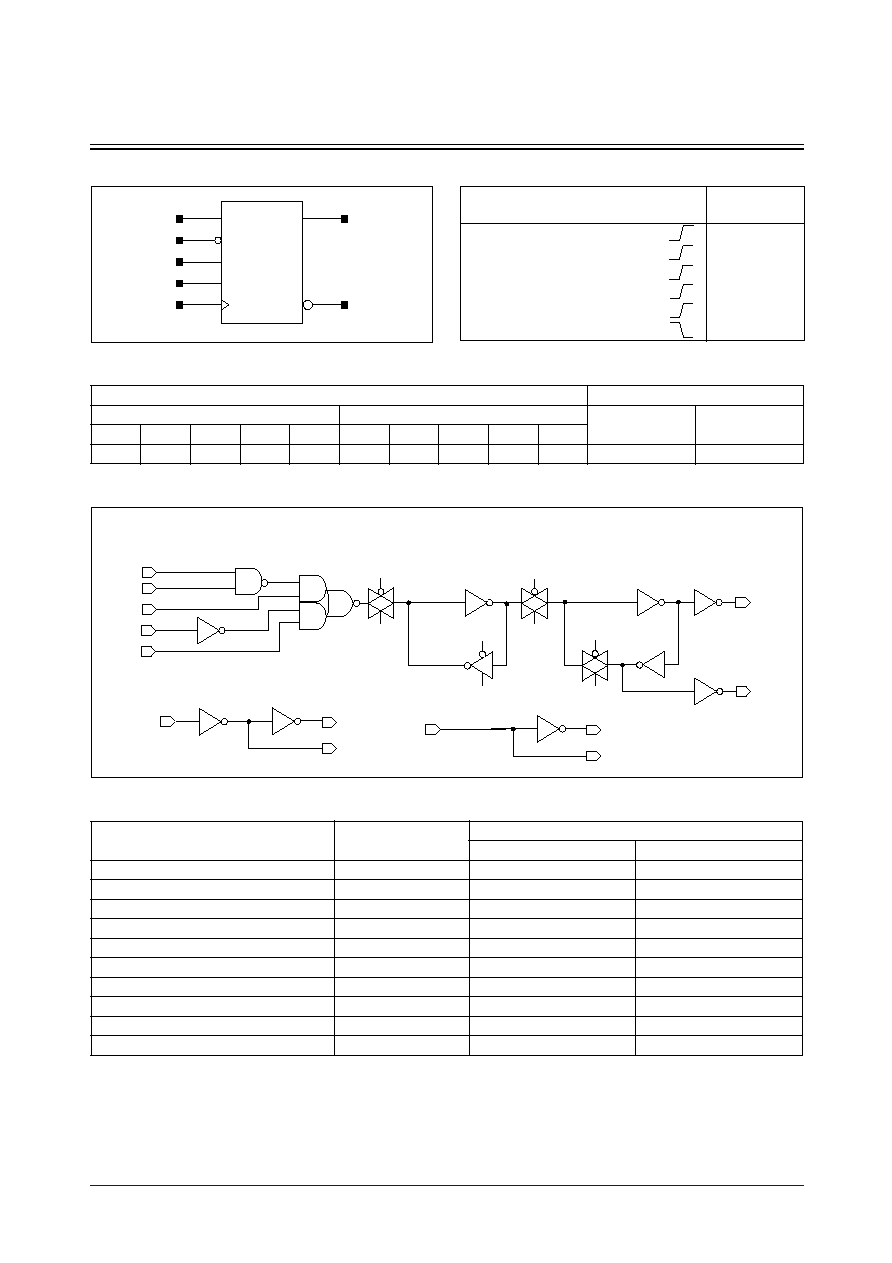
STDL131
3-278
Samsung ASIC
FDS2S_LP/FDS2SD2_LP
D Flip-Flop with Synchronous Clear, Scan, 1X/2X Drive
Logic Symbol
Cell Data
Schematic Diagram
Timing Requirements
(Typical process, 25
∞
C, 1.8V, Unit = ns)
Input Load (SL)
Gate Count
FDS2S_LP
FDS2SD2_LP
FDS2S_LP
FDS2SD2_LP
D
CRN
CK
TI
TE
D
CRN
CK
TI
TE
0.7
0.8
1.1
0.9
1.6
0.7
0.7
1.1
0.9
1.6
8.67
9.67
Parameter
Symbol
Value (ns)
FDS2S_LP
FDS2SD2_LP
Input Setup Time (D to CK)
t
SU
0.366
0.364
Input Hold Time (D to CK)
t
HD
0.010
0.010
Input Setup Time (CRN to CK)
t
SU
0.366
0.365
Input Hold Time (CRN to CK)
t
HD
0.010
0.010
Pulse Width Low (CK)
t
PWL
0.308
0.307
Pulse Width High (CK)
t
PWH
0.156
0.170
Input Setup Time (TI to CK)
t
SU
0.388
0.389
Input Hold Time (TI to CK)
t
HD
0.010
0.010
Input Setup Time (TE to CK)
t
SU
0.315
0.314
Input Hold Time (TE to CK)
t
HD
0.010
0.010
Q
QN
D
TE
CK
CRN
TI
QN
Q
CL
CLB
CL
CLB
CLB
CL
CRN
CL
CK
CLB
D
TI
TEB
TE
TE
TE
TEB
CL
CLB
Truth Table
D
CRN
TI
TE
CK
Q
(n+1)
QN
(n+1)
0
1
x
0
0
1
1
1
x
0
1
0
x
0
x
0
0
1
x
x
0
1
0
1
x
x
1
1
1
0
x
x
x
x
Q (n) QN (n)

Samsung ASIC
3-279
STDL131
FDS2S_LP/FDS2SD2_LP
D Flip-Flop with Synchronous Clear, Scan, 1X/2X Drive
Switching Characteristics
(Typical process, 25
∞
C, 1.8V, t
R
/t
F
= 0.19ns, SL: Standard Load)
FDS2S_LP
FDS2SD2_LP
Path
Parameter
Delay [ns]
SL = 2
Delay Equations [ns]
Group1*
Group2*
Group3*
CK to Q
tR
0.093
0.042 + 0.025*SL
0.040 + 0.026*SL
0.036 + 0.026*SL
tF
0.070
0.038 + 0.016*SL
0.036 + 0.017*SL
0.034 + 0.017*SL
tPLH
0.356
0.330 + 0.013*SL
0.332 + 0.013*SL
0.332 + 0.012*SL
tPHL
0.356
0.334 + 0.011*SL
0.339 + 0.010*SL
0.341 + 0.009*SL
CK to QN
tR
0.095
0.045 + 0.025*SL
0.042 + 0.026*SL
0.038 + 0.026*SL
tF
0.072
0.038 + 0.017*SL
0.038 + 0.017*SL
0.037 + 0.017*SL
tPLH
0.301
0.274 + 0.013*SL
0.277 + 0.013*SL
0.279 + 0.012*SL
tPHL
0.296
0.273 + 0.012*SL
0.279 + 0.010*SL
0.283 + 0.010*SL
*Group1 : SL < 4, *Group2 : 4 SL
<
<
=
= 8, *Group3 : 8 < SL
Path
Parameter
Delay [ns]
SL = 2
Delay Equations [ns]
Group1*
Group2*
Group3*
CK to Q
tR
0.066
0.043 + 0.012*SL
0.039 + 0.013*SL
0.033 + 0.013*SL
tF
0.053
0.036 + 0.009*SL
0.039 + 0.008*SL
0.036 + 0.008*SL
tPLH
0.381
0.367 + 0.007*SL
0.370 + 0.006*SL
0.372 + 0.006*SL
tPHL
0.380
0.366 + 0.007*SL
0.372 + 0.005*SL
0.379 + 0.005*SL
CK to QN
tR
0.070
0.047 + 0.012*SL
0.044 + 0.013*SL
0.038 + 0.013*SL
tF
0.058
0.043 + 0.008*SL
0.040 + 0.008*SL
0.043 + 0.008*SL
tPLH
0.305
0.289 + 0.008*SL
0.294 + 0.007*SL
0.298 + 0.006*SL
tPHL
0.303
0.288 + 0.008*SL
0.295 + 0.006*SL
0.304 + 0.005*SL
*Group1 : SL < 4, *Group2 : 4 SL
<
<
=
= 12, *Group3 : 12 < SL
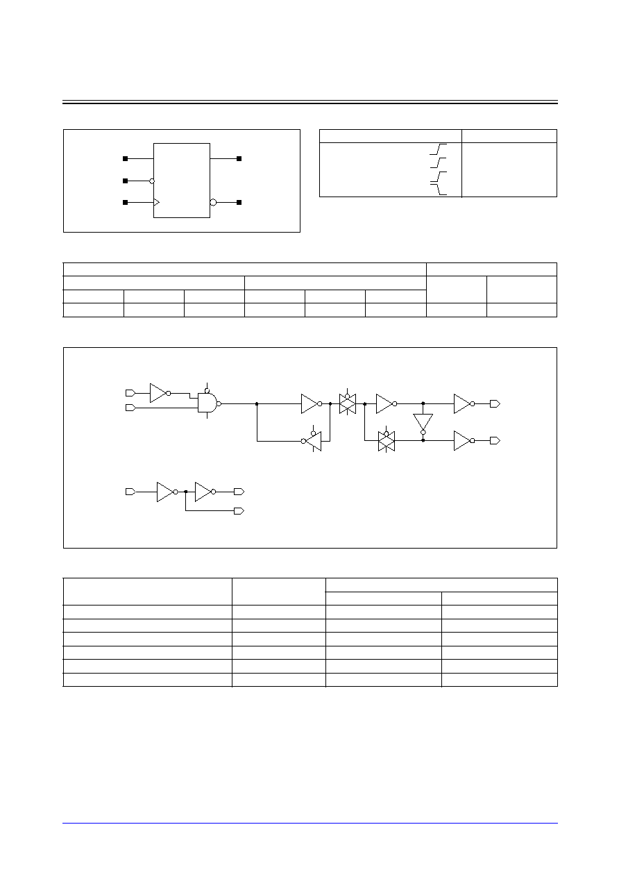
STDL131
3-280
Samsung ASIC
FDS3_LP/FDS3D2_LP
D Flip-Flop with Synchronous Set, 1X/2X Drive
Logic Symbol
Cell Data
Schematic Diagram
Timing Requirements
(Typical process, 25
∞
C, 1.8V, Unit = ns)
Input Load (SL)
Gate Count
FDS3_LP
FDS3D2_LP
FDS3_LP
FDS3D2_LP
D
CSN
CK
D
CSN
CK
0.9
0.7
1.1
0.9
0.7
1.1
6.33
7.00
Parameter
Symbol
Value (ns)
FDS3_LP
FDS3D2_LP
Input Setup Time (D to CK)
t
SU
0.297
0.297
Input Hold Time (D to CK)
t
HD
0.010
0.010
Input Setup Time (CSN to CK)
t
SU
0.222
0.222
Input Hold Time (CSN to CK)
t
HD
0.010
0.010
Pulse Width Low (CK)
t
PWL
0.262
0.262
Pulse Width High (CK)
t
PWH
0.154
0.168
D
CSN
CK
Q
QN
CL
CLB
Q
CLB
CL
CLB
CL
QN
D
CK
CL
CLB
CSN
CL
CLB
Truth Table
D
CSN
CK
Q (n+1) QN (n+1)
0
1
0
1
1
1
1
0
x
0
1
0
x
x
Q (n)
QN (n)
Samsung ASIC
3-281
STDL131
FDS3_LP/FDS3D2_LP
D Flip-Flop with Synchronous Set, 1X/2X Drive
Switching Characteristics
(Typical process, 25
∞
C, 1.8V, t
R
/t
F
= 0.19ns, SL: Standard Load)
FDS3_LP
FDS3D2_LP
Path
Parameter
Delay [ns]
SL = 2
Delay Equations [ns]
Group1*
Group2*
Group3*
CK to Q
tR
0.090
0.040 + 0.025*SL
0.035 + 0.027*SL
0.033 + 0.027*SL
tF
0.069
0.036 + 0.017*SL
0.036 + 0.017*SL
0.029 + 0.017*SL
tPLH
0.350
0.324 + 0.013*SL
0.326 + 0.013*SL
0.327 + 0.013*SL
tPHL
0.351
0.328 + 0.011*SL
0.333 + 0.010*SL
0.336 + 0.010*SL
CK to QN
tR
0.094
0.043 + 0.025*SL
0.039 + 0.026*SL
0.037 + 0.027*SL
tF
0.071
0.037 + 0.017*SL
0.038 + 0.017*SL
0.035 + 0.017*SL
tPLH
0.296
0.270 + 0.013*SL
0.272 + 0.013*SL
0.274 + 0.013*SL
tPHL
0.292
0.269 + 0.012*SL
0.275 + 0.010*SL
0.279 + 0.010*SL
*Group1 : SL < 4, *Group2 : 4 SL
<
<
=
= 8, *Group3 : 8 < SL
Path
Parameter
Delay [ns]
SL = 2
Delay Equations [ns]
Group1*
Group2*
Group3*
CK to Q
tR
0.064
0.039 + 0.012*SL
0.037 + 0.013*SL
0.031 + 0.013*SL
tF
0.053
0.037 + 0.008*SL
0.036 + 0.008*SL
0.032 + 0.009*SL
tPLH
0.376
0.361 + 0.007*SL
0.365 + 0.006*SL
0.367 + 0.006*SL
tPHL
0.374
0.360 + 0.007*SL
0.366 + 0.005*SL
0.373 + 0.005*SL
CK to QN
tR
0.069
0.046 + 0.012*SL
0.043 + 0.013*SL
0.036 + 0.013*SL
tF
0.058
0.040 + 0.009*SL
0.041 + 0.009*SL
0.042 + 0.009*SL
tPLH
0.300
0.284 + 0.008*SL
0.289 + 0.007*SL
0.293 + 0.006*SL
tPHL
0.299
0.283 + 0.008*SL
0.291 + 0.006*SL
0.300 + 0.005*SL
*Group1 : SL < 4, *Group2 : 4 SL
<
<
=
= 12, *Group3 : 12 < SL
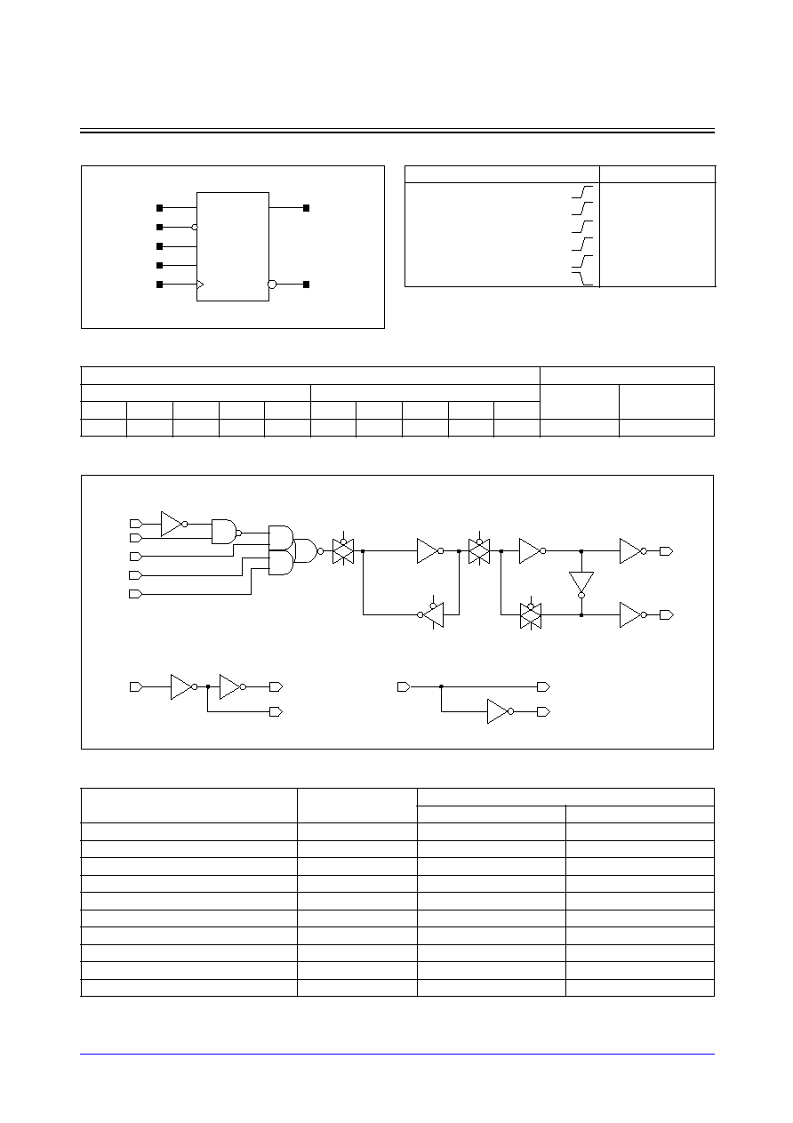
STDL131
3-282
Samsung ASIC
FDS3S_LP/FDS3SD2_LP
Flip-Flop with Synchronous Set, Scan, 1X/2X Drive
Logic Symbol
Cell Data
Schematic Diagram
Timing Requirements
(Typical process, 25
∞
C, 1.8V, Unit = ns)
Input Load (SL)
Gate Count
FDS3S_LP
FDS3SD2_LP
FDS3S_LP FDS3SD2_LP
D
CSN
CK
TI
TE
D
CSN
CK
TI
TE
0.9
0.7
1.1
0.7
1.6
0.9
0.7
1.1
0.7
1.6
8.33
8.67
Parameter
Symbol
Value (ns)
FDS3S_LP
FDS3SD2_LP
Input Setup Time (D to CK)
t
SU
0.434
0.431
Input Hold Time (D to CK)
t
HD
0.010
0.010
Input Setup Time (CSN to CK)
t
SU
0.365
0.361
Input Hold Time (CSN to CK)
t
HD
0.010
0.010
Pulse Width Low (CK)
t
PWL
0.307
0.310
Pulse Width High (CK)
t
PWH
0.155
0.170
Input Setup Time (TI to CK)
t
SU
0.328
0.326
Input Hold Time (TI to CK)
t
HD
0.010
0.010
Input Setup Time (TE to CK)
t
SU
0.313
0.313
Input Hold Time (TE to CK)
t
HD
0.010
0.010
Q
QN
D
TE
CK
CSN
TI
CLB
CL
CLB
CL
QN
Q
D
CSN
TI
CK
CL
CLB
TE
TE
TEB
CLB
CL
TEB
TE
CLB
CL
Truth Table
D
CSN
TI
TE
CK
Q(n+1) QN(n+1)
0
1
x
0
0
1
1
1
x
0
1
0
x
x
0
1
0
1
x
x
1
1
1
0
x
0
x
0
1
0
x
x
x
x
Q(n)
QN(n+1)

Samsung ASIC
3-283
STDL131
FDS3S_LP/FDS3SD2_LP
Flip-Flop with Synchronous Set, Scan, 1X/2X Drive
Switching Characteristics
(Typical process, 25
∞
C, 1.8V, t
R
/t
F
= 0.19ns, SL: Standard Load)
FDS3S_LP
FDS3SD2_LP
Path
Parameter
Delay [ns]
SL = 2
Delay Equations [ns]
Group1*
Group2*
Group3*
CK to Q
tR
0.095
0.044 + 0.025*SL
0.040 + 0.026*SL
0.037 + 0.027*SL
tF
0.071
0.037 + 0.017*SL
0.038 + 0.017*SL
0.034 + 0.017*SL
tPLH
0.299
0.273 + 0.013*SL
0.275 + 0.013*SL
0.277 + 0.013*SL
tPHL
0.296
0.272 + 0.012*SL
0.278 + 0.010*SL
0.283 + 0.010*SL
CK to QN
tR
0.092
0.042 + 0.025*SL
0.037 + 0.026*SL
0.034 + 0.027*SL
tF
0.070
0.037 + 0.016*SL
0.035 + 0.017*SL
0.032 + 0.017*SL
tPLH
0.354
0.328 + 0.013*SL
0.330 + 0.013*SL
0.331 + 0.013*SL
tPHL
0.354
0.332 + 0.011*SL
0.337 + 0.010*SL
0.339 + 0.010*SL
*Group1 : SL < 4, *Group2 : 4 SL
<
<
=
= 8, *Group3 : 8 < SL
Path
Parameter
Delay [ns]
SL = 2
Delay Equations [ns]
Group1*
Group2*
Group3*
CK to Q
tR
0.070
0.046 + 0.012*SL
0.043 + 0.013*SL
0.037 + 0.013*SL
tF
0.058
0.042 + 0.008*SL
0.040 + 0.009*SL
0.042 + 0.008*SL
tPLH
0.305
0.289 + 0.008*SL
0.294 + 0.007*SL
0.298 + 0.006*SL
tPHL
0.307
0.291 + 0.008*SL
0.299 + 0.006*SL
0.308 + 0.005*SL
CK to QN
tR
0.064
0.040 + 0.012*SL
0.037 + 0.013*SL
0.031 + 0.013*SL
tF
0.053
0.034 + 0.009*SL
0.039 + 0.008*SL
0.034 + 0.009*SL
tPLH
0.384
0.369 + 0.007*SL
0.373 + 0.006*SL
0.375 + 0.006*SL
tPHL
0.379
0.365 + 0.007*SL
0.371 + 0.005*SL
0.378 + 0.005*SL
*Group1 : SL < 4, *Group2 : 4 SL
<
<
=
= 12, *Group3 : 12 < SL
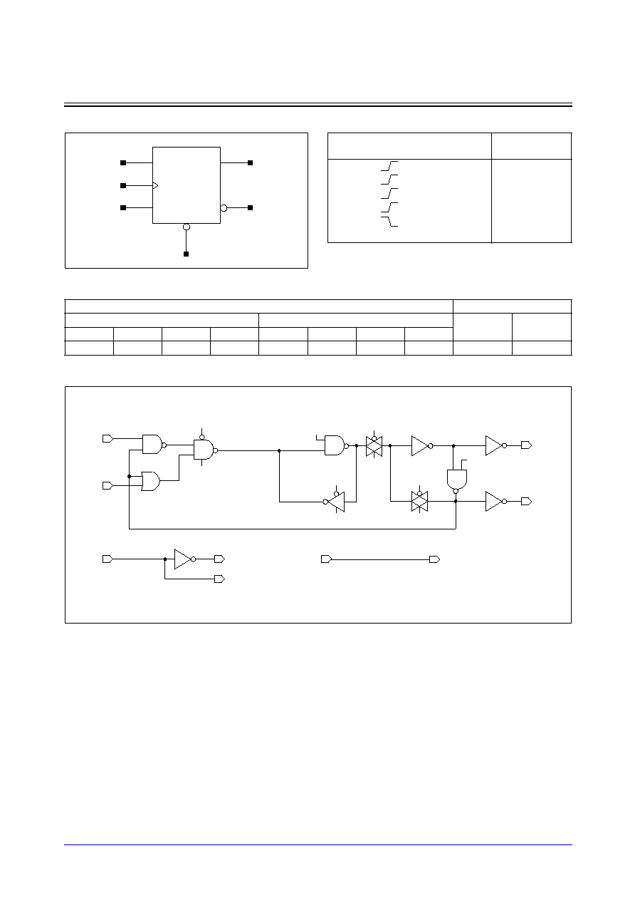
STDL131
3-284
Samsung ASIC
FJ2_LP/FJ2D2_LP
JK Flip-Flop with Reset, 1X/2X Drive
Logic Symbol
Cell Data
Schematic Diagram
Input Load (SL)
Gate Count
FJ2_LP
FJ2D2_LP
FJ2_LP
FJ2D2_LP
J
K
CK
RN
J
K
CK
RN
0.7
0.7
1.1
2.0
0.7
0.7
1.1
2.1
8.67
9.00
J
CK
K
Q
QN
RN
CL
CLB
CLB
CL
Q
QN
J
K
CK
CL
CLB
RN
RN
RN
CL
CLB
CL
CLB
RN
Truth Table
J
CK
K
RN
Q
(n+1)
QN
(n+1)
0
1
1
0
1
1
0
1
1
0
0
0
1
Q (n)
QN (n)
1
1
1
QN (n)
Q (n)
x
x
1
Q (n)
QN (n)
x
x
x
0
0
1
Samsung ASIC
3-285
STDL131
FJ2_LP/FJ2D2_LP
JK Flip-Flop with Reset, 1X/2X Drive
Timing Requirements
(Typical process, 25
∞
C, 1.8V, Unit = ns)
Switching Characteristics
(Typical process, 25
∞
C, 1.8V, t
R
/t
F
= 0.19ns, SL: Standard Load)
FJ2_LP
FJ2D2_LP
Parameter
Symbol
Value (ns)
FJ2_LP
FJ2D2_LP
Input Setup Time (J to CK)
t
SU
0.292
0.292
Input Hold Time (J to CK)
t
HD
0.010
0.010
Input Setup Time (K to CK)
t
SU
0.292
0.292
Input Hold Time (K to CK)
t
HD
0.010
0.010
Pulse Width Low (CK)
t
PWL
0.320
0.320
Pulse Width High (CK)
t
PWH
0.168
0.184
Pulse Width Low (RN)
t
PWL
0.371
0.409
Recovery Time (RN to CK)
t
RC
0.010
0.010
Removal Time (RN to CK)
t
RM
0.165
0.165
Path
Parameter
Delay [ns]
SL = 2
Delay Equations [ns]
Group1*
Group2*
Group3*
CK to Q
tR
0.116
0.067 + 0.025*SL
0.066 + 0.025*SL
0.062 + 0.025*SL
tF
0.083
0.049 + 0.017*SL
0.054 + 0.016*SL
0.050 + 0.016*SL
tPLH
0.456
0.424 + 0.016*SL
0.434 + 0.014*SL
0.440 + 0.013*SL
tPHL
0.405
0.379 + 0.013*SL
0.388 + 0.011*SL
0.395 + 0.010*SL
RN to Q
tF
0.093
0.058 + 0.018*SL
0.059 + 0.017*SL
0.061 + 0.017*SL
tPHL
0.233
0.204 + 0.014*SL
0.215 + 0.012*SL
0.224 + 0.011*SL
CK to QN
tR
0.095
0.044 + 0.025*SL
0.042 + 0.026*SL
0.037 + 0.026*SL
tF
0.072
0.038 + 0.017*SL
0.040 + 0.016*SL
0.035 + 0.017*SL
tPLH
0.302
0.276 + 0.013*SL
0.279 + 0.013*SL
0.280 + 0.013*SL
tPHL
0.315
0.292 + 0.012*SL
0.298 + 0.010*SL
0.302 + 0.010*SL
RN to QN
tR
0.110
0.064 + 0.023*SL
0.056 + 0.025*SL
0.048 + 0.026*SL
tPLH
0.511
0.482 + 0.014*SL
0.489 + 0.013*SL
0.491 + 0.012*SL
*Group1 : SL < 4, *Group2 : 4 SL
<
<
=
= 8, *Group3 : 8 < SL
Path
Parameter
Delay [ns]
SL = 2
Delay Equations [ns]
Group1*
Group2*
Group3*
CK to Q
tR
0.084
0.058 + 0.013*SL
0.060 + 0.013*SL
0.057 + 0.013*SL
tF
0.063
0.042 + 0.010*SL
0.051 + 0.008*SL
0.050 + 0.008*SL
tPLH
0.467
0.447 + 0.010*SL
0.457 + 0.007*SL
0.468 + 0.007*SL
tPHL
0.423
0.406 + 0.009*SL
0.415 + 0.006*SL
0.429 + 0.005*SL
RN to Q
tF
0.072
0.052 + 0.010*SL
0.058 + 0.009*SL
0.060 + 0.009*SL
tPHL
0.222
0.203 + 0.010*SL
0.214 + 0.007*SL
0.229 + 0.006*SL
CK to QN
tR
0.070
0.048 + 0.011*SL
0.042 + 0.013*SL
0.035 + 0.013*SL
tF
0.059
0.040 + 0.009*SL
0.045 + 0.008*SL
0.040 + 0.009*SL
tPLH
0.306
0.290 + 0.008*SL
0.296 + 0.007*SL
0.299 + 0.006*SL
tPHL
0.322
0.307 + 0.008*SL
0.315 + 0.006*SL
0.324 + 0.005*SL
RN to QN
tR
0.088
0.065 + 0.012*SL
0.064 + 0.012*SL
0.050 + 0.013*SL
tPLH
0.539
0.520 + 0.010*SL
0.530 + 0.007*SL
0.538 + 0.006*SL
*Group1 : SL < 4, *Group2 : 4 SL
<
<
=
= 12, *Group3 : 12 < SL
STDL131
3-286
Samsung ASIC
FJ2S_LP/FJ2SD2_LP
JK Flip-Flop with Reset, Scan, 1X/2X Drive
Logic Symbol
Cell Data
Schematic Diagram
Timing Requirements
(Typical process, 25
∞
C, 1.8V, Unit = ns)
Input Load (SL)
Gate Count
FJ2S_LP
FJ2SD2_LP
FJ2S_LP
FJ2SD2_LP
J
K
CK
RN
TI
TE
J
K
CK
RN
TI
TE
0.7
0.9
1.1
1.5
0.7
1.6
0.7
0.9
1.1
1.6
0.7
1.6
10.33
11.00
Parameter
Symbol
Value (ns)
FJ2S_LP
FJ2SD2_LP
Input Setup Time (J to CK)
t
SU
0.490
0.491
Input Hold Time (J to CK)
t
HD
0.010
0.010
Input Setup Time (K to CK)
t
SU
0.490
0.491
Input Hold Time (K to CK)
t
HD
0.010
0.010
Pulse Width Low (CK)
t
PWL
0.310
0.310
Pulse Width High (CK)
t
PWH
0.182
0.202
Pulse Width Low (RN)
t
PWL
0.221
0.273
Recovery Time (RN to CK)
t
RC
0.010
0.010
Removal Time (RN to CK)
t
RM
0.902
0.904
Input Setup Time (TI to CK)
t
SU
0.334
0.334
Input Hold Time (TI to CK)
t
HD
0.010
0.010
Input Setup Time (TE to CK)
t
SU
0.327
0.327
Input Hold Time (TE to CK)
t
HD
0.010
0.010
Q
QN
J
TI
TE
CK
K
RN
CL
CLB
CLB
CL
CLB
CL
TE
TEB
Q
QN
J
K
TI
CK
CL
CLB
RN
RN
RN
TEB
TE
TE
CL
CLB
RN
Truth Table
J
CK
K
TI
TE
RN
Q
(n+1)
QN
(n+1)
0
1
x
0
1
0
1
1
0
x
0
1
1
0
0
0
x
0
1
Q (n) QN (n)
1
1
x
0
1
QN (n) Q (n)
x
x
x
x
1
Q (n) QN (n)
x
x
x
x
x
0
0
1
x
x
0
1
1
0
1
x
x
1
1
1
1
0

Samsung ASIC
3-287
STDL131
FJ2S_LP/FJ2SD2_LP
JK Flip-Flop with Reset, Scan, 1X/2X Drive
Switching Characteristics
(Typical process, 25
∞
C, 1.8V, t
R
/t
F
= 0.19ns, SL: Standard Load)
FJ2S_LP
FJ2SD2_LP
Path
Parameter
Delay [ns]
SL = 2
Delay Equations [ns]
Group1*
Group2*
Group3*
CK to Q
tR
0.115
0.065 + 0.025*SL
0.064 + 0.026*SL
0.060 + 0.026*SL
tF
0.082
0.047 + 0.018*SL
0.051 + 0.017*SL
0.049 + 0.017*SL
tPLH
0.367
0.334 + 0.016*SL
0.344 + 0.014*SL
0.352 + 0.013*SL
tPHL
0.337
0.310 + 0.014*SL
0.320 + 0.011*SL
0.329 + 0.010*SL
RN to Q
tF
0.086
0.051 + 0.018*SL
0.055 + 0.017*SL
0.054 + 0.017*SL
tPHL
0.213
0.184 + 0.014*SL
0.195 + 0.011*SL
0.204 + 0.010*SL
CK to QN
tR
0.094
0.043 + 0.026*SL
0.041 + 0.026*SL
0.036 + 0.027*SL
tF
0.072
0.040 + 0.016*SL
0.038 + 0.017*SL
0.034 + 0.017*SL
tPLH
0.399
0.373 + 0.013*SL
0.375 + 0.013*SL
0.376 + 0.013*SL
tPHL
0.426
0.403 + 0.011*SL
0.409 + 0.010*SL
0.412 + 0.010*SL
RN to QN
tR
0.107
0.052 + 0.027*SL
0.054 + 0.027*SL
0.058 + 0.026*SL
tPLH
0.293
0.262 + 0.015*SL
0.266 + 0.014*SL
0.274 + 0.013*SL
*Group1 : SL < 4, *Group2 : 4 SL
<
<
=
= 8, *Group3 : 8 < SL
Path
Parameter
Delay [ns]
SL = 2
Delay Equations [ns]
Group1*
Group2*
Group3*
CK to Q
tR
0.090
0.063 + 0.013*SL
0.065 + 0.013*SL
0.064 + 0.013*SL
tF
0.068
0.048 + 0.010*SL
0.052 + 0.009*SL
0.059 + 0.008*SL
tPLH
0.367
0.345 + 0.011*SL
0.356 + 0.008*SL
0.370 + 0.007*SL
tPHL
0.342
0.324 + 0.009*SL
0.334 + 0.007*SL
0.350 + 0.005*SL
RN to Q
tF
0.072
0.053 + 0.009*SL
0.056 + 0.009*SL
0.062 + 0.008*SL
tPHL
0.218
0.199 + 0.010*SL
0.210 + 0.007*SL
0.226 + 0.005*SL
CK to QN
tR
0.067
0.044 + 0.012*SL
0.039 + 0.013*SL
0.032 + 0.013*SL
tF
0.055
0.039 + 0.008*SL
0.038 + 0.008*SL
0.035 + 0.009*SL
tPLH
0.427
0.412 + 0.008*SL
0.417 + 0.006*SL
0.419 + 0.006*SL
tPHL
0.453
0.438 + 0.007*SL
0.445 + 0.006*SL
0.452 + 0.005*SL
RN to QN
tR
0.073
0.046 + 0.013*SL
0.046 + 0.013*SL
0.049 + 0.013*SL
tPLH
0.318
0.300 + 0.009*SL
0.306 + 0.007*SL
0.312 + 0.007*SL
*Group1 : SL < 4, *Group2 : 4 SL
<
<
=
= 12, *Group3 : 12 < SL
STDL131
3-288
Samsung ASIC
FJ4_LP/FJ4D2_LP
JK Flip-Flop with Reset, Set, 1X/2X Drive
Logic Symbol5
Cell Data
Schematic Diagram
Input Load (SL)
Gate Count
FJ4_LP
FJ4D2_LP
FJ4_LP
FJ4D2_LP
J
K
CK
RN
SN
J
K
CK
RN
SN
0.7
0.7
1.1
2.0
1.5
0.7
0.7
1.1
2.2
1.5
9.67
10.00
J
CK
K
Q
QN
RN
SN
J
CL
CLB
K
Q
QN
CL
CLB
CLB
CL
CLB
CL
RN
SN
CL
CK
CLB
Truth Table
J
CK
K
RN
SN
Q
(n+1)
QN
(n+1)
0
1
1
1
0
1
1
0
1
1
1
0
0
0
1
1
Q (n) QN (n)
1
1
1
1
QN (n) Q (n)
x
x
1
1
Q (n) QN (n)
x
x
x
0
1
0
1
x
x
x
1
0
1
0
x
x
x
0
0
0
0
Samsung ASIC
3-289
STDL131
FJ4_LP/FJ4D2_LP
JK Flip-Flop with Reset, Set, 1X/2X Drive
Timing Requirements
(Typical process, 25
∞
C, 1.8V, Unit = ns)
Switching Characteristics
(Typical process, 25
∞
C, 1.8V, t
R
/t
F
= 0.19ns, SL: Standard Load)
FJ4_LP
Parameter
Symbol
Value (ns)
FJ4_LP
FJ4D2_LP
Input Setup Time (J to CK)
t
SU
0.294
0.291
Input Hold Time (J to CK)
t
HD
0.010
0.010
Input Setup Time (K to CK)
t
SU
0.294
0.291
Input Hold Time (K to CK)
t
HD
0.010
0.010
Pulse Width Low (CK)
t
PWL
0.328
0.326
Pulse Width High (CK)
t
PWH
0.183
0.207
Pulse Width Low (RN)
t
PWL
0.386
0.425
Pulse Width Low (SN)
t
PWL
0.277
0.304
Recovery Time (RN to CK)
t
RC
0.010
0.010
Removal Time (RN to CK)
t
RM
0.223
0.222
Recovery Time (SN to CK)
t
RC
0.010
0.010
Removal Time (SN to CK)
t
RM
0.964
0.959
Recovery Time (SN to RN)
t
RC
0.071
0.069
Removal Time (SN to RN)
t
RM
0.010
0.010
Path
Parameter
Delay [ns]
SL = 2
Delay Equations [ns]
Group1*
Group2*
Group3*
CK to Q
tR
0.118
0.068 + 0.025*SL
0.068 + 0.025*SL
0.063 + 0.025*SL
tF
0.084
0.051 + 0.017*SL
0.051 + 0.016*SL
0.052 + 0.016*SL
tPLH
0.478
0.446 + 0.016*SL
0.455 + 0.014*SL
0.462 + 0.013*SL
tPHL
0.450
0.423 + 0.013*SL
0.432 + 0.011*SL
0.440 + 0.010*SL
RN to Q
tR
0.131
0.074 + 0.028*SL
0.082 + 0.026*SL
0.090 + 0.025*SL
tF
0.093
0.057 + 0.018*SL
0.063 + 0.017*SL
0.059 + 0.017*SL
tPLH
0.226
0.189 + 0.018*SL
0.199 + 0.016*SL
0.213 + 0.014*SL
tPHL
0.233
0.204 + 0.014*SL
0.214 + 0.012*SL
0.224 + 0.011*SL
SN to Q
tR
0.133
0.076 + 0.028*SL
0.083 + 0.027*SL
0.091 + 0.025*SL
tPLH
0.354
0.317 + 0.018*SL
0.327 + 0.016*SL
0.341 + 0.014*SL
CK to QN
tR
0.106
0.057 + 0.025*SL
0.054 + 0.025*SL
0.051 + 0.026*SL
tF
0.077
0.044 + 0.017*SL
0.047 + 0.016*SL
0.041 + 0.017*SL
tPLH
0.342
0.312 + 0.015*SL
0.319 + 0.013*SL
0.322 + 0.013*SL
tPHL
0.334
0.309 + 0.012*SL
0.317 + 0.010*SL
0.323 + 0.010*SL
RN to QN
tR
0.119
0.072 + 0.023*SL
0.068 + 0.024*SL
0.060 + 0.025*SL
tPLH
0.548
0.517 + 0.016*SL
0.527 + 0.013*SL
0.532 + 0.013*SL
SN to QN
tR
0.106
0.057 + 0.025*SL
0.055 + 0.025*SL
0.048 + 0.026*SL
tF
0.079
0.046 + 0.016*SL
0.045 + 0.016*SL
0.041 + 0.017*SL
tPLH
0.177
0.147 + 0.015*SL
0.154 + 0.013*SL
0.158 + 0.012*SL
tPHL
0.187
0.162 + 0.012*SL
0.170 + 0.010*SL
0.175 + 0.010*SL
*Group1 : SL < 4, *Group2 : 4 SL
<
<
=
= 8, *Group3 : 8 < SL

STDL131
3-290
Samsung ASIC
FJ4_LP/FJ4D2_LP
JK Flip-Flop with Reset, Set, 1X/2X Drive
Switching Characteristics
(Typical process, 25
∞
C, 1.8V, t
R
/t
F
= 0.19ns, SL: Standard Load)
FJ4D2_LP
Path
Parameter
Delay [ns]
SL = 2
Delay Equations [ns]
Group1*
Group2*
Group3*
CK to Q
tR
0.085
0.059 + 0.013*SL
0.062 + 0.012*SL
0.056 + 0.013*SL
tF
0.065
0.044 + 0.010*SL
0.053 + 0.008*SL
0.051 + 0.008*SL
tPLH
0.491
0.471 + 0.010*SL
0.481 + 0.008*SL
0.493 + 0.007*SL
tPHL
0.478
0.460 + 0.009*SL
0.470 + 0.006*SL
0.484 + 0.005*SL
RN to Q
tR
0.090
0.059 + 0.015*SL
0.066 + 0.014*SL
0.074 + 0.013*SL
tF
0.071
0.049 + 0.011*SL
0.058 + 0.009*SL
0.059 + 0.009*SL
tPLH
0.200
0.178 + 0.011*SL
0.188 + 0.008*SL
0.203 + 0.007*SL
tPHL
0.221
0.202 + 0.009*SL
0.212 + 0.007*SL
0.227 + 0.006*SL
SN to Q
tR
0.093
0.062 + 0.015*SL
0.068 + 0.014*SL
0.077 + 0.013*SL
tPLH
0.357
0.335 + 0.011*SL
0.345 + 0.009*SL
0.361 + 0.007*SL
CK to QN
tR
0.083
0.056 + 0.013*SL
0.059 + 0.012*SL
0.053 + 0.013*SL
tF
0.065
0.046 + 0.009*SL
0.051 + 0.008*SL
0.048 + 0.008*SL
tPLH
0.348
0.329 + 0.010*SL
0.338 + 0.007*SL
0.349 + 0.006*SL
tPHL
0.341
0.324 + 0.008*SL
0.333 + 0.006*SL
0.345 + 0.005*SL
RN to QN
tR
0.095
0.068 + 0.014*SL
0.075 + 0.012*SL
0.066 + 0.013*SL
tPLH
0.576
0.555 + 0.011*SL
0.567 + 0.008*SL
0.581 + 0.006*SL
SN to QN
tR
0.081
0.054 + 0.014*SL
0.060 + 0.012*SL
0.052 + 0.013*SL
tF
0.063
0.043 + 0.010*SL
0.050 + 0.008*SL
0.047 + 0.008*SL
tPLH
0.183
0.163 + 0.010*SL
0.173 + 0.007*SL
0.183 + 0.006*SL
tPHL
0.191
0.175 + 0.008*SL
0.184 + 0.006*SL
0.195 + 0.005*SL
*Group1 : SL < 4, *Group2 : 4 SL
<
<
=
= 12, *Group3 : 12 < SL
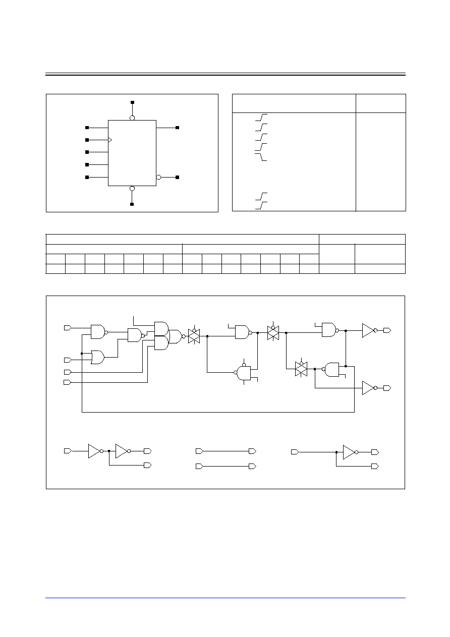
Samsung ASIC
3-291
STDL131
FJ4S_LP/FJ4SD2_LP
JK Flip-Flop with Reset, Set, Scan, 1X/2X Drive
Logic Symbol
Cell Data
Schematic Diagram
Input Load (SL)
Gate Count
FJ4S_LP
FJ4SD2_LP
FJ4S_LP
FJ4SD2_LP
J
K
CK
RN
SN
TI
TE
J
K
CK
RN
SN
TI
TE
0.7
0.9
1.2
1.5
2.1
0.7
1.6
0.7
0.9
1.2
1.5
2.2
0.7
1.6
13.33
14.00
Q
QN
J
TI
TE
CK
K
RN
SN
CL
CLB
CLB
CL
CLB
CL
Q
QN
J
K
TI
CL
CLB
CK
CL
CLB
RN
RN
RN
SN
RN
SN
SN
SN
TE
TE
TEB
TE
TEB
Truth Table
J
CK
K
TI
TE
RN SN
Q
(n+1)
QN
(n+1)
0
1
x
0
1
1
0
1
1
0
x
0
1
1
1
0
0
0
x
0
1
1
Q (n) QN (n)
1
1
x
0
1
1
QN (n) Q (n)
x
x
x
x
1
1
Q (n) QN (n)
x
x
x
x
x
0
1
0
1
x
x
x
x
x
1
0
1
0
x
x
x
x
x
0
0
0
0
x
x
0
1
1
1
0
1
x
x
1
1
1
1
1
0
STDL131
3-292
Samsung ASIC
FJ4S_LP/FJ4SD2_LP
JK Flip-Flop with Reset, Set, Scan, 1X/2X Drive
Timing Requirements
(Typical process, 25
∞
C, 1.8V, Unit = ns)
Switching Characteristics
(Typical process, 25
∞
C, 1.8V, t
R
/t
F
= 0.19ns, SL: Standard Load)
FJ4S_LP
Parameter
Symbol
Value (ns)
FJ4S_LP
FJ4SD2_LP
Input Setup Time (J to CK)
t
SU
0.497
0.497
Input Hold Time (J to CK)
t
HD
0.010
0.010
Input Setup Time (K to CK)
t
SU
0.497
0.497
Input Hold Time (K to CK)
t
HD
0.010
0.010
Pulse Width Low (CK)
t
PWL
0.335
0.336
Pulse Width High (CK)
t
PWH
0.195
0.220
Pulse Width Low (RN)
t
PWL
0.276
0.316
Pulse Width Low (SN)
t
PWL
0.400
0.439
Recovery Time (RN to CK)
t
RC
0.010
0.010
Removal Time (RN to CK)
t
RM
0.939
0.942
Recovery Time (SN to CK)
t
RC
0.010
0.010
Removal Time (SN to CK)
t
RM
0.209
0.211
Input Setup Time (TI to CK)
t
SU
0.383
0.383
Input Hold Time (TI to CK)
t
HD
0.010
0.010
Input Setup Time (TE to CK)
t
SU
0.363
0.364
Input Hold Time (TE to CK)
t
HD
0.010
0.010
Recovery Time (SN to RN)
t
RC
0.010
0.010
Removal Time (SN to RN)
t
RM
0.058
0.058
Path
Parameter
Delay [ns]
SL = 2
Delay Equations [ns]
Group1*
Group2*
Group3*
CK to Q
tR
0.119
0.068 + 0.025*SL
0.070 + 0.025*SL
0.065 + 0.026*SL
tF
0.086
0.051 + 0.017*SL
0.055 + 0.016*SL
0.056 + 0.016*SL
tPLH
0.377
0.344 + 0.017*SL
0.355 + 0.014*SL
0.363 + 0.013*SL
tPHL
0.362
0.334 + 0.014*SL
0.345 + 0.011*SL
0.354 + 0.010*SL
RN to Q
tR
0.116
0.067 + 0.025*SL
0.066 + 0.025*SL
0.059 + 0.026*SL
tF
0.087
0.054 + 0.017*SL
0.055 + 0.017*SL
0.055 + 0.016*SL
tPLH
0.210
0.178 + 0.016*SL
0.188 + 0.014*SL
0.195 + 0.013*SL
tPHL
0.219
0.191 + 0.014*SL
0.202 + 0.011*SL
0.212 + 0.010*SL
SN to Q
tR
0.128
0.080 + 0.024*SL
0.078 + 0.024*SL
0.070 + 0.025*SL
tPLH
0.560
0.526 + 0.017*SL
0.539 + 0.014*SL
0.548 + 0.013*SL
CK to QN
tR
0.105
0.057 + 0.024*SL
0.053 + 0.025*SL
0.046 + 0.026*SL
tF
0.075
0.042 + 0.016*SL
0.043 + 0.016*SL
0.039 + 0.017*SL
tPLH
0.465
0.437 + 0.014*SL
0.443 + 0.013*SL
0.445 + 0.012*SL
tPHL
0.453
0.429 + 0.012*SL
0.436 + 0.010*SL
0.441 + 0.010*SL
RN to QN
tR
0.123
0.065 + 0.029*SL
0.073 + 0.027*SL
0.082 + 0.026*SL
tPLH
0.349
0.314 + 0.018*SL
0.321 + 0.016*SL
0.333 + 0.014*SL
SN to QN
tR
0.120
0.063 + 0.029*SL
0.069 + 0.027*SL
0.078 + 0.026*SL
tF
0.080
0.045 + 0.018*SL
0.048 + 0.017*SL
0.043 + 0.018*SL
tPLH
0.186
0.151 + 0.017*SL
0.158 + 0.016*SL
0.170 + 0.014*SL
tPHL
0.196
0.170 + 0.013*SL
0.178 + 0.011*SL
0.183 + 0.010*SL
*Group1 : SL < 4, *Group2 : 4 SL
<
<
=
= 8, *Group3 : 8 < SL
Samsung ASIC
3-293
STDL131
FJ4S_LP/FJ4SD2_LP
JK Flip-Flop with Reset, Set, Scan, 1X/2X Drive
Switching Characteristics
(Typical process, 25
∞
C, 1.8V, t
R
/t
F
= 0.19ns, SL: Standard Load)
FJ4SD2_LP
Path
Parameter
Delay [ns]
SL = 2
Delay Equations [ns]
Group1*
Group2*
Group3*
CK to Q
tR
0.094
0.068 + 0.013*SL
0.070 + 0.013*SL
0.070 + 0.013*SL
tF
0.072
0.052 + 0.010*SL
0.058 + 0.008*SL
0.061 + 0.008*SL
tPLH
0.379
0.357 + 0.011*SL
0.368 + 0.008*SL
0.383 + 0.007*SL
tPHL
0.366
0.348 + 0.009*SL
0.358 + 0.007*SL
0.374 + 0.005*SL
RN to Q
tR
0.092
0.065 + 0.013*SL
0.070 + 0.012*SL
0.066 + 0.013*SL
tF
0.073
0.052 + 0.010*SL
0.061 + 0.008*SL
0.062 + 0.008*SL
tPLH
0.211
0.190 + 0.010*SL
0.201 + 0.008*SL
0.215 + 0.006*SL
tPHL
0.221
0.202 + 0.009*SL
0.213 + 0.007*SL
0.230 + 0.005*SL
SN to Q
tR
0.104
0.077 + 0.013*SL
0.083 + 0.012*SL
0.078 + 0.012*SL
tPLH
0.588
0.566 + 0.011*SL
0.578 + 0.008*SL
0.596 + 0.007*SL
CK to QN
tR
0.079
0.054 + 0.013*SL
0.056 + 0.012*SL
0.049 + 0.013*SL
tF
0.061
0.043 + 0.009*SL
0.048 + 0.008*SL
0.044 + 0.008*SL
tPLH
0.489
0.471 + 0.009*SL
0.479 + 0.007*SL
0.487 + 0.006*SL
tPHL
0.488
0.473 + 0.008*SL
0.481 + 0.006*SL
0.491 + 0.005*SL
RN to QN
tR
0.088
0.058 + 0.015*SL
0.064 + 0.014*SL
0.072 + 0.013*SL
tPLH
0.364
0.344 + 0.010*SL
0.352 + 0.008*SL
0.364 + 0.007*SL
SN to QN
tR
0.085
0.056 + 0.015*SL
0.060 + 0.014*SL
0.069 + 0.013*SL
tF
0.064
0.045 + 0.010*SL
0.049 + 0.009*SL
0.048 + 0.009*SL
tPLH
0.172
0.153 + 0.010*SL
0.160 + 0.008*SL
0.171 + 0.007*SL
tPHL
0.195
0.179 + 0.008*SL
0.186 + 0.006*SL
0.197 + 0.005*SL
*Group1 : SL < 4, *Group2 : 4 SL
<
<
=
= 12, *Group3 : 12 < SL

STDL131
3-294
Samsung ASIC
FT2_LP/FT2D2_LP
Toggle Flip-Flop with Reset, 1X/2X Drive
Logic Symbol
Cell Data
Schematic Diagram
Timing Requirements
(Typical process, 25
∞
C, 1.8V, Unit = ns)
Input Load (SL)
Gate Count
FT2_LP
FT2D2_LP
FT2_LP
FT2D2_LP
CK
RN
CK
RN
1.1
2.0
1.1
2.1
6.67
6.67
Parameter
Symbol
Value (ns)
FT2_LP
FT2D2_LP
Pulse Width Low (CK)
t
PWL
0.167
0.163
Pulse Width High (CK)
t
PWH
0.132
0.149
Pulse Width Low (RN)
t
PWL
0.393
0.429
Recovery Time (RN to CK)
t
RC
0.010
0.010
Removal Time (RN to CK)
t
RM
0.158
0.159
CK
Q
QN
RN
CLB
CL
CLB
CL
Q
QN
CK
CL
CLB
RN
RN
RN
RN
CLB
CL
CLB
CL
Truth Table
CK
RN
Q (n+1)
QN (n+1)
1
QN (n)
Q (n)
1
Q (n)
QN (n)
x
0
0
1

Samsung ASIC
3-295
STDL131
FT2_LP/FT2D2_LP
Toggle Flip-Flop with Reset, 1X/2X Drive
Switching Characteristics
(Typical process, 25
∞
C, 1.8V, t
R
/t
F
= 0.19ns, SL: Standard Load)
FT2_LP
FT2D2_LP
Path
Parameter
Delay [ns]
SL = 2
Delay Equations [ns]
Group1*
Group2*
Group3*
CK to Q
tR
0.112
0.064 + 0.024*SL
0.060 + 0.025*SL
0.053 + 0.026*SL
tF
0.081
0.049 + 0.016*SL
0.048 + 0.016*SL
0.047 + 0.017*SL
tPLH
0.436
0.406 + 0.015*SL
0.414 + 0.013*SL
0.418 + 0.012*SL
tPHL
0.389
0.364 + 0.013*SL
0.372 + 0.010*SL
0.378 + 0.010*SL
RN to Q
tF
0.080
0.047 + 0.017*SL
0.047 + 0.017*SL
0.050 + 0.016*SL
tPHL
0.194
0.169 + 0.013*SL
0.176 + 0.011*SL
0.183 + 0.010*SL
CK to QN
tR
0.096
0.045 + 0.025*SL
0.042 + 0.026*SL
0.037 + 0.027*SL
tF
0.072
0.039 + 0.016*SL
0.037 + 0.017*SL
0.037 + 0.017*SL
tPLH
0.299
0.272 + 0.014*SL
0.275 + 0.013*SL
0.276 + 0.013*SL
tPHL
0.309
0.285 + 0.012*SL
0.292 + 0.010*SL
0.295 + 0.010*SL
RN to QN
tR
0.096
0.045 + 0.025*SL
0.042 + 0.026*SL
0.037 + 0.027*SL
tPLH
0.314
0.287 + 0.013*SL
0.291 + 0.013*SL
0.291 + 0.013*SL
*Group1 : SL < 4, *Group2 : 4 SL
<
<
=
= 8, *Group3 : 8 < SL
Path
Parameter
Delay [ns]
SL = 2
Delay Equations [ns]
Group1*
Group2*
Group3*
CK to Q
tR
0.079
0.053 + 0.013*SL
0.055 + 0.012*SL
0.048 + 0.013*SL
tF
0.060
0.040 + 0.010*SL
0.047 + 0.008*SL
0.045 + 0.008*SL
tPLH
0.444
0.425 + 0.009*SL
0.434 + 0.007*SL
0.443 + 0.006*SL
tPHL
0.408
0.392 + 0.008*SL
0.400 + 0.006*SL
0.412 + 0.005*SL
RN to Q
tF
0.061
0.042 + 0.009*SL
0.045 + 0.009*SL
0.049 + 0.008*SL
tPHL
0.186
0.170 + 0.008*SL
0.178 + 0.006*SL
0.189 + 0.005*SL
CK to QN
tR
0.070
0.047 + 0.011*SL
0.041 + 0.013*SL
0.036 + 0.013*SL
tF
0.059
0.041 + 0.009*SL
0.045 + 0.008*SL
0.041 + 0.008*SL
tPLH
0.304
0.287 + 0.008*SL
0.293 + 0.007*SL
0.297 + 0.006*SL
tPHL
0.317
0.301 + 0.008*SL
0.309 + 0.006*SL
0.318 + 0.005*SL
RN to QN
tR
0.071
0.047 + 0.012*SL
0.044 + 0.013*SL
0.036 + 0.013*SL
tPLH
0.318
0.302 + 0.008*SL
0.308 + 0.007*SL
0.312 + 0.006*SL
*Group1 : SL < 4, *Group2 : 4 SL
<
<
=
= 12, *Group3 : 12 < SL
STDL131
3-296
Samsung ASIC
LATCHES
Cell List
Cell Name
Function Description
LD1_LP
D Latch with Active High, 1X Drive
LD1D2_LP
D Latch with Active High, 2X Drive
LD1Q_LP
D Latch with Active High, Q Output Only, 1X Drive
LD1QD2_LP
D Latch with Active High, Q Output Only, 2X Drive
LD2_LP
D Latch with Active High, Reset, 1X Drive
LD2D2_LP
D Latch with Active High, Reset, 2X Drive
LD2Q_LP
D Latch with Active High, Reset, Q Output Only, 1X Drive
LD2QD2_LP
D Latch with Active High, Reset, Q Output Only, 2X Drive
LD3_LP
D Latch with Active High, Set, 1X Drive
LD3D2_LP
D Latch with Active High, Set, 2X Drive
LD4_LP
D Latch with Active High, Reset, Set, 1X Drive
LD4D2_LP
D Latch with Active High, Reset, Set, 2X Drive
LD5_LP
D Latch with Active Low, 1X Drive
LD5D2_LP
D Latch with Active Low, 2X Drive
LD5Q_LP
D Latch with Active Low, Q Output Only, 1X Drive
LD5QD2_LP
D Latch with Active Low, Q Output Only, 2X Drive
LD6_LP
D Latch with Active Low, Reset, 1X Drive
LD6D2_LP
D Latch with Active Low, Reset, 2X Drive
LD6Q_LP
D Latch with Active Low, Reset, Q Output Only, 1X Drive
LD6QD2_LP
D Latch with Active Low, Reset, Q Output Only, 2X Drive

Samsung ASIC
3-297
STDL131
LD1_LP/LD1D2_LP
D Latch with Active High, 1X/2X Drive
Logic Symbol
Cell Data
Schematic Diagram
Timing Requirements
(Typical process, 25
∞
C, 1.8V, Unit = ns)
Input Load (SL)
Gate Count
LD1_LP
LD1D2_LP
LD1_LP
LD1D2_LP
D
G
D
G
1.1
1.1
1.1
1.1
4.33
4.67
Parameter
Symbol
Value (ns)
LD1_LP
LD1D2_LP
Input Setup Time (D to G)
t
SU
0.142
0.200
Input Hold Time (D to G)
t
HD
0.010
0.010
Pulse Width High (G)
t
PWH
0.176
0.242
D
G
Q
QN
D
QN
Q
GL
GL
G
GB
GB
GL
GB
Truth Table
D
G
Q (n+1)
QN (n+1)
0
1
0
1
1
1
1
0
x
0
Q (n)
QN (n)
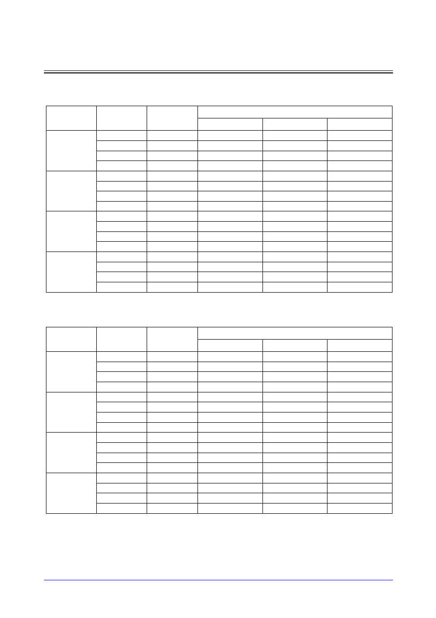
STDL131
3-298
Samsung ASIC
LD1_LP/LD1D2_LP
D Latch with Active High, 1X/2X Drive
Switching Characteristics
(Typical process, 25
∞
C, 1.8V, t
R
/t
F
= 0.19ns, SL: Standard Load)
LD1_LP
LD1D2_LP
Path
Parameter
Delay [ns]
SL = 2
Delay Equations [ns]
Group1*
Group2*
Group3*
D to Q
tR
0.107
0.056 + 0.025*SL
0.056 + 0.025*SL
0.051 + 0.026*SL
tF
0.097
0.060 + 0.019*SL
0.067 + 0.017*SL
0.069 + 0.017*SL
tPLH
0.198
0.168 + 0.015*SL
0.175 + 0.013*SL
0.180 + 0.013*SL
tPHL
0.230
0.200 + 0.015*SL
0.212 + 0.012*SL
0.225 + 0.010*SL
G to Q
tR
0.106
0.056 + 0.025*SL
0.056 + 0.025*SL
0.050 + 0.026*SL
tF
0.096
0.057 + 0.019*SL
0.066 + 0.017*SL
0.068 + 0.017*SL
tPLH
0.236
0.206 + 0.015*SL
0.212 + 0.013*SL
0.217 + 0.013*SL
tPHL
0.251
0.221 + 0.015*SL
0.233 + 0.012*SL
0.246 + 0.010*SL
D to QN
tR
0.096
0.046 + 0.025*SL
0.041 + 0.026*SL
0.038 + 0.027*SL
tF
0.071
0.038 + 0.017*SL
0.038 + 0.017*SL
0.033 + 0.017*SL
tPLH
0.298
0.271 + 0.013*SL
0.274 + 0.013*SL
0.275 + 0.013*SL
tPHL
0.258
0.235 + 0.011*SL
0.240 + 0.010*SL
0.243 + 0.010*SL
G to QN
tR
0.096
0.046 + 0.025*SL
0.041 + 0.026*SL
0.038 + 0.027*SL
tF
0.072
0.038 + 0.017*SL
0.039 + 0.017*SL
0.033 + 0.017*SL
tPLH
0.319
0.293 + 0.013*SL
0.295 + 0.013*SL
0.296 + 0.013*SL
tPHL
0.295
0.272 + 0.011*SL
0.278 + 0.010*SL
0.281 + 0.010*SL
*Group1 : SL < 4, *Group2 : 4 SL
<
<
=
= 8, *Group3 : 8 < SL
Path
Parameter
Delay [ns]
SL = 2
Delay Equations [ns]
Group1*
Group2*
Group3*
D to Q
tR
0.085
0.058 + 0.014*SL
0.061 + 0.013*SL
0.059 + 0.013*SL
tF
0.088
0.066 + 0.011*SL
0.072 + 0.009*SL
0.085 + 0.008*SL
tPLH
0.209
0.188 + 0.010*SL
0.198 + 0.008*SL
0.210 + 0.007*SL
tPHL
0.244
0.222 + 0.011*SL
0.236 + 0.008*SL
0.257 + 0.006*SL
G to Q
tR
0.085
0.059 + 0.013*SL
0.061 + 0.013*SL
0.059 + 0.013*SL
tF
0.087
0.065 + 0.011*SL
0.071 + 0.009*SL
0.084 + 0.008*SL
tPLH
0.241
0.221 + 0.010*SL
0.231 + 0.008*SL
0.243 + 0.007*SL
tPHL
0.265
0.243 + 0.011*SL
0.256 + 0.008*SL
0.278 + 0.006*SL
D to QN
tR
0.072
0.050 + 0.011*SL
0.044 + 0.012*SL
0.035 + 0.013*SL
tF
0.054
0.037 + 0.009*SL
0.039 + 0.008*SL
0.035 + 0.009*SL
tPLH
0.347
0.331 + 0.008*SL
0.337 + 0.007*SL
0.340 + 0.006*SL
tPHL
0.297
0.283 + 0.007*SL
0.289 + 0.006*SL
0.297 + 0.005*SL
G to QN
tR
0.071
0.049 + 0.011*SL
0.044 + 0.012*SL
0.035 + 0.013*SL
tF
0.055
0.037 + 0.009*SL
0.040 + 0.008*SL
0.037 + 0.008*SL
tPLH
0.368
0.352 + 0.008*SL
0.357 + 0.007*SL
0.361 + 0.006*SL
tPHL
0.330
0.315 + 0.007*SL
0.322 + 0.006*SL
0.330 + 0.005*SL
*Group1 : SL < 4, *Group2 : 4 SL
<
<
=
= 12, *Group3 : 12 < SL
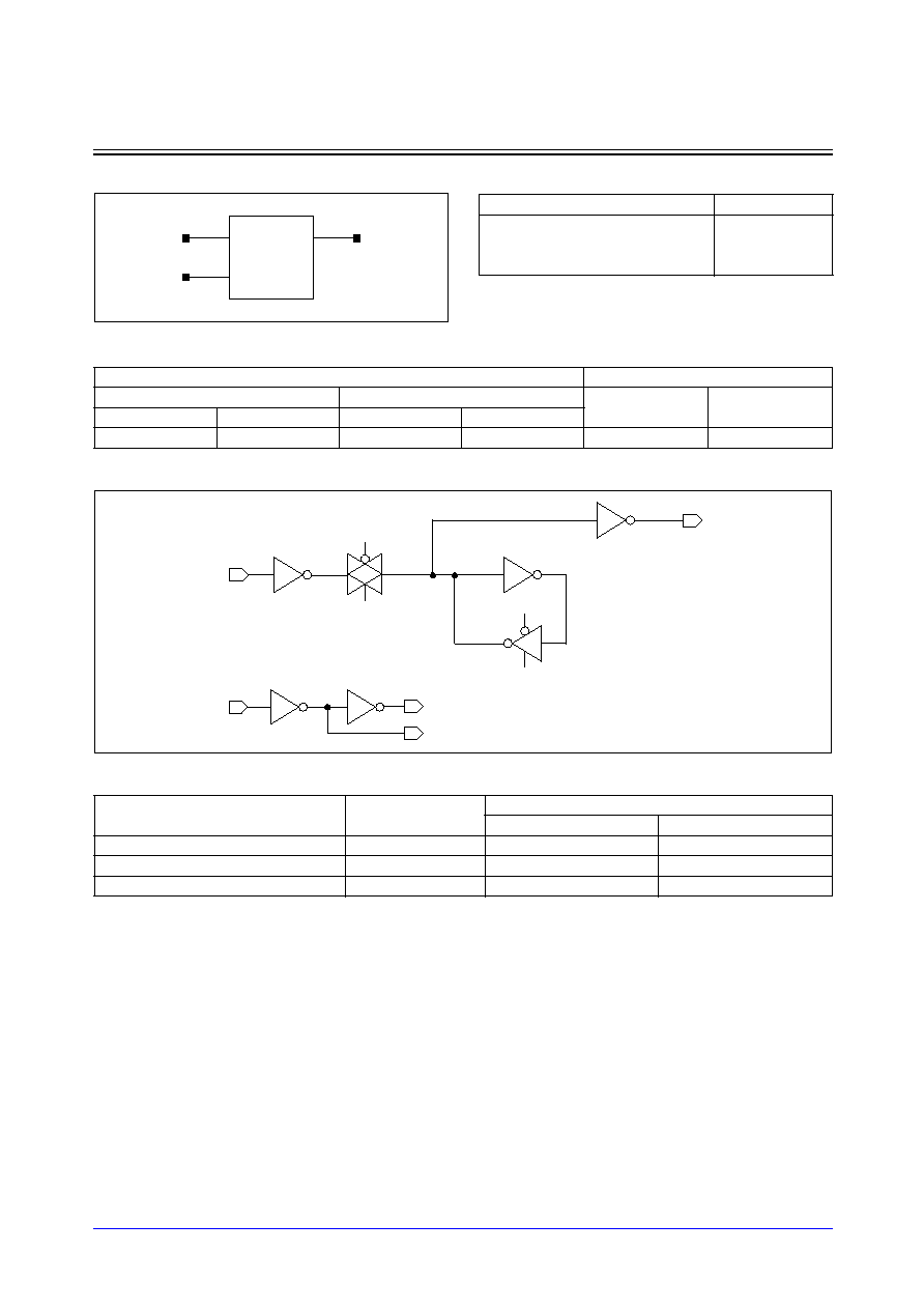
Samsung ASIC
3-299
STDL131
LD1Q_LP/LD1QD2_LP
D Latch with Active High, Q Output Only, 1X/2X Drive
Logic Symbol
Cell Data
Schematic Diagram
Timing Requirements
(Typical process, 25
∞
C, 1.8V, Unit = ns)
Input Load (SL)
Gate Count
LD1Q_LP
LD1QD2_LP
LD1Q_LP
LD1QD2_LP
D
G
D
G
1.1
1.1
1.1
1.1
3.67
3.67
Parameter
Symbol
Value (ns)
LD1Q_LP
LD1QD2_LP
Input Setup Time (D to G)
t
SU
0.127
0.159
Input Hold Time (D to G)
t
HD
0.013
0.010
Pulse Width High (G)
t
PWH
0.149
0.188
D
G
Q
GL
G
GB
D
Q
GL
GB
GL
GB
Truth Table
D
G
Q (n+1)
0
1
0
1
1
1
x
0
Q (n)
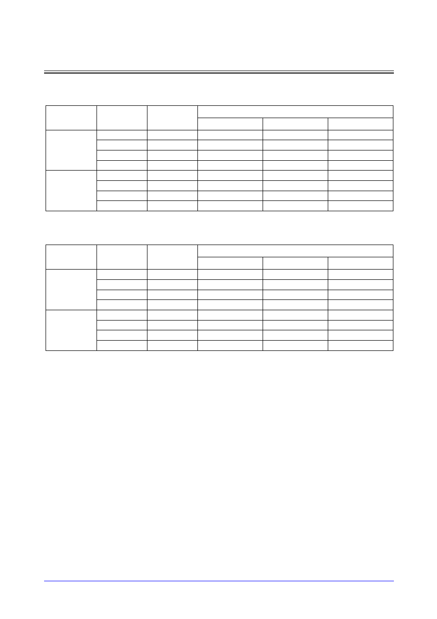
STDL131
3-300
Samsung ASIC
LD1Q_LP/LD1QD2_LP
D Latch with Active High, Q Output Only, 1X/2X Drive
Switching Characteristics
(Typical process, 25
∞
C, 1.8V, t
R
/t
F
= 0.19ns, SL: Standard Load)
LD1Q_LP
LD1QD2_LP
Path
Parameter
Delay [ns]
SL = 2
Delay Equations [ns]
Group1*
Group2*
Group3*
D to Q
tR
0.108
0.060 + 0.024*SL
0.055 + 0.025*SL
0.052 + 0.026*SL
tF
0.097
0.062 + 0.017*SL
0.067 + 0.016*SL
0.065 + 0.016*SL
tPLH
0.196
0.166 + 0.015*SL
0.173 + 0.013*SL
0.177 + 0.012*SL
tPHL
0.228
0.199 + 0.015*SL
0.211 + 0.012*SL
0.222 + 0.010*SL
G to Q
tR
0.108
0.059 + 0.024*SL
0.055 + 0.025*SL
0.051 + 0.026*SL
tF
0.096
0.061 + 0.017*SL
0.065 + 0.016*SL
0.066 + 0.016*SL
tPLH
0.232
0.203 + 0.015*SL
0.209 + 0.013*SL
0.213 + 0.012*SL
tPHL
0.246
0.216 + 0.015*SL
0.229 + 0.012*SL
0.239 + 0.010*SL
*Group1 : SL < 4, *Group2 : 4 SL
<
<
=
= 8, *Group3 : 8 < SL
Path
Parameter
Delay [ns]
SL = 2
Delay Equations [ns]
Group1*
Group2*
Group3*
D to Q
tR
0.082
0.054 + 0.014*SL
0.059 + 0.012*SL
0.054 + 0.013*SL
tF
0.083
0.060 + 0.012*SL
0.072 + 0.009*SL
0.077 + 0.008*SL
tPLH
0.198
0.179 + 0.010*SL
0.188 + 0.007*SL
0.200 + 0.006*SL
tPHL
0.232
0.211 + 0.010*SL
0.223 + 0.007*SL
0.244 + 0.006*SL
G to Q
tR
0.081
0.054 + 0.014*SL
0.058 + 0.012*SL
0.053 + 0.013*SL
tF
0.083
0.061 + 0.011*SL
0.070 + 0.009*SL
0.076 + 0.008*SL
tPLH
0.233
0.214 + 0.010*SL
0.223 + 0.007*SL
0.235 + 0.006*SL
tPHL
0.254
0.233 + 0.011*SL
0.245 + 0.007*SL
0.266 + 0.006*SL
*Group1 : SL < 4, *Group2 : 4 SL
<
<
=
= 12, *Group3 : 12 < SL
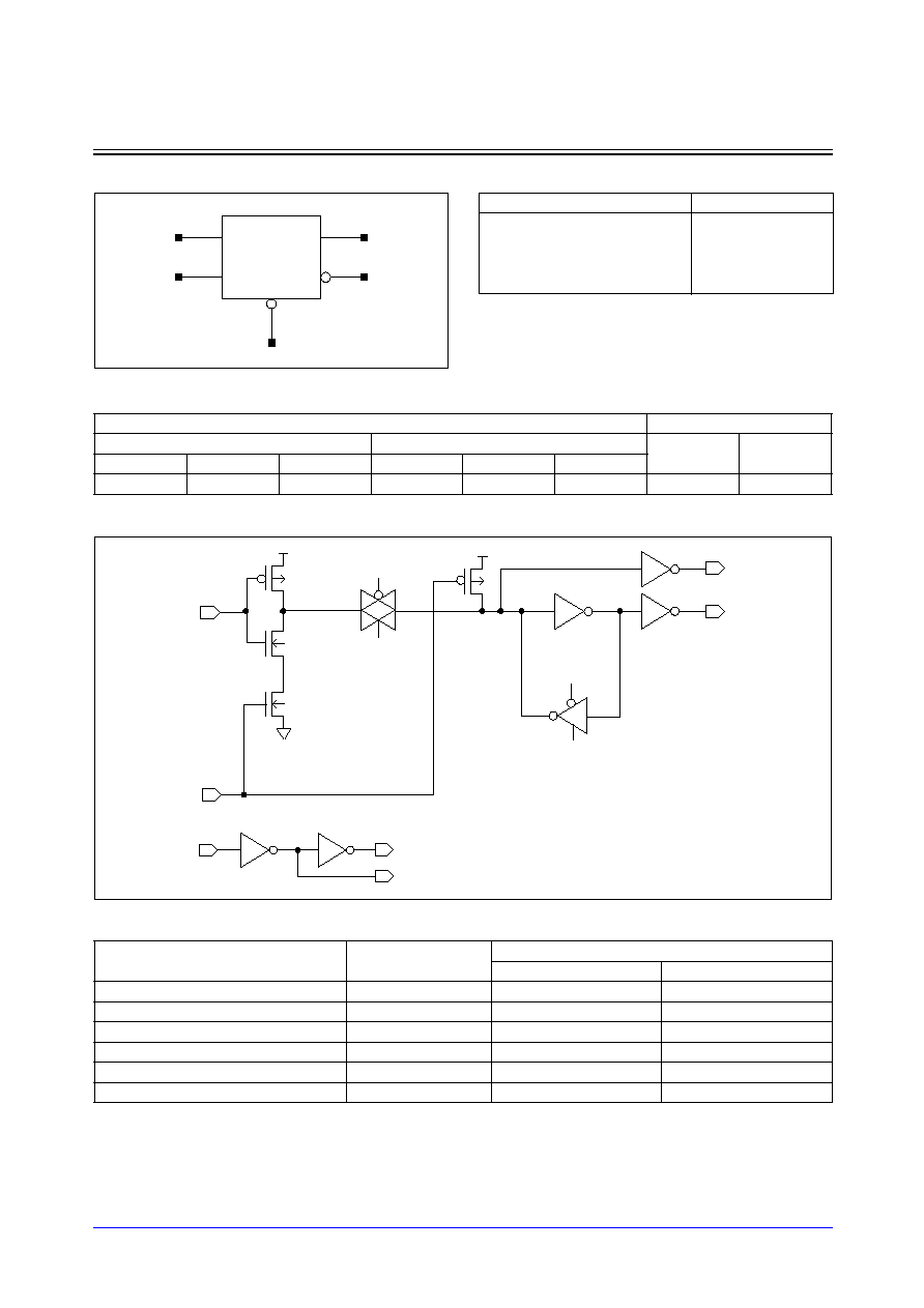
Samsung ASIC
3-301
STDL131
LD2_LP/LD2D2_LP
D Latch with Active High, Reset, 1X/2X Drive
Logic Symbol
Cell Data
Schematic Diagram
Timing Requirements
(Typical process, 25
∞
C, 1.8V, Unit = ns)
Input Load (SL)
Gate Count
LD2_LP
LD2D2_LP
LD2_LP
LD2D2_LP
D
G
RN
D
G
RN
1.1
1.1
0.7
1.1
1.1
0.8
4.67
4.67
Parameter
Symbol
Value (ns)
LD2_LP
LD2D2_LP
Input Setup Time (D to G)
t
SU
0.150
0.208
Input Hold Time (D to G)
t
HD
0.010
0.010
Pulse Width High (G)
t
PWH
0.187
0.252
Pulse Width Low (RN)
t
PWL
0.295
0.283
Recovery Time (RN to G)
t
RC
0.085
0.134
Removal Time (RN to G)
t
RM
0.010
0.010
D
G
Q
QN
RN
GL
G
GB
D
Q
QN
RN
GL
GB
GL
GB
Truth Table
D
G
RN
Q (n+1) QN (n+1)
0
1
1
0
1
1
1
1
1
0
x
0
1
Q (n)
QN (n)
x
x
0
0
1

STDL131
3-302
Samsung ASIC
LD2_LP/LD2D2_LP
D Latch with Active High, Reset, 1X/2X Drive
Switching Characteristics
(Typical process, 25
∞
C, 1.8V, t
R
/t
F
= 0.19ns, SL: Standard Load)
LD2_LP
Path
Parameter
Delay [ns]
SL = 2
Delay Equations [ns]
Group1*
Group2*
Group3*
D to Q
tR
0.122
0.070 + 0.026*SL
0.073 + 0.025*SL
0.071 + 0.025*SL
tF
0.100
0.063 + 0.018*SL
0.070 + 0.017*SL
0.074 + 0.016*SL
tPLH
0.253
0.219 + 0.017*SL
0.230 + 0.014*SL
0.240 + 0.013*SL
tPHL
0.239
0.207 + 0.016*SL
0.220 + 0.012*SL
0.234 + 0.011*SL
G to Q
tR
0.121
0.069 + 0.026*SL
0.073 + 0.025*SL
0.070 + 0.025*SL
tF
0.099
0.061 + 0.019*SL
0.071 + 0.016*SL
0.071 + 0.016*SL
tPLH
0.267
0.233 + 0.017*SL
0.244 + 0.014*SL
0.254 + 0.013*SL
tPHL
0.261
0.230 + 0.016*SL
0.243 + 0.012*SL
0.256 + 0.010*SL
RN to Q
tR
0.122
0.070 + 0.026*SL
0.073 + 0.025*SL
0.071 + 0.025*SL
tF
0.120
0.076 + 0.022*SL
0.093 + 0.018*SL
0.104 + 0.016*SL
tPLH
0.247
0.213 + 0.017*SL
0.224 + 0.014*SL
0.234 + 0.013*SL
tPHL
0.309
0.272 + 0.019*SL
0.288 + 0.015*SL
0.309 + 0.012*SL
D to QN
tR
0.097
0.049 + 0.024*SL
0.042 + 0.026*SL
0.039 + 0.026*SL
tF
0.073
0.040 + 0.016*SL
0.040 + 0.016*SL
0.037 + 0.017*SL
tPLH
0.307
0.281 + 0.013*SL
0.283 + 0.012*SL
0.284 + 0.012*SL
tPHL
0.314
0.291 + 0.011*SL
0.297 + 0.010*SL
0.301 + 0.009*SL
G to QN
tR
0.097
0.049 + 0.024*SL
0.043 + 0.026*SL
0.039 + 0.026*SL
tF
0.073
0.041 + 0.016*SL
0.038 + 0.017*SL
0.036 + 0.017*SL
tPLH
0.329
0.303 + 0.013*SL
0.306 + 0.013*SL
0.306 + 0.012*SL
tPHL
0.328
0.305 + 0.011*SL
0.311 + 0.010*SL
0.314 + 0.009*SL
RN to QN
tR
0.100
0.052 + 0.024*SL
0.046 + 0.026*SL
0.042 + 0.026*SL
tF
0.074
0.042 + 0.016*SL
0.041 + 0.016*SL
0.037 + 0.017*SL
tPLH
0.382
0.355 + 0.013*SL
0.359 + 0.012*SL
0.359 + 0.012*SL
tPHL
0.308
0.285 + 0.011*SL
0.291 + 0.010*SL
0.295 + 0.009*SL
*Group1 : SL < 4, *Group2 : 4 SL
<
<
=
= 8, *Group3 : 8 < SL
Samsung ASIC
3-303
STDL131
LD2_LP/LD2D2_LP
D Latch with Active High, Reset, 1X/2X Drive
Switching Characteristics
(Typical process, 25
∞
C, 1.8V, t
R
/t
F
= 0.19ns, SL: Standard Load)
LD2D2_LP
Path
Parameter
Delay [ns]
SL = 2
Delay Equations [ns]
Group1*
Group2*
Group3*
D to Q
tR
0.101
0.072 + 0.015*SL
0.078 + 0.013*SL
0.084 + 0.013*SL
tF
0.089
0.066 + 0.012*SL
0.076 + 0.009*SL
0.088 + 0.008*SL
tPLH
0.267
0.244 + 0.012*SL
0.256 + 0.009*SL
0.276 + 0.007*SL
tPHL
0.251
0.229 + 0.011*SL
0.242 + 0.008*SL
0.265 + 0.006*SL
G to Q
tR
0.101
0.073 + 0.014*SL
0.077 + 0.013*SL
0.083 + 0.013*SL
tF
0.090
0.067 + 0.011*SL
0.075 + 0.009*SL
0.089 + 0.008*SL
tPLH
0.278
0.254 + 0.012*SL
0.267 + 0.009*SL
0.286 + 0.007*SL
tPHL
0.275
0.252 + 0.011*SL
0.266 + 0.008*SL
0.289 + 0.006*SL
RN to Q
tR
0.101
0.073 + 0.014*SL
0.077 + 0.013*SL
0.084 + 0.013*SL
tF
0.090
0.067 + 0.012*SL
0.073 + 0.010*SL
0.093 + 0.008*SL
tPLH
0.262
0.238 + 0.012*SL
0.251 + 0.009*SL
0.270 + 0.007*SL
tPHL
0.274
0.251 + 0.012*SL
0.264 + 0.008*SL
0.288 + 0.006*SL
D to QN
tR
0.071
0.048 + 0.011*SL
0.045 + 0.012*SL
0.036 + 0.013*SL
tF
0.058
0.040 + 0.009*SL
0.043 + 0.008*SL
0.039 + 0.008*SL
tPLH
0.354
0.338 + 0.008*SL
0.344 + 0.007*SL
0.347 + 0.006*SL
tPHL
0.364
0.349 + 0.007*SL
0.357 + 0.006*SL
0.365 + 0.005*SL
G to QN
tR
0.071
0.048 + 0.011*SL
0.045 + 0.012*SL
0.036 + 0.013*SL
tF
0.058
0.040 + 0.009*SL
0.044 + 0.008*SL
0.038 + 0.008*SL
tPLH
0.377
0.361 + 0.008*SL
0.367 + 0.007*SL
0.370 + 0.006*SL
tPHL
0.375
0.360 + 0.007*SL
0.367 + 0.006*SL
0.376 + 0.005*SL
RN to QN
tR
0.073
0.051 + 0.011*SL
0.046 + 0.012*SL
0.036 + 0.013*SL
tF
0.059
0.042 + 0.009*SL
0.045 + 0.008*SL
0.040 + 0.008*SL
tPLH
0.376
0.360 + 0.008*SL
0.366 + 0.007*SL
0.369 + 0.006*SL
tPHL
0.358
0.343 + 0.008*SL
0.351 + 0.006*SL
0.359 + 0.005*SL
*Group1 : SL < 4, *Group2 : 4 SL
<
<
=
= 12, *Group3 : 12 < SL
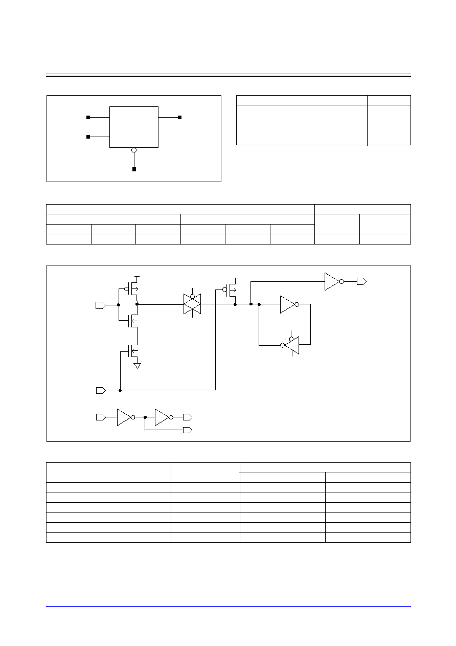
STDL131
3-304
Samsung ASIC
LD2Q_LP/LD2QD2_LP
D Latch with Active High, Reset, Q Output Only, 1X/2X Drive
Logic Symbol
Cell Data
Schematic Diagram
Timing Requirements
(Typical process, 25
∞
C, 1.8V, Unit = ns)
Input Load (SL)
Gate Count
LD2Q_LP
LD2QD2_LP
LD2Q_LP
LD2QD2_LP
D
G
RN
D
G
RN
1.1
1.1
0.8
1.1
1.1
0.9
4.00
4.33
Parameter
Symbol
Value (ns)
LD2Q_LP
LD2QD2_LP
Input Setup Time (D to G)
t
SU
0.133
0.173
Input Hold Time (D to G)
t
HD
0.010
0.010
Pulse Width High (G)
t
PWH
0.157
0.196
Pulse Width Low (RN)
t
PWL
0.240
0.213
Recovery Time (RN to G)
t
RC
0.073
0.103
Removal Time (RN to G)
t
RM
0.010
0.010
D
G
Q
RN
GL
G
GB
D
Q
RN
GB
GL
GL
GB
Truth Table
D
G
RN
Q (n+1)
0
1
1
0
1
1
1
1
x
0
1
Q (n)
x
x
0
0

Samsung ASIC
3-305
STDL131
LD2Q_LP/LD2QD2_LP
D Latch with Active High, Reset, Q Output Only, 1X/2X Drive
Switching Characteristics
(Typical process, 25
∞
C, 1.8V, t
R
/t
F
= 0.19ns, SL: Standard Load)
LD2Q_LP
LD2QD2_LP
Path
Parameter
Delay [ns]
SL = 2
Delay Equations [ns]
Group1*
Group2*
Group3*
D to Q
tR
0.121
0.071 + 0.025*SL
0.071 + 0.025*SL
0.067 + 0.025*SL
tF
0.098
0.063 + 0.017*SL
0.067 + 0.017*SL
0.070 + 0.016*SL
tPLH
0.245
0.211 + 0.017*SL
0.223 + 0.014*SL
0.232 + 0.013*SL
tPHL
0.233
0.203 + 0.015*SL
0.216 + 0.012*SL
0.228 + 0.010*SL
G to Q
tR
0.120
0.070 + 0.025*SL
0.071 + 0.025*SL
0.067 + 0.025*SL
tF
0.096
0.061 + 0.018*SL
0.065 + 0.017*SL
0.069 + 0.016*SL
tPLH
0.257
0.223 + 0.017*SL
0.234 + 0.014*SL
0.244 + 0.013*SL
tPHL
0.252
0.221 + 0.015*SL
0.234 + 0.012*SL
0.246 + 0.010*SL
RN to Q
tR
0.121
0.072 + 0.025*SL
0.071 + 0.025*SL
0.068 + 0.025*SL
tF
0.120
0.078 + 0.021*SL
0.091 + 0.018*SL
0.101 + 0.016*SL
tPLH
0.238
0.205 + 0.017*SL
0.216 + 0.014*SL
0.225 + 0.013*SL
tPHL
0.301
0.264 + 0.018*SL
0.281 + 0.014*SL
0.301 + 0.012*SL
*Group1 : SL < 4, *Group2 : 4 SL
<
<
=
= 8, *Group3 : 8 < SL
Path
Parameter
Delay [ns]
SL = 2
Delay Equations [ns]
Group1*
Group2*
Group3*
D to Q
tR
0.097
0.067 + 0.015*SL
0.077 + 0.013*SL
0.077 + 0.013*SL
tF
0.087
0.064 + 0.011*SL
0.075 + 0.009*SL
0.082 + 0.008*SL
tPLH
0.252
0.230 + 0.011*SL
0.241 + 0.008*SL
0.260 + 0.007*SL
tPHL
0.240
0.219 + 0.011*SL
0.232 + 0.007*SL
0.253 + 0.006*SL
G to Q
tR
0.096
0.066 + 0.015*SL
0.075 + 0.013*SL
0.077 + 0.013*SL
tF
0.086
0.064 + 0.011*SL
0.073 + 0.009*SL
0.080 + 0.008*SL
tPLH
0.262
0.240 + 0.011*SL
0.251 + 0.008*SL
0.270 + 0.007*SL
tPHL
0.260
0.239 + 0.011*SL
0.252 + 0.007*SL
0.273 + 0.006*SL
RN to Q
tR
0.098
0.069 + 0.015*SL
0.077 + 0.013*SL
0.077 + 0.013*SL
tF
0.088
0.064 + 0.012*SL
0.074 + 0.009*SL
0.088 + 0.008*SL
tPLH
0.246
0.224 + 0.011*SL
0.236 + 0.008*SL
0.254 + 0.007*SL
tPHL
0.262
0.240 + 0.011*SL
0.252 + 0.008*SL
0.275 + 0.006*SL
*Group1 : SL < 4, *Group2 : 4 SL
<
<
=
= 12, *Group3 : 12 < SL
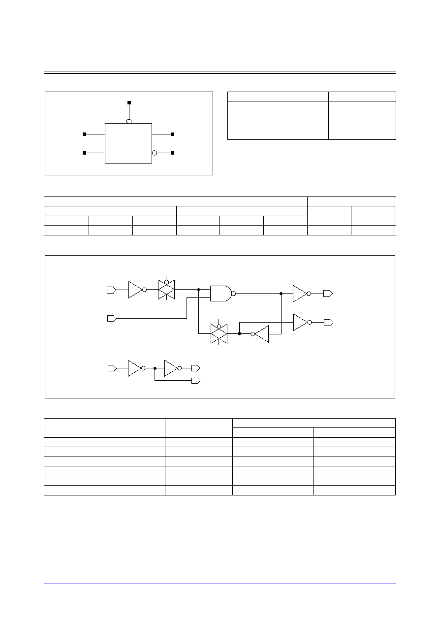
STDL131
3-306
Samsung ASIC
LD3_LP/LD3D2_LP
D Latch with Active High, Set, 1X/2X Drive
Logic Symbol
Cell Data
Schematic Diagram
Timing Requirements
(Typical process, 25
∞
C, 1.8V, Unit = ns)
Input Load (SL)
Gate Count
LD3_LP
LD3D2_LP
LD3_LP
LD3D2_LP
D
G
SN
D
G
SN
1.1
1.1
1.1
1.1
1.1
1.1
4.67
5.33
Parameter
Symbol
Value (ns)
LD3_LP
LD3D2_LP
Input Setup Time (D to G)
t
SU
0.134
0.152
Input Hold Time (D to G)
t
HD
0.010
0.010
Pulse Width High (G)
t
PWH
0.160
0.183
Pulse Width Low (SN)
t
PWL
0.188
0.233
Recovery Time (SN to G)
t
RC
0.010
0.010
Removal Time (SN to G)
t
RM
0.105
0.076
D
G
Q
QN
SN
GL
G
GB
D
GB
GL
GB
QN
Q
SN
GL
Truth Table
D
G
SN
Q (n+1) QN (n+1)
0
1
1
0
1
1
1
1
1
0
x
0
1
Q (n)
QN (n)
x
x
0
1
0

Samsung ASIC
3-307
STDL131
LD3_LP/LD3D2_LP
D Latch with Active High, Set, 1X/2X Drive
Switching Characteristics
(Typical process, 25
∞
C, 1.8V, t
R
/t
F
= 0.19ns, SL: Standard Load)
LD3_LP
Path
Parameter
Delay [ns]
SL = 2
Delay Equations [ns]
Group1*
Group2*
Group3*
D to Q
tR
0.093
0.042 + 0.026*SL
0.040 + 0.026*SL
0.035 + 0.027*SL
tF
0.071
0.036 + 0.017*SL
0.038 + 0.017*SL
0.034 + 0.017*SL
tPLH
0.313
0.287 + 0.013*SL
0.289 + 0.013*SL
0.290 + 0.013*SL
tPHL
0.359
0.336 + 0.011*SL
0.342 + 0.010*SL
0.345 + 0.010*SL
G to Q
tR
0.093
0.043 + 0.025*SL
0.037 + 0.026*SL
0.036 + 0.027*SL
tF
0.072
0.040 + 0.016*SL
0.039 + 0.017*SL
0.034 + 0.017*SL
tPLH
0.354
0.328 + 0.013*SL
0.330 + 0.013*SL
0.331 + 0.013*SL
tPHL
0.378
0.355 + 0.011*SL
0.361 + 0.010*SL
0.364 + 0.010*SL
SN to Q
tR
0.093
0.043 + 0.025*SL
0.038 + 0.026*SL
0.035 + 0.027*SL
tF
0.072
0.039 + 0.016*SL
0.038 + 0.017*SL
0.033 + 0.017*SL
tPLH
0.245
0.218 + 0.013*SL
0.220 + 0.013*SL
0.221 + 0.013*SL
tPHL
0.229
0.206 + 0.011*SL
0.211 + 0.010*SL
0.214 + 0.010*SL
D to QN
tR
0.102
0.052 + 0.025*SL
0.051 + 0.025*SL
0.045 + 0.026*SL
tF
0.074
0.039 + 0.017*SL
0.042 + 0.017*SL
0.040 + 0.017*SL
tPLH
0.298
0.268 + 0.015*SL
0.275 + 0.013*SL
0.279 + 0.013*SL
tPHL
0.250
0.225 + 0.012*SL
0.232 + 0.011*SL
0.238 + 0.010*SL
G to QN
tR
0.103
0.052 + 0.025*SL
0.052 + 0.025*SL
0.045 + 0.026*SL
tF
0.075
0.041 + 0.017*SL
0.041 + 0.017*SL
0.040 + 0.017*SL
tPLH
0.317
0.287 + 0.015*SL
0.294 + 0.013*SL
0.298 + 0.013*SL
tPHL
0.291
0.266 + 0.012*SL
0.273 + 0.011*SL
0.279 + 0.010*SL
SN to QN
tR
0.101
0.050 + 0.025*SL
0.051 + 0.025*SL
0.045 + 0.026*SL
tF
0.077
0.043 + 0.017*SL
0.043 + 0.017*SL
0.040 + 0.017*SL
tPLH
0.167
0.138 + 0.015*SL
0.144 + 0.013*SL
0.148 + 0.013*SL
tPHL
0.181
0.156 + 0.012*SL
0.164 + 0.011*SL
0.170 + 0.010*SL
*Group1 : SL < 4, *Group2 : 4 SL
<
<
=
= 8, *Group3 : 8 < SL

STDL131
3-308
Samsung ASIC
LD3_LP/LD3D2_LP
D Latch with Active High, Reset, 1X/2X Drive
Switching Characteristics
(Typical process, 25
∞
C, 1.8V, t
R
/t
F
= 0.19ns, SL: Standard Load)
LD3D2_LP
Path
Parameter
Delay [ns]
SL = 2
Delay Equations [ns]
Group1*
Group2*
Group3*
D to Q
tR
0.066
0.043 + 0.012*SL
0.038 + 0.013*SL
0.031 + 0.013*SL
tF
0.056
0.038 + 0.009*SL
0.041 + 0.008*SL
0.036 + 0.008*SL
tPLH
0.340
0.325 + 0.008*SL
0.329 + 0.007*SL
0.332 + 0.006*SL
tPHL
0.394
0.379 + 0.007*SL
0.386 + 0.006*SL
0.394 + 0.005*SL
G to Q
tR
0.066
0.043 + 0.012*SL
0.038 + 0.013*SL
0.031 + 0.013*SL
tF
0.055
0.038 + 0.008*SL
0.039 + 0.008*SL
0.035 + 0.008*SL
tPLH
0.383
0.368 + 0.008*SL
0.372 + 0.007*SL
0.375 + 0.006*SL
tPHL
0.414
0.400 + 0.007*SL
0.406 + 0.006*SL
0.414 + 0.005*SL
SN to Q
tR
0.065
0.040 + 0.012*SL
0.038 + 0.013*SL
0.031 + 0.013*SL
tF
0.055
0.037 + 0.009*SL
0.040 + 0.008*SL
0.035 + 0.008*SL
tPLH
0.271
0.256 + 0.008*SL
0.260 + 0.007*SL
0.263 + 0.006*SL
tPHL
0.261
0.246 + 0.007*SL
0.253 + 0.006*SL
0.261 + 0.005*SL
D to QN
tR
0.082
0.057 + 0.013*SL
0.057 + 0.012*SL
0.054 + 0.013*SL
tF
0.062
0.043 + 0.009*SL
0.046 + 0.009*SL
0.049 + 0.008*SL
tPLH
0.310
0.291 + 0.010*SL
0.300 + 0.007*SL
0.310 + 0.006*SL
tPHL
0.259
0.243 + 0.008*SL
0.251 + 0.006*SL
0.263 + 0.005*SL
G to QN
tR
0.081
0.055 + 0.013*SL
0.056 + 0.013*SL
0.054 + 0.013*SL
tF
0.061
0.043 + 0.009*SL
0.046 + 0.009*SL
0.048 + 0.008*SL
tPLH
0.330
0.311 + 0.010*SL
0.320 + 0.007*SL
0.330 + 0.006*SL
tPHL
0.302
0.285 + 0.008*SL
0.294 + 0.006*SL
0.305 + 0.005*SL
SN to QN
tR
0.080
0.055 + 0.013*SL
0.055 + 0.013*SL
0.053 + 0.013*SL
tF
0.063
0.044 + 0.009*SL
0.047 + 0.008*SL
0.049 + 0.008*SL
tPLH
0.177
0.158 + 0.009*SL
0.167 + 0.007*SL
0.177 + 0.006*SL
tPHL
0.190
0.173 + 0.008*SL
0.182 + 0.006*SL
0.194 + 0.005*SL
*Group1 : SL < 4, *Group2 : 4 SL
<
<
=
= 12, *Group3 : 12 < SL
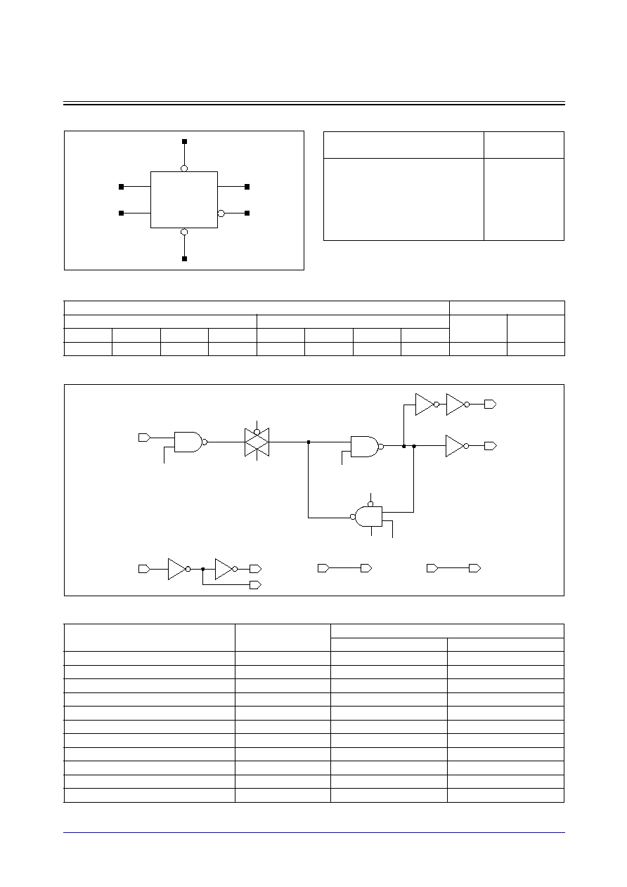
Samsung ASIC
3-309
STDL131
LD4_LP/LD4D2_LP
D Latch with Active High, Reset, Set, 1X/2X Drive
Logic Symbol
Cell Data
Schematic Diagram
Timing Requirements
(Typical process, 25
∞
C, 1.8V, Unit = ns)
Input Load (SL)
Gate Count
LD4_LP
LD4D2_LP
LD4_LP
LD4D2_LP
D
G
SN
RN
D
G
SN
RN
1.1
1.1
1.1
1.3
1.1
1.2
1.1
1.4
6.00
6.33
Parameter
Symbol
Value (ns)
LD4_LP
LD4D2_LP
Input Setup Time (D to G)
t
SU
0.159
0.161
Input Hold Time (D to G)
t
HD
0.010
0.010
Pulse Width High (G)
t
PWH
0.145
0.151
Pulse Width Low (SN)
t
PWL
0.307
0.329
Recovery Time (SN to G)
t
RC
0.010
0.010
Removal Time (SN to G)
t
RM
0.231
0.209
Pulse Width Low (RN)
t
PWL
1.049
1.080
Recovery Time (RN to G)
t
RC
0.079
0.081
Removal Time (RN to G)
t
RM
0.010
0.010
Recovery Time (SN to RN)
t
RC
0.010
0.010
Removal Time (SN to RN)
t
RM
0.119
0.092
D
G
Q
QN
SN
RN
GL
G
GB
D
QN
Q
RN
SN
RN
RN
SN
SN
GL
GB
RN
GL
GB
Truth Table
D
G
RN
SN
Q
(n+1)
QN
(n+1)
0
1
1
1
0
1
1
1
1
1
1
0
x
0
1
1
Q (n)
QN (n)
x
x
1
0
1
0
x
x
0
1
0
1
x
x
0
0
1
0

STDL131
3-310
Samsung ASIC
LD4_LP/LD4D2_LP
D Latch with Active High, Reset, Set, 1X/2X Drive
Switching Characteristics
(Typical process, 25
∞
C, 1.8V, t
R
/t
F
= 0.19ns, SL: Standard Load)
LD4_LP
Path
Parameter
Delay [ns]
SL = 2
Delay Equations [ns]
Group1*
Group2*
Group3*
D to Q
tR
0.091
0.042 + 0.025*SL
0.035 + 0.026*SL
0.034 + 0.027*SL
tF
0.071
0.039 + 0.016*SL
0.038 + 0.017*SL
0.032 + 0.017*SL
tPLH
0.371
0.345 + 0.013*SL
0.347 + 0.013*SL
0.348 + 0.012*SL
tPHL
0.397
0.374 + 0.011*SL
0.380 + 0.010*SL
0.382 + 0.010*SL
G to Q
tR
0.091
0.040 + 0.025*SL
0.035 + 0.026*SL
0.035 + 0.027*SL
tF
0.070
0.036 + 0.017*SL
0.035 + 0.017*SL
0.033 + 0.017*SL
tPLH
0.370
0.344 + 0.013*SL
0.346 + 0.013*SL
0.346 + 0.013*SL
tPHL
0.388
0.365 + 0.011*SL
0.370 + 0.010*SL
0.373 + 0.010*SL
SN to Q
tR
0.091
0.041 + 0.025*SL
0.035 + 0.027*SL
0.035 + 0.027*SL
tF
0.071
0.038 + 0.017*SL
0.036 + 0.017*SL
0.033 + 0.017*SL
tPLH
0.248
0.221 + 0.013*SL
0.224 + 0.013*SL
0.224 + 0.013*SL
tPHL
0.234
0.211 + 0.011*SL
0.217 + 0.010*SL
0.219 + 0.010*SL
RN to Q
tR
0.092
0.041 + 0.025*SL
0.039 + 0.026*SL
0.033 + 0.027*SL
tF
0.071
0.039 + 0.016*SL
0.037 + 0.017*SL
0.033 + 0.017*SL
tPLH
0.367
0.341 + 0.013*SL
0.343 + 0.013*SL
0.344 + 0.013*SL
tPHL
0.406
0.383 + 0.011*SL
0.388 + 0.010*SL
0.391 + 0.010*SL
D to QN
tR
0.106
0.056 + 0.025*SL
0.054 + 0.025*SL
0.049 + 0.026*SL
tF
0.077
0.042 + 0.018*SL
0.047 + 0.016*SL
0.043 + 0.017*SL
tPLH
0.339
0.309 + 0.015*SL
0.317 + 0.013*SL
0.321 + 0.013*SL
tPHL
0.312
0.286 + 0.013*SL
0.295 + 0.011*SL
0.302 + 0.010*SL
G to QN
tR
0.105
0.054 + 0.025*SL
0.053 + 0.025*SL
0.049 + 0.026*SL
tF
0.077
0.042 + 0.017*SL
0.044 + 0.017*SL
0.043 + 0.017*SL
tPLH
0.330
0.300 + 0.015*SL
0.307 + 0.013*SL
0.312 + 0.013*SL
tPHL
0.311
0.285 + 0.013*SL
0.293 + 0.011*SL
0.300 + 0.010*SL
SN to QN
tR
0.103
0.053 + 0.025*SL
0.051 + 0.026*SL
0.047 + 0.026*SL
tF
0.078
0.043 + 0.017*SL
0.046 + 0.016*SL
0.042 + 0.017*SL
tPLH
0.177
0.147 + 0.015*SL
0.154 + 0.013*SL
0.158 + 0.013*SL
tPHL
0.189
0.163 + 0.013*SL
0.171 + 0.011*SL
0.178 + 0.010*SL
RN to QN
tR
0.106
0.056 + 0.025*SL
0.055 + 0.025*SL
0.049 + 0.026*SL
tF
0.078
0.043 + 0.017*SL
0.046 + 0.017*SL
0.043 + 0.017*SL
tPLH
0.348
0.318 + 0.015*SL
0.325 + 0.013*SL
0.330 + 0.013*SL
tPHL
0.308
0.283 + 0.013*SL
0.291 + 0.011*SL
0.298 + 0.010*SL
*Group1 : SL < 4, *Group2 : 4 SL
<
<
=
= 8, *Group3 : 8 < SL

Samsung ASIC
3-311
STDL131
LD4_LP/LD4D2_LP
D Latch with Active High, Reset, Set, 1X/2X Drive
Switching Characteristics
(Typical process, 25
∞
C, 1.8V, t
R
/t
F
= 0.19ns, SL: Standard Load)
LD4D2_LP
Path
Parameter
Delay [ns]
SL = 2
Delay Equations [ns]
Group1*
Group2*
Group3*
D to Q
tR
0.066
0.043 + 0.011*SL
0.038 + 0.013*SL
0.031 + 0.013*SL
tF
0.056
0.040 + 0.008*SL
0.041 + 0.008*SL
0.036 + 0.008*SL
tPLH
0.402
0.387 + 0.008*SL
0.391 + 0.007*SL
0.394 + 0.006*SL
tPHL
0.430
0.415 + 0.007*SL
0.422 + 0.006*SL
0.430 + 0.005*SL
G to Q
tR
0.066
0.043 + 0.011*SL
0.038 + 0.013*SL
0.031 + 0.013*SL
tF
0.056
0.041 + 0.008*SL
0.038 + 0.008*SL
0.035 + 0.008*SL
tPLH
0.402
0.387 + 0.008*SL
0.391 + 0.007*SL
0.394 + 0.006*SL
tPHL
0.423
0.408 + 0.007*SL
0.415 + 0.006*SL
0.423 + 0.005*SL
SN to Q
tR
0.066
0.043 + 0.011*SL
0.038 + 0.013*SL
0.031 + 0.013*SL
tF
0.056
0.040 + 0.008*SL
0.040 + 0.008*SL
0.035 + 0.008*SL
tPLH
0.278
0.262 + 0.008*SL
0.267 + 0.007*SL
0.270 + 0.006*SL
tPHL
0.266
0.251 + 0.007*SL
0.258 + 0.006*SL
0.266 + 0.005*SL
RN to Q
tR
0.066
0.043 + 0.011*SL
0.038 + 0.013*SL
0.031 + 0.013*SL
tF
0.056
0.040 + 0.008*SL
0.040 + 0.008*SL
0.035 + 0.008*SL
tPLH
0.398
0.383 + 0.008*SL
0.387 + 0.007*SL
0.390 + 0.006*SL
tPHL
0.439
0.425 + 0.007*SL
0.432 + 0.006*SL
0.440 + 0.005*SL
D to QN
tR
0.083
0.057 + 0.013*SL
0.059 + 0.013*SL
0.056 + 0.013*SL
tF
0.063
0.045 + 0.009*SL
0.047 + 0.009*SL
0.051 + 0.008*SL
tPLH
0.343
0.324 + 0.010*SL
0.333 + 0.007*SL
0.344 + 0.007*SL
tPHL
0.318
0.301 + 0.008*SL
0.310 + 0.006*SL
0.323 + 0.005*SL
G to QN
tR
0.082
0.056 + 0.013*SL
0.058 + 0.013*SL
0.055 + 0.013*SL
tF
0.063
0.045 + 0.009*SL
0.047 + 0.009*SL
0.051 + 0.008*SL
tPLH
0.336
0.317 + 0.010*SL
0.326 + 0.007*SL
0.337 + 0.007*SL
tPHL
0.317
0.300 + 0.009*SL
0.309 + 0.006*SL
0.322 + 0.005*SL
SN to QN
tR
0.081
0.055 + 0.013*SL
0.056 + 0.013*SL
0.054 + 0.013*SL
tF
0.062
0.043 + 0.010*SL
0.047 + 0.009*SL
0.050 + 0.008*SL
tPLH
0.180
0.161 + 0.010*SL
0.170 + 0.007*SL
0.180 + 0.007*SL
tPHL
0.194
0.177 + 0.008*SL
0.186 + 0.006*SL
0.198 + 0.005*SL
RN to QN
tR
0.083
0.057 + 0.013*SL
0.059 + 0.013*SL
0.056 + 0.013*SL
tF
0.063
0.043 + 0.010*SL
0.048 + 0.009*SL
0.051 + 0.008*SL
tPLH
0.353
0.333 + 0.010*SL
0.343 + 0.007*SL
0.354 + 0.007*SL
tPHL
0.314
0.297 + 0.009*SL
0.306 + 0.006*SL
0.319 + 0.005*SL
*Group1 : SL < 4, *Group2 : 4 SL
<
<
=
= 12, *Group3 : 12 < SL
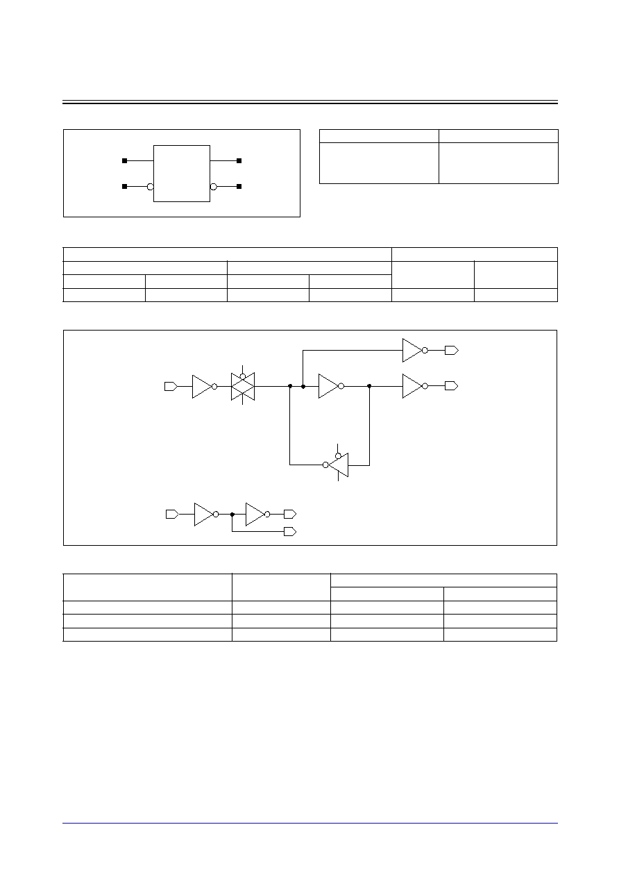
STDL131
3-312
Samsung ASIC
LD5_LP/LD5D2_LP
D Latch with Active Low, 1X/2X Drive
Logic Symbol
Cell Data
Schematic Diagram
Timing Requirements
(Typical process, 25
∞
C, 1.8V, Unit = ns)
Input Load (SL)
Gate Count
LD5_LP
LD5D2_LP
LD5_LP
LD5D2_LP
D
GN
D
GN
1.1
1.2
1.2
1.1
4.33
4.67
Parameter
Symbol
Value (ns)
LD5_LP
LD5D2_LP
Input Setup Time (D to GN)
t
SU
0.121
0.152
Input Hold Time (D to GN)
t
HD
0.010
0.010
Pulse Width Low (GN)
t
PWL
0.161
0.220
D
GN
Q
QN
QN
Q
D
GNB
GLN
GLN
GN
GNB
GNB
GLN
Truth Table
D
GN
Q (n+1)
QN (n+1)
0
0
0
1
1
0
1
0
x
1
Q (n)
QN (n)
Samsung ASIC
3-313
STDL131
LD5_LP/LD5D2_LP
D Latch with Active Low, 1X/2X Drive
Switching Characteristics
(Typical process, 25
∞
C, 1.8V, t
R
/t
F
= 0.19ns, SL: Standard Load)
LD5_LP
LD5D2_LP
Path
Parameter
Delay [ns]
SL = 2
Delay Equations [ns]
Group1*
Group2*
Group3*
D to Q
tR
0.106
0.056 + 0.025*SL
0.055 + 0.025*SL
0.050 + 0.026*SL
tF
0.097
0.060 + 0.019*SL
0.067 + 0.017*SL
0.068 + 0.017*SL
tPLH
0.198
0.168 + 0.015*SL
0.175 + 0.013*SL
0.180 + 0.013*SL
tPHL
0.230
0.200 + 0.015*SL
0.212 + 0.012*SL
0.225 + 0.011*SL
GN to Q
tR
0.106
0.055 + 0.025*SL
0.056 + 0.025*SL
0.050 + 0.026*SL
tF
0.096
0.059 + 0.019*SL
0.066 + 0.017*SL
0.067 + 0.017*SL
tPLH
0.241
0.211 + 0.015*SL
0.218 + 0.013*SL
0.223 + 0.013*SL
tPHL
0.277
0.246 + 0.015*SL
0.258 + 0.012*SL
0.271 + 0.010*SL
D to QN
tR
0.097
0.048 + 0.024*SL
0.043 + 0.026*SL
0.037 + 0.026*SL
tF
0.070
0.037 + 0.016*SL
0.036 + 0.017*SL
0.035 + 0.017*SL
tPLH
0.298
0.271 + 0.013*SL
0.274 + 0.013*SL
0.275 + 0.012*SL
tPHL
0.257
0.235 + 0.011*SL
0.240 + 0.010*SL
0.243 + 0.009*SL
GN to QN
tR
0.095
0.046 + 0.025*SL
0.041 + 0.026*SL
0.039 + 0.026*SL
tF
0.070
0.037 + 0.017*SL
0.038 + 0.016*SL
0.034 + 0.017*SL
tPLH
0.344
0.318 + 0.013*SL
0.320 + 0.012*SL
0.321 + 0.012*SL
tPHL
0.300
0.278 + 0.011*SL
0.283 + 0.010*SL
0.286 + 0.009*SL
*Group1 : SL < 4, *Group2 : 4 SL
<
<
=
= 8, *Group3 : 8 < SL
Path
Parameter
Delay [ns]
SL = 2
Delay Equations [ns]
Group1*
Group2*
Group3*
D to Q
tR
0.086
0.060 + 0.013*SL
0.062 + 0.013*SL
0.060 + 0.013*SL
tF
0.088
0.067 + 0.011*SL
0.072 + 0.009*SL
0.085 + 0.008*SL
tPLH
0.207
0.187 + 0.010*SL
0.197 + 0.008*SL
0.208 + 0.007*SL
tPHL
0.244
0.223 + 0.011*SL
0.235 + 0.008*SL
0.256 + 0.006*SL
GN to Q
tR
0.086
0.060 + 0.013*SL
0.062 + 0.013*SL
0.060 + 0.013*SL
tF
0.088
0.067 + 0.010*SL
0.071 + 0.009*SL
0.085 + 0.008*SL
tPLH
0.255
0.235 + 0.010*SL
0.245 + 0.008*SL
0.256 + 0.007*SL
tPHL
0.292
0.270 + 0.011*SL
0.283 + 0.008*SL
0.304 + 0.006*SL
D to QN
tR
0.071
0.048 + 0.011*SL
0.044 + 0.012*SL
0.036 + 0.013*SL
tF
0.054
0.036 + 0.009*SL
0.040 + 0.008*SL
0.036 + 0.008*SL
tPLH
0.343
0.328 + 0.008*SL
0.333 + 0.007*SL
0.336 + 0.006*SL
tPHL
0.293
0.279 + 0.007*SL
0.285 + 0.006*SL
0.293 + 0.005*SL
GN to QN
tR
0.071
0.048 + 0.011*SL
0.043 + 0.013*SL
0.036 + 0.013*SL
tF
0.054
0.037 + 0.008*SL
0.038 + 0.008*SL
0.034 + 0.009*SL
tPLH
0.391
0.375 + 0.008*SL
0.381 + 0.007*SL
0.384 + 0.006*SL
tPHL
0.341
0.326 + 0.007*SL
0.333 + 0.006*SL
0.341 + 0.005*SL
*Group1 : SL < 4, *Group2 : 4 SL
<
<
=
= 12, *Group3 : 12 < SL
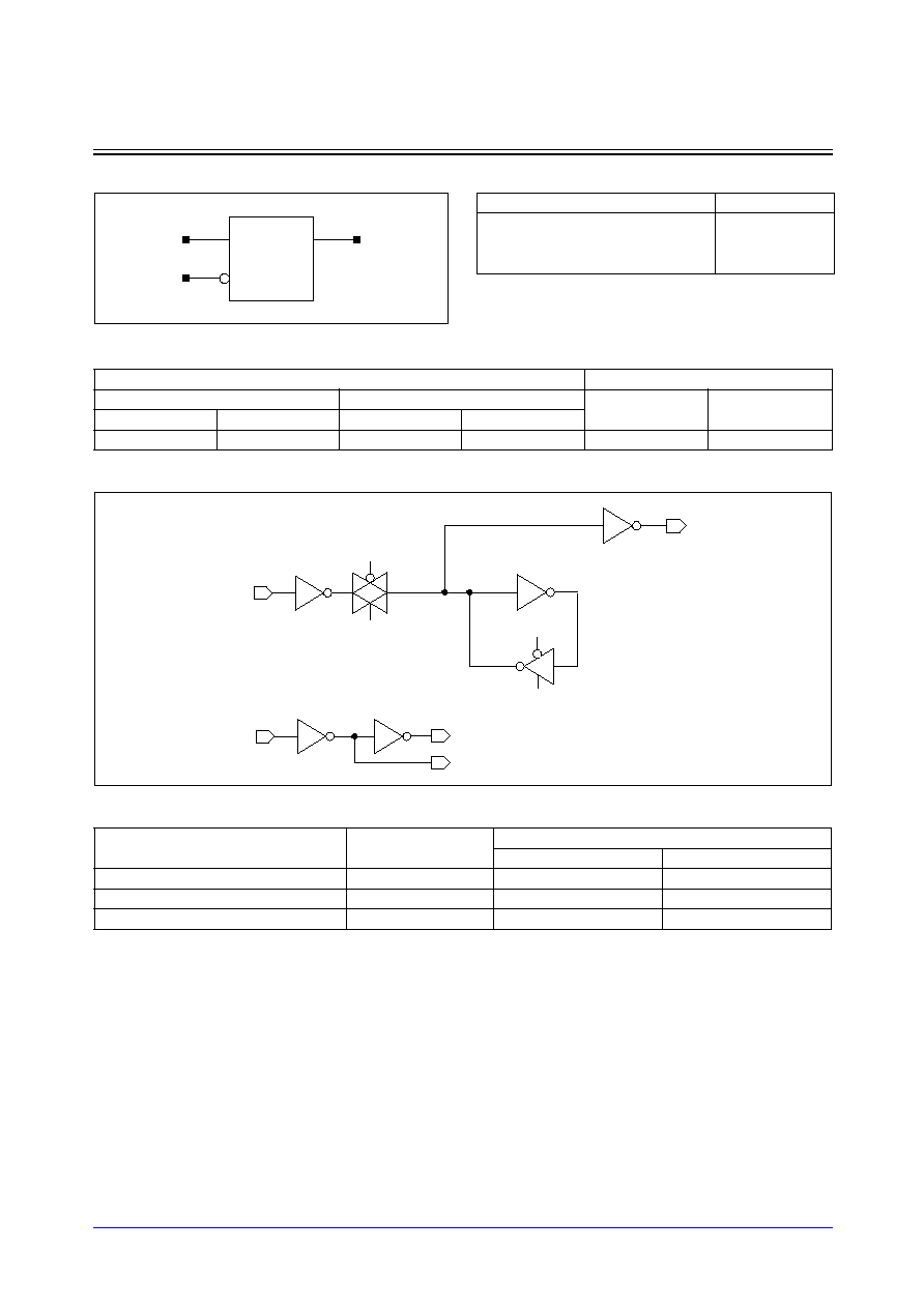
STDL131
3-314
Samsung ASIC
LD5Q_LP/LD5QD2_LP
D Latch with Active Low, Q Output Only, 1X/2X Drive
Logic Symbol
Cell Data
Schematic Diagram
Timing Requirements
(Typical process, 25
∞
C, 1.8V, Unit = ns)
Input Load (SL)
Gate Count
LD5Q_LP
LD5QD2_LP
LD5Q_LP
LD5QD2_LP
D
GN
D
GN
1.1
1.1
1.1
1.1
3.67
4.00
Parameter
Symbol
Value (ns)
LD5Q_LP
LD5QD2_LP
Input Setup Time (D to GN)
t
SU
0.113
0.133
Input Hold Time (D to GN)
t
HD
0.010
0.010
Pulse Width Low (GN)
t
PWL
0.140
0.169
D
GN
Q
Q
D
GNB
GLN
GLN
GN
GNB
GLN
GNB
Truth Table
D
GN
Q (n+1)
0
0
0
1
0
1
x
1
Q (n)
Samsung ASIC
3-315
STDL131
LD5Q_LP/LD5QD2_LP
D Latch with Active Low, Q Output Only, 1X/2X Drive
Switching Characteristics
(Typical process, 25
∞
C, 1.8V, t
R
/t
F
= 0.19ns, SL: Standard Load)
LD5Q_LP
LD5QD2_LP
Path
Parameter
Delay [ns]
SL = 2
Delay Equations [ns]
Group1*
Group2*
Group3*
D to Q
tR
0.107
0.058 + 0.024*SL
0.055 + 0.025*SL
0.049 + 0.026*SL
tF
0.096
0.060 + 0.018*SL
0.067 + 0.016*SL
0.065 + 0.016*SL
tPLH
0.196
0.166 + 0.015*SL
0.173 + 0.013*SL
0.178 + 0.012*SL
tPHL
0.227
0.198 + 0.015*SL
0.210 + 0.012*SL
0.222 + 0.010*SL
GN to Q
tR
0.106
0.057 + 0.024*SL
0.053 + 0.025*SL
0.050 + 0.026*SL
tF
0.094
0.058 + 0.018*SL
0.066 + 0.016*SL
0.064 + 0.016*SL
tPLH
0.239
0.209 + 0.015*SL
0.217 + 0.013*SL
0.221 + 0.012*SL
tPHL
0.271
0.242 + 0.015*SL
0.254 + 0.012*SL
0.266 + 0.010*SL
*Group1 : SL < 4, *Group2 : 4 SL
<
<
=
= 8, *Group3 : 8 < SL
Path
Parameter
Delay [ns]
SL = 2
Delay Equations [ns]
Group1*
Group2*
Group3*
D to Q
tR
0.082
0.056 + 0.013*SL
0.059 + 0.012*SL
0.054 + 0.013*SL
tF
0.086
0.064 + 0.011*SL
0.072 + 0.009*SL
0.078 + 0.008*SL
tPLH
0.197
0.179 + 0.009*SL
0.187 + 0.007*SL
0.198 + 0.006*SL
tPHL
0.235
0.214 + 0.010*SL
0.226 + 0.007*SL
0.247 + 0.006*SL
GN to Q
tR
0.082
0.056 + 0.013*SL
0.059 + 0.012*SL
0.054 + 0.013*SL
tF
0.084
0.061 + 0.011*SL
0.073 + 0.009*SL
0.076 + 0.008*SL
tPLH
0.243
0.224 + 0.010*SL
0.233 + 0.007*SL
0.244 + 0.006*SL
tPHL
0.279
0.258 + 0.010*SL
0.270 + 0.007*SL
0.291 + 0.006*SL
*Group1 : SL < 4, *Group2 : 4 SL
<
<
=
= 12, *Group3 : 12 < SL
STDL131
3-316
Samsung ASIC
LD6_LP/LD6D2_LP
D Latch with Active Low, Reset, 1X/2X Drive
Logic Symbol
Cell Data
Schematic Diagram
Timing Requirements
(Typical process, 25
∞
C, 1.8V, Unit = ns)
Input Load (SL)
Gate Count
LD6_LP
LD6D2_LP
LD6_LP
LD6D2_LP
D
GN
RN
D
GN
RN
1.1
1.2
0.7
1.1
1.1
0.8
4.67
5.00
Parameter
Symbol
Value (ns)
LD6_LP
LD6D2_LP
Input Setup Time (D to GN)
t
SU
0.183
0.235
Input Hold Time (D to GN)
t
HD
0.010
0.010
Pulse Width Low (GN)
t
PWL
0.190
0.254
Pulse Width Low (RN)
t
PWL
0.294
0.284
Recovery Time (RN to GN)
t
RC
0.180
0.232
Removal Time (RN to GN)
t
RM
0.010
0.010
D
GN
Q
QN
RN
GLN
GN
GNB
RN
D
Q
GLN
GNB
QN
GNB
GLN
Truth Table
D
GN
RN
Q (n+1) QN (n+1)
0
0
1
0
1
1
0
1
1
0
x
1
1
Q (n)
QN (n)
x
x
0
0
1

Samsung ASIC
3-317
STDL131
LD6_LP/LD6D2_LP
D Latch with Active Low, Reset, 1X/2X Drive
Switching Characteristics
(Typical process, 25
∞
C, 1.8V, t
R
/t
F
= 0.19ns, SL: Standard Load)
LD6_LP
Path
Parameter
Delay [ns]
SL = 2
Delay Equations [ns]
Group1*
Group2*
Group3*
D to Q
tR
0.121
0.069 + 0.026*SL
0.073 + 0.025*SL
0.071 + 0.025*SL
tF
0.100
0.063 + 0.018*SL
0.070 + 0.017*SL
0.074 + 0.016*SL
tPLH
0.253
0.218 + 0.017*SL
0.230 + 0.014*SL
0.240 + 0.013*SL
tPHL
0.238
0.207 + 0.016*SL
0.220 + 0.012*SL
0.234 + 0.011*SL
GN to Q
tR
0.121
0.069 + 0.026*SL
0.074 + 0.025*SL
0.070 + 0.025*SL
tF
0.098
0.060 + 0.019*SL
0.070 + 0.017*SL
0.071 + 0.016*SL
tPLH
0.274
0.240 + 0.017*SL
0.251 + 0.014*SL
0.262 + 0.013*SL
tPHL
0.285
0.254 + 0.016*SL
0.267 + 0.012*SL
0.281 + 0.011*SL
RN to Q
tR
0.121
0.069 + 0.026*SL
0.073 + 0.025*SL
0.071 + 0.025*SL
tF
0.120
0.075 + 0.022*SL
0.092 + 0.018*SL
0.104 + 0.016*SL
tPLH
0.247
0.213 + 0.017*SL
0.224 + 0.014*SL
0.234 + 0.013*SL
tPHL
0.309
0.271 + 0.019*SL
0.287 + 0.015*SL
0.309 + 0.012*SL
D to QN
tR
0.097
0.048 + 0.024*SL
0.041 + 0.026*SL
0.038 + 0.027*SL
tF
0.072
0.040 + 0.016*SL
0.038 + 0.016*SL
0.036 + 0.017*SL
tPLH
0.307
0.281 + 0.013*SL
0.283 + 0.013*SL
0.284 + 0.013*SL
tPHL
0.314
0.291 + 0.011*SL
0.297 + 0.010*SL
0.300 + 0.009*SL
GN to QN
tR
0.096
0.046 + 0.025*SL
0.041 + 0.026*SL
0.037 + 0.027*SL
tF
0.072
0.039 + 0.016*SL
0.038 + 0.016*SL
0.036 + 0.017*SL
tPLH
0.354
0.327 + 0.013*SL
0.330 + 0.013*SL
0.331 + 0.013*SL
tPHL
0.336
0.313 + 0.011*SL
0.319 + 0.010*SL
0.322 + 0.009*SL
RN to QN
tR
0.099
0.050 + 0.024*SL
0.044 + 0.026*SL
0.040 + 0.026*SL
tF
0.073
0.041 + 0.016*SL
0.041 + 0.016*SL
0.034 + 0.017*SL
tPLH
0.382
0.355 + 0.014*SL
0.358 + 0.013*SL
0.359 + 0.013*SL
tPHL
0.308
0.285 + 0.011*SL
0.291 + 0.010*SL
0.295 + 0.009*SL
*Group1 : SL < 4, *Group2 : 4 SL
<
<
=
= 8, *Group3 : 8 < SL

STDL131
3-318
Samsung ASIC
LD6_LP/LD6D2_LP
D Latch with Active Low, Reset, 1X/2X Drive
Switching Characteristics
(Typical process, 25
∞
C, 1.8V, t
R
/t
F
= 0.19ns, SL: Standard Load)
LD6D2_LP
Path
Parameter
Delay [ns]
SL = 2
Delay Equations [ns]
Group1*
Group2*
Group3*
D to Q
tR
0.101
0.073 + 0.014*SL
0.077 + 0.013*SL
0.083 + 0.013*SL
tF
0.090
0.068 + 0.011*SL
0.073 + 0.009*SL
0.088 + 0.008*SL
tPLH
0.266
0.242 + 0.012*SL
0.255 + 0.009*SL
0.274 + 0.007*SL
tPHL
0.249
0.227 + 0.011*SL
0.240 + 0.008*SL
0.263 + 0.006*SL
GN to Q
tR
0.101
0.073 + 0.014*SL
0.077 + 0.013*SL
0.083 + 0.013*SL
tF
0.089
0.066 + 0.011*SL
0.074 + 0.009*SL
0.086 + 0.008*SL
tPLH
0.294
0.271 + 0.012*SL
0.283 + 0.009*SL
0.302 + 0.007*SL
tPHL
0.301
0.278 + 0.011*SL
0.292 + 0.008*SL
0.314 + 0.006*SL
RN to Q
tR
0.101
0.073 + 0.014*SL
0.077 + 0.013*SL
0.083 + 0.013*SL
tF
0.090
0.066 + 0.012*SL
0.073 + 0.010*SL
0.091 + 0.008*SL
tPLH
0.260
0.237 + 0.012*SL
0.249 + 0.009*SL
0.268 + 0.007*SL
tPHL
0.271
0.249 + 0.011*SL
0.261 + 0.008*SL
0.285 + 0.006*SL
D to QN
tR
0.073
0.051 + 0.011*SL
0.045 + 0.012*SL
0.037 + 0.013*SL
tF
0.060
0.042 + 0.009*SL
0.045 + 0.008*SL
0.040 + 0.008*SL
tPLH
0.357
0.341 + 0.008*SL
0.347 + 0.007*SL
0.350 + 0.006*SL
tPHL
0.369
0.354 + 0.008*SL
0.361 + 0.006*SL
0.371 + 0.005*SL
GN to QN
tR
0.072
0.049 + 0.012*SL
0.046 + 0.012*SL
0.037 + 0.013*SL
tF
0.060
0.042 + 0.009*SL
0.046 + 0.008*SL
0.039 + 0.008*SL
tPLH
0.408
0.392 + 0.008*SL
0.398 + 0.007*SL
0.401 + 0.006*SL
tPHL
0.397
0.382 + 0.008*SL
0.389 + 0.006*SL
0.399 + 0.005*SL
RN to QN
tR
0.074
0.051 + 0.011*SL
0.047 + 0.012*SL
0.037 + 0.013*SL
tF
0.061
0.043 + 0.009*SL
0.047 + 0.008*SL
0.043 + 0.008*SL
tPLH
0.379
0.362 + 0.008*SL
0.368 + 0.007*SL
0.372 + 0.006*SL
tPHL
0.363
0.348 + 0.008*SL
0.355 + 0.006*SL
0.365 + 0.005*SL
*Group1 : SL < 4, *Group2 : 4 SL
<
<
=
= 12, *Group3 : 12 < SL
Samsung ASIC
3-319
STDL131
LD6Q_LP/LD6QD2_LP
D Latch with Active Low, Reset, Q Output Only, 1X/2X Drive
Logic Symbol
Cell Data
Schematic Diagram
Timing Requirements
(Typical process, 25
∞
C, 1.8V, Unit = ns)
Input Load (SL)
Gate Count
LD6Q_LP
LD6QD2_LP
LD6Q_LP
LD6QD2_LP
D
GN
RN
D
GN
RN
1.1
1.2
0.7
1.1
1.1
0.8
4.00
4.33
Parameter
Symbol
Value (ns)
LD6Q_LP
LD6QD2_LP
Input Setup Time (D to GN)
t
SU
0.167
0.208
Input Hold Time (D to GN)
t
HD
0.010
0.010
Pulse Width Low (GN)
t
PWL
0.165
0.213
Pulse Width Low (RN)
t
PWL
0.233
0.220
Recovery Time (RN to GN)
t
RC
0.162
0.202
Removal Time (RN to GN)
t
RM
0.010
0.010
D
GN
Q
RN
GLN
GN
GNB
D
Q
GLN
GNB
GLN
GNB
RN
Truth Table
D
GN
RN
Q (n+1)
0
0
1
0
1
0
1
1
x
1
1
Q (n)
x
x
0
0

STDL131
3-320
Samsung ASIC
LD6Q_LP/LD6QD2_LP
D Latch with Active Low, Reset, Q Output Only, 1X/2X Drive
Switching Characteristics
(Typical process, 25
∞
C, 1.8V, t
R
/t
F
= 0.19ns, SL: Standard Load)
LD6Q_LP
LD6QD2_LP
Path
Parameter
Delay [ns]
SL = 2
Delay Equations [ns]
Group1*
Group2*
Group3*
D to Q
tR
0.119
0.067 + 0.026*SL
0.069 + 0.025*SL
0.064 + 0.026*SL
tF
0.097
0.060 + 0.018*SL
0.067 + 0.017*SL
0.068 + 0.017*SL
tPLH
0.243
0.209 + 0.017*SL
0.220 + 0.014*SL
0.230 + 0.013*SL
tPHL
0.231
0.200 + 0.016*SL
0.214 + 0.012*SL
0.226 + 0.010*SL
GN to Q
tR
0.118
0.067 + 0.026*SL
0.068 + 0.025*SL
0.064 + 0.026*SL
tF
0.096
0.060 + 0.018*SL
0.066 + 0.017*SL
0.067 + 0.017*SL
tPLH
0.264
0.230 + 0.017*SL
0.242 + 0.014*SL
0.251 + 0.013*SL
tPHL
0.277
0.246 + 0.016*SL
0.260 + 0.012*SL
0.273 + 0.010*SL
RN to Q
tR
0.119
0.068 + 0.025*SL
0.069 + 0.025*SL
0.064 + 0.026*SL
tF
0.118
0.076 + 0.021*SL
0.088 + 0.018*SL
0.099 + 0.017*SL
tPLH
0.236
0.202 + 0.017*SL
0.214 + 0.014*SL
0.223 + 0.013*SL
tPHL
0.298
0.260 + 0.019*SL
0.277 + 0.015*SL
0.298 + 0.012*SL
*Group1 : SL < 4, *Group2 : 4 SL
<
<
=
= 8, *Group3 : 8 < SL
Path
Parameter
Delay [ns]
SL = 2
Delay Equations [ns]
Group1*
Group2*
Group3*
D to Q
tR
0.097
0.066 + 0.015*SL
0.077 + 0.013*SL
0.078 + 0.013*SL
tF
0.087
0.065 + 0.011*SL
0.074 + 0.009*SL
0.082 + 0.008*SL
tPLH
0.256
0.233 + 0.011*SL
0.245 + 0.008*SL
0.264 + 0.007*SL
tPHL
0.240
0.219 + 0.011*SL
0.232 + 0.008*SL
0.254 + 0.006*SL
GN to Q
tR
0.097
0.066 + 0.015*SL
0.076 + 0.013*SL
0.078 + 0.013*SL
tF
0.087
0.063 + 0.012*SL
0.074 + 0.009*SL
0.082 + 0.008*SL
tPLH
0.283
0.260 + 0.011*SL
0.272 + 0.008*SL
0.291 + 0.007*SL
tPHL
0.290
0.269 + 0.011*SL
0.282 + 0.008*SL
0.304 + 0.006*SL
RN to Q
tR
0.098
0.068 + 0.015*SL
0.077 + 0.013*SL
0.078 + 0.013*SL
tF
0.088
0.063 + 0.013*SL
0.076 + 0.009*SL
0.088 + 0.008*SL
tPLH
0.250
0.227 + 0.011*SL
0.239 + 0.008*SL
0.258 + 0.007*SL
tPHL
0.264
0.242 + 0.011*SL
0.254 + 0.008*SL
0.278 + 0.006*SL
*Group1 : SL < 4, *Group2 : 4 SL
<
<
=
= 12, *Group3 : 12 < SL
Samsung ASIC
3-321
STDL130
BUSHOLDER
Cell List
Logic Symbol
Cell Name
Function Description
BUSHOLDER_LP
Bus Holder
Y
Cell Data
Input Load (SL)
Gate Count
Y
1.33
6.4
STDL130
3-322
Samsung ASIC
INTERNAL CLOCK DRIVERS
Cell List
Logic Symbol
Cell Data
Cell Name
Function Description
CK2_LP
Internal Clock Driver CMOS 2mA
CK4_LP
Internal Clock Driver CMOS 4mA
CK6_LP
Internal Clock Driver CMOS 6mA
CK8_LP
Internal Clock Driver CMOS 8mA
Standard Load (SL)
I/O Slot
CK2
CK4
CK6
CK8
CK2
CK4
CK6
CK8
A
A
A
A
12.81
12.68
25.81
25.70
1.0
1.0
1.0
1.0
Truth Table
A
Y
0
1
0
1
Y
A

Samsung ASIC
3-323
STDL130
CK2_LP/CK4_LP/CK6_LP/CK8_LP
Internal Clock Driver CMOS 2/4/6/8mA
Switching Characteristics
(Typical process, 25
∞
C, 1.8V, t
R
/t
F
= 0.20ns, SL: Standard Load)
CK2_LP
CK4_LP
CK6_LP
CK8_LP
Path
Parameter
Delay [ns]
SL = 2
Delay Equations [ns]
Group1*
Group2*
Group3*
A to Y
tR
0.038
0.034 + 0.002*SL
0.032 + 0.002*SL
0.031 + 0.002*SL
tF
0.035
0.032 + 0.002*SL
0.028 + 0.002*SL
0.028 + 0.002*SL
tPLH
0.133
0.132 + 0.001*SL
0.132 + 0.001*SL
0.132 + 0.001*SL
tPHL
0.146
0.144 + 0.001*SL
0.145 + 0.001*SL
0.146 + 0.001*SL
*Group1 : SL < 292, *Group2 : 292 SL
<
<
=
= 438, *Group3 : 438 < SL
Path
Parameter
Delay [ns]
SL = 2
Delay Equations [ns]
Group1*
Group2*
Group3*
A to Y
tR
0.044
0.042 + 0.001*SL
0.037 + 0.001*SL
0.035 + 0.001*SL
tF
0.040
0.039 + 0.001*SL
0.034 + 0.001*SL
0.032 + 0.001*SL
tPLH
0.167
0.166 + 0.000*SL
0.166 + 0.000*SL
0.167 + 0.000*SL
tPHL
0.178
0.177 + 0.000*SL
0.179 + 0.000*SL
0.179 + 0.000*SL
*Group1 : SL < 584, *Group2 : 584 SL
<
<
=
= 875, *Group3 : 875 < SL
Path
Parameter
Delay [ns]
SL = 2
Delay Equations [ns]
Group1*
Group2*
Group3*
A to Y
tR
0.039
0.037 + 0.001*SL
0.034 + 0.001*SL
0.033 + 0.001*SL
tF
0.036
0.035 + 0.001*SL
0.031 + 0.001*SL
0.030 + 0.001*SL
tPLH
0.150
0.149 + 0.000*SL
0.150 + 0.000*SL
0.150 + 0.000*SL
tPHL
0.162
0.161 + 0.000*SL
0.162 + 0.000*SL
0.163 + 0.000*SL
*Group1 : SL < 876, *Group2 : 876 SL
<
<
=
= 1314, *Group3 : 1314 < SL
Path
Parameter
Delay [ns]
SL = 2
Delay Equations [ns]
Group1*
Group2*
Group3*
A to Y
tR
0.043
0.042 + 0.000*SL
0.037 + 0.000*SL
0.035 + 0.000*SL
tF
0.040
0.039 + 0.000*SL
0.034 + 0.000*SL
0.032 + 0.000*SL
tPLH
0.166
0.166 + 0.000*SL
0.166 + 0.000*SL
0.167 + 0.000*SL
tPHL
0.178
0.177 + 0.000*SL
0.179 + 0.000*SL
0.179 + 0.000*SL
*Group1 : SL < 1166, *Group2 : 1166 SL
<
<
=
= 1749, *Group3 : 1749 < SL

STDL130
3-324
Samsung ASIC
ADDERS
Cell List
Cell Name
Function Description
FA_LP
Full Adder with 1X Drive
FAD2_LP
Full Adder with 2X Drive
HA_LP
Half Adder with 1x Drive
HAD2_LP
Half Adder with 2X Drive
Samsung ASIC
3-325
STDL130
FA_LP/FAD2_LP
Full Adder with 1X/2X Drive
Logic Symbol
Cell Data
Switching Characteristics
(Typical process, 25
∞
C, 1.8V, t
R
/t
F
= 0.22ns, SL: Standard Load)
FA_LP
Input Load (SL)
Gate Count
FA_LP
FAD2_LP
FA_LP
FAD2_LP
CI
A
B
CI
A
B
1.0
1.1
1.1
1.0
1.1
1.0
9.00
9.67
CI
A
B
S
CO
Path
Parameter
Delay [ns]
SL = 2
Delay Equations [ns]
Group1*
Group2*
Group3*
A to S
tR
0.122
0.068 + 0.027*SL
0.061 + 0.029*SL
0.057 + 0.029*SL
tF
0.105
0.063 + 0.021*SL
0.069 + 0.020*SL
0.067 + 0.020*SL
tPLH
0.442
0.409 + 0.017*SL
0.417 + 0.015*SL
0.421 + 0.014*SL
tPHL
0.469
0.435 + 0.017*SL
0.448 + 0.014*SL
0.458 + 0.012*SL
B to S
tR
0.123
0.069 + 0.027*SL
0.065 + 0.028*SL
0.057 + 0.029*SL
tF
0.106
0.064 + 0.021*SL
0.069 + 0.020*SL
0.068 + 0.020*SL
tPLH
0.532
0.498 + 0.017*SL
0.507 + 0.015*SL
0.510 + 0.014*SL
tPHL
0.553
0.520 + 0.017*SL
0.532 + 0.014*SL
0.542 + 0.012*SL
CI to S
tR
0.118
0.062 + 0.028*SL
0.060 + 0.028*SL
0.053 + 0.029*SL
tF
0.111
0.069 + 0.021*SL
0.074 + 0.020*SL
0.073 + 0.020*SL
tPLH
0.361
0.328 + 0.017*SL
0.336 + 0.015*SL
0.340 + 0.014*SL
tPHL
0.350
0.315 + 0.017*SL
0.329 + 0.014*SL
0.339 + 0.012*SL
A to CO
tR
0.122
0.067 + 0.027*SL
0.063 + 0.028*SL
0.056 + 0.029*SL
tF
0.107
0.064 + 0.022*SL
0.070 + 0.020*SL
0.070 + 0.020*SL
tPLH
0.438
0.404 + 0.017*SL
0.413 + 0.015*SL
0.417 + 0.014*SL
tPHL
0.469
0.435 + 0.017*SL
0.447 + 0.014*SL
0.458 + 0.013*SL
B to CO
tR
0.170
0.127 + 0.021*SL
0.116 + 0.024*SL
0.090 + 0.028*SL
tF
0.131
0.097 + 0.017*SL
0.093 + 0.018*SL
0.085 + 0.019*SL
tPLH
0.521
0.488 + 0.017*SL
0.496 + 0.015*SL
0.500 + 0.014*SL
tPHL
0.557
0.524 + 0.017*SL
0.536 + 0.014*SL
0.546 + 0.013*SL
CI to CO
tR
0.118
0.062 + 0.028*SL
0.060 + 0.029*SL
0.054 + 0.029*SL
tF
0.111
0.068 + 0.021*SL
0.075 + 0.020*SL
0.074 + 0.020*SL
tPLH
0.252
0.218 + 0.017*SL
0.226 + 0.015*SL
0.230 + 0.014*SL
tPHL
0.286
0.252 + 0.017*SL
0.265 + 0.014*SL
0.277 + 0.012*SL
*Group1 : SL < 4, *Group2 : 4 SL
<
<
=
= 7, *Group3 : 7 < SL
Truth Table
CI
A
B
S
CO
0
0
0
0
0
1
0
0
1
0
0
0
1
1
0
1
0
1
0
1
0
1
0
1
0
1
1
0
0
1
0
1
1
0
1
1
1
1
1
1

STDL130
3-326
Samsung ASIC
FA_LP/FAD2_LP
Full Adder with 1X/2X Drive
Switching Characteristics
(Typical process, 25
∞
C, 1.8V, t
R
/t
F
= 0.22ns, SL: Standard Load)
FAD2_LP
Path
Parameter
Delay [ns]
SL = 2
Delay Equations [ns]
Group1*
Group2*
Group3*
A to S
tR
0.099
0.069 + 0.015*SL
0.073 + 0.014*SL
0.066 + 0.014*SL
tF
0.094
0.069 + 0.012*SL
0.077 + 0.010*SL
0.084 + 0.010*SL
tPLH
0.448
0.426 + 0.011*SL
0.437 + 0.008*SL
0.449 + 0.007*SL
tPHL
0.479
0.456 + 0.011*SL
0.469 + 0.008*SL
0.487 + 0.007*SL
B to S
tR
0.100
0.070 + 0.015*SL
0.075 + 0.014*SL
0.067 + 0.014*SL
tF
0.093
0.069 + 0.012*SL
0.078 + 0.010*SL
0.081 + 0.010*SL
tPLH
0.549
0.527 + 0.011*SL
0.538 + 0.008*SL
0.550 + 0.007*SL
tPHL
0.562
0.539 + 0.011*SL
0.552 + 0.008*SL
0.570 + 0.007*SL
CI to S
tR
0.095
0.067 + 0.014*SL
0.067 + 0.014*SL
0.062 + 0.014*SL
tF
0.097
0.072 + 0.012*SL
0.081 + 0.010*SL
0.084 + 0.010*SL
tPLH
0.379
0.358 + 0.011*SL
0.368 + 0.008*SL
0.380 + 0.007*SL
tPHL
0.370
0.347 + 0.012*SL
0.360 + 0.008*SL
0.380 + 0.007*SL
A to CO
tR
0.095
0.066 + 0.015*SL
0.069 + 0.014*SL
0.065 + 0.014*SL
tF
0.093
0.068 + 0.013*SL
0.076 + 0.010*SL
0.081 + 0.010*SL
tPLH
0.444
0.422 + 0.011*SL
0.432 + 0.008*SL
0.444 + 0.007*SL
tPHL
0.479
0.456 + 0.011*SL
0.469 + 0.008*SL
0.487 + 0.007*SL
B to CO
tR
0.123
0.097 + 0.013*SL
0.098 + 0.013*SL
0.086 + 0.014*SL
tF
0.111
0.091 + 0.010*SL
0.095 + 0.009*SL
0.091 + 0.010*SL
tPLH
0.527
0.505 + 0.011*SL
0.516 + 0.008*SL
0.528 + 0.007*SL
tPHL
0.566
0.543 + 0.012*SL
0.556 + 0.008*SL
0.575 + 0.007*SL
CI to CO
tR
0.092
0.064 + 0.014*SL
0.064 + 0.014*SL
0.060 + 0.014*SL
tF
0.096
0.072 + 0.012*SL
0.079 + 0.010*SL
0.085 + 0.010*SL
tPLH
0.254
0.232 + 0.011*SL
0.242 + 0.008*SL
0.253 + 0.007*SL
tPHL
0.293
0.269 + 0.012*SL
0.283 + 0.008*SL
0.302 + 0.007*SL
*Group1 : SL < 4, *Group2 : 4 SL
<
<
=
= 11, *Group3 : 11 < SL
Samsung ASIC
3-327
STDL130
HA_LP/HAD2_LP
Half Adder with 1X/2X Drive
Logic Symbol
Cell Data
Schematic Diagram
Input Load (SL)
Gate Count
HA_LP
HAD2_LP
HA_LP
HAD2_LP
A
B
A
B
1.5
2.3
1.8
2.4
4.67
5.33
A
B
S
CO
A
S
CO
B
Truth Table
A
B
S
CO
0
0
0
0
0
1
1
0
1
0
1
0
1
1
0
1

STDL130
3-328
Samsung ASIC
HA_LP/HAD2_LP
Half Adder with 1X/2X Drive
Switching Characteristics
(Typical process, 25
∞
C, 1.8V, t
R
/t
F
= 0.22ns, SL: Standard Load)
HA_LP
HAD2_LP
Path
Parameter
Delay [ns]
SL = 2
Delay Equations [ns]
Group1*
Group2*
Group3*
A to S
tR
0.123
0.066 + 0.028*SL
0.064 + 0.029*SL
0.058 + 0.030*SL
tF
0.120
0.076 + 0.022*SL
0.082 + 0.021*SL
0.083 + 0.020*SL
tPLH
0.319
0.287 + 0.016*SL
0.293 + 0.015*SL
0.296 + 0.014*SL
tPHL
0.313
0.278 + 0.017*SL
0.288 + 0.015*SL
0.301 + 0.013*SL
B to S
tR
0.119
0.062 + 0.029*SL
0.059 + 0.029*SL
0.055 + 0.030*SL
tF
0.107
0.060 + 0.023*SL
0.069 + 0.021*SL
0.071 + 0.021*SL
tPLH
0.250
0.216 + 0.017*SL
0.225 + 0.015*SL
0.229 + 0.014*SL
tPHL
0.235
0.201 + 0.017*SL
0.213 + 0.014*SL
0.220 + 0.013*SL
A to CO
tR
0.109
0.053 + 0.028*SL
0.047 + 0.030*SL
0.042 + 0.030*SL
tF
0.084
0.043 + 0.020*SL
0.041 + 0.021*SL
0.038 + 0.021*SL
tPLH
0.170
0.138 + 0.016*SL
0.144 + 0.015*SL
0.145 + 0.014*SL
tPHL
0.194
0.166 + 0.014*SL
0.173 + 0.012*SL
0.176 + 0.012*SL
B to CO
tR
0.109
0.052 + 0.028*SL
0.046 + 0.030*SL
0.043 + 0.030*SL
tF
0.083
0.040 + 0.021*SL
0.043 + 0.021*SL
0.037 + 0.021*SL
tPLH
0.175
0.143 + 0.016*SL
0.148 + 0.015*SL
0.150 + 0.014*SL
tPHL
0.185
0.157 + 0.014*SL
0.163 + 0.012*SL
0.166 + 0.012*SL
*Group1 : SL < 4, *Group2 : 4 SL
<
<
=
= 7, *Group3 : 7 < SL
Path
Parameter
Delay [ns]
SL = 2
Delay Equations [ns]
Group1*
Group2*
Group3*
A to S
tR
0.091
0.064 + 0.014*SL
0.062 + 0.014*SL
0.057 + 0.015*SL
tF
0.104
0.080 + 0.012*SL
0.087 + 0.010*SL
0.092 + 0.010*SL
tPLH
0.318
0.298 + 0.010*SL
0.307 + 0.008*SL
0.316 + 0.007*SL
tPHL
0.310
0.286 + 0.012*SL
0.300 + 0.009*SL
0.320 + 0.007*SL
B to S
tR
0.089
0.061 + 0.014*SL
0.062 + 0.014*SL
0.057 + 0.014*SL
tF
0.093
0.068 + 0.013*SL
0.078 + 0.011*SL
0.083 + 0.010*SL
tPLH
0.243
0.223 + 0.010*SL
0.232 + 0.008*SL
0.241 + 0.007*SL
tPHL
0.245
0.221 + 0.012*SL
0.234 + 0.008*SL
0.253 + 0.007*SL
A to CO
tR
0.082
0.054 + 0.014*SL
0.052 + 0.014*SL
0.046 + 0.015*SL
tF
0.065
0.045 + 0.010*SL
0.044 + 0.010*SL
0.041 + 0.011*SL
tPLH
0.172
0.152 + 0.010*SL
0.160 + 0.008*SL
0.167 + 0.007*SL
tPHL
0.190
0.173 + 0.009*SL
0.180 + 0.007*SL
0.188 + 0.006*SL
B to CO
tR
0.080
0.052 + 0.014*SL
0.051 + 0.014*SL
0.046 + 0.015*SL
tF
0.061
0.039 + 0.011*SL
0.043 + 0.010*SL
0.039 + 0.011*SL
tPLH
0.177
0.157 + 0.010*SL
0.166 + 0.008*SL
0.172 + 0.007*SL
tPHL
0.182
0.164 + 0.009*SL
0.172 + 0.007*SL
0.180 + 0.006*SL
*Group1 : SL < 4, *Group2 : 4 SL
<
<
=
= 11, *Group3 : 11 < SL
Samsung ASIC
3-329
STDL130
MULTIPLEXERS
Cell List
Cell Name
Function Description
MX2_LP
2 > 1 Non-Inverting MUX with 1X Drive
MX2D2_LP
2 > 1 Non-Inverting MUX with 2X Drive
MX2D4_LP
2 > 1 Non-Inverting MUX with 4X Drive
MX2I_LP
2 > 1 Inverting MUX with 1X Drive
MX2ID2_LP
2 > 1 Inverting MUX with 2X Drive
MX2ID4_LP
2 > 1 Inverting MUX with 4X Drive
MX2IA_LP
2 > 1 Inverting MUX with Separate S and SN Inputs, 1X Drive
MX2ID2A_LP
2 > 1 Inverting MUX with Separate S and SN Inputs, 2X Drive
MX2ID4A_LP
2 > 1 Inverting MUX with Separate S and SN Inputs, 4X Drive
MX4_LP
4 > 1 Non-Inverting MUX with 1X Drive
MX4D2_LP
4 > 1 Non-Inverting MUX with 2X Drive
MX4D4_LP
4 > 1 Non-Inverting MUX with 4X Drive
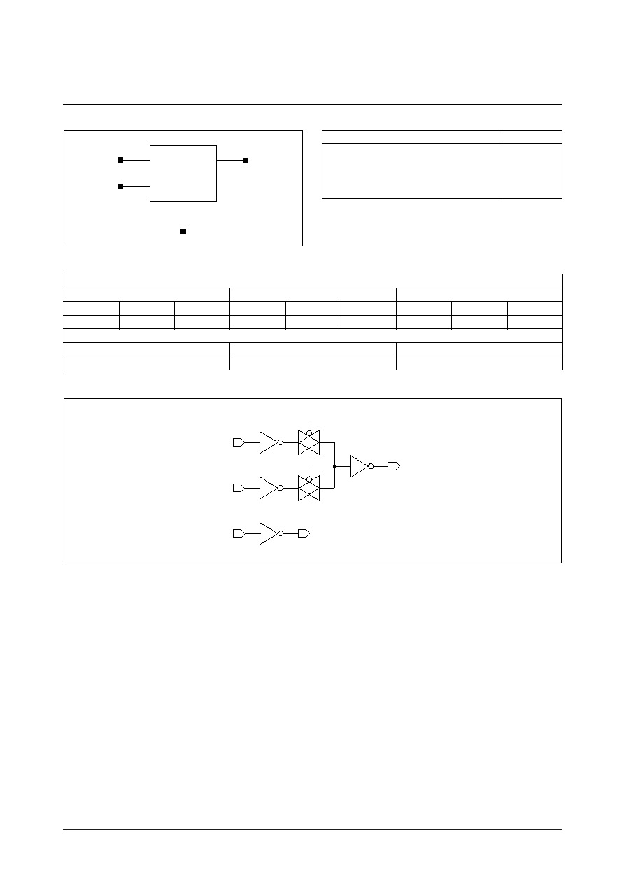
STDL130
3-330
Samsung ASIC
MX2_LP/MX2D2_LP/MX2D4_LP
2 > 1 Non-Inverting MUX with 1X/2X/4X Drive
Logic Symbol
Cell Data
Schematic Diagram
Input Load (SL)
MX2_LP
MX2D2_LP
MX2D4_LP
D0
D1
S
D0
D1
S
D0
D1
S
1.0
1.0
1.8
1.0
1.0
1.8
1.1
1.0
1.8
Gate Count
MX2_LP
MX2D2_LP
MX2D4_LP
3.33
3.67
4.67
D0
D1
Y
S
S
SB
Y
SB
S
S
D0
D1
Truth Table
D0
D1
S
Y
0
x
0
0
1
x
0
1
x
0
1
0
x
1
1
1

Samsung ASIC
3-331
STDL130
MX2_LP/MX2D2_LP/MX2D4_LP
2 > 1 Non-Inverting MUX with 1X/2X/4X Drive
Switching Characteristics
(Typical process, 25
∞
C, 1.8V, t
R
/t
F
= 0.22ns, SL: Standard Load)
MX2_LP
MX2D2_LP
Path
Parameter
Delay [ns]
SL = 2
Delay Equations [ns]
Group1*
Group2*
Group3*
D0 to Y
tR
0.114
0.059 + 0.027*SL
0.054 + 0.029*SL
0.049 + 0.030*SL
tF
0.112
0.069 + 0.022*SL
0.073 + 0.021*SL
0.073 + 0.021*SL
tPLH
0.219
0.187 + 0.016*SL
0.193 + 0.015*SL
0.196 + 0.014*SL
tPHL
0.267
0.231 + 0.018*SL
0.245 + 0.015*SL
0.257 + 0.013*SL
D1 to Y
tR
0.114
0.058 + 0.028*SL
0.053 + 0.029*SL
0.048 + 0.029*SL
tF
0.113
0.070 + 0.022*SL
0.072 + 0.021*SL
0.074 + 0.021*SL
tPLH
0.216
0.183 + 0.016*SL
0.190 + 0.014*SL
0.192 + 0.014*SL
tPHL
0.269
0.233 + 0.018*SL
0.247 + 0.015*SL
0.259 + 0.013*SL
S to Y
tR
0.114
0.060 + 0.027*SL
0.054 + 0.029*SL
0.049 + 0.029*SL
tF
0.111
0.067 + 0.022*SL
0.073 + 0.021*SL
0.073 + 0.021*SL
tPLH
0.244
0.211 + 0.016*SL
0.219 + 0.015*SL
0.221 + 0.014*SL
tPHL
0.240
0.204 + 0.018*SL
0.218 + 0.014*SL
0.229 + 0.013*SL
*Group1 : SL < 4, *Group2 : 4 SL
<
<
=
= 7, *Group3 : 7 < SL
Path
Parameter
Delay [ns]
SL = 2
Delay Equations [ns]
Group1*
Group2*
Group3*
D0 to Y
tR
0.088
0.060 + 0.014*SL
0.059 + 0.014*SL
0.053 + 0.015*SL
tF
0.096
0.070 + 0.013*SL
0.079 + 0.011*SL
0.084 + 0.010*SL
tPLH
0.219
0.198 + 0.010*SL
0.208 + 0.008*SL
0.217 + 0.007*SL
tPHL
0.272
0.248 + 0.012*SL
0.262 + 0.009*SL
0.282 + 0.007*SL
D1 to Y
tR
0.087
0.060 + 0.014*SL
0.058 + 0.014*SL
0.052 + 0.015*SL
tF
0.096
0.070 + 0.013*SL
0.078 + 0.011*SL
0.085 + 0.010*SL
tPLH
0.216
0.195 + 0.010*SL
0.204 + 0.008*SL
0.214 + 0.007*SL
tPHL
0.275
0.250 + 0.012*SL
0.264 + 0.009*SL
0.285 + 0.007*SL
S to Y
tR
0.087
0.057 + 0.015*SL
0.062 + 0.014*SL
0.054 + 0.015*SL
tF
0.095
0.070 + 0.013*SL
0.076 + 0.011*SL
0.085 + 0.010*SL
tPLH
0.241
0.220 + 0.010*SL
0.230 + 0.008*SL
0.240 + 0.007*SL
tPHL
0.248
0.224 + 0.012*SL
0.238 + 0.009*SL
0.258 + 0.007*SL
*Group1 : SL < 4, *Group2 : 4 SL
<
<
=
= 11, *Group3 : 11 < SL

STDL130
3-332
Samsung ASIC
MX2_LP/MX2D2_LP/MX2D4_LP
2 > 1 Non-Inverting MUX with 1X/2X/4X Drive
Switching Characteristics
(Typical process, 25
∞
C, 1.8V, t
R
/t
F
= 0.22ns, SL: Standard Load)
MX2D4_LP
Path
Parameter
Delay [ns]
SL = 2
Delay Equations [ns]
Group1*
Group2*
Group3*
D0 to Y
tR
0.090
0.073 + 0.009*SL
0.078 + 0.007*SL
0.078 + 0.007*SL
tF
0.102
0.087 + 0.008*SL
0.095 + 0.006*SL
0.110 + 0.005*SL
tPLH
0.255
0.241 + 0.007*SL
0.249 + 0.005*SL
0.269 + 0.004*SL
tPHL
0.300
0.285 + 0.008*SL
0.295 + 0.005*SL
0.325 + 0.004*SL
D1 to Y
tR
0.089
0.072 + 0.009*SL
0.078 + 0.007*SL
0.078 + 0.007*SL
tF
0.102
0.087 + 0.008*SL
0.094 + 0.006*SL
0.110 + 0.005*SL
tPLH
0.255
0.241 + 0.007*SL
0.249 + 0.005*SL
0.269 + 0.004*SL
tPHL
0.304
0.289 + 0.008*SL
0.299 + 0.005*SL
0.329 + 0.004*SL
S to Y
tR
0.091
0.074 + 0.008*SL
0.079 + 0.007*SL
0.079 + 0.007*SL
tF
0.102
0.086 + 0.008*SL
0.095 + 0.006*SL
0.110 + 0.005*SL
tPLH
0.270
0.256 + 0.007*SL
0.265 + 0.005*SL
0.284 + 0.004*SL
tPHL
0.287
0.271 + 0.008*SL
0.282 + 0.005*SL
0.311 + 0.004*SL
*Group1 : SL < 4, *Group2 : 4 SL
<
<
=
= 19, *Group3 : 19 < SL
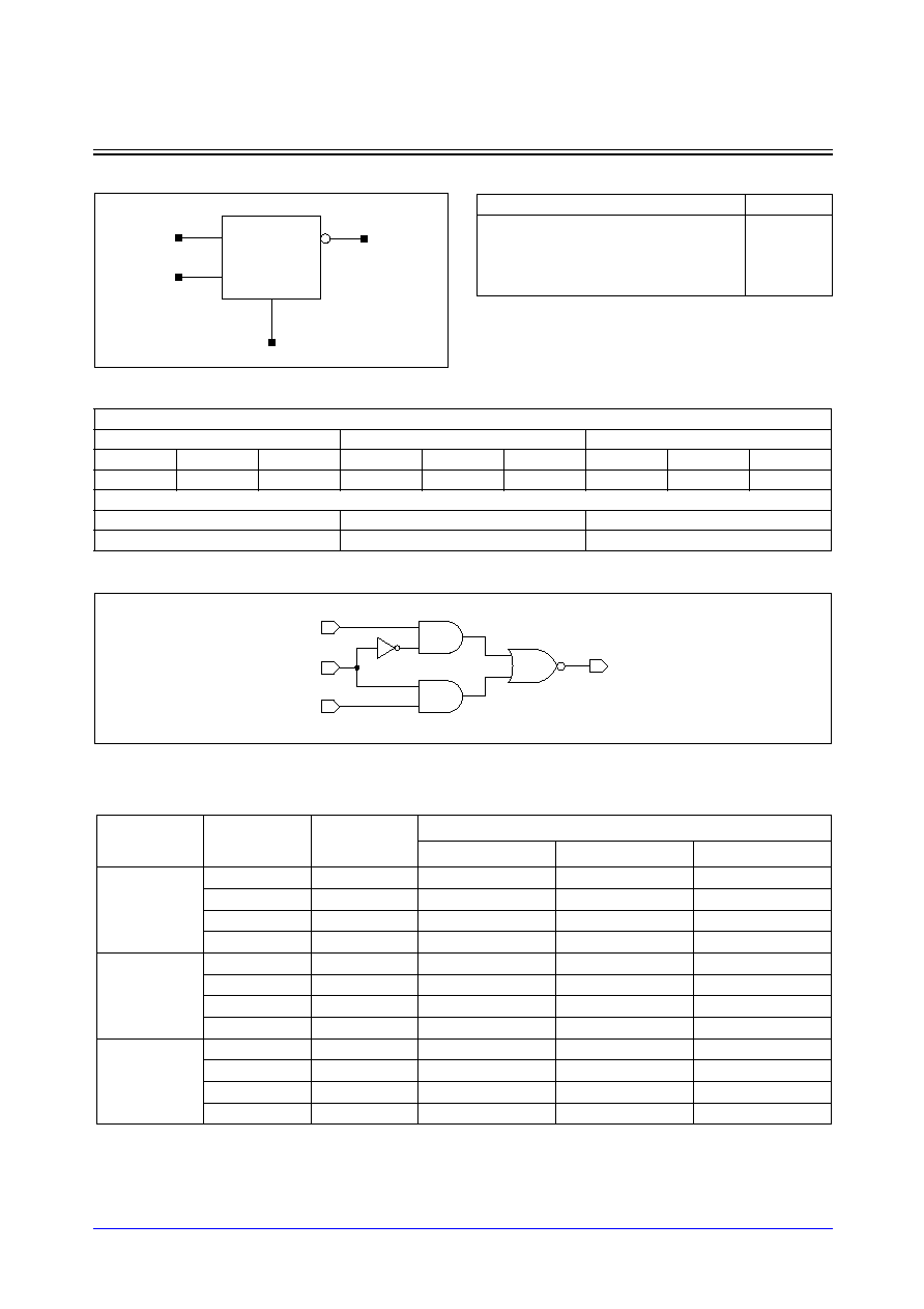
Samsung ASIC
3-333
STDL130
MX2I_LP/MX2ID2_LP/MX2ID4_LP
2 > 1 Inverting MUX with 1X/2X/4X Drive
Logic Symbol
Cell Data
Schematic Diagram
Switching Characteristics
(Typical process, 25
∞
C, 1.8V, t
R
/t
F
= 0.22ns, SL: Standard Load)
MX2I_LP
Input Load (SL)
MX2I_LP
MX2ID2_LP
MX2ID4_LP
D0
D1
S
D0
D1
S
D0
D1
S
1.0
1.0
1.9
1.9
1.9
2.9
1.0
1.0
1.8
Gate Count
MX2I_LP
MX2ID2_LP
MX2ID4_LP
2.33
3.67
4.33
D0
D1
YN
S
YN
D0
S
D1
Path
Parameter
Delay [ns]
SL = 2
Delay Equations [ns]
Group1*
Group2*
Group3*
D0 to YN
tR
0.265
0.148 + 0.058*SL
0.139 + 0.061*SL
0.128 + 0.062*SL
tF
0.178
0.108 + 0.035*SL
0.098 + 0.037*SL
0.087 + 0.039*SL
tPLH
0.177
0.116 + 0.030*SL
0.116 + 0.030*SL
0.117 + 0.030*SL
tPHL
0.132
0.088 + 0.022*SL
0.093 + 0.021*SL
0.093 + 0.021*SL
D1 to YN
tR
0.260
0.139 + 0.061*SL
0.135 + 0.062*SL
0.132 + 0.062*SL
tF
0.225
0.151 + 0.037*SL
0.147 + 0.038*SL
0.139 + 0.039*SL
tPLH
0.233
0.172 + 0.031*SL
0.173 + 0.030*SL
0.174 + 0.030*SL
tPHL
0.186
0.141 + 0.022*SL
0.144 + 0.022*SL
0.148 + 0.021*SL
S to YN
tR
0.259
0.138 + 0.060*SL
0.132 + 0.062*SL
0.130 + 0.062*SL
tF
0.203
0.126 + 0.038*SL
0.121 + 0.040*SL
0.119 + 0.040*SL
tPLH
0.218
0.158 + 0.030*SL
0.158 + 0.030*SL
0.159 + 0.030*SL
tPHL
0.207
0.164 + 0.021*SL
0.167 + 0.021*SL
0.167 + 0.021*SL
*Group1 : SL < 4, *Group2 : 4 SL
<
<
=
= 7, *Group3 : 7 < SL
Truth Table
D0
D1
S
YN
0
x
0
1
1
x
0
0
x
0
1
1
x
1
1
0

STDL130
3-334
Samsung ASIC
MX2I_LP/MX2ID2_LP/MX2ID4_LP
2 > 1 Inverting MUX with 1X/2X/4X Drive
Switching Characteristics
(Typical process, 25
∞
C, 1.8V, t
R
/t
F
= 0.22ns, SL: Standard Load)
MX2ID2_LP
MX2ID4_LP
Path
Parameter
Delay [ns]
SL = 2
Delay Equations [ns]
Group1*
Group2*
Group3*
D0 to YN
tR
0.213
0.156 + 0.029*SL
0.150 + 0.030*SL
0.139 + 0.031*SL
tF
0.147
0.114 + 0.017*SL
0.108 + 0.018*SL
0.096 + 0.019*SL
tPLH
0.152
0.122 + 0.015*SL
0.121 + 0.015*SL
0.122 + 0.015*SL
tPHL
0.113
0.089 + 0.012*SL
0.095 + 0.011*SL
0.096 + 0.010*SL
D1 to YN
tR
0.204
0.144 + 0.030*SL
0.142 + 0.031*SL
0.138 + 0.031*SL
tF
0.187
0.152 + 0.018*SL
0.147 + 0.019*SL
0.140 + 0.019*SL
tPLH
0.199
0.168 + 0.015*SL
0.169 + 0.015*SL
0.170 + 0.015*SL
tPHL
0.161
0.139 + 0.011*SL
0.141 + 0.011*SL
0.144 + 0.011*SL
S to YN
tR
0.200
0.139 + 0.030*SL
0.136 + 0.031*SL
0.135 + 0.031*SL
tF
0.160
0.124 + 0.018*SL
0.120 + 0.019*SL
0.113 + 0.020*SL
tPLH
0.200
0.169 + 0.015*SL
0.169 + 0.015*SL
0.171 + 0.015*SL
tPHL
0.217
0.195 + 0.011*SL
0.198 + 0.011*SL
0.200 + 0.010*SL
*Group1 : SL < 4, *Group2 : 4 SL
<
<
=
= 11, *Group3 : 11 < SL
Path
Parameter
Delay [ns]
SL = 2
Delay Equations [ns]
Group1*
Group2*
Group3*
D0 to YN
tR
0.071
0.056 + 0.008*SL
0.059 + 0.007*SL
0.047 + 0.007*SL
tF
0.060
0.047 + 0.006*SL
0.053 + 0.005*SL
0.051 + 0.005*SL
tPLH
0.343
0.332 + 0.006*SL
0.339 + 0.004*SL
0.348 + 0.004*SL
tPHL
0.277
0.267 + 0.005*SL
0.273 + 0.004*SL
0.287 + 0.003*SL
D1 to YN
tR
0.072
0.058 + 0.007*SL
0.058 + 0.007*SL
0.048 + 0.007*SL
tF
0.061
0.050 + 0.006*SL
0.053 + 0.005*SL
0.052 + 0.005*SL
tPLH
0.398
0.387 + 0.006*SL
0.393 + 0.004*SL
0.402 + 0.004*SL
tPHL
0.319
0.308 + 0.005*SL
0.315 + 0.004*SL
0.329 + 0.003*SL
S to YN
tR
0.072
0.058 + 0.007*SL
0.059 + 0.007*SL
0.047 + 0.007*SL
tF
0.061
0.048 + 0.006*SL
0.053 + 0.005*SL
0.052 + 0.005*SL
tPLH
0.382
0.371 + 0.006*SL
0.378 + 0.004*SL
0.387 + 0.004*SL
tPHL
0.339
0.329 + 0.005*SL
0.335 + 0.004*SL
0.349 + 0.003*SL
*Group1 : SL < 4, *Group2 : 4 SL
<
<
=
= 19, *Group3 : 19 < SL
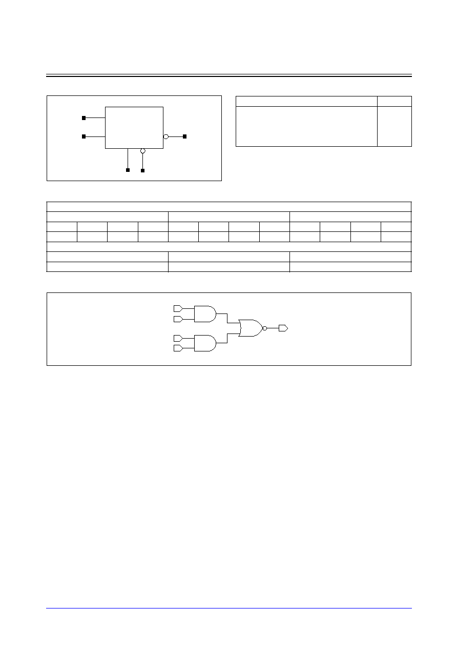
Samsung ASIC
3-335
STDL130
MX2IA_LP/MX2ID2A_LP/MX2ID4A_LP
2 > 1 Inverting MUX with Separate S and SN Inputs, 1X/2X/4X Drive
Logic Symbol
Cell Data
Schematic Diagram
Input Load (SL)
MX2IA_LP
MX2ID2A_LP
MX2ID4A_LP
D0
D1
S
SN
D0
D1
S
SN
D0
D1
S
SN
1.0
1.0
1.0
1.0
1.9
1.9
2.1
2.0
1.0
1.1
1.0
1.0
Gate Count
MX2IA_LP
MX2ID2A_LP
MX2ID4A_LP
2.00
3.00
3.67
YN
D0
D1
S
SN
YN
D0
SN
D1
S
Truth Table
D0
D1
S
SN
YN
0
x
0
1
1
1
x
0
1
0
x
0
1
0
1
x
1
1
0
0
STDL130
3-336
Samsung ASIC
MX2IA_LP/MX2ID2A_LP/MX2ID4A_LP
2 > 1 Inverting MUX with Separate S and SN Inputs, 1X/2X/4X Drive
Switching Characteristics
(Typical process, 25
∞
C, 1.8V, t
R
/t
F
= 0.22ns, SL: Standard Load)
MX2IA_LP
MX2ID2A_LP
Path
Parameter
Delay [ns]
SL = 2
Delay Equations [ns]
Group1*
Group2*
Group3*
D0 to YN
tR
0.275
0.160 + 0.057*SL
0.151 + 0.060*SL
0.141 + 0.061*SL
tF
0.184
0.114 + 0.035*SL
0.103 + 0.038*SL
0.094 + 0.039*SL
tPLH
0.180
0.121 + 0.030*SL
0.120 + 0.030*SL
0.121 + 0.030*SL
tPHL
0.138
0.094 + 0.022*SL
0.097 + 0.021*SL
0.098 + 0.021*SL
D1 to YN
tR
0.271
0.152 + 0.059*SL
0.147 + 0.061*SL
0.145 + 0.061*SL
tF
0.228
0.153 + 0.038*SL
0.150 + 0.038*SL
0.144 + 0.039*SL
tPLH
0.240
0.180 + 0.030*SL
0.181 + 0.030*SL
0.182 + 0.030*SL
tPHL
0.195
0.150 + 0.022*SL
0.154 + 0.022*SL
0.157 + 0.021*SL
S to YN
tR
0.284
0.164 + 0.060*SL
0.161 + 0.061*SL
0.158 + 0.061*SL
tF
0.225
0.148 + 0.038*SL
0.146 + 0.039*SL
0.143 + 0.039*SL
tPLH
0.252
0.193 + 0.030*SL
0.194 + 0.030*SL
0.194 + 0.030*SL
tPHL
0.191
0.146 + 0.022*SL
0.149 + 0.022*SL
0.153 + 0.021*SL
SN to YN
tR
0.287
0.172 + 0.058*SL
0.163 + 0.060*SL
0.154 + 0.061*SL
tF
0.176
0.103 + 0.037*SL
0.097 + 0.038*SL
0.092 + 0.039*SL
tPLH
0.192
0.132 + 0.030*SL
0.132 + 0.030*SL
0.133 + 0.030*SL
tPHL
0.133
0.089 + 0.022*SL
0.093 + 0.021*SL
0.093 + 0.021*SL
*Group1 : SL < 4, *Group2 : 4 SL
<
<
=
= 7, *Group3 : 7 < SL
Path
Parameter
Delay [ns]
SL = 2
Delay Equations [ns]
Group1*
Group2*
Group3*
D0 to YN
tR
0.202
0.145 + 0.029*SL
0.140 + 0.030*SL
0.127 + 0.031*SL
tF
0.139
0.106 + 0.017*SL
0.100 + 0.018*SL
0.088 + 0.019*SL
tPLH
0.145
0.115 + 0.015*SL
0.114 + 0.015*SL
0.115 + 0.015*SL
tPHL
0.107
0.082 + 0.013*SL
0.090 + 0.011*SL
0.091 + 0.010*SL
D1 to YN
tR
0.193
0.133 + 0.030*SL
0.130 + 0.031*SL
0.126 + 0.031*SL
tF
0.172
0.135 + 0.019*SL
0.134 + 0.019*SL
0.127 + 0.019*SL
tPLH
0.195
0.164 + 0.015*SL
0.165 + 0.015*SL
0.166 + 0.015*SL
tPHL
0.160
0.137 + 0.012*SL
0.139 + 0.011*SL
0.143 + 0.011*SL
S to YN
tR
0.206
0.147 + 0.030*SL
0.143 + 0.031*SL
0.140 + 0.031*SL
tF
0.168
0.130 + 0.019*SL
0.129 + 0.019*SL
0.125 + 0.020*SL
tPLH
0.208
0.177 + 0.015*SL
0.178 + 0.015*SL
0.179 + 0.015*SL
tPHL
0.155
0.132 + 0.012*SL
0.134 + 0.011*SL
0.138 + 0.011*SL
SN to YN
tR
0.214
0.157 + 0.029*SL
0.151 + 0.030*SL
0.141 + 0.031*SL
tF
0.131
0.094 + 0.018*SL
0.093 + 0.018*SL
0.082 + 0.019*SL
tPLH
0.157
0.127 + 0.015*SL
0.126 + 0.015*SL
0.127 + 0.015*SL
tPHL
0.102
0.078 + 0.012*SL
0.084 + 0.011*SL
0.087 + 0.010*SL
*Group1 : SL < 4, *Group2 : 4 SL
<
<
=
= 11, *Group3 : 11 < SL
Samsung ASIC
3-337
STDL130
MX2IA_LP/MX2ID2A_LP/MX2ID4A_LP
2 > 1 Inverting MUX with Separate S and SN Inputs, 1X/2X/4X Drive
Switching Characteristics
(Typical process, 25
∞
C, 1.8V, t
R
/t
F
= 0.22ns, SL: Standard Load)
MX2ID4A_LP
Path
Parameter
Delay [ns]
SL = 2
Delay Equations [ns]
Group1*
Group2*
Group3*
D0 to YN
tR
0.071
0.057 + 0.007*SL
0.058 + 0.007*SL
0.048 + 0.007*SL
tF
0.061
0.048 + 0.006*SL
0.053 + 0.005*SL
0.051 + 0.005*SL
tPLH
0.338
0.326 + 0.006*SL
0.333 + 0.004*SL
0.342 + 0.004*SL
tPHL
0.274
0.263 + 0.005*SL
0.269 + 0.004*SL
0.283 + 0.003*SL
D1 to YN
tR
0.071
0.058 + 0.007*SL
0.057 + 0.007*SL
0.048 + 0.007*SL
tF
0.061
0.048 + 0.007*SL
0.053 + 0.005*SL
0.051 + 0.005*SL
tPLH
0.393
0.382 + 0.006*SL
0.388 + 0.004*SL
0.397 + 0.004*SL
tPHL
0.312
0.301 + 0.005*SL
0.308 + 0.004*SL
0.322 + 0.003*SL
S to YN
tR
0.072
0.059 + 0.007*SL
0.058 + 0.007*SL
0.047 + 0.007*SL
tF
0.062
0.050 + 0.006*SL
0.054 + 0.005*SL
0.051 + 0.005*SL
tPLH
0.409
0.398 + 0.006*SL
0.404 + 0.004*SL
0.413 + 0.004*SL
tPHL
0.308
0.297 + 0.005*SL
0.303 + 0.004*SL
0.317 + 0.003*SL
SN to YN
tR
0.072
0.059 + 0.007*SL
0.058 + 0.007*SL
0.048 + 0.007*SL
tF
0.061
0.050 + 0.006*SL
0.051 + 0.005*SL
0.051 + 0.005*SL
tPLH
0.359
0.347 + 0.006*SL
0.354 + 0.004*SL
0.363 + 0.004*SL
tPHL
0.269
0.258 + 0.005*SL
0.265 + 0.004*SL
0.279 + 0.003*SL
*Group1 : SL < 4, *Group2 : 4 SL
<
<
=
= 19, *Group3 : 19 < SL
STDL130
3-338
Samsung ASIC
MX4_LP/MX4D2_LP/MX4D4_LP
4 > 1 Non-Inverting MUX with 1X/2X/4X Drive
Logic Symbol
Cell Data
Schematic Diagram
Input Load (SL)
MX4_LP
MX4D2_LP
MX4D4_LP
D0
D1
D2
D3
S0
S1
D0
D1
D2
D3
S0
S1
D0
D1
D2
D3
S0
S1
1.0
1.0
1.0
1.0
2.6
1.6
1.0
1.0
1.0
1.0
2.7
1.6
1.0
1.0
1.0
1.0
2.7
1.6
Gate Count
MX4_LP
MX4D2_LP
MX4D4_LP
7.67
8.00
8.67
Y
D0
D1
D2
D3
S0
S1
S0B
S0
S0
S1B
S1
S1
D0
D1
D2
D3
Y
S0
S0
S0B
S0
S0B
S1
S1B
S1B
S1
Truth Table
S0
S1
Y
0
0
D0
1
0
D1
0
1
D2
1
1
D3

Samsung ASIC
3-339
STDL130
MX4_LP/MX4D2_LP/MX4D4_LP
4 > 1 Non-Inverting MUX with 1X/2X/4X Drive
Switching Characteristics
(Typical process, 25
∞
C, 1.8V, t
R
/t
F
= 0.22ns, SL: Standard Load)
MX4_LP
Path
Parameter
Delay [ns]
SL = 2
Delay Equations [ns]
Group1*
Group2*
Group3*
D0 to Y
tR
0.135
0.077 + 0.029*SL
0.079 + 0.028*SL
0.076 + 0.029*SL
tF
0.145
0.100 + 0.023*SL
0.109 + 0.020*SL
0.113 + 0.020*SL
tPLH
0.335
0.296 + 0.019*SL
0.309 + 0.016*SL
0.319 + 0.015*SL
tPHL
0.367
0.324 + 0.021*SL
0.343 + 0.017*SL
0.362 + 0.014*SL
D1 to Y
tR
0.135
0.078 + 0.029*SL
0.079 + 0.028*SL
0.076 + 0.029*SL
tF
0.145
0.100 + 0.023*SL
0.109 + 0.020*SL
0.112 + 0.020*SL
tPLH
0.331
0.293 + 0.019*SL
0.306 + 0.016*SL
0.315 + 0.015*SL
tPHL
0.366
0.324 + 0.021*SL
0.343 + 0.016*SL
0.361 + 0.014*SL
D2 to Y
tR
0.135
0.077 + 0.029*SL
0.080 + 0.028*SL
0.075 + 0.029*SL
tF
0.144
0.099 + 0.023*SL
0.108 + 0.020*SL
0.111 + 0.020*SL
tPLH
0.328
0.290 + 0.019*SL
0.303 + 0.016*SL
0.312 + 0.015*SL
tPHL
0.362
0.320 + 0.021*SL
0.339 + 0.016*SL
0.357 + 0.014*SL
D3 to Y
tR
0.135
0.077 + 0.029*SL
0.080 + 0.028*SL
0.075 + 0.029*SL
tF
0.144
0.099 + 0.023*SL
0.108 + 0.020*SL
0.110 + 0.020*SL
tPLH
0.326
0.288 + 0.019*SL
0.301 + 0.016*SL
0.310 + 0.015*SL
tPHL
0.363
0.321 + 0.021*SL
0.340 + 0.016*SL
0.358 + 0.014*SL
S0 to Y
tR
0.135
0.077 + 0.029*SL
0.078 + 0.029*SL
0.076 + 0.029*SL
tF
0.144
0.099 + 0.023*SL
0.108 + 0.021*SL
0.112 + 0.020*SL
tPLH
0.357
0.319 + 0.019*SL
0.332 + 0.016*SL
0.342 + 0.015*SL
tPHL
0.372
0.329 + 0.021*SL
0.348 + 0.017*SL
0.366 + 0.014*SL
S1 to Y
tR
0.131
0.073 + 0.029*SL
0.076 + 0.029*SL
0.074 + 0.029*SL
tF
0.131
0.084 + 0.024*SL
0.093 + 0.021*SL
0.102 + 0.020*SL
tPLH
0.256
0.218 + 0.019*SL
0.231 + 0.016*SL
0.240 + 0.015*SL
tPHL
0.257
0.216 + 0.020*SL
0.233 + 0.016*SL
0.250 + 0.014*SL
*Group1 : SL < 4, *Group2 : 4 SL
<
<
=
= 7, *Group3 : 7 < SL

STDL130
3-340
Samsung ASIC
MX4_LP/MX4D2_LP/MX4D4_LP
4 > 1 Non-Inverting MUX with 1X/2X/4X Drive
Switching Characteristics
(Typical process, 25
∞
C, 1.8V, t
R
/t
F
= 0.22ns, SL: Standard Load)
MX4D2_LP
Path
Parameter
Delay [ns]
SL = 2
Delay Equations [ns]
Group1*
Group2*
Group3*
D0 to Y
tR
0.110
0.077 + 0.017*SL
0.085 + 0.015*SL
0.089 + 0.014*SL
tF
0.135
0.106 + 0.015*SL
0.120 + 0.011*SL
0.132 + 0.010*SL
tPLH
0.347
0.321 + 0.013*SL
0.334 + 0.010*SL
0.354 + 0.008*SL
tPHL
0.387
0.358 + 0.015*SL
0.375 + 0.010*SL
0.404 + 0.008*SL
D1 to Y
tR
0.110
0.077 + 0.017*SL
0.086 + 0.014*SL
0.088 + 0.014*SL
tF
0.135
0.106 + 0.015*SL
0.120 + 0.011*SL
0.132 + 0.010*SL
tPLH
0.344
0.319 + 0.013*SL
0.332 + 0.010*SL
0.351 + 0.008*SL
tPHL
0.387
0.358 + 0.015*SL
0.375 + 0.010*SL
0.404 + 0.008*SL
D2 to Y
tR
0.109
0.076 + 0.017*SL
0.084 + 0.015*SL
0.087 + 0.014*SL
tF
0.134
0.106 + 0.014*SL
0.117 + 0.011*SL
0.131 + 0.010*SL
tPLH
0.339
0.314 + 0.013*SL
0.327 + 0.009*SL
0.346 + 0.008*SL
tPHL
0.382
0.353 + 0.015*SL
0.370 + 0.010*SL
0.399 + 0.008*SL
D3 to Y
tR
0.109
0.077 + 0.016*SL
0.084 + 0.015*SL
0.087 + 0.014*SL
tF
0.134
0.106 + 0.014*SL
0.117 + 0.011*SL
0.131 + 0.010*SL
tPLH
0.338
0.312 + 0.013*SL
0.325 + 0.009*SL
0.345 + 0.008*SL
tPHL
0.383
0.354 + 0.015*SL
0.371 + 0.010*SL
0.400 + 0.008*SL
S0 to Y
tR
0.111
0.079 + 0.016*SL
0.085 + 0.015*SL
0.089 + 0.014*SL
tF
0.135
0.106 + 0.014*SL
0.119 + 0.011*SL
0.131 + 0.010*SL
tPLH
0.369
0.344 + 0.013*SL
0.357 + 0.010*SL
0.376 + 0.008*SL
tPHL
0.396
0.366 + 0.015*SL
0.384 + 0.010*SL
0.413 + 0.008*SL
S1 to Y
tR
0.109
0.077 + 0.016*SL
0.083 + 0.015*SL
0.087 + 0.014*SL
tF
0.126
0.097 + 0.014*SL
0.109 + 0.012*SL
0.124 + 0.010*SL
tPLH
0.265
0.240 + 0.013*SL
0.253 + 0.010*SL
0.272 + 0.008*SL
tPHL
0.282
0.253 + 0.014*SL
0.270 + 0.010*SL
0.298 + 0.008*SL
*Group1 : SL < 4, *Group2 : 4 SL
<
<
=
= 11, *Group3 : 11 < SL

Samsung ASIC
3-341
STDL130
MX4_LP/MX4D2_LP/MX4D4_LP
4 > 1 Non-Inverting MUX with 1X/2X/4X Drive
Switching Characteristics
(Typical process, 25
∞
C, 1.8V, t
R
/t
F
= 0.22ns, SL: Standard Load)
MX4D4_LP
Path
Parameter
Delay [ns]
SL = 2
Delay Equations [ns]
Group1*
Group2*
Group3*
D0 to Y
tR
0.118
0.098 + 0.010*SL
0.107 + 0.008*SL
0.122 + 0.007*SL
tF
0.162
0.144 + 0.009*SL
0.153 + 0.007*SL
0.180 + 0.005*SL
tPLH
0.407
0.390 + 0.008*SL
0.400 + 0.006*SL
0.431 + 0.004*SL
tPHL
0.468
0.449 + 0.010*SL
0.461 + 0.007*SL
0.503 + 0.005*SL
D1 to Y
tR
0.118
0.098 + 0.010*SL
0.106 + 0.008*SL
0.122 + 0.007*SL
tF
0.162
0.144 + 0.009*SL
0.153 + 0.007*SL
0.180 + 0.005*SL
tPLH
0.404
0.388 + 0.008*SL
0.398 + 0.006*SL
0.429 + 0.004*SL
tPHL
0.469
0.449 + 0.010*SL
0.461 + 0.007*SL
0.503 + 0.005*SL
D2 to Y
tR
0.117
0.097 + 0.010*SL
0.105 + 0.008*SL
0.122 + 0.007*SL
tF
0.160
0.141 + 0.009*SL
0.152 + 0.007*SL
0.178 + 0.005*SL
tPLH
0.397
0.381 + 0.008*SL
0.391 + 0.006*SL
0.421 + 0.004*SL
tPHL
0.461
0.441 + 0.010*SL
0.453 + 0.007*SL
0.495 + 0.005*SL
D3 to Y
tR
0.117
0.098 + 0.010*SL
0.104 + 0.008*SL
0.122 + 0.007*SL
tF
0.160
0.141 + 0.009*SL
0.152 + 0.007*SL
0.178 + 0.005*SL
tPLH
0.396
0.379 + 0.008*SL
0.389 + 0.006*SL
0.420 + 0.004*SL
tPHL
0.461
0.442 + 0.010*SL
0.454 + 0.007*SL
0.496 + 0.005*SL
S0 to Y
tR
0.118
0.098 + 0.010*SL
0.106 + 0.008*SL
0.123 + 0.007*SL
tF
0.162
0.145 + 0.009*SL
0.153 + 0.007*SL
0.180 + 0.005*SL
tPLH
0.428
0.412 + 0.008*SL
0.422 + 0.006*SL
0.452 + 0.004*SL
tPHL
0.481
0.461 + 0.010*SL
0.474 + 0.007*SL
0.515 + 0.005*SL
S1 to Y
tR
0.118
0.098 + 0.010*SL
0.106 + 0.008*SL
0.121 + 0.007*SL
tF
0.158
0.140 + 0.009*SL
0.149 + 0.007*SL
0.175 + 0.005*SL
tPLH
0.320
0.303 + 0.008*SL
0.313 + 0.006*SL
0.344 + 0.004*SL
tPHL
0.373
0.353 + 0.010*SL
0.365 + 0.007*SL
0.408 + 0.005*SL
*Group1 : SL < 4, *Group2 : 4 SL
<
<
=
= 19, *Group3 : 19 < SL

STDL130
3-342
Samsung ASIC
INTEGRATED CLOCK-GATING CELLS
Cell ListCell List
Cell Name
Function Description
CGLN_LP
Negative Edge Triggered Clock-Gating with 1X Drive
CGLND2_LP
Negative Edge Triggered Clock-Gating with 2X Drive
CGLND4_LP
Negative Edge Triggered Clock-Gating with 4X Drive
CGLP_LP
Positive Edge Triggered Clock-Gating with 1X Drive
CGLPD2_LP
Positive Edge Triggered Clock-Gating with 2X Drive
CGLPD4_LP
Positive Edge Triggered Clock-Gating with 4X Drive
Samsung ASIC
3-343
STDL130
CGLN_LP/CGLND2_LP/CGLND4_LP
Negative Edge Triggered Clock-Gating with 1X/2X/4X Drive
Logic Symbol
Cell Data
Schematic Diagram
Input Load (SL)
CGLN_LP
CGLND2_LP
CGLND4_LP
EN
CK
TE
EN
CK
TE
EN
CK
TE
1.0
0.9
1.1
1.0
1.0
1.1
1.0
1.0
1.1
Gate Count
CGLN_LP
CGLND2_LP
CGLND4_LP
4.67
5.33
6.67
Truth Table
CK
EN
TE
GCK
0
0
1
1
x
0
x
1
0
1
x
x
1
TE
EN
CK
GCK
LD1Q
CL
CLB
CLB
CL
CK
CL
CLB
TE
EN
CLB
GCK

STDL130
3-344
Samsung ASIC
CGLN_LP/CGLND2_LP/CGLND4_LP
Negative Edge Triggered Clock-Gating with 1X/2X/4X Drive
Timing Requirements
(Typical process, 25
∞
C, 1.8V, Unit = ns)
Parameter
Symbol
Value (ns)
CGLN_LP
CGLND2_LP
CGLND4_LP
Input Setup Time (EN to CK)
t
SU
0.224
0.224
0.214
Input Hold Time (EN to CK)
t
HD
0.038
0.053
0.081
Pulse Width High (CK)
t
PWH
0.171
0.191
0.233
Input Setup Time (TE to CK)
t
SU
0.253
0.253
0.243
Input Hold Time (TE to CK)
t
HD
0.024
0.038
0.065
Samsung ASIC
3-345
STDL130
CGLN_LP/CGLND2_LP/CGLND4_LP
Negative Edge Triggered Clock-Gating with 1X/2X/4X Drive
Switching Characteristics
(Typical process, 25
∞
C, 1.8V, t
R
/t
F
= 0.22ns, SL: Standard Load)
CGLN_LP
CGLND2_LP
CGLND4_LP
Path
Parameter
Delay [ns]
SL = 2
Delay Equations [ns]
Group1*
Group2*
Group3*
CK to GCK
tR
0.127
0.070 + 0.028*SL
0.066 + 0.029*SL
0.060 + 0.030*SL
tF
0.122
0.066 + 0.028*SL
0.064 + 0.028*SL
0.059 + 0.029*SL
tPLH
0.223
0.190 + 0.017*SL
0.197 + 0.015*SL
0.200 + 0.014*SL
tPHL
0.216
0.181 + 0.018*SL
0.188 + 0.016*SL
0.191 + 0.016*SL
*Group1 : SL < 4, *Group2 : 4 SL
<
<
=
= 7, *Group3 : 7 < SL
Path
Parameter
Delay [ns]
SL = 2
Delay Equations [ns]
Group1*
Group2*
Group3*
CK to GCK
tR
0.103
0.076 + 0.014*SL
0.074 + 0.014*SL
0.068 + 0.015*SL
tF
0.095
0.065 + 0.015*SL
0.069 + 0.014*SL
0.065 + 0.014*SL
tPLH
0.225
0.205 + 0.010*SL
0.213 + 0.008*SL
0.221 + 0.007*SL
tPHL
0.217
0.197 + 0.010*SL
0.203 + 0.009*SL
0.212 + 0.008*SL
*Group1 : SL < 4, *Group2 : 4 SL
<
<
=
= 11, *Group3 : 11 < SL
Path
Parameter
Delay [ns]
SL = 2
Delay Equations [ns]
Group1*
Group2*
Group3*
CK to GCK
tR
0.105
0.091 + 0.007*SL
0.092 + 0.007*SL
0.089 + 0.007*SL
tF
0.095
0.079 + 0.008*SL
0.083 + 0.007*SL
0.082 + 0.007*SL
tPLH
0.258
0.246 + 0.006*SL
0.252 + 0.005*SL
0.269 + 0.004*SL
tPHL
0.248
0.235 + 0.006*SL
0.241 + 0.005*SL
0.256 + 0.004*SL
*Group1 : SL < 4, *Group2 : 4 SL
<
<
=
= 19, *Group3 : 19 < SL
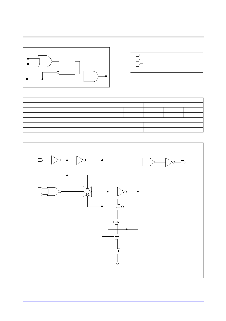
STDL130
3-346
Samsung ASIC
CGLP_LP/CGLPD2_LP/CGLPD4_LP
Positive Edge Triggered Clock-Gating with 1X/2X/4X Drive
Logic Symbol
Cell Data
Schematic Diagram
Input Load (SL)
CGLP_LP
CGLPD2_LP
CGLPD4_LP
EN
CK
TE
EN
CK
TE
EN
CK
TE
1.0
0.9
1.1
1.0
0.9
1.0
1.0
0.9
1.1
Gate Count
CGLP_LP
CGLPD2_LP
CGLPD4_LP
5.00
5.33
6.00
Truth Table
CK
EN
TE
GCK
0
0
0
1
x
1
x
1
1
0
x
x
0
CK
GCK
LD5Q
TE
EN
CK
GCK
EN
TE
Samsung ASIC
3-347
STDL130
CGLP_LP/CGLPD2_LP/CGLPD4_LP
Positive Edge Triggered Clock-Gating with 1X/2X/4X Drive
Timing Requirements
(Typical process, 25
∞
C, 1.8V, Unit = ns)
Parameter
Symbol
Value (ns)
CGLP_LP
CGLPD2_LP
CGLPD4_LP
Input Setup Time (EN to CK)
t
SU
0.166
0.166
0.166
Input Hold Time (EN to CK)
t
HD
0.010
0.010
0.010
Pulse Width Low (CK)
t
PWL
0.147
0.148
0.148
Input Setup Time (TE to CK)
t
SU
0.193
0.192
0.193
Input Hold Time (TE to CK)
t
HD
0.010
0.010
0.010

STDL130
3-348
Samsung ASIC
CGLP_LP/CGLPD2_LP/CGLPD4_LP
Positive Edge Triggered Clock-Gating with 1X/2X/4X Drive
Switching Characteristics
(Typical process, 25
∞
C, 1.8V, t
R
/t
F
= 0.22ns, SL: Standard Load)
CGLP_LP
CGLPD2_LP
CGLPD4_LP
Path
Parameter
Delay [ns]
SL = 2
Delay Equations [ns]
Group1*
Group2*
Group3*
CK to GCK
tR
0.104
0.047 + 0.029*SL
0.044 + 0.029*SL
0.041 + 0.030*SL
tF
0.081
0.039 + 0.021*SL
0.039 + 0.021*SL
0.035 + 0.022*SL
tPLH
0.298
0.268 + 0.015*SL
0.272 + 0.014*SL
0.273 + 0.014*SL
tPHL
0.318
0.291 + 0.014*SL
0.297 + 0.012*SL
0.299 + 0.012*SL
*Group1 : SL < 4, *Group2 : 4 SL
<
<
=
= 7, *Group3 : 7 < SL
Path
Parameter
Delay [ns]
SL = 2
Delay Equations [ns]
Group1*
Group2*
Group3*
CK to GCK
tR
0.078
0.049 + 0.014*SL
0.050 + 0.014*SL
0.042 + 0.015*SL
tF
0.063
0.043 + 0.010*SL
0.042 + 0.010*SL
0.041 + 0.011*SL
tPLH
0.304
0.285 + 0.009*SL
0.292 + 0.008*SL
0.298 + 0.007*SL
tPHL
0.323
0.306 + 0.009*SL
0.313 + 0.007*SL
0.322 + 0.006*SL
*Group1 : SL < 4, *Group2 : 4 SL
<
<
=
= 11, *Group3 : 11 < SL
Path
Parameter
Delay [ns]
SL = 2
Delay Equations [ns]
Group1*
Group2*
Group3*
CK to GCK
tR
0.079
0.064 + 0.008*SL
0.066 + 0.007*SL
0.060 + 0.007*SL
tF
0.066
0.055 + 0.006*SL
0.056 + 0.005*SL
0.057 + 0.005*SL
tPLH
0.335
0.322 + 0.006*SL
0.330 + 0.004*SL
0.345 + 0.004*SL
tPHL
0.352
0.340 + 0.006*SL
0.347 + 0.004*SL
0.364 + 0.003*SL
*Group1 : SL < 4, *Group2 : 4 SL
<
<
=
= 19, *Group3 : 19 < SL

4
Input/Output Cells

Contents
Overview...............................................................................................................................4-1
Summary Tables ...................................................................................................................4-2
Input Buffers .........................................................................................................................4-10
Output Buffers.......................................................................................................................4-23
Bi-Directional Buffers ............................................................................................................4-94
Input Clock Drivers ...............................................................................................................4-96
Oscillators .............................................................................................................................4-117
PCI Buffers ...........................................................................................................................4-141
Power Pads...........................................................................................................................4-147
Analog Interface....................................................................................................................4-149
Slot Cells ..............................................................................................................................4-181

INPUT/OUTPUT CELLS
OVERVIEW
Samsung ASIC
4-1
STDL130
OVERVIEW
This chapter describes the Input/Output cells (1.8V/2.5V/ 3.3V drive and 3.3V/5V-tolerant), power/ground
and ESD slot cells in the STDL130 library.
The switching characteristics of each cell follow the table of switching characteristics of the cell. The AC
characteristics of bi-directional buffers are not included in this data sheet. However, they are the same as
the component input and output buffers that make up the bi-directional buffer.
There are many possible combinations of input/output cells, therefore, the naming convention is adopted
to help efficiently identify the cell and its characteristics from its name (refer to the naming conventions
contained in "Summary Tables" section.)
The "Summary Tables" section shows the list of 1.8V/2.5V/3.3V drive and 3.3V/5V-tolerant I/O cells by
category (input, output, bi-directional, etc.). Moreover, each section begins with a table containing a brief
functional description of each cell in that section.
NOTES:
1.
As to analog IO cells in the library, the voltage level of the input/output signal is the same as the IO power supply
voltage level, no level shifter inside.
2.
When both A and B driving signals do not exist, SEC tolerant IO's pad voltage goes high state. However, those
3.3V tolerant and 5V tolerant input and bi-directional cells with 100k
pull-up resistor have NMOS pass transistor
like Figure 4.1. Therefore, pad voltage of 3.3V tolerant IO for 1.8V interface could be 1.0V instead of VDD, and pad
voltage of 5V tolerant IO for 3.3V interface could be 1.6V instead of VDD.
Figure 4-1.
PO
PI
VDD
PAD
B
A
TN
EN
A
SUMMARY TABLES
INPUT/OUTPUT CELLS
STDL130
4-2
Samsung ASIC
SUMMARY TABLES
Input Buffers
<Naming Convention of Input Buffers>
Output Buffers
Cell Type
Cell Name
Page
CMOS Level
PIC_LP/PICD_LP/PICU_LP
PTIC_LP/PTICD_LP/PTICU_LP
4-11
PMIC_LP/PMICD_LP/PMICU_LP
PHIC_LP/PHICD_LP/PHICU_LP
PHTIS_LP/PTISD_LP/PTISU_LP
CMOS Schmitt Trigger Level
PIS_LP/PISD_LP/PISU_LP
PTIS_LP/PTISD_LP/PTISU_LP
4-17
PMIS_LP/PMISD_LP/PMISU_LP
PHIS_LP/PHISD_LP/PHISU_LP
PHTIS_LP/PHTISD_LP/PMTISU_LP
Pvwlab_LP
v
w
a
b
None
1.8V interface
None
Normal
C
CMOS level
None
No resistor
M
2.5V interface
T
Tolerant
S
Schmitt trigger level
D
Pull-down resistor
H
3.3V interface
U
Pull-up resistor
Cell Type
Cell Name
Current Drive (mA)
Page
Normal
POBy_LP
1/2/4/8/12/16/20/24
4-24
POBySM_LP
4/8/12/16/20/24
POBySH_LP
12/16/20/24
PMOBy_LP
1/2/4/8/12/16/20/24
PMOBySM_LP
4/8/12/16/20/24
PMOBySH_LP
12/16/20/24
PHOBy_LP
1/2/4/8/12/16/20/24
PHOBySM_LP
4/8/12/16/20/24
PHOBySH_LP
12/16/20/24
INPUT/OUTPUT CELLS
SUMMARY TABLES
Samsung ASIC
4-3
STDL130
<Naming Convention of Output Buffers>
Open Drain
PODy_LP
1/2/4/8/12/16/20/24
4-40
PODySM_LP
4/8/12/16/20/24
PODySH_LP
12/16/20/24
PMODy_LP
1/2/4/8/12/16/20/24
PMODySM_LP
4/8/12/16/20/24
PMODySH_LP
12/16/20/24
PHODy_LP
1/2/4/8/12/16/20/24
PHODySM_LP
4/8/12/16/20/24
PHODySH_LP
12/16/20/24
PTODy_LP
1/2/4/6
PTODySM_LP
4/6
PHTODy_LP
1/2/4/6
PHTODySM_LP
4/6
Tri-State
POTy_LP
1/2/4/8/12/16/20/24
4-60
POTySM_LP
4/8/12/16/20/24
POTySH_LP
12/16/20/24
PMOTy_LP
1/2/4/8/12/16/20/24
PMOTySM_LP
4/8/12/16/20/24
PMOTySH_LP
12/16/20/24
PHOTy_LP
1/2/4/8/12/16/20/24
PHOTySM_LP
4/8/12/16/20/24
PHOTySH_LP
12/16/20/24
PTOTy_LP
1/2/4/6
PTOTySM_LP
4/6
PHTOTy_LP
1/2/4/6
PHTOTySM_LP
4/6
P v O x y z_LP: Normal Output Buffer
v
y
None
1.8V interface
1
1mA drive
M
2.5V interface
2
2mA drive
H
3.3V interface
4
4mA drive
x
8
8mA drive
B
Normal buffer
12
12mA drive
D
Open drain buffer
16
16mA drive
T
Tri-state buffer
20
20mA drive
z
24
24mA drive
Cell Type
Cell Name
Current Drive (mA)
Page
SUMMARY TABLES
INPUT/OUTPUT CELLS
STDL130
4-4
Samsung ASIC
Bi-Directional Buffers
None
No slew-rate control
SM
Medium slew-rate control
SH
High slew-rate control
P v T O x y z_LP: Tolerant Output Buffer
v
y
None
1.8V interface
1
1mA drive
M
2.5V interface
2
2mA drive
H
3.3V interface
4
4mA drive
x
6
6mA drive
D
Open drain buffer
T
Tri-state buffer
z
None
No slew-rate control
SM
Medium slew-rate control
Cell Type
Cell Name
Page
Open Drain
PBaDyz_LP/PBaUDyz_LP
PTBaDyz_LP/PTBaUDyz_LP
4-95
PMBaDyz_LP/PMBaUDyz_LP
PHBaDyz_LP/PHBaUDyz_LP
PHTBaDyz_LP/PHTBaUDyz_LP
Tri-State
PBaTyz_LP/PBaDTyz_LP/PBaUTyz_LP
PTBaTyz_LP/PTBaDTyz_LP/PTBaUTyz_LP
4-95
PMBaTyz_LP/PMBaDTyz_LP/PMBaUTyz_LP
PHBaTyz_LP/PHBaDTyz_LP/PHBaUTyz_LP
PHTBaTyz_LP/PHTBaDTyz_LP/PHTBaUTyz_LP
P v O x y z_LP: Normal Output Buffer
v
y
None
1.8V interface
1
1mA drive
M
2.5V interface
2
2mA drive
H
3.3V interface
4
4mA drive
x
8
8mA drive
B
Normal buffer
12
12mA drive
D
Open drain buffer
16
16mA drive
T
Tri-state buffer
20
20mA drive
INPUT/OUTPUT CELLS
SUMMARY TABLES
Samsung ASIC
4-5
STDL130
<Naming Convention of Bi-Directional Buffers>
P w B a b x y z_LP: Normal Bi-Directional Buffer
w
y
None
1.8V interface
1
1mA drive
M
2.5V interface
2
2mA drive
H
3.3V interface
4
4mA drive
a
8
8mA drive
C
CMOS level
12
12mA drive
S
CMOS Schmitt trigger level
16
16mA drive
b
20
20mA drive
None
No resistor
24
24mA drive
D
Pull-down resistor
z
U
Pull-up resistor
None
No slew-rate control
x
SM
Medium slew-rate control
D
Open drain buffer
SH
High slew-rate control
T
Tri-state buffer
P w T B a b x y z_LP: Tolerant Bi-Directional Buffer
w
x
None
1.8V interface
D
Open drain buffer
M
2.5V interface
T
Tri-state buffer
H
3.3V interface
y
a
1
1mA drive
C
CMOS level
2
2mA drive
S
CMOS Schmitt trigger level
4
4mA drive
b
6
6mA drive
None
No resistor
D
Pull-down resistor
U
Pull-up resistor
z
None
No slew-rate control
SM
Medium slew-rate control
SUMMARY TABLES
INPUT/OUTPUT CELLS
STDL130
4-6
Samsung ASIC
Input Clock Drivers with PAD
<Naming Convention of Input Clock Drivers>
Oscillators
PCI Buffers
Cell Type
Cell Name
Cell Name
Page
CMOS Level
PvSCKDCaby_LP
2/4/6/8
4-97
CMOS Schmitt Trigger Level
PvSCKDSaby_LP
2/4/6/8
4-107
P w T B a b x y z_LP
a
y
C
CMOS level
2
2mA drive
S
CMOS Schmitt trigger level
4
4mA drive
b
6
6mA drive
None
No resistor
8
8mA drive
D
Pull-down resistor
U
Pull-up resistor
Cell Type
Cell Name
Page
3.3V Oscillator
PHSOSCK1_LP/K2_LP/M1_LP/M2_LP/M3_LP
4-119
PHSOSCK17_LP/K27_LP/M16_LP/M26_LP/M36_LP
4-125
2.5V Oscillator
PMSOSCK1_LP/K2_LP/M1_LP/M2_LP
4-131
1.8V Oscillator
PSOSCK1_LP/K2_LP/M1_LP/M2_LP
4-136
Cell Type
Cell Name
Page
5V-tolerant PCI Input
PTIPCI_LP
4-143
5V-tolerant PCI Input
PTOPCI_LP
4-144
5V-tolerant PCI Bi-Directional
PTBPCI_LP
4-146
INPUT/OUTPUT CELLS
SUMMARY TABLES
Samsung ASIC
4-7
STDL130
Power Ground Pads
Descriptions
Cell Name
Supply
Voltage
Page
Power for
1.8V Interface Digital I/O
VDD1(I/O/P/IP/OP/T)_LP
1.8V
4-147
2.5V Interface Digital I/O
VDD1IM_LP
1.8V
VDD2(O/P/OP)_LP
2.5V
3.3V Interface Digital I/O
VDD1IH_LP
1.8V
VDD3(O/P/OP)_LP
3.3V
Ground for
1.8V Interface Digital I/O
VSS1(I/O/P/IP/OP/T)_LP
2.5V Interface Digital I/O
VSS2(I/O/P/IP/OP/T)_LP
3.3V Interface Digital I/O
VSS3(I/O/P/IP/OP/T)_LP
Power for
1.8V Interface Analog I/O
VDD1(I/OP/T)_ABB_LP
1.8V
4-148
2.5V Interface Analog I/O
VDD1IM_ABB_LP
1.8V
VDD2(I/OP/T)_ABB_LP
2.5V
3.3V Interface Analog I/O
VDD1IH_ABB_LP
1.8V
VDD3(I/OP/T)_ABB_LP
3.3V
Ground for
1.8V Interface Analog I/O
VSS1(I/OP/T)_ABB_LP, VBB1_ABB_LP,
VSS1BB_ABB_LP (for Bulk Bias)
2.5V Interface Analog I/O
VSS2(I/OP/T)_ABB_LP, VBB2_ABB_LP,
VSS2BB_ABB_LP (for Bulk Bias)
3.3V Interface Analog I/O
VSS3(I/OP/T)_ABB_LP, VBB3_ABB_LP,
VSS3BB_ABB_LP (for Bulk Bias)
SUMMARY TABLES
INPUT/OUTPUT CELLS
STDL130
4-8
Samsung ASIC
Analog Interface
NOTE:
As to analog IO cells in the library, the voltage level of the input/output signal is the same as the IO power
supply voltage level, no level shifter inside.
Cell Type
Cell Name
Page
1.8V Analog Input with Separated
Bulk-Bias
PNC_ABB_LP
PIA_ABB_LP/PIAR10_ABB_LP/PIAR50_ABB_LP
PIC_ABB_LP/PICD_ABB_LP/PICU_ABB_LP/
PICC_ABB_LP/PICEN_ABB_LP
PIS_ABB_LP/PISD_ABB_LP/PISU_ABB_LP
4-151
2.5V Analog Input with Separated
Bulk-Bias
PMNC_ABB_LP
PMIA_ABB_LP/PMIAR10_ABB_LP/PMIAR50_ABB_LP
PMIC_ABB_LP/PMICD_ABB_LP/PMICU_ABB_LP/
PMICC_ABB_LP/PMICEN_ABB_LP
PMIS_ABB_LP/PMISD_ABB_LP/PMISU_ABB_LP
3.3V Analog Input with Separated
Bulk-Bias
PHNC_ABB_LP
PHIA_ABB_LP/PHIAR10_ABB_LP/PHIAR50_ABB_LP
PHIC_ABB_LP/PHICD_ABB_LP/PHICU_ABB_LP/
PHICC_ABB_LP/PHICEN_ABB_LP
PHIS_ABB_LP/PHISD_ABB_LP/PHISU_ABB_LP
1.8V Analog Output with Separated
Bulk-Bias
POA_ABB_LP/POAR10_ABB_LP/POAR50_ABB_LP
POB(1/2/8)_ABB_LP/POT(1/2/4/6/8/10/12/16)_ABB_LP
4-162
1.8V Analog Bi-Directional with
Separated Bulk-Bias
PBCT(1/2/4/6)_ABB_LP
2.5V Analog Output with Separated
Bulk-Bias
PMOA_ABB_LP/PMOAR10_ABB_LP/PMOAR50_ABB_LP
PMOB(1/2/8)_ABB_LP/PMOT(1/2/4/6/8/10/12/16)_ABB_LP
2.5V Analog Bi-Directional with
Separated Bulk-Bias
PMBCT(1/2/4/6)_ABB_LP
3.3V Analog Output with Separated
Bulk-Bias
PHOA_ABB_LP/PHOAR10_ABB_LP/PHOAR50_ABB_LP
PHOB(1/2/8)_ABB_LP/PHOT(1/2/4/6/8/10/12/16)_ABB_LP,
PHOD4SM_ABB_LP
3.3V Analog Bi-Directional with
Separated Bulk-Bias
PHBCT(1/2/4/6)_ABB_LP, PHBSD4SM_ABB_LP
INPUT/OUTPUT CELLS
SUMMARY TABLES
Samsung ASIC
4-9
STDL130
Slot Cells
Descriptions
Cell Name
Page
ESD Slot Cells for
1.8V Interface I/Os
EV1(I/O/P/OP)_LP, EV1(OP/T)_ABB_LP
4-181
2.5V Interface I/Os
EV1IM_LP, EV2(O/P/OP)_LP,
EV2(OP/T)_ABB_LP
3.3V Interface I/Os
EV1IH_LP, EV3(O/P/OP)_LP,
EV3(OP/T)_ABB_LP
Common Slot Cells
EC0C0_LP/EC0C0D_LP
EC0CA0_LP/EC0CA0D_LP
ECA0CA0_LP/ECA0CA0D_LP
ECA0CA0_VBB_LP/ECA0CA0D_VBB_LP
4-182
STDL130
4-10
Samsung ASIC
INPUT BUFFERS
Cell List
Cell Name
Function Description
PIC_LP/PICD_LP/PICU_LP
1.8V Interface CMOS Level Input Buffers
PMIC_LP/PMICD_LP/PMICU_LP
2.5V Interface CMOS Level Input Buffers
PHIC
_LP
/PHICD
_LP
/PHICU
_LP
3.3V Interface LVCMOS Level Input Buffers
PTIC
_LP
/PTICD
_LP
/PTICU
_LP
3.3V-tolerant for 1.8V Interface CMOS Level Input Buffers
PHTIC_LP/PHTICD_LP/PHTICU_LP
5V-tolerant for 3.3V Interface LVCMOS Level Input Buffers
PIS_LP/PISD_LP/PISU_LP
1.8V Interface CMOS Schmitt Trigger Level Input Buffers
PMIS_LP/PMISD_LP/PMISU_LP
2.5V Interface CMOS Schmitt Trigger Level Input Buffers
PHIS_LP/PHISD_LP/PHISU_LP
3.3V Interface LVCMOS Schmitt Trigger Level Input Buffers
PTIS_LP/PTISD_LP/PTISU_LP
3.3V-tolerant for 1.8V Interface CMOS Schmitt Trigger Level
Input Buffers
PHTIS_LP/PHTISD_LP/PHTISU_LP
5V-tolerant for 3.3V Interface LVCMOS Schmitt Trigger Level
Input Buffers
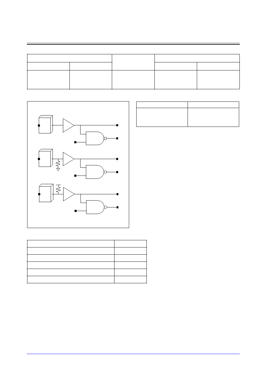
Samsung ASIC
4-11
STDL130
PvIC_LP/PvICD_LP/PvICU_LP
Input Buffers
Cell Availability
Logic Symbol
Standard Load (SL)
1.8V Interface
2.5V Interface
3.3V Interface
1.8V Interface
3.3V-Tolerant
3.3V Interface
5V-Tolerant
PIC_LP
PICD_LP
PICU_LP
PTIC_LP
PTICD_LP
PTICU_LP
PMIC_LP
PMICD_LP
PMICU_LP
PHIC_LP
PHICD_LP
PHICU_LP
PHTIC_LP
PHTICD_LP
PHTICU_LP
Cell Name
PI
PIC_LP/PICD_LP/PICU_LP
3.79
PTIC_LP/PTICD_LP/PTICU_LP
3.79
PMIC_LP/PMICD_LP/PMICU_LP
3.74
PHIC_LP/PHICD_LP/PHICU_LP
3.74
PHTIC_LP/PHTICD_LP/PHTICU_LP
3.74
Truth Table
PAD
PI
Y
PO
1
1
1
0
0
x
0
1
1
0
1
1
Y
PO
PI
PAD
Y
PO
PI
PAD
Y
PO
PI
PAD
PvIC_LP
PvICD_LP
PvICU_LP

STDL130
4-12
Samsung ASIC
PvIC_LP/PvICD_LP/PvICU_LP
Input Buffers
Switching Characteristics
(Typical process, 25
∞
C, 1.8V, t
R
/t
F
= 1.50ns, SL: Standard Load)
PIC_LP
PICD_LP
PICU_LP
NOTE:
The delay measure point of CMOS input buffer is from PAD(VDD/2) to Y(VDD/2).
Path
Parameter
Delay [ns]
SL = 2
Delay Equations [ns]
Group1*
Group2*
Group3*
PAD to Y
tR
0.120
0.112 + 0.004*SL
0.112 + 0.004*SL
0.110 + 0.004*SL
tF
0.106
0.098 + 0.004*SL
0.098 + 0.004*SL
0.091 + 0.004*SL
tPLH
0.388
0.380 + 0.004*SL
0.385 + 0.003*SL
0.402 + 0.002*SL
tPHL
0.383
0.375 + 0.004*SL
0.379 + 0.003*SL
0.393 + 0.002*SL
*Group1 : SL < 4, *Group2 : 4 SL
<
<
=
= 27, *Group3 : 27 < SL
Path
Parameter
Delay [ns]
SL = 2
Delay Equations [ns]
Group1*
Group2*
Group3*
PAD to Y
tR
0.119
0.111 + 0.004*SL
0.111 + 0.004*SL
0.109 + 0.004*SL
tF
0.107
0.098 + 0.004*SL
0.100 + 0.004*SL
0.091 + 0.004*SL
tPLH
0.412
0.404 + 0.004*SL
0.409 + 0.003*SL
0.426 + 0.002*SL
tPHL
0.377
0.369 + 0.004*SL
0.373 + 0.003*SL
0.387 + 0.002*SL
*Group1 : SL < 4, *Group2 : 4 SL
<
<
=
= 27, *Group3 : 27 < SL
Path
Parameter
Delay [ns]
SL = 2
Delay Equations [ns]
Group1*
Group2*
Group3*
PAD to Y
tR
0.110
0.103 + 0.003*SL
0.104 + 0.003*SL
0.101 + 0.003*SL
tF
0.092
0.084 + 0.004*SL
0.085 + 0.004*SL
0.082 + 0.004*SL
tPLH
0.263
0.256 + 0.003*SL
0.260 + 0.002*SL
0.275 + 0.002*SL
tPHL
0.278
0.271 + 0.003*SL
0.274 + 0.003*SL
0.285 + 0.002*SL
*Group1 : SL < 4, *Group2 : 4 SL
<
<
=
= 28, *Group3 : 28 < SL

Samsung ASIC
4-13
STDL130
PvIC_LP/PvICD_LP/PvICU_LP
Input Buffers
Switching Characteristics
(Typical process, 25
∞
C, 1.8V, t
R
/t
F
= 1.50ns, SL: Standard Load)
PTIC_LP
PTICD_LP
PTICU_LP
NOTE:
The delay measure point of CMOS input buffer is from PAD(VDD/2) to Y(VDD/2).
Path
Parameter
Delay [ns]
SL = 2
Delay Equations [ns]
Group1*
Group2*
Group3*
PAD to Y
tR
0.258
0.248 + 0.005*SL
0.252 + 0.004*SL
0.282 + 0.003*SL
tF
0.115
0.106 + 0.005*SL
0.108 + 0.004*SL
0.109 + 0.004*SL
tPLH
1.064
1.053 + 0.005*SL
1.059 + 0.004*SL
1.095 + 0.003*SL
tPHL
0.657
0.650 + 0.004*SL
0.653 + 0.003*SL
0.666 + 0.003*SL
*Group1 : SL < 4, *Group2 : 4 SL
<
<
=
= 27, *Group3 : 27 < SL
Path
Parameter
Delay [ns]
SL = 2
Delay Equations [ns]
Group1*
Group2*
Group3*
PAD to Y
tR
0.258
0.248 + 0.005*SL
0.252 + 0.004*SL
0.281 + 0.003*SL
tF
0.117
0.109 + 0.004*SL
0.109 + 0.004*SL
0.111 + 0.004*SL
tPLH
1.093
1.082 + 0.005*SL
1.088 + 0.004*SL
1.124 + 0.003*SL
tPHL
0.652
0.645 + 0.004*SL
0.648 + 0.003*SL
0.662 + 0.003*SL
*Group1 : SL < 4, *Group2 : 4 SL
<
<
=
= 27, *Group3 : 27 < SL
Path
Parameter
Delay [ns]
SL = 2
Delay Equations [ns]
Group1*
Group2*
Group3*
PAD to Y
tR
0.198
0.189 + 0.005*SL
0.193 + 0.003*SL
0.217 + 0.003*SL
tF
0.109
0.100 + 0.005*SL
0.102 + 0.004*SL
0.103 + 0.004*SL
tPLH
0.864
0.855 + 0.005*SL
0.860 + 0.004*SL
0.893 + 0.002*SL
tPHL
0.734
0.727 + 0.004*SL
0.730 + 0.003*SL
0.743 + 0.003*SL
*Group1 : SL < 4, *Group2 : 4 SL
<
<
=
= 27, *Group3 : 27 < SL
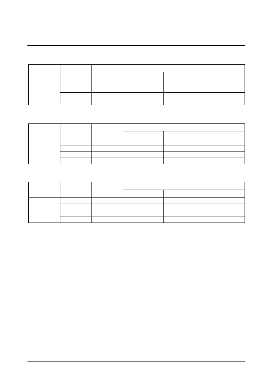
STDL130
4-14
Samsung ASIC
PvIC_LP/PvICD_LP/PvICU_LP
Input Buffers
Switching Characteristics
(Typical process, 25
∞
C, 1.8V, 2.5V, t
R
/t
F
= 1.50ns, SL: Standard Load)
PMIC_LP
PMICD_LP
PMICU_LP
NOTE:
The delay measure point of CMOS input buffer is from PAD(VDD/2) to Y(VDD/2).
Path
Parameter
Delay [ns]
SL = 2
Delay Equations [ns]
Group1*
Group2*
Group3*
PAD to Y
tR
0.158
0.140 + 0.009*SL
0.139 + 0.009*SL
0.141 + 0.009*SL
tF
0.096
0.083 + 0.006*SL
0.084 + 0.006*SL
0.082 + 0.006*SL
tPLH
0.582
0.568 + 0.007*SL
0.574 + 0.005*SL
0.589 + 0.005*SL
tPHL
0.720
0.710 + 0.005*SL
0.713 + 0.004*SL
0.725 + 0.004*SL
*Group1 : SL < 4, *Group2 : 4 SL
<
<
=
= 27, *Group3 : 27 < SL
Path
Parameter
Delay [ns]
SL = 2
Delay Equations [ns]
Group1*
Group2*
Group3*
PAD to Y
tR
0.158
0.139 + 0.009*SL
0.139 + 0.010*SL
0.141 + 0.009*SL
tF
0.096
0.083 + 0.006*SL
0.084 + 0.006*SL
0.082 + 0.006*SL
tPLH
0.598
0.584 + 0.007*SL
0.590 + 0.005*SL
0.605 + 0.005*SL
tPHL
0.714
0.704 + 0.005*SL
0.707 + 0.004*SL
0.719 + 0.004*SL
*Group1 : SL < 4, *Group2 : 4 SL
<
<
=
= 27, *Group3 : 27 < SL
Path
Parameter
Delay [ns]
SL = 2
Delay Equations [ns]
Group1*
Group2*
Group3*
PAD to Y
tR
0.158
0.140 + 0.009*SL
0.139 + 0.010*SL
0.141 + 0.009*SL
tF
0.096
0.083 + 0.006*SL
0.084 + 0.006*SL
0.083 + 0.006*SL
tPLH
0.573
0.559 + 0.007*SL
0.565 + 0.005*SL
0.580 + 0.005*SL
tPHL
0.734
0.724 + 0.005*SL
0.728 + 0.004*SL
0.739 + 0.004*SL
*Group1 : SL < 4, *Group2 : 4 SL
<
<
=
= 27, *Group3 : 27 < SL

Samsung ASIC
4-15
STDL130
PvIC_LP/PvICD_LP/PvICU_LP
Input Buffers
Switching Characteristics
(Typical process, 25
∞
C, 1.8V, 3.3V, t
R
/t
F
= 1.50ns, SL: Standard Load)
PHIC_LP
PHICD_LP
PHICU_LP
NOTE:
The delay measure point of LVCMOS input buffer is from PAD(VDD/2) to Y(VDD/2).
Path
Parameter
Delay [ns]
SL = 2
Delay Equations [ns]
Group1*
Group2*
Group3*
PAD to Y
tR
0.211
0.199 + 0.006*SL
0.203 + 0.005*SL
0.190 + 0.006*SL
tF
0.110
0.097 + 0.006*SL
0.098 + 0.006*SL
0.096 + 0.006*SL
tPLH
0.436
0.422 + 0.007*SL
0.432 + 0.005*SL
0.471 + 0.003*SL
tPHL
0.785
0.775 + 0.005*SL
0.778 + 0.004*SL
0.790 + 0.004*SL
*Group1 : SL < 4, *Group2 : 4 SL
<
<
=
= 27, *Group3 : 27 < SL
Path
Parameter
Delay [ns]
SL = 2
Delay Equations [ns]
Group1*
Group2*
Group3*
PAD to Y
tR
0.211
0.198 + 0.006*SL
0.203 + 0.005*SL
0.191 + 0.006*SL
tF
0.110
0.097 + 0.007*SL
0.098 + 0.006*SL
0.096 + 0.006*SL
tPLH
0.461
0.446 + 0.007*SL
0.457 + 0.005*SL
0.495 + 0.003*SL
tPHL
0.793
0.783 + 0.005*SL
0.786 + 0.004*SL
0.798 + 0.004*SL
*Group1 : SL < 4, *Group2 : 4 SL
<
<
=
= 27, *Group3 : 27 < SL
Path
Parameter
Delay [ns]
SL = 2
Delay Equations [ns]
Group1*
Group2*
Group3*
PAD to Y
tR
0.211
0.199 + 0.006*SL
0.203 + 0.005*SL
0.190 + 0.006*SL
tF
0.110
0.098 + 0.006*SL
0.098 + 0.006*SL
0.097 + 0.006*SL
tPLH
0.427
0.412 + 0.007*SL
0.423 + 0.005*SL
0.461 + 0.003*SL
tPHL
0.800
0.790 + 0.005*SL
0.793 + 0.004*SL
0.805 + 0.004*SL
*Group1 : SL < 4, *Group2 : 4 SL
<
<
=
= 27, *Group3 : 27 < SL

STDL130
4-16
Samsung ASIC
PvIC_LP/PvICD_LP/PvICU_LP
Input Buffers
Switching Characteristics
(Typical process, 25
∞
C, 1.8V, 3.3V, t
R
/t
F
= 1.50ns, SL: Standard Load)
PHTIC_LP
PHTICD_LP
PHTICU_LP
NOTE:
The delay measure point of LVCMOS input buffer is from PAD(VDD/2) to Y(VDD/2).
Path
Parameter
Delay [ns]
SL = 2
Delay Equations [ns]
Group1*
Group2*
Group3*
PAD to Y
tR
0.211
0.198 + 0.006*SL
0.203 + 0.005*SL
0.190 + 0.006*SL
tF
0.110
0.097 + 0.007*SL
0.098 + 0.006*SL
0.097 + 0.006*SL
tPLH
0.557
0.543 + 0.007*SL
0.553 + 0.005*SL
0.591 + 0.003*SL
tPHL
0.882
0.872 + 0.005*SL
0.875 + 0.004*SL
0.887 + 0.004*SL
*Group1 : SL < 4, *Group2 : 4 SL
<
<
=
= 27, *Group3 : 27 < SL
Path
Parameter
Delay [ns]
SL = 2
Delay Equations [ns]
Group1*
Group2*
Group3*
PAD to Y
tR
0.211
0.198 + 0.006*SL
0.203 + 0.005*SL
0.191 + 0.006*SL
tF
0.110
0.097 + 0.006*SL
0.098 + 0.006*SL
0.097 + 0.006*SL
tPLH
0.585
0.570 + 0.007*SL
0.581 + 0.005*SL
0.619 + 0.003*SL
tPHL
0.886
0.876 + 0.005*SL
0.879 + 0.004*SL
0.891 + 0.004*SL
*Group1 : SL < 4, *Group2 : 4 SL
<
<
=
= 27, *Group3 : 27 < SL
Path
Parameter
Delay [ns]
SL = 2
Delay Equations [ns]
Group1*
Group2*
Group3*
PAD to Y
tR
0.211
0.199 + 0.006*SL
0.203 + 0.005*SL
0.190 + 0.006*SL
tF
0.110
0.098 + 0.006*SL
0.098 + 0.006*SL
0.097 + 0.006*SL
tPLH
0.540
0.525 + 0.007*SL
0.536 + 0.005*SL
0.574 + 0.003*SL
tPHL
0.961
0.952 + 0.005*SL
0.955 + 0.004*SL
0.967 + 0.004*SL
*Group1 : SL < 4, *Group2 : 4 SL
<
<
=
= 27, *Group3 : 27 < SL
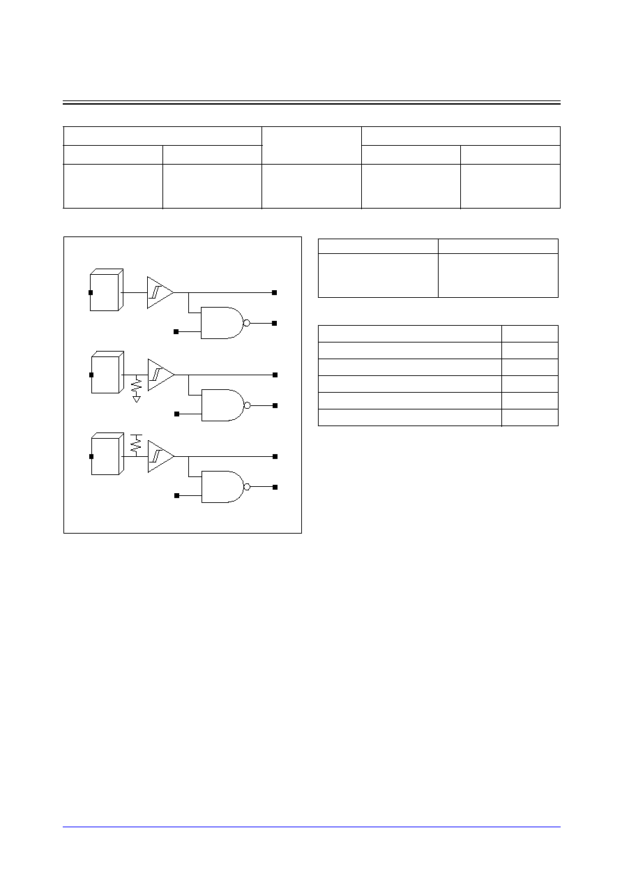
Samsung ASIC
4-17
STDL130
PvIS_LP/PvISD_LP_LP/PvISU_LP
Schmitt Trigger Level Input Buffers
Cell Availability
Logic Symbol
1.8V Interface
2.5V Interface
3.3V Interface
1.8V Interface
3.3V-Tolerant
3.3V Interface
5V-Tolerant
PIS_LP
PISD_LP
PISU_LP
PTIS_LP
PTISD_LP
PTISU_LP
PMIS_LP
PMISD_LP
PMISU_LP
PHIS_LP
PHISD_LP
PHISU_LP
PHTIS_LP
PHTISD_LP
PHTISU_LP
Truth Table
Standard Load (SL)
PAD
PI
Y
PO
1
1
1
0
0
x
0
1
1
0
1
1
Cell Name
PI
PIS_LP/PISD_LP/PISU_LP
3.79
PTIS_LP/PTISD_LP/PTISU_LP
3.79
PMIS_LP/PMISD_LP/PMISU_LP
3.74
PHIS_LP/PHISD_LP/PHISU_LP
3.74
PHTIS_LP/PHTISD_LP/PHTISU_LP
3.74
Y
PO
PI
PAD
Y
PO
PI
PAD
Y
PO
PI
PAD
PvIS_LP
PvISD_LP
PvISU_LP

STDL130
4-18
Samsung ASIC
PvIS_LP/PvISD_LP/PvISU_LP
Schmitt Trigger Level Input Buffers
Switching Characteristics
(Typical process, 25
∞
C, 1.8V, t
R
/t
F
= 1.50ns, SL: Standard Load)
PIS_LP
PISD_LP
PISU_LP
Path
Parameter
Delay [ns]
SL = 2
Delay Equations [ns]
Group1*
Group2*
Group3*
PAD to Y
tR
0.113
0.103 + 0.005*SL
0.106 + 0.004*SL
0.107 + 0.004*SL
tF
0.121
0.112 + 0.005*SL
0.114 + 0.004*SL
0.119 + 0.004*SL
tPLH
0.653
0.645 + 0.004*SL
0.650 + 0.003*SL
0.667 + 0.002*SL
tPHL
0.688
0.679 + 0.005*SL
0.684 + 0.003*SL
0.704 + 0.003*SL
*Group1 : SL < 4, *Group2 : 4 SL
<
<
=
= 27, *Group3 : 27 < SL
Path
Parameter
Delay [ns]
SL = 2
Delay Equations [ns]
Group1*
Group2*
Group3*
PAD to Y
tR
0.115
0.105 + 0.005*SL
0.108 + 0.004*SL
0.109 + 0.004*SL
tF
0.124
0.115 + 0.005*SL
0.117 + 0.004*SL
0.121 + 0.004*SL
tPLH
0.656
0.648 + 0.004*SL
0.652 + 0.003*SL
0.671 + 0.002*SL
tPHL
0.695
0.686 + 0.005*SL
0.691 + 0.003*SL
0.712 + 0.003*SL
*Group1 : SL < 4, *Group2 : 4 SL
<
<
=
= 27, *Group3 : 27 < SL
Path
Parameter
Delay [ns]
SL = 2
Delay Equations [ns]
Group1*
Group2*
Group3*
PAD to Y
tR
0.114
0.104 + 0.005*SL
0.106 + 0.004*SL
0.108 + 0.004*SL
tF
0.122
0.111 + 0.005*SL
0.115 + 0.004*SL
0.119 + 0.004*SL
tPLH
0.658
0.650 + 0.004*SL
0.654 + 0.003*SL
0.673 + 0.002*SL
tPHL
0.703
0.694 + 0.005*SL
0.699 + 0.003*SL
0.720 + 0.003*SL
*Group1 : SL < 4, *Group2 : 4 SL
<
<
=
= 27, *Group3 : 27 < SL
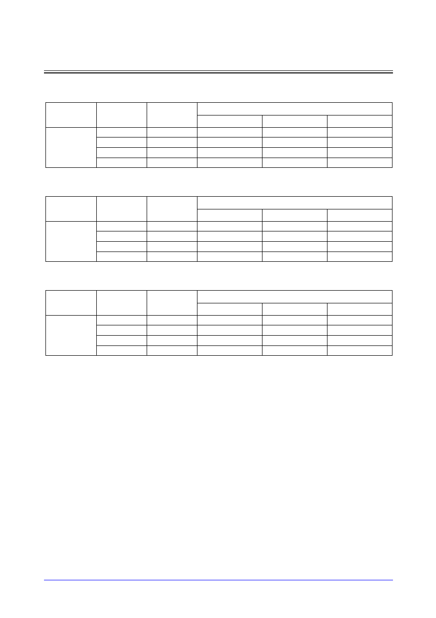
Samsung ASIC
4-19
STDL130
PvIS_LP/PvISD_LP/PvISU_LP
Schmitt Trigger Level Input Buffers
Switching Characteristics
(Typical process, 25
∞
C, 1.8V, t
R
/t
F
= 1.50ns, SL: Standard Load)
PTIS_LP
PTISD_LP
PTISU_LP
NOTE:
The delay measure point of LVCMOS input buffer is from PAD(VDD/2) to Y(VDD/2).
Path
Parameter
Delay [ns]
SL = 2
Delay Equations [ns]
Group1*
Group2*
Group3*
PAD to Y
tR
0.295
0.280 + 0.007*SL
0.286 + 0.006*SL
0.332 + 0.004*SL
tF
0.113
0.104 + 0.005*SL
0.106 + 0.004*SL
0.110 + 0.004*SL
tPLH
2.139
2.124 + 0.008*SL
2.132 + 0.006*SL
2.184 + 0.004*SL
tPHL
0.835
0.826 + 0.004*SL
0.830 + 0.003*SL
0.850 + 0.003*SL
*Group1 : SL < 4, *Group2 : 4 SL
<
<
=
= 27, *Group3 : 27 < SL
Path
Parameter
Delay [ns]
SL = 2
Delay Equations [ns]
Group1*
Group2*
Group3*
PAD to Y
tR
0.295
0.281 + 0.007*SL
0.286 + 0.006*SL
0.332 + 0.004*SL
tF
0.115
0.106 + 0.005*SL
0.108 + 0.004*SL
0.112 + 0.004*SL
tPLH
2.167
2.152 + 0.008*SL
2.160 + 0.006*SL
2.212 + 0.004*SL
tPHL
0.836
0.827 + 0.004*SL
0.831 + 0.003*SL
0.851 + 0.003*SL
*Group1 : SL < 4, *Group2 : 4 SL
<
<
=
= 27, *Group3 : 27 < SL
Path
Parameter
Delay [ns]
SL = 2
Delay Equations [ns]
Group1*
Group2*
Group3*
PAD to Y
tR
0.187
0.174 + 0.006*SL
0.181 + 0.005*SL
0.202 + 0.004*SL
tF
0.111
0.101 + 0.005*SL
0.104 + 0.004*SL
0.108 + 0.004*SL
tPLH
1.154
1.142 + 0.006*SL
1.149 + 0.004*SL
1.187 + 0.003*SL
tPHL
0.875
0.866 + 0.004*SL
0.871 + 0.003*SL
0.890 + 0.003*SL
*Group1 : SL < 4, *Group2 : 4 SL
<
<
=
= 27, *Group3 : 27 < SL

STDL130
4-20
Samsung ASIC
PvIS_LP/PvISD_LP/PvISU_LP
Schmitt Trigger Level Input Buffers
Switching Characteristics
(Typical process, 25
∞
C, 1.8V, 2.5V, t
R
/t
F
= 1.50ns, SL: Standard Load)
PMIS_LP
PMISD_LP
PMISU_LP
Path
Parameter
Delay [ns]
SL = 2
Delay Equations [ns]
Group1*
Group2*
Group3*
PAD to Y
tR
0.158
0.140 + 0.009*SL
0.139 + 0.009*SL
0.140 + 0.009*SL
tF
0.096
0.083 + 0.006*SL
0.084 + 0.006*SL
0.082 + 0.006*SL
tPLH
0.784
0.770 + 0.007*SL
0.776 + 0.005*SL
0.791 + 0.005*SL
tPHL
1.141
1.131 + 0.005*SL
1.134 + 0.004*SL
1.146 + 0.004*SL
*Group1 : SL < 4, *Group2 : 4 SL
<
<
=
= 27, *Group3 : 27 < SL
Path
Parameter
Delay [ns]
SL = 2
Delay Equations [ns]
Group1*
Group2*
Group3*
PAD to Y
tR
0.158
0.140 + 0.009*SL
0.139 + 0.009*SL
0.141 + 0.009*SL
tF
0.096
0.083 + 0.006*SL
0.084 + 0.006*SL
0.082 + 0.006*SL
tPLH
0.789
0.775 + 0.007*SL
0.781 + 0.005*SL
0.796 + 0.005*SL
tPHL
1.159
1.149 + 0.005*SL
1.152 + 0.004*SL
1.164 + 0.004*SL
*Group1 : SL < 4, *Group2 : 4 SL
<
<
=
= 27, *Group3 : 27 < SL
Path
Parameter
Delay [ns]
SL = 2
Delay Equations [ns]
Group1*
Group2*
Group3*
PAD to Y
tR
0.158
0.140 + 0.009*SL
0.139 + 0.009*SL
0.140 + 0.009*SL
tF
0.096
0.083 + 0.006*SL
0.084 + 0.006*SL
0.082 + 0.006*SL
tPLH
0.787
0.773 + 0.007*SL
0.779 + 0.005*SL
0.794 + 0.005*SL
tPHL
1.148
1.139 + 0.005*SL
1.142 + 0.004*SL
1.153 + 0.004*SL
*Group1 : SL < 4, *Group2 : 4 SL
<
<
=
= 27, *Group3 : 27 < SL

Samsung ASIC
4-21
STDL130
PvIS_LP/PvISD_LP/PvISU_LP
Schmitt Trigger Level Input Buffers
Switching Characteristics
(Typical process, 25
∞
C, 1.8V, 3.3V, t
R
/t
F
= 1.50ns, SL: Standard Load)
PHIS_LP
PHISD_LP
PHISU_LP
Path
Parameter
Delay [ns]
SL = 2
Delay Equations [ns]
Group1*
Group2*
Group3*
PAD to Y
tR
0.212
0.199 + 0.006*SL
0.203 + 0.005*SL
0.192 + 0.006*SL
tF
0.110
0.097 + 0.006*SL
0.098 + 0.006*SL
0.097 + 0.006*SL
tPLH
0.693
0.678 + 0.007*SL
0.689 + 0.005*SL
0.728 + 0.003*SL
tPHL
1.127
1.118 + 0.005*SL
1.121 + 0.004*SL
1.133 + 0.004*SL
*Group1 : SL < 4, *Group2 : 4 SL
<
<
=
= 27, *Group3 : 27 < SL
Path
Parameter
Delay [ns]
SL = 2
Delay Equations [ns]
Group1*
Group2*
Group3*
PAD to Y
tR
0.212
0.200 + 0.006*SL
0.204 + 0.005*SL
0.192 + 0.006*SL
tF
0.110
0.098 + 0.006*SL
0.098 + 0.006*SL
0.097 + 0.006*SL
tPLH
0.706
0.691 + 0.008*SL
0.702 + 0.005*SL
0.740 + 0.003*SL
tPHL
1.158
1.148 + 0.005*SL
1.151 + 0.004*SL
1.163 + 0.004*SL
*Group1 : SL < 4, *Group2 : 4 SL
<
<
=
= 27, *Group3 : 27 < SL
Path
Parameter
Delay [ns]
SL = 2
Delay Equations [ns]
Group1*
Group2*
Group3*
PAD to Y
tR
0.212
0.199 + 0.006*SL
0.204 + 0.005*SL
0.191 + 0.006*SL
tF
0.110
0.098 + 0.006*SL
0.098 + 0.006*SL
0.097 + 0.006*SL
tPLH
0.698
0.684 + 0.007*SL
0.694 + 0.005*SL
0.733 + 0.003*SL
tPHL
1.156
1.147 + 0.005*SL
1.150 + 0.004*SL
1.161 + 0.004*SL
*Group1 : SL < 4, *Group2 : 4 SL
<
<
=
= 27, *Group3 : 27 < SL
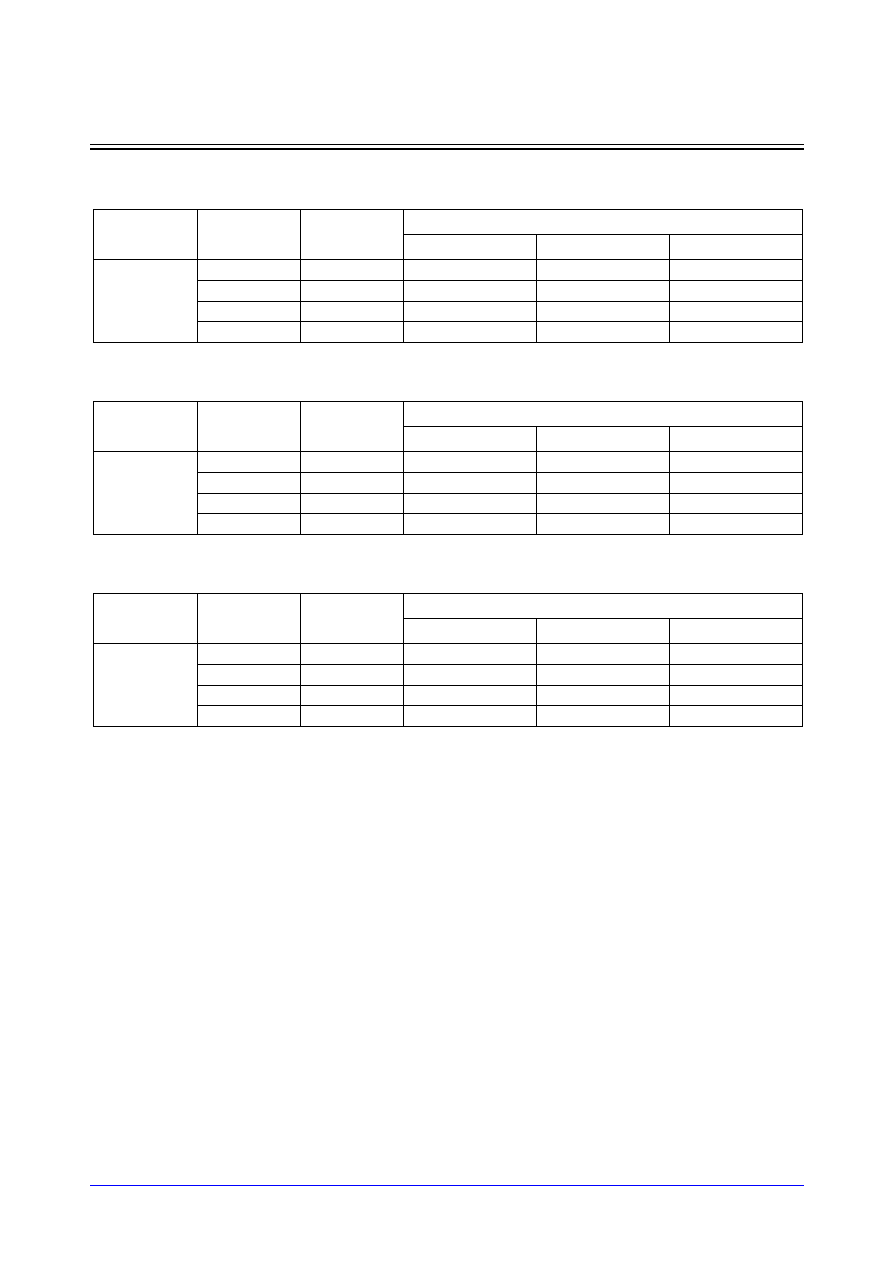
STDL130
4-22
Samsung ASIC
PvIS_LP/PvISD_LP/PvISU_LP
Schmitt Trigger Level Input Buffers
Switching Characteristics
(Typical process, 25
∞
C, 1.8V, 3.3V, t
R
/t
F
= 1.50ns, SL: Standard Load)
PHTIS_LP
PHTISD_LP
PHTISU_LP
Path
Parameter
Delay [ns]
SL = 2
Delay Equations [ns]
Group1*
Group2*
Group3*
PAD to Y
tR
0.210
0.197 + 0.006*SL
0.202 + 0.005*SL
0.190 + 0.006*SL
tF
0.110
0.098 + 0.006*SL
0.098 + 0.006*SL
0.096 + 0.006*SL
tPLH
1.001
0.986 + 0.007*SL
0.997 + 0.005*SL
1.035 + 0.003*SL
tPHL
1.264
1.254 + 0.005*SL
1.257 + 0.004*SL
1.269 + 0.004*SL
*Group1 : SL < 4, *Group2 : 4 SL
<
<
=
= 27, *Group3 : 27 < SL
Path
Parameter
Delay [ns]
SL = 2
Delay Equations [ns]
Group1*
Group2*
Group3*
PAD to Y
tR
0.210
0.198 + 0.006*SL
0.201 + 0.005*SL
0.190 + 0.006*SL
tF
0.110
0.097 + 0.006*SL
0.098 + 0.006*SL
0.097 + 0.006*SL
tPLH
0.993
0.978 + 0.007*SL
0.989 + 0.005*SL
1.027 + 0.003*SL
tPHL
1.297
1.287 + 0.005*SL
1.290 + 0.004*SL
1.302 + 0.004*SL
*Group1 : SL < 4, *Group2 : 4 SL
<
<
=
= 27, *Group3 : 27 < SL
Path
Parameter
Delay [ns]
SL = 2
Delay Equations [ns]
Group1*
Group2*
Group3*
PAD to Y
tR
0.211
0.198 + 0.006*SL
0.203 + 0.005*SL
0.190 + 0.006*SL
tF
0.110
0.097 + 0.006*SL
0.098 + 0.006*SL
0.096 + 0.006*SL
tPLH
1.077
1.062 + 0.007*SL
1.072 + 0.005*SL
1.111 + 0.003*SL
tPHL
1.291
1.281 + 0.005*SL
1.284 + 0.004*SL
1.296 + 0.004*SL
*Group1 : SL < 4, *Group2 : 4 SL
<
<
=
= 27, *Group3 : 27 < SL
Samsung ASIC
4-23
STDL130
OUTPUT BUFFERS
Cell List
Cell Name
Function Description
POB(1/2/4/8/12/16/20/24)_LP
1.8V CMOS Normal Output Buffers
POB(4/8/12/16/20/24)SM_LP
1.8V CMOS Normal Output Buffers with Medium Slew-Rate
POB(12/16/20/24)SH_LP
1.8V CMOS Normal Output Buffers with High Slew-Rate
PMOB(1/2/4/8/12/16/20/24)_LP
2.5V CMOS Normal Output Buffers
PMOB(4/8/12/16/20/24)SM_LP
2.5V CMOS Normal Output Buffers with Medium Slew-Rate
PMOB(12/16/20/24)SH_LP
2.5V CMOS Normal Output Buffers with High Slew-Rate
PHOB(1/2/4/8/12/16/20/24)_LP
3.3V LVCMOS Normal Output Buffers
PHOB(4/8/12/16/20/24)SM_LP
3.3V LVCMOS Normal Output Buffers with Medium Slew-Rate
PHOB(12/16/20/24)SH_LP
3.3V LVCMOS Normal Output Buffers with High Slew-Rate
POD(1/2/4/8/12/16/20/24)_LP
1.8V CMOS Open Drain Output Buffers
POD(4/8/12/16/20/24)SM_LP
1.8V CMOS Open Drain Output Buffers with Medium Slew-Rate
POD(12/16/20/24)SH_LP
1.8V CMOS Open Drain Output Buffers with High Slew-Rate
PMOD(1/2/4/8/12/16/20/24)_LP
2.5V CMOS Open Drain Output Buffers
PMOD(4/8/12/16/20/24)SM_LP
2.5V CMOS Open Drain Output Buffers with Medium Slew-Rate
PMOD(12/16/20/24)SH_LP
2.5V CMOS Open Drain Output Buffers with High Slew-Rate
PHOD(1/2/4/8/12/16/20/24)_LP
3.3V LVCMOS Open Drain Output Buffers
PHOD(4/8/12/16/20/24)SM_LP
3.3V LVCMOS Open Drain Output Buffers with Medium Slew-Rate
PHOD(12/16/20/24)SH_LP
3.3V LVCMOS Open Drain Output Buffers with High Slew-Rate
POT(1/2/4/8/12/16/20/24)_LP
1.8V CMOS Tri-State Output Buffers
POT(4/8/12/16/20/24)SM_LP
1.8V CMOS Tri-State Output Buffers with Medium Slew-Rate
POT(12/16/20/24)SH_LP
1.8V CMOS Tri-State Output Buffers with High Slew-Rate
PMOT(1/2/4/8/12/16/20/24)_LP
2.5V CMOS Tri-State Output Buffers
PMOT(4/8/12/16/20/24)SM_LP
2.5V CMOS Tri-State Output Buffers with Medium Slew-Rate
PMO(12/16/20/24)SH_LP
2.5V CMOS Tri-State Output Buffers with High Slew-Rate
PHOT(1/2/4/8/12/16/20/24)_LP
3.3V LVCMOS Tri-State Output Buffers
PHOT(4/8/12/16/20/24)SM_LP
3.3V LVCMOS Tri-State Output Buffers with Medium Slew-Rate
PHOT(12/16/20/24)SH_LP
3.3V LVCMOS Tri-State Output Buffers with High Slew-Rate
PTOD(1/2/4/6)_LP
3.3V-Tolerant for 1.8V Interface Open Drain Output Buffers
PTOD(4/6)SM_LP
3.3V-Tolerant for 1.8V Interface Open Drain Output with Medium Slew-Rate
PHTOD(1/2/4/6)_LP
5V-Tolerant for 3.3V Interface Open Drain Output Buffers
PHTOD(4/6)SM_LP
5V-Tolerant for 3.3V Interface Open Drain Output with Medium Slew-Rate
PTOT(1/2/4/6)_LP
3.3V-Tolerant for 1.8V Interface Tri-State Output Buffers
PTOT(4/6)SM_LP
3.3V-Tolerant for 1.8V Interface Tri-State Output with Medium Slew-Rate
PHTOT(1/2/4/6)_LP
5V-Tolerant for 3.3V Interface Tri-State Output Buffers
PHTOT(4/6)SM_LP
5V-Tolerant for 3.3V Interface Tri-State Output with Medium Slew-Rate
STDL130
4-24
Samsung ASIC
PvOByz_LP
Normal Output Buffers
Cell Availability
Logic Symbol
Standard Load (SL)
1.8V Interface
2.5V Interface
3.3V Interface
POB(1/2/4/8/12/16/20/24)_LP
POB(4/8/12/16/20/24)SM_LP
POB(12/16/20/24)SH_LP
PMOB(1/2/4/8/12/16/20/24)_LP
PMOB(4/8/12/16/20/24)SM_LP
PMOB(12/16/20/24)SH_LP
PHOB(1/2/4/8/12/16/20/24)_LP
PHOB(4/8/12/16/20/24)SM_LP
PHOB(12/16/20/24)SH_LP
Cell Name
A
POB(1/2/4)_LP
8.16
POB(8/12/16/20/24)_LP
15.95
POB4SM_LP
21.70
POB(8/12/20/24)SM_LP
27.85
POB12SH_LP
29.05
POB16SH_LP
28.75
POB20SH_LP
26.74
POB24SH_LP
25.81
PMOB(1/2/4/8/12/16/20/24)_LP
6.32
PMOB(4/8/12/16/20/24)SM_LP
6.32
PMOB(12/16/20/24)SH_LP
6.32
PHOB(1/2/4/8/12/16/20/24)_LP
7.50
PHOB(4/8/12/16/20/24)SM_LP
7.50
PHOB(12/16/20/24)SH_LP
7.50
Truth Table
A
PAD
0
0
1
1
PAD
A

Samsung ASIC
4-25
STDL130
PvOByz_LP
Normal Output Buffers
Switching Characteristics
(Typical process, 25
∞
C, 1.8V, t
R
/t
F
= 0.20ns, CL: Capacitive Load[pF])
POB1_LP
POB2_LP
POB4_LP
POB8_LP
Path
Parameter
Delay [ns]
CL = 50.0pF
Delay Equations [ns]
Group1*
Group2*
Group3*
A to PAD
tR
20.443
1.560 + 0.378*CL
1.557 + 0.378*CL
1.554 + 0.378*CL
tF
23.041
1.821 + 0.424*CL
1.811 + 0.425*CL
1.811 + 0.425*CL
tPLH
9.823
0.909 + 0.178*CL
0.909 + 0.178*CL
0.909 + 0.178*CL
tPHL
12.404
1.537 + 0.217*CL
1.538 + 0.217*CL
1.535 + 0.217*CL
*Group1 : CL < 50, *Group2 : 50 CL
<
<
=
= 75, *Group3 : 75 < CL
Path
Parameter
Delay [ns]
CL = 50.0pF
Delay Equations [ns]
Group1*
Group2*
Group3*
A to PAD
tR
13.759
1.082 + 0.254*CL
1.081 + 0.254*CL
1.078 + 0.254*CL
tF
12.208
0.976 + 0.225*CL
0.968 + 0.225*CL
0.962 + 0.225*CL
tPLH
6.850
0.782 + 0.121*CL
0.783 + 0.121*CL
0.782 + 0.121*CL
tPHL
6.741
0.889 + 0.117*CL
0.890 + 0.117*CL
0.890 + 0.117*CL
*Group1 : CL < 50, *Group2 : 50 CL
<
<
=
= 75, *Group3 : 75 < CL
Path
Parameter
Delay [ns]
CL = 50.0pF
Delay Equations [ns]
Group1*
Group2*
Group3*
A to PAD
tR
6.856
0.564 + 0.126*CL
0.563 + 0.126*CL
0.562 + 0.126*CL
tF
6.905
0.572 + 0.127*CL
0.570 + 0.127*CL
0.562 + 0.127*CL
tPLH
3.495
0.520 + 0.059*CL
0.523 + 0.059*CL
0.524 + 0.059*CL
tPHL
3.980
0.564 + 0.068*CL
0.566 + 0.068*CL
0.567 + 0.068*CL
*Group1 : CL < 50, *Group2 : 50 CL
<
<
=
= 75, *Group3 : 75 < CL
Path
Parameter
Delay [ns]
CL = 50.0pF
Delay Equations [ns]
Group1*
Group2*
Group3*
A to PAD
tR
3.439
0.292 + 0.063*CL
0.292 + 0.063*CL
0.292 + 0.063*CL
tF
3.462
0.295 + 0.063*CL
0.294 + 0.063*CL
0.293 + 0.063*CL
tPLH
1.877
0.388 + 0.030*CL
0.389 + 0.030*CL
0.391 + 0.030*CL
tPHL
2.109
0.400 + 0.034*CL
0.402 + 0.034*CL
0.403 + 0.034*CL
*Group1 : CL < 50, *Group2 : 50 CL
<
<
=
= 75, *Group3 : 75 < CL
STDL130
4-26
Samsung ASIC
PvOByz_LP
Normal Output Buffers
Switching Characteristics
(Typical process, 25
∞
C, 1.8V, t
R
/t
F
= 0.20ns, CL: Capacitive Load[pF])
POB12_LP
POB16_LP
POB20_LP
POB24_LP
Path
Parameter
Delay [ns]
CL = 50.0pF
Delay Equations [ns]
Group1*
Group2*
Group3*
A to PAD
tR
2.312
0.226 + 0.042*CL
0.217 + 0.042*CL
0.213 + 0.042*CL
tF
2.326
0.229 + 0.042*CL
0.218 + 0.042*CL
0.214 + 0.042*CL
tPLH
1.427
0.433 + 0.020*CL
0.434 + 0.020*CL
0.436 + 0.020*CL
tPHL
1.558
0.426 + 0.023*CL
0.423 + 0.023*CL
0.421 + 0.023*CL
*Group1 : CL < 50, *Group2 : 50 CL
<
<
=
= 75, *Group3 : 75 < CL
Path
Parameter
Delay [ns]
CL = 50.0pF
Delay Equations [ns]
Group1*
Group2*
Group3*
A to PAD
tR
1.762
0.219 + 0.031*CL
0.202 + 0.031*CL
0.190 + 0.031*CL
tF
1.773
0.236 + 0.031*CL
0.209 + 0.031*CL
0.190 + 0.032*CL
tPLH
1.246
0.497 + 0.015*CL
0.500 + 0.015*CL
0.502 + 0.015*CL
tPHL
1.323
0.487 + 0.017*CL
0.478 + 0.017*CL
0.472 + 0.017*CL
*Group1 : CL < 50, *Group2 : 50 CL
<
<
=
= 75, *Group3 : 75 < CL
Path
Parameter
Delay [ns]
CL = 50.0pF
Delay Equations [ns]
Group1*
Group2*
Group3*
A to PAD
tR
1.447
0.235 + 0.024*CL
0.214 + 0.025*CL
0.197 + 0.025*CL
tF
1.464
0.274 + 0.024*CL
0.237 + 0.025*CL
0.209 + 0.025*CL
tPLH
1.171
0.564 + 0.012*CL
0.572 + 0.012*CL
0.575 + 0.012*CL
tPHL
1.217
0.565 + 0.013*CL
0.551 + 0.013*CL
0.541 + 0.013*CL
*Group1 : CL < 50, *Group2 : 50 CL
<
<
=
= 75, *Group3 : 75 < CL
Path
Parameter
Delay [ns]
CL = 50.0pF
Delay Equations [ns]
Group1*
Group2*
Group3*
A to PAD
tR
1.252
0.261 + 0.020*CL
0.240 + 0.020*CL
0.220 + 0.021*CL
tF
1.280
0.333 + 0.019*CL
0.285 + 0.020*CL
0.249 + 0.020*CL
tPLH
1.147
0.628 + 0.010*CL
0.644 + 0.010*CL
0.651 + 0.010*CL
tPHL
1.178
0.646 + 0.011*CL
0.635 + 0.011*CL
0.621 + 0.011*CL
*Group1 : CL < 50, *Group2 : 50 CL
<
<
=
= 75, *Group3 : 75 < CL

Samsung ASIC
4-27
STDL130
PvOByz_LP
Normal Output Buffers
Switching Characteristics
(Typical process, 25
∞
C, 1.8V, t
R
/t
F
= 0.20ns, CL: Capacitive Load[pF])
POB4SM_LP
POB8SM_LP
POB12SM_LP
Path
Parameter
Delay [ns]
CL = 50.0pF
Delay Equations [ns]
Group1*
Group2*
Group3*
A to PAD
tR
6.988
0.791 + 0.124*CL
0.743 + 0.125*CL
0.711 + 0.125*CL
tF
6.965
0.672 + 0.126*CL
0.654 + 0.126*CL
0.635 + 0.126*CL
tPLH
4.341
1.344 + 0.060*CL
1.360 + 0.060*CL
1.369 + 0.059*CL
tPHL
4.400
0.970 + 0.069*CL
0.983 + 0.068*CL
0.987 + 0.068*CL
*Group1 : CL < 50, *Group2 : 50 CL
<
<
=
= 75, *Group3 : 75 < CL
Path
Parameter
Delay [ns]
CL = 50.0pF
Delay Equations [ns]
Group1*
Group2*
Group3*
A to PAD
tR
3.896
0.908 + 0.060*CL
0.875 + 0.060*CL
0.827 + 0.061*CL
tF
3.917
0.908 + 0.060*CL
0.889 + 0.061*CL
0.842 + 0.061*CL
tPLH
3.542
1.903 + 0.033*CL
1.990 + 0.031*CL
2.044 + 0.030*CL
tPHL
3.748
1.860 + 0.038*CL
1.964 + 0.036*CL
2.030 + 0.035*CL
*Group1 : CL < 50, *Group2 : 50 CL
<
<
=
= 75, *Group3 : 75 < CL
Path
Parameter
Delay [ns]
CL = 50.0pF
Delay Equations [ns]
Group1*
Group2*
Group3*
A to PAD
tR
3.480
1.427 + 0.041*CL
1.505 + 0.040*CL
1.532 + 0.039*CL
tF
3.470
1.344 + 0.043*CL
1.452 + 0.040*CL
1.516 + 0.039*CL
tPLH
3.829
2.316 + 0.030*CL
2.534 + 0.026*CL
2.715 + 0.023*CL
tPHL
3.992
2.343 + 0.033*CL
2.545 + 0.029*CL
2.725 + 0.027*CL
*Group1 : CL < 50, *Group2 : 50 CL
<
<
=
= 75, *Group3 : 75 < CL

STDL130
4-28
Samsung ASIC
PvOByz_LP
Normal Output Buffers
Switching Characteristics
(Typical process, 25
∞
C, 1.8V, t
R
/t
F
= 0.20ns, CL: Capacitive Load[pF])
POB16SM_LP
POB20SM_LP
POB24SM_LP
Path
Parameter
Delay [ns]
CL = 50.0pF
Delay Equations [ns]
Group1*
Group2*
Group3*
A to PAD
tR
2.716
1.167 + 0.031*CL
1.222 + 0.030*CL
1.246 + 0.030*CL
tF
2.738
1.072 + 0.033*CL
1.182 + 0.031*CL
1.254 + 0.030*CL
tPLH
3.607
2.451 + 0.023*CL
2.616 + 0.020*CL
2.754 + 0.018*CL
tPHL
3.816
2.519 + 0.026*CL
2.680 + 0.023*CL
2.827 + 0.021*CL
*Group1 : CL < 50, *Group2 : 50 CL
<
<
=
= 75, *Group3 : 75 < CL
Path
Parameter
Delay [ns]
CL = 50.0pF
Delay Equations [ns]
Group1*
Group2*
Group3*
A to PAD
tR
2.837
1.435 + 0.028*CL
1.551 + 0.026*CL
1.638 + 0.025*CL
tF
2.849
1.330 + 0.030*CL
1.466 + 0.028*CL
1.590 + 0.026*CL
tPLH
3.897
2.674 + 0.024*CL
2.886 + 0.020*CL
3.074 + 0.018*CL
tPHL
4.158
2.918 + 0.025*CL
3.053 + 0.022*CL
3.208 + 0.020*CL
*Group1 : CL < 50, *Group2 : 50 CL
<
<
=
= 75, *Group3 : 75 < CL
Path
Parameter
Delay [ns]
CL = 50.0pF
Delay Equations [ns]
Group1*
Group2*
Group3*
A to PAD
tR
2.628
1.444 + 0.024*CL
1.543 + 0.022*CL
1.622 + 0.021*CL
tF
2.495
1.179 + 0.026*CL
1.306 + 0.024*CL
1.425 + 0.022*CL
tPLH
4.180
3.071 + 0.022*CL
3.275 + 0.018*CL
3.455 + 0.016*CL
tPHL
4.298
3.214 + 0.022*CL
3.340 + 0.019*CL
3.483 + 0.017*CL
*Group1 : CL < 50, *Group2 : 50 CL
<
<
=
= 75, *Group3 : 75 < CL

Samsung ASIC
4-29
STDL130
PvOByz_LP
Normal Output Buffers
Switching Characteristics
(Typical process, 25
∞
C, 1.8V, t
R
/t
F
= 0.20ns, CL: Capacitive Load[pF])
POB12SH_LP
POB16SH_LP
POB20SH_LP
POB24SH_LP
Path
Parameter
Delay [ns]
CL = 50.0pF
Delay Equations [ns]
Group1*
Group2*
Group3*
A to PAD
tR
4.447
2.138 + 0.046*CL
2.319 + 0.043*CL
2.451 + 0.041*CL
tF
4.666
2.243 + 0.048*CL
2.490 + 0.044*CL
2.671 + 0.041*CL
tPLH
5.768
3.835 + 0.039*CL
4.154 + 0.032*CL
4.439 + 0.028*CL
tPHL
6.337
4.040 + 0.046*CL
4.436 + 0.038*CL
4.790 + 0.033*CL
*Group1 : CL < 50, *Group2 : 50 CL
<
<
=
= 75, *Group3 : 75 < CL
Path
Parameter
Delay [ns]
CL = 50.0pF
Delay Equations [ns]
Group1*
Group2*
Group3*
A to PAD
tR
4.415
2.256 + 0.043*CL
2.551 + 0.037*CL
2.789 + 0.034*CL
tF
4.854
2.569 + 0.046*CL
2.958 + 0.038*CL
3.260 + 0.034*CL
tPLH
5.780
3.849 + 0.039*CL
4.193 + 0.032*CL
4.514 + 0.027*CL
tPHL
6.301
3.861 + 0.049*CL
4.360 + 0.039*CL
4.815 + 0.033*CL
*Group1 : CL < 50, *Group2 : 50 CL
<
<
=
= 75, *Group3 : 75 < CL
Path
Parameter
Delay [ns]
CL = 50.0pF
Delay Equations [ns]
Group1*
Group2*
Group3*
A to PAD
tR
3.988
2.226 + 0.035*CL
2.475 + 0.030*CL
2.677 + 0.028*CL
tF
4.163
2.199 + 0.039*CL
2.487 + 0.034*CL
2.737 + 0.030*CL
tPLH
5.592
3.867 + 0.035*CL
4.202 + 0.028*CL
4.508 + 0.024*CL
tPHL
6.298
4.274 + 0.040*CL
4.655 + 0.033*CL
5.002 + 0.028*CL
*Group1 : CL < 50, *Group2 : 50 CL
<
<
=
= 75, *Group3 : 75 < CL
Path
Parameter
Delay [ns]
CL = 50.0pF
Delay Equations [ns]
Group1*
Group2*
Group3*
A to PAD
tR
3.865
2.137 + 0.035*CL
2.425 + 0.029*CL
2.663 + 0.026*CL
tF
4.135
2.249 + 0.038*CL
2.570 + 0.031*CL
2.845 + 0.028*CL
tPLH
5.525
3.871 + 0.033*CL
4.192 + 0.027*CL
4.485 + 0.023*CL
tPHL
6.320
4.315 + 0.040*CL
4.708 + 0.032*CL
5.070 + 0.027*CL
*Group1 : CL < 50, *Group2 : 50 CL
<
<
=
= 75, *Group3 : 75 < CL
STDL130
4-30
Samsung ASIC
PvOByz_LP
Normal Output Buffers
Switching Characteristics
(Typical process, 25
∞
C, 1.8V, 2.5V, t
R
/t
F
=0.20ns, CL: Capacitive Load[pF])
PMOB1_LP
PMOB2_LP
PMOB4_LP
PMOB8_LP
Path
Parameter
Delay [ns]
CL = 50.0pF
Delay Equations [ns]
Group1*
Group2*
Group3*
A to PAD
tR
26.044
1.406 + 0.493*CL
1.404 + 0.493*CL
1.398 + 0.493*CL
tF
22.782
1.225 + 0.431*CL
1.216 + 0.431*CL
1.213 + 0.431*CL
tPLH
13.018
1.146 + 0.237*CL
1.146 + 0.237*CL
1.149 + 0.237*CL
tPHL
12.365
1.227 + 0.223*CL
1.227 + 0.223*CL
1.227 + 0.223*CL
*Group1 : CL < 50, *Group2 : 50 CL
<
<
=
= 75, *Group3 : 75 < CL
Path
Parameter
Delay [ns]
CL = 50.0pF
Delay Equations [ns]
Group1*
Group2*
Group3*
A to PAD
tR
13.053
0.741 + 0.246*CL
0.737 + 0.246*CL
0.731 + 0.246*CL
tF
12.991
0.714 + 0.246*CL
0.707 + 0.246*CL
0.704 + 0.246*CL
tPLH
6.857
0.919 + 0.119*CL
0.921 + 0.119*CL
0.920 + 0.119*CL
tPHL
7.485
0.887 + 0.132*CL
0.886 + 0.132*CL
0.885 + 0.132*CL
*Group1 : CL < 50, *Group2 : 50 CL
<
<
=
= 75, *Group3 : 75 < CL
Path
Parameter
Delay [ns]
CL = 50.0pF
Delay Equations [ns]
Group1*
Group2*
Group3*
A to PAD
tR
6.856
0.564 + 0.126*CL
0.563 + 0.126*CL
0.562 + 0.126*CL
tF
6.905
0.572 + 0.127*CL
0.570 + 0.127*CL
0.562 + 0.127*CL
tPLH
3.495
0.520 + 0.059*CL
0.523 + 0.059*CL
0.524 + 0.059*CL
tPHL
3.980
0.564 + 0.068*CL
0.566 + 0.068*CL
0.567 + 0.068*CL
*Group1 : CL < 50, *Group2 : 50 CL
<
<
=
= 75, *Group3 : 75 < CL
Path
Parameter
Delay [ns]
CL = 50.0pF
Delay Equations [ns]
Group1*
Group2*
Group3*
A to PAD
tR
3.404
0.424 + 0.060*CL
0.377 + 0.061*CL
0.340 + 0.061*CL
tF
3.312
0.321 + 0.060*CL
0.273 + 0.061*CL
0.239 + 0.061*CL
tPLH
2.745
1.241 + 0.030*CL
1.254 + 0.030*CL
1.260 + 0.030*CL
tPHL
2.513
0.904 + 0.032*CL
0.885 + 0.033*CL
0.873 + 0.033*CL
*Group1 : CL < 50, *Group2 : 50 CL
<
<
=
= 75, *Group3 : 75 < CL
Samsung ASIC
4-31
STDL130
PvOByz_LP
Normal Output Buffers
Switching Characteristics
(Typical process, 25
∞
C, 1.8V, 2.5V, t
R
/t
F
=0.20ns, CL: Capacitive Load[pF])
PMOB12_LP
PMOB16_LP
PMOB20_LP
PMOB24_LP
Path
Parameter
Delay [ns]
CL = 50.0pF
Delay Equations [ns]
Group1*
Group2*
Group3*
A to PAD
tR
2.288
0.311 + 0.040*CL
0.276 + 0.040*CL
0.248 + 0.041*CL
tF
2.273
0.344 + 0.039*CL
0.289 + 0.040*CL
0.245 + 0.040*CL
tPLH
2.057
1.052 + 0.020*CL
1.062 + 0.020*CL
1.067 + 0.020*CL
tPHL
2.029
0.992 + 0.021*CL
0.964 + 0.021*CL
0.945 + 0.022*CL
*Group1 : CL < 50, *Group2 : 50 CL
<
<
=
= 75, *Group3 : 75 < CL
Path
Parameter
Delay [ns]
CL = 50.0pF
Delay Equations [ns]
Group1*
Group2*
Group3*
A to PAD
tR
1.828
0.392 + 0.029*CL
0.357 + 0.029*CL
0.321 + 0.030*CL
tF
1.841
0.501 + 0.027*CL
0.416 + 0.029*CL
0.356 + 0.029*CL
tPLH
1.983
1.190 + 0.016*CL
1.225 + 0.015*CL
1.239 + 0.015*CL
tPHL
1.922
1.164 + 0.015*CL
1.158 + 0.015*CL
1.126 + 0.016*CL
*Group1 : CL < 50, *Group2 : 50 CL
<
<
=
= 75, *Group3 : 75 < CL
Path
Parameter
Delay [ns]
CL = 50.0pF
Delay Equations [ns]
Group1*
Group2*
Group3*
A to PAD
tR
1.597
0.473 + 0.022*CL
0.450 + 0.023*CL
0.417 + 0.023*CL
tF
1.659
0.715 + 0.019*CL
0.592 + 0.021*CL
0.507 + 0.022*CL
tPLH
1.998
1.305 + 0.014*CL
1.364 + 0.013*CL
1.400 + 0.012*CL
tPHL
1.933
1.290 + 0.013*CL
1.328 + 0.012*CL
1.332 + 0.012*CL
*Group1 : CL < 50, *Group2 : 50 CL
<
<
=
= 75, *Group3 : 75 < CL
Path
Parameter
Delay [ns]
CL = 50.0pF
Delay Equations [ns]
Group1*
Group2*
Group3*
A to PAD
tR
1.477
0.544 + 0.019*CL
0.540 + 0.019*CL
0.516 + 0.019*CL
tF
1.619
0.894 + 0.014*CL
0.820 + 0.016*CL
0.696 + 0.018*CL
tPLH
2.050
1.405 + 0.013*CL
1.483 + 0.011*CL
1.538 + 0.011*CL
tPHL
1.986
1.411 + 0.011*CL
1.457 + 0.011*CL
1.494 + 0.010*CL
*Group1 : CL < 50, *Group2 : 50 CL
<
<
=
= 75, *Group3 : 75 < CL

STDL130
4-32
Samsung ASIC
PvOByz_LP
Normal Output Buffers
Switching Characteristics
(Typical process, 25
∞
C, 1.8V, 2.5V, t
R
/t
F
=0.20ns, CL: Capacitive Load[pF])
PMOB4SM_LP
PMOB8SM_LP
PMOB12SM_LP
Path
Parameter
Delay [ns]
CL = 50.0pF
Delay Equations [ns]
Group1*
Group2*
Group3*
A to PAD
tR
6.909
0.995 + 0.118*CL
0.908 + 0.120*CL
0.820 + 0.121*CL
tF
6.764
0.811 + 0.119*CL
0.746 + 0.120*CL
0.679 + 0.121*CL
tPLH
5.535
2.469 + 0.061*CL
2.537 + 0.060*CL
2.567 + 0.060*CL
tPHL
5.378
2.004 + 0.067*CL
2.060 + 0.066*CL
2.081 + 0.066*CL
*Group1 : CL < 50, *Group2 : 50 CL
<
<
=
= 75, *Group3 : 75 < CL
Path
Parameter
Delay [ns]
CL = 50.0pF
Delay Equations [ns]
Group1*
Group2*
Group3*
A to PAD
tR
4.352
1.445 + 0.058*CL
1.474 + 0.058*CL
1.447 + 0.058*CL
tF
3.928
1.002 + 0.059*CL
1.014 + 0.058*CL
0.985 + 0.059*CL
tPLH
5.123
3.174 + 0.039*CL
3.396 + 0.035*CL
3.565 + 0.032*CL
tPHL
4.373
2.423 + 0.039*CL
2.578 + 0.036*CL
2.690 + 0.034*CL
*Group1 : CL < 50, *Group2 : 50 CL
<
<
=
= 75, *Group3 : 75 < CL
Path
Parameter
Delay [ns]
CL = 50.0pF
Delay Equations [ns]
Group1*
Group2*
Group3*
A to PAD
tR
3.254
1.259 + 0.040*CL
1.324 + 0.039*CL
1.342 + 0.038*CL
tF
2.979
0.994 + 0.040*CL
1.045 + 0.039*CL
1.054 + 0.039*CL
tPLH
4.125
2.660 + 0.029*CL
2.861 + 0.025*CL
3.026 + 0.023*CL
tPHL
3.804
2.332 + 0.029*CL
2.498 + 0.026*CL
2.631 + 0.024*CL
*Group1 : CL < 50, *Group2 : 50 CL
<
<
=
= 75, *Group3 : 75 < CL
Samsung ASIC
4-33
STDL130
PvOByz_LP
Normal Output Buffers
Switching Characteristics
(Typical process, 25
∞
C, 1.8V, 2.5V, t
R
/t
F
=0.20ns, CL: Capacitive Load[pF])
PMOB16SM_LP
PMOB20SM_LP
PMOB24SM_LP
Path
Parameter
Delay [ns]
CL = 50.0pF
Delay Equations [ns]
Group1*
Group2*
Group3*
A to PAD
tR
3.076
1.447 + 0.033*CL
1.561 + 0.030*CL
1.638 + 0.029*CL
tF
2.709
1.110 + 0.032*CL
1.212 + 0.030*CL
1.273 + 0.029*CL
tPLH
4.374
2.988 + 0.028*CL
3.222 + 0.023*CL
3.423 + 0.020*CL
tPHL
3.936
2.605 + 0.027*CL
2.796 + 0.023*CL
2.961 + 0.021*CL
*Group1 : CL < 50, *Group2 : 50 CL
<
<
=
= 75, *Group3 : 75 < CL
Path
Parameter
Delay [ns]
CL = 50.0pF
Delay Equations [ns]
Group1*
Group2*
Group3*
A to PAD
tR
2.710
1.418 + 0.026*CL
1.516 + 0.024*CL
1.579 + 0.023*CL
tF
2.476
1.083 + 0.028*CL
1.211 + 0.025*CL
1.304 + 0.024*CL
tPLH
4.285
3.077 + 0.024*CL
3.304 + 0.020*CL
3.497 + 0.017*CL
tPHL
3.906
2.707 + 0.024*CL
2.889 + 0.020*CL
3.053 + 0.018*CL
*Group1 : CL < 50, *Group2 : 50 CL
<
<
=
= 75, *Group3 : 75 < CL
Path
Parameter
Delay [ns]
CL = 50.0pF
Delay Equations [ns]
Group1*
Group2*
Group3*
A to PAD
tR
2.749
1.570 + 0.024*CL
1.692 + 0.021*CL
1.783 + 0.020*CL
tF
2.422
1.140 + 0.026*CL
1.287 + 0.023*CL
1.407 + 0.021*CL
tPLH
4.564
3.346 + 0.024*CL
3.594 + 0.019*CL
3.809 + 0.017*CL
tPHL
4.106
2.959 + 0.023*CL
3.141 + 0.019*CL
3.312 + 0.017*CL
*Group1 : CL < 50, *Group2 : 50 CL
<
<
=
= 75, *Group3 : 75 < CL

STDL130
4-34
Samsung ASIC
PvOByz_LP
Normal Output Buffers
Switching Characteristics
(Typical process, 25
∞
C, 1.8V, 2.5V, t
R
/t
F
=0.20ns, CL: Capacitive Load[pF])
PMOB12SH_LP
PMOB16SH_LP
PMOB20SH_LP
PMOB24SH_LP
Path
Parameter
Delay [ns]
CL = 50.0pF
Delay Equations [ns]
Group1*
Group2*
Group3*
A to PAD
tR
4.610
2.137 + 0.049*CL
2.434 + 0.044*CL
2.659 + 0.041*CL
tF
4.117
1.780 + 0.047*CL
2.034 + 0.042*CL
2.203 + 0.039*CL
tPLH
5.767
3.612 + 0.043*CL
3.989 + 0.036*CL
4.348 + 0.031*CL
tPHL
4.934
2.840 + 0.042*CL
3.197 + 0.035*CL
3.510 + 0.031*CL
*Group1 : CL < 50, *Group2 : 50 CL
<
<
=
= 75, *Group3 : 75 < CL
Path
Parameter
Delay [ns]
CL = 50.0pF
Delay Equations [ns]
Group1*
Group2*
Group3*
A to PAD
tR
4.692
2.338 + 0.047*CL
2.776 + 0.038*CL
3.123 + 0.034*CL
tF
4.029
1.903 + 0.043*CL
2.260 + 0.035*CL
2.540 + 0.032*CL
tPLH
5.694
3.453 + 0.045*CL
3.888 + 0.036*CL
4.322 + 0.030*CL
tPHL
5.141
3.156 + 0.040*CL
3.520 + 0.032*CL
3.866 + 0.028*CL
*Group1 : CL < 50, *Group2 : 50 CL
<
<
=
= 75, *Group3 : 75 < CL
Path
Parameter
Delay [ns]
CL = 50.0pF
Delay Equations [ns]
Group1*
Group2*
Group3*
A to PAD
tR
4.156
2.144 + 0.040*CL
2.430 + 0.035*CL
2.701 + 0.031*CL
tF
3.674
1.576 + 0.042*CL
1.970 + 0.034*CL
2.281 + 0.030*CL
tPLH
5.946
4.088 + 0.037*CL
4.429 + 0.030*CL
4.735 + 0.026*CL
tPHL
5.132
3.325 + 0.036*CL
3.622 + 0.030*CL
3.914 + 0.026*CL
*Group1 : CL < 50, *Group2 : 50 CL
<
<
=
= 75, *Group3 : 75 < CL
Path
Parameter
Delay [ns]
CL = 50.0pF
Delay Equations [ns]
Group1*
Group2*
Group3*
A to PAD
tR
3.528
1.730 + 0.036*CL
2.018 + 0.030*CL
2.291 + 0.027*CL
tF
3.348
1.485 + 0.037*CL
1.796 + 0.031*CL
2.090 + 0.027*CL
tPLH
4.702
3.120 + 0.032*CL
3.391 + 0.026*CL
3.646 + 0.023*CL
tPHL
4.346
2.964 + 0.028*CL
3.064 + 0.026*CL
3.239 + 0.023*CL
*Group1 : CL < 50, *Group2 : 50 CL
<
<
=
= 75, *Group3 : 75 < CL

Samsung ASIC
4-35
STDL130
PvOByz_LP
Normal Output Buffers
Switching Characteristics
(Typical process, 25
∞
C, 1.8V, 3.3V, t
R
/t
F
=0.20ns, CL: Capacitive Load[pF])
PHOB1_LP
PHOB2_LP
PHOB4_LP
PHOB8_LP
Path
Parameter
Delay [ns]
CL = 50.0pF
Delay Equations [ns]
Group1*
Group2*
Group3*
A to PAD
tR
36.042
2.067 + 0.679*CL
2.066 + 0.680*CL
2.066 + 0.680*CL
tF
26.591
1.534 + 0.501*CL
1.529 + 0.501*CL
1.526 + 0.501*CL
tPLH
17.533
1.568 + 0.319*CL
1.567 + 0.319*CL
1.567 + 0.319*CL
tPHL
13.360
1.408 + 0.239*CL
1.410 + 0.239*CL
1.410 + 0.239*CL
*Group1 : CL < 50, *Group2 : 50 CL
<
<
=
= 75, *Group3 : 75 < CL
Path
Parameter
Delay [ns]
CL = 50.0pF
Delay Equations [ns]
Group1*
Group2*
Group3*
A to PAD
tR
18.642
1.107 + 0.351*CL
1.104 + 0.351*CL
1.101 + 0.351*CL
tF
14.643
0.869 + 0.275*CL
0.865 + 0.276*CL
0.862 + 0.276*CL
tPLH
9.279
0.994 + 0.166*CL
0.994 + 0.166*CL
0.993 + 0.166*CL
tPHL
7.823
0.963 + 0.137*CL
0.963 + 0.137*CL
0.963 + 0.137*CL
*Group1 : CL < 50, *Group2 : 50 CL
<
<
=
= 75, *Group3 : 75 < CL
Path
Parameter
Delay [ns]
CL = 50.0pF
Delay Equations [ns]
Group1*
Group2*
Group3*
A to PAD
tR
9.348
0.584 + 0.175*CL
0.583 + 0.175*CL
0.579 + 0.175*CL
tF
8.642
0.523 + 0.162*CL
0.521 + 0.162*CL
0.516 + 0.162*CL
tPLH
4.974
0.828 + 0.083*CL
0.830 + 0.083*CL
0.831 + 0.083*CL
tPHL
5.043
0.738 + 0.086*CL
0.738 + 0.086*CL
0.737 + 0.086*CL
*Group1 : CL < 50, *Group2 : 50 CL
<
<
=
= 75, *Group3 : 75 < CL
Path
Parameter
Delay [ns]
CL = 50.0pF
Delay Equations [ns]
Group1*
Group2*
Group3*
A to PAD
tR
4.709
0.343 + 0.087*CL
0.331 + 0.088*CL
0.326 + 0.088*CL
tF
4.338
0.281 + 0.081*CL
0.280 + 0.081*CL
0.278 + 0.081*CL
tPLH
2.950
0.872 + 0.042*CL
0.875 + 0.041*CL
0.878 + 0.041*CL
tPHL
2.821
0.675 + 0.043*CL
0.673 + 0.043*CL
0.671 + 0.043*CL
*Group1 : CL < 50, *Group2 : 50 CL
<
<
=
= 75, *Group3 : 75 < CL
STDL130
4-36
Samsung ASIC
PvOByz_LP
Normal Output Buffers
Switching Characteristics
(Typical process, 25
∞
C, 1.8V, 3.3V, t
R
/t
F
=0.20ns, CL: Capacitive Load[pF])
PHOB12_LP
PHOB16_LP
PHOB20_LP
PHOB24_LP
Path
Parameter
Delay [ns]
CL = 50.0pF
Delay Equations [ns]
Group1*
Group2*
Group3*
A to PAD
tR
3.195
0.333 + 0.057*CL
0.301 + 0.058*CL
0.278 + 0.058*CL
tF
2.913
0.248 + 0.053*CL
0.217 + 0.054*CL
0.205 + 0.054*CL
tPLH
2.387
0.996 + 0.028*CL
1.002 + 0.028*CL
1.005 + 0.028*CL
tPHL
2.136
0.724 + 0.028*CL
0.713 + 0.028*CL
0.706 + 0.029*CL
*Group1 : CL < 50, *Group2 : 50 CL
<
<
=
= 75, *Group3 : 75 < CL
Path
Parameter
Delay [ns]
CL = 50.0pF
Delay Equations [ns]
Group1*
Group2*
Group3*
A to PAD
tR
2.387
0.234 + 0.043*CL
0.212 + 0.044*CL
0.197 + 0.044*CL
tF
2.201
0.226 + 0.040*CL
0.193 + 0.040*CL
0.169 + 0.040*CL
tPLH
1.899
0.858 + 0.021*CL
0.861 + 0.021*CL
0.862 + 0.021*CL
tPHL
1.802
0.753 + 0.021*CL
0.740 + 0.021*CL
0.731 + 0.021*CL
*Group1 : CL < 50, *Group2 : 50 CL
<
<
=
= 75, *Group3 : 75 < CL
Path
Parameter
Delay [ns]
CL = 50.0pF
Delay Equations [ns]
Group1*
Group2*
Group3*
A to PAD
tR
1.950
0.257 + 0.034*CL
0.228 + 0.034*CL
0.205 + 0.035*CL
tF
1.804
0.267 + 0.031*CL
0.226 + 0.032*CL
0.193 + 0.032*CL
tPLH
1.765
0.926 + 0.017*CL
0.932 + 0.017*CL
0.935 + 0.017*CL
tPHL
1.643
0.828 + 0.016*CL
0.807 + 0.017*CL
0.792 + 0.017*CL
*Group1 : CL < 50, *Group2 : 50 CL
<
<
=
= 75, *Group3 : 75 < CL
Path
Parameter
Delay [ns]
CL = 50.0pF
Delay Equations [ns]
Group1*
Group2*
Group3*
A to PAD
tR
1.675
0.290 + 0.028*CL
0.260 + 0.028*CL
0.232 + 0.029*CL
tF
1.562
0.330 + 0.025*CL
0.276 + 0.026*CL
0.237 + 0.026*CL
tPLH
1.702
0.989 + 0.014*CL
1.005 + 0.014*CL
1.011 + 0.014*CL
tPHL
1.567
0.905 + 0.013*CL
0.886 + 0.014*CL
0.866 + 0.014*CL
*Group1 : CL < 50, *Group2 : 50 CL
<
<
=
= 75, *Group3 : 75 < CL
Samsung ASIC
4-37
STDL130
PvOByz_LP
Normal Output Buffers
Switching Characteristics
(Typical process, 25
∞
C, 1.8V, 3.3V, t
R
/t
F
=0.20ns, CL: Capacitive Load[pF])
PHOB4SM_LP
PHOB8SM_LP
PHOB12SM_LP
Path
Parameter
Delay [ns]
CL = 50.0pF
Delay Equations [ns]
Group1*
Group2*
Group3*
A to PAD
tR
9.495
0.873 + 0.172*CL
0.804 + 0.174*CL
0.749 + 0.175*CL
tF
8.701
0.636 + 0.161*CL
0.610 + 0.162*CL
0.584 + 0.162*CL
tPLH
5.929
1.758 + 0.083*CL
1.779 + 0.083*CL
1.787 + 0.083*CL
tPHL
5.563
1.249 + 0.086*CL
1.256 + 0.086*CL
1.257 + 0.086*CL
*Group1 : CL < 50, *Group2 : 50 CL
<
<
=
= 75, *Group3 : 75 < CL
Path
Parameter
Delay [ns]
CL = 50.0pF
Delay Equations [ns]
Group1*
Group2*
Group3*
A to PAD
tR
5.075
0.886 + 0.084*CL
0.840 + 0.085*CL
0.778 + 0.086*CL
tF
4.463
0.497 + 0.079*CL
0.462 + 0.080*CL
0.428 + 0.080*CL
tPLH
4.111
1.904 + 0.044*CL
1.993 + 0.042*CL
2.038 + 0.042*CL
tPHL
3.544
1.351 + 0.044*CL
1.379 + 0.043*CL
1.392 + 0.043*CL
*Group1 : CL < 50, *Group2 : 50 CL
<
<
=
= 75, *Group3 : 75 < CL
Path
Parameter
Delay [ns]
CL = 50.0pF
Delay Equations [ns]
Group1*
Group2*
Group3*
A to PAD
tR
4.046
1.292 + 0.055*CL
1.341 + 0.054*CL
1.311 + 0.054*CL
tF
3.230
0.643 + 0.052*CL
0.632 + 0.052*CL
0.597 + 0.052*CL
tPLH
3.812
2.008 + 0.036*CL
2.233 + 0.032*CL
2.388 + 0.030*CL
tPHL
3.136
1.566 + 0.031*CL
1.646 + 0.030*CL
1.696 + 0.029*CL
*Group1 : CL < 50, *Group2 : 50 CL
<
<
=
= 75, *Group3 : 75 < CL

STDL130
4-38
Samsung ASIC
PvOByz_LP
Normal Output Buffers
Switching Characteristics
(Typical process, 25
∞
C, 1.8V, 3.3V, t
R
/t
F
=0.20ns, CL: Capacitive Load[pF])
PHOB16SM_LP
PHOB20SM_LP
PHOB24SM_LP
Path
Parameter
Delay [ns]
CL = 50.0pF
Delay Equations [ns]
Group1*
Group2*
Group3*
A to PAD
tR
3.372
1.169 + 0.044*CL
1.292 + 0.042*CL
1.342 + 0.041*CL
tF
2.745
0.790 + 0.039*CL
0.826 + 0.038*CL
0.822 + 0.038*CL
tPLH
3.411
1.850 + 0.031*CL
2.086 + 0.027*CL
2.278 + 0.024*CL
tPHL
3.045
1.710 + 0.027*CL
1.836 + 0.024*CL
1.932 + 0.023*CL
*Group1 : CL < 50, *Group2 : 50 CL
<
<
=
= 75, *Group3 : 75 < CL
Path
Parameter
Delay [ns]
CL = 50.0pF
Delay Equations [ns]
Group1*
Group2*
Group3*
A to PAD
tR
2.827
1.037 + 0.036*CL
1.125 + 0.034*CL
1.175 + 0.033*CL
tF
2.317
0.724 + 0.032*CL
0.769 + 0.031*CL
0.781 + 0.031*CL
tPLH
3.366
2.090 + 0.026*CL
2.259 + 0.022*CL
2.410 + 0.020*CL
tPHL
2.890
1.758 + 0.023*CL
1.876 + 0.020*CL
1.973 + 0.019*CL
*Group1 : CL < 50, *Group2 : 50 CL
<
<
=
= 75, *Group3 : 75 < CL
Path
Parameter
Delay [ns]
CL = 50.0pF
Delay Equations [ns]
Group1*
Group2*
Group3*
A to PAD
tR
2.687
1.101 + 0.032*CL
1.212 + 0.029*CL
1.294 + 0.028*CL
tF
2.078
0.726 + 0.027*CL
0.780 + 0.026*CL
0.806 + 0.026*CL
tPLH
3.422
2.210 + 0.024*CL
2.387 + 0.021*CL
2.547 + 0.019*CL
tPHL
2.873
1.865 + 0.020*CL
1.984 + 0.018*CL
2.085 + 0.016*CL
*Group1 : CL < 50, *Group2 : 50 CL
<
<
=
= 75, *Group3 : 75 < CL

Samsung ASIC
4-39
STDL130
PvOByz_LP
Normal Output Buffers
Switching Characteristics
(Typical process, 25
∞
C, 1.8V, 3.3V, t
R
/t
F
=0.20ns, CL: Capacitive Load[pF])
PHOB12SH_LP
PHOB16SH_LP
PHOB20SH_LP
PHOB24SH_LP
Path
Parameter
Delay [ns]
CL = 50.0pF
Delay Equations [ns]
Group1*
Group2*
Group3*
A to PAD
tR
4.285
1.450 + 0.057*CL
1.516 + 0.055*CL
1.528 + 0.055*CL
tF
3.745
1.112 + 0.053*CL
1.167 + 0.052*CL
1.178 + 0.051*CL
tPLH
4.898
2.988 + 0.038*CL
3.216 + 0.034*CL
3.403 + 0.031*CL
tPHL
4.179
2.325 + 0.037*CL
2.513 + 0.033*CL
2.664 + 0.031*CL
*Group1 : CL < 50, *Group2 : 50 CL
<
<
=
= 75, *Group3 : 75 < CL
Path
Parameter
Delay [ns]
CL = 50.0pF
Delay Equations [ns]
Group1*
Group2*
Group3*
A to PAD
tR
3.684
1.512 + 0.043*CL
1.601 + 0.042*CL
1.643 + 0.041*CL
tF
3.085
1.062 + 0.040*CL
1.134 + 0.039*CL
1.171 + 0.039*CL
tPLH
4.812
3.170 + 0.033*CL
3.412 + 0.028*CL
3.615 + 0.025*CL
tPHL
3.978
2.450 + 0.031*CL
2.634 + 0.027*CL
2.790 + 0.025*CL
*Group1 : CL < 50, *Group2 : 50 CL
<
<
=
= 75, *Group3 : 75 < CL
Path
Parameter
Delay [ns]
CL = 50.0pF
Delay Equations [ns]
Group1*
Group2*
Group3*
A to PAD
tR
3.616
1.721 + 0.038*CL
1.860 + 0.035*CL
1.960 + 0.034*CL
tF
3.022
1.277 + 0.035*CL
1.389 + 0.033*CL
1.472 + 0.032*CL
tPLH
5.105
3.485 + 0.032*CL
3.763 + 0.027*CL
4.003 + 0.024*CL
tPHL
4.227
2.735 + 0.030*CL
2.956 + 0.025*CL
3.151 + 0.023*CL
*Group1 : CL < 50, *Group2 : 50 CL
<
<
=
= 75, *Group3 : 75 < CL
Path
Parameter
Delay [ns]
CL = 50.0pF
Delay Equations [ns]
Group1*
Group2*
Group3*
A to PAD
tR
3.590
1.876 + 0.034*CL
2.039 + 0.031*CL
2.168 + 0.029*CL
tF
3.093
1.479 + 0.032*CL
1.634 + 0.029*CL
1.756 + 0.028*CL
tPLH
5.337
3.734 + 0.032*CL
4.033 + 0.026*CL
4.296 + 0.023*CL
tPHL
4.413
2.892 + 0.030*CL
3.150 + 0.025*CL
3.380 + 0.022*CL
*Group1 : CL < 50, *Group2 : 50 CL
<
<
=
= 75, *Group3 : 75 < CL
STDL130
4-40
Samsung ASIC
PvODyz_LP
Open Drain Output Buffers
Cell Availability
Logic Symbol
Standard Load (SL)
1.8V Interface
1.8V Interface
POD(1/2/4/8/12/16/20/24)_LP
POD(4/8/12/16/20/24)SM_LP
POD(12/16/20/24)SH_LP
3.3V-Tolerant
PTOD(1/2/4/6)_LP
PTOD(4/6)SM_LP
2.5V Interface
2.5V Interface
PMOD(1/2/4/8/12/16/20/24)_LP
PMOD(4/8/12/16/20/24)SM_LP
PMOD(12/16/20/24)SH_LP
3.3V Interface
3.3V Interface
PHOD(1/2/4/8/12/16/20/24)_LP
PHOD(4/8/12/16/20/24)SM_LP
PHOD(12/16/20/24)SH_LP
5V-Tolerant
PHTOD(1/2/4/6)_LP
PHTOD(4/6)SM_LP
Cell Name
TN
EN
POD(1/2/4/8/12/16/20/24)_LP
3.82
3.69
POD(4/8/12/16/20/24)SM_LP
3.82
3.69
POD(12/16/20/24)SH_LP
3.82
3.69
PTOD(1/2/4/6)_LP
3.82
3.69
PTOD(4/6)SM_LP
3.82
3.69
PMOD(1/2/4/8/12/16/20/24)_LP
3.74
3.64
PMOD(4/8/12/16/20/24)SM_LP
3.74
3.64
PMOD(12/16/20/24)SH_LP
3.74
3.64
PHOD(1/2/4/8/12/16/20/24)_LP
3.74
3.64
PHOD(4/8/12/16/20/24)SM_LP
3.74
3.64
PHOD(12/16/20/24)SH_LP
3.74
3.64
PHTOD(1/2/4/6)_LP
3.74
3.64
PHTOD(4/6)SM_LP
3.74
3.64
Truth Table
TN
EN
PAD
1
0
0
0
x
Hi-Z
x
1
Hi-Z
PAD
TN
EN
Samsung ASIC
4-41
STDL130
PvODyz_LP
Open Drain Output Buffers
Switching Characteristics
(Typical process, 25
∞
C, 1.8V, t
R
/t
F
= 0.20ns, CL: Capacitive Load[pF])
POD1_LP
POD2_LP
POD4_LP
POD8_LP
Path
Parameter
Delay [ns]
CL = 50.0pF
Delay Equations [ns]
Group1*
Group2*
Group3*
TN to PAD
tF
23.041
1.821 + 0.424*CL
1.811 + 0.425*CL
1.811 + 0.425*CL
tPHL
12.578
1.712 + 0.217*CL
1.710 + 0.217*CL
1.713 + 0.217*CL
tPLZ
0.621
0.621 + 0.000*CL
0.621 + 0.000*CL
0.621 + 0.000*CL
EN to PAD
tF
23.041
1.821 + 0.424*CL
1.811 + 0.425*CL
1.811 + 0.425*CL
tPHL
12.643
1.776 + 0.217*CL
1.775 + 0.217*CL
1.778 + 0.217*CL
tPLZ
0.655
0.654 + 0.000*CL
0.654 + 0.000*CL
0.654 + 0.000*CL
*Group1 : CL < 50, *Group2 : 50 CL
<
<
=
= 75, *Group3 : 75 < CL
Path
Parameter
Delay [ns]
CL = 50.0pF
Delay Equations [ns]
Group1*
Group2*
Group3*
TN to PAD
tF
12.222
0.988 + 0.225*CL
0.984 + 0.225*CL
0.975 + 0.225*CL
tPHL
6.916
1.064 + 0.117*CL
1.065 + 0.117*CL
1.065 + 0.117*CL
tPLZ
0.463
0.463 + 0.000*CL
0.463 + 0.000*CL
0.463 + 0.000*CL
EN to PAD
tF
12.222
0.988 + 0.225*CL
0.984 + 0.225*CL
0.975 + 0.225*CL
tPHL
6.981
1.129 + 0.117*CL
1.129 + 0.117*CL
1.128 + 0.117*CL
tPLZ
0.495
0.495 + 0.000*CL
0.495 + 0.000*CL
0.495 + 0.000*CL
*Group1 : CL < 50, *Group2 : 50 CL
<
<
=
= 75, *Group3 : 75 < CL
Path
Parameter
Delay [ns]
CL = 50.0pF
Delay Equations [ns]
Group1*
Group2*
Group3*
TN to PAD
tF
6.905
0.572 + 0.127*CL
0.569 + 0.127*CL
0.566 + 0.127*CL
tPHL
4.152
0.734 + 0.068*CL
0.737 + 0.068*CL
0.738 + 0.068*CL
tPLZ
0.382
0.382 + 0.000*CL
0.382 + 0.000*CL
0.382 + 0.000*CL
EN to PAD
tF
6.905
0.572 + 0.127*CL
0.569 + 0.127*CL
0.566 + 0.127*CL
tPHL
4.217
0.798 + 0.068*CL
0.802 + 0.068*CL
0.803 + 0.068*CL
tPLZ
0.416
0.416 + 0.000*CL
0.416 + 0.000*CL
0.416 + 0.000*CL
*Group1 : CL < 50, *Group2 : 50 CL
<
<
=
= 75, *Group3 : 75 < CL
Path
Parameter
Delay [ns]
CL = 50.0pF
Delay Equations [ns]
Group1*
Group2*
Group3*
TN to PAD
tF
3.462
0.293 + 0.063*CL
0.293 + 0.063*CL
0.293 + 0.063*CL
tPHL
2.297
0.584 + 0.034*CL
0.587 + 0.034*CL
0.590 + 0.034*CL
tPLZ
0.398
0.398 + 0.000*CL
0.398 + 0.000*CL
0.398 + 0.000*CL
EN to PAD
tF
3.462
0.293 + 0.063*CL
0.293 + 0.063*CL
0.293 + 0.063*CL
tPHL
2.362
0.649 + 0.034*CL
0.652 + 0.034*CL
0.655 + 0.034*CL
tPLZ
0.431
0.431 + 0.000*CL
0.431 + 0.000*CL
0.431 + 0.000*CL
*Group1 : CL < 50, *Group2 : 50 CL
<
<
=
= 75, *Group3 : 75 < CL
STDL130
4-42
Samsung ASIC
PvODyz_LP
Open Drain Output Buffers
Switching Characteristics
(Typical process, 25
∞
C, 1.8V, t
R
/t
F
= 0.20ns, CL: Capacitive Load[pF])
POD12_LP
POD16_LP
POD20_LP
POD24_LP
Path
Parameter
Delay [ns]
CL = 50.0pF
Delay Equations [ns]
Group1*
Group2*
Group3*
TN to PAD
tF
2.325
0.220 + 0.042*CL
0.214 + 0.042*CL
0.212 + 0.042*CL
tPHL
1.738
0.592 + 0.023*CL
0.596 + 0.023*CL
0.599 + 0.023*CL
tPLZ
0.437
0.437 + 0.000*CL
0.437 + 0.000*CL
0.437 + 0.000*CL
EN to PAD
tF
2.325
0.220 + 0.042*CL
0.214 + 0.042*CL
0.212 + 0.042*CL
tPHL
1.802
0.657 + 0.023*CL
0.660 + 0.023*CL
0.664 + 0.023*CL
tPLZ
0.472
0.472 + 0.000*CL
0.472 + 0.000*CL
0.472 + 0.000*CL
*Group1 : CL < 50, *Group2 : 50 CL
<
<
=
= 75, *Group3 : 75 < CL
Path
Parameter
Delay [ns]
CL = 50.0pF
Delay Equations [ns]
Group1*
Group2*
Group3*
TN to PAD
tF
1.765
0.202 + 0.031*CL
0.190 + 0.031*CL
0.182 + 0.032*CL
tPHL
1.488
0.625 + 0.017*CL
0.629 + 0.017*CL
0.632 + 0.017*CL
tPLZ
0.480
0.480 + 0.000*CL
0.480 + 0.000*CL
0.480 + 0.000*CL
EN to PAD
tF
1.765
0.202 + 0.031*CL
0.190 + 0.031*CL
0.182 + 0.032*CL
tPHL
1.552
0.690 + 0.017*CL
0.694 + 0.017*CL
0.697 + 0.017*CL
tPLZ
0.514
0.514 + 0.000*CL
0.514 + 0.000*CL
0.514 + 0.000*CL
*Group1 : CL < 50, *Group2 : 50 CL
<
<
=
= 75, *Group3 : 75 < CL
Path
Parameter
Delay [ns]
CL = 50.0pF
Delay Equations [ns]
Group1*
Group2*
Group3*
TN to PAD
tF
1.440
0.206 + 0.025*CL
0.192 + 0.025*CL
0.179 + 0.025*CL
tPHL
1.361
0.665 + 0.014*CL
0.671 + 0.014*CL
0.675 + 0.014*CL
tPLZ
0.521
0.520 + 0.000*CL
0.520 + 0.000*CL
0.521 + 0.000*CL
EN to PAD
tF
1.440
0.206 + 0.025*CL
0.191 + 0.025*CL
0.179 + 0.025*CL
tPHL
1.425
0.729 + 0.014*CL
0.736 + 0.014*CL
0.740 + 0.014*CL
tPLZ
0.555
0.555 + 0.000*CL
0.555 + 0.000*CL
0.555 + 0.000*CL
*Group1 : CL < 50, *Group2 : 50 CL
<
<
=
= 75, *Group3 : 75 < CL
Path
Parameter
Delay [ns]
CL = 50.0pF
Delay Equations [ns]
Group1*
Group2*
Group3*
TN to PAD
tF
1.235
0.221 + 0.020*CL
0.205 + 0.021*CL
0.191 + 0.021*CL
tPHL
1.294
0.703 + 0.012*CL
0.716 + 0.012*CL
0.722 + 0.011*CL
tPLZ
0.561
0.561 + 0.000*CL
0.561 + 0.000*CL
0.561 + 0.000*CL
EN to PAD
tF
1.235
0.221 + 0.020*CL
0.205 + 0.021*CL
0.191 + 0.021*CL
tPHL
1.359
0.768 + 0.012*CL
0.781 + 0.012*CL
0.787 + 0.011*CL
tPLZ
0.595
0.595 + 0.000*CL
0.595 + 0.000*CL
0.595 + 0.000*CL
*Group1 : CL < 50, *Group2 : 50 CL
<
<
=
= 75, *Group3 : 75 < CL
Samsung ASIC
4-43
STDL130
PvODyz_LP
Open Drain Output Buffers
Switching Characteristics
(Typical process, 25
∞
C, 1.8V, t
R
/t
F
= 0.20ns, CL: Capacitive Load[pF])
POD4SM_LP
POD8SM_LP
POD12SM_LP
Path
Parameter
Delay [ns]
CL = 50.0pF
Delay Equations [ns]
Group1*
Group2*
Group3*
TN to PAD
tF
6.966
0.675 + 0.126*CL
0.655 + 0.126*CL
0.639 + 0.126*CL
tPHL
4.576
1.147 + 0.069*CL
1.159 + 0.068*CL
1.163 + 0.068*CL
tPLZ
0.522
0.522 + 0.000*CL
0.522 + 0.000*CL
0.522 + 0.000*CL
EN to PAD
tF
6.966
0.675 + 0.126*CL
0.655 + 0.126*CL
0.639 + 0.126*CL
tPHL
4.641
1.211 + 0.069*CL
1.224 + 0.068*CL
1.228 + 0.068*CL
tPLZ
0.556
0.556 + 0.000*CL
0.556 + 0.000*CL
0.556 + 0.000*CL
*Group1 : CL < 50, *Group2 : 50 CL
<
<
=
= 75, *Group3 : 75 < CL
Path
Parameter
Delay [ns]
CL = 50.0pF
Delay Equations [ns]
Group1*
Group2*
Group3*
TN to PAD
tF
3.878
0.875 + 0.060*CL
0.847 + 0.061*CL
0.797 + 0.061*CL
tPHL
3.718
1.845 + 0.037*CL
1.942 + 0.036*CL
2.003 + 0.035*CL
tPLZ
0.659
0.659 + 0.000*CL
0.659 + 0.000*CL
0.659 + 0.000*CL
EN to PAD
tF
3.878
0.875 + 0.060*CL
0.847 + 0.061*CL
0.797 + 0.061*CL
tPHL
3.783
1.909 + 0.037*CL
2.007 + 0.036*CL
2.068 + 0.035*CL
tPLZ
0.693
0.693 + 0.000*CL
0.693 + 0.000*CL
0.693 + 0.000*CL
*Group1 : CL < 50, *Group2 : 50 CL
<
<
=
= 75, *Group3 : 75 < CL
Path
Parameter
Delay [ns]
CL = 50.0pF
Delay Equations [ns]
Group1*
Group2*
Group3*
TN to PAD
tF
3.486
1.427 + 0.041*CL
1.532 + 0.039*CL
1.564 + 0.039*CL
tPHL
3.883
2.173 + 0.034*CL
2.425 + 0.029*CL
2.627 + 0.026*CL
tPLZ
0.931
0.931 + 0.000*CL
0.931 + 0.000*CL
0.931 + 0.000*CL
EN to PAD
tF
3.486
1.427 + 0.041*CL
1.532 + 0.039*CL
1.564 + 0.039*CL
tPHL
3.948
2.238 + 0.034*CL
2.490 + 0.029*CL
2.691 + 0.026*CL
tPLZ
0.966
0.965 + 0.000*CL
0.965 + 0.000*CL
0.965 + 0.000*CL
*Group1 : CL < 50, *Group2 : 50 CL
<
<
=
= 75, *Group3 : 75 < CL
STDL130
4-44
Samsung ASIC
PvODyz_LP
Open Drain Output Buffers
Switching Characteristics
(Typical process, 25
∞
C, 1.8V, t
R
/t
F
= 0.20ns, CL: Capacitive Load[pF])
POD16SM_LP
POD20SM_LP
POD24SM_LP
Path
Parameter
Delay [ns]
CL = 50.0pF
Delay Equations [ns]
Group1*
Group2*
Group3*
TN to PAD
tF
2.686
1.088 + 0.032*CL
1.165 + 0.030*CL
1.208 + 0.030*CL
tPHL
3.580
2.274 + 0.026*CL
2.451 + 0.023*CL
2.601 + 0.021*CL
tPLZ
0.931
0.931 + 0.000*CL
0.931 + 0.000*CL
0.931 + 0.000*CL
EN to PAD
tF
2.686
1.088 + 0.032*CL
1.165 + 0.030*CL
1.208 + 0.030*CL
tPHL
3.644
2.339 + 0.026*CL
2.515 + 0.023*CL
2.666 + 0.021*CL
tPLZ
0.965
0.964 + 0.000*CL
0.965 + 0.000*CL
0.965 + 0.000*CL
*Group1 : CL < 50, *Group2 : 50 CL
<
<
=
= 75, *Group3 : 75 < CL
Path
Parameter
Delay [ns]
CL = 50.0pF
Delay Equations [ns]
Group1*
Group2*
Group3*
TN to PAD
tF
2.861
1.322 + 0.031*CL
1.498 + 0.027*CL
1.636 + 0.025*CL
tPHL
3.775
2.357 + 0.028*CL
2.593 + 0.024*CL
2.813 + 0.021*CL
tPLZ
1.202
1.201 + 0.000*CL
1.202 + 0.000*CL
1.202 + 0.000*CL
EN to PAD
tF
2.861
1.322 + 0.031*CL
1.498 + 0.027*CL
1.636 + 0.025*CL
tPHL
3.839
2.422 + 0.028*CL
2.658 + 0.024*CL
2.877 + 0.021*CL
tPLZ
1.236
1.235 + 0.000*CL
1.236 + 0.000*CL
1.236 + 0.000*CL
*Group1 : CL < 50, *Group2 : 50 CL
<
<
=
= 75, *Group3 : 75 < CL
Path
Parameter
Delay [ns]
CL = 50.0pF
Delay Equations [ns]
Group1*
Group2*
Group3*
TN to PAD
tF
2.484
1.237 + 0.025*CL
1.357 + 0.023*CL
1.454 + 0.021*CL
tPHL
3.841
2.642 + 0.024*CL
2.846 + 0.020*CL
3.030 + 0.017*CL
tPLZ
1.202
1.201 + 0.000*CL
1.201 + 0.000*CL
1.202 + 0.000*CL
EN to PAD
tF
2.484
1.237 + 0.025*CL
1.357 + 0.023*CL
1.454 + 0.021*CL
tPHL
3.906
2.707 + 0.024*CL
2.911 + 0.020*CL
3.094 + 0.017*CL
tPLZ
1.236
1.235 + 0.000*CL
1.236 + 0.000*CL
1.236 + 0.000*CL
*Group1 : CL < 50, *Group2 : 50 CL
<
<
=
= 75, *Group3 : 75 < CL

Samsung ASIC
4-45
STDL130
PvODyz_LP
Open Drain Output Buffers
Switching Characteristics
(Typical process, 25
∞
C, 1.8V, t
R
/t
F
= 0.20ns, CL: Capacitive Load[pF])
POD12SH_LP
POD16SH_LP
POD20SH_LP
POD24SH_LP
Path
Parameter
Delay [ns]
CL = 50.0pF
Delay Equations [ns]
Group1*
Group2*
Group3*
TN to PAD
tF
5.032
2.309 + 0.054*CL
2.742 + 0.046*CL
3.056 + 0.042*CL
tPHL
5.726
3.124 + 0.052*CL
3.624 + 0.042*CL
4.089 + 0.036*CL
tPLZ
1.131
1.130 + 0.000*CL
1.131 + 0.000*CL
1.131 + 0.000*CL
EN to PAD
tF
5.032
2.309 + 0.054*CL
2.742 + 0.046*CL
3.056 + 0.042*CL
tPHL
5.791
3.189 + 0.052*CL
3.689 + 0.042*CL
4.153 + 0.036*CL
tPLZ
1.165
1.164 + 0.000*CL
1.165 + 0.000*CL
1.165 + 0.000*CL
*Group1 : CL < 50, *Group2 : 50 CL
<
<
=
= 75, *Group3 : 75 < CL
Path
Parameter
Delay [ns]
CL = 50.0pF
Delay Equations [ns]
Group1*
Group2*
Group3*
TN to PAD
tF
6.039
2.346 + 0.074*CL
3.418 + 0.052*CL
4.217 + 0.042*CL
tPHL
5.811
2.496 + 0.066*CL
3.055 + 0.055*CL
3.855 + 0.044*CL
tPLZ
1.493
1.492 + 0.000*CL
1.492 + 0.000*CL
1.493 + 0.000*CL
EN to PAD
tF
6.039
2.346 + 0.074*CL
3.418 + 0.052*CL
4.218 + 0.042*CL
tPHL
5.875
2.560 + 0.066*CL
3.120 + 0.055*CL
3.920 + 0.044*CL
tPLZ
1.527
1.526 + 0.000*CL
1.527 + 0.000*CL
1.527 + 0.000*CL
*Group1 : CL < 50, *Group2 : 50 CL
<
<
=
= 75, *Group3 : 75 < CL
Path
Parameter
Delay [ns]
CL = 50.0pF
Delay Equations [ns]
Group1*
Group2*
Group3*
TN to PAD
tF
3.605
1.870 + 0.035*CL
2.097 + 0.030*CL
2.287 + 0.028*CL
tPHL
5.423
3.675 + 0.035*CL
3.992 + 0.029*CL
4.283 + 0.025*CL
tPLZ
1.478
1.477 + 0.000*CL
1.477 + 0.000*CL
1.477 + 0.000*CL
EN to PAD
tF
3.605
1.870 + 0.035*CL
2.097 + 0.030*CL
2.287 + 0.028*CL
tPHL
5.488
3.740 + 0.035*CL
4.057 + 0.029*CL
4.347 + 0.025*CL
tPLZ
1.512
1.511 + 0.000*CL
1.512 + 0.000*CL
1.512 + 0.000*CL
*Group1 : CL < 50, *Group2 : 50 CL
<
<
=
= 75, *Group3 : 75 < CL
Path
Parameter
Delay [ns]
CL = 50.0pF
Delay Equations [ns]
Group1*
Group2*
Group3*
TN to PAD
tF
4.194
1.615 + 0.052*CL
2.132 + 0.041*CL
2.649 + 0.034*CL
tPHL
5.205
3.146 + 0.041*CL
3.422 + 0.036*CL
3.738 + 0.031*CL
tPLZ
1.840
1.838 + 0.000*CL
1.840 + 0.000*CL
1.840 + 0.000*CL
EN to PAD
tF
4.194
1.615 + 0.052*CL
2.132 + 0.041*CL
2.649 + 0.034*CL
tPHL
5.269
3.211 + 0.041*CL
3.487 + 0.036*CL
3.803 + 0.031*CL
tPLZ
1.874
1.872 + 0.000*CL
1.873 + 0.000*CL
1.874 + 0.000*CL
*Group1 : CL < 50, *Group2 : 50 CL
<
<
=
= 75, *Group3 : 75 < CL
STDL130
4-46
Samsung ASIC
PvODyz_LP
Open Drain Output Buffers
Switching Characteristics
(Typical process, 25
∞
C, 1.8V, t
R
/t
F
= 0.20ns, CL: Capacitive Load[pF])
PTOD1_LP
PTOD2_LP
PTOD4_LP
PTOD6_LP
Path
Parameter
Delay [ns]
CL = 50.0pF
Delay Equations [ns]
Group1*
Group2*
Group3*
TN to PAD
tF
24.366
3.196 + 0.423*CL
3.188 + 0.424*CL
3.155 + 0.424*CL
tPHL
12.396
1.482 + 0.218*CL
1.502 + 0.218*CL
1.505 + 0.218*CL
tPLZ
0.542
0.542 + 0.000*CL
0.542 + 0.000*CL
0.542 + 0.000*CL
EN to PAD
tF
24.366
3.196 + 0.423*CL
3.188 + 0.424*CL
3.155 + 0.424*CL
tPHL
12.461
1.546 + 0.218*CL
1.567 + 0.218*CL
1.573 + 0.218*CL
tPLZ
0.575
0.575 + 0.000*CL
0.575 + 0.000*CL
0.575 + 0.000*CL
*Group1 : CL < 50, *Group2 : 50 CL
<
<
=
= 75, *Group3 : 75 < CL
Path
Parameter
Delay [ns]
CL = 50.0pF
Delay Equations [ns]
Group1*
Group2*
Group3*
TN to PAD
tF
12.934
1.661 + 0.225*CL
1.688 + 0.225*CL
1.706 + 0.225*CL
tPHL
6.708
0.744 + 0.119*CL
0.808 + 0.118*CL
0.863 + 0.117*CL
tPLZ
0.382
0.382 + 0.000*CL
0.382 + 0.000*CL
0.382 + 0.000*CL
EN to PAD
tF
12.934
1.661 + 0.225*CL
1.688 + 0.225*CL
1.706 + 0.225*CL
tPHL
6.773
0.809 + 0.119*CL
0.872 + 0.118*CL
0.927 + 0.117*CL
tPLZ
0.416
0.416 + 0.000*CL
0.416 + 0.000*CL
0.416 + 0.000*CL
*Group1 : CL < 50, *Group2 : 50 CL
<
<
=
= 75, *Group3 : 75 < CL
Path
Parameter
Delay [ns]
CL = 50.0pF
Delay Equations [ns]
Group1*
Group2*
Group3*
TN to PAD
tF
6.452
0.867 + 0.112*CL
0.825 + 0.113*CL
0.819 + 0.113*CL
tPHL
3.625
0.671 + 0.059*CL
0.673 + 0.059*CL
0.675 + 0.059*CL
tPLZ
0.465
0.465 + 0.000*CL
0.465 + 0.000*CL
0.465 + 0.000*CL
EN to PAD
tF
6.452
0.867 + 0.112*CL
0.826 + 0.113*CL
0.819 + 0.113*CL
tPHL
3.690
0.735 + 0.059*CL
0.738 + 0.059*CL
0.740 + 0.059*CL
tPLZ
0.499
0.499 + 0.000*CL
0.499 + 0.000*CL
0.499 + 0.000*CL
*Group1 : CL < 50, *Group2 : 50 CL
<
<
=
= 75, *Group3 : 75 < CL
Path
Parameter
Delay [ns]
CL = 50.0pF
Delay Equations [ns]
Group1*
Group2*
Group3*
TN to PAD
tF
4.312
0.629 + 0.074*CL
0.587 + 0.074*CL
0.555 + 0.075*CL
tPHL
2.680
0.715 + 0.039*CL
0.717 + 0.039*CL
0.720 + 0.039*CL
tPLZ
0.547
0.547 + 0.000*CL
0.547 + 0.000*CL
0.547 + 0.000*CL
EN to PAD
tF
4.312
0.629 + 0.074*CL
0.587 + 0.074*CL
0.555 + 0.075*CL
tPHL
2.745
0.779 + 0.039*CL
0.782 + 0.039*CL
0.784 + 0.039*CL
tPLZ
0.581
0.581 + 0.000*CL
0.581 + 0.000*CL
0.581 + 0.000*CL
*Group1 : CL < 50, *Group2 : 50 CL
<
<
=
= 75, *Group3 : 75 < CL
Samsung ASIC
4-47
STDL130
PvODyz_LP
Open Drain Output Buffers
Switching Characteristics
(Typical process, 25
∞
C, 1.8V, t
R
/t
F
= 0.20ns, CL: Capacitive Load[pF])
PTOD4SM_LP
PTOD6SM_LP
Path
Parameter
Delay [ns]
CL = 50.0pF
Delay Equations [ns]
Group1*
Group2*
Group3*
TN to PAD
tF
6.554
1.087 + 0.109*CL
0.993 + 0.111*CL
0.946 + 0.112*CL
tPHL
4.631
1.644 + 0.060*CL
1.670 + 0.059*CL
1.682 + 0.059*CL
tPLZ
0.478
0.478 + 0.000*CL
0.478 + 0.000*CL
0.478 + 0.000*CL
EN to PAD
tF
6.554
1.087 + 0.109*CL
0.993 + 0.111*CL
0.946 + 0.112*CL
tPHL
4.695
1.709 + 0.060*CL
1.735 + 0.059*CL
1.746 + 0.059*CL
tPLZ
0.512
0.512 + 0.000*CL
0.512 + 0.000*CL
0.512 + 0.000*CL
*Group1 : CL < 50, *Group2 : 50 CL
<
<
=
= 75, *Group3 : 75 < CL
Path
Parameter
Delay [ns]
CL = 50.0pF
Delay Equations [ns]
Group1*
Group2*
Group3*
TN to PAD
tF
4.589
1.160 + 0.069*CL
1.022 + 0.071*CL
0.898 + 0.073*CL
tPHL
3.757
1.680 + 0.042*CL
1.752 + 0.040*CL
1.793 + 0.040*CL
tPLZ
0.904
0.903 + 0.000*CL
0.903 + 0.000*CL
0.904 + 0.000*CL
EN to PAD
tF
4.589
1.160 + 0.069*CL
1.022 + 0.071*CL
0.898 + 0.073*CL
tPHL
3.822
1.745 + 0.042*CL
1.817 + 0.040*CL
1.858 + 0.040*CL
tPLZ
0.938
0.937 + 0.000*CL
0.937 + 0.000*CL
0.937 + 0.000*CL
*Group1 : CL < 50, *Group2 : 50 CL
<
<
=
= 75, *Group3 : 75 < CL
STDL130
4-48
Samsung ASIC
PvODyz_LP
Open Drain Output Buffers
Switching Characteristics
(Typical process, 25
∞
C, 1.8V, 2.5V, t
R
/t
F
=0.20ns, CL: Capacitive Load[pF])
PMOD1_LP
PMOD2_LP
PMOD4_LP
PMOD8_LP
Path
Parameter
Delay [ns]
CL = 50.0pF
Delay Equations [ns]
Group1*
Group2*
Group3*
TN to PAD
tF
22.782
1.225 + 0.431*CL
1.216 + 0.431*CL
1.213 + 0.431*CL
tPHL
12.710
1.572 + 0.223*CL
1.572 + 0.223*CL
1.572 + 0.223*CL
tPLZ
0.899
0.899 + 0.000*CL
0.899 + 0.000*CL
0.899 + 0.000*CL
EN to PAD
tF
22.782
1.225 + 0.431*CL
1.216 + 0.431*CL
1.213 + 0.431*CL
tPHL
12.813
1.674 + 0.223*CL
1.675 + 0.223*CL
1.675 + 0.223*CL
tPLZ
0.975
0.975 + 0.000*CL
0.975 + 0.000*CL
0.975 + 0.000*CL
*Group1 : CL < 50, *Group2 : 50 CL
<
<
=
= 75, *Group3 : 75 < CL
Path
Parameter
Delay [ns]
CL = 50.0pF
Delay Equations [ns]
Group1*
Group2*
Group3*
TN to PAD
tF
12.991
0.714 + 0.246*CL
0.707 + 0.246*CL
0.704 + 0.246*CL
tPHL
7.829
1.229 + 0.132*CL
1.230 + 0.132*CL
1.229 + 0.132*CL
tPLZ
0.800
0.800 + 0.000*CL
0.799 + 0.000*CL
0.800 + 0.000*CL
EN to PAD
tF
12.991
0.714 + 0.246*CL
0.707 + 0.246*CL
0.704 + 0.246*CL
tPHL
7.932
1.332 + 0.132*CL
1.331 + 0.132*CL
1.332 + 0.132*CL
tPLZ
0.876
0.876 + 0.000*CL
0.876 + 0.000*CL
0.876 + 0.000*CL
*Group1 : CL < 50, *Group2 : 50 CL
<
<
=
= 75, *Group3 : 75 < CL
Path
Parameter
Delay [ns]
CL = 50.0pF
Delay Equations [ns]
Group1*
Group2*
Group3*
TN to PAD
tF
6.518
0.385 + 0.123*CL
0.382 + 0.123*CL
0.379 + 0.123*CL
tPHL
4.410
1.106 + 0.066*CL
1.110 + 0.066*CL
1.111 + 0.066*CL
tPLZ
0.902
0.902 + 0.000*CL
0.902 + 0.000*CL
0.902 + 0.000*CL
EN to PAD
tF
6.518
0.385 + 0.123*CL
0.382 + 0.123*CL
0.379 + 0.123*CL
tPHL
4.513
1.209 + 0.066*CL
1.212 + 0.066*CL
1.213 + 0.066*CL
tPLZ
0.977
0.977 + 0.000*CL
0.977 + 0.000*CL
0.977 + 0.000*CL
*Group1 : CL < 50, *Group2 : 50 CL
<
<
=
= 75, *Group3 : 75 < CL
Path
Parameter
Delay [ns]
CL = 50.0pF
Delay Equations [ns]
Group1*
Group2*
Group3*
TN to PAD
tF
3.299
0.251 + 0.061*CL
0.240 + 0.061*CL
0.232 + 0.061*CL
tPHL
2.806
1.143 + 0.033*CL
1.151 + 0.033*CL
1.156 + 0.033*CL
tPLZ
1.104
1.104 + 0.000*CL
1.104 + 0.000*CL
1.104 + 0.000*CL
EN to PAD
tF
3.299
0.251 + 0.061*CL
0.239 + 0.061*CL
0.232 + 0.061*CL
tPHL
2.908
1.245 + 0.033*CL
1.253 + 0.033*CL
1.258 + 0.033*CL
tPLZ
1.179
1.179 + 0.000*CL
1.179 + 0.000*CL
1.179 + 0.000*CL
*Group1 : CL < 50, *Group2 : 50 CL
<
<
=
= 75, *Group3 : 75 < CL

Samsung ASIC
4-49
STDL130
PvODyz_LP
Open Drain Output Buffers
Switching Characteristics
(Typical process, 25
∞
C, 1.8V, 2.5V, t
R
/t
F
=0.20ns, CL: Capacitive Load[pF])
PMOD12_LP
PMOD16_LP
PMOD20_LP
PMOD24_LP
Path
Parameter
Delay [ns]
CL = 50.0pF
Delay Equations [ns]
Group1*
Group2*
Group3*
TN to PAD
tF
2.229
0.217 + 0.040*CL
0.200 + 0.041*CL
0.187 + 0.041*CL
tPHL
2.275
1.162 + 0.022*CL
1.168 + 0.022*CL
1.173 + 0.022*CL
tPLZ
1.010
1.010 + 0.000*CL
1.010 + 0.000*CL
1.010 + 0.000*CL
EN to PAD
tF
2.229
0.217 + 0.040*CL
0.200 + 0.041*CL
0.187 + 0.041*CL
tPHL
2.378
1.264 + 0.022*CL
1.271 + 0.022*CL
1.276 + 0.022*CL
tPLZ
1.084
1.084 + 0.000*CL
1.084 + 0.000*CL
1.084 + 0.000*CL
*Group1 : CL < 50, *Group2 : 50 CL
<
<
=
= 75, *Group3 : 75 < CL
Path
Parameter
Delay [ns]
CL = 50.0pF
Delay Equations [ns]
Group1*
Group2*
Group3*
TN to PAD
tF
1.727
0.245 + 0.030*CL
0.225 + 0.030*CL
0.206 + 0.030*CL
tPHL
2.087
1.238 + 0.017*CL
1.252 + 0.017*CL
1.260 + 0.017*CL
tPLZ
1.109
1.109 + 0.000*CL
1.109 + 0.000*CL
1.109 + 0.000*CL
EN to PAD
tF
1.727
0.245 + 0.030*CL
0.225 + 0.030*CL
0.206 + 0.030*CL
tPHL
2.190
1.340 + 0.017*CL
1.355 + 0.017*CL
1.362 + 0.017*CL
tPLZ
1.183
1.183 + 0.000*CL
1.183 + 0.000*CL
1.184 + 0.000*CL
*Group1 : CL < 50, *Group2 : 50 CL
<
<
=
= 75, *Group3 : 75 < CL
Path
Parameter
Delay [ns]
CL = 50.0pF
Delay Equations [ns]
Group1*
Group2*
Group3*
TN to PAD
tF
1.449
0.283 + 0.023*CL
0.266 + 0.024*CL
0.245 + 0.024*CL
tPHL
2.012
1.305 + 0.014*CL
1.334 + 0.014*CL
1.348 + 0.013*CL
tPLZ
1.208
1.207 + 0.000*CL
1.208 + 0.000*CL
1.208 + 0.000*CL
EN to PAD
tF
1.449
0.283 + 0.023*CL
0.266 + 0.024*CL
0.246 + 0.024*CL
tPHL
2.114
1.408 + 0.014*CL
1.436 + 0.014*CL
1.451 + 0.013*CL
tPLZ
1.282
1.282 + 0.000*CL
1.282 + 0.000*CL
1.282 + 0.000*CL
*Group1 : CL < 50, *Group2 : 50 CL
<
<
=
= 75, *Group3 : 75 < CL
Path
Parameter
Delay [ns]
CL = 50.0pF
Delay Equations [ns]
Group1*
Group2*
Group3*
TN to PAD
tF
1.282
0.320 + 0.019*CL
0.310 + 0.019*CL
0.293 + 0.020*CL
tPHL
1.988
1.364 + 0.012*CL
1.406 + 0.012*CL
1.431 + 0.011*CL
tPLZ
1.306
1.306 + 0.000*CL
1.306 + 0.000*CL
1.306 + 0.000*CL
EN to PAD
tF
1.282
0.319 + 0.019*CL
0.311 + 0.019*CL
0.293 + 0.020*CL
tPHL
2.091
1.467 + 0.012*CL
1.509 + 0.012*CL
1.534 + 0.011*CL
tPLZ
1.381
1.380 + 0.000*CL
1.381 + 0.000*CL
1.381 + 0.000*CL
*Group1 : CL < 50, *Group2 : 50 CL
<
<
=
= 75, *Group3 : 75 < CL
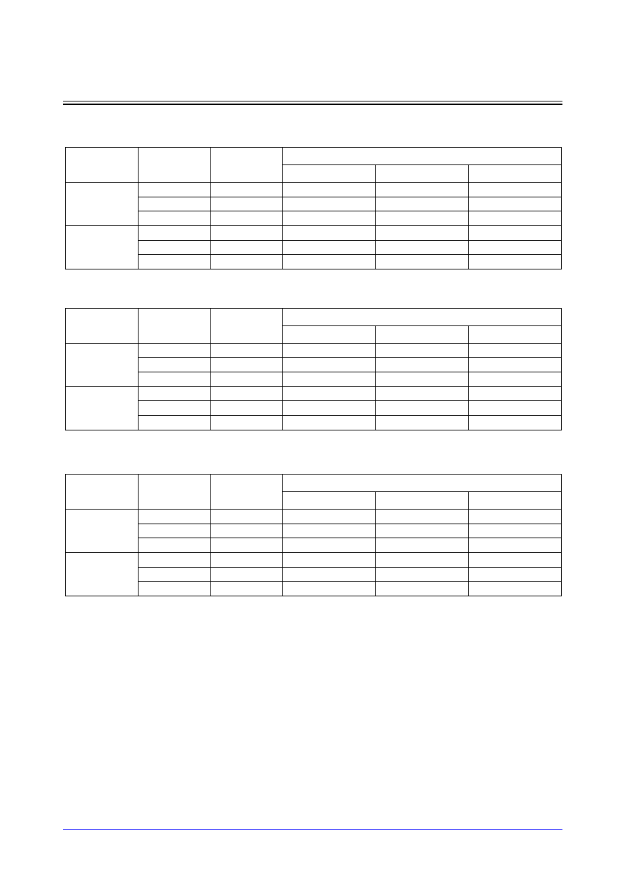
STDL130
4-50
Samsung ASIC
PvODyz_LP
Open Drain Output Buffers
Switching Characteristics
(Typical process, 25
∞
C, 1.8V, 2.5V, t
R
/t
F
=0.20ns, CL: Capacitive Load[pF])
PMOD4SM_LP
PMOD8SM_LP
PMOD12SM_LP
Path
Parameter
Delay [ns]
CL = 50.0pF
Delay Equations [ns]
Group1*
Group2*
Group3*
TN to PAD
tF
6.772
0.827 + 0.119*CL
0.758 + 0.120*CL
0.687 + 0.121*CL
tPHL
5.655
2.280 + 0.067*CL
2.337 + 0.066*CL
2.358 + 0.066*CL
tPLZ
1.046
1.045 + 0.000*CL
1.045 + 0.000*CL
1.045 + 0.000*CL
EN to PAD
tF
6.772
0.827 + 0.119*CL
0.758 + 0.120*CL
0.687 + 0.121*CL
tPHL
5.757
2.382 + 0.067*CL
2.439 + 0.066*CL
2.460 + 0.066*CL
tPLZ
1.120
1.119 + 0.000*CL
1.120 + 0.000*CL
1.120 + 0.000*CL
*Group1 : CL < 50, *Group2 : 50 CL
<
<
=
= 75, *Group3 : 75 < CL
Path
Parameter
Delay [ns]
CL = 50.0pF
Delay Equations [ns]
Group1*
Group2*
Group3*
TN to PAD
tF
3.945
1.031 + 0.058*CL
1.039 + 0.058*CL
1.006 + 0.059*CL
tPHL
4.654
2.700 + 0.039*CL
2.857 + 0.036*CL
2.970 + 0.034*CL
tPLZ
1.266
1.265 + 0.000*CL
1.265 + 0.000*CL
1.265 + 0.000*CL
EN to PAD
tF
3.945
1.031 + 0.058*CL
1.039 + 0.058*CL
1.006 + 0.059*CL
tPHL
4.756
2.802 + 0.039*CL
2.960 + 0.036*CL
3.073 + 0.034*CL
tPLZ
1.340
1.339 + 0.000*CL
1.340 + 0.000*CL
1.340 + 0.000*CL
*Group1 : CL < 50, *Group2 : 50 CL
<
<
=
= 75, *Group3 : 75 < CL
Path
Parameter
Delay [ns]
CL = 50.0pF
Delay Equations [ns]
Group1*
Group2*
Group3*
TN to PAD
tF
3.000
1.030 + 0.039*CL
1.075 + 0.039*CL
1.079 + 0.038*CL
tPHL
4.103
2.625 + 0.030*CL
2.794 + 0.026*CL
2.929 + 0.024*CL
tPLZ
1.410
1.409 + 0.000*CL
1.409 + 0.000*CL
1.410 + 0.000*CL
EN to PAD
tF
3.000
1.030 + 0.039*CL
1.075 + 0.039*CL
1.080 + 0.038*CL
tPHL
4.205
2.728 + 0.030*CL
2.897 + 0.026*CL
3.032 + 0.024*CL
tPLZ
1.484
1.483 + 0.000*CL
1.484 + 0.000*CL
1.484 + 0.000*CL
*Group1 : CL < 50, *Group2 : 50 CL
<
<
=
= 75, *Group3 : 75 < CL

Samsung ASIC
4-51
STDL130
PvODyz_LP
Open Drain Output Buffers
Switching Characteristics
(Typical process, 25
∞
C, 1.8V, 2.5V, t
R
/t
F
=0.20ns, CL: Capacitive Load[pF])
PMOD16SM_LP
PMOD20SM_LP
PMOD24SM_LP
Path
Parameter
Delay [ns]
CL = 50.0pF
Delay Equations [ns]
Group1*
Group2*
Group3*
TN to PAD
tF
2.740
1.168 + 0.031*CL
1.255 + 0.030*CL
1.309 + 0.029*CL
tPHL
4.229
2.886 + 0.027*CL
3.084 + 0.023*CL
3.253 + 0.021*CL
tPLZ
1.626
1.626 + 0.000*CL
1.626 + 0.000*CL
1.626 + 0.000*CL
EN to PAD
tF
2.740
1.168 + 0.031*CL
1.255 + 0.030*CL
1.308 + 0.029*CL
tPHL
4.332
2.988 + 0.027*CL
3.186 + 0.023*CL
3.355 + 0.021*CL
tPLZ
1.701
1.700 + 0.000*CL
1.701 + 0.000*CL
1.701 + 0.000*CL
*Group1 : CL < 50, *Group2 : 50 CL
<
<
=
= 75, *Group3 : 75 < CL
Path
Parameter
Delay [ns]
CL = 50.0pF
Delay Equations [ns]
Group1*
Group2*
Group3*
TN to PAD
tF
2.523
1.184 + 0.027*CL
1.285 + 0.025*CL
1.359 + 0.024*CL
tPHL
4.197
2.968 + 0.025*CL
3.168 + 0.021*CL
3.341 + 0.018*CL
tPLZ
1.641
1.640 + 0.000*CL
1.641 + 0.000*CL
1.641 + 0.000*CL
EN to PAD
tF
2.523
1.184 + 0.027*CL
1.285 + 0.025*CL
1.359 + 0.024*CL
tPHL
4.300
3.070 + 0.025*CL
3.270 + 0.021*CL
3.444 + 0.018*CL
tPLZ
1.716
1.715 + 0.000*CL
1.715 + 0.000*CL
1.716 + 0.000*CL
*Group1 : CL < 50, *Group2 : 50 CL
<
<
=
= 75, *Group3 : 75 < CL

STDL130
4-52
Samsung ASIC
PvODyz_LP
Open Drain Output Buffers
Switching Characteristics
(Typical process, 25
∞
C, 1.8V, 2.5V, t
R
/t
F
=0.20ns, CL: Capacitive Load[pF])
PMOD12SH_LP
PMOD16SH_LP
PMOD20SH_LP
PMOD24SH_LP
Path
Parameter
Delay [ns]
CL = 50.0pF
Delay Equations [ns]
Group1*
Group2*
Group3*
TN to PAD
tF
4.173
1.871 + 0.046*CL
2.110 + 0.041*CL
2.268 + 0.039*CL
tPHL
5.241
3.110 + 0.043*CL
3.488 + 0.035*CL
3.813 + 0.031*CL
tPLZ
1.715
1.714 + 0.000*CL
1.715 + 0.000*CL
1.715 + 0.000*CL
EN to PAD
tF
4.173
1.871 + 0.046*CL
2.110 + 0.041*CL
2.268 + 0.039*CL
tPHL
5.344
3.212 + 0.043*CL
3.591 + 0.035*CL
3.916 + 0.031*CL
tPLZ
1.790
1.789 + 0.000*CL
1.790 + 0.000*CL
1.789 + 0.000*CL
*Group1 : CL < 50, *Group2 : 50 CL
<
<
=
= 75, *Group3 : 75 < CL
Path
Parameter
Delay [ns]
CL = 50.0pF
Delay Equations [ns]
Group1*
Group2*
Group3*
TN to PAD
tF
3.100
1.085 + 0.040*CL
1.154 + 0.039*CL
1.189 + 0.038*CL
tPHL
4.235
2.706 + 0.031*CL
2.890 + 0.027*CL
3.046 + 0.025*CL
tPLZ
1.272
1.272 + 0.000*CL
1.272 + 0.000*CL
1.272 + 0.000*CL
EN to PAD
tF
3.100
1.085 + 0.040*CL
1.154 + 0.039*CL
1.189 + 0.038*CL
tPHL
4.338
2.809 + 0.031*CL
2.993 + 0.027*CL
3.149 + 0.025*CL
tPLZ
1.347
1.347 + 0.000*CL
1.347 + 0.000*CL
1.347 + 0.000*CL
*Group1 : CL < 50, *Group2 : 50 CL
<
<
=
= 75, *Group3 : 75 < CL
Path
Parameter
Delay [ns]
CL = 50.0pF
Delay Equations [ns]
Group1*
Group2*
Group3*
TN to PAD
tF
3.755
1.721 + 0.041*CL
2.084 + 0.033*CL
2.371 + 0.030*CL
tPHL
5.373
3.501 + 0.037*CL
3.833 + 0.031*CL
4.145 + 0.027*CL
tPLZ
2.156
2.155 + 0.000*CL
2.156 + 0.000*CL
2.155 + 0.000*CL
EN to PAD
tF
3.755
1.721 + 0.041*CL
2.084 + 0.033*CL
2.371 + 0.030*CL
tPHL
5.476
3.603 + 0.037*CL
3.936 + 0.031*CL
4.248 + 0.027*CL
tPLZ
2.231
2.230 + 0.000*CL
2.230 + 0.000*CL
2.231 + 0.000*CL
*Group1 : CL < 50, *Group2 : 50 CL
<
<
=
= 75, *Group3 : 75 < CL
Path
Parameter
Delay [ns]
CL = 50.0pF
Delay Equations [ns]
Group1*
Group2*
Group3*
TN to PAD
tF
3.443
1.285 + 0.043*CL
1.799 + 0.033*CL
2.200 + 0.028*CL
tPHL
4.333
2.574 + 0.035*CL
2.839 + 0.030*CL
3.151 + 0.026*CL
tPLZ
2.488
2.487 + 0.000*CL
2.488 + 0.000*CL
2.488 + 0.000*CL
EN to PAD
tF
3.443
1.285 + 0.043*CL
1.799 + 0.033*CL
2.200 + 0.028*CL
tPHL
4.436
2.677 + 0.035*CL
2.942 + 0.030*CL
3.254 + 0.026*CL
tPLZ
2.563
2.562 + 0.000*CL
2.562 + 0.000*CL
2.563 + 0.000*CL
*Group1 : CL < 50, *Group2 : 50 CL
<
<
=
= 75, *Group3 : 75 < CL
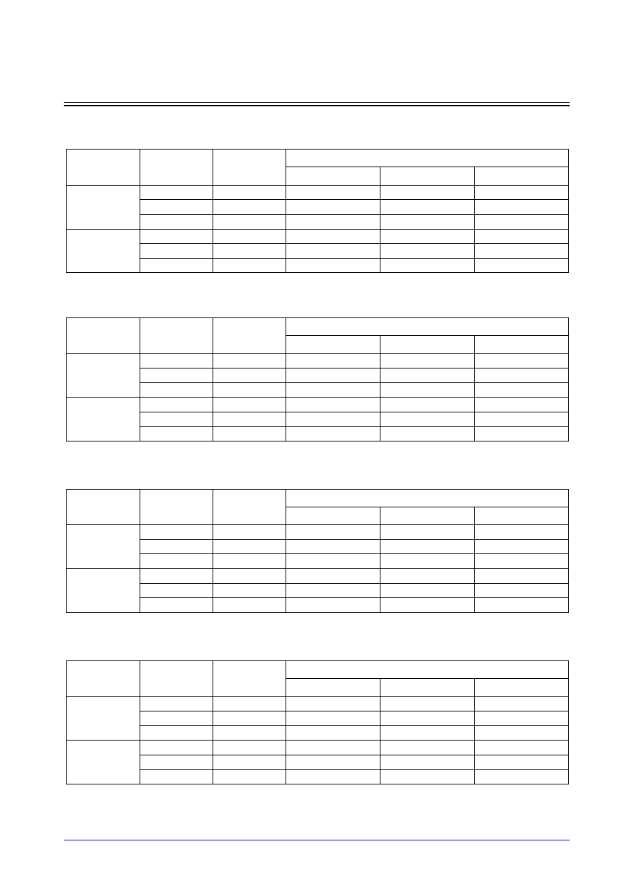
Samsung ASIC
4-53
STDL130
PvODyz_LP
Open Drain Output Buffers
Switching Characteristics
(Typical process, 25
∞
C, 1.8V, 3.3V, t
R
/t
F
=0.20ns, CL: Capacitive Load[pF])
PHOD1_LP
PHOD2_LP
PHOD4_LP
PHOD8_LP
Path
Parameter
Delay [ns]
CL = 50.0pF
Delay Equations [ns]
Group1*
Group2*
Group3*
TN to PAD
tF
26.612
1.552 + 0.501*CL
1.552 + 0.501*CL
1.546 + 0.501*CL
tPHL
13.674
1.724 + 0.239*CL
1.724 + 0.239*CL
1.724 + 0.239*CL
tPLZ
1.090
1.090 + 0.000*CL
1.090 + 0.000*CL
1.090 + 0.000*CL
EN to PAD
tF
26.612
1.552 + 0.501*CL
1.552 + 0.501*CL
1.546 + 0.501*CL
tPHL
13.777
1.826 + 0.239*CL
1.827 + 0.239*CL
1.827 + 0.239*CL
tPLZ
1.165
1.165 + 0.000*CL
1.165 + 0.000*CL
1.165 + 0.000*CL
*Group1 : CL < 50, *Group2 : 50 CL
<
<
=
= 75, *Group3 : 75 < CL
Path
Parameter
Delay [ns]
CL = 50.0pF
Delay Equations [ns]
Group1*
Group2*
Group3*
TN to PAD
tF
14.643
0.869 + 0.275*CL
0.865 + 0.276*CL
0.862 + 0.276*CL
tPHL
8.144
1.284 + 0.137*CL
1.283 + 0.137*CL
1.284 + 0.137*CL
tPLZ
0.886
0.886 + 0.000*CL
0.886 + 0.000*CL
0.886 + 0.000*CL
EN to PAD
tF
14.643
0.869 + 0.275*CL
0.865 + 0.276*CL
0.862 + 0.276*CL
tPHL
8.247
1.386 + 0.137*CL
1.386 + 0.137*CL
1.387 + 0.137*CL
tPLZ
0.961
0.961 + 0.000*CL
0.961 + 0.000*CL
0.961 + 0.000*CL
*Group1 : CL < 50, *Group2 : 50 CL
<
<
=
= 75, *Group3 : 75 < CL
Path
Parameter
Delay [ns]
CL = 50.0pF
Delay Equations [ns]
Group1*
Group2*
Group3*
TN to PAD
tF
8.642
0.523 + 0.162*CL
0.521 + 0.162*CL
0.516 + 0.162*CL
tPHL
5.362
1.055 + 0.086*CL
1.056 + 0.086*CL
1.056 + 0.086*CL
tPLZ
0.782
0.782 + 0.000*CL
0.782 + 0.000*CL
0.782 + 0.000*CL
EN to PAD
tF
8.642
0.523 + 0.162*CL
0.521 + 0.162*CL
0.516 + 0.162*CL
tPHL
5.464
1.157 + 0.086*CL
1.158 + 0.086*CL
1.158 + 0.086*CL
tPLZ
0.857
0.857 + 0.000*CL
0.856 + 0.000*CL
0.857 + 0.000*CL
*Group1 : CL < 50, *Group2 : 50 CL
<
<
=
= 75, *Group3 : 75 < CL
Path
Parameter
Delay [ns]
CL = 50.0pF
Delay Equations [ns]
Group1*
Group2*
Group3*
TN to PAD
tF
4.338
0.281 + 0.081*CL
0.280 + 0.081*CL
0.279 + 0.081*CL
tPHL
3.132
0.974 + 0.043*CL
0.977 + 0.043*CL
0.979 + 0.043*CL
tPLZ
0.888
0.888 + 0.000*CL
0.888 + 0.000*CL
0.888 + 0.000*CL
EN to PAD
tF
4.338
0.280 + 0.081*CL
0.280 + 0.081*CL
0.278 + 0.081*CL
tPHL
3.235
1.076 + 0.043*CL
1.080 + 0.043*CL
1.082 + 0.043*CL
tPLZ
0.963
0.963 + 0.000*CL
0.962 + 0.000*CL
0.963 + 0.000*CL
*Group1 : CL < 50, *Group2 : 50 CL
<
<
=
= 75, *Group3 : 75 < CL
STDL130
4-54
Samsung ASIC
PvODyz_LP
Open Drain Output Buffers
Switching Characteristics
(Typical process, 25
∞
C, 1.8V, 3.3V, t
R
/t
F
=0.20ns, CL: Capacitive Load[pF])
PHOD12_LP
PHOD16_LP
PHOD20_LP
PHOD24_LP
Path
Parameter
Delay [ns]
CL = 50.0pF
Delay Equations [ns]
Group1*
Group2*
Group3*
TN to PAD
tF
2.909
0.213 + 0.054*CL
0.207 + 0.054*CL
0.203 + 0.054*CL
tPHL
2.428
0.985 + 0.029*CL
0.989 + 0.029*CL
0.992 + 0.029*CL
tPLZ
0.993
0.993 + 0.000*CL
0.993 + 0.000*CL
0.993 + 0.000*CL
EN to PAD
tF
2.909
0.213 + 0.054*CL
0.207 + 0.054*CL
0.203 + 0.054*CL
tPHL
2.531
1.087 + 0.029*CL
1.092 + 0.029*CL
1.095 + 0.029*CL
tPLZ
1.068
1.068 + 0.000*CL
1.068 + 0.000*CL
1.068 + 0.000*CL
*Group1 : CL < 50, *Group2 : 50 CL
<
<
=
= 75, *Group3 : 75 < CL
Path
Parameter
Delay [ns]
CL = 50.0pF
Delay Equations [ns]
Group1*
Group2*
Group3*
TN to PAD
tF
2.190
0.175 + 0.040*CL
0.166 + 0.040*CL
0.160 + 0.041*CL
tPHL
2.063
0.979 + 0.022*CL
0.983 + 0.022*CL
0.985 + 0.022*CL
tPLZ
0.894
0.894 + 0.000*CL
0.894 + 0.000*CL
0.894 + 0.000*CL
EN to PAD
tF
2.190
0.175 + 0.040*CL
0.166 + 0.040*CL
0.160 + 0.041*CL
tPHL
2.166
1.082 + 0.022*CL
1.086 + 0.022*CL
1.089 + 0.022*CL
tPLZ
0.969
0.969 + 0.000*CL
0.969 + 0.000*CL
0.969 + 0.000*CL
*Group1 : CL < 50, *Group2 : 50 CL
<
<
=
= 75, *Group3 : 75 < CL
Path
Parameter
Delay [ns]
CL = 50.0pF
Delay Equations [ns]
Group1*
Group2*
Group3*
TN to PAD
tF
1.771
0.174 + 0.032*CL
0.160 + 0.032*CL
0.150 + 0.032*CL
tPHL
1.878
1.009 + 0.017*CL
1.013 + 0.017*CL
1.016 + 0.017*CL
tPLZ
0.945
0.945 + 0.000*CL
0.945 + 0.000*CL
0.945 + 0.000*CL
EN to PAD
tF
1.771
0.174 + 0.032*CL
0.161 + 0.032*CL
0.150 + 0.032*CL
tPHL
1.981
1.111 + 0.017*CL
1.116 + 0.017*CL
1.118 + 0.017*CL
tPLZ
1.020
1.020 + 0.000*CL
1.020 + 0.000*CL
1.020 + 0.000*CL
*Group1 : CL < 50, *Group2 : 50 CL
<
<
=
= 75, *Group3 : 75 < CL
Path
Parameter
Delay [ns]
CL = 50.0pF
Delay Equations [ns]
Group1*
Group2*
Group3*
TN to PAD
tF
1.500
0.184 + 0.026*CL
0.168 + 0.027*CL
0.154 + 0.027*CL
tPHL
1.770
1.040 + 0.015*CL
1.047 + 0.014*CL
1.050 + 0.014*CL
tPLZ
0.997
0.997 + 0.000*CL
0.997 + 0.000*CL
0.997 + 0.000*CL
EN to PAD
tF
1.500
0.184 + 0.026*CL
0.168 + 0.027*CL
0.154 + 0.027*CL
tPHL
1.873
1.143 + 0.015*CL
1.150 + 0.014*CL
1.153 + 0.014*CL
tPLZ
1.071
1.071 + 0.000*CL
1.071 + 0.000*CL
1.071 + 0.000*CL
*Group1 : CL < 50, *Group2 : 50 CL
<
<
=
= 75, *Group3 : 75 < CL
Samsung ASIC
4-55
STDL130
PvODyz_LP
Open Drain Output Buffers
Switching Characteristics
(Typical process, 25
∞
C, 1.8V, 3.3V, t
R
/t
F
=0.20ns, CL: Capacitive Load[pF])
PHOD4SM_LP
PHOD8SM_LP
PHOD12SM_LP
Path
Parameter
Delay [ns]
CL = 50.0pF
Delay Equations [ns]
Group1*
Group2*
Group3*
TN to PAD
tF
8.701
0.638 + 0.161*CL
0.610 + 0.162*CL
0.588 + 0.162*CL
tPHL
5.814
1.501 + 0.086*CL
1.508 + 0.086*CL
1.509 + 0.086*CL
tPLZ
0.762
0.762 + 0.000*CL
0.762 + 0.000*CL
0.762 + 0.000*CL
EN to PAD
tF
8.701
0.638 + 0.161*CL
0.610 + 0.162*CL
0.588 + 0.162*CL
tPHL
5.917
1.604 + 0.086*CL
1.611 + 0.086*CL
1.610 + 0.086*CL
tPLZ
0.837
0.837 + 0.000*CL
0.837 + 0.000*CL
0.837 + 0.000*CL
*Group1 : CL < 50, *Group2 : 50 CL
<
<
=
= 75, *Group3 : 75 < CL
Path
Parameter
Delay [ns]
CL = 50.0pF
Delay Equations [ns]
Group1*
Group2*
Group3*
TN to PAD
tF
4.465
0.504 + 0.079*CL
0.467 + 0.080*CL
0.431 + 0.080*CL
tPHL
3.793
1.601 + 0.044*CL
1.629 + 0.043*CL
1.642 + 0.043*CL
tPLZ
0.909
0.908 + 0.000*CL
0.908 + 0.000*CL
0.909 + 0.000*CL
EN to PAD
tF
4.465
0.504 + 0.079*CL
0.467 + 0.080*CL
0.431 + 0.080*CL
tPHL
3.896
1.704 + 0.044*CL
1.732 + 0.043*CL
1.744 + 0.043*CL
tPLZ
0.984
0.984 + 0.000*CL
0.984 + 0.000*CL
0.984 + 0.000*CL
*Group1 : CL < 50, *Group2 : 50 CL
<
<
=
= 75, *Group3 : 75 < CL
Path
Parameter
Delay [ns]
CL = 50.0pF
Delay Equations [ns]
Group1*
Group2*
Group3*
TN to PAD
tF
3.242
0.671 + 0.051*CL
0.652 + 0.052*CL
0.612 + 0.052*CL
tPHL
3.403
1.824 + 0.032*CL
1.909 + 0.030*CL
1.962 + 0.029*CL
tPLZ
1.086
1.086 + 0.000*CL
1.086 + 0.000*CL
1.086 + 0.000*CL
EN to PAD
tF
3.242
0.671 + 0.051*CL
0.652 + 0.052*CL
0.612 + 0.052*CL
tPHL
3.506
1.927 + 0.032*CL
2.012 + 0.030*CL
2.065 + 0.029*CL
tPLZ
1.161
1.161 + 0.000*CL
1.161 + 0.000*CL
1.161 + 0.000*CL
*Group1 : CL < 50, *Group2 : 50 CL
<
<
=
= 75, *Group3 : 75 < CL

STDL130
4-56
Samsung ASIC
PvODyz_LP
Open Drain Output Buffers
Switching Characteristics
(Typical process, 25
∞
C, 1.8V, 3.3V, t
R
/t
F
=0.20ns, CL: Capacitive Load[pF])
PHOD16SM_LP
PHOD20SM_LP
PHOD24SM_LP
Path
Parameter
Delay [ns]
CL = 50.0pF
Delay Equations [ns]
Group1*
Group2*
Group3*
TN to PAD
tF
2.770
0.849 + 0.038*CL
0.868 + 0.038*CL
0.852 + 0.038*CL
tPHL
3.313
1.958 + 0.027*CL
2.096 + 0.024*CL
2.199 + 0.023*CL
tPLZ
1.267
1.267 + 0.000*CL
1.267 + 0.000*CL
1.267 + 0.000*CL
EN to PAD
tF
2.770
0.848 + 0.038*CL
0.868 + 0.038*CL
0.852 + 0.038*CL
tPHL
3.416
2.061 + 0.027*CL
2.199 + 0.024*CL
2.301 + 0.023*CL
tPLZ
1.342
1.342 + 0.000*CL
1.342 + 0.000*CL
1.342 + 0.000*CL
*Group1 : CL < 50, *Group2 : 50 CL
<
<
=
= 75, *Group3 : 75 < CL
Path
Parameter
Delay [ns]
CL = 50.0pF
Delay Equations [ns]
Group1*
Group2*
Group3*
TN to PAD
tF
2.336
0.764 + 0.031*CL
0.798 + 0.031*CL
0.804 + 0.031*CL
tPHL
3.156
2.013 + 0.023*CL
2.138 + 0.020*CL
2.239 + 0.019*CL
tPLZ
1.262
1.262 + 0.000*CL
1.262 + 0.000*CL
1.262 + 0.000*CL
EN to PAD
tF
2.336
0.764 + 0.031*CL
0.798 + 0.031*CL
0.804 + 0.031*CL
tPHL
3.259
2.116 + 0.023*CL
2.241 + 0.020*CL
2.342 + 0.019*CL
tPLZ
1.337
1.337 + 0.000*CL
1.337 + 0.000*CL
1.337 + 0.000*CL
*Group1 : CL < 50, *Group2 : 50 CL
<
<
=
= 75, *Group3 : 75 < CL
Samsung ASIC
4-57
STDL130
PvODyz_LP
Open Drain Output Buffers
Switching Characteristics
(Typical process, 25
∞
C, 1.8V, 3.3V, t
R
/t
F
=0.20ns, CL: Capacitive Load[pF])
PHOD12SH_LP
PHOD16SH_LP
PHOD20SH_LP
PHOD24SH_LP
Path
Parameter
Delay [ns]
CL = 50.0pF
Delay Equations [ns]
Group1*
Group2*
Group3*
TN to PAD
tF
3.763
1.142 + 0.052*CL
1.192 + 0.051*CL
1.199 + 0.051*CL
tPHL
4.428
2.570 + 0.037*CL
2.760 + 0.033*CL
2.913 + 0.031*CL
tPLZ
1.273
1.272 + 0.000*CL
1.273 + 0.000*CL
1.272 + 0.000*CL
EN to PAD
tF
3.763
1.142 + 0.052*CL
1.192 + 0.051*CL
1.199 + 0.051*CL
tPHL
4.531
2.673 + 0.037*CL
2.863 + 0.033*CL
3.016 + 0.031*CL
tPLZ
1.347
1.347 + 0.000*CL
1.347 + 0.000*CL
1.347 + 0.000*CL
*Group1 : CL < 50, *Group2 : 50 CL
<
<
=
= 75, *Group3 : 75 < CL
Path
Parameter
Delay [ns]
CL = 50.0pF
Delay Equations [ns]
Group1*
Group2*
Group3*
TN to PAD
tF
3.100
1.085 + 0.040*CL
1.154 + 0.039*CL
1.189 + 0.038*CL
tPHL
4.235
2.706 + 0.031*CL
2.890 + 0.027*CL
3.046 + 0.025*CL
tPLZ
1.272
1.272 + 0.000*CL
1.272 + 0.000*CL
1.272 + 0.000*CL
EN to PAD
tF
3.100
1.085 + 0.040*CL
1.154 + 0.039*CL
1.189 + 0.038*CL
tPHL
4.338
2.809 + 0.031*CL
2.993 + 0.027*CL
3.149 + 0.025*CL
tPLZ
1.347
1.347 + 0.000*CL
1.347 + 0.000*CL
1.347 + 0.000*CL
*Group1 : CL < 50, *Group2 : 50 CL
<
<
=
= 75, *Group3 : 75 < CL
Path
Parameter
Delay [ns]
CL = 50.0pF
Delay Equations [ns]
Group1*
Group2*
Group3*
TN to PAD
tF
3.044
1.309 + 0.035*CL
1.418 + 0.033*CL
1.499 + 0.031*CL
tPHL
4.483
2.988 + 0.030*CL
3.210 + 0.025*CL
3.405 + 0.023*CL
tPLZ
1.513
1.513 + 0.000*CL
1.513 + 0.000*CL
1.513 + 0.000*CL
EN to PAD
tF
3.044
1.309 + 0.035*CL
1.418 + 0.033*CL
1.499 + 0.031*CL
tPHL
4.586
3.090 + 0.030*CL
3.313 + 0.025*CL
3.508 + 0.023*CL
tPLZ
1.588
1.588 + 0.000*CL
1.588 + 0.000*CL
1.588 + 0.000*CL
*Group1 : CL < 50, *Group2 : 50 CL
<
<
=
= 75, *Group3 : 75 < CL
Path
Parameter
Delay [ns]
CL = 50.0pF
Delay Equations [ns]
Group1*
Group2*
Group3*
TN to PAD
tF
3.122
1.518 + 0.032*CL
1.670 + 0.029*CL
1.789 + 0.027*CL
tPHL
4.667
3.141 + 0.031*CL
3.401 + 0.025*CL
3.633 + 0.022*CL
tPLZ
1.747
1.747 + 0.000*CL
1.747 + 0.000*CL
1.747 + 0.000*CL
EN to PAD
tF
3.122
1.518 + 0.032*CL
1.670 + 0.029*CL
1.789 + 0.027*CL
tPHL
4.770
3.244 + 0.031*CL
3.504 + 0.025*CL
3.735 + 0.022*CL
tPLZ
1.822
1.822 + 0.000*CL
1.822 + 0.000*CL
1.822 + 0.000*CL
*Group1 : CL < 50, *Group2 : 50 CL
<
<
=
= 75, *Group3 : 75 < CL

STDL130
4-58
Samsung ASIC
PvODyz_LP
Open Drain Output Buffers
Switching Characteristics
(Typical process, 25
∞
C, 1.8V, 3.3V, t
R
/t
F
=0.20ns, CL: Capacitive Load[pF])
PHTOD1_LP
PHTOD2_LP
PHTOD4_LP
PHTOD6_LP
Path
Parameter
Delay [ns]
CL = 50.0pF
Delay Equations [ns]
Group1*
Group2*
Group3*
TN to PAD
tF
28.071
4.173 + 0.478*CL
3.415 + 0.493*CL
3.040 + 0.498*CL
tPHL
14.822
3.137 + 0.234*CL
3.068 + 0.235*CL
2.909 + 0.237*CL
tPLZ
0.959
0.959 + 0.000*CL
0.959 + 0.000*CL
0.959 + 0.000*CL
EN to PAD
tF
28.071
4.173 + 0.478*CL
3.415 + 0.493*CL
3.040 + 0.498*CL
tPHL
14.925
3.237 + 0.234*CL
3.173 + 0.235*CL
3.008 + 0.237*CL
tPLZ
1.034
1.034 + 0.000*CL
1.034 + 0.000*CL
1.034 + 0.000*CL
*Group1 : CL < 50, *Group2 : 50 CL
<
<
=
= 75, *Group3 : 75 < CL
Path
Parameter
Delay [ns]
CL = 50.0pF
Delay Equations [ns]
Group1*
Group2*
Group3*
TN to PAD
tF
15.843
3.513 + 0.247*CL
2.661 + 0.264*CL
2.151 + 0.270*CL
tPHL
8.623
1.754 + 0.137*CL
1.833 + 0.136*CL
1.855 + 0.136*CL
tPLZ
0.753
0.753 + 0.000*CL
0.753 + 0.000*CL
0.753 + 0.000*CL
EN to PAD
tF
15.843
3.513 + 0.247*CL
2.661 + 0.264*CL
2.151 + 0.270*CL
tPHL
8.726
1.857 + 0.137*CL
1.935 + 0.136*CL
1.958 + 0.136*CL
tPLZ
0.829
0.829 + 0.000*CL
0.829 + 0.000*CL
0.829 + 0.000*CL
*Group1 : CL < 50, *Group2 : 50 CL
<
<
=
= 75, *Group3 : 75 < CL
Path
Parameter
Delay [ns]
CL = 50.0pF
Delay Equations [ns]
Group1*
Group2*
Group3*
TN to PAD
tF
8.616
2.928 + 0.114*CL
2.545 + 0.121*CL
1.976 + 0.129*CL
tPHL
5.267
1.768 + 0.070*CL
1.806 + 0.069*CL
1.844 + 0.069*CL
tPLZ
0.853
0.853 + 0.000*CL
0.853 + 0.000*CL
0.853 + 0.000*CL
EN to PAD
tF
8.616
2.928 + 0.114*CL
2.545 + 0.121*CL
1.976 + 0.129*CL
tPHL
5.370
1.870 + 0.070*CL
1.909 + 0.069*CL
1.946 + 0.069*CL
tPLZ
0.929
0.929 + 0.000*CL
0.929 + 0.000*CL
0.929 + 0.000*CL
*Group1 : CL < 50, *Group2 : 50 CL
<
<
=
= 75, *Group3 : 75 < CL
Path
Parameter
Delay [ns]
CL = 50.0pF
Delay Equations [ns]
Group1*
Group2*
Group3*
TN to PAD
tF
6.187
2.095 + 0.082*CL
2.217 + 0.079*CL
2.026 + 0.082*CL
tPHL
4.346
1.979 + 0.047*CL
2.019 + 0.047*CL
2.048 + 0.046*CL
tPLZ
0.958
0.958 + 0.000*CL
0.958 + 0.000*CL
0.958 + 0.000*CL
EN to PAD
tF
6.187
2.095 + 0.082*CL
2.217 + 0.079*CL
2.026 + 0.082*CL
tPHL
4.449
2.082 + 0.047*CL
2.122 + 0.047*CL
2.151 + 0.046*CL
tPLZ
1.033
1.033 + 0.000*CL
1.033 + 0.000*CL
1.033 + 0.000*CL
*Group1 : CL < 50, *Group2 : 50 CL
<
<
=
= 75, *Group3 : 75 < CL

Samsung ASIC
4-59
STDL130
PvODyz_LP
Open Drain Output Buffers
Switching Characteristics
(Typical process, 25
∞
C, 1.8V, 3.3V, t
R
/t
F
=0.20ns, CL: Capacitive Load[pF])
PHTOD4SM_LP
PHTOD6SM_LP
Path
Parameter
Delay [ns]
CL = 50.0pF
Delay Equations [ns]
Group1*
Group2*
Group3*
TN to PAD
tF
8.675
3.050 + 0.112*CL
2.638 + 0.121*CL
2.051 + 0.129*CL
tPHL
5.748
2.227 + 0.070*CL
2.281 + 0.069*CL
2.325 + 0.069*CL
tPLZ
0.902
0.902 + 0.000*CL
0.902 + 0.000*CL
0.902 + 0.000*CL
EN to PAD
tF
8.675
3.050 + 0.112*CL
2.638 + 0.121*CL
2.051 + 0.129*CL
tPHL
5.851
2.330 + 0.070*CL
2.384 + 0.069*CL
2.428 + 0.069*CL
tPLZ
0.977
0.977 + 0.000*CL
0.977 + 0.000*CL
0.977 + 0.000*CL
*Group1 : CL < 50, *Group2 : 50 CL
<
<
=
= 75, *Group3 : 75 < CL
Path
Parameter
Delay [ns]
CL = 50.0pF
Delay Equations [ns]
Group1*
Group2*
Group3*
TN to PAD
tF
6.516
2.660 + 0.077*CL
2.711 + 0.076*CL
2.440 + 0.080*CL
tPHL
5.198
2.704 + 0.050*CL
2.813 + 0.048*CL
2.888 + 0.047*CL
tPLZ
1.079
1.079 + 0.000*CL
1.079 + 0.000*CL
1.079 + 0.000*CL
EN to PAD
tF
6.516
2.660 + 0.077*CL
2.711 + 0.076*CL
2.440 + 0.080*CL
tPHL
5.301
2.808 + 0.050*CL
2.916 + 0.048*CL
2.990 + 0.047*CL
tPLZ
1.154
1.154 + 0.000*CL
1.154 + 0.000*CL
1.154 + 0.000*CL
*Group1 : CL < 50, *Group2 : 50 CL
<
<
=
= 75, *Group3 : 75 < CL
STDL130
4-60
Samsung ASIC
PvOTyz_LP
Tri-State Output Buffers
Cell Availability
Logic Symbol
Standard Load (SL)
1.8V Interface
1.8V Interface
POT(1/2/4/8/12/16/20/24)_LP
POT(4/8/12/16/20/24)SM_LP
POT(12/16/20/24)SH_LP
3.3V-Tolerant
PTOT(1/2/4/6)_LP
PTOT(4/6)SM_LP
2.5V Interface
2.5V Interface
PMOT(1/2/4/8/12/16/20/24)_LP
PMOT(4/8/12/16/20/24)SM_LP
PMOT(12/16/20/24)SH_LP
3.3V Interface
3.3V Interface
PHOT(1/2/4/8/12/16/20/24)_LP
PHOT(4/8/12/16/20/24)SM_LP
PHOT(12/16/20/24)SH_LP
5V-Tolerant
PHTOT(1/2/4/6)_LP
PHTOT(4/6)SM_LP
Cell Name
TN
EN
A
POT(1/2/4/8/12/16/20/24)_LP
3.80
3.69
3.67
POT(4/8/12/16/20/24)SM_LP
3.80
3.69
3.67
POT(12/16/20/24)SH_LP
3.80
3.69
3.67
PTOT(1/2/4/6)_LP
3.80
3.69
3.67
PTOT(4/6)SM_LP
3.80
3.69
3.67
PMOT(1/2/4/8/12/16/20/24)_LP
3.74
3.64
6.31
PMOT(4/8/12/16/20/24)SM_LP
3.74
3.64
6.31
PMOT(12/16/20/24)SH_LP
3.74
3.64
6.31
PHOT(1/2/4/8/12/16/20/24)_LP
3.74
3.64
7.49
PHOT(4/8/12/16/20/24)SM_LP
3.74
3.64
7.49
PHOT(12/16/20/24)SH_LP
3.74
3.64
7.49
PHTOT(1/2/4/6)_LP
3.74
3.64
7.49
PHTOT(4/6)SM_LP
3.74
3.64
7.49
Truth Table
TN
EN
A
PAD
1
0
0
0
1
0
1
1
x
1
x
Hi-Z
0
x
x
Hi-Z
PAD
A
TN
EN

Samsung ASIC
4-61
STDL130
PvOTyz_LP
Tri-State Output Buffers
Switching Characteristics
(Typical process, 25
∞
C, 1.8V, t
R
/t
F
= 0.20ns, CL: Capacitive Load[pF])
POT1_LP
POT2_LP
Path
Parameter
Delay [ns]
CL = 50.0pF
Delay Equations [ns]
Group1*
Group2*
Group3*
A to PAD
tR
20.443
1.560 + 0.378*CL
1.557 + 0.378*CL
1.554 + 0.378*CL
tF
23.041
1.821 + 0.424*CL
1.811 + 0.425*CL
1.811 + 0.425*CL
tPLH
10.016
1.101 + 0.178*CL
1.102 + 0.178*CL
1.102 + 0.178*CL
tPHL
12.567
1.701 + 0.217*CL
1.699 + 0.217*CL
1.702 + 0.217*CL
TN to PAD
tR
20.443
1.560 + 0.378*CL
1.557 + 0.378*CL
1.554 + 0.378*CL
tF
23.041
1.821 + 0.424*CL
1.811 + 0.425*CL
1.811 + 0.425*CL
tPLH
10.066
1.149 + 0.178*CL
1.150 + 0.178*CL
1.150 + 0.178*CL
tPHL
12.638
1.769 + 0.217*CL
1.772 + 0.217*CL
1.769 + 0.217*CL
tPLZ
0.670
0.670 + 0.000*CL
0.670 + 0.000*CL
0.670 + 0.000*CL
tPHZ
0.531
0.531 + 0.000*CL
0.531 + 0.000*CL
0.531 + 0.000*CL
EN to PAD
tR
20.443
1.560 + 0.378*CL
1.557 + 0.378*CL
1.554 + 0.378*CL
tF
23.041
1.821 + 0.424*CL
1.811 + 0.425*CL
1.811 + 0.425*CL
tPLH
10.131
1.215 + 0.178*CL
1.215 + 0.178*CL
1.215 + 0.178*CL
tPHL
12.703
1.835 + 0.217*CL
1.837 + 0.217*CL
1.834 + 0.217*CL
tPLZ
0.704
0.704 + 0.000*CL
0.704 + 0.000*CL
0.704 + 0.000*CL
tPHZ
0.565
0.565 + 0.000*CL
0.564 + 0.000*CL
0.565 + 0.000*CL
*Group1 : CL < 50, *Group2 : 50 CL
<
<
=
= 75, *Group3 : 75 < CL
Path
Parameter
Delay [ns]
CL = 50.0pF
Delay Equations [ns]
Group1*
Group2*
Group3*
A to PAD
tR
13.759
1.082 + 0.254*CL
1.081 + 0.254*CL
1.078 + 0.254*CL
tF
12.208
0.976 + 0.225*CL
0.968 + 0.225*CL
0.962 + 0.225*CL
tPLH
7.049
0.980 + 0.121*CL
0.981 + 0.121*CL
0.984 + 0.121*CL
tPHL
6.904
1.052 + 0.117*CL
1.053 + 0.117*CL
1.053 + 0.117*CL
TN to PAD
tR
13.759
1.082 + 0.254*CL
1.081 + 0.254*CL
1.078 + 0.254*CL
tF
12.208
0.976 + 0.225*CL
0.968 + 0.225*CL
0.962 + 0.225*CL
tPLH
7.099
1.029 + 0.121*CL
1.030 + 0.121*CL
1.032 + 0.121*CL
tPHL
6.974
1.121 + 0.117*CL
1.122 + 0.117*CL
1.123 + 0.117*CL
tPLZ
0.511
0.511 + 0.000*CL
0.511 + 0.000*CL
0.511 + 0.000*CL
tPHZ
0.824
0.824 + 0.000*CL
0.824 + 0.000*CL
0.824 + 0.000*CL
EN to PAD
tR
13.759
1.082 + 0.254*CL
1.081 + 0.254*CL
1.078 + 0.254*CL
tF
12.208
0.976 + 0.225*CL
0.968 + 0.225*CL
0.962 + 0.225*CL
tPLH
7.165
1.095 + 0.121*CL
1.096 + 0.121*CL
1.097 + 0.121*CL
tPHL
7.039
1.186 + 0.117*CL
1.187 + 0.117*CL
1.188 + 0.117*CL
tPLZ
0.545
0.545 + 0.000*CL
0.545 + 0.000*CL
0.545 + 0.000*CL
tPHZ
0.858
0.858 + 0.000*CL
0.858 + 0.000*CL
0.858 + 0.000*CL
*Group1 : CL < 50, *Group2 : 50 CL
<
<
=
= 75, *Group3 : 75 < CL

STDL130
4-62
Samsung ASIC
PvOTyz_LP
Tri-State Output Buffers
Switching Characteristics
(Typical process, 25
∞
C, 1.8V, t
R
/t
F
= 0.20ns, CL: Capacitive Load[pF])
POT4_LP
POT8_LP
Path
Parameter
Delay [ns]
CL = 50.0pF
Delay Equations [ns]
Group1*
Group2*
Group3*
A to PAD
tR
6.856
0.564 + 0.126*CL
0.563 + 0.126*CL
0.562 + 0.126*CL
tF
6.905
0.572 + 0.127*CL
0.570 + 0.127*CL
0.562 + 0.127*CL
tPLH
3.694
0.719 + 0.059*CL
0.721 + 0.059*CL
0.723 + 0.059*CL
tPHL
4.142
0.727 + 0.068*CL
0.729 + 0.068*CL
0.729 + 0.068*CL
TN to PAD
tR
6.856
0.564 + 0.126*CL
0.563 + 0.126*CL
0.562 + 0.126*CL
tF
6.905
0.572 + 0.127*CL
0.570 + 0.127*CL
0.562 + 0.127*CL
tPLH
3.744
0.768 + 0.060*CL
0.771 + 0.059*CL
0.773 + 0.059*CL
tPHL
4.209
0.790 + 0.068*CL
0.794 + 0.068*CL
0.795 + 0.068*CL
tPLZ
0.428
0.428 + 0.000*CL
0.428 + 0.000*CL
0.428 + 0.000*CL
tPHZ
0.832
0.832 + 0.000*CL
0.832 + 0.000*CL
0.832 + 0.000*CL
EN to PAD
tR
6.856
0.564 + 0.126*CL
0.563 + 0.126*CL
0.562 + 0.126*CL
tF
6.905
0.572 + 0.127*CL
0.570 + 0.127*CL
0.562 + 0.127*CL
tPLH
3.810
0.833 + 0.060*CL
0.837 + 0.059*CL
0.838 + 0.059*CL
tPHL
4.275
0.855 + 0.068*CL
0.860 + 0.068*CL
0.861 + 0.068*CL
tPLZ
0.463
0.463 + 0.000*CL
0.463 + 0.000*CL
0.463 + 0.000*CL
tPHZ
0.866
0.866 + 0.000*CL
0.866 + 0.000*CL
0.866 + 0.000*CL
*Group1 : CL < 50, *Group2 : 50 CL
<
<
=
= 75, *Group3 : 75 < CL
Path
Parameter
Delay [ns]
CL = 50.0pF
Delay Equations [ns]
Group1*
Group2*
Group3*
A to PAD
tR
3.439
0.293 + 0.063*CL
0.292 + 0.063*CL
0.292 + 0.063*CL
tF
3.462
0.296 + 0.063*CL
0.294 + 0.063*CL
0.293 + 0.063*CL
tPLH
2.135
0.646 + 0.030*CL
0.648 + 0.030*CL
0.649 + 0.030*CL
tPHL
2.308
0.603 + 0.034*CL
0.603 + 0.034*CL
0.603 + 0.034*CL
TN to PAD
tR
3.439
0.293 + 0.063*CL
0.292 + 0.063*CL
0.292 + 0.063*CL
tF
3.462
0.293 + 0.063*CL
0.293 + 0.063*CL
0.293 + 0.063*CL
tPLH
2.186
0.695 + 0.030*CL
0.698 + 0.030*CL
0.699 + 0.030*CL
tPHL
2.371
0.657 + 0.034*CL
0.661 + 0.034*CL
0.664 + 0.034*CL
tPLZ
0.460
0.460 + 0.000*CL
0.460 + 0.000*CL
0.460 + 0.000*CL
tPHZ
0.876
0.876 + 0.000*CL
0.876 + 0.000*CL
0.876 + 0.000*CL
EN to PAD
tR
3.439
0.293 + 0.063*CL
0.292 + 0.063*CL
0.292 + 0.063*CL
tF
3.462
0.293 + 0.063*CL
0.293 + 0.063*CL
0.293 + 0.063*CL
tPLH
2.251
0.761 + 0.030*CL
0.763 + 0.030*CL
0.765 + 0.030*CL
tPHL
2.437
0.722 + 0.034*CL
0.727 + 0.034*CL
0.729 + 0.034*CL
tPLZ
0.495
0.495 + 0.000*CL
0.495 + 0.000*CL
0.495 + 0.000*CL
tPHZ
0.910
0.910 + 0.000*CL
0.910 + 0.000*CL
0.910 + 0.000*CL
*Group1 : CL < 50, *Group2 : 50 CL
<
<
=
= 75, *Group3 : 75 < CL

Samsung ASIC
4-63
STDL130
PvOTyz_LP
Tri-State Output Buffers
Switching Characteristics
(Typical process, 25
∞
C, 1.8V, t
R
/t
F
= 0.20ns, CL: Capacitive Load[pF])
POT12_LP
POT16_LP
Path
Parameter
Delay [ns]
CL = 50.0pF
Delay Equations [ns]
Group1*
Group2*
Group3*
A to PAD
tR
2.312
0.227 + 0.042*CL
0.218 + 0.042*CL
0.213 + 0.042*CL
tF
2.327
0.236 + 0.042*CL
0.219 + 0.042*CL
0.215 + 0.042*CL
tPLH
1.688
0.694 + 0.020*CL
0.696 + 0.020*CL
0.697 + 0.020*CL
tPHL
1.761
0.634 + 0.023*CL
0.628 + 0.023*CL
0.625 + 0.023*CL
TN to PAD
tR
2.312
0.228 + 0.042*CL
0.218 + 0.042*CL
0.213 + 0.042*CL
tF
2.324
0.218 + 0.042*CL
0.214 + 0.042*CL
0.211 + 0.042*CL
tPLH
1.739
0.743 + 0.020*CL
0.745 + 0.020*CL
0.747 + 0.020*CL
tPHL
1.812
0.664 + 0.023*CL
0.669 + 0.023*CL
0.672 + 0.023*CL
tPLZ
0.503
0.503 + 0.000*CL
0.503 + 0.000*CL
0.503 + 0.000*CL
tPHZ
1.097
1.096 + 0.000*CL
1.096 + 0.000*CL
1.097 + 0.000*CL
EN to PAD
tR
2.312
0.228 + 0.042*CL
0.218 + 0.042*CL
0.213 + 0.042*CL
tF
2.324
0.218 + 0.042*CL
0.214 + 0.042*CL
0.211 + 0.042*CL
tPLH
1.804
0.809 + 0.020*CL
0.811 + 0.020*CL
0.813 + 0.020*CL
tPHL
1.877
0.730 + 0.023*CL
0.734 + 0.023*CL
0.738 + 0.023*CL
tPLZ
0.537
0.537 + 0.000*CL
0.537 + 0.000*CL
0.537 + 0.000*CL
tPHZ
1.131
1.130 + 0.000*CL
1.130 + 0.000*CL
1.131 + 0.000*CL
*Group1 : CL < 50, *Group2 : 50 CL
<
<
=
= 75, *Group3 : 75 < CL
Path
Parameter
Delay [ns]
CL = 50.0pF
Delay Equations [ns]
Group1*
Group2*
Group3*
A to PAD
tR
1.762
0.220 + 0.031*CL
0.204 + 0.031*CL
0.192 + 0.031*CL
tF
1.777
0.248 + 0.031*CL
0.217 + 0.031*CL
0.194 + 0.031*CL
tPLH
1.508
0.759 + 0.015*CL
0.762 + 0.015*CL
0.764 + 0.015*CL
tPHL
1.528
0.698 + 0.017*CL
0.687 + 0.017*CL
0.679 + 0.017*CL
TN to PAD
tR
1.762
0.221 + 0.031*CL
0.203 + 0.031*CL
0.191 + 0.031*CL
tF
1.764
0.198 + 0.031*CL
0.188 + 0.032*CL
0.181 + 0.032*CL
tPLH
1.558
0.808 + 0.015*CL
0.812 + 0.015*CL
0.814 + 0.015*CL
tPHL
1.561
0.696 + 0.017*CL
0.701 + 0.017*CL
0.705 + 0.017*CL
tPLZ
0.544
0.544 + 0.000*CL
0.544 + 0.000*CL
0.544 + 0.000*CL
tPHZ
1.316
1.316 + 0.000*CL
1.316 + 0.000*CL
1.316 + 0.000*CL
EN to PAD
tR
1.762
0.221 + 0.031*CL
0.203 + 0.031*CL
0.191 + 0.031*CL
tF
1.764
0.198 + 0.031*CL
0.188 + 0.032*CL
0.181 + 0.032*CL
tPLH
1.624
0.874 + 0.015*CL
0.878 + 0.015*CL
0.880 + 0.015*CL
tPHL
1.626
0.761 + 0.017*CL
0.766 + 0.017*CL
0.770 + 0.017*CL
tPLZ
0.578
0.578 + 0.000*CL
0.578 + 0.000*CL
0.578 + 0.000*CL
tPHZ
1.350
1.350 + 0.000*CL
1.350 + 0.000*CL
1.350 + 0.000*CL
*Group1 : CL < 50, *Group2 : 50 CL
<
<
=
= 75, *Group3 : 75 < CL
STDL130
4-64
Samsung ASIC
PvOTyz_LP
Tri-State Output Buffers
Switching Characteristics
(Typical process, 25
∞
C, 1.8V, t
R
/t
F
= 0.20ns, CL: Capacitive Load[pF])
POT20_LP
POT24_LP
Path
Parameter
Delay [ns]
CL = 50.0pF
Delay Equations [ns]
Group1*
Group2*
Group3*
A to PAD
tR
1.448
0.237 + 0.024*CL
0.216 + 0.025*CL
0.199 + 0.025*CL
tF
1.470
0.290 + 0.024*CL
0.249 + 0.024*CL
0.219 + 0.025*CL
tPLH
1.434
0.827 + 0.012*CL
0.835 + 0.012*CL
0.838 + 0.012*CL
tPHL
1.425
0.780 + 0.013*CL
0.763 + 0.013*CL
0.751 + 0.013*CL
TN to PAD
tR
1.448
0.237 + 0.024*CL
0.216 + 0.025*CL
0.199 + 0.025*CL
tF
1.438
0.201 + 0.025*CL
0.188 + 0.025*CL
0.176 + 0.025*CL
tPLH
1.484
0.877 + 0.012*CL
0.885 + 0.012*CL
0.889 + 0.012*CL
tPHL
1.433
0.734 + 0.014*CL
0.742 + 0.014*CL
0.747 + 0.014*CL
tPLZ
0.585
0.585 + 0.000*CL
0.585 + 0.000*CL
0.585 + 0.000*CL
tPHZ
1.536
1.534 + 0.000*CL
1.535 + 0.000*CL
1.535 + 0.000*CL
EN to PAD
tR
1.448
0.237 + 0.024*CL
0.216 + 0.025*CL
0.199 + 0.025*CL
tF
1.438
0.201 + 0.025*CL
0.188 + 0.025*CL
0.176 + 0.025*CL
tPLH
1.550
0.942 + 0.012*CL
0.951 + 0.012*CL
0.954 + 0.012*CL
tPHL
1.498
0.800 + 0.014*CL
0.808 + 0.014*CL
0.813 + 0.014*CL
tPLZ
0.620
0.619 + 0.000*CL
0.619 + 0.000*CL
0.620 + 0.000*CL
tPHZ
1.569
1.569 + 0.000*CL
1.569 + 0.000*CL
1.569 + 0.000*CL
*Group1 : CL < 50, *Group2 : 50 CL
<
<
=
= 75, *Group3 : 75 < CL
Path
Parameter
Delay [ns]
CL = 50.0pF
Delay Equations [ns]
Group1*
Group2*
Group3*
A to PAD
tR
1.254
0.264 + 0.020*CL
0.243 + 0.020*CL
0.222 + 0.020*CL
tF
1.289
0.352 + 0.019*CL
0.300 + 0.020*CL
0.261 + 0.020*CL
tPLH
1.411
0.891 + 0.010*CL
0.907 + 0.010*CL
0.915 + 0.010*CL
tPHL
1.389
0.861 + 0.011*CL
0.851 + 0.011*CL
0.833 + 0.011*CL
TN to PAD
tR
1.254
0.263 + 0.020*CL
0.243 + 0.020*CL
0.222 + 0.020*CL
tF
1.232
0.214 + 0.020*CL
0.200 + 0.021*CL
0.187 + 0.021*CL
tPLH
1.462
0.940 + 0.010*CL
0.958 + 0.010*CL
0.965 + 0.010*CL
tPHL
1.366
0.772 + 0.012*CL
0.786 + 0.012*CL
0.794 + 0.012*CL
tPLZ
0.626
0.626 + 0.000*CL
0.626 + 0.000*CL
0.626 + 0.000*CL
tPHZ
1.754
1.753 + 0.000*CL
1.754 + 0.000*CL
1.754 + 0.000*CL
EN to PAD
tR
1.254
0.263 + 0.020*CL
0.243 + 0.020*CL
0.222 + 0.020*CL
tF
1.232
0.214 + 0.020*CL
0.200 + 0.021*CL
0.187 + 0.021*CL
tPLH
1.527
1.006 + 0.010*CL
1.023 + 0.010*CL
1.030 + 0.010*CL
tPHL
1.431
0.837 + 0.012*CL
0.851 + 0.012*CL
0.859 + 0.011*CL
tPLZ
0.660
0.660 + 0.000*CL
0.660 + 0.000*CL
0.660 + 0.000*CL
tPHZ
1.788
1.787 + 0.000*CL
1.788 + 0.000*CL
1.788 + 0.000*CL
*Group1 : CL < 50, *Group2 : 50 CL
<
<
=
= 75, *Group3 : 75 < CL

Samsung ASIC
4-65
STDL130
PvOTyz_LP
Tri-State Output Buffers
Switching Characteristics
(Typical process, 25
∞
C, 1.8V, t
R
/t
F
= 0.20ns, CL: Capacitive Load[pF])
POT4SM_LP
POT8SM_LP
Path
Parameter
Delay [ns]
CL = 50.0pF
Delay Equations [ns]
Group1*
Group2*
Group3*
A to PAD
tR
6.989
0.797 + 0.124*CL
0.748 + 0.125*CL
0.708 + 0.125*CL
tF
6.965
0.672 + 0.126*CL
0.654 + 0.126*CL
0.635 + 0.126*CL
tPLH
4.771
1.774 + 0.060*CL
1.791 + 0.060*CL
1.799 + 0.059*CL
tPHL
4.565
1.140 + 0.068*CL
1.150 + 0.068*CL
1.152 + 0.068*CL
TN to PAD
tR
6.989
0.797 + 0.124*CL
0.748 + 0.125*CL
0.708 + 0.125*CL
tF
6.965
0.672 + 0.126*CL
0.654 + 0.126*CL
0.635 + 0.126*CL
tPLH
4.820
1.821 + 0.060*CL
1.839 + 0.060*CL
1.848 + 0.060*CL
tPHL
4.632
1.201 + 0.069*CL
1.215 + 0.068*CL
1.218 + 0.068*CL
tPLZ
0.570
0.570 + 0.000*CL
0.570 + 0.000*CL
0.570 + 0.000*CL
tPHZ
1.165
1.164 + 0.000*CL
1.165 + 0.000*CL
1.164 + 0.000*CL
EN to PAD
tR
6.989
0.797 + 0.124*CL
0.748 + 0.125*CL
0.708 + 0.125*CL
tF
6.965
0.672 + 0.126*CL
0.654 + 0.126*CL
0.635 + 0.126*CL
tPLH
4.886
1.887 + 0.060*CL
1.905 + 0.060*CL
1.913 + 0.060*CL
tPHL
4.697
1.267 + 0.069*CL
1.280 + 0.068*CL
1.284 + 0.068*CL
tPLZ
0.604
0.604 + 0.000*CL
0.604 + 0.000*CL
0.604 + 0.000*CL
tPHZ
1.198
1.198 + 0.000*CL
1.198 + 0.000*CL
1.198 + 0.000*CL
*Group1 : CL < 50, *Group2 : 50 CL
<
<
=
= 75, *Group3 : 75 < CL
Path
Parameter
Delay [ns]
CL = 50.0pF
Delay Equations [ns]
Group1*
Group2*
Group3*
A to PAD
tR
3.901
0.914 + 0.060*CL
0.881 + 0.060*CL
0.833 + 0.061*CL
tF
3.917
0.903 + 0.060*CL
0.888 + 0.061*CL
0.842 + 0.061*CL
tPLH
3.941
2.299 + 0.033*CL
2.388 + 0.031*CL
2.442 + 0.030*CL
tPHL
3.987
2.105 + 0.038*CL
2.205 + 0.036*CL
2.271 + 0.035*CL
TN to PAD
tR
3.901
0.914 + 0.060*CL
0.881 + 0.060*CL
0.833 + 0.061*CL
tF
3.921
0.918 + 0.060*CL
0.895 + 0.061*CL
0.846 + 0.061*CL
tPLH
3.991
2.348 + 0.033*CL
2.437 + 0.031*CL
2.491 + 0.030*CL
tPHL
4.051
2.156 + 0.038*CL
2.264 + 0.036*CL
2.333 + 0.035*CL
tPLZ
0.742
0.742 + 0.000*CL
0.742 + 0.000*CL
0.742 + 0.000*CL
tPHZ
2.251
2.250 + 0.000*CL
2.250 + 0.000*CL
2.251 + 0.000*CL
EN to PAD
tR
3.901
0.914 + 0.060*CL
0.881 + 0.060*CL
0.833 + 0.061*CL
tF
3.921
0.918 + 0.060*CL
0.895 + 0.061*CL
0.846 + 0.061*CL
tPLH
4.056
2.413 + 0.033*CL
2.503 + 0.031*CL
2.557 + 0.030*CL
tPHL
4.117
2.222 + 0.038*CL
2.329 + 0.036*CL
2.398 + 0.035*CL
tPLZ
0.776
0.776 + 0.000*CL
0.776 + 0.000*CL
0.776 + 0.000*CL
tPHZ
2.284
2.284 + 0.000*CL
2.284 + 0.000*CL
2.284 + 0.000*CL
*Group1 : CL < 50, *Group2 : 50 CL
<
<
=
= 75, *Group3 : 75 < CL

STDL130
4-66
Samsung ASIC
PvOTyz_LP
Tri-State Output Buffers
Switching Characteristics
(Typical process, 25
∞
C, 1.8V, t
R
/t
F
= 0.20ns, CL: Capacitive Load[pF])
POT12SM_LP
POT16SM_LP
Path
Parameter
Delay [ns]
CL = 50.0pF
Delay Equations [ns]
Group1*
Group2*
Group3*
A to PAD
tR
3.488
1.433 + 0.041*CL
1.513 + 0.040*CL
1.541 + 0.039*CL
tF
3.463
1.345 + 0.042*CL
1.444 + 0.040*CL
1.503 + 0.040*CL
tPLH
4.229
2.711 + 0.030*CL
2.932 + 0.026*CL
3.113 + 0.024*CL
tPHL
4.244
2.618 + 0.033*CL
2.807 + 0.029*CL
2.980 + 0.026*CL
TN to PAD
tR
3.488
1.434 + 0.041*CL
1.514 + 0.039*CL
1.540 + 0.039*CL
tF
3.529
1.443 + 0.042*CL
1.550 + 0.040*CL
1.593 + 0.039*CL
tPLH
4.279
2.761 + 0.030*CL
2.982 + 0.026*CL
3.164 + 0.024*CL
tPHL
4.247
2.511 + 0.035*CL
2.763 + 0.030*CL
2.971 + 0.027*CL
tPLZ
1.015
1.015 + 0.000*CL
1.015 + 0.000*CL
1.015 + 0.000*CL
tPHZ
3.760
3.759 + 0.000*CL
3.760 + 0.000*CL
3.760 + 0.000*CL
EN to PAD
tR
3.488
1.434 + 0.041*CL
1.514 + 0.039*CL
1.541 + 0.039*CL
tF
3.529
1.443 + 0.042*CL
1.550 + 0.040*CL
1.593 + 0.039*CL
tPLH
4.345
2.826 + 0.030*CL
3.047 + 0.026*CL
3.230 + 0.024*CL
tPHL
4.312
2.576 + 0.035*CL
2.829 + 0.030*CL
3.037 + 0.027*CL
tPLZ
1.049
1.049 + 0.000*CL
1.049 + 0.000*CL
1.049 + 0.000*CL
tPHZ
3.794
3.793 + 0.000*CL
3.793 + 0.000*CL
3.794 + 0.000*CL
*Group1 : CL < 50, *Group2 : 50 CL
<
<
=
= 75, *Group3 : 75 < CL
Path
Parameter
Delay [ns]
CL = 50.0pF
Delay Equations [ns]
Group1*
Group2*
Group3*
A to PAD
tR
2.720
1.170 + 0.031*CL
1.226 + 0.030*CL
1.250 + 0.030*CL
tF
2.730
1.062 + 0.033*CL
1.168 + 0.031*CL
1.242 + 0.030*CL
tPLH
3.982
2.823 + 0.023*CL
2.989 + 0.020*CL
3.128 + 0.018*CL
tPHL
4.071
2.787 + 0.026*CL
2.941 + 0.023*CL
3.084 + 0.021*CL
TN to PAD
tR
2.720
1.169 + 0.031*CL
1.225 + 0.030*CL
1.250 + 0.030*CL
tF
2.779
1.170 + 0.032*CL
1.254 + 0.031*CL
1.302 + 0.030*CL
tPLH
4.033
2.874 + 0.023*CL
3.041 + 0.020*CL
3.179 + 0.018*CL
tPHL
4.099
2.750 + 0.027*CL
2.941 + 0.023*CL
3.104 + 0.021*CL
tPLZ
1.241
1.241 + 0.000*CL
1.241 + 0.000*CL
1.242 + 0.000*CL
tPHZ
3.727
3.725 + 0.000*CL
3.726 + 0.000*CL
3.727 + 0.000*CL
EN to PAD
tR
2.720
1.169 + 0.031*CL
1.226 + 0.030*CL
1.250 + 0.030*CL
tF
2.779
1.170 + 0.032*CL
1.254 + 0.031*CL
1.302 + 0.030*CL
tPLH
4.098
2.940 + 0.023*CL
3.106 + 0.020*CL
3.245 + 0.018*CL
tPHL
4.165
2.815 + 0.027*CL
3.006 + 0.023*CL
3.170 + 0.021*CL
tPLZ
1.275
1.275 + 0.000*CL
1.275 + 0.000*CL
1.275 + 0.000*CL
tPHZ
3.761
3.759 + 0.000*CL
3.760 + 0.000*CL
3.760 + 0.000*CL
*Group1 : CL < 50, *Group2 : 50 CL
<
<
=
= 75, *Group3 : 75 < CL

Samsung ASIC
4-67
STDL130
PvOTyz_LP
Tri-State Output Buffers
Switching Characteristics
(Typical process, 25
∞
C, 1.8V, t
R
/t
F
= 0.20ns, CL: Capacitive Load[pF])
POT20SM_LP
POT24SM_LP
Path
Parameter
Delay [ns]
CL = 50.0pF
Delay Equations [ns]
Group1*
Group2*
Group3*
A to PAD
tR
2.841
1.437 + 0.028*CL
1.554 + 0.026*CL
1.642 + 0.025*CL
tF
2.846
1.337 + 0.030*CL
1.465 + 0.028*CL
1.589 + 0.026*CL
tPLH
4.271
3.047 + 0.024*CL
3.259 + 0.020*CL
3.448 + 0.018*CL
tPHL
4.426
3.209 + 0.024*CL
3.334 + 0.022*CL
3.481 + 0.020*CL
TN to PAD
tR
2.840
1.435 + 0.028*CL
1.553 + 0.026*CL
1.642 + 0.025*CL
tF
2.943
1.419 + 0.030*CL
1.582 + 0.027*CL
1.710 + 0.026*CL
tPLH
4.324
3.098 + 0.025*CL
3.311 + 0.020*CL
3.499 + 0.018*CL
tPHL
4.330
2.882 + 0.029*CL
3.129 + 0.024*CL
3.354 + 0.021*CL
tPLZ
1.602
1.602 + 0.000*CL
1.602 + 0.000*CL
1.602 + 0.000*CL
tPHZ
5.221
5.219 + 0.000*CL
5.220 + 0.000*CL
5.221 + 0.000*CL
EN to PAD
tR
2.840
1.435 + 0.028*CL
1.553 + 0.026*CL
1.642 + 0.025*CL
tF
2.943
1.419 + 0.030*CL
1.582 + 0.027*CL
1.710 + 0.026*CL
tPLH
4.389
3.164 + 0.024*CL
3.376 + 0.020*CL
3.565 + 0.018*CL
tPHL
4.395
2.948 + 0.029*CL
3.195 + 0.024*CL
3.419 + 0.021*CL
tPLZ
1.636
1.636 + 0.000*CL
1.636 + 0.000*CL
1.636 + 0.000*CL
tPHZ
5.255
5.253 + 0.000*CL
5.254 + 0.000*CL
5.255 + 0.000*CL
*Group1 : CL < 50, *Group2 : 50 CL
<
<
=
= 75, *Group3 : 75 < CL
Path
Parameter
Delay [ns]
CL = 50.0pF
Delay Equations [ns]
Group1*
Group2*
Group3*
A to PAD
tR
2.631
1.444 + 0.024*CL
1.545 + 0.022*CL
1.624 + 0.021*CL
tF
2.487
1.185 + 0.026*CL
1.301 + 0.024*CL
1.416 + 0.022*CL
tPLH
4.554
3.443 + 0.022*CL
3.647 + 0.018*CL
3.827 + 0.016*CL
tPHL
4.563
3.505 + 0.021*CL
3.618 + 0.019*CL
3.753 + 0.017*CL
TN to PAD
tR
2.631
1.442 + 0.024*CL
1.543 + 0.022*CL
1.623 + 0.021*CL
tF
2.618
1.353 + 0.025*CL
1.481 + 0.023*CL
1.584 + 0.021*CL
tPLH
4.607
3.496 + 0.022*CL
3.700 + 0.018*CL
3.880 + 0.016*CL
tPHL
4.490
3.229 + 0.025*CL
3.452 + 0.021*CL
3.653 + 0.018*CL
tPLZ
1.602
1.602 + 0.000*CL
1.601 + 0.000*CL
1.602 + 0.000*CL
tPHZ
5.220
5.216 + 0.000*CL
5.218 + 0.000*CL
5.219 + 0.000*CL
EN to PAD
tR
2.631
1.442 + 0.024*CL
1.543 + 0.022*CL
1.623 + 0.021*CL
tF
2.618
1.353 + 0.025*CL
1.481 + 0.023*CL
1.584 + 0.021*CL
tPLH
4.672
3.562 + 0.022*CL
3.766 + 0.018*CL
3.946 + 0.016*CL
tPHL
4.555
3.294 + 0.025*CL
3.518 + 0.021*CL
3.718 + 0.018*CL
tPLZ
1.636
1.635 + 0.000*CL
1.636 + 0.000*CL
1.636 + 0.000*CL
tPHZ
5.253
5.250 + 0.000*CL
5.252 + 0.000*CL
5.253 + 0.000*CL
*Group1 : CL < 50, *Group2 : 50 CL
<
<
=
= 75, *Group3 : 75 < CL

STDL130
4-68
Samsung ASIC
PvOTyz_LP
Tri-State Output Buffers
Switching Characteristics
(Typical process, 25
∞
C, 1.8V, t
R
/t
F
= 0.20ns, CL: Capacitive Load[pF])
POT12SH_LP
POT16SH_LP
Path
Parameter
Delay [ns]
CL = 50.0pF
Delay Equations [ns]
Group1*
Group2*
Group3*
A to PAD
tR
4.452
2.140 + 0.046*CL
2.322 + 0.043*CL
2.456 + 0.041*CL
tF
4.667
2.239 + 0.049*CL
2.490 + 0.044*CL
2.673 + 0.041*CL
tPLH
6.150
4.215 + 0.039*CL
4.534 + 0.032*CL
4.819 + 0.029*CL
tPHL
6.602
4.305 + 0.046*CL
4.700 + 0.038*CL
5.054 + 0.033*CL
TN to PAD
tR
4.452
2.140 + 0.046*CL
2.323 + 0.043*CL
2.456 + 0.041*CL
tF
4.677
2.270 + 0.048*CL
2.507 + 0.043*CL
2.684 + 0.041*CL
tPLH
6.201
4.266 + 0.039*CL
4.586 + 0.032*CL
4.871 + 0.029*CL
tPHL
6.671
4.362 + 0.046*CL
4.764 + 0.038*CL
5.122 + 0.033*CL
tPLZ
1.461
1.461 + 0.000*CL
1.461 + 0.000*CL
1.461 + 0.000*CL
tPHZ
4.028
4.027 + 0.000*CL
4.028 + 0.000*CL
4.028 + 0.000*CL
EN to PAD
tR
4.452
2.140 + 0.046*CL
2.323 + 0.043*CL
2.456 + 0.041*CL
tF
4.677
2.269 + 0.048*CL
2.507 + 0.043*CL
2.684 + 0.041*CL
tPLH
6.267
4.332 + 0.039*CL
4.651 + 0.032*CL
4.936 + 0.029*CL
tPHL
6.736
4.428 + 0.046*CL
4.830 + 0.038*CL
5.187 + 0.033*CL
tPLZ
1.495
1.495 + 0.000*CL
1.495 + 0.000*CL
1.495 + 0.000*CL
tPHZ
4.062
4.061 + 0.000*CL
4.062 + 0.000*CL
4.062 + 0.000*CL
*Group1 : CL < 50, *Group2 : 50 CL
<
<
=
= 75, *Group3 : 75 < CL
Path
Parameter
Delay [ns]
CL = 50.0pF
Delay Equations [ns]
Group1*
Group2*
Group3*
A to PAD
tR
4.420
2.257 + 0.043*CL
2.554 + 0.037*CL
2.793 + 0.034*CL
tF
4.856
2.570 + 0.046*CL
2.960 + 0.038*CL
3.262 + 0.034*CL
tPLH
6.197
4.263 + 0.039*CL
4.607 + 0.032*CL
4.929 + 0.028*CL
tPHL
6.544
4.102 + 0.049*CL
4.601 + 0.039*CL
5.058 + 0.033*CL
TN to PAD
tR
4.421
2.257 + 0.043*CL
2.554 + 0.037*CL
2.794 + 0.034*CL
tF
4.859
2.575 + 0.046*CL
2.965 + 0.038*CL
3.266 + 0.034*CL
tPLH
6.248
4.313 + 0.039*CL
4.658 + 0.032*CL
4.980 + 0.028*CL
tPHL
6.620
4.179 + 0.049*CL
4.678 + 0.039*CL
5.135 + 0.033*CL
tPLZ
1.577
1.577 + 0.000*CL
1.577 + 0.000*CL
1.577 + 0.000*CL
tPHZ
2.417
2.416 + 0.000*CL
2.416 + 0.000*CL
2.417 + 0.000*CL
EN to PAD
tR
4.421
2.257 + 0.043*CL
2.554 + 0.037*CL
2.794 + 0.034*CL
tF
4.859
2.575 + 0.046*CL
2.965 + 0.038*CL
3.266 + 0.034*CL
tPLH
6.313
4.379 + 0.039*CL
4.724 + 0.032*CL
5.045 + 0.028*CL
tPHL
6.686
4.244 + 0.049*CL
4.744 + 0.039*CL
5.199 + 0.033*CL
tPLZ
1.611
1.611 + 0.000*CL
1.611 + 0.000*CL
1.611 + 0.000*CL
tPHZ
2.451
2.450 + 0.000*CL
2.450 + 0.000*CL
2.450 + 0.000*CL
*Group1 : CL < 50, *Group2 : 50 CL
<
<
=
= 75, *Group3 : 75 < CL

Samsung ASIC
4-69
STDL130
PvOTyz_LP
Tri-State Output Buffers
Switching Characteristics
(Typical process, 25
∞
C, 1.8V, t
R
/t
F
= 0.20ns, CL: Capacitive Load[pF])
POT20SH_LP
POT24SH_LP
Path
Parameter
Delay [ns]
CL = 50.0pF
Delay Equations [ns]
Group1*
Group2*
Group3*
A to PAD
tR
3.993
2.229 + 0.035*CL
2.478 + 0.030*CL
2.682 + 0.028*CL
tF
4.165
2.199 + 0.039*CL
2.489 + 0.034*CL
2.739 + 0.030*CL
tPLH
5.987
4.259 + 0.035*CL
4.594 + 0.028*CL
4.901 + 0.024*CL
tPHL
6.534
4.509 + 0.041*CL
4.890 + 0.033*CL
5.238 + 0.028*CL
TN to PAD
tR
3.994
2.230 + 0.035*CL
2.480 + 0.030*CL
2.683 + 0.028*CL
tF
4.167
2.201 + 0.039*CL
2.491 + 0.034*CL
2.741 + 0.030*CL
tPLH
6.039
4.311 + 0.035*CL
4.646 + 0.028*CL
4.954 + 0.024*CL
tPHL
6.611
4.587 + 0.040*CL
4.967 + 0.033*CL
5.315 + 0.028*CL
tPLZ
1.273
1.273 + 0.000*CL
1.273 + 0.000*CL
1.273 + 0.000*CL
tPHZ
3.132
3.131 + 0.000*CL
3.132 + 0.000*CL
3.132 + 0.000*CL
EN to PAD
tR
3.994
2.230 + 0.035*CL
2.480 + 0.030*CL
2.683 + 0.028*CL
tF
4.167
2.201 + 0.039*CL
2.491 + 0.034*CL
2.741 + 0.030*CL
tPLH
6.104
4.376 + 0.035*CL
4.712 + 0.028*CL
5.019 + 0.024*CL
tPHL
6.676
4.652 + 0.040*CL
5.033 + 0.033*CL
5.380 + 0.028*CL
tPLZ
1.307
1.307 + 0.000*CL
1.307 + 0.000*CL
1.307 + 0.000*CL
tPHZ
3.166
3.165 + 0.000*CL
3.165 + 0.000*CL
3.166 + 0.000*CL
*Group1 : CL < 50, *Group2 : 50 CL
<
<
=
= 75, *Group3 : 75 < CL
Path
Parameter
Delay [ns]
CL = 50.0pF
Delay Equations [ns]
Group1*
Group2*
Group3*
A to PAD
tR
3.868
2.138 + 0.035*CL
2.426 + 0.029*CL
2.665 + 0.026*CL
tF
4.135
2.247 + 0.038*CL
2.569 + 0.031*CL
2.844 + 0.028*CL
tPLH
5.905
4.250 + 0.033*CL
4.570 + 0.027*CL
4.864 + 0.023*CL
tPHL
6.558
4.552 + 0.040*CL
4.946 + 0.032*CL
5.306 + 0.027*CL
TN to PAD
tR
3.869
2.136 + 0.035*CL
2.426 + 0.029*CL
2.666 + 0.026*CL
tF
4.138
2.251 + 0.038*CL
2.572 + 0.031*CL
2.848 + 0.028*CL
tPLH
5.958
4.302 + 0.033*CL
4.623 + 0.027*CL
4.917 + 0.023*CL
tPHL
6.635
4.630 + 0.040*CL
5.024 + 0.032*CL
5.385 + 0.027*CL
tPLZ
1.541
1.541 + 0.000*CL
1.541 + 0.000*CL
1.542 + 0.000*CL
tPHZ
3.363
3.362 + 0.000*CL
3.362 + 0.000*CL
3.363 + 0.000*CL
EN to PAD
tR
3.869
2.136 + 0.035*CL
2.426 + 0.029*CL
2.666 + 0.026*CL
tF
4.138
2.251 + 0.038*CL
2.572 + 0.031*CL
2.848 + 0.028*CL
tPLH
6.023
4.368 + 0.033*CL
4.689 + 0.027*CL
4.982 + 0.023*CL
tPHL
6.700
4.696 + 0.040*CL
5.089 + 0.032*CL
5.450 + 0.027*CL
tPLZ
1.575
1.575 + 0.000*CL
1.575 + 0.000*CL
1.575 + 0.000*CL
tPHZ
3.397
3.395 + 0.000*CL
3.396 + 0.000*CL
3.397 + 0.000*CL
*Group1 : CL < 50, *Group2 : 50 CL
<
<
=
= 75, *Group3 : 75 < CL

STDL130
4-70
Samsung ASIC
PvOTyz_LP
Tri-State Output Buffers
Switching Characteristics
(Typical process, 25
∞
C, 1.8V, t
R
/t
F
= 0.20ns, CL: Capacitive Load[pF])
PTOT1_LP
PTOT2_LP
Path
Parameter
Delay [ns]
CL = 50.0pF
Delay Equations [ns]
Group1*
Group2*
Group3*
A to PAD
tR
22.581
2.531 + 0.401*CL
2.747 + 0.397*CL
2.927 + 0.394*CL
tF
25.239
4.211 + 0.421*CL
4.089 + 0.423*CL
3.984 + 0.424*CL
tPLH
11.246
2.109 + 0.183*CL
2.198 + 0.181*CL
2.273 + 0.180*CL
tPHL
13.028
1.839 + 0.224*CL
1.922 + 0.222*CL
2.003 + 0.221*CL
TN to PAD
tR
22.582
2.532 + 0.401*CL
2.748 + 0.397*CL
2.931 + 0.394*CL
tF
25.121
4.161 + 0.419*CL
4.013 + 0.422*CL
3.902 + 0.424*CL
tPLH
11.298
2.160 + 0.183*CL
2.250 + 0.181*CL
2.322 + 0.180*CL
tPHL
12.914
1.837 + 0.222*CL
1.886 + 0.221*CL
1.946 + 0.220*CL
tPLZ
0.591
0.591 + 0.000*CL
0.591 + 0.000*CL
0.591 + 0.000*CL
tPHZ
1.694
1.694 + 0.000*CL
1.694 + 0.000*CL
1.694 + 0.000*CL
EN to PAD
tR
22.582
2.532 + 0.401*CL
2.748 + 0.397*CL
2.931 + 0.394*CL
tF
25.121
4.161 + 0.419*CL
4.013 + 0.422*CL
3.902 + 0.424*CL
tPLH
11.364
2.225 + 0.183*CL
2.318 + 0.181*CL
2.387 + 0.180*CL
tPHL
12.979
1.903 + 0.222*CL
1.949 + 0.221*CL
2.015 + 0.220*CL
tPLZ
0.625
0.625 + 0.000*CL
0.625 + 0.000*CL
0.625 + 0.000*CL
tPHZ
1.728
1.728 + 0.000*CL
1.728 + 0.000*CL
1.728 + 0.000*CL
*Group1 : CL < 50, *Group2 : 50 CL
<
<
=
= 75, *Group3 : 75 < CL
Path
Parameter
Delay [ns]
CL = 50.0pF
Delay Equations [ns]
Group1*
Group2*
Group3*
A to PAD
tR
15.351
1.761 + 0.272*CL
1.937 + 0.268*CL
2.096 + 0.266*CL
tF
13.477
2.314 + 0.223*CL
2.249 + 0.225*CL
2.216 + 0.225*CL
tPLH
7.997
1.731 + 0.125*CL
1.799 + 0.124*CL
1.865 + 0.123*CL
tPHL
7.083
0.941 + 0.123*CL
1.054 + 0.121*CL
1.134 + 0.120*CL
TN to PAD
tR
15.352
1.760 + 0.272*CL
1.940 + 0.268*CL
2.096 + 0.266*CL
tF
13.363
2.264 + 0.222*CL
2.177 + 0.224*CL
2.135 + 0.224*CL
tPLH
8.048
1.780 + 0.125*CL
1.850 + 0.124*CL
1.916 + 0.123*CL
tPHL
6.984
0.933 + 0.121*CL
1.018 + 0.119*CL
1.085 + 0.118*CL
tPLZ
0.428
0.428 + 0.000*CL
0.428 + 0.000*CL
0.428 + 0.000*CL
tPHZ
2.394
2.395 + 0.000*CL
2.394 + 0.000*CL
2.394 + 0.000*CL
EN to PAD
tR
15.352
1.760 + 0.272*CL
1.940 + 0.268*CL
2.096 + 0.266*CL
tF
13.363
2.264 + 0.222*CL
2.177 + 0.224*CL
2.135 + 0.224*CL
tPLH
8.113
1.846 + 0.125*CL
1.916 + 0.124*CL
1.978 + 0.123*CL
tPHL
7.049
0.998 + 0.121*CL
1.083 + 0.119*CL
1.152 + 0.118*CL
tPLZ
0.463
0.463 + 0.000*CL
0.463 + 0.000*CL
0.463 + 0.000*CL
tPHZ
2.428
2.429 + 0.000*CL
2.428 + 0.000*CL
2.428 + 0.000*CL
*Group1 : CL < 50, *Group2 : 50 CL
<
<
=
= 75, *Group3 : 75 < CL

Samsung ASIC
4-71
STDL130
PvOTyz_LP
Tri-State Output Buffers
Switching Characteristics
(Typical process, 25
∞
C, 1.8V, t
R
/t
F
= 0.20ns, CL: Capacitive Load[pF])
PTOT4_LP
PTOT6_LP
Path
Parameter
Delay [ns]
CL = 50.0pF
Delay Equations [ns]
Group1*
Group2*
Group3*
A to PAD
tR
7.837
0.896 + 0.139*CL
1.012 + 0.137*CL
1.134 + 0.135*CL
tF
6.949
1.530 + 0.108*CL
1.396 + 0.111*CL
1.311 + 0.112*CL
tPLH
4.286
1.149 + 0.063*CL
1.189 + 0.062*CL
1.234 + 0.061*CL
tPHL
3.858
0.763 + 0.062*CL
0.800 + 0.061*CL
0.835 + 0.061*CL
TN to PAD
tR
7.838
0.898 + 0.139*CL
1.013 + 0.136*CL
1.134 + 0.135*CL
tF
6.853
1.488 + 0.107*CL
1.337 + 0.110*CL
1.241 + 0.112*CL
tPLH
4.337
1.198 + 0.063*CL
1.240 + 0.062*CL
1.285 + 0.061*CL
tPHL
3.801
0.784 + 0.060*CL
0.798 + 0.060*CL
0.818 + 0.060*CL
tPLZ
0.513
0.513 + 0.000*CL
0.513 + 0.000*CL
0.513 + 0.000*CL
tPHZ
2.389
2.391 + 0.000*CL
2.389 + 0.000*CL
2.388 + 0.000*CL
EN to PAD
tR
7.838
0.898 + 0.139*CL
1.013 + 0.136*CL
1.134 + 0.135*CL
tF
6.853
1.488 + 0.107*CL
1.337 + 0.110*CL
1.240 + 0.112*CL
tPLH
4.403
1.264 + 0.063*CL
1.305 + 0.062*CL
1.350 + 0.061*CL
tPHL
3.866
0.849 + 0.060*CL
0.864 + 0.060*CL
0.883 + 0.060*CL
tPLZ
0.547
0.547 + 0.000*CL
0.547 + 0.000*CL
0.547 + 0.000*CL
tPHZ
2.423
2.425 + 0.000*CL
2.423 + 0.000*CL
2.422 + 0.000*CL
*Group1 : CL < 50, *Group2 : 50 CL
<
<
=
= 75, *Group3 : 75 < CL
Path
Parameter
Delay [ns]
CL = 50.0pF
Delay Equations [ns]
Group1*
Group2*
Group3*
A to PAD
tR
5.502
0.676 + 0.097*CL
0.731 + 0.095*CL
0.803 + 0.094*CL
tF
4.700
1.065 + 0.073*CL
0.997 + 0.074*CL
0.928 + 0.075*CL
tPLH
3.443
1.253 + 0.044*CL
1.276 + 0.043*CL
1.303 + 0.043*CL
tPHL
2.900
0.825 + 0.042*CL
0.841 + 0.041*CL
0.862 + 0.041*CL
TN to PAD
tR
5.503
0.677 + 0.097*CL
0.732 + 0.095*CL
0.805 + 0.094*CL
tF
4.568
0.967 + 0.072*CL
0.894 + 0.073*CL
0.824 + 0.074*CL
tPLH
3.495
1.302 + 0.044*CL
1.327 + 0.043*CL
1.355 + 0.043*CL
tPHL
2.818
0.804 + 0.040*CL
0.811 + 0.040*CL
0.825 + 0.040*CL
tPLZ
0.595
0.596 + 0.000*CL
0.595 + 0.000*CL
0.595 + 0.000*CL
tPHZ
3.828
3.843 + 0.000*CL
3.828 + 0.000*CL
3.821 + 0.000*CL
EN to PAD
tR
5.503
0.677 + 0.097*CL
0.732 + 0.095*CL
0.805 + 0.094*CL
tF
4.568
0.968 + 0.072*CL
0.894 + 0.073*CL
0.824 + 0.074*CL
tPLH
3.560
1.368 + 0.044*CL
1.392 + 0.043*CL
1.420 + 0.043*CL
tPHL
2.883
0.869 + 0.040*CL
0.876 + 0.040*CL
0.891 + 0.040*CL
tPLZ
0.629
0.629 + 0.000*CL
0.629 + 0.000*CL
0.629 + 0.000*CL
tPHZ
3.862
3.877 + 0.000*CL
3.862 + 0.000*CL
3.856 + 0.000*CL
*Group1 : CL < 50, *Group2 : 50 CL
<
<
=
= 75, *Group3 : 75 < CL

STDL130
4-72
Samsung ASIC
PvOTyz_LP
Tri-State Output Buffers
Switching Characteristics
(Typical process, 25
∞
C, 1.8V, t
R
/t
F
= 0.20ns, CL: Capacitive Load[pF])
PTOT4SM_LP
PTOT6SM_LP
Path
Parameter
Delay [ns]
CL = 50.0pF
Delay Equations [ns]
Group1*
Group2*
Group3*
A to PAD
tR
8.104
1.346 + 0.135*CL
1.393 + 0.134*CL
1.448 + 0.133*CL
tF
7.598
2.488 + 0.102*CL
2.256 + 0.107*CL
2.060 + 0.109*CL
tPLH
5.561
2.395 + 0.063*CL
2.458 + 0.062*CL
2.510 + 0.061*CL
tPHL
5.504
2.314 + 0.064*CL
2.392 + 0.062*CL
2.447 + 0.061*CL
TN to PAD
tR
8.104
1.347 + 0.135*CL
1.393 + 0.134*CL
1.448 + 0.133*CL
tF
7.537
2.484 + 0.101*CL
2.235 + 0.106*CL
2.025 + 0.109*CL
tPLH
5.612
2.444 + 0.063*CL
2.509 + 0.062*CL
2.561 + 0.061*CL
tPHL
5.472
2.346 + 0.063*CL
2.405 + 0.061*CL
2.451 + 0.061*CL
tPLZ
0.531
0.531 + 0.000*CL
0.531 + 0.000*CL
0.531 + 0.000*CL
tPHZ
1.936
1.937 + 0.000*CL
1.936 + 0.000*CL
1.936 + 0.000*CL
EN to PAD
tR
8.104
1.347 + 0.135*CL
1.393 + 0.134*CL
1.448 + 0.133*CL
tF
7.537
2.484 + 0.101*CL
2.235 + 0.106*CL
2.025 + 0.109*CL
tPLH
5.677
2.510 + 0.063*CL
2.574 + 0.062*CL
2.626 + 0.061*CL
tPHL
5.538
2.411 + 0.063*CL
2.471 + 0.061*CL
2.516 + 0.061*CL
tPLZ
0.565
0.565 + 0.000*CL
0.565 + 0.000*CL
0.565 + 0.000*CL
tPHZ
1.970
1.971 + 0.000*CL
1.970 + 0.000*CL
1.970 + 0.000*CL
*Group1 : CL < 50, *Group2 : 50 CL
<
<
=
= 75, *Group3 : 75 < CL
Path
Parameter
Delay [ns]
CL = 50.0pF
Delay Equations [ns]
Group1*
Group2*
Group3*
A to PAD
tR
6.516
2.034 + 0.090*CL
2.024 + 0.090*CL
1.997 + 0.090*CL
tF
5.440
2.191 + 0.065*CL
2.045 + 0.068*CL
1.841 + 0.071*CL
tPLH
6.481
4.011 + 0.049*CL
4.189 + 0.046*CL
4.317 + 0.044*CL
tPHL
4.648
2.377 + 0.045*CL
2.500 + 0.043*CL
2.590 + 0.042*CL
TN to PAD
tR
6.516
2.033 + 0.090*CL
2.024 + 0.090*CL
1.997 + 0.090*CL
tF
5.392
2.214 + 0.064*CL
2.050 + 0.067*CL
1.832 + 0.070*CL
tPLH
6.533
4.062 + 0.049*CL
4.240 + 0.046*CL
4.369 + 0.044*CL
tPHL
4.591
2.372 + 0.044*CL
2.484 + 0.042*CL
2.571 + 0.041*CL
tPLZ
0.954
0.954 + 0.000*CL
0.954 + 0.000*CL
0.954 + 0.000*CL
tPHZ
2.404
2.410 + 0.000*CL
2.404 + 0.000*CL
2.403 + 0.000*CL
EN to PAD
tR
6.516
2.033 + 0.090*CL
2.024 + 0.090*CL
1.997 + 0.090*CL
tF
5.392
2.214 + 0.064*CL
2.050 + 0.067*CL
1.832 + 0.070*CL
tPLH
6.598
4.128 + 0.049*CL
4.306 + 0.046*CL
4.434 + 0.044*CL
tPHL
4.657
2.437 + 0.044*CL
2.549 + 0.042*CL
2.636 + 0.041*CL
tPLZ
0.988
0.988 + 0.000*CL
0.988 + 0.000*CL
0.988 + 0.000*CL
tPHZ
2.438
2.444 + 0.000*CL
2.438 + 0.000*CL
2.437 + 0.000*CL
*Group1 : CL < 50, *Group2 : 50 CL
<
<
=
= 75, *Group3 : 75 < CL

Samsung ASIC
4-73
STDL130
PvOTyz_LP
Tri-State Output Buffers
Switching Characteristics
(Typical process, 25
∞
C, 1.8V, 2.5V, t
R
/t
F
=0.20ns, CL: Capacitive Load[pF])
PMOT1_LP
PMOT2_LP
Path
Parameter
Delay [ns]
CL = 50.0pF
Delay Equations [ns]
Group1*
Group2*
Group3*
A to PAD
tR
26.043
1.408 + 0.493*CL
1.401 + 0.493*CL
1.398 + 0.493*CL
tF
22.782
1.225 + 0.431*CL
1.216 + 0.431*CL
1.213 + 0.431*CL
tPLH
13.279
1.406 + 0.237*CL
1.407 + 0.237*CL
1.410 + 0.237*CL
tPHL
12.586
1.449 + 0.223*CL
1.448 + 0.223*CL
1.448 + 0.223*CL
TN to PAD
tR
26.043
1.408 + 0.493*CL
1.401 + 0.493*CL
1.398 + 0.493*CL
tF
22.782
1.225 + 0.431*CL
1.216 + 0.431*CL
1.213 + 0.431*CL
tPLH
13.526
1.653 + 0.237*CL
1.652 + 0.237*CL
1.655 + 0.237*CL
tPHL
12.804
1.665 + 0.223*CL
1.664 + 0.223*CL
1.667 + 0.223*CL
tPLZ
1.013
1.013 + 0.000*CL
1.013 + 0.000*CL
1.013 + 0.000*CL
tPHZ
0.962
0.962 + 0.000*CL
0.962 + 0.000*CL
0.962 + 0.000*CL
EN to PAD
tR
26.043
1.408 + 0.493*CL
1.401 + 0.493*CL
1.398 + 0.493*CL
tF
22.782
1.225 + 0.431*CL
1.216 + 0.431*CL
1.213 + 0.431*CL
tPLH
13.632
1.759 + 0.237*CL
1.760 + 0.237*CL
1.760 + 0.237*CL
tPHL
12.910
1.771 + 0.223*CL
1.772 + 0.223*CL
1.772 + 0.223*CL
tPLZ
1.088
1.088 + 0.000*CL
1.088 + 0.000*CL
1.088 + 0.000*CL
tPHZ
1.037
1.037 + 0.000*CL
1.037 + 0.000*CL
1.037 + 0.000*CL
*Group1 : CL < 50, *Group2 : 50 CL
<
<
=
= 75, *Group3 : 75 < CL
Path
Parameter
Delay [ns]
CL = 50.0pF
Delay Equations [ns]
Group1*
Group2*
Group3*
A to PAD
tR
13.053
0.741 + 0.246*CL
0.737 + 0.246*CL
0.731 + 0.246*CL
tF
12.991
0.713 + 0.246*CL
0.707 + 0.246*CL
0.704 + 0.246*CL
tPLH
7.122
1.185 + 0.119*CL
1.187 + 0.119*CL
1.186 + 0.119*CL
tPHL
7.704
1.106 + 0.132*CL
1.105 + 0.132*CL
1.107 + 0.132*CL
TN to PAD
tR
13.053
0.741 + 0.246*CL
0.737 + 0.246*CL
0.731 + 0.246*CL
tF
12.991
0.713 + 0.246*CL
0.707 + 0.246*CL
0.704 + 0.246*CL
tPLH
7.370
1.430 + 0.119*CL
1.433 + 0.119*CL
1.431 + 0.119*CL
tPHL
7.920
1.319 + 0.132*CL
1.319 + 0.132*CL
1.321 + 0.132*CL
tPLZ
0.911
0.911 + 0.000*CL
0.911 + 0.000*CL
0.911 + 0.000*CL
tPHZ
1.115
1.115 + 0.000*CL
1.115 + 0.000*CL
1.115 + 0.000*CL
EN to PAD
tR
13.053
0.741 + 0.246*CL
0.737 + 0.246*CL
0.731 + 0.246*CL
tF
12.991
0.713 + 0.246*CL
0.707 + 0.246*CL
0.704 + 0.246*CL
tPLH
7.475
1.537 + 0.119*CL
1.538 + 0.119*CL
1.540 + 0.119*CL
tPHL
8.026
1.425 + 0.132*CL
1.426 + 0.132*CL
1.426 + 0.132*CL
tPLZ
0.986
0.986 + 0.000*CL
0.986 + 0.000*CL
0.986 + 0.000*CL
tPHZ
1.190
1.190 + 0.000*CL
1.190 + 0.000*CL
1.190 + 0.000*CL
*Group1 : CL < 50, *Group2 : 50 CL
<
<
=
= 75, *Group3 : 75 < CL

STDL130
4-74
Samsung ASIC
PvOTyz_LP
Tri-State Output Buffers
Switching Characteristics
(Typical process, 25
∞
C, 1.8V, 2.5V, t
R
/t
F
=0.20ns, CL: Capacitive Load[pF])
PMOT4_LP
PMOT8_LP
Path
Parameter
Delay [ns]
CL = 50.0pF
Delay Equations [ns]
Group1*
Group2*
Group3*
A to PAD
tR
6.568
0.423 + 0.123*CL
0.414 + 0.123*CL
0.409 + 0.123*CL
tF
6.518
0.386 + 0.123*CL
0.381 + 0.123*CL
0.378 + 0.123*CL
tPLH
4.194
1.220 + 0.059*CL
1.224 + 0.059*CL
1.226 + 0.059*CL
tPHL
4.298
1.005 + 0.066*CL
1.003 + 0.066*CL
1.000 + 0.066*CL
TN to PAD
tR
6.568
0.423 + 0.123*CL
0.414 + 0.123*CL
0.409 + 0.123*CL
tF
6.518
0.384 + 0.123*CL
0.381 + 0.123*CL
0.378 + 0.123*CL
tPLH
4.442
1.465 + 0.060*CL
1.471 + 0.059*CL
1.473 + 0.059*CL
tPHL
4.506
1.199 + 0.066*CL
1.204 + 0.066*CL
1.206 + 0.066*CL
tPLZ
1.016
1.016 + 0.000*CL
1.016 + 0.000*CL
1.016 + 0.000*CL
tPHZ
1.415
1.415 + 0.000*CL
1.415 + 0.000*CL
1.415 + 0.000*CL
EN to PAD
tR
6.568
0.423 + 0.123*CL
0.414 + 0.123*CL
0.409 + 0.123*CL
tF
6.518
0.384 + 0.123*CL
0.381 + 0.123*CL
0.378 + 0.123*CL
tPLH
4.547
1.572 + 0.060*CL
1.577 + 0.059*CL
1.579 + 0.059*CL
tPHL
4.611
1.305 + 0.066*CL
1.310 + 0.066*CL
1.311 + 0.066*CL
tPLZ
1.091
1.091 + 0.000*CL
1.091 + 0.000*CL
1.091 + 0.000*CL
tPHZ
1.490
1.490 + 0.000*CL
1.490 + 0.000*CL
1.490 + 0.000*CL
*Group1 : CL < 50, *Group2 : 50 CL
<
<
=
= 75, *Group3 : 75 < CL
Path
Parameter
Delay [ns]
CL = 50.0pF
Delay Equations [ns]
Group1*
Group2*
Group3*
A to PAD
tR
3.405
0.426 + 0.060*CL
0.379 + 0.061*CL
0.342 + 0.061*CL
tF
3.314
0.330 + 0.060*CL
0.279 + 0.061*CL
0.241 + 0.061*CL
tPLH
3.019
1.514 + 0.030*CL
1.527 + 0.030*CL
1.533 + 0.030*CL
tPHL
2.743
1.137 + 0.032*CL
1.117 + 0.033*CL
1.103 + 0.033*CL
TN to PAD
tR
3.405
0.426 + 0.060*CL
0.379 + 0.061*CL
0.341 + 0.061*CL
tF
3.299
0.249 + 0.061*CL
0.238 + 0.061*CL
0.231 + 0.061*CL
tPLH
3.266
1.760 + 0.030*CL
1.774 + 0.030*CL
1.781 + 0.030*CL
tPHL
2.902
1.236 + 0.033*CL
1.246 + 0.033*CL
1.251 + 0.033*CL
tPLZ
1.219
1.219 + 0.000*CL
1.219 + 0.000*CL
1.219 + 0.000*CL
tPHZ
2.009
2.009 + 0.000*CL
2.009 + 0.000*CL
2.009 + 0.000*CL
EN to PAD
tR
3.405
0.426 + 0.060*CL
0.379 + 0.061*CL
0.341 + 0.061*CL
tF
3.299
0.249 + 0.061*CL
0.238 + 0.061*CL
0.231 + 0.061*CL
tPLH
3.372
1.867 + 0.030*CL
1.880 + 0.030*CL
1.886 + 0.030*CL
tPHL
3.008
1.342 + 0.033*CL
1.351 + 0.033*CL
1.357 + 0.033*CL
tPLZ
1.294
1.294 + 0.000*CL
1.294 + 0.000*CL
1.294 + 0.000*CL
tPHZ
2.083
2.083 + 0.000*CL
2.083 + 0.000*CL
2.083 + 0.000*CL
*Group1 : CL < 50, *Group2 : 50 CL
<
<
=
= 75, *Group3 : 75 < CL

Samsung ASIC
4-75
STDL130
PvOTyz_LP
Tri-State Output Buffers
Switching Characteristics
(Typical process, 25
∞
C, 1.8V, 2.5V, t
R
/t
F
=0.20ns, CL: Capacitive Load[pF])
PMOT12_LP
PMOT16_LP
Path
Parameter
Delay [ns]
CL = 50.0pF
Delay Equations [ns]
Group1*
Group2*
Group3*
A to PAD
tR
2.290
0.316 + 0.039*CL
0.280 + 0.040*CL
0.251 + 0.041*CL
tF
2.280
0.361 + 0.038*CL
0.302 + 0.040*CL
0.256 + 0.040*CL
tPLH
2.376
1.370 + 0.020*CL
1.381 + 0.020*CL
1.385 + 0.020*CL
tPHL
2.296
1.266 + 0.021*CL
1.235 + 0.021*CL
1.213 + 0.022*CL
TN to PAD
tR
2.290
0.316 + 0.039*CL
0.280 + 0.040*CL
0.251 + 0.041*CL
tF
2.228
0.215 + 0.040*CL
0.198 + 0.041*CL
0.186 + 0.041*CL
tPLH
2.623
1.616 + 0.020*CL
1.628 + 0.020*CL
1.633 + 0.020*CL
tPHL
2.415
1.297 + 0.022*CL
1.306 + 0.022*CL
1.313 + 0.022*CL
tPLZ
1.168
1.168 + 0.000*CL
1.168 + 0.000*CL
1.168 + 0.000*CL
tPHZ
2.231
2.231 + 0.000*CL
2.231 + 0.000*CL
2.231 + 0.000*CL
EN to PAD
tR
2.290
0.316 + 0.039*CL
0.280 + 0.040*CL
0.251 + 0.041*CL
tF
2.228
0.215 + 0.040*CL
0.198 + 0.041*CL
0.186 + 0.041*CL
tPLH
2.729
1.722 + 0.020*CL
1.734 + 0.020*CL
1.738 + 0.020*CL
tPHL
2.521
1.404 + 0.022*CL
1.413 + 0.022*CL
1.419 + 0.022*CL
tPLZ
1.243
1.243 + 0.000*CL
1.243 + 0.000*CL
1.243 + 0.000*CL
tPHZ
2.306
2.306 + 0.000*CL
2.306 + 0.000*CL
2.306 + 0.000*CL
*Group1 : CL < 50, *Group2 : 50 CL
<
<
=
= 75, *Group3 : 75 < CL
Path
Parameter
Delay [ns]
CL = 50.0pF
Delay Equations [ns]
Group1*
Group2*
Group3*
A to PAD
tR
1.831
0.398 + 0.029*CL
0.361 + 0.029*CL
0.326 + 0.030*CL
tF
1.853
0.522 + 0.027*CL
0.434 + 0.028*CL
0.371 + 0.029*CL
tPLH
2.302
1.509 + 0.016*CL
1.544 + 0.015*CL
1.560 + 0.015*CL
tPHL
2.193
1.436 + 0.015*CL
1.433 + 0.015*CL
1.399 + 0.016*CL
TN to PAD
tR
1.831
0.397 + 0.029*CL
0.361 + 0.029*CL
0.325 + 0.030*CL
tF
1.725
0.242 + 0.030*CL
0.222 + 0.030*CL
0.204 + 0.030*CL
tPLH
2.550
1.756 + 0.016*CL
1.791 + 0.015*CL
1.807 + 0.015*CL
tPHL
2.227
1.372 + 0.017*CL
1.389 + 0.017*CL
1.398 + 0.017*CL
tPLZ
1.268
1.268 + 0.000*CL
1.268 + 0.000*CL
1.268 + 0.000*CL
tPHZ
2.670
2.670 + 0.000*CL
2.670 + 0.000*CL
2.670 + 0.000*CL
EN to PAD
tR
1.831
0.397 + 0.029*CL
0.361 + 0.029*CL
0.325 + 0.030*CL
tF
1.725
0.241 + 0.030*CL
0.222 + 0.030*CL
0.204 + 0.030*CL
tPLH
2.656
1.862 + 0.016*CL
1.897 + 0.015*CL
1.913 + 0.015*CL
tPHL
2.332
1.478 + 0.017*CL
1.495 + 0.017*CL
1.503 + 0.017*CL
tPLZ
1.343
1.343 + 0.000*CL
1.343 + 0.000*CL
1.343 + 0.000*CL
tPHZ
2.745
2.744 + 0.000*CL
2.745 + 0.000*CL
2.745 + 0.000*CL
*Group1 : CL < 50, *Group2 : 50 CL
<
<
=
= 75, *Group3 : 75 < CL
STDL130
4-76
Samsung ASIC
PvOTyz_LP
Tri-State Output Buffers
Switching Characteristics
(Typical process, 25
∞
C, 1.8V, 2.5V, t
R
/t
F
=0.20ns, CL: Capacitive Load[pF])
PMOT20_LP
PMOT24_LP
Path
Parameter
Delay [ns]
CL = 50.0pF
Delay Equations [ns]
Group1*
Group2*
Group3*
A to PAD
tR
1.600
0.479 + 0.022*CL
0.456 + 0.023*CL
0.421 + 0.023*CL
tF
1.674
0.739 + 0.019*CL
0.614 + 0.021*CL
0.525 + 0.022*CL
tPLH
2.318
1.623 + 0.014*CL
1.684 + 0.013*CL
1.720 + 0.012*CL
tPHL
2.205
1.562 + 0.013*CL
1.601 + 0.012*CL
1.607 + 0.012*CL
TN to PAD
tR
1.600
0.478 + 0.022*CL
0.455 + 0.023*CL
0.421 + 0.023*CL
tF
1.446
0.278 + 0.023*CL
0.262 + 0.024*CL
0.242 + 0.024*CL
tPLH
2.567
1.871 + 0.014*CL
1.931 + 0.013*CL
1.968 + 0.012*CL
tPHL
2.150
1.439 + 0.014*CL
1.469 + 0.014*CL
1.485 + 0.013*CL
tPLZ
1.367
1.367 + 0.000*CL
1.367 + 0.000*CL
1.368 + 0.000*CL
tPHZ
3.108
3.106 + 0.000*CL
3.107 + 0.000*CL
3.108 + 0.000*CL
EN to PAD
tR
1.600
0.478 + 0.022*CL
0.455 + 0.023*CL
0.421 + 0.023*CL
tF
1.446
0.278 + 0.023*CL
0.262 + 0.024*CL
0.242 + 0.024*CL
tPLH
2.672
1.977 + 0.014*CL
2.037 + 0.013*CL
2.074 + 0.012*CL
tPHL
2.256
1.545 + 0.014*CL
1.575 + 0.014*CL
1.591 + 0.013*CL
tPLZ
1.442
1.442 + 0.000*CL
1.442 + 0.000*CL
1.442 + 0.000*CL
tPHZ
3.182
3.181 + 0.000*CL
3.182 + 0.000*CL
3.182 + 0.000*CL
*Group1 : CL < 50, *Group2 : 50 CL
<
<
=
= 75, *Group3 : 75 < CL
Path
Parameter
Delay [ns]
CL = 50.0pF
Delay Equations [ns]
Group1*
Group2*
Group3*
A to PAD
tR
1.481
0.550 + 0.019*CL
0.545 + 0.019*CL
0.521 + 0.019*CL
tF
1.636
0.917 + 0.014*CL
0.844 + 0.016*CL
0.717 + 0.018*CL
tPLH
2.370
1.722 + 0.013*CL
1.802 + 0.011*CL
1.858 + 0.011*CL
tPHL
2.258
1.683 + 0.012*CL
1.730 + 0.011*CL
1.767 + 0.010*CL
TN to PAD
tR
1.480
0.548 + 0.019*CL
0.544 + 0.019*CL
0.520 + 0.019*CL
tF
1.279
0.313 + 0.019*CL
0.305 + 0.019*CL
0.289 + 0.020*CL
tPLH
2.618
1.970 + 0.013*CL
2.050 + 0.011*CL
2.106 + 0.011*CL
tPHL
2.125
1.497 + 0.013*CL
1.540 + 0.012*CL
1.567 + 0.011*CL
tPLZ
1.466
1.466 + 0.000*CL
1.466 + 0.000*CL
1.466 + 0.000*CL
tPHZ
3.544
3.542 + 0.000*CL
3.543 + 0.000*CL
3.544 + 0.000*CL
EN to PAD
tR
1.480
0.548 + 0.019*CL
0.544 + 0.019*CL
0.520 + 0.019*CL
tF
1.279
0.313 + 0.019*CL
0.305 + 0.019*CL
0.289 + 0.020*CL
tPLH
2.724
2.076 + 0.013*CL
2.156 + 0.011*CL
2.212 + 0.011*CL
tPHL
2.231
1.604 + 0.013*CL
1.646 + 0.012*CL
1.673 + 0.011*CL
tPLZ
1.541
1.541 + 0.000*CL
1.541 + 0.000*CL
1.541 + 0.000*CL
tPHZ
3.619
3.617 + 0.000*CL
3.618 + 0.000*CL
3.619 + 0.000*CL
*Group1 : CL < 50, *Group2 : 50 CL
<
<
=
= 75, *Group3 : 75 < CL
Samsung ASIC
4-77
STDL130
PvOTyz_LP
Tri-State Output Buffers
Switching Characteristics
(Typical process, 25
∞
C, 1.8V, 2.5V, t
R
/t
F
=0.20ns, CL: Capacitive Load[pF])
PMOT4SM_LP
PMOT8SM_LP
Path
Parameter
Delay [ns]
CL = 50.0pF
Delay Equations [ns]
Group1*
Group2*
Group3*
A to PAD
tR
6.917
1.007 + 0.118*CL
0.919 + 0.120*CL
0.832 + 0.121*CL
tF
6.766
0.814 + 0.119*CL
0.749 + 0.120*CL
0.681 + 0.121*CL
tPLH
6.113
3.044 + 0.061*CL
3.115 + 0.060*CL
3.146 + 0.060*CL
tPHL
5.641
2.267 + 0.067*CL
2.323 + 0.066*CL
2.343 + 0.066*CL
TN to PAD
tR
6.917
1.008 + 0.118*CL
0.919 + 0.120*CL
0.832 + 0.121*CL
tF
6.766
0.815 + 0.119*CL
0.750 + 0.120*CL
0.681 + 0.121*CL
tPLH
6.360
3.289 + 0.061*CL
3.361 + 0.060*CL
3.392 + 0.060*CL
tPHL
5.858
2.483 + 0.068*CL
2.540 + 0.066*CL
2.561 + 0.066*CL
tPLZ
1.299
1.299 + 0.000*CL
1.299 + 0.000*CL
1.299 + 0.000*CL
tPHZ
1.790
1.790 + 0.000*CL
1.790 + 0.000*CL
1.790 + 0.000*CL
EN to PAD
tR
6.917
1.008 + 0.118*CL
0.919 + 0.120*CL
0.832 + 0.121*CL
tF
6.766
0.815 + 0.119*CL
0.750 + 0.120*CL
0.681 + 0.121*CL
tPLH
6.465
3.396 + 0.061*CL
3.467 + 0.060*CL
3.498 + 0.060*CL
tPHL
5.964
2.589 + 0.067*CL
2.646 + 0.066*CL
2.667 + 0.066*CL
tPLZ
1.374
1.374 + 0.000*CL
1.374 + 0.000*CL
1.374 + 0.000*CL
tPHZ
1.865
1.865 + 0.000*CL
1.865 + 0.000*CL
1.865 + 0.000*CL
*Group1 : CL < 50, *Group2 : 50 CL
<
<
=
= 75, *Group3 : 75 < CL
Path
Parameter
Delay [ns]
CL = 50.0pF
Delay Equations [ns]
Group1*
Group2*
Group3*
A to PAD
tR
4.362
1.453 + 0.058*CL
1.484 + 0.058*CL
1.459 + 0.058*CL
tF
3.931
1.002 + 0.059*CL
1.017 + 0.058*CL
0.989 + 0.059*CL
tPLH
5.701
3.747 + 0.039*CL
3.970 + 0.035*CL
4.141 + 0.032*CL
tPHL
4.637
2.687 + 0.039*CL
2.842 + 0.036*CL
2.954 + 0.034*CL
TN to PAD
tR
4.362
1.453 + 0.058*CL
1.484 + 0.058*CL
1.459 + 0.058*CL
tF
3.932
1.007 + 0.059*CL
1.019 + 0.058*CL
0.990 + 0.059*CL
tPLH
5.948
3.993 + 0.039*CL
4.217 + 0.035*CL
4.388 + 0.032*CL
tPHL
4.855
2.902 + 0.039*CL
3.059 + 0.036*CL
3.171 + 0.034*CL
tPLZ
1.525
1.525 + 0.000*CL
1.525 + 0.000*CL
1.525 + 0.000*CL
tPHZ
2.297
2.297 + 0.000*CL
2.297 + 0.000*CL
2.297 + 0.000*CL
EN to PAD
tR
4.362
1.453 + 0.058*CL
1.484 + 0.058*CL
1.459 + 0.058*CL
tF
3.932
1.007 + 0.058*CL
1.019 + 0.058*CL
0.990 + 0.059*CL
tPLH
6.054
4.099 + 0.039*CL
4.323 + 0.035*CL
4.493 + 0.032*CL
tPHL
4.961
3.009 + 0.039*CL
3.165 + 0.036*CL
3.277 + 0.034*CL
tPLZ
1.599
1.599 + 0.000*CL
1.599 + 0.000*CL
1.599 + 0.000*CL
tPHZ
2.372
2.372 + 0.000*CL
2.372 + 0.000*CL
2.372 + 0.000*CL
*Group1 : CL < 50, *Group2 : 50 CL
<
<
=
= 75, *Group3 : 75 < CL
STDL130
4-78
Samsung ASIC
PvOTyz_LP
Tri-State Output Buffers
Switching Characteristics
(Typical process, 25
∞
C, 1.8V, 2.5V, t
R
/t
F
=0.20ns, CL: Capacitive Load[pF])
PMOT12SM_LP
PMOT16SM_LP
Path
Parameter
Delay [ns]
CL = 50.0pF
Delay Equations [ns]
Group1*
Group2*
Group3*
A to PAD
tR
3.262
1.265 + 0.040*CL
1.331 + 0.039*CL
1.351 + 0.038*CL
tF
2.977
0.977 + 0.040*CL
1.038 + 0.039*CL
1.051 + 0.039*CL
tPLH
4.637
3.168 + 0.029*CL
3.370 + 0.025*CL
3.536 + 0.023*CL
tPHL
4.028
2.564 + 0.029*CL
2.725 + 0.026*CL
2.856 + 0.024*CL
TN to PAD
tR
3.262
1.265 + 0.040*CL
1.331 + 0.039*CL
1.351 + 0.038*CL
tF
2.985
1.006 + 0.040*CL
1.053 + 0.039*CL
1.061 + 0.039*CL
tPLH
4.885
3.414 + 0.029*CL
3.617 + 0.025*CL
3.784 + 0.023*CL
tPHL
4.241
2.764 + 0.030*CL
2.933 + 0.026*CL
3.067 + 0.024*CL
tPLZ
1.585
1.585 + 0.000*CL
1.585 + 0.000*CL
1.585 + 0.000*CL
tPHZ
2.644
2.644 + 0.000*CL
2.644 + 0.000*CL
2.644 + 0.000*CL
EN to PAD
tR
3.262
1.265 + 0.040*CL
1.331 + 0.039*CL
1.351 + 0.038*CL
tF
2.985
1.006 + 0.040*CL
1.053 + 0.039*CL
1.061 + 0.039*CL
tPLH
4.990
3.521 + 0.029*CL
3.723 + 0.025*CL
3.889 + 0.023*CL
tPHL
4.347
2.870 + 0.030*CL
3.039 + 0.026*CL
3.173 + 0.024*CL
tPLZ
1.660
1.660 + 0.000*CL
1.659 + 0.000*CL
1.660 + 0.000*CL
tPHZ
2.719
2.719 + 0.000*CL
2.719 + 0.000*CL
2.719 + 0.000*CL
*Group1 : CL < 50, *Group2 : 50 CL
<
<
=
= 75, *Group3 : 75 < CL
Path
Parameter
Delay [ns]
CL = 50.0pF
Delay Equations [ns]
Group1*
Group2*
Group3*
A to PAD
tR
3.083
1.450 + 0.033*CL
1.567 + 0.030*CL
1.645 + 0.029*CL
tF
2.700
1.077 + 0.032*CL
1.192 + 0.030*CL
1.262 + 0.029*CL
tPLH
4.885
3.496 + 0.028*CL
3.730 + 0.023*CL
3.932 + 0.020*CL
tPHL
4.163
2.845 + 0.026*CL
3.029 + 0.023*CL
3.189 + 0.021*CL
TN to PAD
tR
3.083
1.450 + 0.033*CL
1.566 + 0.030*CL
1.646 + 0.029*CL
tF
2.721
1.142 + 0.032*CL
1.231 + 0.030*CL
1.286 + 0.029*CL
tPLH
5.133
3.743 + 0.028*CL
3.978 + 0.023*CL
4.180 + 0.020*CL
tPHL
4.369
3.025 + 0.027*CL
3.224 + 0.023*CL
3.392 + 0.021*CL
tPLZ
1.802
1.802 + 0.000*CL
1.802 + 0.000*CL
1.802 + 0.000*CL
tPHZ
3.140
3.139 + 0.000*CL
3.140 + 0.000*CL
3.140 + 0.000*CL
EN to PAD
tR
3.083
1.450 + 0.033*CL
1.566 + 0.030*CL
1.646 + 0.029*CL
tF
2.721
1.142 + 0.032*CL
1.231 + 0.030*CL
1.287 + 0.029*CL
tPLH
5.239
3.850 + 0.028*CL
4.084 + 0.023*CL
4.286 + 0.020*CL
tPHL
4.475
3.132 + 0.027*CL
3.330 + 0.023*CL
3.499 + 0.021*CL
tPLZ
1.877
1.877 + 0.000*CL
1.877 + 0.000*CL
1.877 + 0.000*CL
tPHZ
3.214
3.214 + 0.000*CL
3.214 + 0.000*CL
3.214 + 0.000*CL
*Group1 : CL < 50, *Group2 : 50 CL
<
<
=
= 75, *Group3 : 75 < CL

Samsung ASIC
4-79
STDL130
PvOTyz_LP
Tri-State Output Buffers
Switching Characteristics
(Typical process, 25
∞
C, 1.8V, 2.5V, t
R
/t
F
=0.20ns, CL: Capacitive Load[pF])
PMOT20SM_LP
PMOT24SM_LP
Path
Parameter
Delay [ns]
CL = 50.0pF
Delay Equations [ns]
Group1*
Group2*
Group3*
A to PAD
tR
2.716
1.421 + 0.026*CL
1.520 + 0.024*CL
1.585 + 0.023*CL
tF
2.465
1.062 + 0.028*CL
1.191 + 0.025*CL
1.290 + 0.024*CL
tPLH
4.732
3.521 + 0.024*CL
3.749 + 0.020*CL
3.942 + 0.017*CL
tPHL
4.174
2.988 + 0.024*CL
3.163 + 0.020*CL
3.323 + 0.018*CL
TN to PAD
tR
2.716
1.419 + 0.026*CL
1.520 + 0.024*CL
1.585 + 0.023*CL
tF
2.505
1.160 + 0.027*CL
1.262 + 0.025*CL
1.337 + 0.024*CL
tPLH
4.981
3.770 + 0.024*CL
3.998 + 0.020*CL
4.191 + 0.017*CL
tPHL
4.368
3.137 + 0.025*CL
3.337 + 0.021*CL
3.512 + 0.018*CL
tPLZ
1.853
1.852 + 0.000*CL
1.853 + 0.000*CL
1.853 + 0.000*CL
tPHZ
3.580
3.579 + 0.000*CL
3.580 + 0.000*CL
3.580 + 0.000*CL
EN to PAD
tR
2.716
1.419 + 0.026*CL
1.520 + 0.024*CL
1.585 + 0.023*CL
tF
2.505
1.160 + 0.027*CL
1.262 + 0.025*CL
1.338 + 0.024*CL
tPLH
5.087
3.877 + 0.024*CL
4.104 + 0.020*CL
4.297 + 0.017*CL
tPHL
4.473
3.243 + 0.025*CL
3.443 + 0.021*CL
3.618 + 0.018*CL
tPLZ
1.927
1.927 + 0.000*CL
1.927 + 0.000*CL
1.927 + 0.000*CL
tPHZ
3.655
3.654 + 0.000*CL
3.654 + 0.000*CL
3.655 + 0.000*CL
*Group1 : CL < 50, *Group2 : 50 CL
<
<
=
= 75, *Group3 : 75 < CL
Path
Parameter
Delay [ns]
CL = 50.0pF
Delay Equations [ns]
Group1*
Group2*
Group3*
A to PAD
tR
2.755
1.572 + 0.024*CL
1.695 + 0.021*CL
1.788 + 0.020*CL
tF
2.408
1.119 + 0.026*CL
1.267 + 0.023*CL
1.387 + 0.021*CL
tPLH
5.011
3.789 + 0.024*CL
4.038 + 0.019*CL
4.253 + 0.017*CL
tPHL
4.379
3.249 + 0.023*CL
3.421 + 0.019*CL
3.586 + 0.017*CL
TN to PAD
tR
2.754
1.570 + 0.024*CL
1.694 + 0.021*CL
1.787 + 0.020*CL
tF
2.475
1.259 + 0.024*CL
1.378 + 0.022*CL
1.472 + 0.021*CL
tPLH
5.261
4.039 + 0.024*CL
4.289 + 0.019*CL
4.503 + 0.017*CL
tPHL
4.554
3.351 + 0.024*CL
3.565 + 0.020*CL
3.754 + 0.017*CL
tPLZ
2.026
2.026 + 0.000*CL
2.026 + 0.000*CL
2.026 + 0.000*CL
tPHZ
4.072
4.071 + 0.000*CL
4.072 + 0.000*CL
4.072 + 0.000*CL
EN to PAD
tR
2.754
1.570 + 0.024*CL
1.693 + 0.021*CL
1.787 + 0.020*CL
tF
2.475
1.259 + 0.024*CL
1.378 + 0.022*CL
1.472 + 0.021*CL
tPLH
5.367
4.146 + 0.024*CL
4.395 + 0.019*CL
4.609 + 0.017*CL
tPHL
4.659
3.458 + 0.024*CL
3.671 + 0.020*CL
3.859 + 0.017*CL
tPLZ
2.101
2.101 + 0.000*CL
2.101 + 0.000*CL
2.101 + 0.000*CL
tPHZ
4.147
4.146 + 0.000*CL
4.147 + 0.000*CL
4.147 + 0.000*CL
*Group1 : CL < 50, *Group2 : 50 CL
<
<
=
= 75, *Group3 : 75 < CL
STDL130
4-80
Samsung ASIC
PvOTyz_LP
Tri-State Output Buffers
Switching Characteristics
(Typical process, 25
∞
C, 1.8V, 2.5V, t
R
/t
F
=0.20ns, CL: Capacitive Load[pF])
PMOT12SH_LP
PMOT16SH_LP
Path
Parameter
Delay [ns]
CL = 50.0pF
Delay Equations [ns]
Group1*
Group2*
Group3*
A to PAD
tR
4.619
2.142 + 0.050*CL
2.441 + 0.044*CL
2.667 + 0.041*CL
tF
4.119
1.773 + 0.047*CL
2.032 + 0.042*CL
2.204 + 0.039*CL
tPLH
6.158
3.998 + 0.043*CL
4.377 + 0.036*CL
4.737 + 0.031*CL
tPHL
5.253
3.162 + 0.042*CL
3.517 + 0.035*CL
3.829 + 0.031*CL
TN to PAD
tR
4.619
2.143 + 0.050*CL
2.441 + 0.044*CL
2.668 + 0.041*CL
tF
4.141
1.838 + 0.046*CL
2.073 + 0.041*CL
2.231 + 0.039*CL
tPLH
6.407
4.246 + 0.043*CL
4.626 + 0.036*CL
4.986 + 0.031*CL
tPHL
5.459
3.334 + 0.042*CL
3.711 + 0.035*CL
4.033 + 0.031*CL
tPLZ
1.992
1.992 + 0.000*CL
1.992 + 0.000*CL
1.992 + 0.000*CL
tPHZ
3.062
3.061 + 0.000*CL
3.062 + 0.000*CL
3.062 + 0.000*CL
EN to PAD
tR
4.619
2.143 + 0.050*CL
2.441 + 0.044*CL
2.668 + 0.041*CL
tF
4.141
1.839 + 0.046*CL
2.073 + 0.041*CL
2.231 + 0.039*CL
tPLH
6.512
4.352 + 0.043*CL
4.732 + 0.036*CL
5.091 + 0.031*CL
tPHL
5.564
3.440 + 0.042*CL
3.817 + 0.035*CL
4.138 + 0.031*CL
tPLZ
2.067
2.067 + 0.000*CL
2.067 + 0.000*CL
2.067 + 0.000*CL
tPHZ
3.136
3.136 + 0.000*CL
3.136 + 0.000*CL
3.136 + 0.000*CL
*Group1 : CL < 50, *Group2 : 50 CL
<
<
=
= 75, *Group3 : 75 < CL
Path
Parameter
Delay [ns]
CL = 50.0pF
Delay Equations [ns]
Group1*
Group2*
Group3*
A to PAD
tR
4.707
2.348 + 0.047*CL
2.788 + 0.038*CL
3.138 + 0.034*CL
tF
3.989
1.871 + 0.042*CL
2.201 + 0.036*CL
2.480 + 0.032*CL
tPLH
6.236
3.987 + 0.045*CL
4.424 + 0.036*CL
4.861 + 0.030*CL
tPHL
5.453
3.523 + 0.039*CL
3.856 + 0.032*CL
4.184 + 0.028*CL
TN to PAD
tR
4.708
2.348 + 0.047*CL
2.789 + 0.038*CL
3.139 + 0.034*CL
tF
4.168
2.142 + 0.041*CL
2.487 + 0.034*CL
2.714 + 0.031*CL
tPLH
6.485
4.234 + 0.045*CL
4.673 + 0.036*CL
5.110 + 0.030*CL
tPHL
5.548
3.388 + 0.043*CL
3.856 + 0.034*CL
4.258 + 0.028*CL
tPLZ
2.395
2.395 + 0.000*CL
2.395 + 0.000*CL
2.396 + 0.000*CL
tPHZ
4.230
4.229 + 0.000*CL
4.230 + 0.000*CL
4.230 + 0.000*CL
EN to PAD
tR
4.708
2.348 + 0.047*CL
2.789 + 0.038*CL
3.138 + 0.034*CL
tF
4.168
2.143 + 0.041*CL
2.486 + 0.034*CL
2.714 + 0.031*CL
tPLH
6.590
4.341 + 0.045*CL
4.779 + 0.036*CL
5.216 + 0.030*CL
tPHL
5.653
3.494 + 0.043*CL
3.962 + 0.034*CL
4.363 + 0.028*CL
tPLZ
2.470
2.470 + 0.000*CL
2.470 + 0.000*CL
2.470 + 0.000*CL
tPHZ
4.305
4.304 + 0.000*CL
4.305 + 0.000*CL
4.305 + 0.000*CL
*Group1 : CL < 50, *Group2 : 50 CL
<
<
=
= 75, *Group3 : 75 < CL

Samsung ASIC
4-81
STDL130
PvOTyz_LP
Tri-State Output Buffers
Switching Characteristics
(Typical process, 25
∞
C, 1.8V, 2.5V, t
R
/t
F
=0.20ns, CL: Capacitive Load[pF])
PMOT20SH_LP
PMOT24SH_LP
Path
Parameter
Delay [ns]
CL = 50.0pF
Delay Equations [ns]
Group1*
Group2*
Group3*
A to PAD
tR
4.163
2.146 + 0.040*CL
2.434 + 0.035*CL
2.706 + 0.031*CL
tF
3.650
1.536 + 0.042*CL
1.925 + 0.034*CL
2.248 + 0.030*CL
tPLH
6.492
4.631 + 0.037*CL
4.972 + 0.030*CL
5.279 + 0.026*CL
tPHL
5.438
3.662 + 0.036*CL
3.941 + 0.030*CL
4.222 + 0.026*CL
TN to PAD
tR
4.163
2.144 + 0.040*CL
2.433 + 0.035*CL
2.706 + 0.031*CL
tF
3.729
1.700 + 0.041*CL
2.059 + 0.033*CL
2.344 + 0.030*CL
tPLH
6.742
4.880 + 0.037*CL
5.222 + 0.030*CL
5.528 + 0.026*CL
tPHL
5.602
3.728 + 0.037*CL
4.063 + 0.031*CL
4.375 + 0.027*CL
tPLZ
2.444
2.444 + 0.000*CL
2.444 + 0.000*CL
2.444 + 0.000*CL
tPHZ
4.266
4.265 + 0.000*CL
4.266 + 0.000*CL
4.266 + 0.000*CL
EN to PAD
tR
4.163
2.144 + 0.040*CL
2.433 + 0.035*CL
2.706 + 0.031*CL
tF
3.729
1.700 + 0.041*CL
2.059 + 0.033*CL
2.344 + 0.030*CL
tPLH
6.847
4.987 + 0.037*CL
5.328 + 0.030*CL
5.634 + 0.026*CL
tPHL
5.707
3.834 + 0.037*CL
4.169 + 0.031*CL
4.481 + 0.027*CL
tPLZ
2.519
2.518 + 0.000*CL
2.519 + 0.000*CL
2.518 + 0.000*CL
tPHZ
4.341
4.340 + 0.000*CL
4.340 + 0.000*CL
4.341 + 0.000*CL
*Group1 : CL < 50, *Group2 : 50 CL
<
<
=
= 75, *Group3 : 75 < CL
Path
Parameter
Delay [ns]
CL = 50.0pF
Delay Equations [ns]
Group1*
Group2*
Group3*
A to PAD
tR
3.536
1.743 + 0.036*CL
2.027 + 0.030*CL
2.298 + 0.027*CL
tF
3.355
1.520 + 0.037*CL
1.816 + 0.031*CL
2.101 + 0.027*CL
tPLH
5.085
3.498 + 0.032*CL
3.771 + 0.026*CL
4.028 + 0.023*CL
tPHL
4.629
3.273 + 0.027*CL
3.365 + 0.025*CL
3.530 + 0.023*CL
TN to PAD
tR
3.536
1.745 + 0.036*CL
2.028 + 0.030*CL
2.299 + 0.027*CL
tF
3.430
1.273 + 0.043*CL
1.789 + 0.033*CL
2.188 + 0.027*CL
tPLH
5.334
3.744 + 0.032*CL
4.019 + 0.026*CL
4.276 + 0.023*CL
tPHL
4.477
2.712 + 0.035*CL
2.980 + 0.030*CL
3.294 + 0.026*CL
tPLZ
2.665
2.665 + 0.000*CL
2.665 + 0.000*CL
2.665 + 0.000*CL
tPHZ
4.945
4.943 + 0.000*CL
4.944 + 0.000*CL
4.945 + 0.000*CL
EN to PAD
tR
3.536
1.745 + 0.036*CL
2.028 + 0.030*CL
2.299 + 0.027*CL
tF
3.430
1.273 + 0.043*CL
1.789 + 0.033*CL
2.188 + 0.027*CL
tPLH
5.439
3.850 + 0.032*CL
4.125 + 0.026*CL
4.382 + 0.023*CL
tPHL
4.582
2.818 + 0.035*CL
3.086 + 0.030*CL
3.400 + 0.026*CL
tPLZ
2.740
2.740 + 0.000*CL
2.740 + 0.000*CL
2.740 + 0.000*CL
tPHZ
5.020
5.018 + 0.000*CL
5.019 + 0.000*CL
5.019 + 0.000*CL
*Group1 : CL < 50, *Group2 : 50 CL
<
<
=
= 75, *Group3 : 75 < CL

STDL130
4-82
Samsung ASIC
PvOTyz_LP
Tri-State Output Buffers
Switching Characteristics
(Typical process, 25
∞
C, 1.8V, 3.3V, t
R
/t
F
=0.20ns, CL: Capacitive Load[pF])
PHOT1_LP
PHOT2_LP
Path
Parameter
Delay [ns]
CL = 50.0pF
Delay Equations [ns]
Group1*
Group2*
Group3*
A to PAD
tR
36.042
2.067 + 0.679*CL
2.066 + 0.680*CL
2.066 + 0.680*CL
tF
26.591
1.534 + 0.501*CL
1.529 + 0.501*CL
1.526 + 0.501*CL
tPLH
17.629
1.664 + 0.319*CL
1.663 + 0.319*CL
1.663 + 0.319*CL
tPHL
13.550
1.598 + 0.239*CL
1.600 + 0.239*CL
1.600 + 0.239*CL
TN to PAD
tR
36.041
2.069 + 0.679*CL
2.065 + 0.680*CL
2.062 + 0.680*CL
tF
26.590
1.533 + 0.501*CL
1.528 + 0.501*CL
1.525 + 0.501*CL
tPLH
17.882
1.914 + 0.319*CL
1.914 + 0.319*CL
1.917 + 0.319*CL
tPHL
13.784
1.833 + 0.239*CL
1.832 + 0.239*CL
1.835 + 0.239*CL
tPLZ
1.187
1.187 + 0.000*CL
1.187 + 0.000*CL
1.187 + 0.000*CL
tPHZ
1.018
1.018 + 0.000*CL
1.018 + 0.000*CL
1.018 + 0.000*CL
EN to PAD
tR
36.041
2.069 + 0.679*CL
2.065 + 0.680*CL
2.062 + 0.680*CL
tF
26.590
1.533 + 0.501*CL
1.528 + 0.501*CL
1.525 + 0.501*CL
tPLH
17.988
2.021 + 0.319*CL
2.022 + 0.319*CL
2.022 + 0.319*CL
tPHL
13.890
1.939 + 0.239*CL
1.940 + 0.239*CL
1.940 + 0.239*CL
tPLZ
1.262
1.262 + 0.000*CL
1.262 + 0.000*CL
1.262 + 0.000*CL
tPHZ
1.093
1.093 + 0.000*CL
1.093 + 0.000*CL
1.093 + 0.000*CL
*Group1 : CL < 50, *Group2 : 50 CL
<
<
=
= 75, *Group3 : 75 < CL
Path
Parameter
Delay [ns]
CL = 50.0pF
Delay Equations [ns]
Group1*
Group2*
Group3*
A to PAD
tR
18.642
1.107 + 0.351*CL
1.104 + 0.351*CL
1.101 + 0.351*CL
tF
14.643
0.869 + 0.275*CL
0.865 + 0.276*CL
0.862 + 0.276*CL
tPLH
9.376
1.091 + 0.166*CL
1.091 + 0.166*CL
1.090 + 0.166*CL
tPHL
8.009
1.149 + 0.137*CL
1.149 + 0.137*CL
1.149 + 0.137*CL
TN to PAD
tR
18.642
1.107 + 0.351*CL
1.104 + 0.351*CL
1.101 + 0.351*CL
tF
14.643
0.869 + 0.275*CL
0.865 + 0.276*CL
0.862 + 0.276*CL
tPLH
9.629
1.341 + 0.166*CL
1.343 + 0.166*CL
1.343 + 0.166*CL
tPHL
8.243
1.382 + 0.137*CL
1.382 + 0.137*CL
1.384 + 0.137*CL
tPLZ
0.983
0.983 + 0.000*CL
0.983 + 0.000*CL
0.983 + 0.000*CL
tPHZ
0.891
0.891 + 0.000*CL
0.891 + 0.000*CL
0.891 + 0.000*CL
EN to PAD
tR
18.642
1.107 + 0.351*CL
1.104 + 0.351*CL
1.101 + 0.351*CL
tF
14.643
0.869 + 0.275*CL
0.865 + 0.276*CL
0.862 + 0.276*CL
tPLH
9.735
1.448 + 0.166*CL
1.448 + 0.166*CL
1.449 + 0.166*CL
tPHL
8.349
1.488 + 0.137*CL
1.488 + 0.137*CL
1.489 + 0.137*CL
tPLZ
1.058
1.058 + 0.000*CL
1.058 + 0.000*CL
1.058 + 0.000*CL
tPHZ
0.967
0.967 + 0.000*CL
0.967 + 0.000*CL
0.967 + 0.000*CL
*Group1 : CL < 50, *Group2 : 50 CL
<
<
=
= 75, *Group3 : 75 < CL

Samsung ASIC
4-83
STDL130
PvOTyz_LP
Tri-State Output Buffers
Switching Characteristics
(Typical process, 25
∞
C, 1.8V, 3.3V, t
R
/t
F
=0.20ns, CL: Capacitive Load[pF])
PHOT4_LP
PHOT8_LP
Path
Parameter
Delay [ns]
CL = 50.0pF
Delay Equations [ns]
Group1*
Group2*
Group3*
A to PAD
tR
9.348
0.584 + 0.175*CL
0.583 + 0.175*CL
0.579 + 0.175*CL
tF
8.642
0.523 + 0.162*CL
0.521 + 0.162*CL
0.516 + 0.162*CL
tPLH
5.066
0.920 + 0.083*CL
0.922 + 0.083*CL
0.923 + 0.083*CL
tPHL
5.225
0.919 + 0.086*CL
0.920 + 0.086*CL
0.919 + 0.086*CL
TN to PAD
tR
9.348
0.584 + 0.175*CL
0.583 + 0.175*CL
0.579 + 0.175*CL
tF
8.642
0.523 + 0.162*CL
0.521 + 0.162*CL
0.516 + 0.162*CL
tPLH
5.319
1.172 + 0.083*CL
1.175 + 0.083*CL
1.176 + 0.083*CL
tPHL
5.459
1.150 + 0.086*CL
1.152 + 0.086*CL
1.152 + 0.086*CL
tPLZ
0.879
0.879 + 0.000*CL
0.879 + 0.000*CL
0.879 + 0.000*CL
tPHZ
1.022
1.022 + 0.000*CL
1.022 + 0.000*CL
1.022 + 0.000*CL
EN to PAD
tR
9.348
0.584 + 0.175*CL
0.583 + 0.175*CL
0.579 + 0.175*CL
tF
8.642
0.523 + 0.162*CL
0.521 + 0.162*CL
0.516 + 0.162*CL
tPLH
5.425
1.278 + 0.083*CL
1.281 + 0.083*CL
1.282 + 0.083*CL
tPHL
5.564
1.257 + 0.086*CL
1.258 + 0.086*CL
1.258 + 0.086*CL
tPLZ
0.954
0.954 + 0.000*CL
0.954 + 0.000*CL
0.954 + 0.000*CL
tPHZ
1.097
1.097 + 0.000*CL
1.097 + 0.000*CL
1.097 + 0.000*CL
*Group1 : CL < 50, *Group2 : 50 CL
<
<
=
= 75, *Group3 : 75 < CL
Path
Parameter
Delay [ns]
CL = 50.0pF
Delay Equations [ns]
Group1*
Group2*
Group3*
A to PAD
tR
4.709
0.343 + 0.087*CL
0.331 + 0.088*CL
0.327 + 0.088*CL
tF
4.338
0.281 + 0.081*CL
0.280 + 0.081*CL
0.278 + 0.081*CL
tPLH
3.041
0.963 + 0.042*CL
0.967 + 0.041*CL
0.969 + 0.041*CL
tPHL
3.006
0.857 + 0.043*CL
0.856 + 0.043*CL
0.855 + 0.043*CL
TN to PAD
tR
4.709
0.343 + 0.087*CL
0.331 + 0.088*CL
0.327 + 0.088*CL
tF
4.338
0.280 + 0.081*CL
0.279 + 0.081*CL
0.278 + 0.081*CL
tPLH
3.294
1.215 + 0.042*CL
1.220 + 0.041*CL
1.222 + 0.041*CL
tPHL
3.232
1.072 + 0.043*CL
1.077 + 0.043*CL
1.079 + 0.043*CL
tPLZ
0.985
0.985 + 0.000*CL
0.985 + 0.000*CL
0.985 + 0.000*CL
tPHZ
1.281
1.281 + 0.000*CL
1.281 + 0.000*CL
1.281 + 0.000*CL
EN to PAD
tR
4.709
0.343 + 0.087*CL
0.331 + 0.088*CL
0.327 + 0.088*CL
tF
4.338
0.280 + 0.081*CL
0.279 + 0.081*CL
0.278 + 0.081*CL
tPLH
3.400
1.322 + 0.042*CL
1.326 + 0.041*CL
1.328 + 0.041*CL
tPHL
3.338
1.179 + 0.043*CL
1.183 + 0.043*CL
1.185 + 0.043*CL
tPLZ
1.060
1.060 + 0.000*CL
1.060 + 0.000*CL
1.060 + 0.000*CL
tPHZ
1.356
1.356 + 0.000*CL
1.356 + 0.000*CL
1.356 + 0.000*CL
*Group1 : CL < 50, *Group2 : 50 CL
<
<
=
= 75, *Group3 : 75 < CL

STDL130
4-84
Samsung ASIC
PvOTyz_LP
Tri-State Output Buffers
Switching Characteristics
(Typical process, 25
∞
C, 1.8V, 3.3V, t
R
/t
F
=0.20ns, CL: Capacitive Load[pF])
PHOT12_LP
PHOT16_LP
Path
Parameter
Delay [ns]
CL = 50.0pF
Delay Equations [ns]
Group1*
Group2*
Group3*
A to PAD
tR
3.195
0.333 + 0.057*CL
0.300 + 0.058*CL
0.278 + 0.058*CL
tF
2.912
0.240 + 0.053*CL
0.213 + 0.054*CL
0.205 + 0.054*CL
tPLH
2.479
1.088 + 0.028*CL
1.094 + 0.028*CL
1.097 + 0.028*CL
tPHL
2.321
0.903 + 0.028*CL
0.895 + 0.029*CL
0.890 + 0.029*CL
TN to PAD
tR
3.195
0.333 + 0.057*CL
0.300 + 0.058*CL
0.278 + 0.058*CL
tF
2.909
0.213 + 0.054*CL
0.206 + 0.054*CL
0.203 + 0.054*CL
tPLH
2.732
1.339 + 0.028*CL
1.346 + 0.028*CL
1.349 + 0.028*CL
tPHL
2.530
1.083 + 0.029*CL
1.089 + 0.029*CL
1.093 + 0.029*CL
tPLZ
1.089
1.089 + 0.000*CL
1.089 + 0.000*CL
1.089 + 0.000*CL
tPHZ
1.539
1.539 + 0.000*CL
1.539 + 0.000*CL
1.539 + 0.000*CL
EN to PAD
tR
3.195
0.333 + 0.057*CL
0.300 + 0.058*CL
0.278 + 0.058*CL
tF
2.909
0.213 + 0.054*CL
0.206 + 0.054*CL
0.203 + 0.054*CL
tPLH
2.838
1.446 + 0.028*CL
1.452 + 0.028*CL
1.456 + 0.028*CL
tPHL
2.635
1.190 + 0.029*CL
1.195 + 0.029*CL
1.199 + 0.029*CL
tPLZ
1.164
1.164 + 0.000*CL
1.164 + 0.000*CL
1.164 + 0.000*CL
tPHZ
1.614
1.614 + 0.000*CL
1.614 + 0.000*CL
1.614 + 0.000*CL
*Group1 : CL < 50, *Group2 : 50 CL
<
<
=
= 75, *Group3 : 75 < CL
Path
Parameter
Delay [ns]
CL = 50.0pF
Delay Equations [ns]
Group1*
Group2*
Group3*
A to PAD
tR
2.387
0.232 + 0.043*CL
0.211 + 0.044*CL
0.197 + 0.044*CL
tF
2.196
0.210 + 0.040*CL
0.182 + 0.040*CL
0.164 + 0.041*CL
tPLH
1.954
0.913 + 0.021*CL
0.916 + 0.021*CL
0.917 + 0.021*CL
tPHL
1.993
0.936 + 0.021*CL
0.927 + 0.021*CL
0.920 + 0.021*CL
TN to PAD
tR
2.387
0.232 + 0.043*CL
0.211 + 0.044*CL
0.197 + 0.044*CL
tF
2.190
0.175 + 0.040*CL
0.166 + 0.040*CL
0.161 + 0.041*CL
tPLH
2.207
1.164 + 0.021*CL
1.168 + 0.021*CL
1.170 + 0.021*CL
tPHL
2.197
1.111 + 0.022*CL
1.116 + 0.022*CL
1.120 + 0.022*CL
tPLZ
1.016
1.016 + 0.000*CL
1.016 + 0.000*CL
1.016 + 0.000*CL
tPHZ
1.571
1.572 + 0.000*CL
1.571 + 0.000*CL
1.571 + 0.000*CL
EN to PAD
tR
2.387
0.232 + 0.043*CL
0.211 + 0.044*CL
0.197 + 0.044*CL
tF
2.190
0.175 + 0.040*CL
0.166 + 0.040*CL
0.161 + 0.041*CL
tPLH
2.313
1.271 + 0.021*CL
1.274 + 0.021*CL
1.276 + 0.021*CL
tPHL
2.303
1.217 + 0.022*CL
1.222 + 0.022*CL
1.226 + 0.022*CL
tPLZ
1.090
1.090 + 0.000*CL
1.090 + 0.000*CL
1.090 + 0.000*CL
tPHZ
1.646
1.647 + 0.000*CL
1.646 + 0.000*CL
1.646 + 0.000*CL
*Group1 : CL < 50, *Group2 : 50 CL
<
<
=
= 75, *Group3 : 75 < CL

Samsung ASIC
4-85
STDL130
PvOTyz_LP
Tri-State Output Buffers
Switching Characteristics
(Typical process, 25
∞
C, 1.8V, 3.3V, t
R
/t
F
=0.20ns, CL: Capacitive Load[pF])
PHOT20_LP
PHOT24_LP
Path
Parameter
Delay [ns]
CL = 50.0pF
Delay Equations [ns]
Group1*
Group2*
Group3*
A to PAD
tR
1.949
0.253 + 0.034*CL
0.226 + 0.034*CL
0.204 + 0.035*CL
tF
1.794
0.247 + 0.031*CL
0.209 + 0.032*CL
0.180 + 0.032*CL
tPLH
1.819
0.981 + 0.017*CL
0.987 + 0.017*CL
0.990 + 0.017*CL
tPHL
1.832
1.006 + 0.017*CL
0.990 + 0.017*CL
0.979 + 0.017*CL
TN to PAD
tR
1.949
0.254 + 0.034*CL
0.226 + 0.034*CL
0.204 + 0.035*CL
tF
1.771
0.174 + 0.032*CL
0.160 + 0.032*CL
0.150 + 0.032*CL
tPLH
2.072
1.232 + 0.017*CL
1.240 + 0.017*CL
1.242 + 0.017*CL
tPHL
2.013
1.140 + 0.017*CL
1.146 + 0.017*CL
1.150 + 0.017*CL
tPLZ
1.068
1.068 + 0.000*CL
1.068 + 0.000*CL
1.068 + 0.000*CL
tPHZ
1.763
1.763 + 0.000*CL
1.763 + 0.000*CL
1.763 + 0.000*CL
EN to PAD
tR
1.949
0.254 + 0.034*CL
0.226 + 0.034*CL
0.204 + 0.035*CL
tF
1.771
0.174 + 0.032*CL
0.160 + 0.032*CL
0.150 + 0.032*CL
tPLH
2.178
1.338 + 0.017*CL
1.346 + 0.017*CL
1.348 + 0.017*CL
tPHL
2.119
1.246 + 0.017*CL
1.252 + 0.017*CL
1.255 + 0.017*CL
tPLZ
1.143
1.143 + 0.000*CL
1.143 + 0.000*CL
1.143 + 0.000*CL
tPHZ
1.838
1.838 + 0.000*CL
1.838 + 0.000*CL
1.838 + 0.000*CL
*Group1 : CL < 50, *Group2 : 50 CL
<
<
=
= 75, *Group3 : 75 < CL
Path
Parameter
Delay [ns]
CL = 50.0pF
Delay Equations [ns]
Group1*
Group2*
Group3*
A to PAD
tR
1.673
0.285 + 0.028*CL
0.257 + 0.028*CL
0.231 + 0.029*CL
tF
1.548
0.304 + 0.025*CL
0.255 + 0.026*CL
0.218 + 0.026*CL
tPLH
1.757
1.044 + 0.014*CL
1.060 + 0.014*CL
1.065 + 0.014*CL
tPHL
1.753
1.083 + 0.013*CL
1.066 + 0.014*CL
1.049 + 0.014*CL
TN to PAD
tR
1.673
0.287 + 0.028*CL
0.258 + 0.028*CL
0.231 + 0.029*CL
tF
1.500
0.183 + 0.026*CL
0.167 + 0.027*CL
0.153 + 0.027*CL
tPLH
2.009
1.295 + 0.014*CL
1.312 + 0.014*CL
1.318 + 0.014*CL
tPHL
1.905
1.170 + 0.015*CL
1.179 + 0.015*CL
1.184 + 0.014*CL
tPLZ
1.119
1.119 + 0.000*CL
1.119 + 0.000*CL
1.119 + 0.000*CL
tPHZ
1.955
1.955 + 0.000*CL
1.955 + 0.000*CL
1.954 + 0.000*CL
EN to PAD
tR
1.673
0.287 + 0.028*CL
0.258 + 0.028*CL
0.231 + 0.029*CL
tF
1.500
0.183 + 0.026*CL
0.167 + 0.027*CL
0.153 + 0.027*CL
tPLH
2.115
1.401 + 0.014*CL
1.418 + 0.014*CL
1.424 + 0.014*CL
tPHL
2.010
1.277 + 0.015*CL
1.285 + 0.014*CL
1.290 + 0.014*CL
tPLZ
1.194
1.194 + 0.000*CL
1.194 + 0.000*CL
1.194 + 0.000*CL
tPHZ
2.030
2.030 + 0.000*CL
2.030 + 0.000*CL
2.029 + 0.000*CL
*Group1 : CL < 50, *Group2 : 50 CL
<
<
=
= 75, *Group3 : 75 < CL

STDL130
4-86
Samsung ASIC
PvOTyz_LP
Tri-State Output Buffers
Switching Characteristics
(Typical process, 25
∞
C, 1.8V, 3.3V, t
R
/t
F
=0.20ns, CL: Capacitive Load[pF])
PHOT4SM_LP
PHOT8SM_LP
Path
Parameter
Delay [ns]
CL = 50.0pF
Delay Equations [ns]
Group1*
Group2*
Group3*
A to PAD
tR
9.496
0.874 + 0.172*CL
0.805 + 0.174*CL
0.749 + 0.175*CL
tF
8.701
0.636 + 0.161*CL
0.610 + 0.162*CL
0.584 + 0.162*CL
tPLH
6.024
1.854 + 0.083*CL
1.875 + 0.083*CL
1.883 + 0.083*CL
tPHL
5.672
1.358 + 0.086*CL
1.365 + 0.086*CL
1.366 + 0.086*CL
TN to PAD
tR
9.496
0.874 + 0.172*CL
0.805 + 0.174*CL
0.749 + 0.175*CL
tF
8.701
0.636 + 0.161*CL
0.610 + 0.162*CL
0.584 + 0.162*CL
tPLH
6.277
2.105 + 0.083*CL
2.127 + 0.083*CL
2.134 + 0.083*CL
tPHL
5.908
1.593 + 0.086*CL
1.600 + 0.086*CL
1.601 + 0.086*CL
tPLZ
0.848
0.848 + 0.000*CL
0.848 + 0.000*CL
0.848 + 0.000*CL
tPHZ
1.061
1.061 + 0.000*CL
1.061 + 0.000*CL
1.061 + 0.000*CL
EN to PAD
tR
9.496
0.874 + 0.172*CL
0.805 + 0.174*CL
0.749 + 0.175*CL
tF
8.701
0.636 + 0.161*CL
0.610 + 0.162*CL
0.584 + 0.162*CL
tPLH
6.383
2.211 + 0.083*CL
2.233 + 0.083*CL
2.240 + 0.083*CL
tPHL
6.013
1.699 + 0.086*CL
1.706 + 0.086*CL
1.707 + 0.086*CL
tPLZ
0.922
0.922 + 0.000*CL
0.922 + 0.000*CL
0.922 + 0.000*CL
tPHZ
1.136
1.136 + 0.000*CL
1.136 + 0.000*CL
1.136 + 0.000*CL
*Group1 : CL < 50, *Group2 : 50 CL
<
<
=
= 75, *Group3 : 75 < CL
Path
Parameter
Delay [ns]
CL = 50.0pF
Delay Equations [ns]
Group1*
Group2*
Group3*
A to PAD
tR
5.077
0.889 + 0.084*CL
0.843 + 0.085*CL
0.780 + 0.086*CL
tF
4.463
0.499 + 0.079*CL
0.464 + 0.080*CL
0.429 + 0.080*CL
tPLH
4.116
1.908 + 0.044*CL
1.998 + 0.042*CL
2.042 + 0.042*CL
tPHL
3.727
1.535 + 0.044*CL
1.563 + 0.043*CL
1.575 + 0.043*CL
TN to PAD
tR
5.077
0.889 + 0.084*CL
0.843 + 0.085*CL
0.780 + 0.086*CL
tF
4.464
0.499 + 0.079*CL
0.464 + 0.080*CL
0.429 + 0.080*CL
tPLH
4.369
2.160 + 0.044*CL
2.250 + 0.042*CL
2.296 + 0.042*CL
tPHL
3.961
1.767 + 0.044*CL
1.796 + 0.043*CL
1.809 + 0.043*CL
tPLZ
1.061
1.061 + 0.000*CL
1.061 + 0.000*CL
1.061 + 0.000*CL
tPHZ
1.414
1.414 + 0.000*CL
1.414 + 0.000*CL
1.414 + 0.000*CL
EN to PAD
tR
5.077
0.890 + 0.084*CL
0.843 + 0.085*CL
0.780 + 0.086*CL
tF
4.464
0.499 + 0.079*CL
0.464 + 0.080*CL
0.429 + 0.080*CL
tPLH
4.475
2.267 + 0.044*CL
2.356 + 0.042*CL
2.402 + 0.042*CL
tPHL
4.067
1.874 + 0.044*CL
1.902 + 0.043*CL
1.915 + 0.043*CL
tPLZ
1.136
1.136 + 0.000*CL
1.136 + 0.000*CL
1.136 + 0.000*CL
tPHZ
1.489
1.489 + 0.000*CL
1.489 + 0.000*CL
1.489 + 0.000*CL
*Group1 : CL < 50, *Group2 : 50 CL
<
<
=
= 75, *Group3 : 75 < CL

Samsung ASIC
4-87
STDL130
PvOTyz_LP
Tri-State Output Buffers
Switching Characteristics
(Typical process, 25
∞
C, 1.8V, 3.3V, t
R
/t
F
=0.20ns, CL: Capacitive Load[pF])
PHOT12SM_LP
PHOT16SM_LP
Path
Parameter
Delay [ns]
CL = 50.0pF
Delay Equations [ns]
Group1*
Group2*
Group3*
A to PAD
tR
4.048
1.294 + 0.055*CL
1.343 + 0.054*CL
1.313 + 0.054*CL
tF
3.233
0.649 + 0.052*CL
0.637 + 0.052*CL
0.601 + 0.052*CL
tPLH
3.819
2.015 + 0.036*CL
2.241 + 0.032*CL
2.396 + 0.029*CL
tPHL
3.337
1.764 + 0.031*CL
1.846 + 0.030*CL
1.896 + 0.029*CL
TN to PAD
tR
4.048
1.295 + 0.055*CL
1.343 + 0.054*CL
1.314 + 0.054*CL
tF
3.236
0.659 + 0.052*CL
0.642 + 0.052*CL
0.604 + 0.052*CL
tPLH
4.073
2.267 + 0.036*CL
2.494 + 0.032*CL
2.650 + 0.030*CL
tPHL
3.567
1.987 + 0.032*CL
2.073 + 0.030*CL
2.126 + 0.029*CL
tPLZ
1.242
1.242 + 0.000*CL
1.242 + 0.000*CL
1.242 + 0.000*CL
tPHZ
1.895
1.895 + 0.000*CL
1.895 + 0.000*CL
1.894 + 0.000*CL
EN to PAD
tR
4.048
1.295 + 0.055*CL
1.343 + 0.054*CL
1.314 + 0.054*CL
tF
3.236
0.659 + 0.052*CL
0.642 + 0.052*CL
0.604 + 0.052*CL
tPLH
4.179
2.374 + 0.036*CL
2.600 + 0.032*CL
2.756 + 0.029*CL
tPHL
3.673
2.094 + 0.032*CL
2.179 + 0.030*CL
2.232 + 0.029*CL
tPLZ
1.317
1.317 + 0.000*CL
1.317 + 0.000*CL
1.317 + 0.000*CL
tPHZ
1.970
1.970 + 0.000*CL
1.970 + 0.000*CL
1.969 + 0.000*CL
*Group1 : CL < 50, *Group2 : 50 CL
<
<
=
= 75, *Group3 : 75 < CL
Path
Parameter
Delay [ns]
CL = 50.0pF
Delay Equations [ns]
Group1*
Group2*
Group3*
A to PAD
tR
3.372
1.167 + 0.044*CL
1.291 + 0.042*CL
1.342 + 0.041*CL
tF
2.751
0.801 + 0.039*CL
0.836 + 0.038*CL
0.829 + 0.038*CL
tPLH
3.415
1.855 + 0.031*CL
2.090 + 0.026*CL
2.281 + 0.024*CL
tPHL
3.258
1.918 + 0.027*CL
2.046 + 0.024*CL
2.145 + 0.023*CL
TN to PAD
tR
3.373
1.171 + 0.044*CL
1.293 + 0.042*CL
1.343 + 0.041*CL
tF
2.760
0.832 + 0.039*CL
0.853 + 0.038*CL
0.840 + 0.038*CL
tPLH
3.668
2.105 + 0.031*CL
2.342 + 0.027*CL
2.534 + 0.024*CL
tPHL
3.483
2.127 + 0.027*CL
2.265 + 0.024*CL
2.368 + 0.023*CL
tPLZ
1.428
1.428 + 0.000*CL
1.428 + 0.000*CL
1.428 + 0.000*CL
tPHZ
2.134
2.134 + 0.000*CL
2.134 + 0.000*CL
2.133 + 0.000*CL
EN to PAD
tR
3.373
1.171 + 0.044*CL
1.293 + 0.042*CL
1.343 + 0.041*CL
tF
2.760
0.832 + 0.039*CL
0.853 + 0.038*CL
0.840 + 0.038*CL
tPLH
3.773
2.211 + 0.031*CL
2.448 + 0.027*CL
2.640 + 0.024*CL
tPHL
3.589
2.234 + 0.027*CL
2.371 + 0.024*CL
2.474 + 0.023*CL
tPLZ
1.503
1.503 + 0.000*CL
1.503 + 0.000*CL
1.503 + 0.000*CL
tPHZ
2.208
2.209 + 0.000*CL
2.208 + 0.000*CL
2.208 + 0.000*CL
*Group1 : CL < 50, *Group2 : 50 CL
<
<
=
= 75, *Group3 : 75 < CL

STDL130
4-88
Samsung ASIC
PvOTyz_LP
Tri-State Output Buffers
Switching Characteristics
(Typical process, 25
∞
C, 1.8V, 3.3V, t
R
/t
F
=0.20ns, CL: Capacitive Load[pF])
PHOT20SM_LP
PHOT24SM_LP
Path
Parameter
Delay [ns]
CL = 50.0pF
Delay Equations [ns]
Group1*
Group2*
Group3*
A to PAD
tR
2.828
1.036 + 0.036*CL
1.125 + 0.034*CL
1.176 + 0.033*CL
tF
2.321
0.730 + 0.032*CL
0.773 + 0.031*CL
0.786 + 0.031*CL
tPLH
3.373
2.097 + 0.026*CL
2.266 + 0.022*CL
2.416 + 0.020*CL
tPHL
3.090
1.954 + 0.023*CL
2.074 + 0.020*CL
2.173 + 0.019*CL
TN to PAD
tR
2.828
1.036 + 0.036*CL
1.125 + 0.034*CL
1.175 + 0.033*CL
tF
2.326
0.749 + 0.032*CL
0.784 + 0.031*CL
0.792 + 0.031*CL
tPLH
3.628
2.350 + 0.026*CL
2.520 + 0.022*CL
2.671 + 0.020*CL
tPHL
3.320
2.175 + 0.023*CL
2.301 + 0.020*CL
2.402 + 0.019*CL
tPLZ
1.418
1.418 + 0.000*CL
1.418 + 0.000*CL
1.418 + 0.000*CL
tPHZ
2.146
2.146 + 0.000*CL
2.146 + 0.000*CL
2.146 + 0.000*CL
EN to PAD
tR
2.828
1.036 + 0.036*CL
1.125 + 0.034*CL
1.175 + 0.033*CL
tF
2.326
0.749 + 0.032*CL
0.784 + 0.031*CL
0.792 + 0.031*CL
tPLH
3.733
2.457 + 0.026*CL
2.626 + 0.022*CL
2.777 + 0.020*CL
tPHL
3.425
2.282 + 0.023*CL
2.407 + 0.020*CL
2.508 + 0.019*CL
tPLZ
1.493
1.493 + 0.000*CL
1.493 + 0.000*CL
1.493 + 0.000*CL
tPHZ
2.221
2.221 + 0.000*CL
2.221 + 0.000*CL
2.220 + 0.000*CL
*Group1 : CL < 50, *Group2 : 50 CL
<
<
=
= 75, *Group3 : 75 < CL
Path
Parameter
Delay [ns]
CL = 50.0pF
Delay Equations [ns]
Group1*
Group2*
Group3*
A to PAD
tR
2.687
1.100 + 0.032*CL
1.212 + 0.030*CL
1.294 + 0.028*CL
tF
2.081
0.731 + 0.027*CL
0.785 + 0.026*CL
0.810 + 0.026*CL
tPLH
3.429
2.217 + 0.024*CL
2.394 + 0.021*CL
2.554 + 0.019*CL
tPHL
3.072
2.060 + 0.020*CL
2.181 + 0.018*CL
2.284 + 0.016*CL
TN to PAD
tR
2.687
1.100 + 0.032*CL
1.212 + 0.030*CL
1.294 + 0.028*CL
tF
2.091
0.762 + 0.027*CL
0.804 + 0.026*CL
0.822 + 0.026*CL
tPLH
3.684
2.471 + 0.024*CL
2.648 + 0.021*CL
2.808 + 0.019*CL
tPHL
3.300
2.272 + 0.021*CL
2.402 + 0.018*CL
2.509 + 0.017*CL
tPLZ
1.417
1.417 + 0.000*CL
1.417 + 0.000*CL
1.417 + 0.000*CL
tPHZ
2.397
2.397 + 0.000*CL
2.397 + 0.000*CL
2.397 + 0.000*CL
EN to PAD
tR
2.687
1.100 + 0.032*CL
1.212 + 0.030*CL
1.294 + 0.028*CL
tF
2.091
0.762 + 0.027*CL
0.804 + 0.026*CL
0.822 + 0.026*CL
tPLH
3.789
2.578 + 0.024*CL
2.754 + 0.021*CL
2.914 + 0.019*CL
tPHL
3.405
2.379 + 0.021*CL
2.508 + 0.018*CL
2.615 + 0.017*CL
tPLZ
1.492
1.492 + 0.000*CL
1.492 + 0.000*CL
1.492 + 0.000*CL
tPHZ
2.472
2.472 + 0.000*CL
2.472 + 0.000*CL
2.471 + 0.000*CL
*Group1 : CL < 50, *Group2 : 50 CL
<
<
=
= 75, *Group3 : 75 < CL

Samsung ASIC
4-89
STDL130
PvOTyz_LP
Tri-State Output Buffers
Switching Characteristics
(Typical process, 25
∞
C, 1.8V, 3.3V, t
R
/t
F
=0.20ns, CL: Capacitive Load[pF])
PHOT12SH_LP
PHOT16SH_LP
Path
Parameter
Delay [ns]
CL = 50.0pF
Delay Equations [ns]
Group1*
Group2*
Group3*
A to PAD
tR
4.289
1.453 + 0.057*CL
1.521 + 0.055*CL
1.533 + 0.055*CL
tF
3.750
1.117 + 0.053*CL
1.172 + 0.052*CL
1.183 + 0.051*CL
tPLH
4.838
2.925 + 0.038*CL
3.155 + 0.034*CL
3.342 + 0.031*CL
tPHL
4.404
2.548 + 0.037*CL
2.737 + 0.033*CL
2.889 + 0.031*CL
TN to PAD
tR
4.289
1.453 + 0.057*CL
1.520 + 0.055*CL
1.533 + 0.055*CL
tF
3.750
1.118 + 0.053*CL
1.173 + 0.052*CL
1.184 + 0.051*CL
tPLH
5.092
3.179 + 0.038*CL
3.409 + 0.034*CL
3.596 + 0.031*CL
tPHL
4.640
2.784 + 0.037*CL
2.973 + 0.033*CL
3.125 + 0.031*CL
tPLZ
1.477
1.477 + 0.000*CL
1.477 + 0.000*CL
1.477 + 0.000*CL
tPHZ
1.388
1.389 + 0.000*CL
1.388 + 0.000*CL
1.388 + 0.000*CL
EN to PAD
tR
4.289
1.453 + 0.057*CL
1.520 + 0.055*CL
1.533 + 0.055*CL
tF
3.750
1.118 + 0.053*CL
1.173 + 0.052*CL
1.184 + 0.051*CL
tPLH
5.198
3.285 + 0.038*CL
3.515 + 0.034*CL
3.702 + 0.031*CL
tPHL
4.745
2.890 + 0.037*CL
3.079 + 0.033*CL
3.231 + 0.031*CL
tPLZ
1.552
1.552 + 0.000*CL
1.552 + 0.000*CL
1.551 + 0.000*CL
tPHZ
1.463
1.464 + 0.000*CL
1.463 + 0.000*CL
1.463 + 0.000*CL
*Group1 : CL < 50, *Group2 : 50 CL
<
<
=
= 75, *Group3 : 75 < CL
Path
Parameter
Delay [ns]
CL = 50.0pF
Delay Equations [ns]
Group1*
Group2*
Group3*
A to PAD
tR
3.686
1.513 + 0.043*CL
1.603 + 0.042*CL
1.645 + 0.041*CL
tF
3.088
1.063 + 0.040*CL
1.136 + 0.039*CL
1.174 + 0.039*CL
tPLH
4.754
3.111 + 0.033*CL
3.353 + 0.028*CL
3.555 + 0.025*CL
tPHL
4.208
2.679 + 0.031*CL
2.863 + 0.027*CL
3.019 + 0.025*CL
TN to PAD
tR
3.686
1.512 + 0.043*CL
1.603 + 0.042*CL
1.645 + 0.041*CL
tF
3.088
1.063 + 0.041*CL
1.136 + 0.039*CL
1.174 + 0.039*CL
tPLH
5.008
3.365 + 0.033*CL
3.608 + 0.028*CL
3.810 + 0.025*CL
tPHL
4.444
2.916 + 0.031*CL
3.099 + 0.027*CL
3.255 + 0.025*CL
tPLZ
1.476
1.476 + 0.000*CL
1.476 + 0.000*CL
1.476 + 0.000*CL
tPHZ
1.539
1.539 + 0.000*CL
1.539 + 0.000*CL
1.539 + 0.000*CL
EN to PAD
tR
3.686
1.512 + 0.043*CL
1.603 + 0.042*CL
1.645 + 0.041*CL
tF
3.088
1.063 + 0.041*CL
1.136 + 0.039*CL
1.174 + 0.039*CL
tPLH
5.114
3.472 + 0.033*CL
3.714 + 0.028*CL
3.915 + 0.025*CL
tPHL
4.549
3.022 + 0.031*CL
3.206 + 0.027*CL
3.361 + 0.025*CL
tPLZ
1.551
1.551 + 0.000*CL
1.551 + 0.000*CL
1.551 + 0.000*CL
tPHZ
1.613
1.614 + 0.000*CL
1.613 + 0.000*CL
1.613 + 0.000*CL
*Group1 : CL < 50, *Group2 : 50 CL
<
<
=
= 75, *Group3 : 75 < CL
STDL130
4-90
Samsung ASIC
PvOTyz_LP
Tri-State Output Buffers
Switching Characteristics
(Typical process, 25
∞
C, 1.8V, 3.3V, t
R
/t
F
=0.20ns, CL: Capacitive Load[pF])
PHOT20SH_LP
PHOT24SH_LP
Path
Parameter
Delay [ns]
CL = 50.0pF
Delay Equations [ns]
Group1*
Group2*
Group3*
A to PAD
tR
3.618
1.723 + 0.038*CL
1.862 + 0.035*CL
1.962 + 0.034*CL
tF
3.025
1.279 + 0.035*CL
1.392 + 0.033*CL
1.476 + 0.032*CL
tPLH
5.038
3.418 + 0.032*CL
3.696 + 0.027*CL
3.936 + 0.024*CL
tPHL
4.462
2.967 + 0.030*CL
3.190 + 0.025*CL
3.384 + 0.023*CL
TN to PAD
tR
3.618
1.722 + 0.038*CL
1.861 + 0.035*CL
1.962 + 0.034*CL
tF
3.025
1.280 + 0.035*CL
1.392 + 0.033*CL
1.476 + 0.032*CL
tPLH
5.293
3.673 + 0.032*CL
3.951 + 0.027*CL
4.192 + 0.024*CL
tPHL
4.699
3.206 + 0.030*CL
3.428 + 0.025*CL
3.621 + 0.023*CL
tPLZ
1.724
1.724 + 0.000*CL
1.724 + 0.000*CL
1.723 + 0.000*CL
tPHZ
1.708
1.708 + 0.000*CL
1.708 + 0.000*CL
1.707 + 0.000*CL
EN to PAD
tR
3.618
1.722 + 0.038*CL
1.861 + 0.035*CL
1.962 + 0.034*CL
tF
3.026
1.280 + 0.035*CL
1.393 + 0.033*CL
1.476 + 0.032*CL
tPLH
5.399
3.779 + 0.032*CL
4.057 + 0.027*CL
4.298 + 0.024*CL
tPHL
4.804
3.313 + 0.030*CL
3.534 + 0.025*CL
3.727 + 0.023*CL
tPLZ
1.798
1.798 + 0.000*CL
1.798 + 0.000*CL
1.798 + 0.000*CL
tPHZ
1.783
1.783 + 0.000*CL
1.783 + 0.000*CL
1.782 + 0.000*CL
*Group1 : CL < 50, *Group2 : 50 CL
<
<
=
= 75, *Group3 : 75 < CL
Path
Parameter
Delay [ns]
CL = 50.0pF
Delay Equations [ns]
Group1*
Group2*
Group3*
A to PAD
tR
3.592
1.877 + 0.034*CL
2.040 + 0.031*CL
2.170 + 0.029*CL
tF
3.098
1.483 + 0.032*CL
1.638 + 0.029*CL
1.760 + 0.028*CL
tPLH
5.270
3.667 + 0.032*CL
3.966 + 0.026*CL
4.229 + 0.023*CL
tPHL
4.648
3.124 + 0.030*CL
3.383 + 0.025*CL
3.614 + 0.022*CL
TN to PAD
tR
3.591
1.875 + 0.034*CL
2.039 + 0.031*CL
2.169 + 0.029*CL
tF
3.099
1.485 + 0.032*CL
1.640 + 0.029*CL
1.762 + 0.028*CL
tPLH
5.526
3.922 + 0.032*CL
4.222 + 0.026*CL
4.485 + 0.023*CL
tPHL
4.886
3.364 + 0.030*CL
3.623 + 0.025*CL
3.853 + 0.022*CL
tPLZ
1.958
1.958 + 0.000*CL
1.958 + 0.000*CL
1.958 + 0.000*CL
tPHZ
1.871
1.871 + 0.000*CL
1.871 + 0.000*CL
1.871 + 0.000*CL
EN to PAD
tR
3.591
1.875 + 0.034*CL
2.039 + 0.031*CL
2.169 + 0.029*CL
tF
3.099
1.485 + 0.032*CL
1.640 + 0.029*CL
1.762 + 0.028*CL
tPLH
5.631
4.029 + 0.032*CL
4.328 + 0.026*CL
4.590 + 0.023*CL
tPHL
4.992
3.471 + 0.030*CL
3.729 + 0.025*CL
3.959 + 0.022*CL
tPLZ
2.033
2.033 + 0.000*CL
2.033 + 0.000*CL
2.033 + 0.000*CL
tPHZ
1.946
1.946 + 0.000*CL
1.946 + 0.000*CL
1.946 + 0.000*CL
*Group1 : CL < 50, *Group2 : 50 CL
<
<
=
= 75, *Group3 : 75 < CL

Samsung ASIC
4-91
STDL130
PvOTyz_LP
Tri-State Output Buffers
Switching Characteristics
(Typical process, 25
∞
C, 1.8V, 3.3V, t
R
/t
F
=0.20ns, CL: Capacitive Load[pF])
PHTOT1_LP
PHTOT2_LP
Path
Parameter
Delay [ns]
CL = 50.0pF
Delay Equations [ns]
Group1*
Group2*
Group3*
A to PAD
tR
38.271
3.543 + 0.695*CL
3.765 + 0.690*CL
3.924 + 0.688*CL
tF
30.895
7.300 + 0.472*CL
6.525 + 0.487*CL
5.961 + 0.495*CL
tPLH
19.041
2.901 + 0.323*CL
2.987 + 0.321*CL
3.041 + 0.320*CL
tPHL
17.517
5.617 + 0.238*CL
5.749 + 0.235*CL
5.626 + 0.237*CL
TN to PAD
tR
38.271
3.546 + 0.695*CL
3.765 + 0.690*CL
3.927 + 0.688*CL
tF
30.850
7.275 + 0.471*CL
6.496 + 0.487*CL
5.935 + 0.495*CL
tPLH
19.296
3.154 + 0.323*CL
3.242 + 0.321*CL
3.296 + 0.320*CL
tPHL
17.659
5.799 + 0.237*CL
5.925 + 0.235*CL
5.799 + 0.236*CL
tPLZ
1.040
1.040 + 0.000*CL
1.040 + 0.000*CL
1.040 + 0.000*CL
tPHZ
2.291
2.291 + 0.000*CL
2.291 + 0.000*CL
2.291 + 0.000*CL
EN to PAD
tR
38.271
3.546 + 0.695*CL
3.765 + 0.690*CL
3.927 + 0.688*CL
tF
30.850
7.275 + 0.471*CL
6.496 + 0.487*CL
5.935 + 0.495*CL
tPLH
19.401
3.261 + 0.323*CL
3.345 + 0.321*CL
3.405 + 0.320*CL
tPHL
17.765
5.905 + 0.237*CL
6.031 + 0.235*CL
5.908 + 0.236*CL
tPLZ
1.115
1.115 + 0.000*CL
1.115 + 0.000*CL
1.115 + 0.000*CL
tPHZ
2.366
2.366 + 0.000*CL
2.366 + 0.000*CL
2.366 + 0.000*CL
*Group1 : CL < 50, *Group2 : 50 CL
<
<
=
= 75, *Group3 : 75 < CL
Path
Parameter
Delay [ns]
CL = 50.0pF
Delay Equations [ns]
Group1*
Group2*
Group3*
A to PAD
tR
20.097
1.954 + 0.363*CL
2.151 + 0.359*CL
2.298 + 0.357*CL
tF
18.205
5.818 + 0.248*CL
5.233 + 0.259*CL
4.711 + 0.266*CL
tPLH
10.219
1.773 + 0.169*CL
1.841 + 0.168*CL
1.892 + 0.167*CL
tPHL
10.425
2.987 + 0.149*CL
3.319 + 0.142*CL
3.580 + 0.139*CL
TN to PAD
tR
20.097
1.954 + 0.363*CL
2.151 + 0.359*CL
2.298 + 0.357*CL
tF
18.143
5.775 + 0.247*CL
5.185 + 0.259*CL
4.663 + 0.266*CL
tPLH
10.473
2.024 + 0.169*CL
2.095 + 0.168*CL
2.146 + 0.167*CL
tPHL
10.567
3.163 + 0.148*CL
3.489 + 0.142*CL
3.750 + 0.138*CL
tPLZ
0.834
0.834 + 0.000*CL
0.834 + 0.000*CL
0.834 + 0.000*CL
tPHZ
1.871
1.871 + 0.000*CL
1.871 + 0.000*CL
1.871 + 0.000*CL
EN to PAD
tR
20.097
1.954 + 0.363*CL
2.151 + 0.359*CL
2.298 + 0.357*CL
tF
18.143
5.775 + 0.247*CL
5.185 + 0.259*CL
4.663 + 0.266*CL
tPLH
10.578
2.132 + 0.169*CL
2.198 + 0.168*CL
2.255 + 0.167*CL
tPHL
10.673
3.269 + 0.148*CL
3.597 + 0.142*CL
3.855 + 0.138*CL
tPLZ
0.909
0.909 + 0.000*CL
0.909 + 0.000*CL
0.909 + 0.000*CL
tPHZ
1.946
1.946 + 0.000*CL
1.946 + 0.000*CL
1.946 + 0.000*CL
*Group1 : CL < 50, *Group2 : 50 CL
<
<
=
= 75, *Group3 : 75 < CL

STDL130
4-92
Samsung ASIC
PvOTyz_LP
Tri-State Output Buffers
Switching Characteristics
(Typical process, 25
∞
C, 1.8V, 3.3V, t
R
/t
F
=0.20ns, CL: Capacitive Load[pF])
PHTOT4_LP
PHTOT6_LP
Path
Parameter
Delay [ns]
CL = 50.0pF
Delay Equations [ns]
Group1*
Group2*
Group3*
A to PAD
tR
10.349
1.091 + 0.185*CL
1.227 + 0.182*CL
1.359 + 0.181*CL
tF
9.944
3.488 + 0.129*CL
3.572 + 0.127*CL
3.383 + 0.130*CL
tPLH
6.003
1.718 + 0.086*CL
1.762 + 0.085*CL
1.806 + 0.084*CL
tPHL
5.987
2.057 + 0.079*CL
2.178 + 0.076*CL
2.327 + 0.074*CL
TN to PAD
tR
10.350
1.090 + 0.185*CL
1.230 + 0.182*CL
1.359 + 0.181*CL
tF
9.880
3.443 + 0.129*CL
3.519 + 0.127*CL
3.331 + 0.130*CL
tPLH
6.256
1.970 + 0.086*CL
2.015 + 0.085*CL
2.059 + 0.084*CL
tPHL
6.134
2.230 + 0.078*CL
2.345 + 0.076*CL
2.493 + 0.074*CL
tPLZ
0.931
0.931 + 0.000*CL
0.931 + 0.000*CL
0.931 + 0.000*CL
tPHZ
2.294
2.295 + 0.000*CL
2.294 + 0.000*CL
2.294 + 0.000*CL
EN to PAD
tR
10.350
1.090 + 0.185*CL
1.230 + 0.182*CL
1.359 + 0.181*CL
tF
9.880
3.443 + 0.129*CL
3.519 + 0.127*CL
3.331 + 0.130*CL
tPLH
6.362
2.077 + 0.086*CL
2.121 + 0.085*CL
2.166 + 0.084*CL
tPHL
6.239
2.337 + 0.078*CL
2.450 + 0.076*CL
2.599 + 0.074*CL
tPLZ
1.006
1.006 + 0.000*CL
1.006 + 0.000*CL
1.006 + 0.000*CL
tPHZ
2.369
2.370 + 0.000*CL
2.369 + 0.000*CL
2.369 + 0.000*CL
*Group1 : CL < 50, *Group2 : 50 CL
<
<
=
= 75, *Group3 : 75 < CL
Path
Parameter
Delay [ns]
CL = 50.0pF
Delay Equations [ns]
Group1*
Group2*
Group3*
A to PAD
tR
7.077
0.873 + 0.124*CL
0.939 + 0.123*CL
1.029 + 0.122*CL
tF
6.939
2.258 + 0.094*CL
2.498 + 0.089*CL
2.619 + 0.087*CL
tPLH
4.640
1.752 + 0.058*CL
1.787 + 0.057*CL
1.821 + 0.057*CL
tPHL
4.806
2.175 + 0.053*CL
2.252 + 0.051*CL
2.320 + 0.050*CL
TN to PAD
tR
7.077
0.873 + 0.124*CL
0.940 + 0.123*CL
1.026 + 0.122*CL
tF
6.870
2.214 + 0.093*CL
2.442 + 0.089*CL
2.562 + 0.087*CL
tPLH
4.893
2.005 + 0.058*CL
2.040 + 0.057*CL
2.075 + 0.057*CL
tPHL
4.947
2.349 + 0.052*CL
2.411 + 0.051*CL
2.477 + 0.050*CL
tPLZ
1.036
1.036 + 0.000*CL
1.036 + 0.000*CL
1.036 + 0.000*CL
tPHZ
2.715
2.717 + 0.000*CL
2.715 + 0.000*CL
2.714 + 0.000*CL
EN to PAD
tR
7.077
0.873 + 0.124*CL
0.940 + 0.123*CL
1.026 + 0.122*CL
tF
6.870
2.214 + 0.093*CL
2.442 + 0.089*CL
2.562 + 0.087*CL
tPLH
4.999
2.112 + 0.058*CL
2.147 + 0.057*CL
2.181 + 0.057*CL
tPHL
5.053
2.456 + 0.052*CL
2.517 + 0.051*CL
2.582 + 0.050*CL
tPLZ
1.111
1.111 + 0.000*CL
1.111 + 0.000*CL
1.111 + 0.000*CL
tPHZ
2.790
2.792 + 0.000*CL
2.790 + 0.000*CL
2.788 + 0.000*CL
*Group1 : CL < 50, *Group2 : 50 CL
<
<
=
= 75, *Group3 : 75 < CL

Samsung ASIC
4-93
STDL130
PvOTyz_LP
Tri-State Output Buffers
Switching Characteristics
(Typical process, 25
∞
C, 1.8V, 3.3V, t
R
/t
F
=0.20ns, CL: Capacitive Load[pF])
PHTOT4SM_LP
PHTOT6SM_LP
Path
Parameter
Delay [ns]
CL = 50.0pF
Delay Equations [ns]
Group1*
Group2*
Group3*
A to PAD
tR
10.450
1.321 + 0.183*CL
1.398 + 0.181*CL
1.479 + 0.180*CL
tF
10.122
3.624 + 0.130*CL
3.694 + 0.129*CL
3.541 + 0.131*CL
tPLH
6.688
2.401 + 0.086*CL
2.449 + 0.085*CL
2.492 + 0.084*CL
tPHL
6.611
2.604 + 0.080*CL
2.743 + 0.077*CL
2.911 + 0.075*CL
TN to PAD
tR
10.450
1.322 + 0.183*CL
1.398 + 0.181*CL
1.479 + 0.180*CL
tF
10.083
3.610 + 0.129*CL
3.669 + 0.128*CL
3.516 + 0.130*CL
tPLH
6.941
2.653 + 0.086*CL
2.703 + 0.085*CL
2.746 + 0.084*CL
tPHL
6.783
2.806 + 0.080*CL
2.936 + 0.077*CL
3.103 + 0.075*CL
tPLZ
1.049
1.049 + 0.000*CL
1.049 + 0.000*CL
1.049 + 0.000*CL
tPHZ
1.754
1.754 + 0.000*CL
1.754 + 0.000*CL
1.754 + 0.000*CL
EN to PAD
tR
10.450
1.322 + 0.183*CL
1.398 + 0.181*CL
1.479 + 0.180*CL
tF
10.083
3.610 + 0.129*CL
3.669 + 0.128*CL
3.516 + 0.130*CL
tPLH
7.047
2.760 + 0.086*CL
2.809 + 0.085*CL
2.852 + 0.084*CL
tPHL
6.889
2.913 + 0.080*CL
3.043 + 0.077*CL
3.209 + 0.075*CL
tPLZ
1.124
1.124 + 0.000*CL
1.124 + 0.000*CL
1.124 + 0.000*CL
tPHZ
1.829
1.829 + 0.000*CL
1.829 + 0.000*CL
1.829 + 0.000*CL
*Group1 : CL < 50, *Group2 : 50 CL
<
<
=
= 75, *Group3 : 75 < CL
Path
Parameter
Delay [ns]
CL = 50.0pF
Delay Equations [ns]
Group1*
Group2*
Group3*
A to PAD
tR
7.461
1.513 + 0.119*CL
1.507 + 0.119*CL
1.507 + 0.119*CL
tF
7.284
2.827 + 0.089*CL
2.981 + 0.086*CL
3.003 + 0.086*CL
tPLH
5.714
2.735 + 0.060*CL
2.839 + 0.057*CL
2.900 + 0.057*CL
tPHL
5.770
3.070 + 0.054*CL
3.170 + 0.052*CL
3.263 + 0.051*CL
TN to PAD
tR
7.461
1.513 + 0.119*CL
1.508 + 0.119*CL
1.507 + 0.119*CL
tF
7.255
2.826 + 0.089*CL
2.973 + 0.086*CL
2.991 + 0.085*CL
tPLH
5.968
2.988 + 0.060*CL
3.093 + 0.058*CL
3.153 + 0.057*CL
tPHL
5.941
3.265 + 0.054*CL
3.359 + 0.052*CL
3.450 + 0.050*CL
tPLZ
1.229
1.229 + 0.000*CL
1.229 + 0.000*CL
1.229 + 0.000*CL
tPHZ
2.239
2.241 + 0.000*CL
2.239 + 0.000*CL
2.238 + 0.000*CL
EN to PAD
tR
7.461
1.513 + 0.119*CL
1.508 + 0.119*CL
1.507 + 0.119*CL
tF
7.255
2.826 + 0.089*CL
2.973 + 0.086*CL
2.991 + 0.085*CL
tPLH
6.073
3.094 + 0.060*CL
3.199 + 0.057*CL
3.259 + 0.057*CL
tPHL
6.047
3.372 + 0.053*CL
3.465 + 0.052*CL
3.555 + 0.050*CL
tPLZ
1.304
1.304 + 0.000*CL
1.304 + 0.000*CL
1.304 + 0.000*CL
tPHZ
2.314
2.316 + 0.000*CL
2.314 + 0.000*CL
2.313 + 0.000*CL
*Group1 : CL < 50, *Group2 : 50 CL
<
<
=
= 75, *Group3 : 75 < CL
STDL130
4-94
Samsung ASIC
BI-DIRECTIONAL BUFFERS
Cell List
Cell Name
Function Description
PBaDyz_LP
1.8V Open-Drain Bi-Directional Buffers
PBaUDyz_LP
1.8V Open-Drain Bi-Directional Buffers with Pull-Up
PMBaDyz_LP
2.5V Open-Drain Bi-Directional Buffers
PMBaUDyz_LP
2.5V Open-Drain Bi-Directional Buffers with Pull-Up
PHBaDyz_LP
3.3V Open-Drain Bi-Directional Buffers
PHBaUDyz_LP
3.3V Open-Drain Bi-Directional Buffers with Pull-Up
PTBaDyz_LP
1.8V Interface 3.3V-Tolerant Open-Drain Bi-Directional Buffers
PTBaUDyz_LP
1.8V Interface 3.3V-Tolerant Open-Drain Bi-Directional Buffers with Pull-Up
PHTBaDyz_LP
3.3V Interface 5V-Tolerant Open-Drain Bi-Directional Buffers
PHTBaUDyz_LP
3.3V Interface 5V-Tolerant Open-Drain Bi-Directional Buffers with Pull-Up
PBaTyz_LP
1.8V Tri-State Bi-Directional Buffers
PBaDTyz_LP
1.8V Tri-State Bi-Directional Buffers with Pull-Down
PBaUTyz_LP
1.8V Tri-State Bi-Directional Buffers with Pull-Up
PMBaTyz_LP
2.5V Tri-State Bi-Directional Buffers
PMBaDTyz_LP
2.5V Tri-State Bi-Directional Buffers with Pull-Down
PMBaUTyz_LP
2.5V Tri-State Bi-Directional Buffers with Pull-Up
PHBaTyz_LP
3.3V Tri-State Bi-Directional Buffers
PHBaDTyz_LP
3.3V Tri-State Bi-Directional Buffers with Pull-Down
PHBaUTyz_LP
3.3V Tri-State Bi-Directional Buffers with Pull-Up
PTBaTyz_LP
1.8V Interface 3.3V-Tolerant Tri-State Bi-Directional Buffers
PTBaDTyz_LP
1.8V Interface 3.3V-Tolerant Tri-State Bi-Directional Buffers with Pull-Down
PTBaUTyz_LP
1.8V Interface 3.3V-Tolerant Tri-State Bi-Directional Buffers with Pull-Up
PHTBaTyz_LP
3.3V Interface 5V-Tolerant Tri-State Bi-Directional Buffers
PHTBaDTyz_LP
3.3V Interface 5V-Tolerant Tri-State Bi-Directional Buffers with Pull-Down
PHTBaUTyz_LP
3.3V Interface 5V-Tolerant Tri-State Bi-Directional Buffers with Pull-Up
Samsung ASIC
4-95
STDL130
Open Drain Bi-Directional Buffers
PvBaDyz_LP
PvBaUDyz_LP
BI-DIRECTIONAL BUFFERS
Tri-State Bi-Directional Buffers
PvBaTyz_LP
PvBaDTyz_LP
PvBaUTyz_LP
PAD
TN
EN
Y
PO
PI
PAD
TN
EN
Y
PO
PI
PAD
A
TN
EN
Y
PO
PI
PAD
A
TN
EN
Y
PO
PI
PAD
A
TN
EN
Y
PO
PI
STDL130
4-96
Samsung ASIC
INPUT CLOCK DRIVERS
Cell List
Cell Name
Function Description
PSCKDC(2/4/6/8)_LP
1.8V CMOS Level Input Clock Driver
PSCKDCD(2/4/6/8)_LP
1.8V CMOS Level Input Clock Driver with Pull-Down
PSCKDCU(2/4/6/8)_LP
1.8V CMOS Level Input Clock Driver with Pull-Up
PSCKDS(2/4/6/8)_LP
1.8V CMOS Schmitt Trigger Level Input Clock Driver
PSCKDSD(2/4/6/8)_LP
1.8V CMOS Schmitt Trigger Level Input Clock Driver with Pull-Down
PSCKDSU(2/4/6/8)_LP
1.8V CMOS Schmitt Trigger Level Input Clock Driver with Pull-Up
PMSCKDC(2/4/6/8)_LP
2.5V CMOS Level Input Clock Driver
PMSCKDCD(2/4/6/8)_LP
2.5V CMOS Level Input Clock Driver with Pull-Down
PMSCKDCU(2/4/6/8)_LP
2.5V CMOS Level Input Clock Driver with Pull-Up
PMSCKDS(2/4/6/8)_LP
2.5V CMOS Schmitt Trigger Level Input Clock Drive
PMSCKDSD(2/4/6/8)_LP
2.5V CMOS Schmitt Trigger Level Input Clock Drive with Pull-Down
PMSCKDSU(2/4/6/8)_LP
2.5V CMOS Schmitt Trigger Level Input Clock Drive with Pull-Up
PHSCKDC(2/4/6/8)_LP
3.3V LVCMOS Level Input Clock Driver
PHSCKDCD(2/4/6/8)_LP
3.3V LVCMOS Level Input Clock Driver Pull-Down
PHSCKDCU(2/4/6/8)_LP
3.3V LVCMOS Level Input Clock Driver Pull-Up
PHSCKDS(2/4/6/8)_LP
3.3V LVCMOS Schmitt Trigger Level Input Clock Driver
PHSCKDSD(2/4/6/8)_LP
3.3V LVCMOS Schmitt Trigger Level Input Clock Driver with Pull-Down
PHSCKDSU(2/4/6/8)_LP
3.3V LVCMOS Schmitt Trigger Level Input Clock Driver with Pull-Up

Samsung ASIC
4-97
STDL130
PvSCKDCby_LP
Input Clock Driver
Cell Availability
Logic Symbol
Standard Load (SL)
1.8V Interface
2.5V Interface
3.3V Interface
PSCKDC(2/4/6/8)_LP
PSCKDCD(2/4/6/8)_LP
PSCKDCU(2/4/6/8)_LP
PMSCKDC(2/4/6/8)_LP
PMSCKDCD(2/4/6/8)_LP
PMSCKDCU(2/4/6/8)_LP
PHSCKDC(2/4/6/8)_LP
PHSCKDCD(2/4/6/8)_LP
PHSCKDCU(2/4/6/8)_LP
Cell Name
PI
PSCKDC/PSCKDCD/PSCKDCU(2/4/6/8)_LP
3.79
PMSCKDC/PMSCKDCD/PMSCKDCU(2/4/6/8)_LP
3.74
PHSCKDC/PHSCKDCD/PHSCKDCU(2/4/6/8)_LP
3.74
Truth Table
PAD
PI
Y
PO
1
1
1
0
0
x
0
1
1
0
1
1
Y
PO
PI
PAD
Y
PO
PI
PAD
Y
PO
PI
PAD
PvSCKDC_LP
PvSCKDCD_LP
PvSCKDCU_LP

STDL130
4-98
Samsung ASIC
PvSCKDCby_LP
Input Clock Driver
Switching Characteristics
(Typical process, 25
∞
C, 1.8V, t
R
/t
F
= 1.50ns, SL: Standard Load)
PSCKDC2_LP
PSCKDC4_LP
PSCKDC6_LP
PSCKDC8_LP
Path
Parameter
Delay [ns]
SL = 2
Delay Equations [ns]
Group1*
Group2*
Group3*
PAD to Y
tR
0.135
0.132 + 0.002*SL
0.111 + 0.002*SL
0.095 + 0.002*SL
tF
0.106
0.103 + 0.002*SL
0.084 + 0.002*SL
0.072 + 0.002*SL
tPLH
0.583
0.581 + 0.001*SL
0.589 + 0.001*SL
0.591 + 0.001*SL
tPHL
0.556
0.554 + 0.001*SL
0.559 + 0.001*SL
0.561 + 0.001*SL
*Group1 : SL < 292, *Group2 : 292 SL
<
<
=
= 438, *Group3 : 438 < SL
Path
Parameter
Delay [ns]
SL = 2
Delay Equations [ns]
Group1*
Group2*
Group3*
PAD to Y
tR
0.186
0.184 + 0.001*SL
0.164 + 0.001*SL
0.146 + 0.001*SL
tF
0.142
0.141 + 0.001*SL
0.120 + 0.001*SL
0.104 + 0.001*SL
tPLH
0.785
0.785 + 0.000*SL
0.805 + 0.000*SL
0.813 + 0.000*SL
tPHL
0.739
0.738 + 0.000*SL
0.751 + 0.000*SL
0.754 + 0.000*SL
*Group1 : SL < 584, *Group2 : 584 SL
<
<
=
= 875, *Group3 : 875 < SL
Path
Parameter
Delay [ns]
SL = 2
Delay Equations [ns]
Group1*
Group2*
Group3*
PAD to Y
tR
0.225
0.224 + 0.001*SL
0.214 + 0.001*SL
0.198 + 0.001*SL
tF
0.174
0.173 + 0.000*SL
0.154 + 0.001*SL
0.137 + 0.001*SL
tPLH
0.941
0.940 + 0.000*SL
0.971 + 0.000*SL
0.987 + 0.000*SL
tPHL
0.878
0.878 + 0.000*SL
0.897 + 0.000*SL
0.904 + 0.000*SL
*Group1 : SL < 876, *Group2 : 876 SL
<
<
=
= 1314, *Group3 : 1314 < SL
Path
Parameter
Delay [ns]
SL = 2
Delay Equations [ns]
Group1*
Group2*
Group3*
PAD to Y
tR
0.265
0.264 + 0.000*SL
0.267 + 0.000*SL
0.255 + 0.000*SL
tF
0.205
0.204 + 0.000*SL
0.191 + 0.000*SL
0.174 + 0.000*SL
tPLH
1.073
1.073 + 0.000*SL
1.114 + 0.000*SL
1.139 + 0.000*SL
tPHL
0.994
0.993 + 0.000*SL
1.020 + 0.000*SL
1.034 + 0.000*SL
*Group1 : SL < 1166, *Group2 : 1166 SL
<
<
=
= 1749, *Group3 : 1749 < SL

Samsung ASIC
4-99
STDL130
PvSCKDCby_LP
Input Clock Driver
Switching Characteristics
(Typical process, 25
∞
C, 1.8V, t
R
/t
F
= 1.50ns, SL: Standard Load)
PSCKDCD2_LP
PSCKDCD4_LP
PSCKDCD6_LP
PSCKDCD8_LP
Path
Parameter
Delay [ns]
SL = 2
Delay Equations [ns]
Group1*
Group2*
Group3*
PAD to Y
tR
0.135
0.132 + 0.002*SL
0.110 + 0.002*SL
0.095 + 0.002*SL
tF
0.109
0.106 + 0.002*SL
0.087 + 0.002*SL
0.074 + 0.002*SL
tPLH
0.606
0.604 + 0.001*SL
0.612 + 0.001*SL
0.614 + 0.001*SL
tPHL
0.555
0.554 + 0.001*SL
0.558 + 0.001*SL
0.560 + 0.001*SL
*Group1 : SL < 292, *Group2 : 292 SL
<
<
=
= 438, *Group3 : 438 < SL
Path
Parameter
Delay [ns]
SL = 2
Delay Equations [ns]
Group1*
Group2*
Group3*
PAD to Y
tR
0.185
0.183 + 0.001*SL
0.163 + 0.001*SL
0.146 + 0.001*SL
tF
0.146
0.145 + 0.001*SL
0.122 + 0.001*SL
0.106 + 0.001*SL
tPLH
0.807
0.806 + 0.000*SL
0.827 + 0.000*SL
0.834 + 0.000*SL
tPHL
0.743
0.742 + 0.000*SL
0.755 + 0.000*SL
0.759 + 0.000*SL
*Group1 : SL < 584, *Group2 : 584 SL
<
<
=
= 875, *Group3 : 875 < SL
Path
Parameter
Delay [ns]
SL = 2
Delay Equations [ns]
Group1*
Group2*
Group3*
PAD to Y
tR
0.225
0.224 + 0.001*SL
0.213 + 0.001*SL
0.199 + 0.001*SL
tF
0.178
0.177 + 0.000*SL
0.157 + 0.001*SL
0.140 + 0.001*SL
tPLH
0.962
0.961 + 0.000*SL
0.993 + 0.000*SL
1.009 + 0.000*SL
tPHL
0.886
0.885 + 0.000*SL
0.904 + 0.000*SL
0.913 + 0.000*SL
*Group1 : SL < 876, *Group2 : 876 SL
<
<
=
= 1314, *Group3 : 1314 < SL
Path
Parameter
Delay [ns]
SL = 2
Delay Equations [ns]
Group1*
Group2*
Group3*
PAD to Y
tR
0.267
0.266 + 0.000*SL
0.269 + 0.000*SL
0.258 + 0.000*SL
tF
0.208
0.207 + 0.000*SL
0.193 + 0.000*SL
0.178 + 0.000*SL
tPLH
1.095
1.095 + 0.000*SL
1.137 + 0.000*SL
1.162 + 0.000*SL
tPHL
1.004
1.004 + 0.000*SL
1.030 + 0.000*SL
1.044 + 0.000*SL
*Group1 : SL < 1166, *Group2 : 1166 SL
<
<
=
= 1749, *Group3 : 1749 < SL

STDL130
4-100
Samsung ASIC
PvSCKDCby_LP
Input Clock Driver
Switching Characteristics
(Typical process, 25
∞
C, 1.8V, t
R
/t
F
= 1.50ns, SL: Standard Load)
PSCKDCU2_LP
PSCKDCU4_LP
PSCKDCU6_LP
PSCKDCU8_LP
Path
Parameter
Delay [ns]
SL = 2
Delay Equations [ns]
Group1*
Group2*
Group3*
PAD to Y
tR
0.137
0.134 + 0.002*SL
0.113 + 0.002*SL
0.096 + 0.002*SL
tF
0.106
0.103 + 0.002*SL
0.085 + 0.002*SL
0.072 + 0.002*SL
tPLH
0.575
0.573 + 0.001*SL
0.582 + 0.001*SL
0.584 + 0.001*SL
tPHL
0.573
0.571 + 0.001*SL
0.576 + 0.001*SL
0.577 + 0.001*SL
*Group1 : SL < 292, *Group2 : 292 SL
<
<
=
= 438, *Group3 : 438 < SL
Path
Parameter
Delay [ns]
SL = 2
Delay Equations [ns]
Group1*
Group2*
Group3*
PAD to Y
tR
0.188
0.186 + 0.001*SL
0.167 + 0.001*SL
0.149 + 0.001*SL
tF
0.142
0.141 + 0.001*SL
0.120 + 0.001*SL
0.105 + 0.001*SL
tPLH
0.781
0.780 + 0.000*SL
0.801 + 0.000*SL
0.809 + 0.000*SL
tPHL
0.756
0.755 + 0.000*SL
0.767 + 0.000*SL
0.771 + 0.000*SL
*Group1 : SL < 584, *Group2 : 584 SL
<
<
=
= 875, *Group3 : 875 < SL
Path
Parameter
Delay [ns]
SL = 2
Delay Equations [ns]
Group1*
Group2*
Group3*
PAD to Y
tR
0.227
0.226 + 0.001*SL
0.216 + 0.001*SL
0.200 + 0.001*SL
tF
0.174
0.173 + 0.000*SL
0.154 + 0.001*SL
0.137 + 0.001*SL
tPLH
0.939
0.938 + 0.000*SL
0.970 + 0.000*SL
0.986 + 0.000*SL
tPHL
0.895
0.894 + 0.000*SL
0.913 + 0.000*SL
0.922 + 0.000*SL
*Group1 : SL < 876, *Group2 : 876 SL
<
<
=
= 1314, *Group3 : 1314 < SL
Path
Parameter
Delay [ns]
SL = 2
Delay Equations [ns]
Group1*
Group2*
Group3*
PAD to Y
tR
0.267
0.266 + 0.000*SL
0.268 + 0.000*SL
0.256 + 0.000*SL
tF
0.205
0.204 + 0.000*SL
0.192 + 0.000*SL
0.176 + 0.000*SL
tPLH
1.073
1.073 + 0.000*SL
1.115 + 0.000*SL
1.139 + 0.000*SL
tPHL
1.011
1.011 + 0.000*SL
1.038 + 0.000*SL
1.051 + 0.000*SL
*Group1 : SL < 1166, *Group2 : 1166 SL
<
<
=
= 1749, *Group3 : 1749 < SL

Samsung ASIC
4-101
STDL130
PvSCKDCby_LP
Input Clock Driver
Switching Characteristics
(Typical process, 25
∞
C, 1.8V, 2.5V, t
R
/t
F
= 1.50ns, SL: Standard Load)
PMSCKDC2_LP
PMSCKDC4_LP
PMSCKDC6_LP
PMSCKDC8_LP
Path
Parameter
Delay [ns]
SL = 2
Delay Equations [ns]
Group1*
Group2*
Group3*
PAD to Y
tR
0.121
0.118 + 0.002*SL
0.107 + 0.002*SL
0.100 + 0.002*SL
tF
0.129
0.125 + 0.002*SL
0.118 + 0.002*SL
0.111 + 0.002*SL
tPLH
0.909
0.907 + 0.001*SL
0.912 + 0.001*SL
0.913 + 0.001*SL
tPHL
0.926
0.924 + 0.001*SL
0.936 + 0.001*SL
0.942 + 0.001*SL
*Group1 : SL < 292, *Group2 : 292 SL
<
<
=
= 438, *Group3 : 438 < SL
Path
Parameter
Delay [ns]
SL = 2
Delay Equations [ns]
Group1*
Group2*
Group3*
PAD to Y
tR
0.182
0.180 + 0.001*SL
0.165 + 0.001*SL
0.152 + 0.001*SL
tF
0.202
0.200 + 0.001*SL
0.196 + 0.001*SL
0.186 + 0.001*SL
tPLH
1.067
1.066 + 0.001*SL
1.083 + 0.000*SL
1.090 + 0.000*SL
tPHL
1.176
1.175 + 0.001*SL
1.202 + 0.001*SL
1.217 + 0.000*SL
*Group1 : SL < 584, *Group2 : 584 SL
<
<
=
= 875, *Group3 : 875 < SL
Path
Parameter
Delay [ns]
SL = 2
Delay Equations [ns]
Group1*
Group2*
Group3*
PAD to Y
tR
0.244
0.243 + 0.001*SL
0.232 + 0.001*SL
0.216 + 0.001*SL
tF
0.279
0.278 + 0.001*SL
0.277 + 0.001*SL
0.268 + 0.001*SL
tPLH
1.214
1.213 + 0.000*SL
1.244 + 0.000*SL
1.260 + 0.000*SL
tPHL
1.416
1.416 + 0.000*SL
1.456 + 0.000*SL
1.481 + 0.000*SL
*Group1 : SL < 876, *Group2 : 876 SL
<
<
=
= 1314, *Group3 : 1314 < SL
Path
Parameter
Delay [ns]
SL = 2
Delay Equations [ns]
Group1*
Group2*
Group3*
PAD to Y
tR
0.303
0.302 + 0.000*SL
0.298 + 0.000*SL
0.285 + 0.000*SL
tF
0.356
0.355 + 0.000*SL
0.359 + 0.000*SL
0.353 + 0.000*SL
tPLH
1.354
1.353 + 0.000*SL
1.396 + 0.000*SL
1.421 + 0.000*SL
tPHL
1.650
1.649 + 0.000*SL
1.701 + 0.000*SL
1.735 + 0.000*SL
*Group1 : SL < 1166, *Group2 : 1166 SL
<
<
=
= 1749, *Group3 : 1749 < SL

STDL130
4-102
Samsung ASIC
PvSCKDCby_LP
Input Clock Driver
Switching Characteristics
(Typical process, 25
∞
C, 1.8V, 2.5V, t
R
/t
F
= 1.50ns, SL: Standard Load)
PMSCKDCD2_LP
PMSCKDCD4_LP
PMSCKDCD6_LP
PMSCKDCD8_LP
Path
Parameter
Delay [ns]
SL = 2
Delay Equations [ns]
Group1*
Group2*
Group3*
PAD to Y
tR
0.122
0.118 + 0.002*SL
0.107 + 0.002*SL
0.100 + 0.002*SL
tF
0.129
0.126 + 0.002*SL
0.118 + 0.002*SL
0.111 + 0.002*SL
tPLH
0.925
0.923 + 0.001*SL
0.927 + 0.001*SL
0.929 + 0.001*SL
tPHL
0.923
0.921 + 0.001*SL
0.933 + 0.001*SL
0.939 + 0.001*SL
*Group1 : SL < 292, *Group2 : 292 SL
<
<
=
= 438, *Group3 : 438 < SL
Path
Parameter
Delay [ns]
SL = 2
Delay Equations [ns]
Group1*
Group2*
Group3*
PAD to Y
tR
0.181
0.180 + 0.001*SL
0.165 + 0.001*SL
0.152 + 0.001*SL
tF
0.202
0.201 + 0.001*SL
0.195 + 0.001*SL
0.186 + 0.001*SL
tPLH
1.083
1.082 + 0.001*SL
1.099 + 0.000*SL
1.106 + 0.000*SL
tPHL
1.173
1.172 + 0.001*SL
1.200 + 0.001*SL
1.214 + 0.000*SL
*Group1 : SL < 584, *Group2 : 584 SL
<
<
=
= 875, *Group3 : 875 < SL
Path
Parameter
Delay [ns]
SL = 2
Delay Equations [ns]
Group1*
Group2*
Group3*
PAD to Y
tR
0.244
0.243 + 0.001*SL
0.232 + 0.001*SL
0.216 + 0.001*SL
tF
0.280
0.279 + 0.001*SL
0.276 + 0.001*SL
0.269 + 0.001*SL
tPLH
1.230
1.229 + 0.000*SL
1.260 + 0.000*SL
1.276 + 0.000*SL
tPHL
1.414
1.413 + 0.000*SL
1.453 + 0.000*SL
1.478 + 0.000*SL
*Group1 : SL < 876, *Group2 : 876 SL
<
<
=
= 1314, *Group3 : 1314 < SL
Path
Parameter
Delay [ns]
SL = 2
Delay Equations [ns]
Group1*
Group2*
Group3*
PAD to Y
tR
0.303
0.302 + 0.000*SL
0.298 + 0.000*SL
0.285 + 0.000*SL
tF
0.356
0.355 + 0.000*SL
0.359 + 0.000*SL
0.353 + 0.000*SL
tPLH
1.369
1.369 + 0.000*SL
1.412 + 0.000*SL
1.437 + 0.000*SL
tPHL
1.647
1.647 + 0.000*SL
1.698 + 0.000*SL
1.732 + 0.000*SL
*Group1 : SL < 1166, *Group2 : 1166 SL
<
<
=
= 1749, *Group3 : 1749 < SL

Samsung ASIC
4-103
STDL130
PvSCKDCby_LP
Input Clock Driver
Switching Characteristics
(Typical process, 25
∞
C, 1.8V, 2.5V, t
R
/t
F
= 1.50ns, SL: Standard Load)
PMSCKDCU2_LP
PMSCKDCU4_LP
PMSCKDCU6_LP
PMSCKDCU8_LP
Path
Parameter
Delay [ns]
SL = 2
Delay Equations [ns]
Group1*
Group2*
Group3*
PAD to Y
tR
0.121
0.118 + 0.002*SL
0.107 + 0.002*SL
0.099 + 0.002*SL
tF
0.129
0.126 + 0.002*SL
0.119 + 0.002*SL
0.111 + 0.002*SL
tPLH
0.901
0.899 + 0.001*SL
0.903 + 0.001*SL
0.905 + 0.001*SL
tPHL
0.940
0.938 + 0.001*SL
0.951 + 0.001*SL
0.956 + 0.001*SL
*Group1 : SL < 292, *Group2 : 292 SL
<
<
=
= 438, *Group3 : 438 < SL
Path
Parameter
Delay [ns]
SL = 2
Delay Equations [ns]
Group1*
Group2*
Group3*
PAD to Y
tR
0.181
0.180 + 0.001*SL
0.165 + 0.001*SL
0.152 + 0.001*SL
tF
0.203
0.201 + 0.001*SL
0.195 + 0.001*SL
0.186 + 0.001*SL
tPLH
1.059
1.058 + 0.001*SL
1.075 + 0.000*SL
1.082 + 0.000*SL
tPHL
1.191
1.190 + 0.001*SL
1.217 + 0.001*SL
1.232 + 0.000*SL
*Group1 : SL < 584, *Group2 : 584 SL
<
<
=
= 875, *Group3 : 875 < SL
Path
Parameter
Delay [ns]
SL = 2
Delay Equations [ns]
Group1*
Group2*
Group3*
PAD to Y
tR
0.244
0.243 + 0.001*SL
0.232 + 0.001*SL
0.216 + 0.001*SL
tF
0.280
0.279 + 0.001*SL
0.277 + 0.001*SL
0.269 + 0.001*SL
tPLH
1.206
1.205 + 0.000*SL
1.236 + 0.000*SL
1.251 + 0.000*SL
tPHL
1.431
1.430 + 0.000*SL
1.470 + 0.000*SL
1.495 + 0.000*SL
*Group1 : SL < 876, *Group2 : 876 SL
<
<
=
= 1314, *Group3 : 1314 < SL
Path
Parameter
Delay [ns]
SL = 2
Delay Equations [ns]
Group1*
Group2*
Group3*
PAD to Y
tR
0.303
0.302 + 0.000*SL
0.298 + 0.000*SL
0.285 + 0.000*SL
tF
0.356
0.355 + 0.000*SL
0.359 + 0.000*SL
0.353 + 0.000*SL
tPLH
1.345
1.345 + 0.000*SL
1.388 + 0.000*SL
1.413 + 0.000*SL
tPHL
1.665
1.664 + 0.000*SL
1.716 + 0.000*SL
1.749 + 0.000*SL
*Group1 : SL < 1166, *Group2 : 1166 SL
<
<
=
= 1749, *Group3 : 1749 < SL
STDL130
4-104
Samsung ASIC
PvSCKDCby_LP
Input Clock Driver
Switching Characteristics
(Typical process, 25
∞
C, 1.8V, 3.3V, t
R
/t
F
= 1.50ns, SL: Standard Load)
PHSCKDC2_LP
PHSCKDC4_LP
PHSCKDC6_LP
PHSCKDC8_LP
Path
Parameter
Delay [ns]
SL = 2
Delay Equations [ns]
Group1*
Group2*
Group3*
PAD to Y
tR
0.125
0.121 + 0.002*SL
0.110 + 0.002*SL
0.102 + 0.002*SL
tF
0.105
0.102 + 0.002*SL
0.095 + 0.002*SL
0.088 + 0.002*SL
tPLH
0.667
0.665 + 0.001*SL
0.670 + 0.001*SL
0.671 + 0.001*SL
tPHL
1.012
1.010 + 0.001*SL
1.017 + 0.001*SL
1.021 + 0.001*SL
*Group1 : SL < 292, *Group2 : 292 SL
<
<
=
= 438, *Group3 : 438 < SL
Path
Parameter
Delay [ns]
SL = 2
Delay Equations [ns]
Group1*
Group2*
Group3*
PAD to Y
tR
0.184
0.183 + 0.001*SL
0.168 + 0.001*SL
0.155 + 0.001*SL
tF
0.150
0.148 + 0.001*SL
0.141 + 0.001*SL
0.132 + 0.001*SL
tPLH
0.826
0.825 + 0.001*SL
0.842 + 0.000*SL
0.850 + 0.000*SL
tPHL
1.187
1.186 + 0.001*SL
1.202 + 0.000*SL
1.210 + 0.000*SL
*Group1 : SL < 584, *Group2 : 584 SL
<
<
=
= 875, *Group3 : 875 < SL
Path
Parameter
Delay [ns]
SL = 2
Delay Equations [ns]
Group1*
Group2*
Group3*
PAD to Y
tR
0.247
0.246 + 0.001*SL
0.235 + 0.001*SL
0.219 + 0.001*SL
tF
0.200
0.199 + 0.001*SL
0.194 + 0.001*SL
0.185 + 0.001*SL
tPLH
0.973
0.972 + 0.000*SL
1.003 + 0.000*SL
1.019 + 0.000*SL
tPHL
1.352
1.351 + 0.000*SL
1.379 + 0.000*SL
1.393 + 0.000*SL
*Group1 : SL < 876, *Group2 : 876 SL
<
<
=
= 1314, *Group3 : 1314 < SL
Path
Parameter
Delay [ns]
SL = 2
Delay Equations [ns]
Group1*
Group2*
Group3*
PAD to Y
tR
0.306
0.305 + 0.000*SL
0.302 + 0.000*SL
0.288 + 0.000*SL
tF
0.252
0.251 + 0.000*SL
0.249 + 0.000*SL
0.239 + 0.000*SL
tPLH
1.112
1.111 + 0.000*SL
1.155 + 0.000*SL
1.181 + 0.000*SL
tPHL
1.513
1.513 + 0.000*SL
1.548 + 0.000*SL
1.570 + 0.000*SL
*Group1 : SL < 1166, *Group2 : 1166 SL
<
<
=
= 1749, *Group3 : 1749 < SL

Samsung ASIC
4-105
STDL130
PvSCKDCby_LP
Input Clock Driver
Switching Characteristics
(Typical process, 25
∞
C, 1.8V, 3.3V, t
R
/t
F
= 1.50ns, SL: Standard Load)
PHSCKDCD2_LP
PHSCKDCD4_LP
PHSCKDCD6_LP
PHSCKDCD8_LP
Path
Parameter
Delay [ns]
SL = 2
Delay Equations [ns]
Group1*
Group2*
Group3*
PAD to Y
tR
0.125
0.121 + 0.002*SL
0.110 + 0.002*SL
0.102 + 0.002*SL
tF
0.104
0.101 + 0.002*SL
0.094 + 0.002*SL
0.089 + 0.002*SL
tPLH
0.691
0.689 + 0.001*SL
0.695 + 0.001*SL
0.697 + 0.001*SL
tPHL
1.021
1.019 + 0.001*SL
1.027 + 0.001*SL
1.030 + 0.001*SL
*Group1 : SL < 292, *Group2 : 292 SL
<
<
=
= 438, *Group3 : 438 < SL
Path
Parameter
Delay [ns]
SL = 2
Delay Equations [ns]
Group1*
Group2*
Group3*
PAD to Y
tR
0.185
0.183 + 0.001*SL
0.168 + 0.001*SL
0.155 + 0.001*SL
tF
0.150
0.149 + 0.001*SL
0.141 + 0.001*SL
0.132 + 0.001*SL
tPLH
0.850
0.849 + 0.001*SL
0.867 + 0.000*SL
0.874 + 0.000*SL
tPHL
1.195
1.194 + 0.001*SL
1.212 + 0.000*SL
1.220 + 0.000*SL
*Group1 : SL < 584, *Group2 : 584 SL
<
<
=
= 875, *Group3 : 875 < SL
Path
Parameter
Delay [ns]
SL = 2
Delay Equations [ns]
Group1*
Group2*
Group3*
PAD to Y
tR
0.247
0.246 + 0.001*SL
0.235 + 0.001*SL
0.220 + 0.001*SL
tF
0.200
0.199 + 0.001*SL
0.194 + 0.001*SL
0.184 + 0.001*SL
tPLH
0.997
0.996 + 0.000*SL
1.028 + 0.000*SL
1.044 + 0.000*SL
tPHL
1.361
1.360 + 0.000*SL
1.387 + 0.000*SL
1.403 + 0.000*SL
*Group1 : SL < 876, *Group2 : 876 SL
<
<
=
= 1314, *Group3 : 1314 < SL
Path
Parameter
Delay [ns]
SL = 2
Delay Equations [ns]
Group1*
Group2*
Group3*
PAD to Y
tR
0.306
0.305 + 0.000*SL
0.302 + 0.000*SL
0.288 + 0.000*SL
tF
0.253
0.252 + 0.000*SL
0.249 + 0.000*SL
0.240 + 0.000*SL
tPLH
1.136
1.136 + 0.000*SL
1.180 + 0.000*SL
1.205 + 0.000*SL
tPHL
1.522
1.522 + 0.000*SL
1.558 + 0.000*SL
1.580 + 0.000*SL
*Group1 : SL < 1166, *Group2 : 1166 SL
<
<
=
= 1749, *Group3 : 1749 < SL

STDL130
4-106
Samsung ASIC
PvSCKDCby_LP
Input Clock Driver
Switching Characteristics
(Typical process, 25
∞
C, 1.8V, 3.3V, t
R
/t
F
= 1.50ns, SL: Standard Load)
PHSCKDCU2_LP
PHSCKDCU4_LP
PHSCKDCU6_LP
PHSCKDCU8_LP
Path
Parameter
Delay [ns]
SL = 2
Delay Equations [ns]
Group1*
Group2*
Group3*
PAD to Y
tR
0.125
0.121 + 0.002*SL
0.109 + 0.002*SL
0.101 + 0.002*SL
tF
0.104
0.101 + 0.002*SL
0.095 + 0.002*SL
0.088 + 0.002*SL
tPLH
0.657
0.656 + 0.001*SL
0.661 + 0.001*SL
0.663 + 0.001*SL
tPHL
1.027
1.025 + 0.001*SL
1.033 + 0.001*SL
1.036 + 0.001*SL
*Group1 : SL < 292, *Group2 : 292 SL
<
<
=
= 438, *Group3 : 438 < SL
Path
Parameter
Delay [ns]
SL = 2
Delay Equations [ns]
Group1*
Group2*
Group3*
PAD to Y
tR
0.185
0.183 + 0.001*SL
0.168 + 0.001*SL
0.155 + 0.001*SL
tF
0.150
0.148 + 0.001*SL
0.141 + 0.001*SL
0.132 + 0.001*SL
tPLH
0.816
0.815 + 0.001*SL
0.833 + 0.000*SL
0.840 + 0.000*SL
tPHL
1.201
1.200 + 0.001*SL
1.218 + 0.000*SL
1.226 + 0.000*SL
*Group1 : SL < 584, *Group2 : 584 SL
<
<
=
= 875, *Group3 : 875 < SL
Path
Parameter
Delay [ns]
SL = 2
Delay Equations [ns]
Group1*
Group2*
Group3*
PAD to Y
tR
0.247
0.246 + 0.001*SL
0.235 + 0.001*SL
0.220 + 0.001*SL
tF
0.200
0.199 + 0.001*SL
0.194 + 0.001*SL
0.185 + 0.001*SL
tPLH
0.963
0.963 + 0.000*SL
0.994 + 0.000*SL
1.010 + 0.000*SL
tPHL
1.367
1.366 + 0.000*SL
1.393 + 0.000*SL
1.408 + 0.000*SL
*Group1 : SL < 876, *Group2 : 876 SL
<
<
=
= 1314, *Group3 : 1314 < SL
Path
Parameter
Delay [ns]
SL = 2
Delay Equations [ns]
Group1*
Group2*
Group3*
PAD to Y
tR
0.307
0.306 + 0.000*SL
0.302 + 0.000*SL
0.287 + 0.000*SL
tF
0.252
0.251 + 0.000*SL
0.249 + 0.000*SL
0.240 + 0.000*SL
tPLH
1.102
1.102 + 0.000*SL
1.146 + 0.000*SL
1.171 + 0.000*SL
tPHL
1.528
1.528 + 0.000*SL
1.563 + 0.000*SL
1.585 + 0.000*SL
*Group1 : SL < 1166, *Group2 : 1166 SL
<
<
=
= 1749, *Group3 : 1749 < SL
Samsung ASIC
4-107
STDL130
PvSCKDSby_LP
Schmitt Trigger Level Input Clock Driver
Cell Availability
Logic Symbol
Standard Load (SL)
1.8V Interface
2.5V Interface
3.3V Interface
PSCKDS(2/4/6/8)_LP
PSCKDSD(2/4/6/8)_LP
PSCKDSU(2/4/6/8)_LP
PMSCKDS(2/4/6/8)_LP
PMSCKDSD(2/4/6/8)_LP
PMSCKDSU(2/4/6/8)_LP
PHSCKDS(2/4/6/8)_LP
PHSCKDSD(2/4/6/8)_LP
PHSCKDSU(2/4/6/8)_LP
Cell Name
PI
PSCKDS/PSCKDSD/PSCKDSU(2/4/6/8)_LP
3.79
PMSCKSC/PMSCKDSD/PMSCKDSU(2/4/6/8)_LP
3.74
PHSCKDS/PHSCKDSD/PHSCKDSU(2/4/6/8)_LP
3.74
Truth Table
PAD
PI
Y
PO
1
1
1
0
0
x
0
1
1
0
1
1
Y
PO
PI
PAD
Y
PO
PI
PAD
Y
PO
PI
PAD
PvSCKDS_LP
PvSCKDSD_LP
PvSCKDSU_LP

STDL130
4-108
Samsung ASIC
PvSCKDSby_LP
Schmitt Trigger Level Input Clock Driver
Switching Characteristics
(Typical process, 25
∞
C, 1.8V, t
R
/t
F
= 1.50ns, SL: Standard Load)
PSCKDS2_LP
PSCKDS4_LP
PSCKDS6_LP
PSCKDS8_LP
Path
Parameter
Delay [ns]
SL = 2
Delay Equations [ns]
Group1*
Group2*
Group3*
PAD to Y
tR
0.139
0.135 + 0.002*SL
0.121 + 0.002*SL
0.107 + 0.002*SL
tF
0.153
0.150 + 0.002*SL
0.136 + 0.002*SL
0.123 + 0.002*SL
tPLH
0.854
0.853 + 0.001*SL
0.866 + 0.001*SL
0.871 + 0.001*SL
tPHL
0.926
0.925 + 0.001*SL
0.943 + 0.001*SL
0.951 + 0.001*SL
*Group1 : SL < 292, *Group2 : 292 SL
<
<
=
= 438, *Group3 : 438 < SL
Path
Parameter
Delay [ns]
SL = 2
Delay Equations [ns]
Group1*
Group2*
Group3*
PAD to Y
tR
0.200
0.199 + 0.001*SL
0.193 + 0.001*SL
0.182 + 0.001*SL
tF
0.227
0.226 + 0.001*SL
0.221 + 0.001*SL
0.209 + 0.001*SL
tPLH
1.065
1.064 + 0.000*SL
1.094 + 0.000*SL
1.110 + 0.000*SL
tPHL
1.178
1.177 + 0.001*SL
1.211 + 0.000*SL
1.231 + 0.000*SL
*Group1 : SL < 584, *Group2 : 584 SL
<
<
=
= 875, *Group3 : 875 < SL
Path
Parameter
Delay [ns]
SL = 2
Delay Equations [ns]
Group1*
Group2*
Group3*
PAD to Y
tR
0.264
0.263 + 0.001*SL
0.271 + 0.001*SL
0.265 + 0.001*SL
tF
0.309
0.308 + 0.001*SL
0.316 + 0.001*SL
0.308 + 0.001*SL
tPLH
1.243
1.242 + 0.000*SL
1.287 + 0.000*SL
1.314 + 0.000*SL
tPHL
1.407
1.406 + 0.000*SL
1.454 + 0.000*SL
1.484 + 0.000*SL
*Group1 : SL < 876, *Group2 : 876 SL
<
<
=
= 1314, *Group3 : 1314 < SL
Path
Parameter
Delay [ns]
SL = 2
Delay Equations [ns]
Group1*
Group2*
Group3*
PAD to Y
tR
0.324
0.323 + 0.000*SL
0.345 + 0.000*SL
0.346 + 0.000*SL
tF
0.388
0.387 + 0.000*SL
0.408 + 0.000*SL
0.406 + 0.000*SL
tPLH
1.411
1.410 + 0.000*SL
1.466 + 0.000*SL
1.503 + 0.000*SL
tPHL
1.627
1.626 + 0.000*SL
1.686 + 0.000*SL
1.726 + 0.000*SL
*Group1 : SL < 1166, *Group2 : 1166 SL
<
<
=
= 1749, *Group3 : 1749 < SL

Samsung ASIC
4-109
STDL130
PvSCKDSby_LP
Schmitt Trigger Level Input Clock Driver
Switching Characteristics
(Typical process, 25
∞
C, 1.8V, t
R
/t
F
= 1.50ns, SL: Standard Load)
PSCKDSD2_LP
PSCKDSD4_LP
PSCKDSD6_LP
PSCKDSD8_LP
Path
Parameter
Delay [ns]
SL = 2
Delay Equations [ns]
Group1*
Group2*
Group3*
PAD to Y
tR
0.141
0.138 + 0.002*SL
0.122 + 0.002*SL
0.109 + 0.002*SL
tF
0.156
0.153 + 0.002*SL
0.139 + 0.002*SL
0.126 + 0.002*SL
tPLH
0.858
0.856 + 0.001*SL
0.870 + 0.001*SL
0.875 + 0.001*SL
tPHL
0.938
0.936 + 0.001*SL
0.955 + 0.001*SL
0.963 + 0.001*SL
*Group1 : SL < 292, *Group2 : 292 SL
<
<
=
= 438, *Group3 : 438 < SL
Path
Parameter
Delay [ns]
SL = 2
Delay Equations [ns]
Group1*
Group2*
Group3*
PAD to Y
tR
0.203
0.201 + 0.001*SL
0.196 + 0.001*SL
0.184 + 0.001*SL
tF
0.230
0.228 + 0.001*SL
0.223 + 0.001*SL
0.213 + 0.001*SL
tPLH
1.069
1.068 + 0.000*SL
1.099 + 0.000*SL
1.115 + 0.000*SL
tPHL
1.195
1.193 + 0.001*SL
1.228 + 0.000*SL
1.248 + 0.000*SL
*Group1 : SL < 584, *Group2 : 584 SL
<
<
=
= 875, *Group3 : 875 < SL
Path
Parameter
Delay [ns]
SL = 2
Delay Equations [ns]
Group1*
Group2*
Group3*
PAD to Y
tR
0.267
0.266 + 0.001*SL
0.275 + 0.001*SL
0.269 + 0.001*SL
tF
0.312
0.311 + 0.001*SL
0.319 + 0.001*SL
0.311 + 0.001*SL
tPLH
1.248
1.247 + 0.000*SL
1.292 + 0.000*SL
1.320 + 0.000*SL
tPHL
1.426
1.425 + 0.000*SL
1.473 + 0.000*SL
1.504 + 0.000*SL
*Group1 : SL < 876, *Group2 : 876 SL
<
<
=
= 1314, *Group3 : 1314 < SL
Path
Parameter
Delay [ns]
SL = 2
Delay Equations [ns]
Group1*
Group2*
Group3*
PAD to Y
tR
0.327
0.327 + 0.000*SL
0.349 + 0.000*SL
0.351 + 0.000*SL
tF
0.390
0.389 + 0.000*SL
0.410 + 0.000*SL
0.408 + 0.000*SL
tPLH
1.417
1.416 + 0.000*SL
1.472 + 0.000*SL
1.511 + 0.000*SL
tPHL
1.648
1.647 + 0.000*SL
1.708 + 0.000*SL
1.748 + 0.000*SL
*Group1 : SL < 1166, *Group2 : 1166 SL
<
<
=
= 1749, *Group3 : 1749 < SL

STDL130
4-110
Samsung ASIC
PvSCKDSby_LP
Schmitt Trigger Level Input Clock Driver
Switching Characteristics
(Typical process, 25
∞
C, 1.8V, t
R
/t
F
= 1.50ns, SL: Standard Load)
PSCKDSU2_LP
PSCKDSU4_LP
PSCKDSU6_LP
PSCKDSU8_LP
Path
Parameter
Delay [ns]
SL = 2
Delay Equations [ns]
Group1*
Group2*
Group3*
PAD to Y
tR
0.141
0.138 + 0.002*SL
0.122 + 0.002*SL
0.109 + 0.002*SL
tF
0.154
0.151 + 0.002*SL
0.138 + 0.002*SL
0.124 + 0.002*SL
tPLH
0.862
0.860 + 0.001*SL
0.874 + 0.001*SL
0.879 + 0.001*SL
tPHL
0.941
0.939 + 0.001*SL
0.958 + 0.001*SL
0.966 + 0.001*SL
*Group1 : SL < 292, *Group2 : 292 SL
<
<
=
= 438, *Group3 : 438 < SL
Path
Parameter
Delay [ns]
SL = 2
Delay Equations [ns]
Group1*
Group2*
Group3*
PAD to Y
tR
0.201
0.200 + 0.001*SL
0.194 + 0.001*SL
0.182 + 0.001*SL
tF
0.230
0.229 + 0.001*SL
0.224 + 0.001*SL
0.213 + 0.001*SL
tPLH
1.074
1.073 + 0.000*SL
1.104 + 0.000*SL
1.120 + 0.000*SL
tPHL
1.194
1.193 + 0.001*SL
1.227 + 0.000*SL
1.248 + 0.000*SL
*Group1 : SL < 584, *Group2 : 584 SL
<
<
=
= 875, *Group3 : 875 < SL
Path
Parameter
Delay [ns]
SL = 2
Delay Equations [ns]
Group1*
Group2*
Group3*
PAD to Y
tR
0.265
0.264 + 0.001*SL
0.272 + 0.001*SL
0.265 + 0.001*SL
tF
0.314
0.313 + 0.001*SL
0.321 + 0.001*SL
0.313 + 0.001*SL
tPLH
1.254
1.253 + 0.000*SL
1.298 + 0.000*SL
1.326 + 0.000*SL
tPHL
1.426
1.425 + 0.000*SL
1.474 + 0.000*SL
1.505 + 0.000*SL
*Group1 : SL < 876, *Group2 : 876 SL
<
<
=
= 1314, *Group3 : 1314 < SL
Path
Parameter
Delay [ns]
SL = 2
Delay Equations [ns]
Group1*
Group2*
Group3*
PAD to Y
tR
0.325
0.324 + 0.000*SL
0.345 + 0.000*SL
0.346 + 0.000*SL
tF
0.394
0.393 + 0.000*SL
0.413 + 0.000*SL
0.413 + 0.000*SL
tPLH
1.422
1.422 + 0.000*SL
1.478 + 0.000*SL
1.515 + 0.000*SL
tPHL
1.650
1.649 + 0.000*SL
1.710 + 0.000*SL
1.750 + 0.000*SL
*Group1 : SL < 1166, *Group2 : 1166 SL
<
<
=
= 1749, *Group3 : 1749 < SL

Samsung ASIC
4-111
STDL130
PvSCKDSby_LP
Schmitt Trigger Level Input Clock Driver
Switching Characteristics
(Typical process, 25
∞
C, 1.8V, 2.5V, t
R
/t
F
= 1.50ns, SL: Standard Load)
PMSCKDS2_LP
PMSCKDS4_LP
PMSCKDS6_LP
PMSCKDS8_LP
Path
Parameter
Delay [ns]
SL = 2
Delay Equations [ns]
Group1*
Group2*
Group3*
PAD to Y
tR
0.121
0.117 + 0.002*SL
0.107 + 0.002*SL
0.099 + 0.002*SL
tF
0.129
0.126 + 0.002*SL
0.118 + 0.002*SL
0.111 + 0.002*SL
tPLH
1.087
1.085 + 0.001*SL
1.089 + 0.001*SL
1.091 + 0.001*SL
tPHL
1.347
1.345 + 0.001*SL
1.357 + 0.001*SL
1.362 + 0.001*SL
*Group1 : SL < 292, *Group2 : 292 SL
<
<
=
= 438, *Group3 : 438 < SL
Path
Parameter
Delay [ns]
SL = 2
Delay Equations [ns]
Group1*
Group2*
Group3*
PAD to Y
tR
0.181
0.179 + 0.001*SL
0.165 + 0.001*SL
0.152 + 0.001*SL
tF
0.202
0.200 + 0.001*SL
0.195 + 0.001*SL
0.186 + 0.001*SL
tPLH
1.245
1.244 + 0.001*SL
1.261 + 0.000*SL
1.268 + 0.000*SL
tPHL
1.597
1.596 + 0.001*SL
1.623 + 0.001*SL
1.637 + 0.000*SL
*Group1 : SL < 584, *Group2 : 584 SL
<
<
=
= 875, *Group3 : 875 < SL
Path
Parameter
Delay [ns]
SL = 2
Delay Equations [ns]
Group1*
Group2*
Group3*
PAD to Y
tR
0.244
0.243 + 0.001*SL
0.231 + 0.001*SL
0.216 + 0.001*SL
tF
0.280
0.279 + 0.001*SL
0.277 + 0.001*SL
0.269 + 0.001*SL
tPLH
1.392
1.391 + 0.000*SL
1.422 + 0.000*SL
1.437 + 0.000*SL
tPHL
1.837
1.836 + 0.000*SL
1.876 + 0.000*SL
1.901 + 0.000*SL
*Group1 : SL < 876, *Group2 : 876 SL
<
<
=
= 1314, *Group3 : 1314 < SL
Path
Parameter
Delay [ns]
SL = 2
Delay Equations [ns]
Group1*
Group2*
Group3*
PAD to Y
tR
0.304
0.303 + 0.000*SL
0.299 + 0.000*SL
0.283 + 0.000*SL
tF
0.356
0.356 + 0.000*SL
0.359 + 0.000*SL
0.352 + 0.000*SL
tPLH
1.531
1.530 + 0.000*SL
1.574 + 0.000*SL
1.598 + 0.000*SL
tPHL
2.071
2.070 + 0.000*SL
2.122 + 0.000*SL
2.155 + 0.000*SL
*Group1 : SL < 1166, *Group2 : 1166 SL
<
<
=
= 1749, *Group3 : 1749 < SL

STDL130
4-112
Samsung ASIC
PvSCKDSby_LP
Schmitt Trigger Level Input Clock Driver
Switching Characteristics
(Typical process, 25
∞
C, 1.8V, 2.5V, t
R
/t
F
= 1.50ns, SL: Standard Load)
PMSCKDSD2_LP
PMSCKDSD4_LP
PMSCKDSD6_LP
PMSCKDSD8_LP
Path
Parameter
Delay [ns]
SL = 2
Delay Equations [ns]
Group1*
Group2*
Group3*
PAD to Y
tR
0.121
0.117 + 0.002*SL
0.107 + 0.002*SL
0.100 + 0.002*SL
tF
0.129
0.126 + 0.002*SL
0.118 + 0.002*SL
0.111 + 0.002*SL
tPLH
1.092
1.090 + 0.001*SL
1.095 + 0.001*SL
1.097 + 0.001*SL
tPHL
1.367
1.365 + 0.001*SL
1.377 + 0.001*SL
1.382 + 0.001*SL
*Group1 : SL < 292, *Group2 : 292 SL
<
<
=
= 438, *Group3 : 438 < SL
Path
Parameter
Delay [ns]
SL = 2
Delay Equations [ns]
Group1*
Group2*
Group3*
PAD to Y
tR
0.181
0.180 + 0.001*SL
0.165 + 0.001*SL
0.152 + 0.001*SL
tF
0.202
0.200 + 0.001*SL
0.195 + 0.001*SL
0.186 + 0.001*SL
tPLH
1.251
1.250 + 0.001*SL
1.267 + 0.000*SL
1.273 + 0.000*SL
tPHL
1.617
1.616 + 0.001*SL
1.643 + 0.001*SL
1.657 + 0.000*SL
*Group1 : SL < 584, *Group2 : 584 SL
<
<
=
= 875, *Group3 : 875 < SL
Path
Parameter
Delay [ns]
SL = 2
Delay Equations [ns]
Group1*
Group2*
Group3*
PAD to Y
tR
0.244
0.243 + 0.001*SL
0.232 + 0.001*SL
0.216 + 0.001*SL
tF
0.280
0.279 + 0.001*SL
0.277 + 0.001*SL
0.269 + 0.001*SL
tPLH
1.398
1.397 + 0.000*SL
1.428 + 0.000*SL
1.443 + 0.000*SL
tPHL
1.857
1.856 + 0.000*SL
1.897 + 0.000*SL
1.922 + 0.000*SL
*Group1 : SL < 876, *Group2 : 876 SL
<
<
=
= 1314, *Group3 : 1314 < SL
Path
Parameter
Delay [ns]
SL = 2
Delay Equations [ns]
Group1*
Group2*
Group3*
PAD to Y
tR
0.303
0.302 + 0.000*SL
0.298 + 0.000*SL
0.285 + 0.000*SL
tF
0.356
0.356 + 0.000*SL
0.359 + 0.000*SL
0.352 + 0.000*SL
tPLH
1.537
1.536 + 0.000*SL
1.579 + 0.000*SL
1.604 + 0.000*SL
tPHL
2.091
2.090 + 0.000*SL
2.141 + 0.000*SL
2.176 + 0.000*SL
*Group1 : SL < 1166, *Group2 : 1166 SL
<
<
=
= 1749, *Group3 : 1749 < SL

Samsung ASIC
4-113
STDL130
PvSCKDSby_LP
Schmitt Trigger Level Input Clock Driver
Switching Characteristics
(Typical process, 25
∞
C, 1.8V, 2.5V, t
R
/t
F
= 1.50ns, SL: Standard Load)
PMSCKDSU2_LP
PMSCKDSU4_LP
PMSCKDSU6_LP
PMSCKDSU8_LP
Path
Parameter
Delay [ns]
SL = 2
Delay Equations [ns]
Group1*
Group2*
Group3*
PAD to Y
tR
0.121
0.118 + 0.002*SL
0.107 + 0.002*SL
0.100 + 0.002*SL
tF
0.129
0.126 + 0.002*SL
0.119 + 0.002*SL
0.111 + 0.002*SL
tPLH
1.091
1.089 + 0.001*SL
1.094 + 0.001*SL
1.096 + 0.001*SL
tPHL
1.355
1.353 + 0.001*SL
1.365 + 0.001*SL
1.370 + 0.001*SL
*Group1 : SL < 292, *Group2 : 292 SL
<
<
=
= 438, *Group3 : 438 < SL
Path
Parameter
Delay [ns]
SL = 2
Delay Equations [ns]
Group1*
Group2*
Group3*
PAD to Y
tR
0.181
0.179 + 0.001*SL
0.165 + 0.001*SL
0.152 + 0.001*SL
tF
0.202
0.201 + 0.001*SL
0.195 + 0.001*SL
0.186 + 0.001*SL
tPLH
1.250
1.249 + 0.001*SL
1.266 + 0.000*SL
1.272 + 0.000*SL
tPHL
1.605
1.604 + 0.001*SL
1.631 + 0.001*SL
1.646 + 0.000*SL
*Group1 : SL < 584, *Group2 : 584 SL
<
<
=
= 875, *Group3 : 875 < SL
Path
Parameter
Delay [ns]
SL = 2
Delay Equations [ns]
Group1*
Group2*
Group3*
PAD to Y
tR
0.244
0.242 + 0.001*SL
0.232 + 0.001*SL
0.216 + 0.001*SL
tF
0.280
0.279 + 0.001*SL
0.276 + 0.001*SL
0.269 + 0.001*SL
tPLH
1.397
1.396 + 0.000*SL
1.427 + 0.000*SL
1.442 + 0.000*SL
tPHL
1.845
1.844 + 0.000*SL
1.884 + 0.000*SL
1.910 + 0.000*SL
*Group1 : SL < 876, *Group2 : 876 SL
<
<
=
= 1314, *Group3 : 1314 < SL
Path
Parameter
Delay [ns]
SL = 2
Delay Equations [ns]
Group1*
Group2*
Group3*
PAD to Y
tR
0.303
0.303 + 0.000*SL
0.299 + 0.000*SL
0.284 + 0.000*SL
tF
0.356
0.355 + 0.000*SL
0.359 + 0.000*SL
0.352 + 0.000*SL
tPLH
1.536
1.535 + 0.000*SL
1.578 + 0.000*SL
1.603 + 0.000*SL
tPHL
2.079
2.078 + 0.000*SL
2.130 + 0.000*SL
2.164 + 0.000*SL
*Group1 : SL < 1166, *Group2 : 1166 SL
<
<
=
= 1749, *Group3 : 1749 < SL

STDL130
4-114
Samsung ASIC
PvSCKDSby_LP
Schmitt Trigger Level Input Clock Driver
Switching Characteristics
(Typical process, 25
∞
C, 1.8V, 3.3V, t
R
/t
F
= 1.50ns, SL: Standard Load)
PHSCKDS2_LP
PHSCKDS4_LP
PHSCKDS6_LP
PHSCKDS8_LP
Path
Parameter
Delay [ns]
SL = 2
Delay Equations [ns]
Group1*
Group2*
Group3*
PAD to Y
tR
0.125
0.121 + 0.002*SL
0.109 + 0.002*SL
0.101 + 0.002*SL
tF
0.105
0.101 + 0.002*SL
0.094 + 0.002*SL
0.088 + 0.002*SL
tPLH
0.919
0.917 + 0.001*SL
0.922 + 0.001*SL
0.923 + 0.001*SL
tPHL
1.368
1.366 + 0.001*SL
1.373 + 0.001*SL
1.377 + 0.001*SL
*Group1 : SL < 292, *Group2 : 292 SL
<
<
=
= 438, *Group3 : 438 < SL
Path
Parameter
Delay [ns]
SL = 2
Delay Equations [ns]
Group1*
Group2*
Group3*
PAD to Y
tR
0.185
0.183 + 0.001*SL
0.168 + 0.001*SL
0.155 + 0.001*SL
tF
0.150
0.148 + 0.001*SL
0.141 + 0.001*SL
0.132 + 0.001*SL
tPLH
1.078
1.077 + 0.001*SL
1.095 + 0.000*SL
1.101 + 0.000*SL
tPHL
1.542
1.541 + 0.001*SL
1.558 + 0.000*SL
1.566 + 0.000*SL
*Group1 : SL < 584, *Group2 : 584 SL
<
<
=
= 875, *Group3 : 875 < SL
Path
Parameter
Delay [ns]
SL = 2
Delay Equations [ns]
Group1*
Group2*
Group3*
PAD to Y
tR
0.247
0.246 + 0.001*SL
0.235 + 0.001*SL
0.219 + 0.001*SL
tF
0.201
0.200 + 0.001*SL
0.194 + 0.001*SL
0.184 + 0.001*SL
tPLH
1.225
1.224 + 0.000*SL
1.255 + 0.000*SL
1.271 + 0.000*SL
tPHL
1.708
1.707 + 0.000*SL
1.734 + 0.000*SL
1.749 + 0.000*SL
*Group1 : SL < 876, *Group2 : 876 SL
<
<
=
= 1314, *Group3 : 1314 < SL
Path
Parameter
Delay [ns]
SL = 2
Delay Equations [ns]
Group1*
Group2*
Group3*
PAD to Y
tR
0.306
0.306 + 0.000*SL
0.302 + 0.000*SL
0.287 + 0.000*SL
tF
0.252
0.251 + 0.000*SL
0.249 + 0.000*SL
0.239 + 0.000*SL
tPLH
1.364
1.363 + 0.000*SL
1.407 + 0.000*SL
1.433 + 0.000*SL
tPHL
1.869
1.868 + 0.000*SL
1.904 + 0.000*SL
1.926 + 0.000*SL
*Group1 : SL < 1166, *Group2 : 1166 SL
<
<
=
= 1749, *Group3 : 1749 < SL

Samsung ASIC
4-115
STDL130
PvSCKDSby_LP
Schmitt Trigger Level Input Clock Driver
Switching Characteristics
(Typical process, 25
∞
C, 1.8V, 3.3V, t
R
/t
F
= 1.50ns, SL: Standard Load)
PHSCKDSD2_LP
PHSCKDSD4_LP
PHSCKDSD6_LP
PHSCKDSD8_LP
Path
Parameter
Delay [ns]
SL = 2
Delay Equations [ns]
Group1*
Group2*
Group3*
PAD to Y
tR
0.124
0.120 + 0.002*SL
0.110 + 0.002*SL
0.102 + 0.002*SL
tF
0.104
0.101 + 0.002*SL
0.094 + 0.002*SL
0.088 + 0.002*SL
tPLH
0.932
0.930 + 0.001*SL
0.935 + 0.001*SL
0.937 + 0.001*SL
tPHL
1.398
1.396 + 0.001*SL
1.404 + 0.001*SL
1.406 + 0.001*SL
*Group1 : SL < 292, *Group2 : 292 SL
<
<
=
= 438, *Group3 : 438 < SL
Path
Parameter
Delay [ns]
SL = 2
Delay Equations [ns]
Group1*
Group2*
Group3*
PAD to Y
tR
0.185
0.183 + 0.001*SL
0.168 + 0.001*SL
0.155 + 0.001*SL
tF
0.150
0.148 + 0.001*SL
0.141 + 0.001*SL
0.132 + 0.001*SL
tPLH
1.091
1.090 + 0.001*SL
1.108 + 0.000*SL
1.115 + 0.000*SL
tPHL
1.572
1.571 + 0.001*SL
1.588 + 0.000*SL
1.596 + 0.000*SL
*Group1 : SL < 584, *Group2 : 584 SL
<
<
=
= 875, *Group3 : 875 < SL
Path
Parameter
Delay [ns]
SL = 2
Delay Equations [ns]
Group1*
Group2*
Group3*
PAD to Y
tR
0.247
0.246 + 0.001*SL
0.235 + 0.001*SL
0.219 + 0.001*SL
tF
0.200
0.199 + 0.001*SL
0.194 + 0.001*SL
0.185 + 0.001*SL
tPLH
1.238
1.237 + 0.000*SL
1.269 + 0.000*SL
1.285 + 0.000*SL
tPHL
1.738
1.737 + 0.000*SL
1.764 + 0.000*SL
1.779 + 0.000*SL
*Group1 : SL < 876, *Group2 : 876 SL
<
<
=
= 1314, *Group3 : 1314 < SL
Path
Parameter
Delay [ns]
SL = 2
Delay Equations [ns]
Group1*
Group2*
Group3*
PAD to Y
tR
0.306
0.305 + 0.000*SL
0.302 + 0.000*SL
0.288 + 0.000*SL
tF
0.252
0.252 + 0.000*SL
0.249 + 0.000*SL
0.240 + 0.000*SL
tPLH
1.377
1.377 + 0.000*SL
1.421 + 0.000*SL
1.446 + 0.000*SL
tPHL
1.899
1.898 + 0.000*SL
1.934 + 0.000*SL
1.956 + 0.000*SL
*Group1 : SL < 1166, *Group2 : 1166 SL
<
<
=
= 1749, *Group3 : 1749 < SL

STDL130
4-116
Samsung ASIC
PvSCKDSby_LP
Schmitt Trigger Level Input Clock Driver
Switching Characteristics
(Typical process, 25
∞
C, 1.8V, 3.3V, t
R
/t
F
= 1.50ns, SL: Standard Load)
PHSCKDSU2_LP
PHSCKDSU4_LP
PHSCKDSU6_LP
PHSCKDSU8_LP
Path
Parameter
Delay [ns]
SL = 2
Delay Equations [ns]
Group1*
Group2*
Group3*
PAD to Y
tR
0.125
0.121 + 0.002*SL
0.109 + 0.002*SL
0.102 + 0.002*SL
tF
0.104
0.101 + 0.002*SL
0.095 + 0.002*SL
0.088 + 0.002*SL
tPLH
0.926
0.924 + 0.001*SL
0.929 + 0.001*SL
0.930 + 0.001*SL
tPHL
1.396
1.394 + 0.001*SL
1.402 + 0.001*SL
1.404 + 0.001*SL
*Group1 : SL < 292, *Group2 : 292 SL
<
<
=
= 438, *Group3 : 438 < SL
Path
Parameter
Delay [ns]
SL = 2
Delay Equations [ns]
Group1*
Group2*
Group3*
PAD to Y
tR
0.185
0.183 + 0.001*SL
0.168 + 0.001*SL
0.155 + 0.001*SL
tF
0.150
0.148 + 0.001*SL
0.141 + 0.001*SL
0.132 + 0.001*SL
tPLH
1.084
1.083 + 0.001*SL
1.101 + 0.000*SL
1.108 + 0.000*SL
tPHL
1.570
1.569 + 0.001*SL
1.586 + 0.000*SL
1.594 + 0.000*SL
*Group1 : SL < 584, *Group2 : 584 SL
<
<
=
= 875, *Group3 : 875 < SL
Path
Parameter
Delay [ns]
SL = 2
Delay Equations [ns]
Group1*
Group2*
Group3*
PAD to Y
tR
0.248
0.246 + 0.001*SL
0.235 + 0.001*SL
0.219 + 0.001*SL
tF
0.200
0.199 + 0.001*SL
0.194 + 0.001*SL
0.185 + 0.001*SL
tPLH
1.232
1.231 + 0.000*SL
1.262 + 0.000*SL
1.278 + 0.000*SL
tPHL
1.736
1.735 + 0.000*SL
1.762 + 0.000*SL
1.777 + 0.000*SL
*Group1 : SL < 876, *Group2 : 876 SL
<
<
=
= 1314, *Group3 : 1314 < SL
Path
Parameter
Delay [ns]
SL = 2
Delay Equations [ns]
Group1*
Group2*
Group3*
PAD to Y
tR
0.306
0.305 + 0.000*SL
0.302 + 0.000*SL
0.288 + 0.000*SL
tF
0.252
0.251 + 0.000*SL
0.249 + 0.000*SL
0.239 + 0.000*SL
tPLH
1.371
1.370 + 0.000*SL
1.414 + 0.000*SL
1.439 + 0.000*SL
tPHL
1.897
1.896 + 0.000*SL
1.932 + 0.000*SL
1.954 + 0.000*SL
*Group1 : SL < 1166, *Group2 : 1166 SL
<
<
=
= 1749, *Group3 : 1749 < SL
Samsung ASIC
4-117
STDL130
OSCILLATORS
DC Electrical Chracteristic
Symbol
Parameter
Condition
Min
Typ
Max
Unit
Vih
High level input voltage
0.8
◊
Vdd
Vdd
V
Vil
Low level input voltage
Vss
0.2
◊
Vdd
V
Iih
High level input current
Vin=Vdd
-
10
10
µ
A
Iil
Low level input current
Vin=Vss
-
10
10
µ
A
Cin
Input capacitance
7
pF
Cout
Output capacitance
7
pF

STDL130
4-118
Samsung ASIC
OSCILLATORS
Cell List
Cell Name
Function Description
PHSOSCK1_LP
3.3V Interface Oscillator Cell with Enable (~ 100kHz)
PHSOSCK2_LP
3.3V Interface Oscillator Cell with Enable (100K ~ 1MHz)
PHSOSCK17_LP
3.3V Interface Oscillator Cell with Enable and Feedback Resistor 10M
(~ 100kHz)
PHSOSCK27_LP
3.3V Interface Oscillator Cell with Enable and Feedback Resistor 10M
(100K ~ 1MHz)
PHSOSCM1_LP
3.3V Interface Oscillator Cell with Enable (1M ~ 10MHz)
PHSOSCM2_LP
3.3V Interface Oscillator Cell with Enable (10M ~ 40MHz)
PHSOSCM3_LP
3.3V Interface Oscillator Cell with Enable (40M ~ 100MHz)
PHSOSCM16_LP
3.3V Interface Oscillator Cell with Enable and Feedback Resistor 1M
(1M ~ 10MHz)
PHSOSCM26_LP
3.3V Interface Oscillator Cell with Enable and Feedback Resistor 1M
(10M ~ 40MHz)
PHSOSCM36_LP
3.3V Interface Oscillator Cell with Enable and Feedback Resistor 1M
(40M ~ 100MHz)
Cell Name
Function Description
PMSOSCK1_LP
2.5V Interface Oscillator Cell with Enable (~ 100kHz)
PMSOSCK2_LP
2.5V Interface Oscillator Cell with Enable (100K ~ 1MHz)
PMSOSCM1_LP
2.5V Interface Oscillator Cell with Enable (1M ~ 10MHz)
PMSOSCM2_LP
2.5V Interface Oscillator Cell with Enable (10M ~ 40MHz)
Cell Name
Function Description
PSOSCK1_LP
1.8V Interface Oscillator Cell with Enable (~ 100kHz)
PSOSCK2_LP
1.8V Interface Oscillator Cell with Enable (100K ~ 1MHz)
PSOSCM1_LP
1.8V Interface Oscillator Cell with Enable (1M ~ 10MHz)
PSOSCM2_LP
1.8V Interface Oscillator Cell with Enable (10M ~ 40MHz)
Samsung ASIC
4-119
STDL130
PHSOSCK1_LP/K2_LP/M1_LP/M2_LP/M3_LP
3.3V Interface Oscillator Cell with Enable
Logic Symbol
Truth Table
Cell Data
E
PADA
PADY
YN
PI
PO
0
0
0
0
0
1
0
0
0
0
1
1
0
1
0
0
0
1
0
1
0
0
1
1
1
0
1
1
0
1
1
0
1
1
1
0
1
1
0
0
0
1
1
1
0
0
1
1
Input Load (SL)
PHSOSCK1_LP/K2_LP
PHSOSCM1_LP/M2_LP/M3_LP
E
E
3.77
3.77
I/O Sizes
PHSOSCK1_LP/K2_LP
PHSOSCM1_LP/M2_LP/M3_LP
2 I/O Slots
2 I/O Slots
E
PADA
PADY
YN
PO
PI

STDL130
4-120
Samsung ASIC
PHSOSCK1_LP/K2_LP/M1_LP/M2_LP/M3_LP
3.3V Interface Oscillator Cell with Enable
Switching Characteristics
PHSOSCK1_LP
(Typical process, 25
∞
C, 1.8V, 3.3V, t
R
/t
F
= 3.00ns, CL: Capacitive Load[pF])
(Typical process, 25
∞
C, 1.8V, 3.3V, t
R
/t
F
= 3.00ns, SL: Standard Load)
Path
Parameter
Delay [ns]
CL = 50.0pF
Delay Equations [ns]
Group1*
Group2*
Group3*
PADA to
PADY
tR
1770.700
155.200 + 32.310*CL 155.700 + 32.300*CL 155.700 + 32.300*CL
tF
1392.600
139.025 + 25.071*CL 139.000 + 25.072*CL 138.700 + 25.076*CL
tPLH
869.350
100.925 + 15.369*CL 100.850 + 15.370*CL 101.000 + 15.368*CL
tPHL
680.190
53.565 + 12.533*CL
53.550 + 12.533*CL
53.640 + 12.532*CL
E to PADY
tR
1770.700
155.200 + 32.310*CL 155.700 + 32.300*CL 155.700 + 32.300*CL
tF
1392.600
139.000 + 25.072*CL 139.000 + 25.072*CL 138.700 + 25.076*CL
tPLH
869.580
101.155 + 15.369*CL 101.140 + 15.369*CL 101.200 + 15.368*CL
tPHL
679.850
53.225 + 12.533*CL
53.210 + 12.533*CL
53.180 + 12.533*CL
*Group1 : CL < 50, *Group2 : 50 CL
<
<
=
= 75, *Group3 : 75 < CL
Path
Parameter
Delay [ns]
SL = 2
Delay Equations [ns]
Group1*
Group2*
Group3*
PADA to
YN
tR
0.160
0.144 + 0.008*SL
0.145 + 0.007*SL
0.145 + 0.007*SL
tF
0.117
0.103 + 0.008*SL
0.105 + 0.006*SL
0.105 + 0.006*SL
tPLH
35.654
35.640 + 0.007*SL
35.641 + 0.006*SL
35.644 + 0.005*SL
tPHL
38.671
37.910 + 0.687*SL
38.660 + 0.006*SL
38.662 + 0.005*SL
E to YN
tR
0.159
0.145 + 0.007*SL
0.145 + 0.007*SL
0.145 + 0.007*SL
tF
0.117
0.104 + 0.007*SL
0.103 + 0.007*SL
0.106 + 0.006*SL
tPLH
35.673
35.661 + 0.006*SL
35.660 + 0.007*SL
35.664 + 0.005*SL
tPHL
37.822
37.809 + 0.007*SL
37.811 + 0.006*SL
37.812 + 0.005*SL
*Group1 : SL < 1, *Group2 : 1 SL
<
<
=
= 4, *Group3 : 4 < SL

Samsung ASIC
4-121
STDL130
PHSOSCK1_LP/K2_LP/M1_LP/M2_LP/M3_LP
3.3V Interface Oscillator Cell with Enable
Switching Characteristics
PHSOSCK2_LP
(Typical process, 25
∞
C, 1.8V, 3.3V, t
R
/t
F
= 3.00ns, CL: Capacitive Load[pF])
(Typical process, 25
∞2
C, 1.8V, 3.3V, t
R
/t
F
= 3.00ns, SL: Standard Load)
Path
Parameter
Delay [ns]
CL = 50.0pF
Delay Equations [ns]
Group1*
Group2*
Group3*
PADA to
PADY
tR
227.450
19.150 + 4.166*CL
19.190 + 4.165*CL
19.160 + 4.166*CL
tF
238.400
24.000 + 4.288*CL
23.940 + 4.289*CL
23.940 + 4.289*CL
tPLH
98.324
12.107 + 1.724*CL
12.112 + 1.724*CL
12.070 + 1.725*CL
tPHL
110.410
9.195 + 2.024*CL
9.190 + 2.024*CL
9.190 + 2.024*CL
E to PADY
tR
227.450
19.175 + 4.165*CL
19.170 + 4.166*CL
19.200 + 4.165*CL
tF
238.400
23.975 + 4.289*CL
23.940 + 4.289*CL
23.940 + 4.289*CL
tPLH
98.421
12.206 + 1.724*CL
12.203 + 1.724*CL
12.170 + 1.725*CL
tPHL
110.300
9.090 + 2.024*CL
9.080 + 2.024*CL
9.080 + 2.024*CL
*Group1 : CL < 50, *Group2 : 50 CL
<
<
=
= 75, *Group3 : 75 < CL
Path
Parameter
Delay [ns]
SL = 2
Delay Equations [ns]
Group1*
Group2*
Group3*
PADA to
YN
tR
0.148
0.144 + 0.002*SL
0.145 + 0.002*SL
0.145 + 0.002*SL
tF
0.107
0.103 + 0.002*SL
0.105 + 0.002*SL
0.105 + 0.002*SL
tPLH
6.369
6.365 + 0.002*SL
6.366 + 0.002*SL
6.369 + 0.001*SL
tPHL
6.006
6.003 + 0.002*SL
6.003 + 0.001*SL
6.006 + 0.001*SL
E to YN
tR
0.148
0.145 + 0.002*SL
0.145 + 0.002*SL
0.146 + 0.002*SL
tF
0.106
0.103 + 0.002*SL
0.103 + 0.002*SL
0.106 + 0.001*SL
tPLH
6.052
6.049 + 0.002*SL
6.049 + 0.002*SL
6.053 + 0.001*SL
tPHL
5.629
5.626 + 0.002*SL
5.626 + 0.001*SL
5.629 + 0.001*SL
*Group1 : SL < 5, *Group2 : 5 SL
<
<
=
= 16, *Group3 : 16 < SL
STDL130
4-122
Samsung ASIC
PHSOSCK1_LP/K2_LP/M1_LP/M2_LP/M3_LP
3.3V Interface Oscillator Cell with Enable
Switching Characteristics
PHSOSCM1_LP
(Typical process, 25
∞
C, 1.8V, 3.3V, t
R
/t
F
= 3.00ns, CL: Capacitive Load[pF])
(Typical process, 25
∞
C, 1.8V, 3.3V, t
R
/t
F
= 3.00ns, SL: Standard Load)
Path
Parameter
Delay [ns]
CL = 50.0pF
Delay Equations [ns]
Group1*
Group2*
Group3*
PADA to
PADY
tR
21.273
1.203 + 0.401*CL
1.181 + 0.402*CL
1.250 + 0.401*CL
tF
23.779
1.329 + 0.449*CL
1.429 + 0.447*CL
1.414 + 0.447*CL
tPLH
10.847
1.349 + 0.190*CL
1.397 + 0.189*CL
1.370 + 0.189*CL
tPHL
13.376
1.446 + 0.239*CL
1.428 + 0.239*CL
1.419 + 0.239*CL
E to PADY
tR
21.323
1.298 + 0.400*CL
1.277 + 0.401*CL
1.277 + 0.401*CL
tF
23.778
1.321 + 0.449*CL
1.436 + 0.447*CL
1.418 + 0.447*CL
tPLH
10.950
1.511 + 0.189*CL
1.466 + 0.190*CL
1.481 + 0.189*CL
tPHL
13.514
1.559 + 0.239*CL
1.554 + 0.239*CL
1.551 + 0.239*CL
*Group1 : CL < 50, *Group2 : 50 CL
<
<
=
= 75, *Group3 : 75 < CL
Path
Parameter
Delay [ns]
SL = 2
Delay Equations [ns]
Group1*
Group2*
Group3*
PADA to
YN
tR
0.141
0.137 + 0.002*SL
0.138 + 0.002*SL
0.137 + 0.002*SL
tF
0.107
0.104 + 0.002*SL
0.104 + 0.002*SL
0.107 + 0.001*SL
tPLH
1.686
1.682 + 0.002*SL
1.683 + 0.001*SL
1.686 + 0.001*SL
tPHL
1.102
1.099 + 0.002*SL
1.099 + 0.001*SL
1.103 + 0.001*SL
E to YN
tR
0.141
0.137 + 0.002*SL
0.138 + 0.002*SL
0.137 + 0.002*SL
tF
0.107
0.104 + 0.002*SL
0.103 + 0.002*SL
0.106 + 0.002*SL
tPLH
2.123
2.120 + 0.002*SL
2.121 + 0.001*SL
2.123 + 0.001*SL
tPHL
1.464
1.461 + 0.002*SL
1.461 + 0.001*SL
1.464 + 0.001*SL
*Group1 : SL < 5, *Group2 : 5 SL
<
<
=
= 16, *Group3 : 16 < SL

Samsung ASIC
4-123
STDL130
PHSOSCK1_LP/K2_LP/M1_LP/M2_LP/M3_LP
3.3V Interface Oscillator Cell with Enable
Switching Characteristics
PHSOSCM2_LP
(Typical process, 25
∞
C, 1.8V, 3.3V, t
R
/t
F
= 3.00ns, CL: Capacitive Load[pF])
(Typical process, 25
∞
C, 1.8V, 3.3V, t
R
/t
F
= 3.00ns, SL: Standard Load)
Path
Parameter
Delay [ns]
CL = 50.0pF
Delay Equations [ns]
Group1*
Group2*
Group3*
PADA to
PADY
tR
5.755
0.611 + 0.103*CL
0.871 + 0.098*CL
0.814 + 0.098*CL
tF
6.257
0.753 + 0.110*CL
0.782 + 0.109*CL
0.172 + 0.118*CL
tPLH
3.645
1.291 + 0.047*CL
1.247 + 0.048*CL
1.272 + 0.048*CL
tPHL
4.234
1.256 + 0.060*CL
1.226 + 0.060*CL
1.196 + 0.061*CL
E to PADY
tR
5.511
1.017 + 0.090*CL
0.369 + 0.103*CL
0.598 + 0.100*CL
tF
6.185
0.427 + 0.115*CL
0.557 + 0.113*CL
0.213 + 0.117*CL
tPLH
3.824
1.408 + 0.048*CL
1.400 + 0.048*CL
1.419 + 0.048*CL
tPHL
4.524
1.482 + 0.061*CL
1.482 + 0.061*CL
1.470 + 0.061*CL
*Group1 : CL < 50, *Group2 : 50 CL
<
<
=
= 75, *Group3 : 75 < CL
Path
Parameter
Delay [ns]
SL = 2
Delay Equations [ns]
Group1*
Group2*
Group3*
PADA to
YN
tR
0.142
0.140 + 0.001*SL
0.140 + 0.001*SL
0.141 + 0.001*SL
tF
0.099
0.098 + 0.001*SL
0.097 + 0.001*SL
0.099 + 0.001*SL
tPLH
1.747
1.745 + 0.001*SL
1.745 + 0.001*SL
1.746 + 0.001*SL
tPHL
1.307
1.305 + 0.001*SL
1.306 + 0.001*SL
1.306 + 0.001*SL
E to YN
tR
0.141
0.140 + 0.001*SL
0.140 + 0.001*SL
0.141 + 0.001*SL
tF
0.099
0.098 + 0.001*SL
0.098 + 0.001*SL
0.097 + 0.001*SL
tPLH
2.133
2.132 + 0.001*SL
2.132 + 0.001*SL
2.133 + 0.001*SL
tPHL
1.721
1.720 + 0.001*SL
1.720 + 0.001*SL
1.721 + 0.001*SL
*Group1 : SL < 5, *Group2 : 5 SL
<
<
=
= 16, *Group3 : 16 < SL

STDL130
4-124
Samsung ASIC
PHSOSCK1_LP/K2_LP/M1_LP/M2_LP/M3_LP
3.3V Interface Oscillator Cell with Enable
Switching Characteristics
PHSOSCM3_LP
(Typical process, 25
∞
C, 1.8V, 3.3V, t
R
/t
F
= 3.00ns, CL: Capacitive Load[pF])
(Typical process, 25
∞
C, 1.8V, 3.3V, t
R
/t
F
= 3.00ns, SL: Standard Load)
Path
Parameter
Delay [ns]
CL = 50.0pF
Delay Equations [ns]
Group1*
Group2*
Group3*
PADA to
PADY
tR
2.825
0.802 + 0.040*CL
0.728 + 0.042*CL
1.984 + 0.025*CL
tF
2.961
0.982 + 0.040*CL
0.885 + 0.042*CL
0.802 + 0.043*CL
tPLH
2.697
1.647 + 0.021*CL
1.713 + 0.020*CL
1.757 + 0.019*CL
tPHL
2.943
1.692 + 0.025*CL
1.746 + 0.024*CL
1.756 + 0.024*CL
E to PADY
tR
2.625
0.613 + 0.040*CL
0.886 + 0.035*CL
-0.045 + 0.047*CL
tF
2.807
0.727 + 0.042*CL
0.578 + 0.045*CL
0.759 + 0.042*CL
tPLH
2.969
1.910 + 0.021*CL
1.967 + 0.020*CL
2.007 + 0.019*CL
tPHL
3.597
2.322 + 0.026*CL
2.373 + 0.024*CL
2.394 + 0.024*CL
*Group1 : CL < 50, *Group2 : 50 CL
<
<
=
= 75, *Group3 : 75 < CL
Path
Parameter
Delay [ns]
SL = 2
Delay Equations [ns]
Group1*
Group2*
Group3*
PADA to
YN
tR
0.142
0.140 + 0.001*SL
0.140 + 0.001*SL
0.142 + 0.001*SL
tF
0.099
0.097 + 0.001*SL
0.097 + 0.001*SL
0.098 + 0.001*SL
tPLH
2.213
2.211 + 0.001*SL
2.211 + 0.001*SL
2.212 + 0.001*SL
tPHL
1.871
1.870 + 0.001*SL
1.870 + 0.001*SL
1.871 + 0.001*SL
E to YN
tR
0.142
0.140 + 0.001*SL
0.141 + 0.001*SL
0.141 + 0.001*SL
tF
0.098
0.097 + 0.001*SL
0.097 + 0.001*SL
0.096 + 0.001*SL
tPLH
2.530
2.529 + 0.001*SL
2.529 + 0.001*SL
2.530 + 0.001*SL
tPHL
2.519
2.518 + 0.001*SL
2.518 + 0.001*SL
2.519 + 0.001*SL
*Group1 : SL < 5, *Group2 : 5 SL
<
<
=
= 16, *Group3 : 16 < SL

Samsung ASIC
4-125
STDL130
PHSOSCK17_LP/K27_LP/M16_LP/M26_LP/M36_LP
3.3V Interface Oscillator Cell with Enable and Feedback Resistor
Logic Symbol
Truth Table
Cell Data
E
PADA
PADY
YN
PI
PO
0
0
0
0
0
1
0
0
0
0
1
1
0
1
0
0
0
1
0
1
0
0
1
1
1
0
1
1
0
1
1
0
1
1
1
0
1
1
0
0
0
1
1
1
0
0
1
1
Input Load (SL)
PHSOSCK17_LP/K27_LP
PHSOSCM16_LP/M26_LP/M36_LP
E
E
3.77
3.77
I/O Sizes
PHSOSCK17_LP/K27_LP
PHSOSCM16_LP/M26_LP/M36_LP
2 I/O Slots
2 I/O Slots
E
PADA
PADY
YN
PO
PI
MOS Feedback Resistor

STDL130
4-126
Samsung ASIC
PHSOSCK17_LP/K27_LP/M16_LP/M26_LP/M36_LP
3.3V Interface Oscillator Cell with Enable and Feedback Resistor
Switching Characteristics
PHSOSCK17_LP
(Typical process, 25
∞
C, 1.8V, 3.3V, t
R
/t
F
= 3.00ns, CL: Capacitive Load[pF])
(Typical process, 25
∞
C, 1.8V, 3.3V, t
R
/t
F
= 3.00ns, SL: Standard Load)
Path
Parameter
Delay [ns]
CL = 50.0pF
Delay Equations [ns]
Group1*
Group2*
Group3*
PADA to
PADY
tR
1816.000
162.750 + 33.065*CL 163.800 + 33.044*CL 164.100 + 33.040*CL
tF
1411.500
144.325 + 25.343*CL 144.700 + 25.336*CL 145.000 + 25.332*CL
tPLH
871.310
102.060 + 15.385*CL 101.930 + 15.388*CL 101.900 + 15.388*CL
tPHL
673.950
53.050 + 12.418*CL
52.850 + 12.422*CL
52.700 + 12.424*CL
E to PADY
tR
1817.600
163.600 + 33.080*CL 165.400 + 33.044*CL 166.300 + 33.032*CL
tF
1392.700
139.125 + 25.072*CL 138.900 + 25.076*CL 139.200 + 25.072*CL
tPLH
876.320
100.370 + 15.519*CL 100.360 + 15.519*CL 100.600 + 15.516*CL
tPHL
673.910
54.385 + 12.390*CL
54.430 + 12.390*CL
54.400 + 12.390*CL
*Group1 : CL < 50, *Group2 : 50 CL
<
<
=
= 75, *Group3 : 75 < CL
Path
Parameter
Delay [ns]
SL = 2
Delay Equations [ns]
Group1*
Group2*
Group3*
PADA to
YN
tR
0.160
0.145 + 0.008*SL
0.145 + 0.007*SL
0.147 + 0.007*SL
tF
0.117
0.103 + 0.007*SL
0.103 + 0.007*SL
0.106 + 0.006*SL
tPLH
35.819
35.805 + 0.007*SL
35.806 + 0.006*SL
35.809 + 0.005*SL
tPHL
38.796
38.171 + 0.564*SL
38.785 + 0.006*SL
38.788 + 0.005*SL
E to YN
tR
0.160
0.146 + 0.006*SL
0.144 + 0.008*SL
0.147 + 0.007*SL
tF
0.117
0.103 + 0.007*SL
0.105 + 0.006*SL
0.105 + 0.006*SL
tPLH
36.543
36.529 + 0.007*SL
36.530 + 0.006*SL
36.532 + 0.006*SL
tPHL
38.477
38.464 + 0.007*SL
38.466 + 0.006*SL
38.469 + 0.005*SL
*Group1 : SL < 1, *Group2 : 1 SL
<
<
=
= 4, *Group3 : 4 < SL
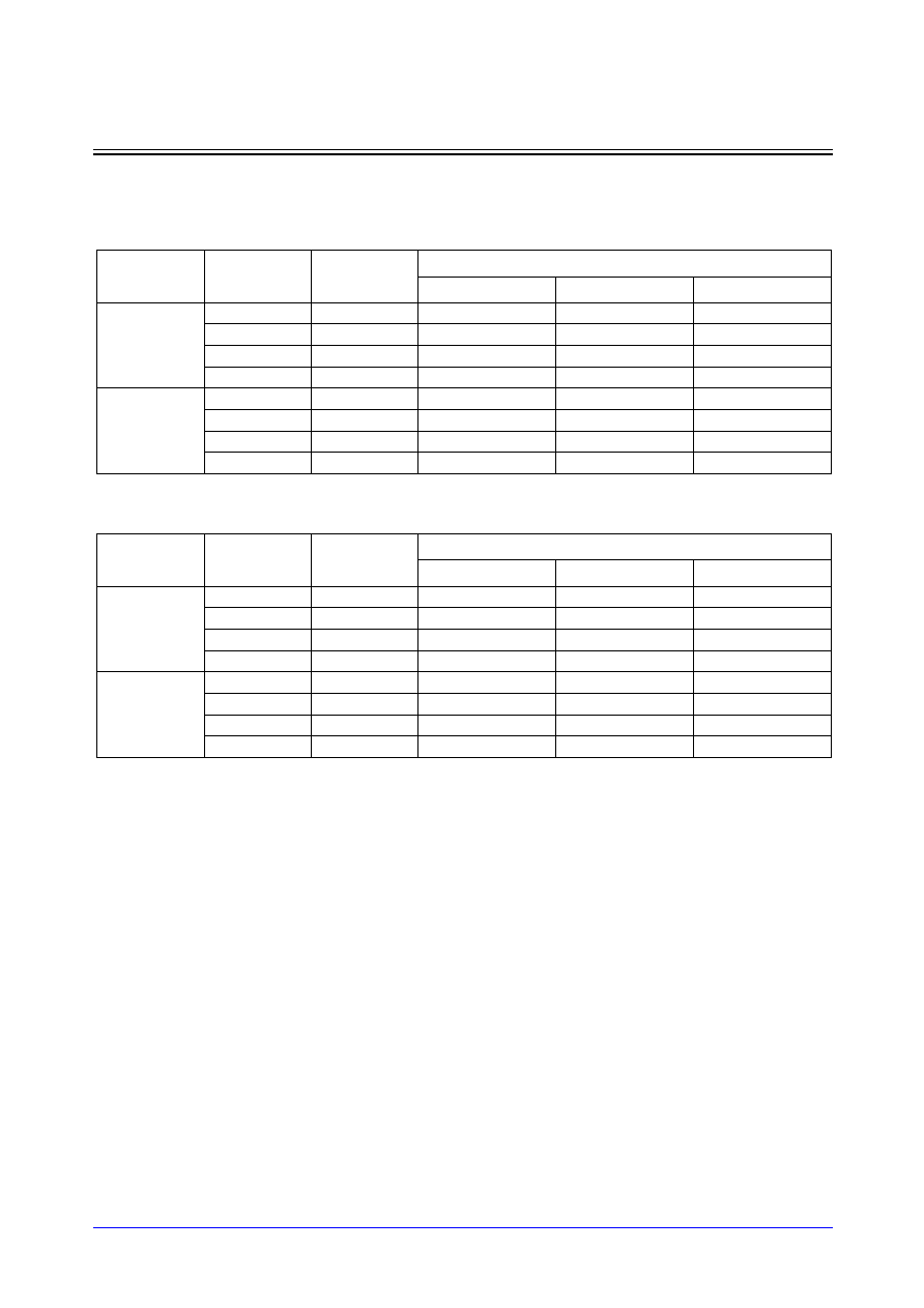
Samsung ASIC
4-127
STDL130
PHSOSCK17_LP/K27_LP/M16_LP/M26_LP/M36_LP
3.3V Interface Oscillator Cell with Enable and Feedback Resistor
Switching Characteristics
PHSOSCK27_LP
(Typical process, 25
∞
C,1.8V, 3.3V, t
R
/t
F
= 3.00ns, CL: Capacitive Load[pF])
(Typical process, 25
∞
C, 1.8V, 3.3V, t
R
/t
F
= 3.00ns, SL: Standard Load)
Path
Parameter
Delay [ns]
CL = 50.0pF
Delay Equations [ns]
Group1*
Group2*
Group3*
PADA to
PADY
tR
228.430
19.530 + 4.178*CL
19.550 + 4.178*CL
19.520 + 4.178*CL
tF
239.240
24.365 + 4.298*CL
24.320 + 4.298*CL
24.350 + 4.298*CL
tPLH
98.650
12.387 + 1.725*CL
12.390 + 1.725*CL
12.390 + 1.725*CL
tPHL
110.530
9.430 + 2.022*CL
9.410 + 2.022*CL
9.410 + 2.022*CL
E to PADY
tR
228.310
19.360 + 4.179*CL
19.290 + 4.180*CL
19.320 + 4.180*CL
tF
238.410
23.985 + 4.289*CL
23.950 + 4.289*CL
23.950 + 4.289*CL
tPLH
99.199
12.939 + 1.725*CL
12.917 + 1.726*CL
12.890 + 1.726*CL
tPHL
110.900
9.815 + 2.022*CL
9.800 + 2.022*CL
9.800 + 2.022*CL
*Group1 : CL < 50, *Group2 : 50 CL
<
<
=
= 75, *Group3 : 75 < CL
Path
Parameter
Delay [ns]
SL = 2
Delay Equations [ns]
Group1*
Group2*
Group3*
PADA to
YN
tR
0.148
0.144 + 0.002*SL
0.145 + 0.002*SL
0.145 + 0.002*SL
tF
0.106
0.103 + 0.002*SL
0.103 + 0.002*SL
0.106 + 0.001*SL
tPLH
6.450
6.447 + 0.002*SL
6.447 + 0.002*SL
6.451 + 0.001*SL
tPHL
6.061
6.058 + 0.002*SL
6.058 + 0.001*SL
6.061 + 0.001*SL
E to YN
tR
0.148
0.144 + 0.002*SL
0.146 + 0.002*SL
0.145 + 0.002*SL
tF
0.106
0.104 + 0.001*SL
0.102 + 0.002*SL
0.106 + 0.001*SL
tPLH
6.735
6.732 + 0.002*SL
6.733 + 0.002*SL
6.736 + 0.001*SL
tPHL
6.249
6.246 + 0.002*SL
6.247 + 0.001*SL
6.249 + 0.001*SL
*Group1 : SL < 5, *Group2 : 5 SL
<
<
=
= 16, *Group3 : 16 < SL

STDL130
4-128
Samsung ASIC
PHSOSCK17_LP/K27_LP/M16_LP/M26_LP/M36_LP
3.3V Interface Oscillator Cell with Enable and Feedback Resistor
Switching Characteristics
PHSOSCM16_LP
(Typical process, 25
∞
C, 1.8V, 3.3V, t
R
/t
F
= 3.00ns, CL: Capacitive Load[pF])
(Typical process, 25
∞
C, 1.8V, 3.3V, t
R
/t
F
= 3.00ns, SL: Standard Load)
Path
Parameter
Delay [ns]
CL = 50.0pF
Delay Equations [ns]
Group1*
Group2*
Group3*
PADA to
PADY
tR
21.410
1.292 + 0.402*CL
1.354 + 0.401*CL
1.234 + 0.403*CL
tF
23.850
1.280 + 0.451*CL
1.456 + 0.448*CL
1.426 + 0.448*CL
tPLH
10.931
1.460 + 0.189*CL
1.463 + 0.189*CL
1.445 + 0.190*CL
tPHL
13.430
1.501 + 0.239*CL
1.484 + 0.239*CL
1.478 + 0.239*CL
E to PADY
tR
21.415
1.365 + 0.401*CL
1.303 + 0.402*CL
1.330 + 0.402*CL
tF
23.777
1.307 + 0.449*CL
1.437 + 0.447*CL
1.416 + 0.447*CL
tPLH
11.167
1.696 + 0.189*CL
1.677 + 0.190*CL
1.677 + 0.190*CL
tPHL
13.752
1.805 + 0.239*CL
1.800 + 0.239*CL
1.800 + 0.239*CL
*Group1 : CL < 50, *Group2 : 50 CL
<
<
=
= 75, *Group3 : 75 < CL
Path
Parameter
Delay [ns]
SL = 2
Delay Equations [ns]
Group1*
Group2*
Group3*
PADA to
YN
tR
0.141
0.137 + 0.002*SL
0.138 + 0.002*SL
0.136 + 0.002*SL
tF
0.107
0.105 + 0.001*SL
0.103 + 0.002*SL
0.107 + 0.001*SL
tPLH
1.724
1.721 + 0.002*SL
1.721 + 0.001*SL
1.724 + 0.001*SL
tPHL
1.139
1.136 + 0.002*SL
1.136 + 0.001*SL
1.139 + 0.001*SL
E to YN
tR
0.141
0.137 + 0.002*SL
0.138 + 0.002*SL
0.137 + 0.002*SL
tF
0.108
0.104 + 0.002*SL
0.105 + 0.002*SL
0.106 + 0.002*SL
tPLH
2.284
2.281 + 0.002*SL
2.282 + 0.001*SL
2.284 + 0.001*SL
tPHL
1.691
1.688 + 0.002*SL
1.689 + 0.001*SL
1.691 + 0.001*SL
*Group1 : SL < 5, *Group2 : 5 SL
<
<
=
= 16, *Group3 : 16 < SL

Samsung ASIC
4-129
STDL130
PHSOSCK17_LP/K27_LP/M16_LP/M26_LP/M36_LP
3.3V Interface Oscillator Cell with Enable and Feedback Resistor
Switching Characteristics
PHSOSCM26_LP
(Typical process, 25
∞
C, 1.8V, 3.3V, t
R
/t
F
= 3.00ns, CL: Capacitive Load[pF])
(Typical process, 25
∞
C, 1.8V, 3.3V, t
R
/t
F
= 3.00ns, SL: Standard Load)
Path
Parameter
Delay [ns]
CL = 50.0pF
Delay Equations [ns]
Group1*
Group2*
Group3*
PADA to
PADY
tR
5.794
0.757 + 0.101*CL
1.247 + 0.091*CL
0.229 + 0.105*CL
tF
6.268
0.768 + 0.110*CL
0.621 + 0.113*CL
0.539 + 0.114*CL
tPLH
3.691
1.321 + 0.047*CL
1.313 + 0.048*CL
1.275 + 0.048*CL
tPHL
4.268
1.287 + 0.060*CL
1.255 + 0.060*CL
1.234 + 0.061*CL
E to PADY
tR
5.620
0.312 + 0.106*CL
0.581 + 0.101*CL
0.839 + 0.097*CL
tF
6.182
0.421 + 0.115*CL
0.385 + 0.116*CL
0.733 + 0.111*CL
tPLH
4.045
1.623 + 0.048*CL
1.626 + 0.048*CL
1.680 + 0.048*CL
tPHL
4.751
1.708 + 0.061*CL
1.707 + 0.061*CL
1.706 + 0.061*CL
*Group1 : CL < 50, *Group2 : 50 CL
<
<
=
= 75, *Group3 : 75 < CL
Path
Parameter
Delay [ns]
SL = 2
Delay Equations [ns]
Group1*
Group2*
Group3*
PADA to
YN
tR
0.142
0.140 + 0.001*SL
0.140 + 0.001*SL
0.141 + 0.001*SL
tF
0.099
0.098 + 0.001*SL
0.098 + 0.001*SL
0.098 + 0.001*SL
tPLH
1.763
1.761 + 0.001*SL
1.762 + 0.001*SL
1.763 + 0.001*SL
tPHL
1.323
1.321 + 0.001*SL
1.322 + 0.001*SL
1.322 + 0.001*SL
E to YN
tR
0.142
0.140 + 0.001*SL
0.140 + 0.001*SL
0.142 + 0.001*SL
tF
0.099
0.098 + 0.001*SL
0.098 + 0.001*SL
0.097 + 0.001*SL
tPLH
2.332
2.330 + 0.001*SL
2.330 + 0.001*SL
2.331 + 0.001*SL
tPHL
1.945
1.944 + 0.001*SL
1.944 + 0.001*SL
1.945 + 0.001*SL
*Group1 : SL < 5, *Group2 : 5 SL
<
<
=
= 16, *Group3 : 16 < SL

STDL130
4-130
Samsung ASIC
PHSOSCK17_LP/K27_LP/M16_LP/M26_LP/M36_LP
3.3V Interface Oscillator Cell with Enable and Feedback Resistor
Switching Characteristics
PHSOSCM36_LP
(Typical process, 25
∞
C, 1.8V, 3.3V, t
R
/t
F
= 3.00ns, CL: Capacitive Load[pF])
(Typical process, 25
∞
C, 1.8V, 3.3V, t
R
/t
F
= 3.00ns, SL: Standard Load)
Path
Parameter
Delay [ns]
CL = 50.0pF
Delay Equations [ns]
Group1*
Group2*
Group3*
PADA to
PADY
tR
2.813
1.050 + 0.035*CL
0.983 + 0.037*CL
0.904 + 0.038*CL
tF
2.977
0.990 + 0.040*CL
0.919 + 0.041*CL
0.747 + 0.043*CL
tPLH
2.726
1.666 + 0.021*CL
1.738 + 0.020*CL
1.782 + 0.019*CL
tPHL
2.967
1.721 + 0.025*CL
1.766 + 0.024*CL
1.778 + 0.024*CL
E to PADY
tR
2.627
0.675 + 0.039*CL
0.642 + 0.040*CL
0.536 + 0.041*CL
tF
2.819
0.735 + 0.042*CL
0.657 + 0.043*CL
0.520 + 0.045*CL
tPLH
3.179
2.112 + 0.021*CL
2.174 + 0.020*CL
2.220 + 0.019*CL
tPHL
3.825
2.546 + 0.026*CL
2.601 + 0.024*CL
2.618 + 0.024*CL
*Group1 : CL < 50, *Group2 : 50 CL
<
<
=
= 75, *Group3 : 75 < CL
Path
Parameter
Delay [ns]
SL = 2
Delay Equations [ns]
Group1*
Group2*
Group3*
PADA to
YN
tR
0.141
0.140 + 0.001*SL
0.140 + 0.001*SL
0.140 + 0.001*SL
tF
0.098
0.097 + 0.001*SL
0.097 + 0.001*SL
0.097 + 0.001*SL
tPLH
2.224
2.222 + 0.001*SL
2.223 + 0.001*SL
2.224 + 0.001*SL
tPHL
1.886
1.885 + 0.001*SL
1.885 + 0.001*SL
1.886 + 0.001*SL
E to YN
tR
0.141
0.140 + 0.001*SL
0.140 + 0.001*SL
0.141 + 0.001*SL
tF
0.098
0.097 + 0.001*SL
0.096 + 0.001*SL
0.098 + 0.001*SL
tPLH
2.728
2.726 + 0.001*SL
2.727 + 0.001*SL
2.728 + 0.001*SL
tPHL
2.747
2.746 + 0.001*SL
2.746 + 0.001*SL
2.747 + 0.001*SL
*Group1 : SL < 5, *Group2 : 5 SL
<
<
=
= 16, *Group3 : 16 < SL

Samsung ASIC
4-131
STDL130
PMSOSCK1_LP/K2_LP/M1_LP/M2_LP
2.5V Interface Oscillator Cell with Enable
Logic Symbol
Truth Table
Cell Data
E
PADA
PADY
YN
PI
PO
0
0
0
0
0
1
0
0
0
0
1
1
0
1
0
0
0
1
0
1
0
0
1
1
1
0
1
1
0
1
1
0
1
1
1
0
1
1
0
0
0
1
1
1
0
0
1
1
Input Load (SL)
I/O Sizes
PMSOSCK1_LP/K2_LP
PMSOSCM1_LP/M2_LP
PMSOSCK1_LP/K2_LP PMSOSCM1_LP/M2_LP
E
E
3.77
3.77
2 I/O Slots
2 I/O Slots
E
PADA
PADY
YN
PO
PI

STDL130
4-132
Samsung ASIC
PMSOSCK1_LP/K2_LP/M1_LP/M2_LP
2.5V Interface Oscillator Cell with Enable
Switching Characteristics
PMSOSCK1_LP
(Typical process, 25
∞
C, 1.8V, 2.5V, t
R
/t
F
= 3.00ns, CL: Capacitive Load[pF])
(Typical process, 25
∞
C, 1.8V, 2.5V, t
R
/t
F
= 3.00ns, SL: Standard Load)
Path
Parameter
Delay [ns]
CL = 50.0pF
Delay Equations [ns]
Group1*
Group2*
Group3*
PADA to
PADY
tR
1688.400
144.400 + 30.880*CL 144.800 + 30.872*CL 144.800 + 30.872*CL
tF
1064.800
103.375 + 19.228*CL 103.600 + 19.224*CL 103.300 + 19.228*CL
tPLH
859.380
100.455 + 15.179*CL 100.540 + 15.177*CL 100.300 + 15.180*CL
tPHL
534.510
39.535 + 9.899*CL
39.550 + 9.899*CL
39.460 + 9.900*CL
E to PADY
tR
1688.400
144.650 + 30.875*CL 144.800 + 30.872*CL 144.800 + 30.872*CL
tF
1064.800
103.375 + 19.228*CL 103.600 + 19.224*CL 103.300 + 19.228*CL
tPLH
859.400
100.475 + 15.178*CL 100.400 + 15.180*CL 100.700 + 15.176*CL
tPHL
534.000
39.025 + 9.899*CL
39.040 + 9.899*CL
38.920 + 9.901*CL
*Group1 : CL < 50, *Group2 : 50 CL
<
<
=
= 75, *Group3 : 75 < CL
Path
Parameter
Delay [ns]
SL = 2
Delay Equations [ns]
Group1*
Group2*
Group3*
PADA to
YN
tR
0.140
0.138 + 0.001*SL
0.138 + 0.001*SL
0.139 + 0.001*SL
tF
0.100
0.099 + 0.001*SL
0.099 + 0.001*SL
0.098 + 0.001*SL
tPLH
12.216
12.214 + 0.001*SL
12.215 + 0.001*SL
12.216 + 0.001*SL
tPHL
12.189
12.187 + 0.001*SL
12.187 + 0.001*SL
12.188 + 0.001*SL
E to YN
tR
0.139
0.137 + 0.001*SL
0.138 + 0.001*SL
0.138 + 0.001*SL
tF
0.100
0.098 + 0.001*SL
0.098 + 0.001*SL
0.100 + 0.001*SL
tPLH
12.099
12.097 + 0.001*SL
12.097 + 0.001*SL
12.097 + 0.001*SL
tPHL
11.779
11.777 + 0.001*SL
11.777 + 0.001*SL
11.778 + 0.001*SL
*Group1 : SL < 5, *Group2 : 5 SL
<
<
=
= 16, *Group3 : 16 < SL

Samsung ASIC
4-133
STDL130
PMSOSCK1_LP/K2_LP/M1_LP/M2_LP
2.5V Interface Oscillator Cell with Enable
Switching Characteristics
PMSOSCK2_LP
(Typical process, 25
∞
C, 1.8V, 2.5V, t
R
/t
F
= 3.00ns, CL: Capacitive Load[pF])
(Typical process, 25
∞
C, 1.8V, 2.5V, t
R
/t
F
= 3.00ns, SL: Standard Load)
Path
Parameter
Delay [ns]
CL = 50.0pF
Delay Equations [ns]
Group1*
Group2*
Group3*
PADA to
PADY
tR
211.590
17.215 + 3.888*CL
17.250 + 3.887*CL
17.220 + 3.887*CL
tF
209.890
20.715 + 3.783*CL
20.670 + 3.784*CL
20.700 + 3.784*CL
tPLH
92.941
11.556 + 1.628*CL
11.543 + 1.628*CL
11.570 + 1.628*CL
tPHL
96.079
7.637 + 1.769*CL
7.617 + 1.769*CL
7.650 + 1.769*CL
E to PADY
tR
211.590
17.215 + 3.888*CL
17.250 + 3.887*CL
17.220 + 3.887*CL
tF
209.890
20.715 + 3.783*CL
20.690 + 3.784*CL
20.660 + 3.784*CL
tPLH
92.837
11.454 + 1.628*CL
11.451 + 1.628*CL
11.430 + 1.628*CL
tPHL
95.658
7.215 + 1.769*CL
7.214 + 1.769*CL
7.190 + 1.769*CL
*Group1 : CL < 50, *Group2 : 50 CL
<
<
=
= 75, *Group3 : 75 < CL
Path
Parameter
Delay [ns]
SL = 2
Delay Equations [ns]
Group1*
Group2*
Group3*
PADA to
YN
tR
0.139
0.137 + 0.001*SL
0.138 + 0.001*SL
0.138 + 0.001*SL
tF
0.100
0.098 + 0.001*SL
0.098 + 0.001*SL
0.100 + 0.001*SL
tPLH
7.436
7.434 + 0.001*SL
7.435 + 0.001*SL
7.436 + 0.001*SL
tPHL
6.542
6.541 + 0.001*SL
6.541 + 0.001*SL
6.542 + 0.001*SL
E to YN
tR
0.140
0.138 + 0.001*SL
0.137 + 0.001*SL
0.140 + 0.001*SL
tF
0.100
0.099 + 0.001*SL
0.099 + 0.001*SL
0.098 + 0.001*SL
tPLH
7.382
7.380 + 0.001*SL
7.381 + 0.001*SL
7.382 + 0.001*SL
tPHL
5.982
5.981 + 0.001*SL
5.981 + 0.001*SL
5.982 + 0.001*SL
*Group1 : SL < 5, *Group2 : 5 SL
<
<
=
= 16, *Group3 : 16 < SL

STDL130
4-134
Samsung ASIC
PMSOSCK1_LP/K2_LP/M1_LP/M2_LP
2.5V Interface Oscillator Cell with Enable
Switching Characteristics
PMSOSCM1_LP
(Typical process, 25
∞
C, 1.8V, 2.5V, t
R
/t
F
= 3.00ns, CL: Capacitive Load[pF])
(Typical process, 25
∞
C, 1.8V, 2.5V, t
R
/t
F
= 3.00ns, SL: Standard Load)
Path
Parameter
Delay [ns]
CL = 50.0pF
Delay Equations [ns]
Group1*
Group2*
Group3*
PADA to
PADY
tR
13.538
0.899 + 0.253*CL
0.460 + 0.262*CL
0.541 + 0.260*CL
tF
14.851
0.533 + 0.286*CL
0.697 + 0.283*CL
0.598 + 0.284*CL
tPLH
7.666
1.421 + 0.125*CL
1.381 + 0.126*CL
1.406 + 0.125*CL
tPHL
9.070
1.430 + 0.153*CL
1.427 + 0.153*CL
1.425 + 0.153*CL
E to PADY
tR
13.611
0.682 + 0.259*CL
0.659 + 0.259*CL
0.566 + 0.260*CL
tF
14.845
0.446 + 0.288*CL
0.731 + 0.282*CL
0.548 + 0.285*CL
tPLH
7.698
1.391 + 0.126*CL
1.423 + 0.126*CL
1.431 + 0.125*CL
tPHL
8.960
1.304 + 0.153*CL
1.312 + 0.153*CL
1.309 + 0.153*CL
*Group1 : CL < 50, *Group2 : 50 CL
<
<
=
= 75, *Group3 : 75 < CL
Path
Parameter
Delay [ns]
SL = 2
Delay Equations [ns]
Group1*
Group2*
Group3*
PADA to
YN
tR
0.146
0.145 + 0.001*SL
0.145 + 0.001*SL
0.146 + 0.001*SL
tF
0.099
0.097 + 0.001*SL
0.098 + 0.001*SL
0.097 + 0.001*SL
tPLH
2.193
2.191 + 0.001*SL
2.192 + 0.001*SL
2.193 + 0.001*SL
tPHL
1.657
1.655 + 0.001*SL
1.656 + 0.001*SL
1.657 + 0.001*SL
E to YN
tR
0.146
0.144 + 0.001*SL
0.144 + 0.001*SL
0.146 + 0.001*SL
tF
0.099
0.097 + 0.001*SL
0.098 + 0.001*SL
0.097 + 0.001*SL
tPLH
2.349
2.348 + 0.001*SL
2.348 + 0.001*SL
2.349 + 0.001*SL
tPHL
1.642
1.641 + 0.001*SL
1.641 + 0.001*SL
1.642 + 0.001*SL
*Group1 : SL < 5, *Group2 : 5 SL
<
<
=
= 16, *Group3 : 16 < SL

Samsung ASIC
4-135
STDL130
PMSOSCK1_LP/K2_LP/M1_LP/M2_LP
2.5V Interface Oscillator Cell with Enable
Switching Characteristics
PMSOSCM2_LP
(Typical process, 25
∞
C, 1.8V, 2.5V, t
R
/t
F
= 3.00ns, CL: Capacitive Load[pF])
(Typical process, 25
∞
C, 1.8V, 2.5V, t
R
/t
F
= 3.00ns, SL: Standard Load)
Path
Parameter
Delay [ns]
CL = 50.0pF
Delay Equations [ns]
Group1*
Group2*
Group3*
PADA to
PADY
tR
4.188
0.517 + 0.073*CL
1.241 + 0.059*CL
1.031 + 0.062*CL
tF
4.102
0.782 + 0.066*CL
0.828 + 0.065*CL
0.640 + 0.068*CL
tPLH
3.689
2.030 + 0.033*CL
2.088 + 0.032*CL
2.140 + 0.031*CL
tPHL
4.014
2.118 + 0.038*CL
2.150 + 0.037*CL
2.162 + 0.037*CL
E to PADY
tR
4.106
0.584 + 0.070*CL
1.404 + 0.054*CL
0.403 + 0.067*CL
tF
3.996
0.759 + 0.065*CL
0.584 + 0.068*CL
0.341 + 0.071*CL
tPLH
3.829
2.153 + 0.034*CL
2.223 + 0.032*CL
2.257 + 0.032*CL
tPHL
4.332
2.431 + 0.038*CL
2.462 + 0.037*CL
2.476 + 0.037*CL
*Group1 : CL < 50, *Group2 : 50 CL
<
<
=
= 75, *Group3 : 75 < CL
Path
Parameter
Delay [ns]
SL = 2
Delay Equations [ns]
Group1*
Group2*
Group3*
PADA to
YN
tR
0.146
0.145 + 0.001*SL
0.144 + 0.001*SL
0.146 + 0.001*SL
tF
0.099
0.097 + 0.001*SL
0.098 + 0.001*SL
0.096 + 0.001*SL
tPLH
2.676
2.674 + 0.001*SL
2.674 + 0.001*SL
2.675 + 0.001*SL
tPHL
2.236
2.235 + 0.001*SL
2.235 + 0.001*SL
2.236 + 0.001*SL
E to YN
tR
0.146
0.144 + 0.001*SL
0.145 + 0.001*SL
0.145 + 0.001*SL
tF
0.098
0.097 + 0.001*SL
0.097 + 0.001*SL
0.098 + 0.001*SL
tPLH
2.809
2.808 + 0.001*SL
2.808 + 0.001*SL
2.809 + 0.001*SL
tPHL
2.541
2.540 + 0.001*SL
2.540 + 0.001*SL
2.540 + 0.001*SL
*Group1 : SL < 5, *Group2 : 5 SL
<
<
=
= 16, *Group3 : 16 < SL
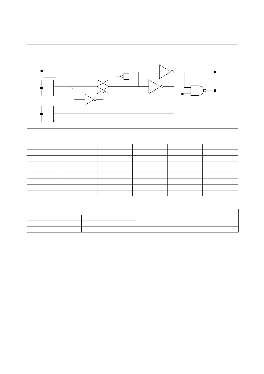
STDL130
4-136
Samsung ASIC
PSOSCK1_LP/K2_LP/M1_LP/M2_LP
1.8V Interface Oscillator Cell with Enable
Logic Symbol
Truth Table
Cell Data
E
PADA
PADY
YN
PI
PO
0
0
0
0
0
1
0
0
0
0
1
1
0
1
0
0
0
1
0
1
0
0
1
1
1
0
1
1
0
1
1
0
1
1
1
0
1
1
0
0
0
1
1
1
0
0
1
1
Input Load (SL)
I/O Sizes
PSOSCK1_LP/K2_LP
PSOSCM1_LP/M2_LP
PSOSCK1_LP/K2_LP
PSOSCM1_LP/M2_LP
E
E
3.75
3.75
2 I/O Slots
2 I/O Slots
E
PADA
PADY
YN
PO
PI

Samsung ASIC
4-137
STDL130
PSOSCK1_LP/K2_LP/M1_LP/M2_LP
1.8V Interface Oscillator Cell with Enable
Switching Characteristics
PSOSCK1_LP
(Typical process, 25
∞
C, 1.8V, t
R
/t
F
= 3.00ns, CL: Capacitive Load[pF])
(Typical process, 25
∞
C, 1.8V, t
R
/t
F
= 3.00ns, SL: Standard Load)
Path
Parameter
Delay [ns]
CL = 50.0pF
Delay Equations [ns]
Group1*
Group2*
Group3*
PADA to
PADY
tR
1163.100
146.575 + 20.330*CL 147.500 + 20.312*CL 147.200 + 20.316*CL
tF
1473.200
214.150 + 25.181*CL 212.600 + 25.212*CL 212.000 + 25.220*CL
tPLH
617.920
111.595 + 10.126*CL 111.980 + 10.119*CL 112.160 + 10.116*CL
tPHL
707.440
78.740 + 12.574*CL
78.720 + 12.574*CL
78.900 + 12.572*CL
E to PADY
tR
1163.100
146.575 + 20.330*CL 147.500 + 20.312*CL 147.200 + 20.316*CL
tF
1473.100
212.975 + 25.202*CL 212.300 + 25.216*CL 212.000 + 25.220*CL
tPLH
617.830
111.505 + 10.127*CL 111.890 + 10.119*CL 112.100 + 10.116*CL
tPHL
703.930
75.255 + 12.573*CL
75.190 + 12.575*CL
75.400 + 12.572*CL
*Group1 : CL < 50, *Group2 : 50 CL
<
<
=
= 75, *Group3 : 75 < CL
Path
Parameter
Delay [ns]
SL = 2
Delay Equations [ns]
Group1*
Group2*
Group3*
PADA to
YN
tR
0.107
0.101 + 0.003*SL
0.103 + 0.003*SL
0.102 + 0.003*SL
tF
0.101
0.091 + 0.005*SL
0.095 + 0.004*SL
0.083 + 0.005*SL
tPLH
119.063
119.057 + 0.003*SL
119.062 + 0.002*SL
119.056 + 0.002*SL
tPHL
127.263
127.257 + 0.003*SL
127.255 + 0.003*SL
127.262 + 0.003*SL
E to YN
tR
0.107
0.101 + 0.003*SL
0.102 + 0.003*SL
0.101 + 0.003*SL
tF
0.101
0.091 + 0.005*SL
0.093 + 0.004*SL
0.088 + 0.005*SL
tPLH
118.970
118.970 + 0.000*SL
118.959 + 0.003*SL
118.966 + 0.002*SL
tPHL
120.223
120.217 + 0.003*SL
120.215 + 0.003*SL
120.229 + 0.002*SL
*Group1 : SL < 5, *Group2 : 5 SL
<
<
=
= 16, *Group3 : 16 < SL

STDL130
4-138
Samsung ASIC
PSOSCK1_LP/K2_LP/M1_LP/M2_LP
1.8V Interface Oscillator Cell with Enable
Switching Characteristics
PSOSCK2_LP
(Typical process, 25
∞
C, 1.8V, t
R
/t
F
= 3.00ns, CL: Capacitive Load[pF])
(Typical process, 25
∞
C, 1.8V, t
R
/t
F
= 3.00ns, SL: Standard Load)
Path
Parameter
Delay [ns]
CL = 50.0pF
Delay Equations [ns]
Group1*
Group2*
Group3*
PADA to
PADY
tR
149.960
17.500 + 2.649*CL
17.620 + 2.647*CL
17.740 + 2.645*CL
tF
203.440
29.890 + 3.471*CL
29.840 + 3.472*CL
29.900 + 3.471*CL
tPLH
63.334
12.544 + 1.016*CL
12.872 + 1.009*CL
13.100 + 1.006*CL
tPHL
91.876
11.876 + 1.600*CL
11.888 + 1.600*CL
11.900 + 1.600*CL
E to PADY
tR
149.960
17.500 + 2.649*CL
17.620 + 2.647*CL
17.710 + 2.646*CL
tF
203.270
29.570 + 3.474*CL
29.590 + 3.474*CL
29.530 + 3.474*CL
tPLH
62.976
12.186 + 1.016*CL
12.510 + 1.009*CL
12.756 + 1.006*CL
tPHL
90.441
10.466 + 1.600*CL
10.443 + 1.600*CL
10.470 + 1.600*CL
*Group1 : CL < 50, *Group2 : 50 CL
<
<
=
= 75, *Group3 : 75 < CL
Path
Parameter
Delay [ns]
SL = 2
Delay Equations [ns]
Group1*
Group2*
Group3*
PADA to
YN
tR
0.099
0.093 + 0.003*SL
0.094 + 0.003*SL
0.094 + 0.003*SL
tF
0.087
0.078 + 0.005*SL
0.079 + 0.004*SL
0.077 + 0.005*SL
tPLH
29.663
29.657 + 0.003*SL
29.660 + 0.002*SL
29.668 + 0.002*SL
tPHL
31.635
31.628 + 0.003*SL
31.631 + 0.003*SL
31.634 + 0.003*SL
E to YN
tR
0.098
0.092 + 0.003*SL
0.093 + 0.003*SL
0.094 + 0.003*SL
tF
0.088
0.079 + 0.004*SL
0.079 + 0.004*SL
0.076 + 0.005*SL
tPLH
29.586
29.581 + 0.003*SL
29.583 + 0.002*SL
29.591 + 0.002*SL
tPHL
28.671
28.665 + 0.003*SL
28.666 + 0.003*SL
28.669 + 0.003*SL
*Group1 : SL < 5, *Group2 : 5 SL
<
<
=
= 16, *Group3 : 16 < SL

Samsung ASIC
4-139
STDL130
PSOSCK1_LP/K2_LP/M1_LP/M2_LP
1.8V Interface Oscillator Cell with Enable
Switching Characteristics
PSOSCM1_LP
(Typical process, 25
∞
C, 1.8V, t
R
/t
F
= 3.00ns, CL: Capacitive Load[pF])
(Typical process, 25
∞
C, 1.8V, t
R
/t
F
= 3.00ns, SL: Standard Load)
Path
Parameter
Delay [ns]
CL = 50.0pF
Delay Equations [ns]
Group1*
Group2*
Group3*
PADA to
PADY
tR
13.238
1.316 + 0.238*CL
1.212 + 0.241*CL
1.020 + 0.243*CL
tF
19.329
1.699 + 0.353*CL
1.579 + 0.355*CL
1.570 + 0.355*CL
tPLH
7.565
1.789 + 0.116*CL
1.806 + 0.115*CL
1.817 + 0.115*CL
tPHL
11.527
1.961 + 0.191*CL
1.961 + 0.191*CL
1.961 + 0.191*CL
E to PADY
tR
13.246
1.269 + 0.240*CL
1.264 + 0.240*CL
0.970 + 0.244*CL
tF
19.314
1.714 + 0.352*CL
1.554 + 0.355*CL
1.542 + 0.355*CL
tPLH
7.337
1.559 + 0.116*CL
1.583 + 0.115*CL
1.574 + 0.115*CL
tPHL
11.265
1.694 + 0.191*CL
1.699 + 0.191*CL
1.702 + 0.191*CL
*Group1 : CL < 50, *Group2 : 50 CL
<
<
=
= 75, *Group3 : 75 < CL
Path
Parameter
Delay [ns]
SL = 2
Delay Equations [ns]
Group1*
Group2*
Group3*
PADA to
YN
tR
0.098
0.093 + 0.003*SL
0.092 + 0.003*SL
0.092 + 0.003*SL
tF
0.091
0.082 + 0.005*SL
0.083 + 0.004*SL
0.081 + 0.004*SL
tPLH
1.371
1.365 + 0.003*SL
1.367 + 0.002*SL
1.376 + 0.002*SL
tPHL
1.384
1.377 + 0.003*SL
1.379 + 0.003*SL
1.383 + 0.003*SL
E to YN
tR
0.094
0.089 + 0.003*SL
0.088 + 0.003*SL
0.087 + 0.003*SL
tF
0.086
0.077 + 0.005*SL
0.078 + 0.004*SL
0.076 + 0.005*SL
tPLH
1.355
1.349 + 0.003*SL
1.352 + 0.002*SL
1.359 + 0.002*SL
tPHL
1.229
1.222 + 0.003*SL
1.224 + 0.003*SL
1.228 + 0.003*SL
*Group1 : SL < 5, *Group2 : 5 SL
<
<
=
= 16, *Group3 : 16 < SL

STDL130
4-140
Samsung ASIC
PSOSCK1_LP/K2_LP/M1_LP/M2_LP
1.8V Interface Oscillator Cell with Enable
Switching Characteristics
PSOSCM2_LP
(Typical process, 25
∞
C, 1.8V, t
R
/t
F
= 3.00ns, CL: Capacitive Load[pF])
(Typical process, 25
∞
C, 1.8V, t
R
/t
F
= 3.00ns, SL: Standard Load)
Path
Parameter
Delay [ns]
CL = 50.0pF
Delay Equations [ns]
Group1*
Group2*
Group3*
PADA to
PADY
tR
3.718
1.320 + 0.048*CL
0.417 + 0.066*CL
1.741 + 0.048*CL
tF
5.129
0.611 + 0.090*CL
0.900 + 0.085*CL
0.296 + 0.093*CL
tPLH
3.599
2.058 + 0.031*CL
2.117 + 0.030*CL
2.144 + 0.029*CL
tPHL
4.409
2.010 + 0.048*CL
2.015 + 0.048*CL
2.023 + 0.048*CL
E to PADY
tR
3.666
1.129 + 0.051*CL
0.335 + 0.067*CL
1.654 + 0.049*CL
tF
5.107
0.370 + 0.095*CL
0.698 + 0.088*CL
1.016 + 0.084*CL
tPLH
3.140
1.600 + 0.031*CL
1.657 + 0.030*CL
1.689 + 0.029*CL
tPHL
3.999
1.600 + 0.048*CL
1.609 + 0.048*CL
1.600 + 0.048*CL
*Group1 : CL < 50, *Group2 : 50 CL
<
<
=
= 75, *Group3 : 75 < CL
Path
Parameter
Delay [ns]
SL = 2
Delay Equations [ns]
Group1*
Group2*
Group3*
PADA to
YN
tR
0.079
0.074 + 0.003*SL
0.074 + 0.003*SL
0.072 + 0.003*SL
tF
0.084
0.075 + 0.004*SL
0.074 + 0.005*SL
0.074 + 0.005*SL
tPLH
1.609
1.604 + 0.002*SL
1.606 + 0.002*SL
1.611 + 0.002*SL
tPHL
1.675
1.669 + 0.003*SL
1.670 + 0.003*SL
1.673 + 0.003*SL
E to YN
tR
0.073
0.068 + 0.003*SL
0.068 + 0.003*SL
0.067 + 0.003*SL
tF
0.079
0.071 + 0.004*SL
0.070 + 0.005*SL
0.070 + 0.005*SL
tPLH
1.235
1.231 + 0.002*SL
1.232 + 0.002*SL
1.237 + 0.002*SL
tPHL
1.366
1.360 + 0.003*SL
1.361 + 0.003*SL
1.364 + 0.003*SL
*Group1 : SL < 5, *Group2 : 5 SL
<
<
=
= 16, *Group3 : 16 < SL
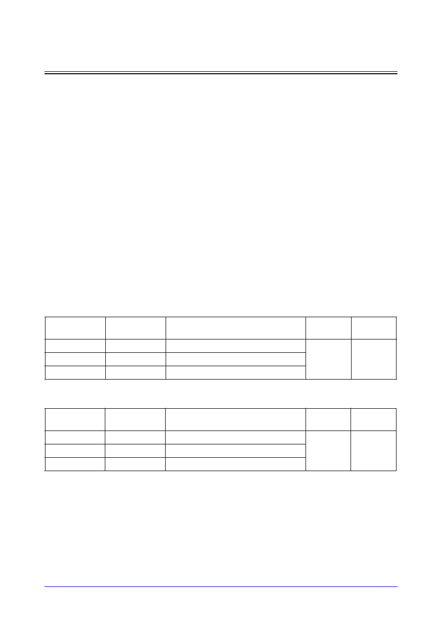
Samsung ASIC
4-141
STDL130
PCI BUFFERS
Overview
PCI buffers are designed for PCI local bus application which is intended for high-performance 32-bit or 64-bit
bus architecture.
Samsung supports PCI input, output and bi-directional buffers for 3.3V and 5V signaling environment.
Features
--
Low-power, high performance CMOS technology
--
Input, output, and bi-directional PCI buffers
--
Operating at up to 66MHz, including 33MHz
--
Electrically compliant interface in 3.3V and 5V bus environments
Description
These PCI buffers are designed for 3.3V and 5V environments. These buffers are compliant with PCI local
bus specification rev2.1. The PCI buffers for 66MHz can be available in 33MHz interface, but require more
power pads due to their fast and noisy characteristics. The 5V tolerant PCI buffers can be used for 33MHz,
5V environment. These tolerant PCI buffers require 5V power for bulk of PMOS driver for 5V environment or
3.3V power for 3.3V environment. The 5V tolerant PCI drivers support 5V environment while EN5V is low.
Although tolerant PCI buffers support 5V environment, they do not drive 5V.
NOTE:
If you want to use PCI buffers, please contact Samsung.
Cell List
3.3V Signaling PCI I/Os
5V Signaling PCI I/Os
NOTE1: 3.3V signaling conditions: EN5V=high, VIO=3.3V, In this case 5V tolerant is not supported.
5V signaling conditions: EN5V=low, VIO=5V, and 5V tolerant is supported.
NOTE2: In 3.3V signaling, the voltage of VIO is 3.3V, which is provided through the VDD5O_PCI_LP power cell.
In 5V signaling, the voltage of VIO is 5V, which is provided through the VDD5O_PCI_LP power cell.
Cell Name
Description
Operating Frequency
VIO
(note2)
Voltage
Operating
Voltage
PTBPCI3_LP
Bi-direction
Up to 66MHz at 3.3V signaling
(note1)
3.3V
3.3V
PTOPCI3_LP
Driver
Up to 66MHz at 3.3V signaling
PTIPCI3_LP
Receiver
Up to 66MHz at 3.3V signaling
Cell Name
Description
Operating Frequency
VIO
(note2)
Voltage
Operating
Voltage
PTBPCI5_LP
Bi-direction
Up to 33MHz at 5V signaling
(note1)
5V
3.3V
PTOPCI5_LP
Driver
Up to 33MHz at 5V signaling
PTIPCI5_LP
Receiver
Up to 33MHz at 5V signaling
STDL130
4-142
Samsung ASIC
PCI BUFFERS
Option
(note3)
NOTE3: Voltage detector circuit will automatically set the EN5V pin either high or low according to VIO voltage level.
Electrical Characteristics
DC Characteristics
AC Characteristics
Power Cell Name
Description
VDD1IH_PCI_LP
1.8V power cell for internal core and PCI I/Os
VDD3OP_PCI_LP
3.3V power cell for PCI I/Os
VDD5O_PCI_LP
VIO(3.3V or 5V) power cell for PCI I/Os
(note2)
VSS3I_PCI_LP
Gnd power cell for internal core; not used for PCI I/Os
VSS3OP_PCI_LP
Gnd power cell for PCI I/Os
Cell Name
Description
VDET_L130PCI_LP
3.3V or 5V voltage detector
Symbol
Parameter
3.3V Signaling
5V Signaling
Unit
Condition
Min
Max
Condition
Min
Max
V
cc
Supply Voltage
3.0
3.6
3.0
3.6
V
V
IO
V
IO
Voltage
V
CC
4.75
5.25
V
V
ih
Input high voltage
0.47V
CC
V
CC
+0.5
1.9
V
IO
+0.5
V
V
il
Input low voltage
≠0.5
0.33V
CC
≠0.5
0.9
V
I
i
Input leakage
current
0 < V
IN
< V
CC
≠10
10
0 < V
IN
< VIO
≠70
70
µ
A
V
oh
Output high voltage
I
OUT
= ≠500
µ
A
0.9V
CC
≠
I
OUT
= ≠2mA
2.4
≠
V
V
ol
Output low voltage
I
OUT
= 1500
µ
A
≠
0.1V
CC
I
OUT
= 6mA
≠
0.55
V
Symbol
Parameter
3.3V Signaling (66MHz)
5V Signaling (33MHz)
Unit
Condition
Min
Max
Condition
Min
Max
I
oh (AC)
Switching
current high
V
OUT
= 0.3V
CC
≠12V
CC
V
OUT
= 1.4V
≠44
mA
V
OUT
= 0.7V
CC
≠32V
CC
V
OUT
= 2.4V
≠2.33
V
OUT
= 0.9V
CC
≠1.71V
CC
V
OUT
= 3.0V
≠142
I
ol (AC)
Switching
current low
V
OUT
= 0.6V
CC
16V
CC
V
OUT
= 2.2V
95
mA
V
OUT
= 0.1V
CC
2.67V
CC
V
OUT
= 0.55V
23.9
V
OUT
= 0.18V
CC
38V
CC
V
OUT
= 0.71V
206
I
cl
Low clamp
current
≠3
<
V
IN
≠1
≠25 +
(V
IN
+1)/0.015
≠5
<
V
IN
≠1
≠25 + (V
IN
+1)
/0.015
mA
I
ch
High clamp
current
V
CC
+1
V
IN
< V
CC
+4
25+(V
IN
≠V
CC
≠1)
/0.015
mA
T
r
Output rise
time
0.3V
CC
to 0.6V
CC
1.0
4.0
0.4V to 2.4V
1.0
5.0
V/ns
T
f
Output fall
time
0.6V
CC
to 0.3V
CC
1.0
4.0
2.4V to 0.4V
1.0
5.0
V/ns
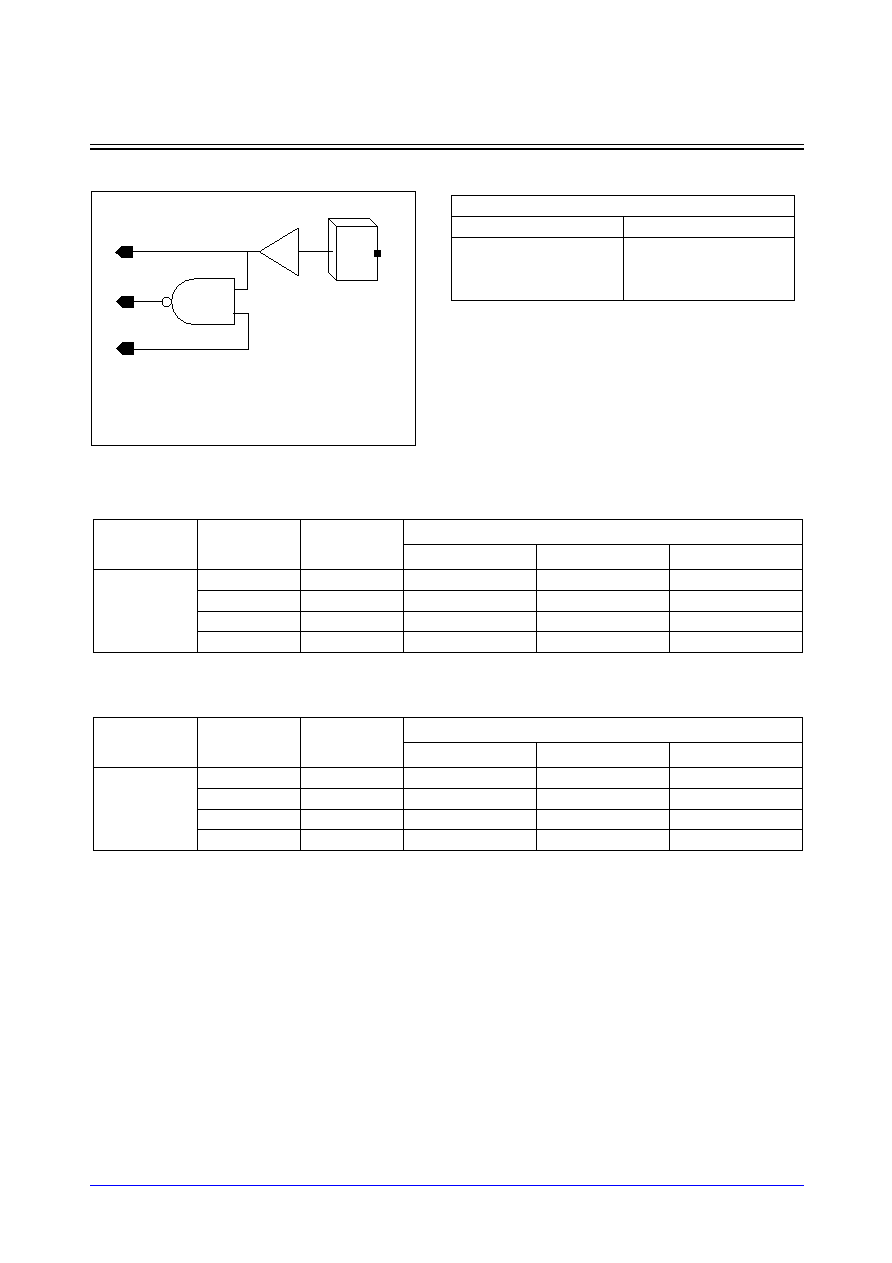
Samsung ASIC
4-143
STDL130
PTIPCI_LP
5V-tolerant PCI Input Buffers
Logic Symbol
Switching Characteristics
(Typical process, 25
∞
C, 1.8V, 3.3V, t
R
/t
F
= 3.00ns, SL: Standard Load)
PTIPCI3_LP
PTIPCI5_LP
Truth Table
Input Truth Table
PAD
PI
Y
PO
1
1
1
0
0
x
0
1
1
0
1
1
PAD
Y
PO
PI
Path
Parameter
Delay [ns]
SL = 2
Delay Equations [ns]
Group1*
Group2*
Group3*
PAD to Y
tR
0.263
0.243 + 0.010*SL
0.243 + 0.010*SL
0.242 + 0.010*SL
tF
0.107
0.099 + 0.004*SL
0.099 + 0.004*SL
0.110 + 0.003*SL
tPLH
0.685
0.676 + 0.005*SL
0.676 + 0.004*SL
0.683 + 0.004*SL
tPHL
0.539
0.529 + 0.006*SL
0.531 + 0.004*SL
0.551 + 0.003*SL
*Group1 : SL < 1, *Group2 : 1 SL
<
<
=
= 15, *Group3 : 15 < SL
Path
Parameter
Delay [ns]
SL = 2
Delay Equations [ns]
Group1*
Group2*
Group3*
PAD to Y
tR
0.254
0.235 + 0.009*SL
0.235 + 0.009*SL
0.236 + 0.009*SL
tF
0.092
0.084 + 0.004*SL
0.085 + 0.004*SL
0.091 + 0.003*SL
tPLH
0.548
0.541 + 0.004*SL
0.541 + 0.004*SL
0.548 + 0.003*SL
tPHL
0.554
0.546 + 0.005*SL
0.547 + 0.003*SL
0.564 + 0.002*SL
*Group1 : SL < 1, *Group2 : 1 SL
<
<
=
= 15, *Group3 : 15 < SL
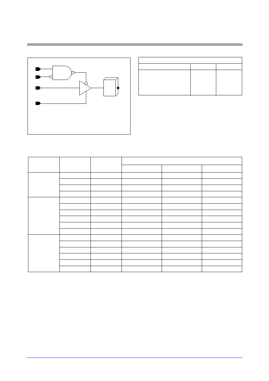
STDL130
4-144
Samsung ASIC
PTOPCI_LP
5V-tolerant PCI Output Buffers
Logic Symbol
Switching Characteristics
(Typical process, 25
∞
C, 1.8V, 3.3V, t
R
/t
F
=0.17ns, CL: Capacitive Load[pF])
PTOPCI3_LP
PAD
A
TN
EN
EN5V
NOTE:
EN5V=Low: Enable the 5V signaling
EN5V=High: Enable the 3.3V signaling
Path
Parameter
Delay [ns]
CL = 50.0pF
Delay Equations [ns]
Group1*
Group2*
Group3*
A to PAD
tR
1.436
0.433 + 0.023*CL
0.624 + 0.016*CL
0.714 + 0.014*CL
tF
1.519
0.447 + 0.020*CL
0.351 + 0.023*CL
0.284 + 0.025*CL
tPLH
2.032
1.038 + 0.022*CL
1.233 + 0.016*CL
1.384 + 0.013*CL
tPHL
2.844
1.307 + 0.032*CL
1.420 + 0.028*CL
1.494 + 0.027*CL
TN to PAD
tR
1.436
0.435 + 0.023*CL
0.626 + 0.016*CL
0.715 + 0.014*CL
tF
1.501
0.375 + 0.022*CL
0.301 + 0.024*CL
0.253 + 0.025*CL
tPLH
2.208
1.212 + 0.023*CL
1.408 + 0.016*CL
1.560 + 0.013*CL
tPHL
2.959
1.381 + 0.033*CL
1.523 + 0.029*CL
1.603 + 0.027*CL
tPLZ
0.779
0.779 + 0.000*CL
0.779 + 0.000*CL
0.779 + 0.000*CL
tPHZ
0.947
0.946 + 0.000*CL
0.946 + 0.000*CL
0.947 + 0.000*CL
EN to PAD
tR
1.436
0.435 + 0.023*CL
0.626 + 0.016*CL
0.715 + 0.014*CL
tF
1.501
0.375 + 0.022*CL
0.301 + 0.024*CL
0.253 + 0.025*CL
tPLH
2.279
1.283 + 0.023*CL
1.480 + 0.016*CL
1.631 + 0.013*CL
tPHL
3.030
1.453 + 0.033*CL
1.595 + 0.029*CL
1.674 + 0.027*CL
tPLZ
0.783
0.783 + 0.000*CL
0.783 + 0.000*CL
0.783 + 0.000*CL
tPHZ
0.951
0.949 + 0.000*CL
0.949 + 0.000*CL
0.950 + 0.000*CL
*Group1 : CL < 30, *Group2 : 30 CL
<
<
=
= 50, *Group3 : 50 < CL
Truth Table
Output Truth Table
A
EN
TN
PAD
0
0
1
0
1
0
1
1
x
1
x
Hi-Z
x
x
0
HI-Z
Samsung ASIC
4-145
STDL130
PTOPCI_LP
5V-tolerant PCI Output Buffers
Switching Characteristics
(Typical process, 25
∞
C, 1.8V, 3.3V, t
R
/t
F
=0.17ns, CL: Capacitive Load[pF])
PTOPCI5_LP
Path
Parameter
Delay [ns]
CL = 50.0pF
Delay Equations [ns]
Group1*
Group2*
Group3*
A to PAD
tR
1.243
0.460 + 0.017*CL
0.584 + 0.013*CL
0.632 + 0.012*CL
tF
0.978
0.380 + 0.011*CL
0.331 + 0.013*CL
0.281 + 0.014*CL
tPLH
2.064
1.249 + 0.018*CL
1.400 + 0.013*CL
1.513 + 0.011*CL
tPHL
2.378
1.267 + 0.024*CL
1.417 + 0.019*CL
1.523 + 0.017*CL
TN to PAD
tR
1.252
0.515 + 0.016*CL
0.619 + 0.013*CL
0.650 + 0.012*CL
tF
0.965
0.340 + 0.012*CL
0.294 + 0.013*CL
0.261 + 0.014*CL
tPLH
2.234
1.373 + 0.020*CL
1.557 + 0.014*CL
1.679 + 0.011*CL
tPHL
2.497
1.298 + 0.027*CL
1.502 + 0.020*CL
1.627 + 0.017*CL
tPLZ
0.783
0.783 + 0.000*CL
0.783 + 0.000*CL
0.783 + 0.000*CL
tPHZ
0.950
0.947 + 0.000*CL
0.948 + 0.000*CL
0.949 + 0.000*CL
EN to PAD
tR
1.252
0.515 + 0.016*CL
0.619 + 0.013*CL
0.650 + 0.012*CL
tF
0.965
0.340 + 0.012*CL
0.294 + 0.013*CL
0.261 + 0.014*CL
tPLH
2.305
1.445 + 0.020*CL
1.628 + 0.014*CL
1.751 + 0.011*CL
tPHL
2.568
1.370 + 0.027*CL
1.574 + 0.020*CL
1.698 + 0.017*CL
tPLZ
0.787
0.787 + 0.000*CL
0.787 + 0.000*CL
0.787 + 0.000*CL
tPHZ
0.953
0.951 + 0.000*CL
0.951 + 0.000*CL
0.952 + 0.000*CL
*Group1 : CL < 30, *Group2 : 30 CL
<
<
=
= 50, *Group3 : 50 < CL
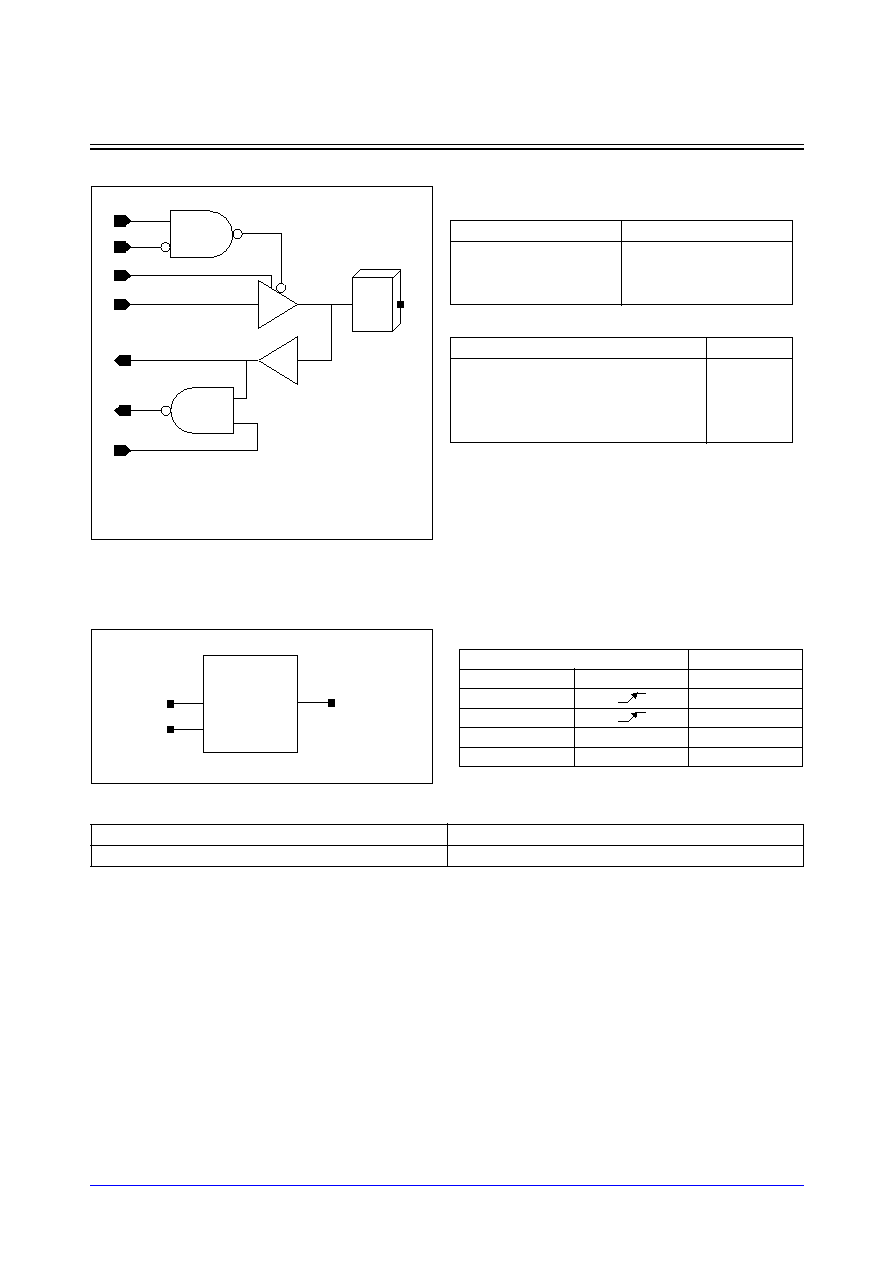
STDL130
4-146
Samsung ASIC
PTBPCI_LP
5V-Tolerant PCI Bi-directional Buffer
Logic Symbol
Option:
Voltage Detector for 3.3V or 5V Voltage Detecting.
Logic Symbol
Cell Data
Cell Name
Detecting Voltage
vdet_l130pci_lp
3.3V, 5V
Truth Table
Input Truth Table
Output Truth Table
PAD
PI
Y
PO
1
1
1
0
0
x
0
1
1
0
1
1
A
EN
TN
PAD
0
0
1
0
1
0
1
1
x
1
x
Hi-Z
x
x
0
Hi-Z
PAD
A
TN
EN
Y
PO
PI
EN5V
NOTE:
EN5V=Low: Enable the 5V signaling
EN5V=High: Enable the 3.3V signaling
Y
PD
A
Truth Table
Input
Output
A
PD
Y
3.3V
1
5V
0
X
0
Last Y
X
1
Last Y
Samsung ASIC
4-147
STDL130
POWER PADS
Cell List
Cell Type
Cell Name
Supply
Voltage
Description
Power
1.8V Interface Digital I/O
VDD1I_LP
1.8V
1.8V Internal
VDD1P_LP
1.8V
1.8V Pre-Driver
VDD1O_LP
1.8V
1.8V Output-Driver
VDD1IP_LP
1.8V
1.8V Internal and Pre-Driver
VDD1OP_LP
1.8V
1.8V Output-Driver and Pre-Driver
VDD1T_LP
1.8V
1.8V Total
2.5V Interface Digital I/O
VDD1IM_LP
1.8V
1.8V Internal for 2.5V Interface I/O
VDD2P_LP
2.5V
2.5V Pre-Driver
VDD2O_LP
2.5V
2.5V Output-Driver
VDD2OP_LP
2.5V
2.5V Output-Driver and Pre-Driver
3.3V Interface Digital I/O
VDD1IH_LP
1.8V
1.8V Internal for 3.3V Interface I/O
VDD3P_LP
3.3V
3.3V Pre-Driver
VDD3O_LP
3.3V
3.3V Output-Driver
VDD3OP_LP
3.3V
3.3V Output-Driver and Pre-Driver
Ground
1.8V Interface Digital I/O
VSS1I_LP
Internal GND for 1.8V Interface I/O
VSS1P_LP
Pre-Driver GND for 1.8V Interface I/O
VSS1O_LP
Output-Driver GND for 1.8V Interface I/O
VSS1IP_LP
Internal and Pre-Driver GND for 1.8V
Interface I/O
VSS1OP_LP
Output-Driver and Pre-Driver GND for
1.8V Interface I/O
VSS1T_LP
Total GND for 1.8V Interface I/O
2.5V Interface Digital I/O
VSS2I_LP
Internal GND for 2.5V Interface I/O
VSS2P_LP
Pre-Driver GND for 2.5V Interface I/O
VSS2O_LP
Output-Driver GND for 2.5V Interface I/O
VSS2IP_LP
Internal and Pre-Driver GND for 2.5V
Interface I/O
VSS2OP_LP
Output-Driver and Pre-Driver GND for
2.5V Interface I/O
VSS2T_LP
Total GND for 2.5V Interface I/O
3.3V Interface Digital I/O
VSS3I_LP
Internal GND for 3.3V Interface I/O
VSS3P_LP
Pre-Driver GND for 3.3V Interface I/O
VSS3O_LP
Output-Driver GND for 3.3V Interface I/O
VSS3IP_LP
Internal and Pre-Driver GND for 3.3V
Interface I/O
VSS3OP_LP
Output-Driver and Pre-Driver GND for
3.3V Interface I/O
VSS3T_LP
Total GND for 3.3V Interface I/O
STDL130
4-148
Samsung ASIC
POWER PADS
Cell List (Continued)
Cell Type
Cell Name
Supply
Voltage
Description
Power
1.8V Interface Analog I/O
VDD1I_ABB_LP
1.8V
1.8V Internal
VDD1OP_ABB_LP
1.8V
1.8V Output-Driver and Pre-Driver
VDD1T_ABB_LP
1.8V
1.8V Total
2.5V Interface Analog I/O
VDD1IM_ABB_LP
1.8V
1.8V Internal for 2.5V Interface I/O
VDD2I_ABB_LP
2.5V
2.5V Internal
VDD2OP_ABB_LP
2.5V
2.5V Output-Driver and Pre-Driver
VDD2T_ABB_LP
2.5V
2.5V Total
3.3V Interface Analog I/O
VDD1IH_ABB_LP
1.8V
1.8V Internal for 3.3V Interface I/O
VDD3I_ABB_LP
3.3V
3.3V Internal
VDD3OP_ABB_LP
3.3V
3.3V Output-Driver and Pre-Driver
VDD3T_ABB_LP
3.3V
3.3V Total
Ground
1.8V Interface Analog I/O
VSS1I_ABB_LP
Internal GND for 1.8V Interface I/O
VSS1OP_ABB_LP
Output-Driver and Pre-Driver GND for
1.8V Interface I/O
VSS1T_ABB_LP
Total GND for 1.8V Interface I/O
VBB1_ABB_LP
Bulk-Bias GND for 1.8V Interface I/O
VSS1BB_ABB_LP
Ground with VBB Ring Connected GND
for 1.8V Interface I/O
2.5V Interface Analog I/O
VSS2I_ABB_LP
Internal GND for 2.5V Interface I/O
VSS2OP_ABB_LP
Output-Driver and Pre-Driver GND for
2.5V Interface I/O
VSS2T_ABB_LP
Total GND for 2.5V Interface I/O
VBB2_ABB_LP
Bulk-Bias GND for 2.5V Interface I/O
VSS2BB_ABB_LP
Ground with VBB Ring Connected GND
for 2.5V Interface I/O
3.3V Interface Analog I/O
VSS3I_ABB_LP
Internal GND for 3.3V Interface I/O
VSS3OP_ABB_LP
Output-Driver and Pre-Driver GND for
3.3V Interface I/O
VSS3T_ABB_LP
Total GND for 3.3V Interface I/O
VBB3_ABB_LP
Bulk-Bias GND for 3.3V Interface I/O
VSS3BB_ABB_LP
Ground with VBB Ring Connected GND
for 3.3V Interface I/O
Samsung ASIC
4-149
STDL130
ANALOG INTERFACE
Analog Input
NOTE:
As to analog IO cells in the library, the voltage level of the input/output signal is the same as the IO power
supply voltage level, no level shifter inside.
Cell Name
Function Description
PIA_ABB_LP
Analog Normal Input Pad for 1.8V Interface with Separate Bulk Bias
PIAR10_ABB_LP
Analog Normal Input Pad for 1.8V Interface with Resistor 10ohm and Separate Bulk Bias
PIAR50_ABB_LP
Analog Normal Input Pad for 1.8V Interface with Resistor 50ohm and Separate Bulk Bias
PNC_ABB_LP
Analog No Connection Pad for 1.8V Interface with Separate Bulk Bias
PIC_ABB_LP
Analog CMOS Level Input Buffer for 1.8V Interface with Separate Bulk-Bias
PICC_ABB_LP
Analog CMOS Level Input Buffer for 1.8V Interface with Separate Bulk-Bias and without Nand-Tree
PICD_ABB_LP
Analog CMOS Level Input Buffer for 1.8V Interface with Pull-Down and Separate Bulk-Bias
PICEN_ABB_LP
Analog CMOS Level Input Buffer for 1.8V Interface with Enable Port and Separate Bulk-Bias
PICU_ABB_LP
Analog CMOS Level Input Buffer for 1.8V Interface with Pull-Up and Separate Bulk-Bias
PIS_ABB_LP
Analog CMOS Schmitt Trigger Level Input Buffer for 1.8V Interface with Separate Bulk Bias
PISD_ABB_LP
Analog CMOS Schmitt Trigger Level Input Buffer for 1.8V Interface with Pull-Down and Separate Bulk Bias
PISU_ABB_LP
Analog CMOS Schmitt Trigger Level Input Buffer for 1.8V Interface with Pull-Up and Separate Bulk Bias
PMIA_ABB_LP
Analog Normal Input Pad for 2.5V Interface with Separate Bulk Bias
PMIAR10_ABB_LP
Analog Normal Input Pad for 2.5V Interface with Resistor 10ohm and Separate Bulk Bias
PMIAR50_ABB_LP
Analog Normal Input Pad for 2.5V Interface with Resistor 50ohm and Separate Bulk Bias
PMNC_ABB_LP
Analog No Connection Pad for 2.5V Interface with Separate Bulk Bias
PMIC_ABB_LP
Analog CMOS Level Input Buffer for 2.5V Interface with Separate Bulk Bias
PMICC_ABB_LP
Analog CMOS Level Input Buffer for 2.5V Interface with Separate Bulk Bias and without Nand-Tree
PMICD_ABB_LP
Analog CMOS Level Input Buffer for 2.5V Interface with Pull-Down and Separate Bulk Bias
PMICEN_ABB_LP
Analog CMOS Level Input Buffer for 2.5V Interface with Enable Port and Separate Bulk Bias
PMICU_ABB_LP
Analog CMOS Level Input Buffer for 2.5V Interface with Pull-Up and Separate Bulk Bias
PMIS_ABB_LP
Analog CMOS Schmitt Trigger Level Input Buffer for 2.5V Interface with Separate Bulk Bias
PMISD_ABB_LP
Analog CMOS Schmitt Trigger Level Input Buffer for 2.5V Interface with Pull-Down and Separate Bulk Bias
PMISU_ABB_LP
Analog CMOS Schmitt Trigger Level Input Buffer for 2.5V Interface with Pull-Up and Separate Bulk Bias
PHIA_ABB_LP
Analog Normal Input Pad for 3.3V Interface with Separate Bulk Bias
PHIAR10_ABB_LP
Analog Normal Input Pad for 3.3V Interface with Resistor 10ohm and Separate Bulk Bias
PHIAR50_ABB_LP
Analog Normal Input Pad for 3.3V Interface with Resistor 50ohm and Separate Bulk Bias
PHNC_ABB_LP
Analog No Connection Pad for 3.3V Interface with Separate Bulk Bias
PHIC_ABB_LP
Analog LVCMOS Level Input Buffer for 3.3V Interface with Separate Bulk-Bias
PHICC_ABB_LP
Analog LVCMOS Level Input Buffer for 3.3V Interface with Separate Bulk-Bias and without Nand-Tree
PHICD_ABB_LP
Analog LVCMOS Level Input Buffer for 3.3V Interface with Pull-Down and Separate Bulk-Bias
PHICEN_ABB_LP
Analog LVCMOS Level Input Buffer for 3.3V Interface with Enable Port and Separate Bulk-Bias
PHICU_ABB_LP
Analog LVCMOS Level Input Buffer for 3.3V Interface with Pull-Up and Separate Bulk-Bias
PHIS_ABB_LP
Analog LVCMOS Schmitt Trigger Level Input Buffer for 3.3V Interface with Separated Bulk Bias
PHISD_ABB_LP
Analog LVCMOS Schmitt Trigger Level Input Buffer for 3.3V Interface with Pull-Down and Separate Bulk
Bias
PHISU_ABB_LP
Analog LVCMOS Schmitt Trigger Level Input Buffer for 3.3V Interface with Pull-Up and Separate Bulk Bias

STDL130
4-150
Samsung ASIC
ANALOG INTERFACE
Analog Output
Analog Bi-Direction
NOTE:
As to analog IO cells in the library, the voltage level of the input/output signal is the same as the IO power
supply voltage level, no level shifter inside.
Cell Name
Function Description
POA_ABB_LP
Analog Normal Output Pad for 1.8V Interface with Separate Bulk Bias
POAR10_ABB_LP
Analog Normal Output Pad for 1.8V Interface with Resistor 10ohm and
Separate Bulk Bias
POAR50_ABB_LP
Analog Normal Output Pad for 1.8V Interface with Resistor 50ohm and
Separate Bulk Bias
POB1/2/8_ABB_LP
Analog Normal Output Buffer for 1.8V Interface with Separate Bulk Bias,
1/2/8mA Drive
POT1/2/4/6/8/10/12/16_ABB_LP
Analog Tri-State Output Buffer for 1.8V Interface with Separate Bulk Bias,
1/2/4/6/8/10/12/16mA Drive
PMOA_ABB_LP
Analog Normal Output Pad for 2.5V Interface with Separate Bulk Bias
PMOAR10_ABB_LP
Analog Normal Output Pad for 2.5V Interface with Resistor 10ohm and
Separate Bulk Bias
PMOAR50_ABB_LP
Analog Normal Output Pad for 2.5V Interface with Resistor 50ohm and
Separate Bulk Bias
PMOB1/2/8_ABB_LP
Analog Normal Output Buffer for 2.5V Interface with Separate Bulk Bias,
1/2/8mA Drive
PMOT1/2/4/6/8/10/12/16_ABB_LP
Analog Tri-State Output Buffer for 2.5V Interface with Separate Bulk Bias,
1/2/4/6/8/10/12/16mA Drive
PHOA_ABB_LP
Analog Normal Output Pad for 3.3V Interface with Separate Bulk Bias
PHOAR10_ABB_LP
Analog Normal Output Pad for 3.3V Interface with Resistor 10ohm and
Separate Bulk Bias
PHOAR50_ABB_LP
Analog Normal Output Pad for 3.3V Interface with Resistor 50ohm and
Separate Bulk Bias
PHOB1/2/8_ABB_LP
Analog Normal Output Buffer for 3.3V Interface with Separate Bulk Bias,
1/2/8mA Drive
PHOT1/2/4/6/8/10/12/16_ABB_LP
Analog Tri-State Output Buffer for 3.3V Interface with Separate Bulk Bias,
1/2/4/6/8/10/12/16mA Drive
PHOD4SM_ABB_LP
Analog Open-Drain Output Buffer for 3.3V Interface with Separated Bulk
Bias, 4mA Drive
Cell Name
Function Description
PBCT1/2/4/6_ABB_LP
Analog Bi-Directional Buffer for 1.8V Interface with CMOS Level Input,
Tri-State Output Pad with Separate Bulk Bias, 1/2/4/6mA Drive
PMBCT1/2/4/6_ABB_LP
Analog Bi-Directional Buffer for 2.5V Interface with CMOS Level Input,
Tri-State Output Pad with Separate Bulk Bias, 1/2/4/6mA Drive
PHBCT1/2/4/6_ABB_LP
Analog Bi-Directional Buffer for 3.3V Interface with CMOS Level Input,
Tri-State Output Pad with Separate Bulk Bias, 1/2/4/6mA Drive
PHBSD4SM_ABB_LP
Analog Bi-Directional Buffer for 3.3V Interface with CMOS Schmitt Trigger
Lever Input, Open-Drain Output Pad with Separated Bulk Bias, 4mA Drive
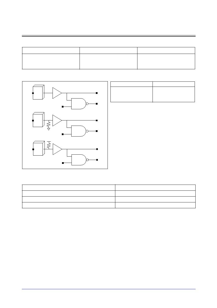
Samsung ASIC
4-151
STDL130
PvIC_ABB_LP/PvICD_ABB_LP/PvICU_ABB_LP
Analog CMOS Level Input Buffers with Separate Bulk-Bias
Cell Availability
Logic Symbol
Standard Load (SL)
1.8V Only
2.5V Interface
3.3V Interface
PIC_ABB_LP
PICD_ABB_LP
PICU_ABB_LP
PMIC_ABB_LP
PMICD_ABB_LP
PMICU_ABB_LP
PHIC_ABB_LP
PHICD_ABB_LP
PHICU_ABB_LP
Cell Name
PI
PIC_ABB_LP/PICD_ABB_LP/PICU_ABB_LP
3.79
PMIC_ABB_LP/PMICD_ABB_LP/PMICU_ABB_LP
2.13
PHIC_ABB_LP/PHICD_ABB_LP/PHICU_ABB_LP
2.33
Truth Table
PAD
PI
Y
PO
1
1
1
0
0
x
0
1
1
0
1
1
Y
PO
PI
PAD
Y
PO
PI
PAD
Y
PO
PI
PAD
PvIC_ABB_LP
PvICD_ABB_LP
PvICU_ABB_LP
STDL130
4-152
Samsung ASIC
PvIC_ABB_LP/PvICD_ABB_LP/PvICU_ABB_LP
Analog CMOS Level Input Buffers with Separate Bulk-Bias
Switching Characteristics
(Typical process, 25
∞
C, 1.8V, t
R
/t
F
= 1.50ns, SL: Standard Load)
PIC_ABB_LP
PICD_ABB_LP
PICU_ABB_LP
Path
Parameter
Delay [ns]
SL = 2
Delay Equations [ns]
Group1*
Group2*
Group3*
PAD to Y
tR
0.120
0.112 + 0.004*SL
0.112 + 0.004*SL
0.110 + 0.004*SL
tF
0.106
0.098 + 0.004*SL
0.098 + 0.004*SL
0.091 + 0.004*SL
tPLH
0.388
0.380 + 0.004*SL
0.385 + 0.003*SL
0.402 + 0.002*SL
tPHL
0.383
0.375 + 0.004*SL
0.379 + 0.003*SL
0.393 + 0.002*SL
*Group1 : SL < 4, *Group2 : 4 SL
<
<
=
= 27, *Group3 : 27 < SL
Path
Parameter
Delay [ns]
SL = 2
Delay Equations [ns]
Group1*
Group2*
Group3*
PAD to Y
tR
0.119
0.111 + 0.004*SL
0.111 + 0.004*SL
0.109 + 0.004*SL
tF
0.107
0.098 + 0.004*SL
0.100 + 0.004*SL
0.091 + 0.004*SL
tPLH
0.412
0.404 + 0.004*SL
0.409 + 0.003*SL
0.426 + 0.002*SL
tPHL
0.377
0.369 + 0.004*SL
0.373 + 0.003*SL
0.387 + 0.002*SL
*Group1 : SL < 4, *Group2 : 4 SL
<
<
=
= 27, *Group3 : 27 < SL
Path
Parameter
Delay [ns]
SL = 2
Delay Equations [ns]
Group1*
Group2*
Group3*
PAD to Y
tR
0.120
0.111 + 0.004*SL
0.114 + 0.004*SL
0.109 + 0.004*SL
tF
0.105
0.097 + 0.004*SL
0.098 + 0.004*SL
0.090 + 0.004*SL
tPLH
0.378
0.370 + 0.004*SL
0.374 + 0.003*SL
0.392 + 0.002*SL
tPHL
0.400
0.391 + 0.004*SL
0.396 + 0.003*SL
0.410 + 0.002*SL
*Group1 : SL < 4, *Group2 : 4 SL
<
<
=
= 27, *Group3 : 27 < SL

Samsung ASIC
4-153
STDL130
PvIC_ABB_LP/PvICD_ABB_LP/PvICU_ABB_LP
Analog CMOS Level Input Buffers with Separate Bulk-Bias
Switching Characteristics
(Typical process, 25
∞
C, 2.5V, t
R
/t
F
= 1.50ns, SL: Standard Load)
PMIC_ABB_LP
PMICD_ABB_LP
PMICU_ABB_LP
Path
Parameter
Delay [ns]
SL = 2
Delay Equations [ns]
Group1*
Group2*
Group3*
PAD to Y
tR
0.142
0.128 + 0.007*SL
0.133 + 0.006*SL
0.127 + 0.006*SL
tF
0.122
0.109 + 0.006*SL
0.112 + 0.006*SL
0.111 + 0.006*SL
tPLH
0.428
0.417 + 0.006*SL
0.424 + 0.004*SL
0.446 + 0.003*SL
tPHL
0.453
0.442 + 0.006*SL
0.448 + 0.004*SL
0.470 + 0.003*SL
*Group1 : SL < 4, *Group2 : 4 SL
<
<
=
= 27, *Group3 : 27 < SL
Path
Parameter
Delay [ns]
SL = 2
Delay Equations [ns]
Group1*
Group2*
Group3*
PAD to Y
tR
0.141
0.128 + 0.007*SL
0.132 + 0.006*SL
0.126 + 0.006*SL
tF
0.124
0.110 + 0.007*SL
0.115 + 0.005*SL
0.113 + 0.006*SL
tPLH
0.444
0.433 + 0.006*SL
0.440 + 0.004*SL
0.462 + 0.003*SL
tPHL
0.450
0.438 + 0.006*SL
0.444 + 0.004*SL
0.467 + 0.003*SL
*Group1 : SL < 4, *Group2 : 4 SL
<
<
=
= 27, *Group3 : 27 < SL
Path
Parameter
Delay [ns]
SL = 2
Delay Equations [ns]
Group1*
Group2*
Group3*
PAD to Y
tR
0.143
0.130 + 0.006*SL
0.133 + 0.006*SL
0.127 + 0.006*SL
tF
0.121
0.108 + 0.007*SL
0.113 + 0.005*SL
0.110 + 0.006*SL
tPLH
0.420
0.409 + 0.006*SL
0.416 + 0.004*SL
0.438 + 0.003*SL
tPHL
0.468
0.456 + 0.006*SL
0.463 + 0.004*SL
0.484 + 0.003*SL
*Group1 : SL < 4, *Group2 : 4 SL
<
<
=
= 27, *Group3 : 27 < SL
STDL130
4-154
Samsung ASIC
PvIC_ABB_LP/PvICD_ABB_LP/PvICU_ABB_LP
Analog CMOS Level Input Buffers with Separate Bulk-Bias
Switching Characteristics
(Typical process, 25
∞
C, 3.3V, t
R
/t
F
= 1.50ns, SL: Standard Load)
PHIC_ABB_LP
PHICD_ABB_LP
PHICU_ABB_LP
Path
Parameter
Delay [ns]
SL = 2
Delay Equations [ns]
Group1*
Group2*
Group3*
PAD to Y
tR
0.118
0.108 + 0.005*SL
0.110 + 0.004*SL
0.104 + 0.005*SL
tF
0.109
0.099 + 0.005*SL
0.100 + 0.005*SL
0.102 + 0.005*SL
tPLH
0.174
0.166 + 0.004*SL
0.171 + 0.003*SL
0.185 + 0.002*SL
tPHL
0.495
0.486 + 0.004*SL
0.490 + 0.003*SL
0.506 + 0.003*SL
*Group1 : SL < 4, *Group2 : 4 SL
<
<
=
= 27, *Group3 : 27 < SL
Path
Parameter
Delay [ns]
SL = 2
Delay Equations [ns]
Group1*
Group2*
Group3*
PAD to Y
tR
0.116
0.106 + 0.005*SL
0.109 + 0.004*SL
0.102 + 0.005*SL
tF
0.112
0.101 + 0.005*SL
0.104 + 0.005*SL
0.103 + 0.005*SL
tPLH
0.198
0.190 + 0.004*SL
0.194 + 0.003*SL
0.208 + 0.002*SL
tPHL
0.504
0.495 + 0.004*SL
0.499 + 0.003*SL
0.516 + 0.003*SL
*Group1 : SL < 4, *Group2 : 4 SL
<
<
=
= 27, *Group3 : 27 < SL
Path
Parameter
Delay [ns]
SL = 2
Delay Equations [ns]
Group1*
Group2*
Group3*
PAD to Y
tR
0.120
0.110 + 0.005*SL
0.112 + 0.004*SL
0.106 + 0.005*SL
tF
0.110
0.100 + 0.005*SL
0.101 + 0.005*SL
0.102 + 0.005*SL
tPLH
0.165
0.157 + 0.004*SL
0.162 + 0.003*SL
0.176 + 0.002*SL
tPHL
0.510
0.501 + 0.004*SL
0.505 + 0.003*SL
0.521 + 0.003*SL
*Group1 : SL < 4, *Group2 : 4 SL
<
<
=
= 27, *Group3 : 27 < SL
Samsung ASIC
4-155
STDL130
PICC_ABB_LP/PMICC_ABB_LP/PHICC_ABB_LP
Analog CMOS Level Input Buffers with Separate Bulk-Bias
Logic Symbol
Switching Characteristics
(Typical process, 25
∞
C, 1.8V, t
R
/t
F
= 1.50ns, SL: Standard Load)
PICC_ABB_LP
(Typical process, 25
∞
C, 2.5V, t
R
/t
F
= 1.50ns, SL: Standard Load)
PMICC_ABB_LP
(Typical process, 25
∞
C, 3.3V, t
R
/t
F
= 1.50ns, SL: Standard Load)
PHICC_ABB_LP
Truth Table
PAD
Y
0
0
1
1
Y
PAD
Path
Parameter
Delay [ns]
SL = 2
Delay Equations [ns]
Group1*
Group2*
Group3*
PAD to Y
tR
0.105
0.096 + 0.005*SL
0.099 + 0.004*SL
0.092 + 0.004*SL
tF
0.091
0.082 + 0.005*SL
0.085 + 0.004*SL
0.076 + 0.004*SL
tPLH
0.373
0.363 + 0.005*SL
0.370 + 0.003*SL
0.393 + 0.002*SL
tPHL
0.370
0.361 + 0.005*SL
0.367 + 0.003*SL
0.385 + 0.002*SL
*Group1 : SL < 4, *Group2 : 4 SL
<
<
=
= 27, *Group3 : 27 < SL
Path
Parameter
Delay [ns]
SL = 2
Delay Equations [ns]
Group1*
Group2*
Group3*
PAD to Y
tR
0.130
0.115 + 0.007*SL
0.122 + 0.006*SL
0.114 + 0.006*SL
tF
0.110
0.096 + 0.007*SL
0.102 + 0.006*SL
0.100 + 0.006*SL
tPLH
0.419
0.407 + 0.006*SL
0.415 + 0.004*SL
0.440 + 0.003*SL
tPHL
0.444
0.432 + 0.006*SL
0.439 + 0.004*SL
0.464 + 0.003*SL
*Group1 : SL < 4, *Group2 : 4 SL
<
<
=
= 27, *Group3 : 27 < SL
Path
Parameter
Delay [ns]
SL = 2
Delay Equations [ns]
Group1*
Group2*
Group3*
PAD to Y
tR
0.109
0.099 + 0.005*SL
0.101 + 0.004*SL
0.094 + 0.005*SL
tF
0.099
0.089 + 0.005*SL
0.090 + 0.005*SL
0.091 + 0.005*SL
tPLH
0.167
0.158 + 0.004*SL
0.164 + 0.003*SL
0.180 + 0.002*SL
tPHL
0.486
0.477 + 0.005*SL
0.482 + 0.004*SL
0.501 + 0.003*SL
*Group1 : SL < 4, *Group2 : 4 SL
<
<
=
= 27, *Group3 : 27 < SL
STDL130
4-156
Samsung ASIC
PICEN_ABB_LP/PMICEN_ABB_LP/PHICEN_ABB_LP
Analog CMOS Level Input Buffers with Enable Port and Separate Bulk-Bias
Cell Availability
Logic Symbol
Standard Load (SL)
Switching Characteristics
(Typical process, 25
∞
C, 1.8V, t
R
/t
F
= 1.50ns, SL: Standard Load)
PICEN_ABB_LP
1.8V Only
2.5V Interface
3.3V Interface
PICEN_ABB_LP
PMICEN_ABB_LP
PHICEN_ABB_LP
Cell Name
PI
EN
PICEN_ABB_LP
3.79
3.80
PMICEN_ABB_LP
2.13
2.46
PHICEN_ABB_LP
2.33
2.40
Truth Table
PAD
PI
EN
Y
PO
1
1
1
1
0
0
x
1
0
1
1
0
1
1
1
x
x
0
0
1
Y
PO
PI
PAD
EN
Path
Parameter
Delay [ns]
SL = 2
Delay Equations [ns]
Group1*
Group2*
Group3*
PAD to Y
tR
0.118
0.108 + 0.005*SL
0.111 + 0.004*SL
0.107 + 0.004*SL
tF
0.109
0.101 + 0.004*SL
0.102 + 0.004*SL
0.098 + 0.004*SL
tPLH
0.318
0.310 + 0.004*SL
0.315 + 0.003*SL
0.332 + 0.002*SL
tPHL
0.451
0.443 + 0.004*SL
0.447 + 0.003*SL
0.465 + 0.002*SL
EN to Y
tR
0.081
0.072 + 0.004*SL
0.072 + 0.004*SL
0.073 + 0.004*SL
tF
0.072
0.064 + 0.004*SL
0.063 + 0.004*SL
0.062 + 0.004*SL
tPLH
0.177
0.171 + 0.003*SL
0.173 + 0.003*SL
0.182 + 0.002*SL
tPHL
0.200
0.193 + 0.003*SL
0.196 + 0.003*SL
0.204 + 0.002*SL
*Group1 : SL < 4, *Group2 : 4 SL
<
<
=
= 27, *Group3 : 27 < SL

Samsung ASIC
4-157
STDL130
PICEN_ABB_LP/PMICEN_ABB_LP/PHICEN_ABB_LP
Analog CMOS Level Input Buffers with Enable Port and Separate Bulk-Bias
Switching Characteristics
(Typical process, 25
∞
C, 2.5V, t
R
/t
F
= 1.50ns, SL: Standard Load)
PMICEN_ABB_LP
(Typical process, 25
∞
C, 3.3V, t
R
/t
F
= 1.50ns, SL: Standard Load)
PHICEN_ABB_LP
Path
Parameter
Delay [ns]
SL = 2
Delay Equations [ns]
Group1*
Group2*
Group3*
PAD to Y
tR
0.163
0.147 + 0.008*SL
0.155 + 0.006*SL
0.162 + 0.006*SL
tF
0.137
0.122 + 0.007*SL
0.128 + 0.006*SL
0.133 + 0.006*SL
tPLH
0.541
0.529 + 0.006*SL
0.536 + 0.005*SL
0.566 + 0.003*SL
tPHL
0.539
0.526 + 0.006*SL
0.533 + 0.005*SL
0.561 + 0.004*SL
EN to Y
tR
0.130
0.116 + 0.007*SL
0.119 + 0.006*SL
0.128 + 0.006*SL
tF
0.101
0.088 + 0.006*SL
0.090 + 0.006*SL
0.094 + 0.006*SL
tPLH
0.293
0.282 + 0.006*SL
0.288 + 0.004*SL
0.313 + 0.003*SL
tPHL
0.289
0.278 + 0.006*SL
0.284 + 0.004*SL
0.304 + 0.003*SL
*Group1 : SL < 4, *Group2 : 4 SL
<
<
=
= 27, *Group3 : 27 < SL
Path
Parameter
Delay [ns]
SL = 2
Delay Equations [ns]
Group1*
Group2*
Group3*
PAD to Y
tR
0.138
0.128 + 0.005*SL
0.131 + 0.004*SL
0.130 + 0.004*SL
tF
0.133
0.122 + 0.006*SL
0.125 + 0.005*SL
0.129 + 0.005*SL
tPLH
0.273
0.265 + 0.004*SL
0.270 + 0.003*SL
0.288 + 0.002*SL
tPHL
0.577
0.568 + 0.005*SL
0.572 + 0.004*SL
0.593 + 0.003*SL
EN to Y
tR
0.088
0.078 + 0.005*SL
0.080 + 0.005*SL
0.082 + 0.005*SL
tF
0.103
0.092 + 0.006*SL
0.094 + 0.005*SL
0.100 + 0.005*SL
tPLH
0.167
0.160 + 0.004*SL
0.163 + 0.003*SL
0.175 + 0.002*SL
tPHL
0.292
0.283 + 0.005*SL
0.287 + 0.004*SL
0.305 + 0.003*SL
*Group1 : SL < 4, *Group2 : 4 SL
<
<
=
= 27, *Group3 : 27 < SL
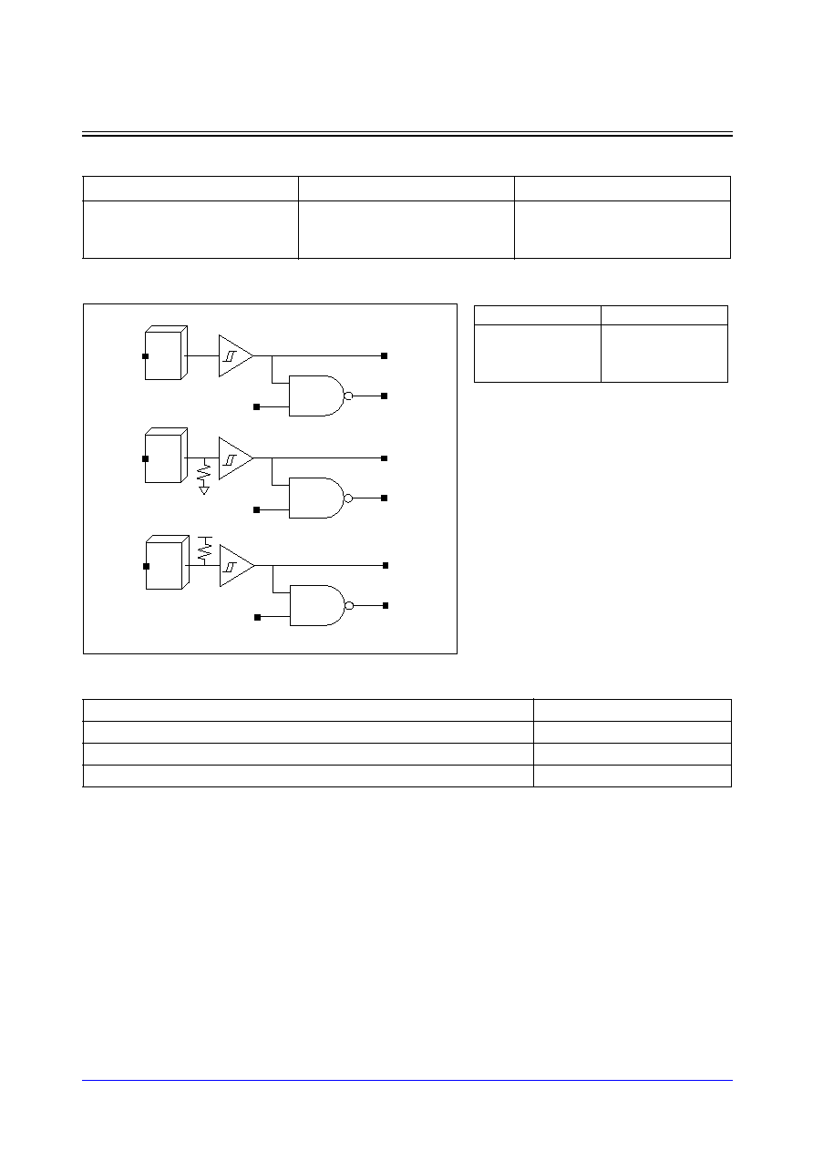
STDL130
4-158
Samsung ASIC
PvIS_ABB_LP/PvISD_ABB_LP/PvISU_ABB_LP
Analog CMOS Schmitt Trigger Level Input Buffer with Separate Bulk-Bias
Cell Availability
Logic Symbol
Standard Load (SL)
1.8V Only
2.5V Interface
3.3V Interface
PIS_ABB_LP
PISD_ABB_LP
PISU_ABB_LP
PMIS_ABB_LP
PMISD_ABB_LP
PMISU_ABB_LP
PHIS_ABB_LP
PHISD_ABB_LP
PHISU_ABB_LP
Cell Name
PI
PIS_ABB_LP/PISD_ABB_LP/PISU_ABB_LP
3.79
PMIS_ABB_LP/PMISD_ABB_LP/PMISU_ABB_LP
2.13
PHIS_ABB_LP/PHISD_ABB_LP/PHISU_ABB_LP
2.33
Truth Table
PAD
PI
Y
PO
1
1
1
0
0
x
0
1
1
0
1
1
Y
PO
PI
PAD
Y
PO
PI
PAD
Y
PO
PI
PAD
PvIS_ABB_LP
PvISD_ABB_LP
PvISU_ABB_LP

Samsung ASIC
4-159
STDL130
PvIS_ABB_LP/PvISD_ABB_LP/PvISU_ABB_LP
Analog CMOS Schmitt Trigger Level Input Buffer with Separate Bulk-Bias
Switching Characteristics
(Typical process, 25
∞
C, 1.8V, t
R
/t
F
= 1.50ns, SL: Standard Load)
PIS_ABB_LP
PISD_ABB_LP
PISU_ABB_LP
Path
Parameter
Delay [ns]
SL = 2
Delay Equations [ns]
Group1*
Group2*
Group3*
PAD to Y
tR
0.113
0.103 + 0.005*SL
0.106 + 0.004*SL
0.107 + 0.004*SL
tF
0.121
0.112 + 0.005*SL
0.114 + 0.004*SL
0.119 + 0.004*SL
tPLH
0.653
0.645 + 0.004*SL
0.650 + 0.003*SL
0.667 + 0.002*SL
tPHL
0.688
0.679 + 0.005*SL
0.684 + 0.003*SL
0.704 + 0.003*SL
*Group1 : SL < 4, *Group2 : 4 SL
<
<
=
= 27, *Group3 : 27 < SL
Path
Parameter
Delay [ns]
SL = 2
Delay Equations [ns]
Group1*
Group2*
Group3*
PAD to Y
tR
0.115
0.105 + 0.005*SL
0.108 + 0.004*SL
0.109 + 0.004*SL
tF
0.124
0.115 + 0.005*SL
0.117 + 0.004*SL
0.121 + 0.004*SL
tPLH
0.656
0.648 + 0.004*SL
0.652 + 0.003*SL
0.671 + 0.002*SL
tPHL
0.695
0.686 + 0.005*SL
0.691 + 0.003*SL
0.712 + 0.003*SL
*Group1 : SL < 4, *Group2 : 4 SL
<
<
=
= 27, *Group3 : 27 < SL
Path
Parameter
Delay [ns]
SL = 2
Delay Equations [ns]
Group1*
Group2*
Group3*
PAD to Y
tR
0.114
0.104 + 0.005*SL
0.106 + 0.004*SL
0.108 + 0.004*SL
tF
0.122
0.111 + 0.005*SL
0.115 + 0.004*SL
0.119 + 0.004*SL
tPLH
0.658
0.650 + 0.004*SL
0.654 + 0.003*SL
0.673 + 0.002*SL
tPHL
0.703
0.694 + 0.005*SL
0.699 + 0.003*SL
0.720 + 0.003*SL
*Group1 : SL < 4, *Group2 : 4 SL
<
<
=
= 27, *Group3 : 27 < SL

STDL130
4-160
Samsung ASIC
PvIS_ABB_LP/PvISD_ABB_LP/PvISU_ABB_LP
Analog CMOS Schmitt Trigger Level Input Buffer with Separate Bulk-Bias
Switching Characteristics
(Typical process, 25
∞
C, 2.5V, t
R
/t
F
= 1.50ns, SL: Standard Load)
PMIS_ABB_LP
PMISD_ABB_LP
PMISU_ABB_LP
Path
Parameter
Delay [ns]
SL = 2
Delay Equations [ns]
Group1*
Group2*
Group3*
PAD to Y
tR
0.111
0.099 + 0.006*SL
0.099 + 0.006*SL
0.096 + 0.006*SL
tF
0.120
0.104 + 0.008*SL
0.111 + 0.006*SL
0.125 + 0.006*SL
tPLH
0.600
0.590 + 0.005*SL
0.595 + 0.004*SL
0.610 + 0.003*SL
tPHL
0.862
0.850 + 0.006*SL
0.856 + 0.005*SL
0.885 + 0.004*SL
*Group1 : SL < 4, *Group2 : 4 SL
<
<
=
= 27, *Group3 : 27 < SL
Path
Parameter
Delay [ns]
SL = 2
Delay Equations [ns]
Group1*
Group2*
Group3*
PAD to Y
tR
0.111
0.097 + 0.007*SL
0.100 + 0.006*SL
0.097 + 0.006*SL
tF
0.121
0.105 + 0.008*SL
0.112 + 0.006*SL
0.126 + 0.006*SL
tPLH
0.606
0.596 + 0.005*SL
0.601 + 0.004*SL
0.616 + 0.003*SL
tPHL
0.883
0.870 + 0.006*SL
0.876 + 0.005*SL
0.905 + 0.004*SL
*Group1 : SL < 4, *Group2 : 4 SL
<
<
=
= 27, *Group3 : 27 < SL
Path
Parameter
Delay [ns]
SL = 2
Delay Equations [ns]
Group1*
Group2*
Group3*
PAD to Y
tR
0.110
0.096 + 0.007*SL
0.099 + 0.006*SL
0.096 + 0.006*SL
tF
0.121
0.106 + 0.008*SL
0.112 + 0.006*SL
0.125 + 0.006*SL
tPLH
0.605
0.595 + 0.005*SL
0.599 + 0.004*SL
0.614 + 0.003*SL
tPHL
0.870
0.857 + 0.006*SL
0.863 + 0.005*SL
0.892 + 0.004*SL
*Group1 : SL < 4, *Group2 : 4 SL
<
<
=
= 27, *Group3 : 27 < SL

Samsung ASIC
4-161
STDL130
PvIS_ABB_LP/PvISD_ABB_LP/PvISU_ABB_LP
Analog CMOS Schmitt Trigger Level Input Buffer with Separate Bulk-Bias
Switching Characteristics
(Typical process, 25
∞
C, 3.3V, t
R
/t
F
= 1.50ns, SL: Standard Load)
PHIS_ABB_LP
PHISD_ABB_LP
PHISU_ABB_LP
Path
Parameter
Delay [ns]
SL = 2
Delay Equations [ns]
Group1*
Group2*
Group3*
PAD to Y
tR
0.088
0.079 + 0.005*SL
0.079 + 0.005*SL
0.077 + 0.005*SL
tF
0.106
0.094 + 0.006*SL
0.097 + 0.005*SL
0.106 + 0.005*SL
tPLH
0.411
0.404 + 0.003*SL
0.407 + 0.003*SL
0.416 + 0.002*SL
tPHL
0.832
0.822 + 0.005*SL
0.826 + 0.004*SL
0.845 + 0.003*SL
*Group1 : SL < 4, *Group2 : 4 SL
<
<
=
= 27, *Group3 : 27 < SL
Path
Parameter
Delay [ns]
SL = 2
Delay Equations [ns]
Group1*
Group2*
Group3*
PAD to Y
tR
0.093
0.083 + 0.005*SL
0.085 + 0.005*SL
0.080 + 0.005*SL
tF
0.106
0.095 + 0.005*SL
0.096 + 0.005*SL
0.105 + 0.005*SL
tPLH
0.426
0.419 + 0.004*SL
0.422 + 0.003*SL
0.433 + 0.002*SL
tPHL
0.865
0.856 + 0.005*SL
0.860 + 0.004*SL
0.879 + 0.003*SL
*Group1 : SL < 4, *Group2 : 4 SL
<
<
=
= 27, *Group3 : 27 < SL
Path
Parameter
Delay [ns]
SL = 2
Delay Equations [ns]
Group1*
Group2*
Group3*
PAD to Y
tR
0.099
0.089 + 0.005*SL
0.091 + 0.005*SL
0.089 + 0.005*SL
tF
0.106
0.095 + 0.006*SL
0.098 + 0.005*SL
0.106 + 0.005*SL
tPLH
0.422
0.414 + 0.004*SL
0.418 + 0.003*SL
0.430 + 0.002*SL
tPHL
0.862
0.852 + 0.005*SL
0.856 + 0.004*SL
0.876 + 0.003*SL
*Group1 : SL < 4, *Group2 : 4 SL
<
<
=
= 27, *Group3 : 27 < SL
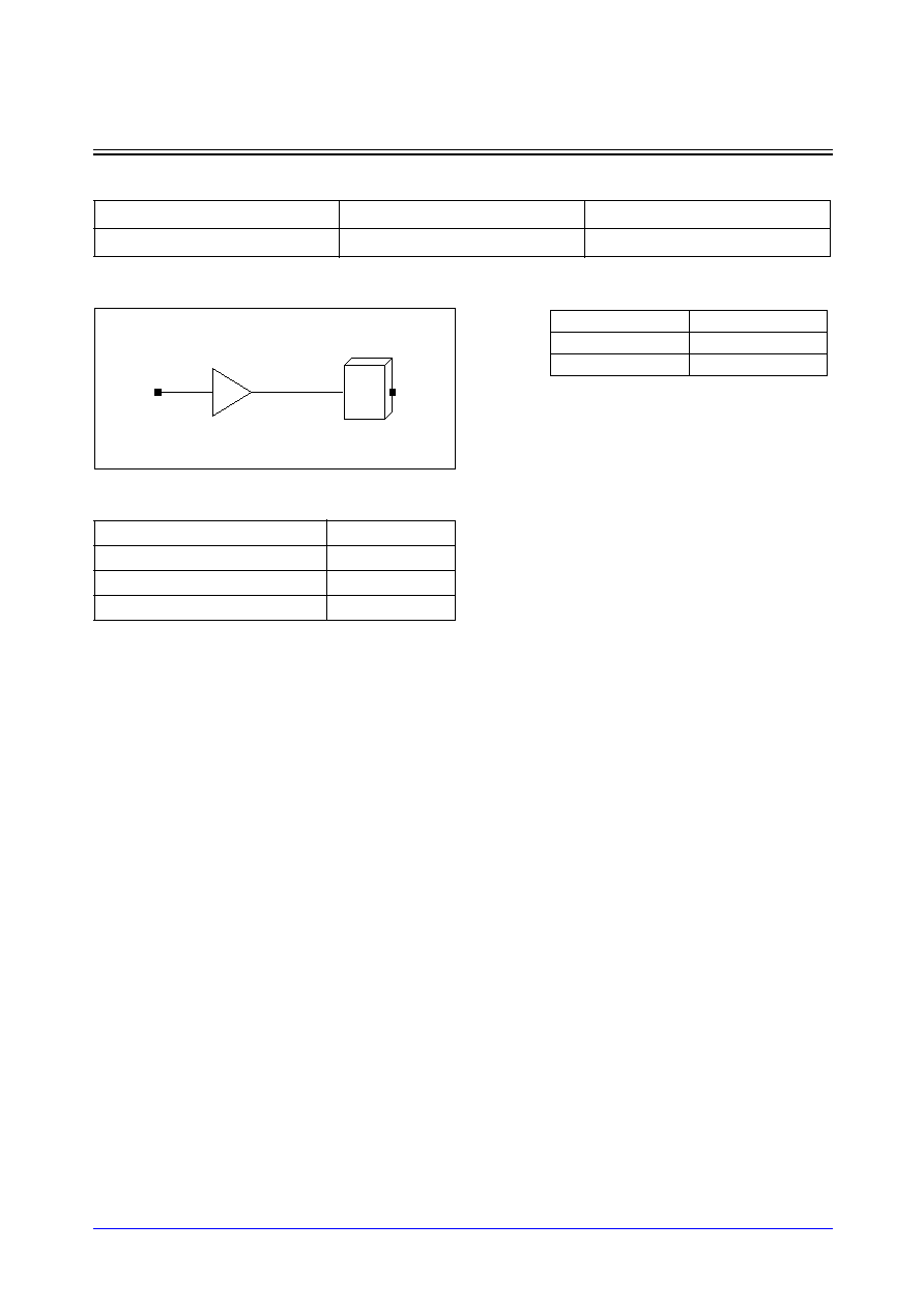
STDL130
4-162
Samsung ASIC
PvOByz_ABB_LP
Analog Normal Output Buffers with Separate Bulk-Bias
Cell Availability
Logic Symbol
Standard Load (SL)
1.8V Only
2.5V Interface
3.3V Interface
POB(1/2/8)_ABB_LP
PMOB(1/2/8)_ABB_LP
PHOB(1/2/8)_ABB_LP
Cell Name
A
POB(1/2/8)_ABB_LP
15.95
PMOB(1/2/8)_ABB_LP
10.47
PHOB(1/2/8)_ABB_LP
12.09
Truth Table
A
PAD
0
0
1
1
A
PAD
Samsung ASIC
4-163
STDL130
PvOB1/2/8_ABB_LP
Analog Normal Output Buffers with Separate Bulk-Bias
Switching Characteristics
(Typical process, 25
∞
C, 1.8V, t
R
/t
F
= 0.20ns, CL: Capacitive Load[pF])
POB1_ABB_LP
POB2_ABB_LP
POB8_ABB_LP
Path
Parameter
Delay [ns]
CL = 50.0pF
Delay Equations [ns]
Group1*
Group2*
Group3*
A to PAD
tR
20.215
1.333 + 0.378*CL
1.329 + 0.378*CL
1.326 + 0.378*CL
tF
22.775
1.555 + 0.424*CL
1.547 + 0.425*CL
1.541 + 0.425*CL
tPLH
9.705
0.791 + 0.178*CL
0.790 + 0.178*CL
0.791 + 0.178*CL
tPHL
12.279
1.412 + 0.217*CL
1.413 + 0.217*CL
1.410 + 0.217*CL
*Group1 : CL < 50, *Group2 : 50 CL
<
<
=
= 75, *Group3 : 75 < CL
Path
Parameter
Delay [ns]
CL = 50.0pF
Delay Equations [ns]
Group1*
Group2*
Group3*
A to PAD
tR
13.606
0.929 + 0.254*CL
0.928 + 0.254*CL
0.925 + 0.254*CL
tF
12.068
0.834 + 0.225*CL
0.830 + 0.225*CL
0.821 + 0.225*CL
tPLH
6.770
0.701 + 0.121*CL
0.702 + 0.121*CL
0.703 + 0.121*CL
tPHL
6.674
0.821 + 0.117*CL
0.823 + 0.117*CL
0.822 + 0.117*CL
*Group1 : CL < 50, *Group2 : 50 CL
<
<
=
= 75, *Group3 : 75 < CL
Path
Parameter
Delay [ns]
CL = 50.0pF
Delay Equations [ns]
Group1*
Group2*
Group3*
A to PAD
tR
3.401
0.254 + 0.063*CL
0.254 + 0.063*CL
0.254 + 0.063*CL
tF
3.423
0.255 + 0.063*CL
0.254 + 0.063*CL
0.253 + 0.063*CL
tPLH
1.857
0.368 + 0.030*CL
0.370 + 0.030*CL
0.371 + 0.030*CL
tPHL
2.089
0.381 + 0.034*CL
0.382 + 0.034*CL
0.383 + 0.034*CL
*Group1 : CL < 50, *Group2 : 50 CL
<
<
=
= 75, *Group3 : 75 < CL

STDL130
4-164
Samsung ASIC
PvOB1/2/8_ABB_LP
Analog Normal Output Buffers with Separate Bulk-Bias
Switching Characteristics
(Typical process, 25
∞
C, 2.5V, t
R
/t
F
= 0.20ns, CL: Capacitive Load[pF])
PMOB1_ABB_LP
PMOB2_ABB_LP
PMOB8_ABB_LP
Path
Parameter
Delay [ns]
CL = 50.0pF
Delay Equations [ns]
Group1*
Group2*
Group3*
A to PAD
tR
25.865
1.230 + 0.493*CL
1.223 + 0.493*CL
1.223 + 0.493*CL
tF
22.620
1.062 + 0.431*CL
1.054 + 0.431*CL
1.051 + 0.431*CL
tPLH
12.658
0.787 + 0.237*CL
0.786 + 0.237*CL
0.786 + 0.237*CL
tPHL
11.996
0.857 + 0.223*CL
0.858 + 0.223*CL
0.858 + 0.223*CL
*Group1 : CL < 50, *Group2 : 50 CL
<
<
=
= 75, *Group3 : 75 < CL
Path
Parameter
Delay [ns]
CL = 50.0pF
Delay Equations [ns]
Group1*
Group2*
Group3*
A to PAD
tR
12.964
0.653 + 0.246*CL
0.648 + 0.246*CL
0.642 + 0.246*CL
tF
12.899
0.622 + 0.246*CL
0.615 + 0.246*CL
0.612 + 0.246*CL
tPLH
6.538
0.601 + 0.119*CL
0.602 + 0.119*CL
0.603 + 0.119*CL
tPHL
7.150
0.551 + 0.132*CL
0.551 + 0.132*CL
0.549 + 0.132*CL
*Group1 : CL < 50, *Group2 : 50 CL
<
<
=
= 75, *Group3 : 75 < CL
Path
Parameter
Delay [ns]
CL = 50.0pF
Delay Equations [ns]
Group1*
Group2*
Group3*
A to PAD
tR
3.382
0.402 + 0.060*CL
0.355 + 0.061*CL
0.318 + 0.061*CL
tF
3.289
0.299 + 0.060*CL
0.250 + 0.061*CL
0.217 + 0.061*CL
tPLH
2.460
0.955 + 0.030*CL
0.968 + 0.030*CL
0.975 + 0.030*CL
tPHL
2.210
0.601 + 0.032*CL
0.582 + 0.033*CL
0.570 + 0.033*CL
*Group1 : CL < 50, *Group2 : 50 CL
<
<
=
= 75, *Group3 : 75 < CL
Samsung ASIC
4-165
STDL130
PvOB1/2/8_ABB_LP
Analog Normal Output Buffers with Separate Bulk-Bias
Switching Characteristics
(Typical process, 25
∞
C, 3.3V, t
R
/t
F
= 0.20ns, CL: Capacitive Load[pF])
PHOB1_ABB_LP
PHOB2_ABB_LP
PHOB8_ABB_LP
Path
Parameter
Delay [ns]
CL = 50.0pF
Delay Equations [ns]
Group1*
Group2*
Group3*
A to PAD
tR
35.745
1.770 + 0.679*CL
1.769 + 0.680*CL
1.769 + 0.680*CL
tF
26.361
1.304 + 0.501*CL
1.299 + 0.501*CL
1.296 + 0.501*CL
tPLH
17.077
1.112 + 0.319*CL
1.111 + 0.319*CL
1.111 + 0.319*CL
tPHL
12.968
1.017 + 0.239*CL
1.018 + 0.239*CL
1.018 + 0.239*CL
*Group1 : CL < 50, *Group2 : 50 CL
<
<
=
= 75, *Group3 : 75 < CL
Path
Parameter
Delay [ns]
CL = 50.0pF
Delay Equations [ns]
Group1*
Group2*
Group3*
A to PAD
tR
18.489
0.954 + 0.351*CL
0.951 + 0.351*CL
0.948 + 0.351*CL
tF
14.517
0.744 + 0.275*CL
0.739 + 0.276*CL
0.736 + 0.276*CL
tPLH
8.904
0.618 + 0.166*CL
0.619 + 0.166*CL
0.617 + 0.166*CL
tPHL
7.473
0.612 + 0.137*CL
0.612 + 0.137*CL
0.613 + 0.137*CL
*Group1 : CL < 50, *Group2 : 50 CL
<
<
=
= 75, *Group3 : 75 < CL
Path
Parameter
Delay [ns]
CL = 50.0pF
Delay Equations [ns]
Group1*
Group2*
Group3*
A to PAD
tR
4.671
0.305 + 0.087*CL
0.293 + 0.088*CL
0.288 + 0.088*CL
tF
4.301
0.245 + 0.081*CL
0.243 + 0.081*CL
0.241 + 0.081*CL
tPLH
2.622
0.544 + 0.042*CL
0.548 + 0.041*CL
0.550 + 0.041*CL
tPHL
2.511
0.365 + 0.043*CL
0.363 + 0.043*CL
0.360 + 0.043*CL
*Group1 : CL < 50, *Group2 : 50 CL
<
<
=
= 75, *Group3 : 75 < CL
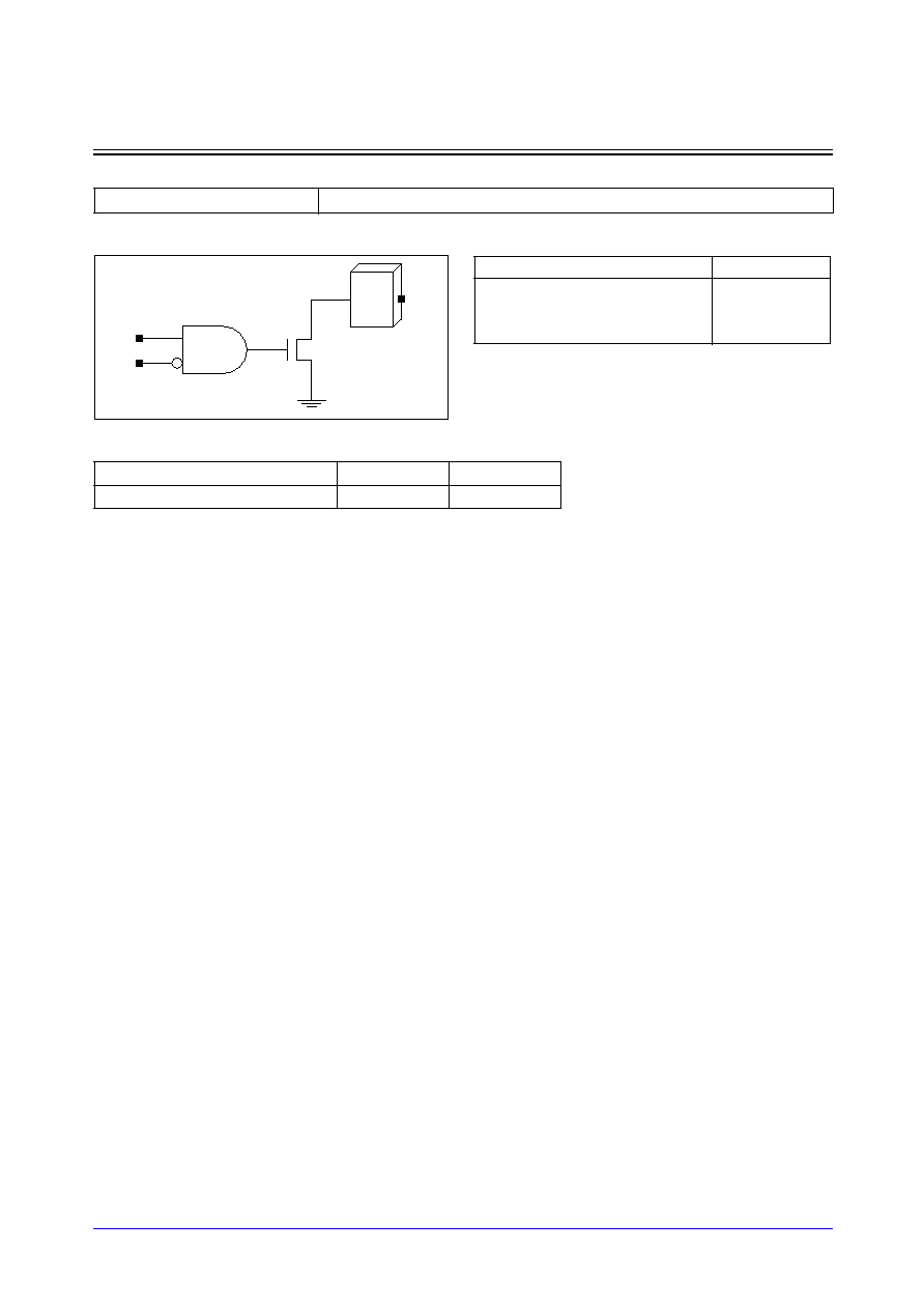
STDL130
4-166
Samsung ASIC
PvODyz_ABB_LP
Analog Open Drain Output Buffers with Separate Bulk-Bias
Cell Availability
Logic Symbol
Standard Load (SL)
3.3V Interface
PHOD4SM_ABB_LP
Cell Name
TN
EN
PHOD4SM_ABB_LP
2.47
2.97
Truth Table
TN
EN
PAD
1
0
0
0
x
Hi-Z
x
1
Hi-Z
PAD
TN
EN
Samsung ASIC
4-167
STDL130
PvODyz_ABB_LP
Analog Open Drain Output Buffers with Separate Bulk-Bias
Switching Characteristics
(Typical process, 25
∞
C, 3.3V, t
R
/t
F
= 0.20ns, CL: Capacitive Load[pF])
PHOD4SM_ABB_LP
Path
Parameter
Delay [ns]
CL = 50.0pF
Delay Equations [ns]
Group1*
Group2*
Group3*
TN to PAD
tF
8.628
0.565 + 0.161*CL
0.537 + 0.162*CL
0.514 + 0.162*CL
tPHL
5.367
1.053 + 0.086*CL
1.061 + 0.086*CL
1.062 + 0.086*CL
tPLZ
0.407
0.407 + 0.000*CL
0.407 + 0.000*CL
0.407 + 0.000*CL
EN to PAD
tF
8.628
0.565 + 0.161*CL
0.537 + 0.162*CL
0.514 + 0.162*CL
tPHL
5.430
1.116 + 0.086*CL
1.124 + 0.086*CL
1.125 + 0.086*CL
tPLZ
0.431
0.431 + 0.000*CL
0.431 + 0.000*CL
0.431 + 0.000*CL
*Group1 : CL < 50, *Group2 : 50 CL
<
<
=
= 75, *Group3 : 75 < CL
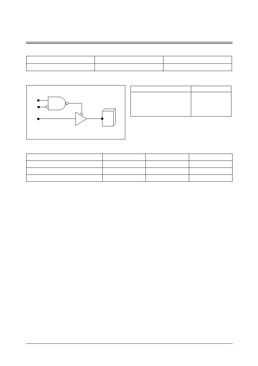
STDL130
4-168
Samsung ASIC
PvOTyz_ABB_LP
Analog Tri-state Output Buffers with Separate Bulk-Bias
Cell Availability
Logic Symbol
Standard Load (SL)
1.8V Only
2.5V Interface
3.3V Interface
POT(1/2/4/6/8/10/12/16)_ABB_LP
PMOT(1/2/4/6/8/10/12/16)_ABB_LP
PHOT(1/2/4/6/8/10/12/16)_ABB_LP
Cell Name
TN
EN
A
POT(1/2/4/6/8/10/12/16)_ABB_LP
3.80
3.69
3.67
PMOT(1/2/4/6/8/10/12/16)_ABB_LP
2.14
2.80
2.74
PHOT(1/2/4/6/8/10/12/16)_ABB_LP
2.37
2.98
2.69
Truth Table
TN
EN
A
PAD
1
0
0
0
1
0
1
1
x
1
x
Hi - z
0
x
x
Hi - z
EN
PAD
A
TN
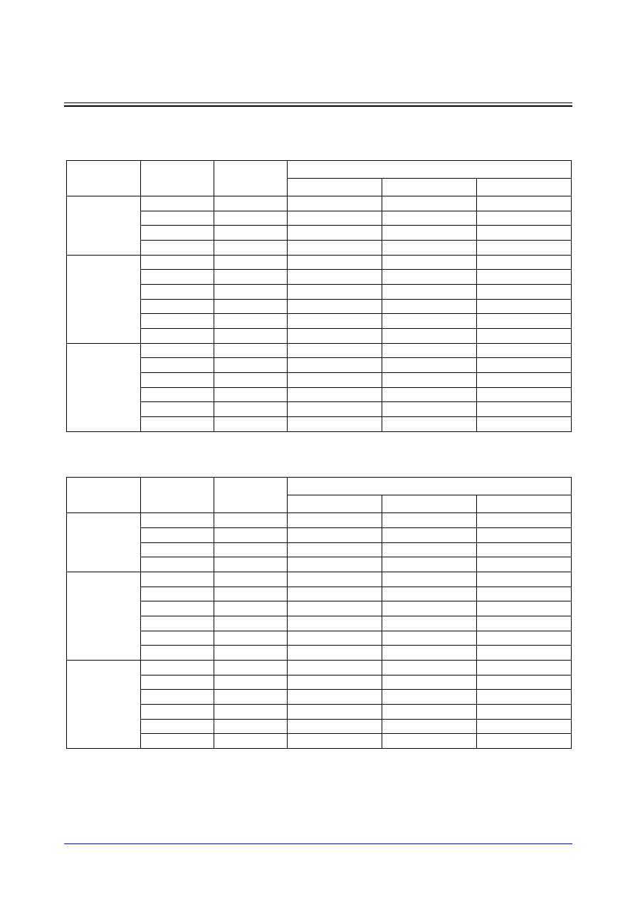
Samsung ASIC
4-169
STDL130
PvOTyz_ABB_LP
Analog Tri-state Output Buffers with Separate Bulk-Bias
Switching Characteristics
(Typical process, 25
∞
C, 1.8V, t
R
/t
F
= 0.20ns, CL: Capacitive Load[pF])
POT1_ABB_LP
POT2_ABB_LP
Path
Parameter
Delay [ns]
CL = 50.0pF
Delay Equations [ns]
Group1*
Group2*
Group3*
A to PAD
tR
20.215
1.333 + 0.378*CL
1.329 + 0.378*CL
1.326 + 0.378*CL
tF
22.775
1.555 + 0.424*CL
1.547 + 0.425*CL
1.541 + 0.425*CL
tPLH
9.897
0.983 + 0.178*CL
0.984 + 0.178*CL
0.983 + 0.178*CL
tPHL
12.442
1.575 + 0.217*CL
1.574 + 0.217*CL
1.577 + 0.217*CL
TN to PAD
tR
20.215
1.333 + 0.378*CL
1.329 + 0.378*CL
1.329 + 0.378*CL
tF
22.775
1.555 + 0.424*CL
1.547 + 0.425*CL
1.541 + 0.425*CL
tPLH
9.948
1.030 + 0.178*CL
1.032 + 0.178*CL
1.035 + 0.178*CL
tPHL
12.512
1.645 + 0.217*CL
1.644 + 0.217*CL
1.647 + 0.217*CL
tPLZ
0.670
0.670 + 0.000*CL
0.670 + 0.000*CL
0.670 + 0.000*CL
tPHZ
0.531
0.531 + 0.000*CL
0.531 + 0.000*CL
0.531 + 0.000*CL
EN to PAD
tR
20.215
1.333 + 0.378*CL
1.329 + 0.378*CL
1.329 + 0.378*CL
tF
22.775
1.555 + 0.424*CL
1.547 + 0.425*CL
1.541 + 0.425*CL
tPLH
10.013
1.096 + 0.178*CL
1.097 + 0.178*CL
1.097 + 0.178*CL
tPHL
12.578
1.710 + 0.217*CL
1.712 + 0.217*CL
1.709 + 0.217*CL
tPLZ
0.704
0.704 + 0.000*CL
0.704 + 0.000*CL
0.704 + 0.000*CL
tPHZ
0.565
0.565 + 0.000*CL
0.564 + 0.000*CL
0.565 + 0.000*CL
*Group1 : CL < 50, *Group2 : 50 CL
<
<
=
= 75, *Group3 : 75 < CL
Path
Parameter
Delay [ns]
CL = 50.0pF
Delay Equations [ns]
Group1*
Group2*
Group3*
A to PAD
tR
13.606
0.929 + 0.254*CL
0.928 + 0.254*CL
0.925 + 0.254*CL
tF
12.068
0.834 + 0.225*CL
0.830 + 0.225*CL
0.821 + 0.225*CL
tPLH
6.968
0.900 + 0.121*CL
0.901 + 0.121*CL
0.900 + 0.121*CL
tPHL
6.837
0.985 + 0.117*CL
0.985 + 0.117*CL
0.984 + 0.117*CL
TN to PAD
tR
13.606
0.929 + 0.254*CL
0.928 + 0.254*CL
0.925 + 0.254*CL
tF
12.068
0.834 + 0.225*CL
0.830 + 0.225*CL
0.821 + 0.225*CL
tPLH
7.019
0.948 + 0.121*CL
0.951 + 0.121*CL
0.951 + 0.121*CL
tPHL
6.906
1.053 + 0.117*CL
1.054 + 0.117*CL
1.054 + 0.117*CL
tPLZ
0.511
0.511 + 0.000*CL
0.511 + 0.000*CL
0.511 + 0.000*CL
tPHZ
0.824
0.824 + 0.000*CL
0.824 + 0.000*CL
0.824 + 0.000*CL
EN to PAD
tR
13.606
0.929 + 0.254*CL
0.928 + 0.254*CL
0.925 + 0.254*CL
tF
12.068
0.834 + 0.225*CL
0.830 + 0.225*CL
0.821 + 0.225*CL
tPLH
7.084
1.014 + 0.121*CL
1.017 + 0.121*CL
1.016 + 0.121*CL
tPHL
6.971
1.119 + 0.117*CL
1.120 + 0.117*CL
1.120 + 0.117*CL
tPLZ
0.545
0.545 + 0.000*CL
0.545 + 0.000*CL
0.545 + 0.000*CL
tPHZ
0.858
0.858 + 0.000*CL
0.858 + 0.000*CL
0.858 + 0.000*CL
*Group1 : CL < 50, *Group2 : 50 CL
<
<
=
= 75, *Group3 : 75 < CL

STDL130
4-170
Samsung ASIC
PvOTyz_ABB_LP
Analog Tri-state Output Buffers with Separate Bulk-Bias
Switching Characteristics
(Typical process, 25
∞
C, 1.8V, t
R
/t
F
= 0.20ns, CL: Capacitive Load[pF])
POT4_ABB_LP
POT6_ABB_LP
Path
Parameter
Delay [ns]
CL = 50.0pF
Delay Equations [ns]
Group1*
Group2*
Group3*
A to PAD
tR
6.780
0.488 + 0.126*CL
0.488 + 0.126*CL
0.485 + 0.126*CL
tF
6.826
0.493 + 0.127*CL
0.491 + 0.127*CL
0.487 + 0.127*CL
tPLH
3.655
0.680 + 0.059*CL
0.682 + 0.059*CL
0.683 + 0.059*CL
tPHL
4.103
0.688 + 0.068*CL
0.690 + 0.068*CL
0.690 + 0.068*CL
TN to PAD
tR
6.780
0.488 + 0.126*CL
0.488 + 0.126*CL
0.485 + 0.126*CL
tF
6.826
0.493 + 0.127*CL
0.491 + 0.127*CL
0.487 + 0.127*CL
tPLH
3.705
0.728 + 0.060*CL
0.732 + 0.059*CL
0.733 + 0.059*CL
tPHL
4.170
0.750 + 0.068*CL
0.755 + 0.068*CL
0.756 + 0.068*CL
tPLZ
0.428
0.428 + 0.000*CL
0.428 + 0.000*CL
0.428 + 0.000*CL
tPHZ
0.832
0.832 + 0.000*CL
0.832 + 0.000*CL
0.832 + 0.000*CL
EN to PAD
tR
6.780
0.488 + 0.126*CL
0.488 + 0.126*CL
0.485 + 0.126*CL
tF
6.826
0.493 + 0.127*CL
0.490 + 0.127*CL
0.487 + 0.127*CL
tPLH
3.770
0.794 + 0.060*CL
0.797 + 0.059*CL
0.799 + 0.059*CL
tPHL
4.235
0.816 + 0.068*CL
0.820 + 0.068*CL
0.822 + 0.068*CL
tPLZ
0.463
0.463 + 0.000*CL
0.463 + 0.000*CL
0.463 + 0.000*CL
tPHZ
0.866
0.866 + 0.000*CL
0.866 + 0.000*CL
0.866 + 0.000*CL
*Group1 : CL < 50, *Group2 : 50 CL
<
<
=
= 75, *Group3 : 75 < CL
Path
Parameter
Delay [ns]
CL = 50.0pF
Delay Equations [ns]
Group1*
Group2*
Group3*
A to PAD
tR
4.723
0.370 + 0.087*CL
0.361 + 0.087*CL
0.358 + 0.087*CL
tF
4.392
0.364 + 0.081*CL
0.351 + 0.081*CL
0.343 + 0.081*CL
tPLH
2.908
0.833 + 0.042*CL
0.837 + 0.041*CL
0.839 + 0.041*CL
tPHL
2.989
0.837 + 0.043*CL
0.836 + 0.043*CL
0.835 + 0.043*CL
TN to PAD
tR
4.723
0.370 + 0.087*CL
0.361 + 0.087*CL
0.358 + 0.087*CL
tF
4.391
0.359 + 0.081*CL
0.349 + 0.081*CL
0.342 + 0.081*CL
tPLH
2.959
0.882 + 0.042*CL
0.886 + 0.041*CL
0.889 + 0.041*CL
tPHL
3.045
0.875 + 0.043*CL
0.884 + 0.043*CL
0.889 + 0.043*CL
tPLZ
0.594
0.593 + 0.000*CL
0.593 + 0.000*CL
0.593 + 0.000*CL
tPHZ
1.411
1.411 + 0.000*CL
1.411 + 0.000*CL
1.411 + 0.000*CL
EN to PAD
tR
4.723
0.370 + 0.087*CL
0.361 + 0.087*CL
0.358 + 0.087*CL
tF
4.391
0.359 + 0.081*CL
0.349 + 0.081*CL
0.342 + 0.081*CL
tPLH
3.024
0.948 + 0.042*CL
0.952 + 0.041*CL
0.954 + 0.041*CL
tPHL
3.111
0.941 + 0.043*CL
0.950 + 0.043*CL
0.954 + 0.043*CL
tPLZ
0.627
0.627 + 0.000*CL
0.627 + 0.000*CL
0.627 + 0.000*CL
tPHZ
1.445
1.445 + 0.000*CL
1.445 + 0.000*CL
1.445 + 0.000*CL
*Group1 : CL < 50, *Group2 : 50 CL
<
<
=
= 75, *Group3 : 75 < CL

Samsung ASIC
4-171
STDL130
PvOTyz_ABB_LP
Analog Tri-state Output Buffers with Separate Bulk-Bias
Switching Characteristics
(Typical process, 25
∞
C, 1.8V, t
R
/t
F
= 0.20ns, CL: Capacitive Load[pF])
POT8_ABB_LP
POT10_ABB_LP
Path
Parameter
Delay [ns]
CL = 50.0pF
Delay Equations [ns]
Group1*
Group2*
Group3*
A to PAD
tR
3.401
0.255 + 0.063*CL
0.254 + 0.063*CL
0.254 + 0.063*CL
tF
3.423
0.256 + 0.063*CL
0.255 + 0.063*CL
0.254 + 0.063*CL
tPLH
2.115
0.627 + 0.030*CL
0.628 + 0.030*CL
0.629 + 0.030*CL
tPHL
2.289
0.583 + 0.034*CL
0.583 + 0.034*CL
0.583 + 0.034*CL
TN to PAD
tR
3.401
0.255 + 0.063*CL
0.254 + 0.063*CL
0.254 + 0.063*CL
tF
3.422
0.253 + 0.063*CL
0.253 + 0.063*CL
0.253 + 0.063*CL
tPLH
2.166
0.675 + 0.030*CL
0.678 + 0.030*CL
0.679 + 0.030*CL
tPHL
2.352
0.637 + 0.034*CL
0.641 + 0.034*CL
0.644 + 0.034*CL
tPLZ
0.460
0.460 + 0.000*CL
0.460 + 0.000*CL
0.460 + 0.000*CL
tPHZ
0.876
0.876 + 0.000*CL
0.876 + 0.000*CL
0.876 + 0.000*CL
EN to PAD
tR
3.401
0.255 + 0.063*CL
0.254 + 0.063*CL
0.254 + 0.063*CL
tF
3.423
0.253 + 0.063*CL
0.254 + 0.063*CL
0.253 + 0.063*CL
tPLH
2.231
0.741 + 0.030*CL
0.743 + 0.030*CL
0.745 + 0.030*CL
tPHL
2.417
0.702 + 0.034*CL
0.707 + 0.034*CL
0.710 + 0.034*CL
tPLZ
0.495
0.495 + 0.000*CL
0.495 + 0.000*CL
0.495 + 0.000*CL
tPHZ
0.910
0.910 + 0.000*CL
0.910 + 0.000*CL
0.910 + 0.000*CL
*Group1 : CL < 50, *Group2 : 50 CL
<
<
=
= 75, *Group3 : 75 < CL
Path
Parameter
Delay [ns]
CL = 50.0pF
Delay Equations [ns]
Group1*
Group2*
Group3*
A to PAD
tR
2.561
0.209 + 0.047*CL
0.203 + 0.047*CL
0.201 + 0.047*CL
tF
2.689
0.231 + 0.049*CL
0.222 + 0.049*CL
0.217 + 0.049*CL
tPLH
1.778
0.660 + 0.022*CL
0.662 + 0.022*CL
0.663 + 0.022*CL
tPHL
1.990
0.670 + 0.026*CL
0.669 + 0.026*CL
0.669 + 0.026*CL
TN to PAD
tR
2.561
0.209 + 0.047*CL
0.203 + 0.047*CL
0.200 + 0.047*CL
tF
2.688
0.227 + 0.049*CL
0.220 + 0.049*CL
0.216 + 0.049*CL
tPLH
1.829
0.709 + 0.022*CL
0.712 + 0.022*CL
0.714 + 0.022*CL
tPHL
2.051
0.719 + 0.027*CL
0.725 + 0.027*CL
0.728 + 0.026*CL
tPLZ
0.543
0.543 + 0.000*CL
0.543 + 0.000*CL
0.543 + 0.000*CL
tPHZ
1.023
1.023 + 0.000*CL
1.023 + 0.000*CL
1.023 + 0.000*CL
EN to PAD
tR
2.561
0.209 + 0.047*CL
0.203 + 0.047*CL
0.200 + 0.047*CL
tF
2.688
0.227 + 0.049*CL
0.220 + 0.049*CL
0.216 + 0.049*CL
tPLH
1.894
0.775 + 0.022*CL
0.777 + 0.022*CL
0.779 + 0.022*CL
tPHL
2.116
0.785 + 0.027*CL
0.790 + 0.027*CL
0.794 + 0.026*CL
tPLZ
0.577
0.577 + 0.000*CL
0.577 + 0.000*CL
0.577 + 0.000*CL
tPHZ
1.057
1.056 + 0.000*CL
1.057 + 0.000*CL
1.057 + 0.000*CL
*Group1 : CL < 50, *Group2 : 50 CL
<
<
=
= 75, *Group3 : 75 < CL

STDL130
4-172
Samsung ASIC
PvOTyz_ABB_LP
Analog Tri-state Output Buffers with Separate Bulk-Bias
Switching Characteristics
(Typical process, 25
∞
C, 1.8V, t
R
/t
F
= 0.20ns, CL: Capacitive Load[pF])
POT12_ABB_LP
POT16_ABB_LP
Path
Parameter
Delay [ns]
CL = 50.0pF
Delay Equations [ns]
Group1*
Group2*
Group3*
A to PAD
tR
2.287
0.203 + 0.042*CL
0.193 + 0.042*CL
0.188 + 0.042*CL
tF
2.301
0.211 + 0.042*CL
0.193 + 0.042*CL
0.188 + 0.042*CL
tPLH
1.675
0.681 + 0.020*CL
0.682 + 0.020*CL
0.684 + 0.020*CL
tPHL
1.748
0.621 + 0.023*CL
0.615 + 0.023*CL
0.612 + 0.023*CL
TN to PAD
tR
2.287
0.203 + 0.042*CL
0.193 + 0.042*CL
0.188 + 0.042*CL
tF
2.298
0.192 + 0.042*CL
0.187 + 0.042*CL
0.185 + 0.042*CL
tPLH
1.726
0.729 + 0.020*CL
0.732 + 0.020*CL
0.734 + 0.020*CL
tPHL
1.799
0.651 + 0.023*CL
0.655 + 0.023*CL
0.660 + 0.023*CL
tPLZ
0.503
0.503 + 0.000*CL
0.503 + 0.000*CL
0.503 + 0.000*CL
tPHZ
1.097
1.096 + 0.000*CL
1.096 + 0.000*CL
1.097 + 0.000*CL
EN to PAD
tR
2.287
0.203 + 0.042*CL
0.193 + 0.042*CL
0.188 + 0.042*CL
tF
2.298
0.192 + 0.042*CL
0.187 + 0.042*CL
0.185 + 0.042*CL
tPLH
1.791
0.795 + 0.020*CL
0.798 + 0.020*CL
0.799 + 0.020*CL
tPHL
1.864
0.716 + 0.023*CL
0.721 + 0.023*CL
0.725 + 0.023*CL
tPLZ
0.537
0.537 + 0.000*CL
0.537 + 0.000*CL
0.537 + 0.000*CL
tPHZ
1.131
1.130 + 0.000*CL
1.130 + 0.000*CL
1.131 + 0.000*CL
*Group1 : CL < 50, *Group2 : 50 CL
<
<
=
= 75, *Group3 : 75 < CL
Path
Parameter
Delay [ns]
CL = 50.0pF
Delay Equations [ns]
Group1*
Group2*
Group3*
A to PAD
tR
1.744
0.203 + 0.031*CL
0.185 + 0.031*CL
0.173 + 0.031*CL
tF
1.758
0.230 + 0.031*CL
0.199 + 0.031*CL
0.175 + 0.031*CL
tPLH
1.498
0.749 + 0.015*CL
0.752 + 0.015*CL
0.754 + 0.015*CL
tPHL
1.518
0.689 + 0.017*CL
0.678 + 0.017*CL
0.670 + 0.017*CL
TN to PAD
tR
1.744
0.203 + 0.031*CL
0.185 + 0.031*CL
0.172 + 0.031*CL
tF
1.744
0.179 + 0.031*CL
0.169 + 0.032*CL
0.161 + 0.032*CL
tPLH
1.549
0.798 + 0.015*CL
0.802 + 0.015*CL
0.804 + 0.015*CL
tPHL
1.551
0.686 + 0.017*CL
0.691 + 0.017*CL
0.695 + 0.017*CL
tPLZ
0.544
0.544 + 0.000*CL
0.544 + 0.000*CL
0.544 + 0.000*CL
tPHZ
1.316
1.316 + 0.000*CL
1.316 + 0.000*CL
1.316 + 0.000*CL
EN to PAD
tR
1.744
0.203 + 0.031*CL
0.185 + 0.031*CL
0.172 + 0.031*CL
tF
1.744
0.179 + 0.031*CL
0.169 + 0.032*CL
0.161 + 0.032*CL
tPLH
1.614
0.864 + 0.015*CL
0.868 + 0.015*CL
0.870 + 0.015*CL
tPHL
1.616
0.751 + 0.017*CL
0.756 + 0.017*CL
0.760 + 0.017*CL
tPLZ
0.578
0.578 + 0.000*CL
0.578 + 0.000*CL
0.578 + 0.000*CL
tPHZ
1.350
1.350 + 0.000*CL
1.350 + 0.000*CL
1.350 + 0.000*CL
*Group1 : CL < 50, *Group2 : 50 CL
<
<
=
= 75, *Group3 : 75 < CL
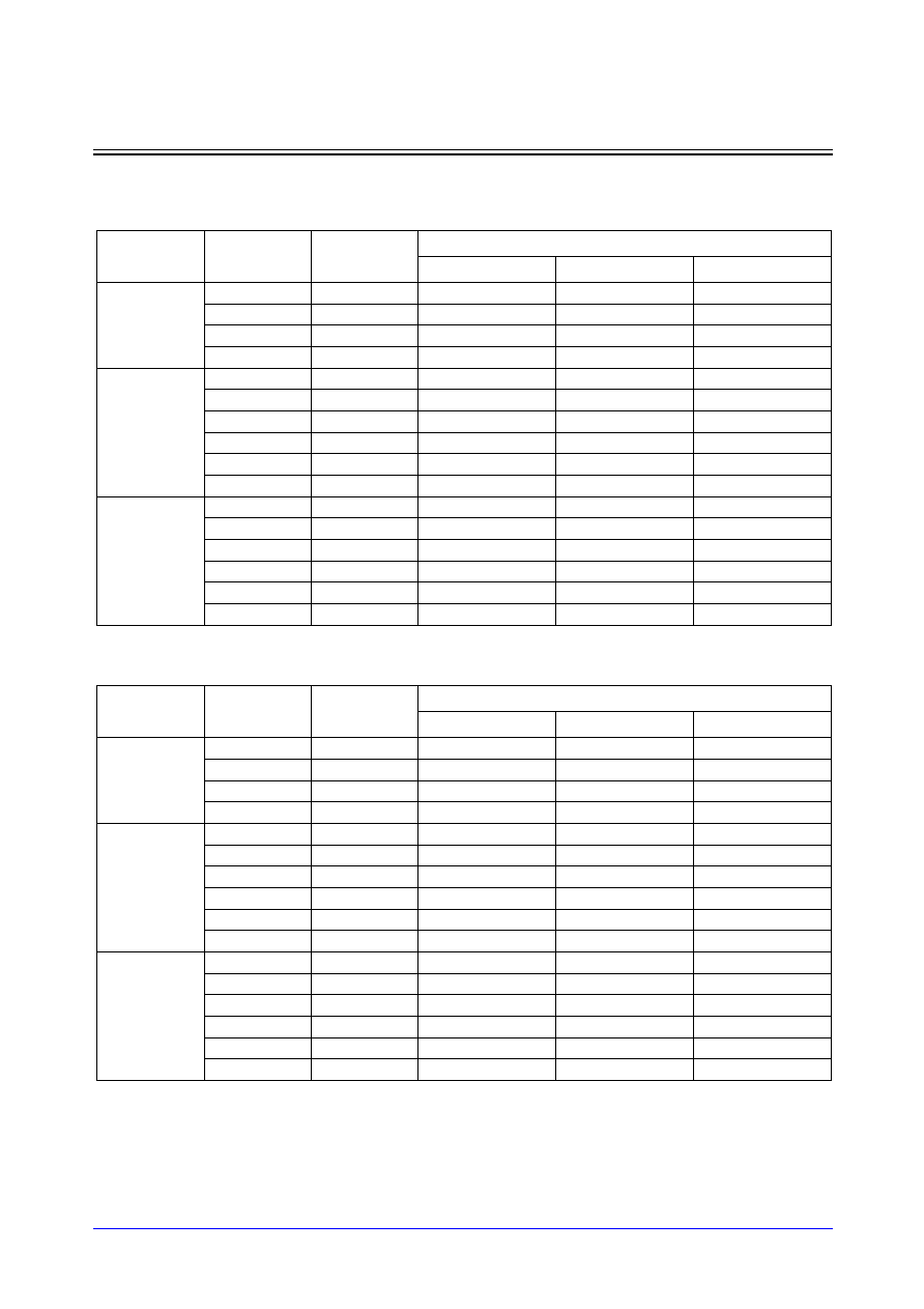
Samsung ASIC
4-173
STDL130
PvOTyz_ABB_LP
Analog Tri-state Output Buffers with Separate Bulk-Bias
Switching Characteristics
(Typical process, 25
∞
C, 2.5V, t
R
/t
F
= 0.20ns, CL: Capacitive Load[pF])
PMOT1_ABB_LP
PMOT2_ABB_LP
Path
Parameter
Delay [ns]
CL = 50.0pF
Delay Equations [ns]
Group1*
Group2*
Group3*
A to PAD
tR
25.865
1.230 + 0.493*CL
1.223 + 0.493*CL
1.223 + 0.493*CL
tF
22.620
1.062 + 0.431*CL
1.054 + 0.431*CL
1.051 + 0.431*CL
tPLH
12.996
1.125 + 0.237*CL
1.124 + 0.237*CL
1.124 + 0.237*CL
tPHL
12.272
1.135 + 0.223*CL
1.134 + 0.223*CL
1.134 + 0.223*CL
TN to PAD
tR
25.865
1.228 + 0.493*CL
1.223 + 0.493*CL
1.223 + 0.493*CL
tF
22.620
1.062 + 0.431*CL
1.054 + 0.431*CL
1.051 + 0.431*CL
tPLH
13.099
1.225 + 0.237*CL
1.227 + 0.237*CL
1.227 + 0.237*CL
tPHL
12.391
1.252 + 0.223*CL
1.253 + 0.223*CL
1.253 + 0.223*CL
tPLZ
0.757
0.757 + 0.000*CL
0.757 + 0.000*CL
0.757 + 0.000*CL
tPHZ
0.720
0.720 + 0.000*CL
0.720 + 0.000*CL
0.720 + 0.000*CL
EN to PAD
tR
25.865
1.228 + 0.493*CL
1.223 + 0.493*CL
1.223 + 0.493*CL
tF
22.620
1.062 + 0.431*CL
1.054 + 0.431*CL
1.051 + 0.431*CL
tPLH
13.168
1.295 + 0.237*CL
1.296 + 0.237*CL
1.296 + 0.237*CL
tPHL
12.460
1.321 + 0.223*CL
1.322 + 0.223*CL
1.322 + 0.223*CL
tPLZ
0.787
0.787 + 0.000*CL
0.787 + 0.000*CL
0.787 + 0.000*CL
tPHZ
0.749
0.749 + 0.000*CL
0.749 + 0.000*CL
0.749 + 0.000*CL
*Group1 : CL < 50, *Group2 : 50 CL
<
<
=
= 75, *Group3 : 75 < CL
Path
Parameter
Delay [ns]
CL = 50.0pF
Delay Equations [ns]
Group1*
Group2*
Group3*
A to PAD
tR
12.964
0.652 + 0.246*CL
0.648 + 0.246*CL
0.642 + 0.246*CL
tF
12.899
0.622 + 0.246*CL
0.615 + 0.246*CL
0.612 + 0.246*CL
tPLH
6.887
0.950 + 0.119*CL
0.951 + 0.119*CL
0.952 + 0.119*CL
tPHL
7.421
0.823 + 0.132*CL
0.822 + 0.132*CL
0.824 + 0.132*CL
TN to PAD
tR
12.964
0.652 + 0.246*CL
0.648 + 0.246*CL
0.642 + 0.246*CL
tF
12.899
0.622 + 0.246*CL
0.615 + 0.246*CL
0.612 + 0.246*CL
tPLH
6.989
1.050 + 0.119*CL
1.053 + 0.119*CL
1.054 + 0.119*CL
tPHL
7.538
0.937 + 0.132*CL
0.939 + 0.132*CL
0.938 + 0.132*CL
tPLZ
0.655
0.655 + 0.000*CL
0.655 + 0.000*CL
0.655 + 0.000*CL
tPHZ
0.872
0.872 + 0.000*CL
0.872 + 0.000*CL
0.872 + 0.000*CL
EN to PAD
tR
12.964
0.652 + 0.246*CL
0.648 + 0.246*CL
0.642 + 0.246*CL
tF
12.899
0.622 + 0.246*CL
0.615 + 0.246*CL
0.612 + 0.246*CL
tPLH
7.059
1.120 + 0.119*CL
1.122 + 0.119*CL
1.123 + 0.119*CL
tPHL
7.607
1.006 + 0.132*CL
1.008 + 0.132*CL
1.007 + 0.132*CL
tPLZ
0.685
0.685 + 0.000*CL
0.685 + 0.000*CL
0.685 + 0.000*CL
tPHZ
0.901
0.901 + 0.000*CL
0.901 + 0.000*CL
0.901 + 0.000*CL
*Group1 : CL < 50, *Group2 : 50 CL
<
<
=
= 75, *Group3 : 75 < CL

STDL130
4-174
Samsung ASIC
PvOTyz_ABB_LP
Analog Tri-state Output Buffers with Separate Bulk-Bias
Switching Characteristics
(Typical process, 25
∞
C, 2.5V, t
R
/t
F
= 0.20ns, CL: Capacitive Load[pF])
PMOT4_ABB_LP
PMOT6_ABB_LP
Path
Parameter
Delay [ns]
CL = 50.0pF
Delay Equations [ns]
Group1*
Group2*
Group3*
A to PAD
tR
6.523
0.379 + 0.123*CL
0.370 + 0.123*CL
0.366 + 0.123*CL
tF
6.472
0.340 + 0.123*CL
0.336 + 0.123*CL
0.332 + 0.123*CL
tPLH
3.983
1.008 + 0.059*CL
1.013 + 0.059*CL
1.015 + 0.059*CL
tPHL
4.037
0.746 + 0.066*CL
0.742 + 0.066*CL
0.739 + 0.066*CL
TN to PAD
tR
6.523
0.379 + 0.123*CL
0.370 + 0.123*CL
0.366 + 0.123*CL
tF
6.472
0.338 + 0.123*CL
0.336 + 0.123*CL
0.332 + 0.123*CL
tPLH
4.085
1.109 + 0.060*CL
1.114 + 0.059*CL
1.117 + 0.059*CL
tPHL
4.146
0.840 + 0.066*CL
0.845 + 0.066*CL
0.846 + 0.066*CL
tPLZ
0.760
0.760 + 0.000*CL
0.760 + 0.000*CL
0.760 + 0.000*CL
tPHZ
1.173
1.173 + 0.000*CL
1.173 + 0.000*CL
1.173 + 0.000*CL
EN to PAD
tR
6.523
0.378 + 0.123*CL
0.370 + 0.123*CL
0.366 + 0.123*CL
tF
6.472
0.338 + 0.123*CL
0.336 + 0.123*CL
0.332 + 0.123*CL
tPLH
4.154
1.179 + 0.060*CL
1.184 + 0.059*CL
1.186 + 0.059*CL
tPHL
4.215
0.909 + 0.066*CL
0.914 + 0.066*CL
0.915 + 0.066*CL
tPLZ
0.789
0.789 + 0.000*CL
0.789 + 0.000*CL
0.790 + 0.000*CL
tPHZ
1.201
1.201 + 0.000*CL
1.201 + 0.000*CL
1.201 + 0.000*CL
*Group1 : CL < 50, *Group2 : 50 CL
<
<
=
= 75, *Group3 : 75 < CL
Path
Parameter
Delay [ns]
CL = 50.0pF
Delay Equations [ns]
Group1*
Group2*
Group3*
A to PAD
tR
4.403
0.353 + 0.081*CL
0.320 + 0.082*CL
0.300 + 0.082*CL
tF
4.337
0.274 + 0.081*CL
0.251 + 0.082*CL
0.246 + 0.082*CL
tPLH
3.143
1.154 + 0.040*CL
1.160 + 0.040*CL
1.164 + 0.040*CL
tPHL
2.972
0.795 + 0.044*CL
0.785 + 0.044*CL
0.777 + 0.044*CL
TN to PAD
tR
4.403
0.352 + 0.081*CL
0.320 + 0.082*CL
0.300 + 0.082*CL
tF
4.336
0.253 + 0.082*CL
0.248 + 0.082*CL
0.245 + 0.082*CL
tPLH
3.246
1.255 + 0.040*CL
1.262 + 0.040*CL
1.266 + 0.040*CL
tPHL
3.062
0.850 + 0.044*CL
0.858 + 0.044*CL
0.862 + 0.044*CL
tPLZ
0.862
0.862 + 0.000*CL
0.862 + 0.000*CL
0.862 + 0.000*CL
tPHZ
1.470
1.470 + 0.000*CL
1.470 + 0.000*CL
1.470 + 0.000*CL
EN to PAD
tR
4.403
0.353 + 0.081*CL
0.320 + 0.082*CL
0.300 + 0.082*CL
tF
4.336
0.253 + 0.082*CL
0.248 + 0.082*CL
0.245 + 0.082*CL
tPLH
3.315
1.324 + 0.040*CL
1.332 + 0.040*CL
1.335 + 0.040*CL
tPHL
3.131
0.920 + 0.044*CL
0.927 + 0.044*CL
0.931 + 0.044*CL
tPLZ
0.891
0.891 + 0.000*CL
0.891 + 0.000*CL
0.891 + 0.000*CL
tPHZ
1.499
1.499 + 0.000*CL
1.499 + 0.000*CL
1.499 + 0.000*CL
*Group1 : CL < 50, *Group2 : 50 CL
<
<
=
= 75, *Group3 : 75 < CL
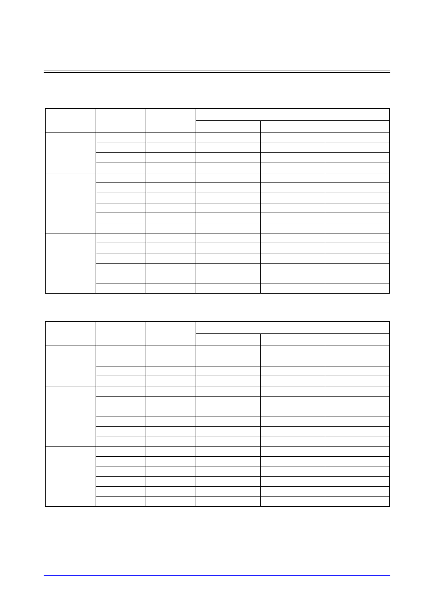
Samsung ASIC
4-175
STDL130
PvOTyz_ABB_LP
Analog Tri-state Output Buffers with Separate Bulk-Bias
Switching Characteristics
(Typical process, 25
∞
C, 2.5V, t
R
/t
F
= 0.20ns, CL: Capacitive Load[pF])
PMOT8_ABB_LP
PMOT10_ABB_LP
Path
Parameter
Delay [ns]
CL = 50.0pF
Delay Equations [ns]
Group1*
Group2*
Group3*
A to PAD
tR
3.383
0.406 + 0.060*CL
0.358 + 0.061*CL
0.320 + 0.061*CL
tF
3.292
0.308 + 0.060*CL
0.257 + 0.061*CL
0.219 + 0.061*CL
tPLH
2.819
1.314 + 0.030*CL
1.327 + 0.030*CL
1.334 + 0.030*CL
tPHL
2.494
0.889 + 0.032*CL
0.869 + 0.033*CL
0.855 + 0.033*CL
TN to PAD
tR
3.383
0.405 + 0.060*CL
0.358 + 0.061*CL
0.320 + 0.061*CL
tF
3.276
0.227 + 0.061*CL
0.215 + 0.061*CL
0.208 + 0.061*CL
tPLH
2.922
1.415 + 0.030*CL
1.430 + 0.030*CL
1.436 + 0.030*CL
tPHL
2.554
0.888 + 0.033*CL
0.897 + 0.033*CL
0.903 + 0.033*CL
tPLZ
0.963
0.963 + 0.000*CL
0.963 + 0.000*CL
0.963 + 0.000*CL
tPHZ
1.766
1.766 + 0.000*CL
1.766 + 0.000*CL
1.766 + 0.000*CL
EN to PAD
tR
3.383
0.405 + 0.060*CL
0.358 + 0.061*CL
0.320 + 0.061*CL
tF
3.276
0.227 + 0.061*CL
0.215 + 0.061*CL
0.208 + 0.061*CL
tPLH
2.991
1.485 + 0.030*CL
1.499 + 0.030*CL
1.505 + 0.030*CL
tPHL
2.623
0.957 + 0.033*CL
0.967 + 0.033*CL
0.973 + 0.033*CL
tPLZ
0.992
0.992 + 0.000*CL
0.992 + 0.000*CL
0.992 + 0.000*CL
tPHZ
1.795
1.795 + 0.000*CL
1.795 + 0.000*CL
1.795 + 0.000*CL
*Group1 : CL < 50, *Group2 : 50 CL
<
<
=
= 75, *Group3 : 75 < CL
Path
Parameter
Delay [ns]
CL = 50.0pF
Delay Equations [ns]
Group1*
Group2*
Group3*
A to PAD
tR
2.814
0.487 + 0.047*CL
0.434 + 0.048*CL
0.387 + 0.048*CL
tF
2.698
0.378 + 0.046*CL
0.314 + 0.048*CL
0.263 + 0.048*CL
tPLH
2.698
1.462 + 0.025*CL
1.496 + 0.024*CL
1.509 + 0.024*CL
tPHL
2.258
1.010 + 0.025*CL
0.978 + 0.026*CL
0.955 + 0.026*CL
TN to PAD
tR
2.814
0.486 + 0.047*CL
0.434 + 0.048*CL
0.387 + 0.048*CL
tF
2.649
0.228 + 0.048*CL
0.211 + 0.049*CL
0.199 + 0.049*CL
tPLH
2.801
1.564 + 0.025*CL
1.598 + 0.024*CL
1.612 + 0.024*CL
tPHL
2.276
0.936 + 0.027*CL
0.947 + 0.027*CL
0.954 + 0.026*CL
tPLZ
1.063
1.063 + 0.000*CL
1.063 + 0.000*CL
1.063 + 0.000*CL
tPHZ
2.061
2.060 + 0.000*CL
2.061 + 0.000*CL
2.061 + 0.000*CL
EN to PAD
tR
2.814
0.486 + 0.047*CL
0.434 + 0.048*CL
0.387 + 0.048*CL
tF
2.649
0.228 + 0.048*CL
0.211 + 0.049*CL
0.199 + 0.049*CL
tPLH
2.870
1.634 + 0.025*CL
1.667 + 0.024*CL
1.681 + 0.024*CL
tPHL
2.345
1.005 + 0.027*CL
1.016 + 0.027*CL
1.024 + 0.026*CL
tPLZ
1.093
1.093 + 0.000*CL
1.093 + 0.000*CL
1.093 + 0.000*CL
tPHZ
2.089
2.089 + 0.000*CL
2.089 + 0.000*CL
2.089 + 0.000*CL
*Group1 : CL < 50, *Group2 : 50 CL
<
<
=
= 75, *Group3 : 75 < CL

STDL130
4-176
Samsung ASIC
PvOTyz_ABB_LP
Analog Tri-state Output Buffers with Separate Bulk-Bias
Switching Characteristics
(Typical process, 25
∞
C, 2.5V, t
R
/t
F
= 0.20ns, CL: Capacitive Load[pF])
PMOT12_ABB_LP
PMOT16_ABB_LP
Path
Parameter
Delay [ns]
CL = 50.0pF
Delay Equations [ns]
Group1*
Group2*
Group3*
A to PAD
tR
2.276
0.303 + 0.039*CL
0.266 + 0.040*CL
0.237 + 0.041*CL
tF
2.265
0.348 + 0.038*CL
0.288 + 0.040*CL
0.241 + 0.040*CL
tPLH
2.180
1.174 + 0.020*CL
1.185 + 0.020*CL
1.189 + 0.020*CL
tPHL
2.051
1.022 + 0.021*CL
0.990 + 0.021*CL
0.968 + 0.022*CL
TN to PAD
tR
2.275
0.303 + 0.039*CL
0.266 + 0.040*CL
0.237 + 0.041*CL
tF
2.213
0.200 + 0.040*CL
0.183 + 0.041*CL
0.171 + 0.041*CL
tPLH
2.283
1.275 + 0.020*CL
1.288 + 0.020*CL
1.292 + 0.020*CL
tPHL
2.071
0.953 + 0.022*CL
0.962 + 0.022*CL
0.968 + 0.022*CL
tPLZ
0.912
0.912 + 0.000*CL
0.912 + 0.000*CL
0.912 + 0.000*CL
tPHZ
1.989
1.989 + 0.000*CL
1.989 + 0.000*CL
1.989 + 0.000*CL
EN to PAD
tR
2.275
0.303 + 0.039*CL
0.266 + 0.040*CL
0.237 + 0.041*CL
tF
2.213
0.200 + 0.040*CL
0.183 + 0.041*CL
0.171 + 0.041*CL
tPLH
2.352
1.345 + 0.020*CL
1.357 + 0.020*CL
1.361 + 0.020*CL
tPHL
2.140
1.023 + 0.022*CL
1.032 + 0.022*CL
1.037 + 0.022*CL
tPLZ
0.941
0.941 + 0.000*CL
0.941 + 0.000*CL
0.941 + 0.000*CL
tPHZ
2.018
2.017 + 0.000*CL
2.018 + 0.000*CL
2.018 + 0.000*CL
*Group1 : CL < 50, *Group2 : 50 CL
<
<
=
= 75, *Group3 : 75 < CL
Path
Parameter
Delay [ns]
CL = 50.0pF
Delay Equations [ns]
Group1*
Group2*
Group3*
A to PAD
tR
1.820
0.389 + 0.029*CL
0.352 + 0.029*CL
0.316 + 0.030*CL
tF
1.843
0.514 + 0.027*CL
0.424 + 0.028*CL
0.361 + 0.029*CL
tPLH
2.109
1.314 + 0.016*CL
1.350 + 0.015*CL
1.366 + 0.015*CL
tPHL
1.950
1.193 + 0.015*CL
1.190 + 0.015*CL
1.156 + 0.016*CL
TN to PAD
tR
1.820
0.388 + 0.029*CL
0.351 + 0.029*CL
0.315 + 0.030*CL
tF
1.714
0.231 + 0.030*CL
0.211 + 0.030*CL
0.192 + 0.030*CL
tPLH
2.212
1.416 + 0.016*CL
1.453 + 0.015*CL
1.469 + 0.015*CL
tPHL
1.884
1.030 + 0.017*CL
1.046 + 0.017*CL
1.055 + 0.017*CL
tPLZ
1.012
1.012 + 0.000*CL
1.012 + 0.000*CL
1.012 + 0.000*CL
tPHZ
2.428
2.428 + 0.000*CL
2.428 + 0.000*CL
2.428 + 0.000*CL
EN to PAD
tR
1.820
0.387 + 0.029*CL
0.351 + 0.029*CL
0.315 + 0.030*CL
tF
1.714
0.231 + 0.030*CL
0.211 + 0.030*CL
0.193 + 0.030*CL
tPLH
2.281
1.486 + 0.016*CL
1.522 + 0.015*CL
1.538 + 0.015*CL
tPHL
1.953
1.099 + 0.017*CL
1.116 + 0.017*CL
1.124 + 0.017*CL
tPLZ
1.042
1.041 + 0.000*CL
1.042 + 0.000*CL
1.042 + 0.000*CL
tPHZ
2.457
2.456 + 0.000*CL
2.457 + 0.000*CL
2.457 + 0.000*CL
*Group1 : CL < 50, *Group2 : 50 CL
<
<
=
= 75, *Group3 : 75 < CL

Samsung ASIC
4-177
STDL130
PvOTyz_ABB_LP
Analog Tri-state Output Buffers with Separate Bulk-Bias
Switching Characteristics
(Typical process, 25
∞
C, 3.3V, t
R
/t
F
= 0.20ns, CL: Capacitive Load[pF])
PHOT1_ABB_LP
PHOT2_ABB_LP
Path
Parameter
Delay [ns]
CL = 50.0pF
Delay Equations [ns]
Group1*
Group2*
Group3*
A to PAD
tR
35.745
1.770 + 0.679*CL
1.769 + 0.680*CL
1.769 + 0.680*CL
tF
26.361
1.304 + 0.501*CL
1.299 + 0.501*CL
1.296 + 0.501*CL
tPLH
17.279
1.314 + 0.319*CL
1.313 + 0.319*CL
1.313 + 0.319*CL
tPHL
13.222
1.271 + 0.239*CL
1.272 + 0.239*CL
1.272 + 0.239*CL
TN to PAD
tR
35.744
1.772 + 0.679*CL
1.768 + 0.680*CL
1.768 + 0.680*CL
tF
26.360
1.303 + 0.501*CL
1.298 + 0.501*CL
1.295 + 0.501*CL
tPLH
17.349
1.379 + 0.319*CL
1.383 + 0.319*CL
1.383 + 0.319*CL
tPHL
13.305
1.355 + 0.239*CL
1.353 + 0.239*CL
1.356 + 0.239*CL
tPLZ
0.845
0.845 + 0.000*CL
0.845 + 0.000*CL
0.845 + 0.000*CL
tPHZ
0.677
0.677 + 0.000*CL
0.677 + 0.000*CL
0.677 + 0.000*CL
EN to PAD
tR
35.744
1.772 + 0.679*CL
1.768 + 0.680*CL
1.768 + 0.680*CL
tF
26.360
1.303 + 0.501*CL
1.298 + 0.501*CL
1.295 + 0.501*CL
tPLH
17.412
1.445 + 0.319*CL
1.444 + 0.319*CL
1.447 + 0.319*CL
tPHL
13.369
1.417 + 0.239*CL
1.419 + 0.239*CL
1.419 + 0.239*CL
tPLZ
0.868
0.868 + 0.000*CL
0.868 + 0.000*CL
0.868 + 0.000*CL
tPHZ
0.700
0.700 + 0.000*CL
0.700 + 0.000*CL
0.700 + 0.000*CL
*Group1 : CL < 50, *Group2 : 50 CL
<
<
=
= 75, *Group3 : 75 < CL
Path
Parameter
Delay [ns]
CL = 50.0pF
Delay Equations [ns]
Group1*
Group2*
Group3*
A to PAD
tR
18.489
0.954 + 0.351*CL
0.951 + 0.351*CL
0.948 + 0.351*CL
tF
14.517
0.744 + 0.275*CL
0.739 + 0.276*CL
0.736 + 0.276*CL
tPLH
9.101
0.816 + 0.166*CL
0.816 + 0.166*CL
0.815 + 0.166*CL
tPHL
7.723
0.863 + 0.137*CL
0.864 + 0.137*CL
0.860 + 0.137*CL
TN to PAD
tR
18.489
0.954 + 0.351*CL
0.951 + 0.351*CL
0.948 + 0.351*CL
tF
14.517
0.744 + 0.275*CL
0.739 + 0.276*CL
0.736 + 0.276*CL
tPLH
9.170
0.883 + 0.166*CL
0.884 + 0.166*CL
0.884 + 0.166*CL
tPHL
7.806
0.945 + 0.137*CL
0.945 + 0.137*CL
0.947 + 0.137*CL
tPLZ
0.641
0.641 + 0.000*CL
0.641 + 0.000*CL
0.641 + 0.000*CL
tPHZ
0.550
0.550 + 0.000*CL
0.550 + 0.000*CL
0.550 + 0.000*CL
EN to PAD
tR
18.489
0.954 + 0.351*CL
0.951 + 0.351*CL
0.948 + 0.351*CL
tF
14.517
0.743 + 0.275*CL
0.739 + 0.276*CL
0.736 + 0.276*CL
tPLH
9.234
0.947 + 0.166*CL
0.947 + 0.166*CL
0.948 + 0.166*CL
tPHL
7.870
1.009 + 0.137*CL
1.009 + 0.137*CL
1.010 + 0.137*CL
tPLZ
0.664
0.664 + 0.000*CL
0.664 + 0.000*CL
0.664 + 0.000*CL
tPHZ
0.574
0.574 + 0.000*CL
0.574 + 0.000*CL
0.574 + 0.000*CL
*Group1 : CL < 50, *Group2 : 50 CL
<
<
=
= 75, *Group3 : 75 < CL
STDL130
4-178
Samsung ASIC
PvOTyz_ABB_LP
Analog Tri-state Output Buffers with Separate Bulk-Bias
Switching Characteristics
(Typical process, 25
∞
C, 3.3V, t
R
/t
F
= 0.20ns, CL: Capacitive Load[pF])
PHOT4_ABB_LP
PHOT6_ABB_LP
Path
Parameter
Delay [ns]
CL = 50.0pF
Delay Equations [ns]
Group1*
Group2*
Group3*
A to PAD
tR
9.272
0.507 + 0.175*CL
0.505 + 0.175*CL
0.506 + 0.175*CL
tF
8.568
0.449 + 0.162*CL
0.447 + 0.162*CL
0.442 + 0.162*CL
tPLH
4.831
0.686 + 0.083*CL
0.688 + 0.083*CL
0.688 + 0.083*CL
tPHL
4.961
0.655 + 0.086*CL
0.655 + 0.086*CL
0.655 + 0.086*CL
TN to PAD
tR
9.272
0.507 + 0.175*CL
0.505 + 0.175*CL
0.506 + 0.175*CL
tF
8.568
0.449 + 0.162*CL
0.447 + 0.162*CL
0.442 + 0.162*CL
tPLH
4.901
0.754 + 0.083*CL
0.757 + 0.083*CL
0.758 + 0.083*CL
tPHL
5.043
0.735 + 0.086*CL
0.737 + 0.086*CL
0.737 + 0.086*CL
tPLZ
0.536
0.536 + 0.000*CL
0.536 + 0.000*CL
0.536 + 0.000*CL
tPHZ
0.681
0.681 + 0.000*CL
0.681 + 0.000*CL
0.681 + 0.000*CL
EN to PAD
tR
9.272
0.507 + 0.175*CL
0.505 + 0.175*CL
0.506 + 0.175*CL
tF
8.568
0.449 + 0.162*CL
0.447 + 0.162*CL
0.442 + 0.162*CL
tPLH
4.965
0.818 + 0.083*CL
0.821 + 0.083*CL
0.822 + 0.083*CL
tPHL
5.106
0.799 + 0.086*CL
0.800 + 0.086*CL
0.800 + 0.086*CL
tPLZ
0.560
0.560 + 0.000*CL
0.560 + 0.000*CL
0.560 + 0.000*CL
tPHZ
0.704
0.704 + 0.000*CL
0.704 + 0.000*CL
0.704 + 0.000*CL
*Group1 : CL < 50, *Group2 : 50 CL
<
<
=
= 75, *Group3 : 75 < CL
Path
Parameter
Delay [ns]
CL = 50.0pF
Delay Equations [ns]
Group1*
Group2*
Group3*
A to PAD
tR
6.196
0.356 + 0.117*CL
0.354 + 0.117*CL
0.351 + 0.117*CL
tF
5.401
0.302 + 0.102*CL
0.300 + 0.102*CL
0.296 + 0.102*CL
tPLH
3.469
0.704 + 0.055*CL
0.706 + 0.055*CL
0.707 + 0.055*CL
tPHL
3.334
0.685 + 0.053*CL
0.688 + 0.053*CL
0.689 + 0.053*CL
TN to PAD
tR
6.196
0.357 + 0.117*CL
0.354 + 0.117*CL
0.351 + 0.117*CL
tF
5.401
0.303 + 0.102*CL
0.300 + 0.102*CL
0.296 + 0.102*CL
tPLH
3.538
0.770 + 0.055*CL
0.774 + 0.055*CL
0.775 + 0.055*CL
tPHL
3.415
0.765 + 0.053*CL
0.768 + 0.053*CL
0.770 + 0.053*CL
tPLZ
0.745
0.745 + 0.000*CL
0.745 + 0.000*CL
0.745 + 0.000*CL
tPHZ
0.810
0.810 + 0.000*CL
0.810 + 0.000*CL
0.810 + 0.000*CL
EN to PAD
tR
6.196
0.357 + 0.117*CL
0.354 + 0.117*CL
0.351 + 0.117*CL
tF
5.401
0.302 + 0.102*CL
0.300 + 0.102*CL
0.296 + 0.102*CL
tPLH
3.602
0.833 + 0.055*CL
0.837 + 0.055*CL
0.839 + 0.055*CL
tPHL
3.478
0.828 + 0.053*CL
0.832 + 0.053*CL
0.833 + 0.053*CL
tPLZ
0.769
0.769 + 0.000*CL
0.769 + 0.000*CL
0.769 + 0.000*CL
tPHZ
0.833
0.833 + 0.000*CL
0.833 + 0.000*CL
0.833 + 0.000*CL
*Group1 : CL < 50, *Group2 : 50 CL
<
<
=
= 75, *Group3 : 75 < CL
Samsung ASIC
4-179
STDL130
PvOTyz_ABB_LP
Analog Tri-state Output Buffers with Separate Bulk-Bias
Switching Characteristics
(Typical process, 25
∞
C, 3.3V, t
R
/t
F
= 0.20ns, CL: Capacitive Load[pF])
PHOT8_ABB_LP
PHOT10_ABB_LP
Path
Parameter
Delay [ns]
CL = 50.0pF
Delay Equations [ns]
Group1*
Group2*
Group3*
A to PAD
tR
4.671
0.305 + 0.087*CL
0.293 + 0.088*CL
0.288 + 0.088*CL
tF
4.301
0.245 + 0.081*CL
0.243 + 0.081*CL
0.241 + 0.081*CL
tPLH
2.827
0.749 + 0.042*CL
0.753 + 0.041*CL
0.755 + 0.041*CL
tPHL
2.760
0.610 + 0.043*CL
0.610 + 0.043*CL
0.608 + 0.043*CL
TN to PAD
tR
4.671
0.305 + 0.087*CL
0.293 + 0.088*CL
0.288 + 0.088*CL
tF
4.301
0.243 + 0.081*CL
0.243 + 0.081*CL
0.241 + 0.081*CL
tPLH
2.897
0.817 + 0.042*CL
0.822 + 0.041*CL
0.825 + 0.041*CL
tPHL
2.834
0.675 + 0.043*CL
0.679 + 0.043*CL
0.682 + 0.043*CL
tPLZ
0.643
0.643 + 0.000*CL
0.643 + 0.000*CL
0.643 + 0.000*CL
tPHZ
0.940
0.940 + 0.000*CL
0.940 + 0.000*CL
0.940 + 0.000*CL
EN to PAD
tR
4.671
0.305 + 0.087*CL
0.293 + 0.088*CL
0.288 + 0.088*CL
tF
4.301
0.243 + 0.081*CL
0.243 + 0.081*CL
0.241 + 0.081*CL
tPLH
2.960
0.881 + 0.042*CL
0.886 + 0.041*CL
0.889 + 0.041*CL
tPHL
2.898
0.738 + 0.043*CL
0.742 + 0.043*CL
0.745 + 0.043*CL
tPLZ
0.666
0.666 + 0.000*CL
0.666 + 0.000*CL
0.666 + 0.000*CL
tPHZ
0.963
0.963 + 0.000*CL
0.963 + 0.000*CL
0.963 + 0.000*CL
*Group1 : CL < 50, *Group2 : 50 CL
<
<
=
= 75, *Group3 : 75 < CL
Path
Parameter
Delay [ns]
CL = 50.0pF
Delay Equations [ns]
Group1*
Group2*
Group3*
A to PAD
tR
3.760
0.291 + 0.069*CL
0.268 + 0.070*CL
0.254 + 0.070*CL
tF
3.338
0.221 + 0.062*CL
0.211 + 0.063*CL
0.205 + 0.063*CL
tPLH
2.479
0.816 + 0.033*CL
0.819 + 0.033*CL
0.822 + 0.033*CL
tPHL
2.338
0.701 + 0.033*CL
0.701 + 0.033*CL
0.701 + 0.033*CL
TN to PAD
tR
3.760
0.292 + 0.069*CL
0.268 + 0.070*CL
0.255 + 0.070*CL
tF
3.338
0.220 + 0.062*CL
0.210 + 0.063*CL
0.205 + 0.063*CL
tPLH
2.547
0.880 + 0.033*CL
0.886 + 0.033*CL
0.889 + 0.033*CL
tPHL
2.412
0.763 + 0.033*CL
0.769 + 0.033*CL
0.772 + 0.033*CL
tPLZ
0.849
0.849 + 0.000*CL
0.849 + 0.000*CL
0.849 + 0.000*CL
tPHZ
1.069
1.069 + 0.000*CL
1.069 + 0.000*CL
1.069 + 0.000*CL
EN to PAD
tR
3.760
0.292 + 0.069*CL
0.268 + 0.070*CL
0.255 + 0.070*CL
tF
3.338
0.220 + 0.062*CL
0.210 + 0.063*CL
0.205 + 0.063*CL
tPLH
2.611
0.944 + 0.033*CL
0.949 + 0.033*CL
0.953 + 0.033*CL
tPHL
2.475
0.826 + 0.033*CL
0.832 + 0.033*CL
0.836 + 0.033*CL
tPLZ
0.873
0.873 + 0.000*CL
0.873 + 0.000*CL
0.873 + 0.000*CL
tPHZ
1.092
1.092 + 0.000*CL
1.092 + 0.000*CL
1.092 + 0.000*CL
*Group1 : CL < 50, *Group2 : 50 CL
<
<
=
= 75, *Group3 : 75 < CL

STDL130
4-180
Samsung ASIC
PvOTyz_ABB_LP
Analog Tri-state Output Buffers with Separate Bulk-Bias
Switching Characteristics
(Typical process, 25
∞
C, 3.3V, t
R
/t
F
=0.20ns, CL: Capacitive Load[pF])
PHOT12_ABB_LP
PHOT16_ABB_LP
Path
Parameter
Delay [ns]
CL = 50.0pF
Delay Equations [ns]
Group1*
Group2*
Group3*
A to PAD
tR
3.169
0.309 + 0.057*CL
0.276 + 0.058*CL
0.253 + 0.058*CL
tF
2.887
0.216 + 0.053*CL
0.189 + 0.054*CL
0.180 + 0.054*CL
tPLH
2.272
0.880 + 0.028*CL
0.886 + 0.028*CL
0.890 + 0.028*CL
tPHL
2.080
0.663 + 0.028*CL
0.655 + 0.029*CL
0.649 + 0.029*CL
TN to PAD
tR
3.169
0.309 + 0.057*CL
0.276 + 0.058*CL
0.253 + 0.058*CL
tF
2.884
0.188 + 0.054*CL
0.182 + 0.054*CL
0.178 + 0.054*CL
tPLH
2.341
0.949 + 0.028*CL
0.955 + 0.028*CL
0.959 + 0.028*CL
tPHL
2.138
0.691 + 0.029*CL
0.698 + 0.029*CL
0.701 + 0.029*CL
tPLZ
0.747
0.747 + 0.000*CL
0.747 + 0.000*CL
0.747 + 0.000*CL
tPHZ
1.198
1.198 + 0.000*CL
1.198 + 0.000*CL
1.198 + 0.000*CL
EN to PAD
tR
3.169
0.309 + 0.057*CL
0.276 + 0.058*CL
0.253 + 0.058*CL
tF
2.884
0.188 + 0.054*CL
0.182 + 0.054*CL
0.178 + 0.054*CL
tPLH
2.405
1.013 + 0.028*CL
1.019 + 0.028*CL
1.023 + 0.028*CL
tPHL
2.201
0.755 + 0.029*CL
0.761 + 0.029*CL
0.765 + 0.029*CL
tPLZ
0.771
0.771 + 0.000*CL
0.771 + 0.000*CL
0.771 + 0.000*CL
tPHZ
1.221
1.222 + 0.000*CL
1.221 + 0.000*CL
1.221 + 0.000*CL
*Group1 : CL < 50, *Group2 : 50 CL
<
<
=
= 75, *Group3 : 75 < CL
Path
Parameter
Delay [ns]
CL = 50.0pF
Delay Equations [ns]
Group1*
Group2*
Group3*
A to PAD
tR
2.368
0.214 + 0.043*CL
0.192 + 0.044*CL
0.177 + 0.044*CL
tF
2.178
0.193 + 0.040*CL
0.164 + 0.040*CL
0.146 + 0.041*CL
tPLH
1.749
0.709 + 0.021*CL
0.711 + 0.021*CL
0.713 + 0.021*CL
tPHL
1.755
0.699 + 0.021*CL
0.689 + 0.021*CL
0.683 + 0.021*CL
TN to PAD
tR
2.368
0.214 + 0.043*CL
0.192 + 0.044*CL
0.178 + 0.044*CL
tF
2.172
0.157 + 0.040*CL
0.147 + 0.040*CL
0.142 + 0.041*CL
tPLH
1.820
0.778 + 0.021*CL
0.781 + 0.021*CL
0.784 + 0.021*CL
tPHL
1.808
0.722 + 0.022*CL
0.727 + 0.022*CL
0.731 + 0.022*CL
tPLZ
0.673
0.673 + 0.000*CL
0.673 + 0.000*CL
0.673 + 0.000*CL
tPHZ
1.230
1.231 + 0.000*CL
1.230 + 0.000*CL
1.230 + 0.000*CL
EN to PAD
tR
2.368
0.214 + 0.043*CL
0.192 + 0.044*CL
0.178 + 0.044*CL
tF
2.172
0.157 + 0.040*CL
0.147 + 0.040*CL
0.142 + 0.041*CL
tPLH
1.884
0.842 + 0.021*CL
0.846 + 0.021*CL
0.847 + 0.021*CL
tPHL
1.872
0.786 + 0.022*CL
0.791 + 0.022*CL
0.794 + 0.022*CL
tPLZ
0.697
0.697 + 0.000*CL
0.697 + 0.000*CL
0.697 + 0.000*CL
tPHZ
1.254
1.254 + 0.000*CL
1.254 + 0.000*CL
1.254 + 0.000*CL
*Group1 : CL < 50, *Group2 : 50 CL
<
<
=
= 75, *Group3 : 75 < CL
Samsung ASIC
4-181
STDL130
ESD Slot Cells
Cell List
Cell Name
Function Description
EV1I_LP
1.8V Internal ESD Protection
EV1P_LP
1.8V Pre-Driver ESD Protection
EV1O_LP
1.8V Output-Driver ESD Protection
EV1OP_LP
1.8V Output-Drive and Pre-Driver ESD Protection
EV1OP_ABB_LP
1.8V Output-Drive and Pre-Driver ESD Protection with Separate Bulk-Bias
EV1T_ABB_LP
1.8V Total ESD Protection with Separate Bulk-Bias
EV1IM_LP
1.8V Internal for 2.5V Interface ESD Protection
EV2P_LP
2.5V Pre-Driver ESD Protection
EV2O_LP
2.5V Output-Driver ESD Protection
EV2OP_LP
2.5V Output-Driver and Pre-Driver ESD Protection
EV2OP_ABB_LP
2.5V Output-Driver and Pre-Driver ESD Protection with Separate Bulk-Bias
EV2T_ABB_LP
2.5V Total ESD Protection with Separate Bulk-Bias
EV1IH_LP
1.8V Internal for 3.3V Interface ESD Protection
EV3P_LP
3.3V Pre-Driver ESD Protection
EV3O_LP
3.3V Output-Driver ESD Protection
EV3OP_LP
3.3V Output-Driver and Pre-Driver ESD Protection
EV3OP_ABB_LP
3.3V Output-Driver and Pre-Driver ESD Protection with Separate Bulk-Bias
EV3T_ABB_LP
3.3V Total ESD Protection with Separate Bulk-Bias
STDL130
4-182
Samsung ASIC
Common Slot Cells
Cell List
Cell Name
Function Description
EC0C0_LP
Metal Ring Separator between Different Digital Blocks
EC0C0D_LP
Metal Ring Separator between Different Digital Blocks for Noise Critical Design
EC0CA0_LP
Metal Ring Separator between Digital to Analog
EC0CA0D_LP
Metal Ring Separator between Digital to Analog for Noise Critical Design
ECA0CA0_LP
Metal Ring Separator between Different to Analog Blocks
ECA0CA0D_LP
Metal Ring Separator between Different to Analog Blocks for Noise
Critical Design
ECA0CA0_VBB_LP
Metal Ring Separator between Different Analog Blocks with VBB Ring
Connected
ECA0CA0D_VBB_LP
Metal Ring Separator between Different Analog Blocks for Noise Critical Design
with VBB Ring Connected

5
Compiled Memory

Contents
Overview .............................................................................................................................. 5-1
Compiled Memory Naming Convention................................................................................ 5-1
Characteristics for Timing and Power................................................................................... 5-2
Built-In Self Test and Built-In Redundancy-Analysis ............................................................ 5-4
Compiled Memory Selection Guide...................................................................................... 5-5
High-Density Compiled Memory
SPSRAM_HDL
High-Density Single-Port Synchronous SRAM ................................................... 5-9
SPSRAMBW_HDL High-Density Single-Port Synchronous SRAM with Bit-Write ............................. 5-24
SPSRAMR_HDL
High-Density Single-Port Synchronous SRAM with Redundancy....................... 5-39
DPSRAM_HDL
High-Density Dual-Port Synchronous SRAM ...................................................... 5-49
DPSRAMBW_HDL High-Density Dual-Port Synchronous SRAM with Bit-Write................................ 5-60
DROM_HDL
High-Density Synchronous Diffusion Programmable ROM................................. 5-71
MROM_HDL
High-Density Synchronous Metal-2 Programmable ROM................................... 5-83
ARFRAM_HDL
High-Density Multi-Port Asynchronous Register File .......................................... 5-95
FIFO_HDL
High-Density Synchronous First-In First-Out Memory ........................................ 5-115
CAM_HDL
High-Density Synchronous Content Addressable Memory................................. 5-127
Low-Power Compiled Memory
SPSRAM_LPL
Low-Power Single-Port Synchronous SRAM ...................................................... 5-141
SPSRAMBW_LPL
Low Power Single-Port Synchronous SRAM with Bit-Write ................................ 5-151
DPSRAM_LPL
Low-Power Dual-Port Synchronous SRAM......................................................... 5-162
DPSRAMBW_LPL
Low-Power Dual-Port Synchronous SRAM with Bit-Write................................... 5-173

COMPILED MEMORY
Overview
Samsung ASIC
5-1
STDL130
OVERVIEW
This section is an overview of the STDL130 compiled memory. In STDL130 compiled memories provide
application-specific memory solution high-density and low-power application. That is, two different compiled
memory libraries are available in STDL130:
STDL130-HD(High-Density) and STDL130-LP(Low-Power)
.
The high-density compiled memories are suitable for high integration application. The low-power compiled
memories are suitable for portable applications. Each of these memory types may be customized to satisfy
the specific circuit requirements. Each memory uses state-of-the-art design architecture techniques. The
final memory block is implemented as stand-alone, pitch-matched and customized leafcells. The compiled
memory is fully generated by a user-configurable compiler, called memory compiler.
The user defines the memory related specifications such as word depth, bit per word, and column mux type.
The compiler then produces any or all of the following items:
-- Complete functional model for simulation
-- Tabular model for timing and power characteristics
-- Automatic generated datasheet including all information for specific memory configuration
-- Full GDS and schematic netlist for layout verification
-- Phantom cell to use in chip-level floor planning and layout
Additional information about memory compilers can be obtained from your local Samsung Technology and
Design Centers.
COMPILED MEMORY NAMING CONVENTION
In this chapter, we describe the naming convention of memory. The memory name, Figure 5-1 consists of
the following convention.
Figure 5-1. Compiled Memory Naming Convention
The first string, `
memory_code
', means the name of memory type. In STDL130 compiled memory, the
available memory types are as follows:
∑
SPSRAM
: Single-Port Synchronous SRAM
∑
SPSRAMBW : Single-Port Synchronous SRAM with Bit-Write
∑ SPSRAMR
: Single-Port Synchronous SRAM with Redundancy
∑
DPSRAM
: Dual-Port Synchronous SRAM
∑ DPSRAMBW : Dual-Port Synchronous SRAM with Bit-Write
∑
DROM
: Synchronous Diffusion-Programmable ROM
∑
MROM
: Synchronous Metal2-Programmable ROM
∑ ARFRAM
: Multi-Port Asynchronous Register File
∑
FIFO
: Synchronous First-In First-Out Memory
∑ CAM
: Synchronous Content Addressable Memory
`memory_name':= [memory_code]_[appl_code]_[procs_code]_[opt_code]_[config_code]

Characteristics for Timing and Power
COMPILED MEMORY
STDL130
5-2
Samsung ASIC
The second string, '
appl_code
', means the specific application to suitably support the compiled memory and
the application code is one of HD(High-Density) and LP(Low-Power). The third string, '
procs_code
',
represents the process and the process code is one of Generic process and Low-Power process(L). In case
of Generic process, you don't have to specify '
procs_code
'. If there is no process code, it means that the
memory is developed under Generic process. If the process code is set to L, it means that the memory is
under Low-power process. The fourth string, '
opt_code
', represents the number of read and write ports for
multi-port memory and the option code is composed of the following convention:
`opt_code' = <n>r<m>w
Currently this field is only used for ARFRAM, where n is the total number of read ports (1~2) and m is the
total number of write ports (1~2). The last string, '
config_code
', represents the configuration of the memory
to be specified. This configuration code is composed of the following convention:
`config_code' = <WORD> x <BPW> m <YMUX> b <BANK>
Where, WORD is the word depth, BPW is bit per word, YMUX is the available column mux type and BANK
is the number of bank used. For example, 'spsram_hdl_1024x32m16b2' refers to a High-Density single-port
synchronous SRAM with 1024 words, 32 bits, 16 column mux and 2 bank under Generic process. Second,
'arfram_hdl_1r2w_32x32m2' refers to a High-Density three-port (1 read/2 write) asynchronous register file
with 32 word, 32 bits and 2 column mux under Generic process. 'spsram_lpl_1024x32m16' refers to a
Low-Power single-port synchronous SRAM with 1024 words, 32 bits 16 column mux under Low-power
process.
CHARACTERISTICS FOR TIMING AND POWER
STDL130 compiled memories are fully optimized for 1.8V
±
0.15V supply voltage. Compiled memory in this
section has been characterized using typical-process at 25 degree and 1.8V supply. The worst-case and
best-case parameters can be found by using the derating factor calculated from the following equation:
t
WC
(t
BC
) = K
P_local
◊
K
V_local
◊
K
T_local
◊
t
NOM
Where,
t
WC
is a worst-case propagation delay
t
BC
is a best-case propagation delay
t
NOM
is a typical-case propagation delay characterized under typical-process, 25 degree and 1.8V supply
K
P_local
is a local process derating factor corresponding to each memory type.
K
V_local
is a local voltage derating factor corresponding to each memory type.
K
T_local
is a local temperature derating factor that varies by memory type.
Note that
K
P_local
,
K
V_local
and
K
T_local
are only used in compiled memories.

COMPILED MEMORY
Characteristics for Timing and Power
Samsung ASIC
5-3
STDL130
A two-dimensional timing characteristics table look-up model has been adopted to yield more accuracy.
Based on the combination of input slopes and output loads, the propagation delay is measured from the
input crossing 50% V
DD
to the output crossing 50% V
DD
. The timing values reported in the tables are also
taken from the same voltage level as the switching characteristics with 0.2ns for input slope and 10SL
(Standard Load) for output load.
The power consumption for read and write modes is measured for on input slope of 0.2ns, an output load of
10SL and an input switching activity factor of 0.5. The total power consumption can be calculated by the
following equation:
P
total
= ((SA
read
◊
P
read
) + (SA
write
◊
P
write
))
◊
f
MAX
Where,
P
total
is the total power consumption in microwatts
P
read
is the read power consumption in microwatts per MHz
P
write
is the write power consumption in microwatts per MHz
SA
read
is the read access ratio on every cycle
SA
write
is the write access ratio on every cycle
f
MAX
is the RAM clock frequency in MHz.
The value of
SA
read
or
SA
write
is between 0 and 1. However, the sum of
SA
read
and
SA
write
must be less than
or equal to 1.
The power values reported in the tables are also taken from 50% switching activity, SA=0.5. For compiled
memory, the read power consumption, the write power consumption and the standby power consumption
are available. The standby power consumption is measured on the condition that CSN (Chip Select
Negative) disabled and for other signals in their normal operating mode except that OEN (Output Enable
Negative) is held low. If any of the signals are not active during standby mode, the standby power is near
zero and only static leakage power consumed. In dual-port memories, the power consumption is measured
with only one port active and the other port isolated.

Built-In Self Test and Built-in redundancy-analysis
COMPILED MEMORY
STDL130
5-4
Samsung ASIC
BUILT-IN SELF TEST AND BUILT-IN REDUNDANCY-ANALYSIS
Samsung provides engineering design services to support Built-In Self-Test (BIST) and Built-In
Redundancy Analysis (BIRA) for compiled memories.
BIST is the recommended test solution for compiled memories. Samsung BIST circuits are designed to
detect a complete range of fault types such as stuck-at faults, transition faults, coupling faults, and address
macrocells of the same or different types exist together in a circuit, Samsung supports the BIST for all to the
memories as a single architecture.
BIRA design services is also provided to test redundancy RAMs with testers. BIRA tests a SRAM and
generates fail information after redundancy analysis. The fail information gathered by logic tester is
automatically processed and transferred to the laser repair machine. For multiple redundancy RAMs,
Samsung BIRA architecture has an integration module to supp ort parallel testing, minimum test pin usage,
and optimize logic tester interface.
For more detailed information regarding to the BIST and BIRA, please contact your local Samsung
Technology and Design Centers.
COMPILED MEMORY
Selection Guide for Compiled Memory
Samsung ASIC
5-5
STDL130
SELECTION GUIDE FOR COMPILED MEMORY
High-Density Compiled Memory
High-Density
Description
SPSRAM_HDL
- High-Density Single-Port Synchronous Static RAM
- Duty-free clock operation
- Zero hold time for address, data-in and other control pins
- Dual bank available
- Flexible aspect ratio (Ymux = 4, 8, 16, 32)
SPSRAMBW_HDL
- High-Density Single-Port Synchronous Static RAM
- Bit-write feature available
- Duty-free clock operation
- Zero hold time for address, data-in and other control pins
- Dual bank available
- Flexible aspect ratio(Ymux = 4, 8, 16, 32)
SPSRAMR_HDL
- High-Density Single-Port Synchronous Static RAM with Redundancy
- Bit-write feature available
- Duty-free clock operation
- Zero hold time for address, data-in and other control pins
- Row-only redundancy available
- Failure analysis by BIRA and laser repair
- Flexible aspect ratio(Ymux = 8, 16, 32)
DPSRAM_HDL
- High-Density Dual-Port Synchronous Static RAM
- Duty-free clock operation
- Zero hold time for address, data-in and other control pins
- Flexible aspect ratio(Ymux = 4, 8, 16, 32)
DPSRAMBW_HDL
- High-Density Dual-Port Synchronous Static RAM
- Bit-write feature available
- Duty-free clock operation
- Zero hold time for address, data-in and other control pins
- Flexible aspect ratio(Ymux = 4, 8, 16, 32)
DROM_HDL
- High-Density Synchronous Diffusion programmable ROM
- Diffusion programmable coded
- Duty-free clock operation
- Zero hold time for address and other control pins
- Dual bank available
- Flexible aspect ratio(Ymux = 8, 16, 32)
MROM_HDL
- High-Density Synchronous Metal-2 programmable ROM
- Metal-2 programmable coded
- Duty-free clock operation
- Zero hold time for address and other control pins
- Dual bank available
- Flexible aspect ratio(Ymux = 8, 16, 32)
Selection Guide for Compiled Memory
COMPILED MEMORY
STDL130
5-6
Samsung ASIC
ARFRAM_HDL
- High-Density Multi-Port Asynchronous Register File
- Synchronous write operation / Asynchronous read operation
- 1-to-2 write ports / 1-to-2 read ports
- Flexible aspect ratio(Ymux = 2, 4, 8)
FIFO_HDL
- High-Density Synchronous First-In First-Out Memory
- Duty-free clock operation
- Reset and Re-transmit operation available
- Flexible aspect ratio(Ymux = 2, 4, 8, 16)
CAM_HDL
- High-Density Synchronous Binary Content Addressable Memory
- Duty-free clock operation
- Single cycle compare operation
- Built-in priority address encoder available
- Global hit/miss handling
High-Density
Description
COMPILED MEMORY
Selection Guide for Compiled Memory
Samsung ASIC
5-7
STDL130
Low-Power Compiled Memory
Low-Power
Description
SPSRAM_LPL
- Low-Power Single-Port Synchronous Static RAM
- Duty-free clock operation
- Zero hold time for address, data-in and other control pins
- Flexible aspect ratio(Ymux = 4, 8, 16, 32)
SPSRAMBW_LPL
- Low-Power Single-Port Synchronous Static RAM
- Bit-write feature available
- Duty-free clock operation
- Zero hold time for address, data-in and other control pins
- Flexible aspect ratio(Ymux = 4, 8, 16, 32)
DPSRAM_LPL
- Low-Power Dual-Port Synchronous Static RAM
- Duty-free clock operation
- Zero hold time for address, data-in and other control pins
- Flexible aspect ratio(Ymux = 2, 4, 8, 16)
DPSRAMBW_LPL
- Low-Power Dual-Port Synchronous Static RAM
- Bit-write feature available
- Duty-free clock operation
- Zero hold time for address, data-in and other control pins
- Flexible aspect ratio(Ymux = 2, 4, 8, 16)

STDL130
5-8
Samsung ASIC
NOTE
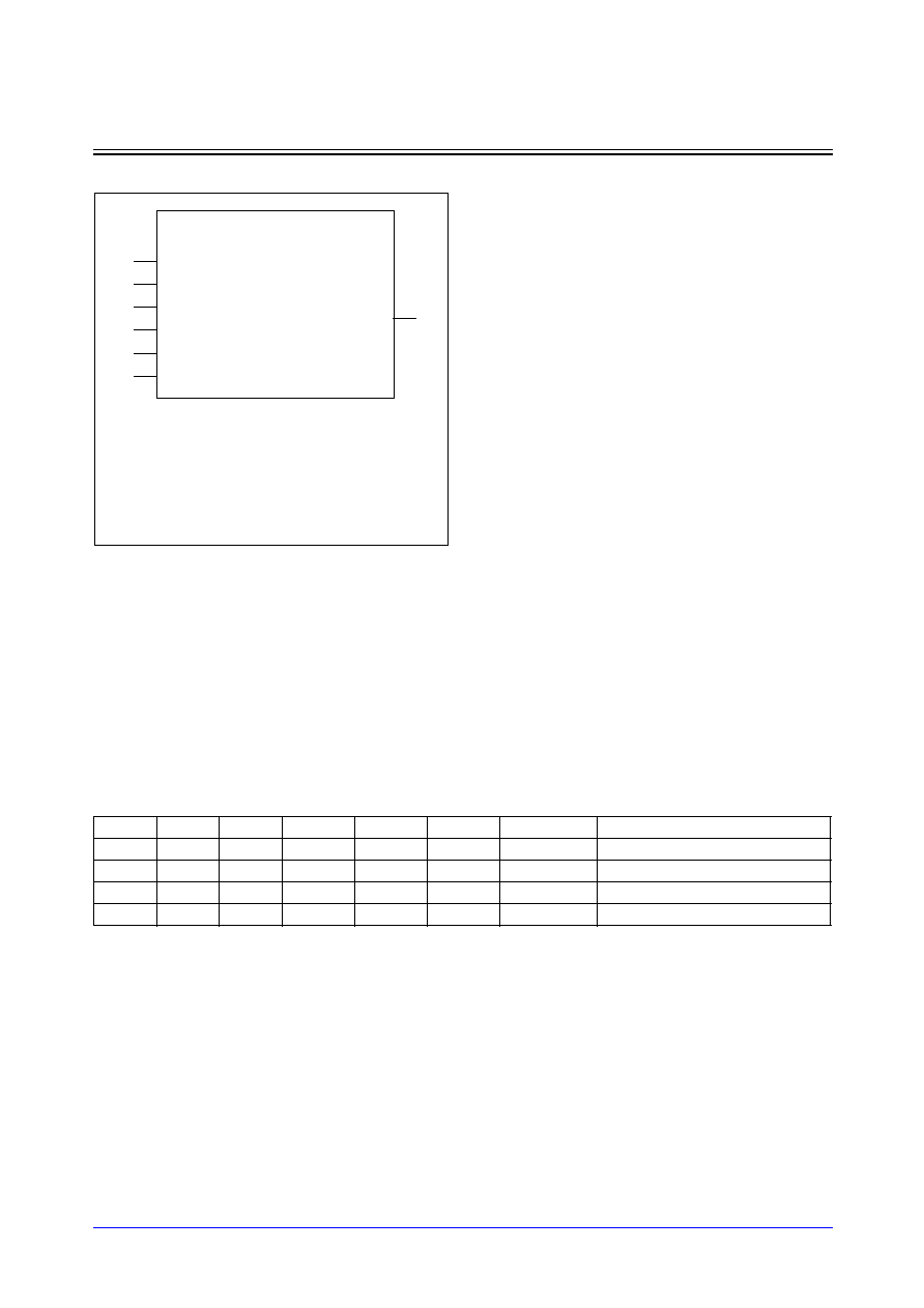
Samsung ASIC
5-9
STDL130
SPSRAM_HDL
High-Density Single-Port Synchronous Static RAM
Logic Symbol
Function Description
SPSRAM_HDL is a single-port synchronous static RAM which is provided as a compiler. SPSRAM_HDL is
intended for use in high-density applications. On the rising edge of CK, the write cycle is initiated when WEN
is low and CSN is low. The data on DI[] is written into the memory location specified on A[]. During the write
cycle, DOUT[] remains stable. On the rising edge of CK, the read cycle is initiated when WEN is high and
CSN is low. The data at DOUT[] become valid after a delay. While in standby mode that CSN is high, data
stored in the memory is retained and DOUT[] remains stable. When OEN is high, DOUT[] is placed in a
high-impedance state.
SPSRAM_HDL Function Table
Parameter Description
SPSRAM_HDL is the compiler that automatically generates symbol, netlist, timing model, power model and
layout according to the following parameters; Number of words(w), Number of bits per word(b), Column
mux(y) and Number of banks(ba).
CK
CSN
WEN
OEN
A
DI
DOUT
COMMENT
X
X
X
H
X
X
Z
Unconditional tri-state output
X
H
X
L
X
X
DOUT(t-1)
De-selected (standby mode)
L
L
L
Valid
Valid
DOUT(t-1)
Write cycle
L
H
L
Valid
X
MEM(A)
Read cycle
CK
CSN
WEN
OEN
A [m≠1:0]
spsram_hdl_<w>x<b>m<y>b<ba>
DOUT [b≠1:0]
DI [b≠1:0]
NOTES:
1. Words(w) is the number of words.
2. Bpw(b) is the number of bits per word.
3. Ymux(y) is one of the column mux types.
4. Banks(ba) is the number of banks.
5. m =
log
2
w
Features
∑
Suitable for high-density application
∑
Separated data I/O
∑
Synchronous operation
∑
Duty-free clock cycle
∑
Asynchronous tri-state output
∑
Latched inputs and outputs
∑
Automatic power-down
∑
Near zero hold time
∑
Low noise output optimization
∑
Flexible aspect ratio
∑
Dual-bank scheme available
∑
Up to 512Kbits capacity
∑
Up to 32K number of words
∑
Up to 128 number of bits per word
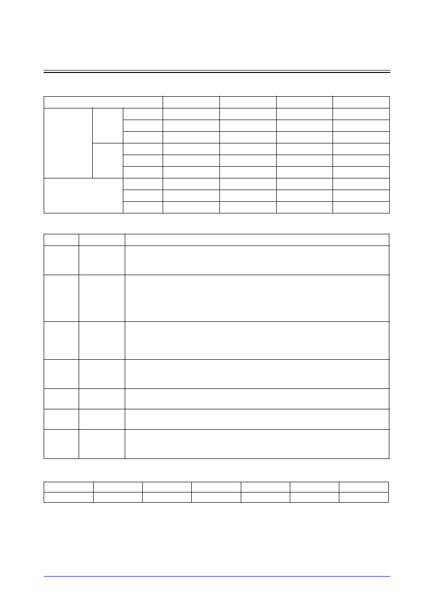
STDL130
5-10
Samsung ASIC
SPSRAM_HDL
High-Density Single-Port Synchronous Static RAM
Pin Descriptions
Pin Capacitance
Unit: [SL]
NOTE: Each pin's capacitance is exactly same regardless of available mux types for same bank.
Parameters
Ymux(y) = 4
Ymux(y) = 8
Ymux(y) = 16
Ymux(y) = 32
Words (w)
ba = 1
Min
32
64
128
256
Max
2048
4096
8192
16384
Step
16
32
64
128
ba = 2
Min
64
128
256
512
Max
4096
8192
16384
32768
Step
32
64
128
256
Bpw (b)
Min
1
1
1
1
Max
128
64
32
16
Step
1
1
1
1
Name
Type
Description
CK
Clock
Clock input. CSN, WEN, A[] and DI[] are latched into the RAM on the rising edge
of CK. If CSN and WEN are low on the rising edge of CK, the RAM is in write
mode. If WEN is high on the rising edge of CK, the RAM is in read mode.
CSN
Chip Enable Chip enable input. The chip enable is active-low and is latched into the RAM on
the rising edge of CK. When CSN is low, the RAM is enabled for reading or writ-
ing, depending on the state of WEN. When CSN is high, the RAM goes to the
standby mode and is disabled for reading or writing. DOUT remains previous
data output.
WEN
Read/Write
Enable
Read or write enable input. The read/write enable is latched into the RAM on the
rising edge of CK. When WEN is low, data are written to the addressed location
and DOUT remains stable. When WEN is high, data from the addressed word
are presented at DOUT.
OEN
Data Output
Enable
Data output enable input. The data output enable is asynchronously operated
regardless of any inputs. When OEN is high, DOUT is disabled and goes to
high-impedance state.
A [ ]
Address
Address input bus. The address is latched into the RAM on the rising edge of
CK.
DI [ ]
Data Input
Data input bus. Data are latched on the rising edge of CK. Data input is written
into the addressed location in write mode.
DOUT [ ] Data Output Data output bus. Data output is valid after the rising edge of CK while the RAM is
in read mode. Data output remains previous data output while the RAM is in
write mode.
CK
CSN
WEN
OEN
A
DI
DOUT
11.53
6.79
4.74
4.74
4.74
4.74
17.08
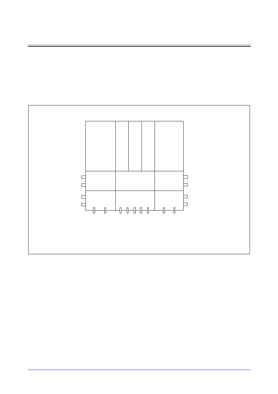
Samsung ASIC
5-11
STDL130
SPSRAM_HDL
High-Density Single-Port Synchronous Static RAM
Block Diagrams
SPSRAM_HDL has 2 different physical architectures due to the word depth. Optionally, one of these
architectures is generated from SPSRAM_HDL compiler. In dual-bank, the bank selected by the address is
only activated while the other bank is in idle mode. In 1-bank architecture, the power ports are located on the
middle-edge and the bottom edge of both right- and left-sides of the memory. In 2-bank architecture, the
power ports are located on the middle-edge and the bottom-edge of both right- and left-sides of the memory.
All signal ports are only located on the bottom sides of the memory regardless of architecture.
<1-bank architecture>
RAM Core
W
ord-line Decoder
X-Dec
W
ord-line Decoder
RAM Core
Y-Dec &
Sense Amp.
Control Block
Y-Dec &
Sense Amp.
I/O Driver
Address &
Clock Buffers
I/O Driver
VDD
VSS
VDD
VSS
VDD
VSS
VDD
VSS
DOUT[b-1:b/2]
DI[b-1:b/2]
A[m-1:0]
WEN
OEN
CSN
CK
DOUT[b/2-1:0]
DI[b/2-1:0]

STDL130
5-12
Samsung ASIC
SPSRAM_HDL
High-Density Single-Port Synchronous Static RAM
Application Notes
1.
Permitting over-the-cell routing.
In chip-level layout, over-the-cell routing in SPSRAM_HDL is permitted only for Metal-5 and Metal-6
layers.
2.
Incoming power bus should be adjusted to guarantee NOT more than 10% voltage drop at typical-case
current levels.
3.
Power stripe should be tapped from both sides of SPSRAM_HDL.
4.
Power reduction during standby mode.
The standby power is measured on the condition that only CSN is in disable mode and other signals are
in operation mode except that OEN is tied to low. If any of signals are activated while in standby mode,
the power will be consumed because the input switching activities are occurred by the signal transition.
Therefore, to reduce unnecessary power consumption, you should keep stable for all signals while in
standby mode.
<2-bank architecture >
RAM Core
W
ord-line
Decoder
X-Dec
W
ord-line
Decoder
RAM Core
Y-Dec &
Sense Amp.
Control Block
Y-Dec &
Sense Amp.
Y-Dec &
Sense Amp.
Control Block
Y-Dec &
Sense Amp.
RAM Core
W
ord-line
Decoder
X-Dec
W
ord-line
Decoder
RAM Core
I/O Driver
Address &
Clock Buffers
I/O Driver
VSS
VDD
VDD
VSS
VDD
VSS
VSS
VDD
VDD
VSS
VDD
VSS
DOUT[b/2-1:0]
DI[b/2-1:0]
A[m-1:0]
WEN
OEN
CSN
CK
DOUT[b-1:b/2]
DI[b-1:b/2]

Samsung ASIC
5-13
STDL130
SPSRAM_HDL
High-Density Single-Port Synchronous Static RAM
Characteristics
Definition for AC Timing (ns)
Symbol
Description
Symbol
Description
t
cyc
Clock cycle time
t
ckh
Clock pulse width high
t
ckl
Clock pulse width low
t
as
Address setup time
t
ah
Address hold time
t
cs
CSN setup time
t
ch
CSN hold time
t
ds
Data-In setup time
t
dh
Data-In hold time
t
ws
WEN setup time
t
wh
WEN hold time
t
acc
Data access time
t
da
De-access time
t
dz
DOUT drive to high-Z time
t
zd
DOUT high-Z to drive time
t
od
OEN to valid output time
Definition for Power Consumption (
µ
W/MHz)
Power_read
The dynamic average power consumption while in a read cycle
Power_write
The dynamic average power consumption while in a write cycle
Power_standby
The standby power consumption while CSN is high, OEN is low and other signals are in
normal operations.
Definition for Area (
µ
m)
Width
The physical width in X-direction
Height
The physical height in Y-direction
STDL130
5-14
Samsung ASIC
SPSRAM_HDL
High-Density Single-Port Synchronous Static RAM
Reference Table
* For Ymux=4
(Typical process, 1.8V, 25
∞
C, Output load=10SL, Input slope=0.2 ns, SA=0.5)
NOTE: Standby power is measured on condition that other signals are in normal operation while CSN is in disable
mode and OEN is low.
Parameters
words
128
128
256
256
512
512
768
768
bpw
32
32
48
48
64
64
80
80
ba
1
2
1
2
1
2
1
2
Timing (ns)
t
cyc
2.76
2.76
2.82
2.81
2.92
2.89
3.11
2.97
t
ckl
0.78
0.78
0.78
0.78
0.78
0.78
0.78
0.78
t
ckh
0.41
0.41
0.41
0.41
0.41
0.41
0.41
0.41
t
as
0.53
0.58
0.54
0.58
0.55
0.58
0.56
0.59
t
ah
0.23
0.23
0.23
0.23
0.23
0.23
0.23
0.23
t
cs
0.44
0.44
0.44
0.44
0.44
0.44
0.44
0.44
t
ch
0.01
0.01
0.01
0.01
0.01
0.01
0.01
0.01
t
ds
0.18
0.18
0.17
0.17
0.15
0.16
0.14
0.15
t
dh
0.17
0.17
0.19
0.19
0.20
0.20
0.22
0.22
t
ws
0.39
0.38
0.39
0.38
0.39
0.38
0.39
0.38
t
wh
0.23
0.22
0.22
0.22
0.22
0.22
0.22
0.22
t
acc
2.38
2.39
2.44
2.44
2.55
2.52
2.74
2.60
t
da
1.82
1.80
1.88
1.85
1.99
1.92
2.17
1.98
t
dz
0.21
0.21
0.22
0.22
0.24
0.24
0.25
0.25
t
zd
0.22
0.23
0.25
0.25
0.27
0.27
0.28
0.29
t
od
0.77
0.77
0.80
0.80
0.82
0.82
0.85
0.85
Power (
µ
W/MHz)
Power_read
142.92
157.33
201.95
218.13
266.87
283.21
333.79
353.99
Power_write
147.51
160.94
213.72
225.75
295.29
299.35
387.45
381.82
Power_standby
43.36
50.90
59.78
69.38
76.54
88.80
92.47
107.68
Area (
µ
m)
Width
337.28
337.28
456.04
456.04
574.80
574.80
693.56
693.56
Height
274.90
393.82
351.70
470.62
505.30
624.22
658.90
777.82

Samsung ASIC
5-15
STDL130
SPSRAM_HDL
High-Density Single-Port Synchronous Static RAM
Reference Table
* For Ymux=4
(Typical process, 1.8V, 25
∞
C, Output load=10SL, Input slope=0.2 ns, SA=0.5)
NOTE: Standby power is measured on condition that other signals are in normal operation while CSN is in disable
mode and OEN is low.
Parameters
words
1024
1024
1536
1536
2048
2048
4096
bpw
96
96
112
112
128
128
128
ba
1
2
1
2
1
2
2
Timing (ns)
t
cyc
3.31
3.05
3.64
3.27
3.68
3.50
4.01
t
ckl
0.78
0.78
0.78
0.78
0.78
0.78
0.78
t
ckh
0.41
0.41
0.41
0.41
0.41
0.41
0.41
t
as
0.57
0.59
0.58
0.59
0.59
0.59
0.59
t
ah
0.23
0.23
0.23
0.23
0.23
0.23
0.23
t
cs
0.44
0.44
0.44
0.44
0.44
0.44
0.44
t
ch
0.01
0.01
0.01
0.01
0.01
0.01
0.01
t
ds
0.13
0.14
0.12
0.13
0.11
0.11
0.11
t
dh
0.24
0.24
0.26
0.26
0.28
0.28
0.28
t
ws
0.39
0.38
0.39
0.38
0.39
0.38
0.35
t
wh
0.22
0.22
0.22
0.22
0.22
0.22
0.22
t
acc
2.94
2.68
3.28
2.90
3.31
3.13
3.64
t
da
2.36
2.05
2.69
2.24
2.72
2.45
2.85
t
dz
0.26
0.26
0.27
0.27
0.29
0.29
0.29
t
zd
0.30
0.30
0.32
0.32
0.33
0.33
0.33
t
od
0.88
0.88
0.90
0.90
0.93
0.93
0.93
Power (
µ
W/MHz)
Power_read
400.77
423.79
487.08
500.41
554.10
579.97
637.90
Power_write
486.61
466.56
627.73
574.55
773.90
692.54
847.50
Power_standby
109.16
128.13
125.99
150.32
142.60
173.15
187.80
Area (
µ
m)
Width
812.32
812.32
931.08
931.08
1049.84
1049.84
1049.84
Height
812.50
931.42
1119.70
1238.62
1426.90
1545.82
2774.62

STDL130
5-16
Samsung ASIC
SPSRAM_HDL
High-Density Single-Port Synchronous Static RAM
Reference Table
* For Ymux=8
(Typical process, 1.8V, 25
∞
C, Output load=10SL, Input slope=0.2 ns, SA=0.5)
NOTE: Standby power is measured on condition that other signals are in normal operation while CSN is in disable
mode and OEN is low.
Parameters
words
256
256
512
512
1024
1024
1536
1536
bpw
16
16
24
24
32
32
40
40
ba
1
2
1
2
1
2
1
2
Timing (ns)
t
cyc
2.76
2.77
2.82
2.82
2.93
2.89
3.12
2.97
t
ckl
0.78
0.78
0.78
0.78
0.78
0.78
0.78
0.78
t
ckh
0.41
0.41
0.41
0.41
0.41
0.41
0.41
0.41
t
as
0.53
0.58
0.54
0.58
0.55
0.58
0.56
0.59
t
ah
0.23
0.23
0.23
0.23
0.23
0.23
0.23
0.23
t
cs
0.44
0.44
0.44
0.44
0.44
0.44
0.44
0.44
t
ch
0.01
0.01
0.01
0.01
0.01
0.01
0.01
0.01
t
ds
0.19
0.19
0.18
0.18
0.17
0.17
0.16
0.16
t
dh
0.16
0.16
0.17
0.17
0.18
0.18
0.20
0.20
t
ws
0.39
0.38
0.39
0.38
0.39
0.38
0.39
0.38
t
wh
0.23
0.23
0.22
0.22
0.22
0.22
0.22
0.22
t
acc
2.39
2.40
2.45
2.44
2.55
2.52
2.74
2.60
t
da
1.83
1.81
1.89
1.85
1.99
1.92
2.17
1.98
t
dz
0.20
0.20
0.21
0.21
0.22
0.22
0.23
0.23
t
zd
0.21
0.21
0.23
0.23
0.24
0.24
0.25
0.25
t
od
0.75
0.75
0.77
0.77
0.79
0.79
0.81
0.81
Power (
µ
W/MHz)
Power_read
115.89
128.12
161.52
174.14
213.41
224.08
267.64
280.42
Power_write
121.97
135.55
172.91
186.19
234.13
242.76
302.94
307.23
Power_standby
28.42
35.49
37.37
46.13
46.68
57.38
55.09
68.02
Area (
µ
m)
Width
337.28
337.28
456.04
456.04
574.80
574.80
693.56
693.56
Height
210.60
300.76
287.40
377.56
441.00
531.16
594.60
684.76
Samsung ASIC
5-17
STDL130
SPSRAM_HDL
High-Density Single-Port Synchronous Static RAM
Reference Table
* For Ymux=8
(Typical process, 1.8V, 25
∞
C, Output load=10SL, Input slope=0.2 ns, SA=0.5)
NOTE: Standby power is measured on condition that other signals are in normal operation while CSN is in disable
mode and OEN is low.
Parameters
words
2048
2048
3072
3072
4096
4096
8192
bpw
48
48
56
56
64
64
64
ba
1
2
1
2
1
2
2
Timing (ns)
t
cyc
3.32
3.05
3.64
3.27
3.69
3.50
4.01
t
ckl
0.78
0.78
0.78
0.78
0.79
0.78
0.78
t
ckh
0.41
0.41
0.41
0.41
0.41
0.41
0.41
t
as
0.57
0.59
0.58
0.59
0.59
0.59
0.59
t
ah
0.23
0.23
0.23
0.23
0.23
0.23
0.23
t
cs
0.44
0.44
0.44
0.44
0.44
0.44
0.44
t
ch
0.01
0.01
0.01
0.01
0.01
0.01
0.01
t
ds
0.16
0.16
0.15
0.15
0.14
0.14
0.14
t
dh
0.21
0.21
0.22
0.22
0.24
0.24
0.24
t
ws
0.39
0.38
0.39
0.38
0.39
0.38
0.35
t
wh
0.22
0.22
0.22
0.22
0.22
0.22
0.22
t
acc
2.94
2.67
3.27
2.90
3.31
3.13
3.64
t
da
2.37
2.04
2.69
2.24
2.72
2.45
2.85
t
dz
0.24
0.24
0.25
0.25
0.25
0.25
0.25
t
zd
0.26
0.27
0.28
0.28
0.29
0.29
0.29
t
od
0.83
0.83
0.84
0.84
0.86
0.86
0.86
Power (
µ
W/MHz)
Power_read
320.61
334.59
392.94
394.03
447.00
455.58
503.90
Power_write
373.67
370.59
472.29
447.52
566.60
530.31
623.00
Power_standby
64.35
79.89
73.53
92.67
82.77
105.83
113.90
Area (
µ
m)
Width
812.32
812.32
931.08
931.08
1049.84
1049.84
1049.84
Height
748.20
838.36
1055.40
1145.56
1362.60
1452.76
2681.56

STDL130
5-18
Samsung ASIC
SPSRAM_HDL
High-Density Single-Port Synchronous Static RAM
Reference Table
* For Ymux=16
(Typical process, 1.8V, 25
∞
C, Output load=10SL, Input slope=0.2 ns, SA=0.5)
NOTE: Standby power is measured on condition that other signals are in normal operation while CSN is in disable
mode and OEN is low.
Parameters
words
512
512
1024
1024
2048
2048
3072
3072
bpw
8
8
12
12
16
16
20
20
ba
1
2
1
2
1
2
1
2
Timing (ns)
t
cyc
2.78
2.81
2.84
2.85
2.95
2.93
3.14
3.01
t
ckl
0.78
0.78
0.78
0.78
0.78
0.78
0.78
0.78
t
ckh
0.41
0.41
0.41
0.41
0.41
0.41
0.41
0.41
t
as
0.53
0.58
0.54
0.58
0.55
0.58
0.56
0.59
t
ah
0.23
0.23
0.23
0.23
0.23
0.23
0.23
0.23
t
cs
0.44
0.44
0.44
0.44
0.44
0.44
0.44
0.44
t
ch
0.01
0.01
0.01
0.01
0.01
0.01
0.01
0.01
t
ds
0.19
0.20
0.19
0.19
0.18
0.18
0.17
0.17
t
dh
0.16
0.16
0.17
0.16
0.17
0.17
0.19
0.18
t
ws
0.39
0.38
0.39
0.38
0.39
0.38
0.38
0.38
t
wh
0.23
0.23
0.22
0.22
0.22
0.22
0.23
0.22
t
acc
2.41
2.43
2.47
2.48
2.57
2.56
2.76
2.64
t
da
1.83
1.81
1.89
1.85
1.99
1.92
2.17
1.98
t
dz
0.19
0.19
0.20
0.20
0.21
0.21
0.22
0.22
t
zd
0.21
0.21
0.22
0.22
0.22
0.23
0.24
0.24
t
od
0.75
0.75
0.76
0.76
0.77
0.77
0.79
0.79
Power (
µ
W/MHz)
Power_read
87.90
100.11
119.43
132.00
157.04
167.59
197.52
209.08
Power_write
90.00
103.74
123.54
137.73
164.68
176.19
211.42
221.12
Power_standby
22.05
28.83
27.82
36.06
33.94
43.73
39.02
50.43
Area (
µ
m)
Width
337.28
337.28
456.04
456.04
574.80
574.78
693.56
693.56
Height
210.60
300.76
287.40
377.56
441.00
531.16
594.60
684.76

Samsung ASIC
5-19
STDL130
SPSRAM_HDL
High-Density Single-Port Synchronous Static RAM
Reference Table
* For Ymux=16
(Typical process, 1.8V, 25
∞
C, Output load=10SL, Input slope=0.2 ns, SA=0.5)
NOTE: Standby power is measured on condition that other signals are in normal operation while CSN is in disable
mode and OEN is low.
Parameters
words
4096
4096
6144
6144
8192
8192
16384
bpw
24
24
28
28
32
32
32
ba
1
2
1
2
1
2
2
Timing (ns)
t
cyc
3.34
3.09
3.67
3.30
3.70
3.54
4.04
t
ckl
0.78
0.78
0.78
0.78
0.78
0.78
0.78
t
ckh
0.41
0.41
0.42
0.41
0.41
0.41
0.41
t
as
0.56
0.59
0.57
0.59
0.59
0.59
0.59
t
ah
0.23
0.23
0.24
0.23
0.23
0.23
0.23
t
cs
0.44
0.44
0.44
0.44
0.44
0.44
0.44
t
ch
0.01
0.01
0.01
0.01
0.01
0.01
0.01
t
ds
0.16
0.17
0.15
0.16
0.16
0.16
0.16
t
dh
0.20
0.19
0.22
0.20
0.21
0.21
0.21
t
ws
0.38
0.38
0.37
0.38
0.39
0.38
0.35
t
wh
0.23
0.22
0.23
0.22
0.22
0.22
0.22
t
acc
2.96
2.71
3.29
2.93
3.33
3.17
3.67
t
da
2.37
2.04
2.69
2.24
2.72
2.45
2.85
t
dz
0.22
0.22
0.23
0.23
0.24
0.24
0.24
t
zd
0.24
0.25
0.25
0.25
0.26
0.26
0.26
t
od
0.80
0.80
0.81
0.81
0.83
0.83
0.83
Power (
µ
W/MHz)
Power_read
236.66
248.58
294.99
292.89
334.10
339.11
382.90
Power_write
258.62
264.40
325.95
316.89
384.20
373.19
434.40
Power_standby
45.15
58.64
51.23
67.22
54.47
75.94
80.95
Area (
µ
m)
Width
812.32
812.32
931.08
931.08
1049.84
1049.84
1049.84
Height
748.20
838.36
1055.40
1145.56
1362.60
1452.76
2681.56

STDL130
5-20
Samsung ASIC
SPSRAM_HDL
High-Density Single-Port Synchronous Static RAM
Reference Table
* For Ymux=32
(Typical process, 1.8V, 25
∞
C, Output load=10SL, Input slope=0.2 ns, SA=0.5)
NOTE: Standby power is measured on condition that other signals are in normal operation while CSN is in disable
mode and OEN is low.
Parameters
words
1024
1024
2048
2048
4096
4096
6144
6144
bpw
4
4
6
6
8
8
10
10
ba
1
2
1
2
1
2
1
2
Timing (ns)
t
cyc
2.82
2.88
2.88
2.92
3.00
3.00
3.17
3.07
t
ckl
0.78
0.78
0.78
0.78
0.78
0.78
0.78
0.78
t
ckh
0.41
0.41
0.41
0.41
0.41
0.41
0.41
0.41
t
as
0.53
0.58
0.54
0.58
0.55
0.58
0.56
0.59
t
ah
0.23
0.23
0.23
0.23
0.23
0.23
0.23
0.23
t
cs
0.44
0.44
0.44
0.44
0.44
0.44
0.44
0.44
t
ch
0.01
0.01
0.01
0.01
0.01
0.01
0.01
0.01
t
ds
0.20
0.20
0.19
0.19
0.18
0.18
0.18
0.18
t
dh
0.15
0.15
0.16
0.16
0.17
0.17
0.18
0.18
t
ws
0.39
0.38
0.39
0.38
0.39
0.38
0.39
0.38
t
wh
0.23
0.23
0.22
0.22
0.22
0.22
0.22
0.22
t
acc
2.45
2.50
2.51
2.55
2.62
2.63
2.80
2.71
t
da
1.83
1.81
1.89
1.85
1.99
1.92
2.17
1.98
t
dz
0.19
0.19
0.20
0.20
0.20
0.20
0.21
0.21
t
zd
0.20
0.20
0.21
0.21
0.22
0.22
0.23
0.23
t
od
0.74
0.74
0.75
0.75
0.76
0.76
0.78
0.78
Power (
µ
W/MHz)
Power_read
73.89
85.99
98.33
110.74
128.92
139.15
162.33
173.07
Power_write
73.64
87.51
98.14
112.86
128.81
141.89
163.90
176.34
Power_standby
18.35
24.98
22.28
30.23
26.55
35.84
29.50
39.89
Area (
µ
m)
Width
337.28
337.28
456.04
456.04
574.80
574.80
693.56
693.56
Height
210.60
300.76
287.40
377.56
441.00
531.16
594.60
684.76

Samsung ASIC
5-21
STDL130
SPSRAM_HDL
High-Density Single-Port Synchronous Static RAM
Reference Table
* For Ymux=32
(Typical process, 1.8V, 25
∞
C, Output load=10SL, Input slope=0.2 ns, SA=0.5)
NOTE: Standby power is measured on condition that other signals are in normal operation while CSN is in disable
mode and OEN is low.
Parameters
words
8192
8192
12288
12288
16384
16384
32768
bpw
12
12
14
14
16
16
16
ba
1
2
1
2
1
2
2
Timing (ns)
t
cyc
3.37
3.15
3.71
3.37
3.74
3.60
4.11
t
ckl
0.78
0.78
0.78
0.78
0.78
0.78
0.78
t
ckh
0.41
0.41
0.41
0.41
0.41
0.41
0.41
t
as
0.57
0.59
0.58
0.59
0.59
0.59
0.59
t
ah
0.23
0.23
0.23
0.23
0.23
0.23
0.23
t
cs
0.44
0.44
0.44
0.44
0.44
0.44
0.44
t
ch
0.01
0.01
0.01
0.01
0.01
0.01
0.01
t
ds
0.17
0.17
0.17
0.17
0.16
0.16
0.16
t
dh
0.19
0.19
0.20
0.19
0.20
0.20
0.20
t
ws
0.39
0.38
0.39
0.38
0.39
0.38
0.35
t
wh
0.22
0.22
0.22
0.22
0.22
0.22
0.22
t
acc
3.00
2.78
3.33
3.00
3.37
3.24
3.74
t
da
2.37
2.04
2.69
2.24
2.72
2.45
2.85
t
dz
0.22
0.22
0.22
0.22
0.23
0.23
0.23
t
zd
0.24
0.24
0.24
0.24
0.25
0.25
0.25
t
od
0.79
0.79
0.80
0.80
0.81
0.81
0.81
Power (
µ
W/MHz)
Power_read
194.55
205.42
246.16
242.31
278.50
280.88
321.80
Power_write
199.19
209.62
251.06
249.72
291.20
292.51
337.50
Power_standby
33.10
46.14
38.26
52.54
42.62
58.96
62.26
Area (
µ
m)
Width
812.32
812.32
931.08
931.08
1049.84
1049.84
1049.84
Height
748.20
838.36
1055.40
1145.56
1362.60
1452.76
2681.56

STDL130
5-22
Samsung ASIC
SPSRAM_HDL
High-Density Single-Port Synchronous Static RAM
Timing Diagrams
Read Cycle
Write Cycle
t
as
A[]
t
ah
(CSN = low, OEN = low, DI = don't care)
t
acc
WEN
t
ws
t
wh
t
da
DOUT[]
t
cyc
CK
t
ckl
t
ckh
A0
A2
Valid
M[A0]
M[A1]
M[A2]
A1
t
as
A[]
t
ah
(CSN= low, OEN = don't care)
WEN
t
ws
t
wh
DI[]
t
cyc
CK
t
ckl
t
ckh
A0
A2
A1
t
ds
t
dh
D0
D2
D1
Samsung ASIC
5-23
STDL130
SPSRAM_HDL
High-Density Single-Port Synchronous Static RAM
Read Cycle with CSN Controlled
OEN Controlled Output Enable
NOTE: "don't care" means the condition that these pins are in normal operation mode.
t
as
A[]
t
ah
(OEN = low, WEN = high, DI = don't care)
CSN
t
cs
t
ch
DOUT[]
t
cyc
CK
t
ckl
t
ckh
A0
A2
A1
t
da
t
acc
M[A1]
M[A0]
(CK, A, WEN, DI, CSN = don't care)
t
od
t
dz
Hi-Z
VALID
OEN
DOUT[]
Hi-Z
t
zd

STDL130
5-24
Samsung ASIC
SPSRAMBW_HDL
High-Density Single-Port Synchronous Static RAM with Bit-Write
Logic Symbol
Function Description
SPSRAMBW_HDL is a single-port synchronous static RAM with bit-write capability which is provided as a
compiler. SPSRAMBW_HDL is intended for use in high-density applications. Basically, its functionality is
exactly same as SPSRAM_HDL except a bit-write operation which is controlled by BWEN[], named bit-write
enable signal bus. Each bit of BWEN[] enables or disables the write operation of its corresponding bit in DI[].
On the rising edge of CK, the write cycle is initiated when WEN is low and CSN is low. The data bits in DI[],
which their corresponding bit(s) in BWEN[] are low, are written into the memory location specified on A[].
When all bits of BWEN[] are high, any data in DI[] are not written into the memory location specified on A[].
When all bits of BWEN[] are low, the data in DI[] are written into the memory location specified on A[], which
is exactly same as the write operation in SPSRAM_HDL. During the write cycle, DOUT[] remains stable. On
the rising edge of CK, the read cycle is initiated when WEN is high and CSN is low. The data at DOUT[]
become valid after a delay. While in standby mode that CSN is high, A[] and DI[] are disabled, data stored in
the memory is retained and DOUT[] remains stable. When OEN is high, DOUT[] is placed in a
high-impedance state.
SPSRAMBW_HDL Function Table
CK
CSN
WEN
OEN
A
BWEN
DI
DOUT
Comment
X
X
X
H
X
X
X
Z
Unconditional tri-state output
X
H
X
L
X
X
X
DOUT(t-1)
De-selected (standby mode)
L
L
L
Valid
all L
Valid
DOUT(t-1)
Word-write cycle
L
L
L
Valid
L
Valid
DOUT(t-1)
Bit-write cycle
L
L
L
Valid
all H
Valid
DOUT(t-1)
No operation
L
H
L
Valid
X
X
MEM(A)
Read Cycle
Features
∑
Suitable for high-density application
∑
Bit-write capability
∑
Separated data I/O
∑
Synchronous operation
∑
Duty-free clock cycle
∑
Asynchronous tristate output
∑
Latched inputs and outputs
∑
Automatic power-down
∑
Near zero hold time
∑
Low noise output optimization
∑
Flexible aspect ratio
∑
Dual-bank scheme available
∑
Up to 512Kbits capacity
∑
Up to 32K number of words
∑
Up to128 number of bit per word
CK
CSN
WEN
BWEN [b-1:0]
OEN
spsrambw_hdl_<w>x<b>m<y>b<ba>
DOUT [b-1:0]
A [m-1:0]
NOTES:
1. Words(w) is the number of words.
2. Bpw(b) is the number of bits per word.
3. Ymux(y) is one of the column mux types.
4. Banks(ba) is the number of banks.
DI [b-1:0]
5. m =
log
2
w
Samsung ASIC
5-25
STDL130
SPSRAMBW_HDL
High-Density Single-Port Synchronous Static RAM with Bit-Write
Parameter Description
SPSRAMBW_HDL is the compiler that automatically generates symbol, netlist, timing model, power model
and layout according to the following parameters; Number of words(w), Number of bits per word(b), Column
mux(y) and Number of banks(ba)
Pin Descriptions
Parameters
Ymux(y) = 4
Ymux(y) = 8
Ymux(y) = 16
Ymux(y) = 32
Words (w)
ba = 1
Min
32
64
128
256
Max
2048
4096
8192
16384
Step
16
32
64
128
ba = 2
Min
64
128
256
512
Max
4096
8192
16384
32768
Step
32
64
128
256
Bpw (b)
Min
2
2
2
2
Max
128
64
32
16
Step
1
1
1
1
Name
Type
Description
CK
Clock
Clock input. CSN, WEN, A[] and DI[] are latched into the RAM on the rising edge
of CK. If CSN and WEN are low on the rising edge of CK, the RAM is in write
mode. If WEN is high on the rising edge of CK, the RAM is in read mode.
CSN
Chip Enable Chip enable input. The chip enable is active-low and is latched into the RAM on
the rising edge of CK. When CSN is low, the RAM is enabled for reading or writ-
ing, depending on the state of WEN. When CSN is high, the RAM goes to the
standby mode and is disabled for reading or writing. DOUT remains previous
data output.
WEN
Read/Write
Enable
Read or write enable input. The read/write enable is latched into the RAM on the
rising edge of CK. When WEN is low, data are written to the addressed location
and DOUT remains stable. When WEN is high, data from the addressed word
are presented at DOUT.
BWEN[]
Bit-Write
Enable
Bit-write enable input bus. The bit-write enable is latched into the RAM on the
rising edge of CK. Each bit of BWEN[] enables/disables the write operation of
corresponding data bit. BWEN[i] corresponds to DI[i] in bit-write. If WEN and
BWEN[0] are low and BWEN[1] is high, DI[0] is written into the memory location
specified on A[], but DI[1] is not written.
OEN
Data Output
Enable
Data output enable input. The data output enable is asynchronously operated
regardless of any input. When OEN is high, DOUT is disabled and goes to
high-impedance state.
A[]
Address
Address input bus. The address is latched into the RAM on the rising edge of
CK.
DI[]
Data Input
Data input bus. Data are latched on the rising edge of CK. Data input is written
into the addressed location in write mode.
DOUT[]
Data Output Data output bus. Data output is valid after the rising edge of CK while the RAM is
in read mode. Data output remains previous data output while the RAM is in
write mode.
STDL130
5-26
Samsung ASIC
SPSRAMBW_HDL
High-Density Single-Port Synchronous Static RAM with Bit-Write
Pin Capacitance
Unit: [SL]
NOTE: Each pin's capacitance is exactly same regardless of available mux types for same bank.
Block Diagrams
SPSRAMBW_HDL has 2 different physical architectures due to the word depth. Optionally, one of these
architectures is generated from SPSRAMBW_HDL compiler. In dual-bank, the bank selected by the address
is only activated while the other bank is in idle mode. In 1-bank architecture, the power ports are located on
the middle-edge and the bottom edge of both right- and left-sides of the memory. In 2-bank architecture, the
power ports are located on the middle-edge and the bottom-edge of both right- and left-sides of the memory.
All signal ports are only located on the bottom sides of the memory regardless of architecture.
CK
CSN
WEN
BWEN
OEN
A
DI
DOUT
11.53
6.79
4.74
4.74
4.74
4.74
4.74
17.08
<1-bank architecture>
RAM Core
W
ord-line Decoder
X-Dec
W
ord-line Decoder
RAM Core
Y-Dec &
Sense Amp.
Control Block
Y-Dec &
Sense Amp.
I/O Driver
Address &
Clock Buffers
I/O Driver
VDD
VSS
VDD
VSS
VDD
VSS
VDD
VSS
DOUT[b/2-1:0]
DI[b/2-1:0]
A[m-1:0]
WEN
OEN
CSN
CK
DOUT[b-1:b/2]
DI[b-1:b/2]
BWEN[b-1:b/2]
BWEN[b/2-1:0]
Samsung ASIC
5-27
STDL130
SPSRAMBW_HDL
High-Density Single-Port Synchronous Static RAM with Bit-Write
Application Notes
1.
Permitting Over-the-cell routing
In chip-level layout, over-the-cell routing in SPSRAMBW_HDL is permitted for only Metal-5 and Metal-6
layers.
2.
Incoming power bus should be adjusted to guarantee NOT more than 10% voltage drop at typical-case
current levels.
3.
Power stripe should be tapped from both sides of SPSRAMBW_HDL.
4.
A byte-write or word-write operation with SPSRAMBW_HDL.
Refer to the function table. In byte-write operation, the number of BWEN[] signal bus should be divided
by a byte (8) and eight BWEN signals should be tied to a connection wire. In this case, DI[] bus is
controlled by a byte-wired BWEN signal instead of each BWEN bit. In word-write operation, the
functionality is exactly same as SPSRAM_HDL. If all of BWEN[] signal is tied to low state, DI[] bus is
only controlled by WEN.
5.
Power reduction during standby mode.
The standby power is measured on the condition that only CSN is in disable mode and other signals are
in operation mode except that OEN is tied to low. If any of signals are activated while in standby mode,
the power will be consumed because the input switching activities are occurred by the signal transition.
Therefore, to reduce unnecessary power consumption, you should keep stable for all signals while in
standby mode.
<2-bank architecture >
RAM Core
W
ord-line
Decoder
X-Dec
W
ord-line
Decoder
RAM Core
Y-Dec &
Sense Amp.
Control Block
Y-Dec &
Sense Amp.
Y-Dec &
Sense Amp.
Control Block
Y-Dec &
Sense Amp.
RAM Core
W
ord-line
Decoder
X-Dec
W
ord-line
Decoder
RAM Core
I/O Driver
Address &
Clock Buffers
I/O Driver
VSS
VDD
VDD
VSS
VDD
VSS
VSS
VDD
VDD
VSS
VDD
VSS
DOUT[b/2-1:0]
DI[b/2-1:0]
A[m-1:0]
WEN
OEN
CSN
CK
DOUT[b-1:b/2]
DI[b-1:b/2]
BWEN[b-1:b/2]
BWEN[b/2-1:0]

STDL130
5-28
Samsung ASIC
SPSRAMBW_HDL
High-Density Single-Port Synchronous Static RAM with Bit-Write
Characteristics
Definition for AC Timing (ns)
Symbol
Description
Symbol
Description
t
cyc
Clock cycle time
t
ckh
Clock pulse width high
t
ckl
Clock pulse width low
t
as
Address setup time
t
ah
Address hold time
t
cs
CSN setup time
t
ch
CSN hold time
t
ds
Data-In setup time
t
dh
Data-In hold time
t
ws
WEN setup time
t
wh
WEN hold time
t
bws
BWEN setup time
t
bwh
BWEN hold time
t
acc
Data access time
t
da
De-access time
t
dz
DOUT drive to high-Z time
t
zd
DOUT high-Z to drive time
t
od
OEN to valid output time
Definition for Power Consumption (
µ
W/MHz)
Power_read
The dynamic average power consumption while in a read cycle
Power_write
The dynamic average power consumption while in a write cycle
Power_standby
The standby power consumption while CSN is high, OEN is low and other signals are in
normal operations.
Definition for Area (
µ
m)
Width
The physical width in X-direction
Height
The physical height in Y-direction

Samsung ASIC
5-29
STDL130
SPSRAMBW_HDL
High-Density Single-Port Synchronous Static RAM with Bit-Write
Reference Table
* For Ymux=4
(Typical process, 1.8V, 25
∞
C, Output load=10SL, Input slope=0.2 ns, SA=0.5)
NOTE: Standby power is measured on condition that other signals are in normal operation while CSN is in disable
mode and OEN is low.
Parameters
words
128
128
256
256
512
512
768
768
bpw
32
32
48
48
64
64
80
80
ba
1
2
1
2
1
2
1
2
Timing (ns)
t
cyc
2.76
2.76
2.82
2.81
2.92
2.89
3.11
2.97
t
ckl
0.78
0.78
0.78
0.78
0.78
0.78
0.78
0.78
t
ckh
0.41
0.41
0.41
0.41
0.41
0.41
0.41
0.41
t
as
0.53
0.58
0.54
0.58
0.55
0.58
0.56
0.59
t
ah
0.23
0.23
0.23
0.23
0.23
0.23
0.23
0.23
t
cs
0.44
0.44
0.44
0.44
0.44
0.44
0.44
0.44
t
ch
0.01
0.01
0.01
0.01
0.01
0.01
0.01
0.01
t
ds
0.18
0.18
0.17
0.17
0.15
0.16
0.14
0.15
t
dh
0.17
0.17
0.19
0.19
0.20
0.20
0.22
0.22
t
ws
0.39
0.38
0.39
0.38
0.39
0.38
0.39
0.38
t
wh
0.23
0.22
0.22
0.22
0.22
0.22
0.22
0.22
t
bws
0.18
0.18
0.17
0.17
0.15
0.17
0.14
0.17
t
bwh
0.15
0.15
0.17
0.17
0.19
0.19
0.20
0.20
t
acc
2.38
2.39
2.44
2.44
2.55
2.52
2.74
2.60
t
da
1.82
1.80
1.88
1.85
1.99
1.92
2.17
1.98
t
dz
0.21
0.21
0.22
0.22
0.24
0.24
0.25
0.25
t
zd
0.22
0.23
0.25
0.25
0.27
0.27
0.28
0.29
t
od
0.77
0.77
0.80
0.80
0.82
0.82
0.85
0.85
Power (
µ
W/MHz)
Power_read
149.56
163.93
212.12
228.26
280.56
296.88
350.76
371.13
Power_write
154.13
167.56
223.87
235.91
308.95
313.05
404.47
398.99
Power_standby
49.98
57.51
69.92
79.53
90.21
102.49
109.47
124.82
Area (
µ
m)
Width
337.28
337.28
456.04
456.04
574.80
574.80
693.56
693.56
Height
274.90
393.82
351.70
470.62
505.30
624.22
658.90
777.82

STDL130
5-30
Samsung ASIC
SPSRAMBW_HDL
High-Density Single-Port Synchronous Static RAM with Bit-Write
Reference Table
* For Ymux=4
(Typical process, 1.8V, 25
∞
C, Output load=10SL, Input slope=0.2 ns, SA=0.5)
NOTE: Standby power is measured on condition that other signals are in normal operation while CSN is in disable
mode and OEN is low.
Parameters
words
1024
1024
1536
1536
2048
2048
4096
bpw
96
96
112
112
128
128
128
ba
1
2
1
2
1
2
2
Timing (ns)
t
cyc
3.31
3.05
3.64
3.27
3.68
3.50
4.01
t
ckl
0.78
0.78
0.78
0.78
0.78
0.78
0.78
t
ckh
0.41
0.41
0.41
0.41
0.41
0.41
0.41
t
as
0.57
0.59
0.58
0.59
0.59
0.59
0.59
t
ah
0.23
0.23
0.23
0.23
0.23
0.23
0.23
t
cs
0.44
0.44
0.44
0.44
0.44
0.44
0.44
t
ch
0.01
0.01
0.01
0.01
0.01
0.01
0.01
t
ds
0.13
0.14
0.12
0.13
0.11
0.11
0.11
t
dh
0.24
0.24
0.26
0.26
0.28
0.28
0.28
t
ws
0.39
0.38
0.39
0.38
0.39
0.38
0.35
t
wh
0.22
0.22
0.22
0.22
0.22
0.22
0.22
t
bws
0.13
0.17
0.12
0.18
0.11
0.19
0.25
t
bwh
0.22
0.22
0.24
0.24
0.26
0.26
0.26
t
acc
2.94
2.68
3.28
2.90
3.31
3.13
3.64
t
da
2.36
2.05
2.69
2.24
2.72
2.45
2.85
t
dz
0.26
0.26
0.27
0.27
0.29
0.29
0.29
t
zd
0.30
0.30
0.32
0.32
0.33
0.33
0.33
t
od
0.88
0.88
0.90
0.90
0.93
0.93
0.93
Power (
µ
W/MHz)
Power_read
421.34
444.55
511.18
524.83
581.85
608.05
666.40
Power_write
507.19
487.37
651.81
598.99
801.67
720.66
876.01
Power_standby
129.75
148.89
150.10
174.75
170.32
201.31
216.24
Area (
µ
m)
Width
812.32
812.32
931.08
931.08
1049.84
1049.84
1049.84
Height
812.50
931.42
1119.70
1238.62
1426.90
1545.82
2774.62

Samsung ASIC
5-31
STDL130
SPSRAMBW_HDL
High-Density Single-Port Synchronous Static RAM with Bit-Write
Reference Table
* For Ymux=8
(Typical process, 1.8V, 25
∞
C, Output load=10SL, Input slope=0.2 ns, SA=0.5)
NOTE: Standby power is measured on condition that other signals are in normal operation while CSN is in disable
mode and OEN is low.
Parameters
words
256
256
512
512
1024
1024
1536
1536
bpw
16
16
24
24
32
32
40
40
ba
1
2
1
2
1
2
1
2
Timing (ns)
t
cyc
2.76
2.77
2.82
2.82
2.93
2.89
3.12
2.97
t
ckl
0.78
0.78
0.78
0.78
0.78
0.78
0.78
0.78
t
ckh
0.41
0.41
0.41
0.41
0.41
0.41
0.41
0.41
t
as
0.53
0.58
0.54
0.58
0.55
0.58
0.56
0.59
t
ah
0.23
0.23
0.23
0.23
0.23
0.23
0.23
0.23
t
cs
0.44
0.44
0.44
0.44
0.44
0.44
0.44
0.44
t
ch
0.01
0.01
0.01
0.01
0.01
0.01
0.01
0.01
t
ds
0.19
0.19
0.18
0.18
0.17
0.17
0.16
0.16
t
dh
0.16
0.16
0.17
0.17
0.18
0.18
0.20
0.20
t
ws
0.39
0.38
0.39
0.38
0.39
0.38
0.39
0.38
t
wh
0.23
0.23
0.22
0.22
0.22
0.22
0.22
0.22
t
bws
0.19
0.19
0.17
0.18
0.15
0.18
0.15
0.19
t
bwh
0.14
0.14
0.15
0.15
0.17
0.17
0.18
0.18
t
acc
2.39
2.40
2.45
2.44
2.55
2.52
2.74
2.60
t
da
1.83
1.81
1.89
1.85
1.99
1.92
2.17
1.98
t
dz
0.20
0.20
0.21
0.21
0.22
0.22
0.23
0.23
t
zd
0.21
0.21
0.23
0.23
0.24
0.24
0.25
0.25
t
od
0.75
0.75
0.77
0.77
0.79
0.79
0.81
0.81
Power (
µ
W/MHz)
Power_read
118.96
131.20
166.33
178.98
219.97
230.70
275.80
288.66
Power_write
125.05
138.65
177.76
191.07
240.76
249.42
311.14
315.46
Power_standby
31.50
38.58
42.22
50.99
53.29
64.02
63.28
76.29
Area (
µ
m)
Width
337.28
337.28
456.04
456.04
574.80
574.80
693.56
693.56
Height
210.60
300.76
287.40
377.56
441.00
531.16
594.60
684.76

STDL130
5-32
Samsung ASIC
SPSRAMBW_HDL
High-Density Single-Port Synchronous Static RAM with Bit-Write
Reference Table
* For Ymux=8
(Typical process, 1.8V, 25
∞
C, Output load=10SL, Input slope=0.2 ns, SA=0.5)
NOTE: Standby power is measured on condition that other signals are in normal operation while CSN is in disable
mode and OEN is low.
Parameters
words
2048
2048
3072
3072
4096
4096
8192
bpw
48
48
56
56
64
64
64
ba
1
2
1
2
1
2
2
Timing (ns)
t
cyc
3.32
3.05
3.64
3.27
3.69
3.50
4.01
t
ckl
0.78
0.78
0.78
0.78
0.79
0.78
0.78
t
ckh
0.41
0.41
0.41
0.41
0.41
0.41
0.41
t
as
0.57
0.59
0.58
0.59
0.59
0.59
0.59
t
ah
0.23
0.23
0.23
0.23
0.23
0.23
0.23
t
cs
0.44
0.44
0.44
0.44
0.44
0.44
0.44
t
ch
0.01
0.01
0.01
0.01
0.01
0.01
0.01
t
ds
0.16
0.16
0.15
0.15
0.14
0.14
0.14
t
dh
0.21
0.21
0.22
0.22
0.24
0.24
0.24
t
ws
0.39
0.38
0.39
0.38
0.39
0.38
0.35
t
wh
0.22
0.22
0.22
0.22
0.22
0.22
0.22
t
bws
0.14
0.19
0.13
0.21
0.12
0.22
0.27
t
bwh
0.19
0.19
0.20
0.20
0.22
0.22
0.22
t
acc
2.94
2.67
3.27
2.90
3.31
3.13
3.64
t
da
2.37
2.04
2.69
2.24
2.72
2.45
2.85
t
dz
0.24
0.24
0.25
0.25
0.25
0.25
0.25
t
zd
0.26
0.27
0.28
0.28
0.29
0.29
0.29
t
od
0.83
0.83
0.84
0.84
0.86
0.86
0.86
Power (
µ
W/MHz)
Power_read
330.59
344.67
404.75
406.02
460.58
469.51
517.89
Power_write
383.70
380.68
484.13
459.49
580.26
544.15
637.04
Power_standby
74.34
90.02
85.37
104.67
96.38
119.71
127.91
Area (
µ
m)
Width
812.32
812.32
931.08
931.08
1049.84
1049.84
1049.84
Height
748.20
838.36
1055.40
1145.56
1362.60
1452.76
2681.56

Samsung ASIC
5-33
STDL130
SPSRAMBW_HDL
High-Density Single-Port Synchronous Static RAM with Bit-Write
Reference Table
* For Ymux=16
(Typical process, 1.8V, 25
∞
C, Output load=10SL, Input slope=0.2 ns, SA=0.5)
NOTE: Standby power is measured on condition that other signals are in normal operation while CSN is in disable
mode and OEN is low.
Parameters
words
512
512
1024
1024
2048
2048
3072
3072
bpw
8
8
12
12
16
16
20
20
ba
1
2
1
2
1
2
1
2
Timing (ns)
t
cyc
2.78
2.81
2.84
2.85
2.95
2.93
3.14
3.01
t
ckl
0.78
0.78
0.78
0.78
0.78
0.78
0.78
0.78
t
ckh
0.41
0.41
0.41
0.41
0.41
0.41
0.41
0.41
t
as
0.53
0.58
0.54
0.58
0.55
0.58
0.56
0.59
t
ah
0.23
0.23
0.23
0.23
0.23
0.23
0.23
0.23
t
cs
0.44
0.44
0.44
0.44
0.44
0.44
0.44
0.44
t
ch
0.01
0.01
0.01
0.01
0.01
0.01
0.01
0.01
t
ds
0.19
0.20
0.19
0.19
0.18
0.18
0.17
0.17
t
dh
0.16
0.16
0.17
0.16
0.17
0.17
0.19
0.18
t
ws
0.39
0.38
0.39
0.38
0.39
0.38
0.38
0.38
t
wh
0.23
0.23
0.22
0.22
0.22
0.22
0.23
0.22
t
bws
0.20
0.21
0.18
0.20
0.16
0.20
0.16
0.21
t
bwh
0.14
0.14
0.15
0.15
0.16
0.16
0.17
0.17
t
acc
2.41
2.43
2.47
2.48
2.57
2.56
2.76
2.64
t
da
1.83
1.81
1.89
1.85
1.99
1.92
2.17
1.98
t
dz
0.19
0.19
0.20
0.20
0.21
0.21
0.22
0.22
t
zd
0.21
0.21
0.22
0.22
0.22
0.23
0.24
0.24
t
od
0.75
0.75
0.76
0.76
0.77
0.77
0.79
0.79
Power (
µ
W/MHz)
Power_read
89.21
101.43
121.62
134.21
160.11
170.70
201.29
212.89
Power_write
91.32
105.08
125.75
139.96
167.80
179.30
215.24
224.97
Power_standby
23.37
30.17
30.03
38.28
37.03
46.84
42.82
54.27
Area (
µ
m)
Width
337.28
337.28
456.04
456.04
574.80
574.78
693.56
693.56
Height
210.60
300.76
287.40
377.56
441.00
531.16
594.60
684.76
STDL130
5-34
Samsung ASIC
SPSRAMBW_HDL
High-Density Single-Port Synchronous Static RAM with Bit-Write
Reference Table
* For Ymux=16
(Typical process, 1.8V, 25
∞
C, Output load=10SL, Input slope=0.2 ns, SA=0.5)
NOTE: Standby power is measured on condition that other signals are in normal operation while CSN is in disable
mode and OEN is low.
Parameters
words
4096
4096
6144
6144
8192
8192
16384
bpw
24
24
28
28
32
32
32
ba
1
2
1
2
1
2
2
Timing (ns)
t
cyc
3.34
3.09
3.67
3.30
3.70
3.54
4.04
t
ckl
0.78
0.78
0.78
0.78
0.78
0.78
0.78
t
ckh
0.41
0.41
0.42
0.41
0.41
0.41
0.41
t
as
0.56
0.59
0.57
0.59
0.59
0.59
0.59
t
ah
0.23
0.23
0.24
0.23
0.23
0.23
0.23
t
cs
0.44
0.44
0.44
0.44
0.44
0.44
0.44
t
ch
0.01
0.01
0.01
0.01
0.01
0.01
0.01
t
ds
0.16
0.17
0.15
0.16
0.16
0.16
0.16
t
dh
0.20
0.19
0.22
0.20
0.21
0.21
0.21
t
ws
0.38
0.38
0.37
0.38
0.39
0.38
0.35
t
wh
0.23
0.22
0.23
0.22
0.22
0.22
0.22
t
bws
0.15
0.21
0.15
0.22
0.14
0.24
0.30
t
bwh
0.18
0.18
0.19
0.19
0.20
0.20
0.20
t
acc
2.96
2.71
3.29
2.93
3.33
3.17
3.67
t
da
2.37
2.04
2.69
2.24
2.72
2.45
2.85
t
dz
0.22
0.22
0.23
0.23
0.24
0.24
0.24
t
zd
0.24
0.25
0.25
0.25
0.26
0.26
0.26
t
od
0.80
0.80
0.81
0.81
0.83
0.83
0.83
Power (
µ
W/MHz)
Power_read
241.37
253.35
300.65
298.65
340.70
345.86
389.65
Power_write
263.34
269.22
331.64
322.68
390.77
379.97
441.17
Power_standby
49.88
63.43
56.91
72.98
64.07
82.67
87.74
Area (
µ
m)
Width
812.32
812.32
931.08
931.08
1049.84
1049.84
1049.84
Height
748.20
838.36
1055.40
1145.56
1362.60
1452.76
2681.56

Samsung ASIC
5-35
STDL130
SPSRAMBW_HDL
High-Density Single-Port Synchronous Static RAM with Bit-Write
Reference Table
* For Ymux=32
(Typical process, 1.8V, 25
∞
C, Output load=10SL, Input slope=0.2 ns, SA=0.5)
NOTE: Standby power is measured on condition that other signals are in normal operation while CSN is in disable
mode and OEN is low.
Parameters
words
1024
1024
2048
2048
4096
4096
6144
6144
bpw
4
4
6
6
8
8
10
10
ba
1
2
1
2
1
2
1
2
Timing (ns)
t
cyc
2.82
2.88
2.88
2.92
3.00
3.00
3.17
3.07
t
ckl
0.78
0.78
0.78
0.78
0.78
0.78
0.78
0.78
t
ckh
0.41
0.41
0.41
0.41
0.41
0.41
0.41
0.41
t
as
0.53
0.58
0.54
0.58
0.55
0.58
0.56
0.59
t
ah
0.23
0.23
0.23
0.23
0.23
0.23
0.23
0.23
t
cs
0.44
0.44
0.44
0.44
0.44
0.44
0.44
0.44
t
ch
0.01
0.01
0.01
0.01
0.01
0.01
0.01
0.01
t
ds
0.20
0.20
0.19
0.19
0.18
0.18
0.18
0.18
t
dh
0.15
0.15
0.16
0.16
0.17
0.17
0.18
0.18
t
ws
0.39
0.38
0.39
0.38
0.39
0.38
0.39
0.38
t
wh
0.23
0.23
0.22
0.22
0.22
0.22
0.22
0.22
t
bws
0.21
0.24
0.20
0.23
0.18
0.23
0.18
0.23
t
bwh
0.13
0.13
0.14
0.14
0.15
0.15
0.16
0.16
t
acc
2.45
2.50
2.51
2.55
2.62
2.63
2.80
2.71
t
da
1.83
1.81
1.89
1.85
1.99
1.92
2.17
1.98
t
dz
0.19
0.19
0.20
0.20
0.20
0.20
0.21
0.21
t
zd
0.20
0.20
0.21
0.21
0.22
0.22
0.23
0.23
t
od
0.74
0.74
0.75
0.75
0.76
0.76
0.78
0.78
Power (
µ
W/MHz)
Power_read
74.32
86.46
99.19
111.66
130.21
140.50
163.91
174.70
Power_write
74.08
87.95
99.02
113.74
130.12
143.22
165.47
177.90
Power_standby
18.79
25.42
23.16
31.12
27.89
37.19
31.08
41.49
Area (
µ
m)
Width
337.28
337.28
456.04
456.04
574.80
574.80
693.56
693.56
Height
210.60
300.76
287.40
377.56
441.00
531.16
594.60
684.76

STDL130
5-36
Samsung ASIC
SPSRAMBW_HDL
High-Density Single-Port Synchronous Static RAM with Bit-Write
Reference Table
* For Ymux=32
(Typical process, 1.8V, 25
∞
C, Output load=10SL, Input slope=0.2 ns, SA=0.5)
NOTE: Standby power is measured on condition that other signals are in normal operation while CSN is in disable
mode and OEN is low.
Parameters
words
8192
8192
12288
12288
16384
16384
32768
bpw
12
12
14
14
16
16
16
ba
1
2
1
2
1
2
2
Timing (ns)
t
cyc
3.37
3.15
3.71
3.37
3.74
3.60
4.11
t
ckl
0.78
0.78
0.78
0.78
0.78
0.78
0.78
t
ckh
0.41
0.41
0.41
0.41
0.41
0.41
0.41
t
as
0.57
0.59
0.58
0.59
0.59
0.59
0.59
t
ah
0.23
0.23
0.23
0.23
0.23
0.23
0.23
t
cs
0.44
0.44
0.44
0.44
0.44
0.44
0.44
t
ch
0.01
0.01
0.01
0.01
0.01
0.01
0.01
t
ds
0.17
0.17
0.17
0.17
0.16
0.16
0.16
t
dh
0.19
0.19
0.20
0.19
0.20
0.20
0.20
t
ws
0.39
0.38
0.39
0.38
0.39
0.38
0.35
t
wh
0.22
0.22
0.22
0.22
0.22
0.22
0.22
t
bws
0.17
0.24
0.17
0.25
0.16
0.26
0.31
t
bwh
0.17
0.17
0.19
0.18
0.20
0.18
0.18
t
acc
3.00
2.78
3.33
3.00
3.37
3.24
3.74
t
da
2.37
2.04
2.69
2.24
2.72
2.45
2.85
t
dz
0.22
0.22
0.22
0.22
0.23
0.23
0.23
t
zd
0.24
0.24
0.24
0.24
0.25
0.25
0.25
t
od
0.79
0.79
0.80
0.80
0.81
0.81
0.81
Power (
µ
W/MHz)
Power_read
196.64
207.56
248.73
244.94
281.66
284.00
324.94
Power_write
201.29
211.70
253.62
252.35
294.27
295.71
340.72
Power_standby
35.98
48.26
40.85
55.18
45.73
62.11
65.44
Area (
µ
m)
Width
812.32
812.32
931.08
931.08
1049.84
1049.84
1049.84
Height
748.20
838.36
1055.40
1145.56
1362.60
1452.76
2681.56
Samsung ASIC
5-37
STDL130
SPSRAMBW_HDL
High-Density Single-Port Synchronous Static RAM with Bit-Write
Timing Diagrams
Read Cycle
Write Cycle
t
as
A[]
t
ah
(CSN = low, OEN = low, BWEN, DI = don't care)
t
acc
WEN
t
ws
t
wh
t
da
DOUT[]
t
cyc
CK
t
ckl
t
ckh
A0
A2
Valid
M[A0]
M[A1]
M[A2]
A1
t
as
A[]
t
ah
(CSN= low, OEN = don't care)
WEN
t
ws
t
wh
DI[]
t
cyc
CK
t
ckl
t
ckh
A0
A2
BW1
t
ds
t
dh
D0
D2
D1
t
bws
BWEN[]
t
bwh
BW0
BW2
A1

STDL130
5-38
Samsung ASIC
SPSRAMBW_HDL
High-Density Single-Port Synchronous Static RAM with Bit-Write
Read Cycle with CSN-Controlled
OEN-Controlled Output Enable
NOTE: "don't care" means the condition that these pins are in normal operation mode.
t
as
A[]
t
ah
(OEN = low, WEN = high, BWEN, DI = don't care)
CSN
t
cs
t
ch
DOUT[]
t
cyc
CK
t
ckl
t
ckh
A0
A2
A1
t
da
t
acc
M[A1]
M[A0]
(CSN, CK, A, WEN, BWEN, DI = don't care)
t
od
t
dz
Hi-Z
VALID
OEN
DOUT[]
Hi-Z
t
zd
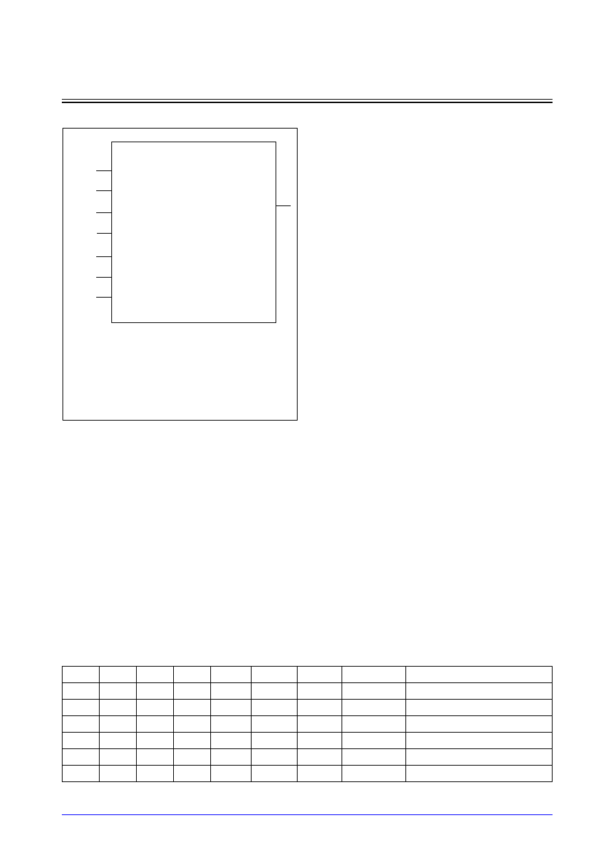
Samsung ASIC
5-39
STDL130
SPSRAMR_HDL
Single-Port Synchronous Static RAM with Redundancy
Logic Symbol
Function Description
SPSRAMR_HDL is a repairable single-port synchronous static RAM with bit-write capability which is
provided as a compiler. SPSRAMR_HDL is intended for use in high-capacity applications. Basically, its
functionality is exactly same as SPSRAMBW_HDL. Each bit of BWEN[] enables or disable the write
operation of its corresponding bit in DI[]. On the rising edge of CK, the write cycle is initiated when WEN is
low and CSN is low. The data bytes or bits in DI[], which their corresponding bit(s) in BWEN[] are low, are
written into the memory location specified on A[]. When all bits of BWEN[] are high, any data in DI[] are not
written into the memory location specified on A[]. When all bits of BWEN[] are low, the data in DI[] are
written into the memory location specified on A[], which is exactly same as the write operation in
SPSRAM_HDL. During the write cycle, DOUT[] remains stable. On the rising edge of CK, the read cycle is
initiated when WEN is high and CSN is low. The data at DOUT[] become valid after a delay. While in standby
mode that CSN is high, A[] and DI[] are disabled, data stored in the memory is retained and DOUT[] remains
stable. When OEN is high, DOUT[] is placed in a high-impedance state.
SPSRAMR_HDL Function Table
CK
CSN
WEN
OEN
A
BWEN
DI
DOUT
Comment
X
X
X
H
X
X
X
Z
Unconditional tri-state output
X
H
X
L
X
X
X
DOUT(t-1)
De-selected (standby mode)
L
L
L
Valid
all L
Valid
DOUT(t-1)
Word-write cycle
L
L
L
Valid
L/H
Valid
DOUT(t-1)
Bit-write cycle
L
L
L
Valid
all H
Valid
DOUT(t-1)
No operation
L
H
L
Valid
X
X
MEM(A)
Read cycle
Features
∑
Suitable for high-capacity application
∑
Heuristic row-redundancy available
∑
Bit-write capability
∑
Separated data I/O
∑
Synchronous operation
∑
Duty-free clock cycle
∑
Asynchronous tri-state output control
∑
Latched inputs and outputs
∑
Automatic power-down
∑
Near zero hold time
∑
Low noise output optimization
∑
Flexible aspect ratio
∑
Dual-bank scheme available
∑
64Kbits ~ 1Mbits capacity
∑
2K ~ 32K number of words
∑
8 ~ 128 number of bits per word
NOTES:
1. Words (w) is the number of words.
2. Bpw (b) is the number of bit per word.
3. Ymux (y) is one of the column mux types.
5. m =
log
2
w
CK
CSN
WEN
spsramr_hdl_<w>x<b>m<y>b<ba>
DOUT [b-1:0]
OEN
A [m-1:0]
DI [b-1:0]
4. Banks(ba) is the number of banks.
BWEN[b-1:0]
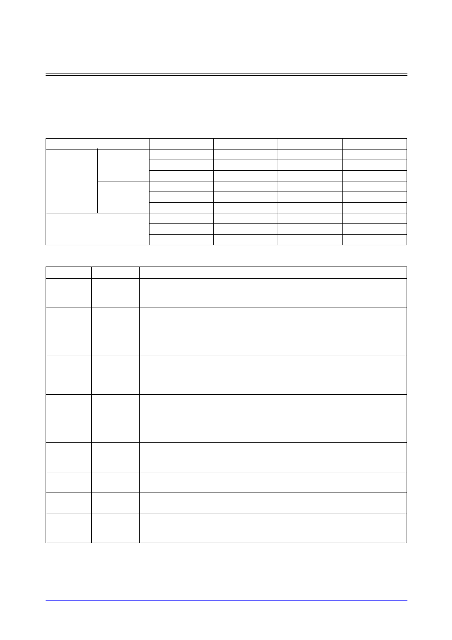
STDL130
5-40
Samsung ASIC
SPSRAMR_HDL
Single-Port Synchronous Static RAM with Redundancy
Parameter Description
SPSRAMR_HDL is the compiler that automatically generates symbol, netlist, timing model, power model
and layout according to the following parameters; Number of words(w), Number of bit per word(b), Column
mux(y) and Number of banks(ba).
Pin Descriptions
Parameters
Ymux(y) = 8
Ymux(y) = 16
Ymux(y) = 32
Words (w)
ba = 1
Min
2048
4096
8192
Max
4096
8192
16384
Step
64
128
256
ba = 2
Min
4096
8192
16384
Max
8192
16384
32768
Step
128
256
512
Bpw (b)
Min
32
16
8
Max
128
64
32
Step
1
1
1
Name
Type
Description
CK
Clock
Clock input. CSN, WEN, A[] and DI[] are latched into the RAM on the rising
edge of CK. If CSN and WEN are low on the rising edge of CK, the RAM is in
write mode. If WEN is high on the rising edge of CK, the RAM is in read mode.
CSN
Chip Enable Chip Enable input. The chip enable is active-low and is latched into the RAM
on the rising edge of CK. When CSN is low, the RAM is enabled for reading or
writing, depending on the state of WEN. When CSN is high, the RAM goes to
the standby mode and is disabled for reading or writing. DOUT remains previ-
ous data output.
WEN
Read/Write
Enable
Read or write enable input. The read/write enable is latched into the RAM on
the rising edge of CK. When WEN is low, data are written to the addressed
location and DOUT remains stable. When WEN is high, data from the
addressed word are present at DOUT.
BWEN[]
Bit-Write
Enable
Bit-write enable input bus. The bit-write enable is latched into the RAM on the
rising edge of CK. Each bit of BWEN[] enables/disables the write operation of
corresponding data bit. BWEN[i] corresponds to DI[i] in bit-write. If WEN and
BWEN[0] are low and BWEN[1] is high, DI[0] is written into the memory loca-
tion specified on A[], but DI[1] is not written.
OEN
Data Output
Enable
Data output enable input. The data output enable is asynchronously operated
regardless of any input. When OEN is high, DOUT is disabled and goes to
high-impedance state.
A[]
Address
Address input bus. The address is latched into the RAM on the rising edge of
CK.
DI[]
Data Input
Data input bus. Data are latched on the rising edge of CK. Data input is writ-
ten into the addressed location in write mode.
DOUT[]
Data Output Data output bus. Data output is valid after the rising edge of CK while the
RAM is in read mode. Data output remains previous data output while the
RAM is in write mode.

Samsung ASIC
5-41
STDL130
SPSRAMR_HDL
Single-Port Synchronous Static RAM with Redundancy
Pin Capacitance
(Unit = SL)
NOTE: Each pin's capacitance is exactly same regardless of available mux types for same bank
Block Diagrams
SPSRAMR_HDL has 2 different physical architectures due to the word depth. Optionally, one of these
architectures is generated from SPSRAMR_HDL compiler. In dual-bank, the bank selected by the address
is only activated while the other bank is in idle mode. In 1-bank architecture, the multi power ports are
located on the middle-edge and the bottom edge of both right- and left-sides of the memory. In 2-bank
architecture, the multi power ports are located on the top-edge, the middle-edge and the bottom-edge of
both right- and left-sides of the memory. All signal ports are only located on the bottom sides of the memory
regardless of architecture.
CK
CSN
WEN
BWEN
OEN
A
DI
DOUT
13.2922
3.1070
3.2305
3.5597
5.2058
3.3539
3.4774
9.4444
<1-bank architecture>
RAM Core
W
ord-line Decoder
X-Dec
W
ord-line Decoder
RAM Core
Y-Dec &
Sense Amp.
Control Block
Y-Dec &
Sense Amp.
I/O Driver
Address &
Clock Buffers
I/O Driver
VDD
VSS
VDD
VSS
VDD
VSS
VDD
VSS
DOUT[b-1:b/2]
DI[b-1:b/2]
A[m-1:0]
WEN
OEN
CSN
CK
DOUT[b/2-1:0]
DI[b/2-1:0]
BWEN[b-1:b/2]
BWEN[b/2-1:0]
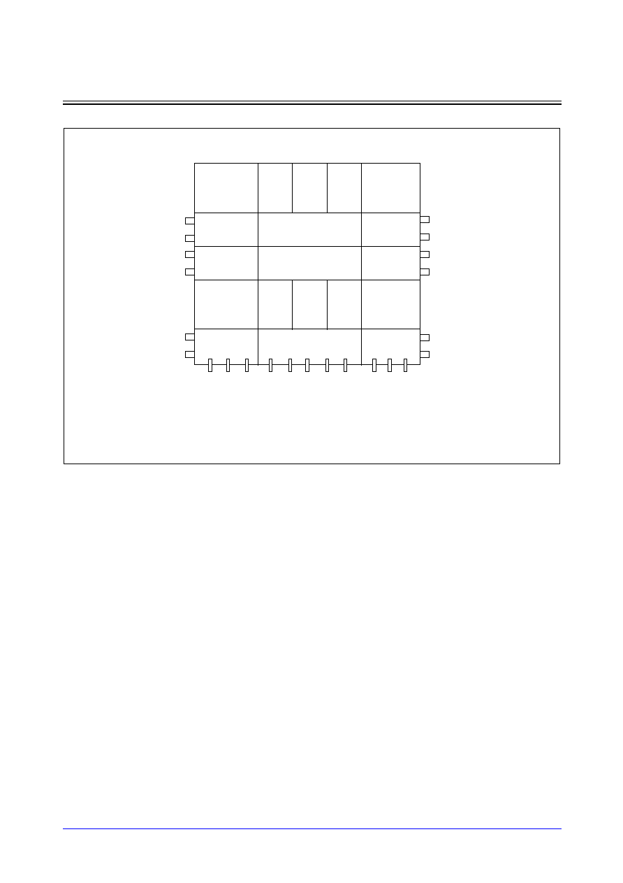
STDL130
5-42
Samsung ASIC
SPSRAMR_HDL
Single-Port Synchronous Static RAM with Redundancy
Application Notes
1.
Permitting over-the-cell routing. In chip-level layout, over-the-cell routing in SPSRAMR_HDL is permitted
for only Metal-5 and Metal-6 layers.
2.
Incoming power bus should be adjusted to guarantee NOT more than 10% voltage drop at typical-case
current levels.
3.
Power stripe should be tapped from both sides of SPSRAMR_HDL.
4.
A byte-write or word-write operation with SPSRAMR_HDL. Refer to the function table. In byte-write
operation, the number of BWEN[] signal bus should be divided by a byte (8) and eight BWEN signals
should be tied to a connection wire. In this case, DI[] bus is controlled by a byte-wired BWEN signal
instead of each BWEN bit. In word-write operation, the functionality is exactly same as SPSRAM_HDL.
If all of BWEN[] signal is tied to low state, DI[] bus is only controlled by WEN.
5.
Power reduction during standby mode. The standby power is measured on the condition that only CSN
is in disable mode and other signals are in operation mode. If any of signals are activated while in standby
mode, the power will be consumed because the input switching activities are occurred by the signal
transition. Therefore, to reduce unnecessary power consumption, you should keep all signals stable
while in standby mode.
<2-bank architecture >
RAM Core
W
ord-line
Decoder
X-Dec
W
ord-line
Decoder
RAM Core
Y-Dec &
Sense Amp.
Control Block
Y-Dec &
Sense Amp.
Y-Dec &
Sense Amp.
Control Block
Y-Dec &
Sense Amp.
RAM Core
W
ord-line
Decoder
X-Dec
W
ord-line
Decoder
RAM Core
I/O Driver
Address &
Clock Buffers
I/O Driver
VSS
VDD
VDD
VSS
VDD
VSS
VSS
VDD
VDD
VSS
VDD
VSS
DOUT[b-1:b/2]
DI[b-1:b/2]
A[m-1:0]
WEN
OEN
CSN
CK
DOUT[b/2-1:0]
DI[b/2-1:0]
BWEN[b-1:b/2]
BWEN[b/2-1:0]

Samsung ASIC
5-43
STDL130
SPSRAMR_HDL
Single-Port Synchronous Static RAM with Redundancy
Characteristics
Definition for AC Timing (ns)
Symbol
Description
Symbol
Description
t
cyc
Clock cycle time
t
ckl
Clock pulse width low
t
ckh
Clock pulse width high
t
as
Address setup time
t
ah
Address hold time
t
cs
CSN setup time
t
ch
CSN hold time
t
ds
Data-In setup time
t
dh
Data-In hold time
t
ws
WEN setup time
t
wh
WEN hold time
t
bws
BWEN setup time
t
bwh
BWEN hold time
t
acc
Data access time
t
da
De-access time
t
dz
DOUT drive to high-Z time
t
zd
DOUT high-Z to drive time
t
od
OEN to valid output time
Definition for Power Consumption (
µ
W/MHz)
Power_read
The dynamic average power consumption while in a read cycle
Power_write
The dynamic average power consumption while in a write cycle
Power_standby
The standby power consumption while CSN is high, OEN is low and other signals are in
normal operations.
Definition for Area (
µ
m)
Width
The physical width in X-direction
Height
The physical height in Y-direction

STDL130
5-44
Samsung ASIC
SPSRAMR_HDL
Single-Port Synchronous Static RAM with Redundancy
Reference Table
* For Ymux=8
(Typical process, 1.8V, 25
∞
C, Output load=10SL, Input slope=0.2 ns, SA=0.5)
NOTE: Standby power is measured on condition that other signals are in normal operation while CSN is in disable
mode.
Parameters
words
2048
4096
2048
4096
04096
8192
4096
8192
bpw
32
32
64
64
64
64
128
128
ba
1
2
1
2
1
2
1
2
Timing (ns)
t
cyc
3.78
3.96
3.84
4.02
4.17
4.53
4.31
4.65
t
ckl
0.58
0.53
0.56
0.53
0.55
0.53
0.57
0.53
t
ckh
0.82
0.82
0.82
0.82
0.82
0.82
0.82
0.83
t
as
0.42
0.42
0.42
0.43
0.42
0.42
0.42
0.41
t
ah
0.17
0.17
0.17
0.17
0.17
0.17
0.17
0.18
t
cs
0.70
0.70
0.70
0.70
0.70
0.70
0.70
0.70
t
ch
0.01
0.01
0.01
0.01
0.01
0.01
0.01
0.01
t
ds
0.22
0.21
0.16
0.17
0.17
0.16
0.08
0.06
t
dh
0.23
0.23
0.32
0.31
0.31
0.32
0.49
0.50
t
ws
0.31
0.35
0.32
0.35
0.32
0.39
0.31
0.39
t
wh
0.24
0.24
0.22
0.22
0.24
0.20
0.24
0.25
t
bws
0.26
0.26
0.21
0.21
0.22
0.21
0.13
0.11
t
bwh
0.25
0.25
0.34
0.34
0.34
0.36
0.53
0.52
t
acc
3.31
3.48
3.38
3.54
3.70
4.01
3.84
4.13
t
da
2.97
3.03
2.99
3.05
3.31
3.44
3.37
3.50
t
dz
0.27
0.27
0.31
0.31
0.31
0.31
0.38
0.38
t
zd
0.37
0.37
0.41
0.41
0.41
0.41
0.48
0.48
t
od
0.56
0.56
0.65
0.64
0.63
0.63
0.82
0.82
Power (
µ
W/MHz)
Power_read
103.40
146.19
175.32
243.91
182.66
255.72
333.53
460.87
Power_write
178.52
231.23
329.56
418.60
435.23
549.83
844.90
1054.60
Power_standby
57.77
92.59
107.23
173.57
107.14
210.35
205.93
408.42
Area (
µ
m)
Width
627.88
627.88
1117.16
1117.16
1117.16
1117.16
2095.72
2095.72
Height
772.90
1494.16
779.30
1506.96
1400.10
2748.56
1425.70
2799.70
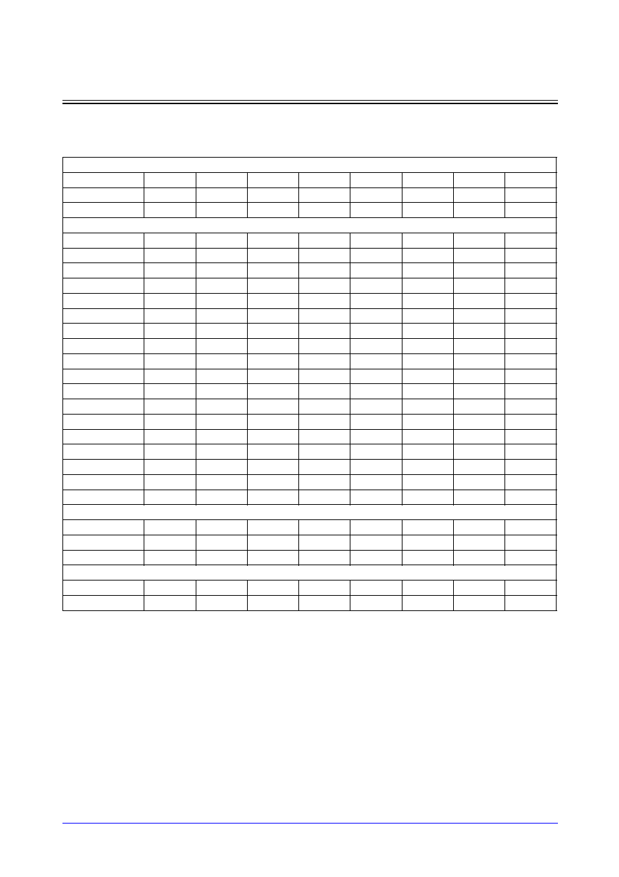
Samsung ASIC
5-45
STDL130
SPSRAMR_HDL
Single-Port Synchronous Static RAM with Redundancy
Reference Table
* For Ymux=16
(Typical process, 1.8V, 25
∞
C, Output load=10SL, Input slope=0.2 ns, SA=0.5)
NOTE: Standby power is measured on condition that other signals are in normal operation while CSN is in disable
mode.
Parameters
words
4096
8192
4096
8192
8192
16384
8192
16384
bpw
16
16
32
32
32
32
64
64
ba
1
2
1
2
1
2
1
2
Timing (ns)
t
cyc
3.81
3.99
3.87
4.05
4.22
4.56
4.35
4.70
t
ckl
0.53
0.53
0.53
0.53
0.53
0.53
0.53
0.53
t
ckh
0.82
0.81
0.82
0.82
0.82
0.82
0.82
0.82
t
as
0.43
0.42
0.43
0.42
0.42
0.42
0.42
0.43
t
ah
0.17
0.16
0.17
0.16
0.17
0.17
0.17
0.17
t
cs
0.70
0.70
0.70
0.70
0.70
0.70
0.70
0.70
t
ch
0.01
0.01
0.01
0.01
0.01
0.01
0.01
0.01
t
ds
0.23
0.22
0.19
0.18
0.19
0.18
0.11
0.11
t
dh
0.21
0.21
0.29
0.28
0.29
0.29
0.43
0.43
t
ws
0.32
0.36
0.32
0.36
0.32
0.39
0.32
0.40
t
wh
0.17
0.24
0.17
0.22
0.22
0.22
0.17
0.17
t
bws
0.27
0.27
0.23
0.23
0.23
0.22
0.15
0.15
t
bwh
0.24
0.24
0.31
0.31
0.32
0.32
0.47
0.47
t
acc
3.33
3.52
3.39
3.58
3.71
4.05
3.84
4.16
t
da
2.95
3.04
2.99
3.07
3.31
3.44
3.38
3.50
t
dz
0.26
0.26
0.29
0.29
0.29
0.29
0.36
0.36
t
zd
0.36
0.36
0.39
0.39
0.39
0.39
0.46
0.46
t
od
0.54
0.54
0.61
0.61
0.62
0.62
0.77
0.77
Power (
µ
W/MHz)
Power_read
125.20
212.71
219.73
377.71
224.43
386.05
417.48
722.38
Power_write
178.76
286.51
329.06
527.94
383.05
596.11
738.40
1144.70
Power_standby
40.03
66.11
71.73
120.35
71.76
138.97
135.30
265.79
Area (
µ
m)
Width
627.88
627.88
1117.16
1117.16
1117.16
1117.16
2095.72
2095.72
Height
772.90
1494.16
779.30
1506.96
1400.10
2748.56
1425.70
2799.70

STDL130
5-46
Samsung ASIC
SPSRAMR_HDL
Single-Port Synchronous Static RAM with Redundancy
Reference Table
* For Ymux=32
(Typical process, 1.8V, 25
∞
C, Output load=10SL, Input slope=0.2 ns, SA=0.5)
NOTE: Standby power is measured on condition that other signals are in normal operation while CSN is in disable
mode.
Parameters
words
8192
16384
8192
16384
16384
32768
16384
32768
bpw
8
8
16
16
16
16
32
32
ba
1
2
1
2
1
2
1
2
Timing (ns)
t
cyc
3.85
4.05
3.91
4.11
4.26
4.63
4.38
4.78
t
ckl
0.53
0.53
0.53
0.53
0.53
0.54
0.53
0.56
t
ckh
0.82
0.82
0.82
0.82
0.82
0.82
0.82
0.83
t
as
0.42
0.42
0.42
0.42
0.42
0.42
0.42
0.42
t
ah
0.17
0.17
0.17
0.17
0.17
0.17
0.17
0.18
t
cs
0.70
0.70
0.70
0.70
0.70
0.70
0.70
0.70
t
ch
0.01
0.01
0.01
0.01
0.01
0.01
0.01
0.01
t
ds
0.24
0.22
0.20
0.19
0.20
0.19
0.13
0.11
t
dh
0.21
0.21
0.27
0.27
0.27
0.27
0.40
0.41
t
ws
0.32
0.35
0.32
0.35
0.32
0.39
0.31
0.38
t
wh
0.24
0.24
0.22
0.24
0.19
0.20
0.24
0.25
t
bws
0.27
0.27
0.24
0.24
0.24
0.24
0.17
0.16
t
bwh
0.23
0.25
0.29
0.31
0.30
0.30
0.42
0.43
t
acc
3.37
3.60
3.44
3.65
3.75
4.12
3.88
4.25
t
da
2.95
3.03
2.99
3.06
3.30
3.45
3.37
3.52
t
dz
0.26
0.26
0.29
0.29
0.29
0.29
0.35
0.35
t
zd
0.36
0.36
0.39
0.39
0.39
0.39
0.44
0.44
t
od
0.53
0.53
0.60
0.60
0.60
0.60
0.73
0.75
Power (
µ
W/MHz)
Power_read
114.10
201.15
197.72
355.38
201.03
362.82
370.96
676.33
Power_write
146.88
249.94
264.42
454.06
292.76
491.06
556.70
933.86
Power_standby
30.83
52.14
53.32
92.63
53.32
102.15
98.34
192.12
Area (
µ
m)
Width
627.88
627.88
1117.16
1117.16
1117.16
1117.16
2095.72
2095.72
Height
772.90
1494.16
779.30
1506.96
1400.10
2748.56
1425.70
2799.70

Samsung ASIC
5-47
STDL130
SPSRAMR_HDL
Single-Port Synchronous Static RAM with Redundancy
Timing Diagrams
Read Cycle
Write Cycle
t
as
A[]
t
ah
(CSN = low, OEN = low, BWEN, DI = don't care)
t
acc
WEN
t
ws
t
wh
t
da
DOUT[]
t
cyc
CK
t
ckl
t
ckh
A0
A2
Valid
M[A0]
M[A1]
M[A2]
A1
t
as
A[]
t
ah
(CSN= low, OEN = don't care)
WEN
t
ws
t
wh
DI[]
t
cyc
CK
t
ckl
t
ckh
A0
A2
BW1
t
ds
t
dh
D0
D2
D1
t
bws
BWEN[]
t
bwh
BW0
BW2
A1

STDL130
5-48
Samsung ASIC
SPSRAMR_HDL
Single-Port Synchronous Static RAM with Redundancy
Read Cycle with CSN-Controlled
OEN-Controlled Output Enable
NOTE: "don't care" means the condition that these pins are in normal operation mode.
t
as
A[]
t
ah
(OEN = low, WEN = high, BWEN, DI = don't care)
CSN
t
cs
t
ch
DOUT[]
t
cyc
CK
t
ckl
t
ckh
A0
A2
A1
t
da
t
acc
M[A1]
M[A0]
(CSN, CK, A, WEN, BWEN, DI = don't care)
t
od
t
dz
Hi-Z
valid
OEN
DOUT[]
Hi-Z
t
zd
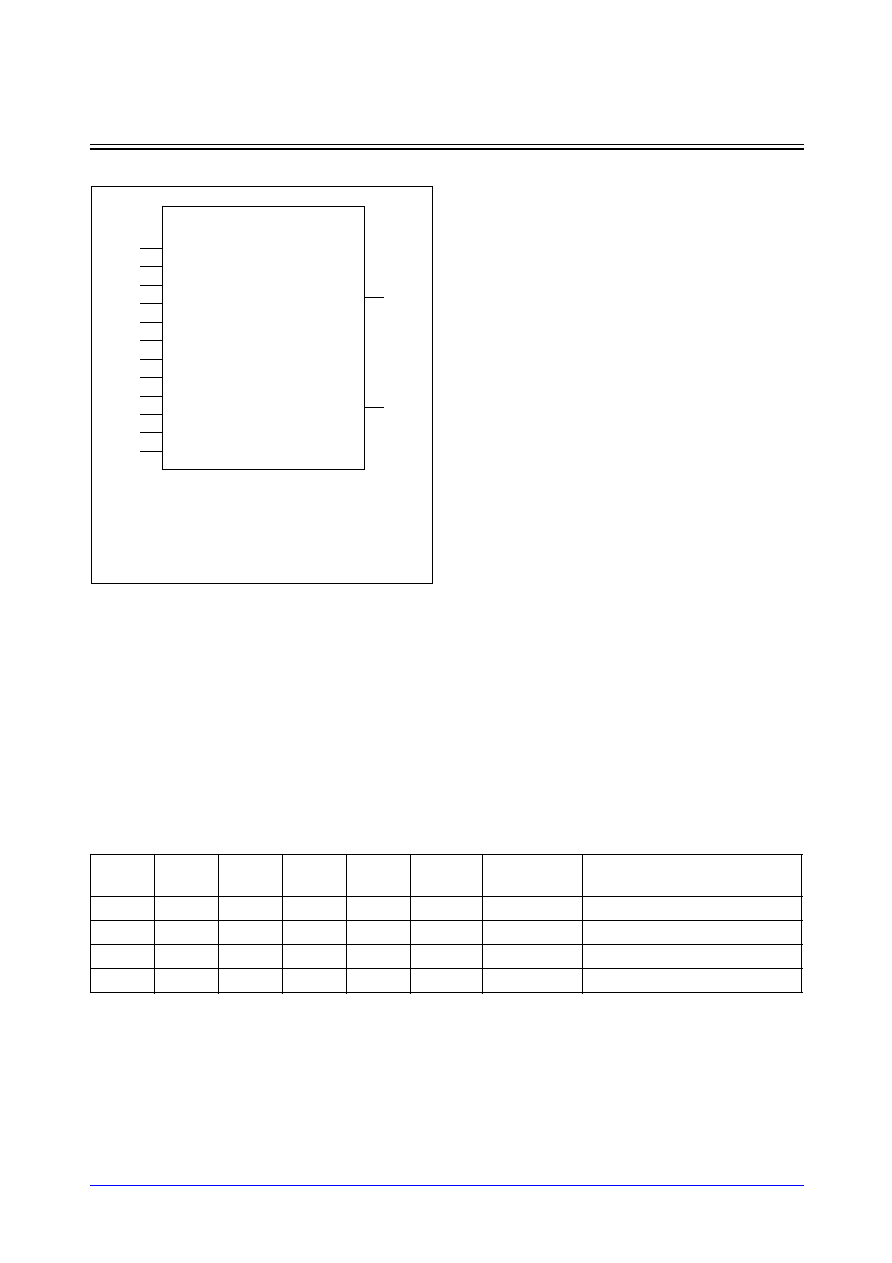
Samsung ASIC
5-49
STDL130
DPSRAM_HDL
High-Density Dual-Port Synchronous Static RAM
Logic Symbol
Function Description
DPSRAM_HDL is a dual-port synchronous static RAM which is provided as a compiler. DPSRAM_HDL is
intended for use in high-density applications. Each port is fully independent. On the rising edge of
CK1(CK2), the write cycle is initiated when WEN1 (WEN2) is low and CSN1 (CSN2) is low. The data on
DI1[] (DI2[]) is written into the memory location specified on A1[](A2[]). During the write cycle, DOUT1[]
(DOUT2[]) remains stable. On the rising edge of CK, the read cycle is initiated when WEN1 (WEN2) is high
and CSN1(CSN2) is low. The data at DOUT1[] (DOUT2[]) become valid after a delay. While in standby mode
that CSN1(CSN2) is high, A1[](A2[]) and DI1[] (DI2[]) are disabled, data stored in the memory is retained
and DOUT1[] (DOUT2[]) remains stable. When OEN1 (OEN2) is high, DOUT1[] (DOUT2[]) is placed in a
high-impedance state.
DPSRAM_HDL Function Table
CK1
CK2
CSN1
CSN2
WEN1
WEN2
OEN1
OEN2
A1
A2
DI1
DI2
DOUT1
DOUT2
Comment
X
X
X
H
X
X
Z
Unconditional tri-state output
X
H
X
L
X
X
DOUT(t-1)
De-selected (standby mode)
L
L
L
Valid
Valid
DOUT(t-1)
Write cycle
L
H
L
Valid
X
MEM(A)
Read cycle
Features
∑
Suitable for high-density application
∑
Separated data I/O
∑
Synchronous operation
∑
Duty-free clock cycle
∑
Asynchronous tri-state output control
∑
Latched inputs and outputs
∑
Automatic power-down
∑
Zero standby current
∑
Zero hold time
∑
Low noise output optimization
∑
Flexible aspect ratio
∑
Up to 256Kbits capacity
∑
Up to 16K number of words
∑
Up to 128 number of bits per word
NOTES:
1. Words (w) is the number of words.
2. Bpw (b) is the number of bits per word.
3. Ymux (y) is one of the column mux types.
4. m =
log
2
w
CK1
CK2
CSN1
CSN2
WEN1
dpsram_hdl_<w>x<b>m<y>
DOUT1 [b-1:0]
WEN2
OEN1
OEN2
A1 [m-1:0]
A2 [m-1:0]
DI1 [b-1:0]
DI2 [b-1:0]
DOUT2 [b-1:0]
STDL130
5-50
Samsung ASIC
DPSRAM_HDL
High-Density Dual-Port Synchronous Static RAM
Parameter Description
DPSRAM_HDL is the compiler that automatically generates symbol, netlist, timing model, power model and
layout according to the following parameters; Number of words(w), Number of bits per word(b) and Column
mux(y).
Pin Descriptions
Pin Capacitance
(Unit = SL)
NOTE: Each pin's capacitance is exactly same regardless of available mux types.
Parameters
Ymux(y) = 4
Ymux(y) = 8
Ymux(y) = 16
Ymux(y) = 32
Words (w)
Min
32
64
128
256
Max
2048
4096
8192
16384
Step
16
32
64
128
Bpw (b)
Min
1
1
1
1
Max
128
64
32
16
Step
1
1
1
1
Name
Type
Description
CK1
CK2
Clock
Clock input. CSN, WEN, A[] and DI[] are latched into the RAM on the rising
edge of CK. If CSN and WEN are low on the rising edge of CK, the RAM is in
write mode. If WEN is high on the rising edge of CK, the RAM is in read mode.
Upon the falling edge of CK, the RAM is in a precharge state.
CSN1
CSN2
Chip Enable Chip enable input. The chip enable is active-low and is latched into the RAM
on the rising edge of CK. When CSN is low, the RAM is enabled for reading or
writing, depending on the state of WEN. When CSN is high, the RAM goes to
the standby mode and is disabled for reading or writing. DOUT remains previ-
ous data output.
WEN1
WEN2
Read/Write
Enable
Read or write enable input. The read/write enable is latched into the RAM on
the rising edge of CK. When WEN is low, data are written to the addressed
location and DOUT remains stable. When WEN is high, data from the
addressed word are presented at DOUT.
OEN1
OEN2
Data Output
Enable
Data output enable input. The data output enable is asynchronously operated
regardless of the state of other inputs. When OEN is high, DOUT is disabled
and goes to high-impedance state.
A1 [ ]
A2 [ ]
Address
Address input bus. The address is latched into the RAM on the rising edge of
CK.
DI1 [ ]
DI2 [ ]
Data Input
Data input bus. Data are latched on the rising edge of CK. Data input is writ-
ten into the addressed location in write mode.
DOUT1 [ ]
DOUT2 [ ]
Data Output Data output bus. Data output is valid after the rising edge of CK while the
RAM is in read mode. Data output remains previous data output while the
RAM is in write mode.
CK
CSN
WEN
OEN
A
DI
DOUT
33.44
4.84
4.84
11.67
4.84
5.49
35.72
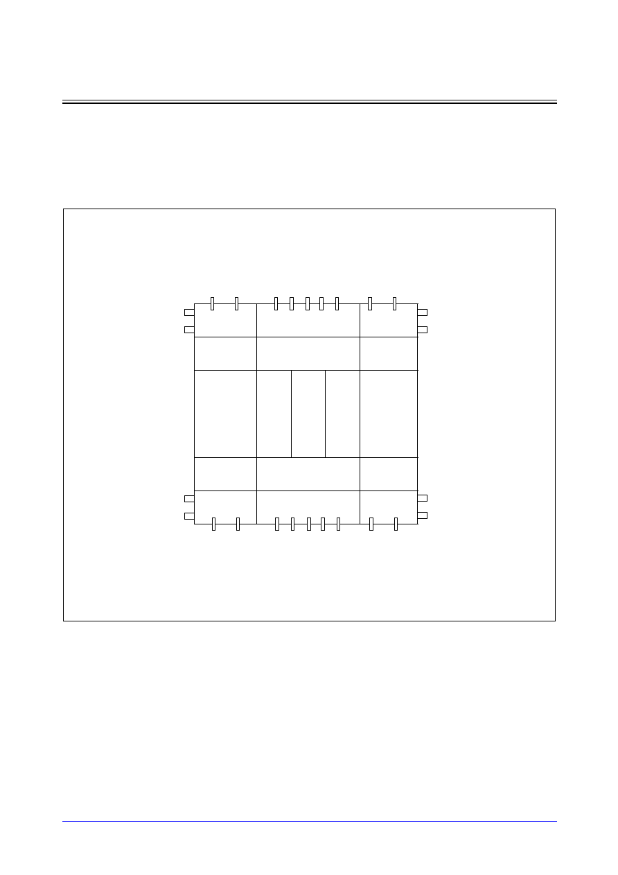
Samsung ASIC
5-51
STDL130
DPSRAM_HDL
High-Density Dual-Port Synchronous Static RAM
Block Diagram
DPSRAM_HDL supports only 1-bank architecture. The power ports are located on the top edge and the
bottom edge of both right- and left-sides of the memory. However, DPSRAM_HDL has two symmetrical
ports located on opposite edges of memory. Port1 is located on the bottom of the memory while Port2 is
located on the top of the memory.
I/O Driver
Address &
Clock Buffers
I/O Driver
Y-Dec &
Sense Amp.
Control Block
Y-Dec &
Sense Amp.
RAM Core
W
ord-line
Decoder
X-Dec
W
ord-line
Decoder
RAM Core
Y-Dec &
Sense Amp.
Control Block
Y-Dec &
Sense Amp.
I/O Driver
Address &
Clock Buffers
I/O Driver
VDD
VSS
DOUT1[b/2-1:0]
DI1[b/2-1:0]
A1[m-1:0]
WEN1
CSN1
CK1
OEN1
DI1[b-1:b/2]
DOUT1[b-1:b/2]
VSS
VDD
VDD
VSS
VSS
VDD
DOUT2[b/2-1:0]
DI2[b/2-1:0]
A2[m-1:0]
WEN2
CSN2
CK2
OEN2
DI2[b-1:b/2]
DOUT2[b-1:b/2]

STDL130
5-52
Samsung ASIC
DPSRAM_HDL
High-Density Dual-Port Synchronous Static RAM
Application Notes
1.
Permitting over-the-cell routing
In chip-level layout, over-the-cell routing in DPSRAM_HDL is permitted for only Metal-5 and Metal-6
layers.
2.
Incoming power bus should be adjusted to guarantee NOT more than 10% voltage drop at typical-case
current levels.
3.
Power stripe should be tapped from both sides of DPSRAM_HDL.
4.
Contention mode in same address access
In DPSRAM_HDL, simultaneous operation by both ports on the same memory address, as write/write,
write/read or read/write operation, causes a contention problem. Simultaneous operation is defined as a
state in which both ports are enabled, both address buses are equal at the rising edge of CK.
DPSRAM_HDL has no scheme preventing the contention. Due to simultaneous operation, silicon will
behave unpredictably. A write operation cannot end and data appearing at outputs may not be valid.
Please refer to the timing diagrams if you want to avoid the contention mode between both ports. In
write/write operation, the data stored at the current address will be unpredictable. In write/read or
read/write operation, the read port is invalid while the write port is still valid. If you want to avoid the
contention mode, you have to give the value greater than tcc (clock-to-clock setup time). However,
simultaneous read/read is allowable without any restrictions.
5.
Power reduction during standby mode.
The standby power is measured on the condition that only CSN is in disable mode and other signals are
in operation mode except that OEN is tied to low. If any of signals are activated while in standby mode,
the power will be consumed because the input switching activities are occurred by the signal transition.
Therefore, to reduce unnecessary power consumption, you should keep stable for all signals while in
standby mode.
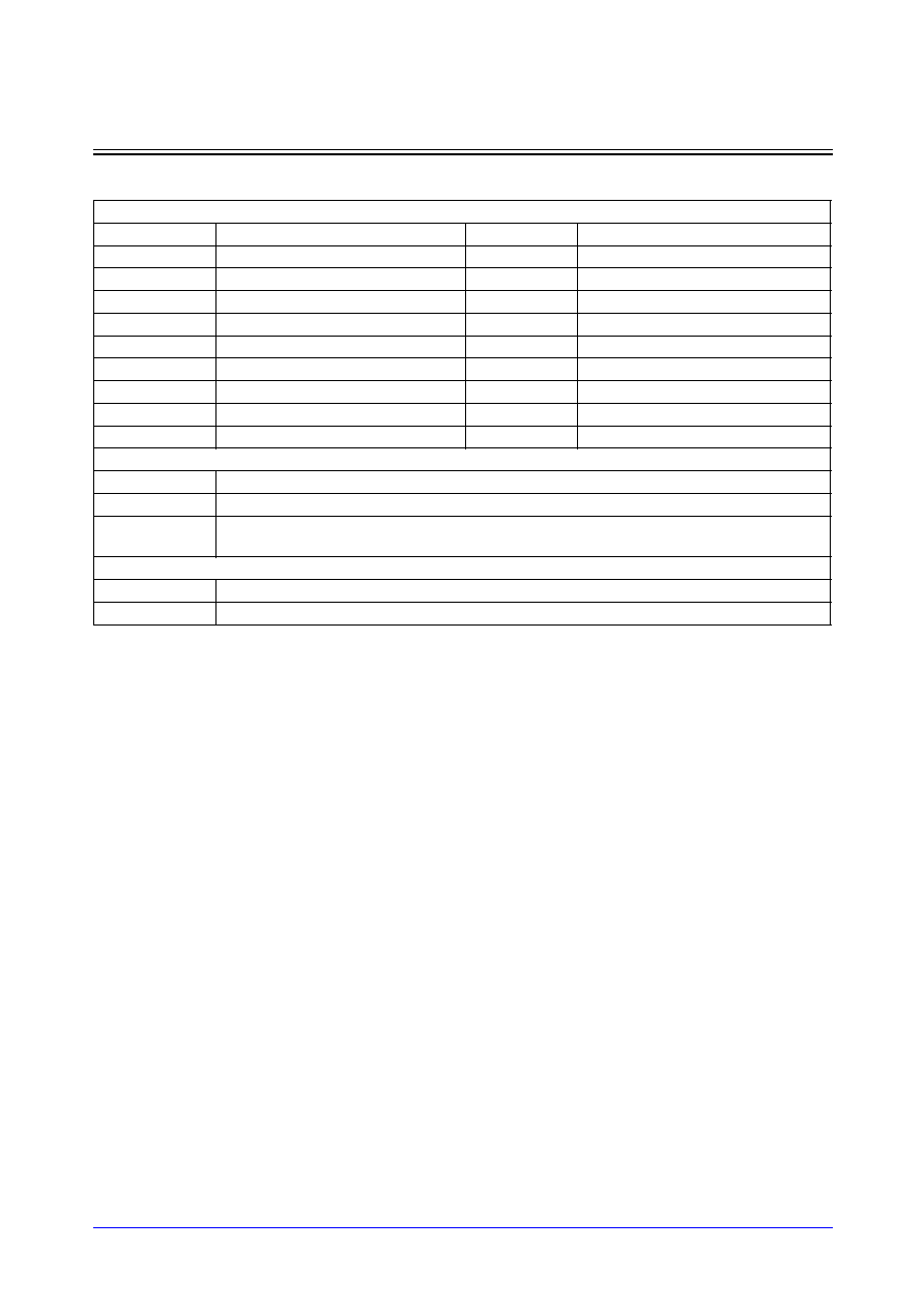
Samsung ASIC
5-53
STDL130
DPSRAM_HDL
High-Density Dual-Port Synchronous Static RAM
Characteristics
Definition for AC Timing (ns)
Symbol
Description
Symbol
Description
t
cyc
Clock cycle time
t
ckl
Clock pulse width low
t
ckh
Clock pulse width high
t
cc
Clock-to-clock setup time
t
as
Address setup time
t
ah
Address hold time
t
cs
CSN setup time
t
ch
CSN hold time
t
ds
Data-In setup time
t
dh
Data-In hold time
t
ws
WEN setup time
t
wh
WEN hold time
t
acc
Data access time
t
da
De-access time
t
dz
DOUT drive to high-Z time
t
zd
DOUT high-Z to drive time
t
od
OEN to valid output time
Definition for Power Consumption (
µ
W/MHz)
Power_read
The dynamic average power consumption while in a read cycle
Power_write
The dynamic average power consumption while in a write cycle
Power_standby
The standby power consumption while CSN is high, OEN is low and other signals are in
normal operations
Definition for Area (
µ
m)
Width
The physical width in X-direction
Height
The physical height in Y-direction

STDL130
5-54
Samsung ASIC
DPSRAM_HDL
High-Density Dual-Port Synchronous Static RAM
Reference Table
* For Ymux=4
(Typical process, 1.8V, 25
∞
C, Output load = 10SL, Input slope = 0.2 ns, SA=0.5)
NOTES:
1.
In power consumption of DPSRAM_HDL, only one port is measured and the other port is isolated.
2.
Standby power is measured on the condition that other signals are in normal operation while CSN is in
disable mode and OEN is low.
Parameters
words
64
128
256
512
768
1024
1536
2048
bpw
16
32
48
64
80
96
112
128
Timing (ns)
t
cyc
2.60
2.67
2.78
2.97
3.11
3.27
3.58
3.63
t
ckl
0.99
0.95
0.92
0.88
0.88
0.85
0.81
0.78
t
ckh
0.42
0.42
0.42
0.42
0.42
0.42
0.42
0.42
t
cc
0.93
1.00
1.10
1.28
1.40
1.58
1.90
1.99
t
as
0.51
0.51
0.51
0.52
0.51
0.50
0.48
0.45
t
ah
0.01
0.01
0.01
0.01
0.01
0.01
0.01
0.01
t
cs
0.56
0.56
0.56
0.56
0.56
0.56
0.56
0.56
t
ch
0.01
0.01
0.01
0.01
0.01
0.01
0.01
0.01
t
ds
0.81
0.77
0.73
0.70
0.69
0.66
0.63
0.60
t
dh
0.01
0.01
0.01
0.01
0.01
0.01
0.01
0.01
t
ws
0.44
0.45
0.46
0.46
0.46
0.47
0.47
0.48
t
wh
0.01
0.01
0.01
0.01
0.01
0.01
0.01
0.01
t
acc
2.32
2.39
2.51
2.69
2.83
2.99
3.30
3.35
t
da
2.19
2.25
2.35
2.53
2.64
2.78
3.05
3.08
t
dz
0.48
0.52
0.56
0.59
0.59
0.62
0.66
0.69
t
zd
0.59
0.61
0.64
0.66
0.68
0.71
0.75
0.79
t
od
0.72
0.76
0.79
0.83
0.84
0.87
0.90
0.93
Power (
µ
W/MHz)
Power_read
85.12
143.24
204.85
274.26
354.25
430.52
526.29
604.69
Power_write
91.14
158.37
232.43
322.29
425.64
530.99
679.63
826.61
Power_standby
30.47
47.91
66.63
87.95
110.35
131.36
157.27
183.05
Area (
µ
m)
Width
551.56
897.16
1242.76
1588.36
2011.96
2357.56
2703.16
3048.76
Height
196.56
220.16
267.36
361.76
454.04
548.30
738.82
927.60

Samsung ASIC
5-55
STDL130
DPSRAM_HDL
High-Density Dual-Port Synchronous Static RAM
Reference Table
* For Ymux=8
(Typical process, 1.8V, 25
∞
C, Output load = 10SL, Input slope = 0.2 ns, SA=0.5)
NOTES:
1.
In power consumption of DPSRAM_HDL, only one port is measured and the other port is isolated.
2.
Standby power is measured on the condition that other signals are in normal operation while CSN is in
disable mode and OEN is low.
Parameters
words
128
256
512
1024
1536
2048
3072
4096
bpw
8
16
24
32
40
48
56
64
Timing (ns)
t
cyc
2.62
2.69
2.81
2.99
3.13
3.30
3.60
3.65
t
ckl
0.99
0.95
0.92
0.88
0.88
0.85
0.52
0.79
t
ckh
0.42
0.42
0.42
0.42
0.42
0.42
0.42
0.42
t
cc
0.93
1.00
1.10
1.28
1.40
1.58
1.90
1.99
t
as
0.51
0.51
0.51
0.52
0.51
0.50
0.48
0.45
t
ah
0.01
0.01
0.01
0.01
0.01
0.01
0.01
0.01
t
cs
0.56
0.56
0.56
0.57
0.56
0.56
0.56
0.56
t
ch
0.01
0.01
0.01
0.01
0.01
0.01
0.01
0.01
t
ds
0.81
0.77
0.74
0.70
0.70
0.67
0.64
0.61
t
dh
0.01
0.01
0.01
0.01
0.01
0.01
0.01
0.01
t
ws
0.44
0.45
0.46
0.46
0.46
0.47
0.47
0.48
t
wh
0.01
0.01
0.01
0.01
0.01
0.01
0.01
0.01
t
acc
2.34
2.42
2.53
2.71
2.85
3.02
3.32
3.37
t
da
2.21
2.27
2.37
2.55
2.66
2.80
3.07
3.10
t
dz
0.48
0.52
0.55
0.59
0.59
0.62
0.65
0.68
t
zd
0.59
0.61
0.64
0.66
0.67
0.71
0.74
0.78
t
od
0.72
0.76
0.79
0.82
0.83
0.87
0.90
0.93
Power (
µ
W/MHz)
Power_read
78.94
130.90
186.34
249.50
322.74
390.88
478.87
549.35
Power_write
77.66
130.73
189.00
259.15
341.26
421.80
533.41
635.85
Power_standby
25.85
38.65
52.75
69.44
88.26
104.91
126.45
148.04
Area (
µ
m)
Width
551.56
897.16
1242.76
1588.36
2011.96
2357.56
2703.16
3048.76
Height
196.56
220.16
267.36
361.76
454.04
548.30
738.82
927.60

STDL130
5-56
Samsung ASIC
DPSRAM_HDL
High-Density Dual-Port Synchronous Static RAM
Reference Table
* For Ymux=16
(Typical process, 1.8V, 25
∞
C, Output load = 10SL, Input slope = 0.2 ns, SA=0.5)
NOTES:
1.
In power consumption of DPSRAM_HDL, only one port is measured and the other port is isolated.
2.
Standby power is measured on the condition that other signals are in normal operation while CSN is in
disable mode and OEN is low.
Parameters
words
256
512
1024
2048
3072
4096
6144
8192
bpw
4
8
12
16
20
24
28
32
Timing (ns)
t
cyc
2.66
2.74
2.85
3.03
3.17
3.34
3.64
3.69
t
ckl
0.99
0.95
0.92
0.89
0.88
0.85
0.82
0.79
t
ckh
0.42
0.42
0.42
0.42
0.42
0.42
0.42
0.42
t
cc
0.93
1.00
1.10
1.28
1.40
1.58
1.90
1.99
t
as
0.51
0.51
0.51
0.52
0.51
0.50
0.48
0.45
t
ah
0.01
0.01
0.01
0.01
0.01
0.01
0.01
0.01
t
cs
0.56
0.56
0.56
0.56
0.56
0.56
0.56
0.56
t
ch
0.01
0.01
0.01
0.01
0.01
0.01
0.01
0.01
t
ds
0.81
0.77
0.74
0.70
0.70
0.67
0.64
0.61
t
dh
0.01
0.01
0.01
0.01
0.01
0.01
0.01
0.01
t
ws
0.44
0.45
0.46
0.46
0.46
0.47
0.47
0.48
t
wh
0.01
0.01
0.01
0.01
0.01
0.01
0.01
0.01
t
acc
2.38
2.46
2.57
2.75
2.89
3.06
3.36
3.41
t
da
2.25
2.32
2.41
2.59
2.70
2.84
3.11
3.14
t
dz
0.48
0.52
0.55
0.59
0.59
0.62
0.65
0.68
t
zd
0.59
0.62
0.64
0.66
0.67
0.71
0.74
0.78
t
od
0.72
0.75
0.79
0.82
0.83
0.86
0.89
0.92
Power (
µ
W/MHz)
Power_read
76.55
124.80
176.52
235.95
306.04
370.88
455.52
522.06
Power_write
71.82
116.86
166.27
225.58
296.70
364.14
457.15
536.50
Power_standby
23.63
33.56
44.78
64.01
74.97
88.83
107.67
126.50
Area (
µ
m)
Width
551.56
897.16
1242.76
1588.36
2011.96
2357.56
2703.16
3048.76
Height
196.56
220.16
267.36
361.76
454.04
548.30
738.82
927.60

Samsung ASIC
5-57
STDL130
DPSRAM_HDL
High-Density Dual-Port Synchronous Static RAM
Reference Table
* For Ymux=32
(Typical process, 1.8V, 25
∞
C, Output load = 10SL, Input slope = 0.2 ns, SA=0.5)
NOTES:
1.
In power consumption of DPSRAM_HDL, only one port is measured and the other port is isolated.
2.
Standby power is measured on the condition that other signals are in normal operation while CSN is in
disable mode and OEN is low.
Parameters
words
512
1024
2048
4096
6144
8192
12288
16384
bpw
2
4
6
8
10
12
14
16
Timing (ns)
t
cyc
2.74
2.81
2.92
3.11
3.25
3.42
3.72
3.77
t
ckl
0.99
0.96
0.92
0.89
0.88
0.86
0.84
0.82
t
ckh
0.42
0.42
0.42
0.42
0.42
0.42
0.42
0.42
t
cc
0.92
0.99
1.10
1.28
1.41
1.58
1.90
1.99
t
as
0.51
0.51
0.51
0.52
0.51
0.50
0.48
0.45
t
ah
0.01
0.01
0.01
0.01
0.01
0.01
0.01
0.01
t
cs
0.56
0.56
0.56
0.56
0.56
0.56
0.56
0.56
t
ch
0.01
0.01
0.01
0.01
0.01
0.01
0.01
0.01
t
ds
0.81
0.77
0.74
0.70
0.69
0.68
0.66
0.64
t
dh
0.01
0.01
0.01
0.01
0.01
0.01
0.01
0.01
t
ws
0.44
0.45
0.46
0.46
0.46
0.47
0.48
0.48
t
wh
0.01
0.01
0.01
0.01
0.01
0.01
0.01
0.01
t
acc
2.45
2.53
2.64
2.83
2.97
3.14
3.44
3.49
t
da
2.33
2.39
2.49
2.66
2.77
2.91
3.18
3.21
t
dz
0.48
0.52
0.55
0.59
0.60
0.62
0.65
0.68
t
zd
0.60
0.62
0.64
0.66
0.66
0.70
0.74
0.78
t
od
0.72
0.75
0.79
0.82
0.84
0.87
0.89
0.92
Power (
µ
W/MHz)
Power_read
76.14
122.30
171.91
229.17
298.21
361.04
443.86
508.62
Power_write
70.22
110.68
155.18
208.77
274.68
335.43
418.81
486.29
Power_standby
22.75
31.11
40.76
53.00
68.33
80.78
98.25
115.73
Area (
µ
m)
Width
551.56
897.16
1242.76
1588.36
2011.96
2357.56
2703.16
3048.76
Height
196.56
220.16
267.36
361.76
454.04
548.30
738.82
927.60
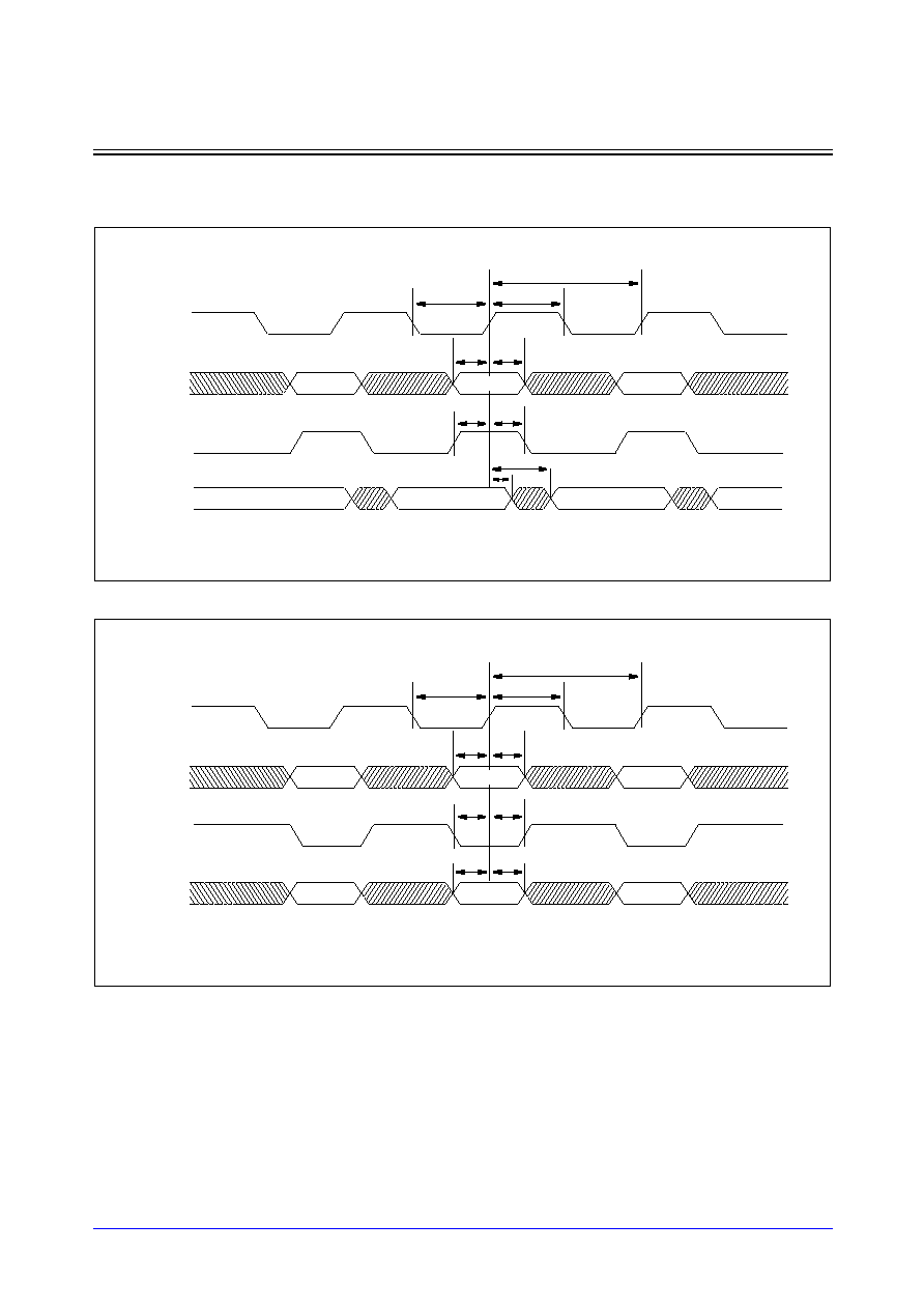
STDL130
5-58
Samsung ASIC
DPSRAM_HDL
High-Density Dual-Port Synchronous Static RAM
Timing Diagrams
Read Cycle
Write Cycle
t
as
A[]
t
ah
(CSN = low, OEN = low, DI[] = don't care)
t
acc
WEN
t
ws
t
wh
t
da
DOUT[]
t
cyc
CK
t
ckl
t
ckh
A0
A2
Valid
M[A0]
M[A1]
M[A2]
A1
t
as
A[]
t
ah
(CSN= low, OEN = don't care)
WEN
t
ws
t
wh
DI[]
t
cyc
CK
t
ckl
t
ckh
A0
A2
A1
t
ds
t
dh
D0
D2
D1

Samsung ASIC
5-59
STDL130
DPSRAM_HDL
High-Density Dual-Port Synchronous Static RAM
Read Cycle with CSN-Controlled
OEN-Controlled Output Enable
Contention Mode
NOTE: "don't care" means the condition that these pins are in normal operation mode.
t
as
A[]
t
ah
(OEN = low, WEN = high, DI[] = don't care)
CSN
t
cs
t
ch
DOUT[]
t
cyc
CK
t
ckl
t
ckh
A0
A2
A1
t
da
t
acc
M[A1]
M[A0]
(CSN, CK, A[], WEN, DI[] = don't care)
t
od
t
dz
Hi-Z
VALID
OEN
DOUT[]
Hi-Z
t
zd
CK1
tcc
CK2
(A1[] = A2[])

STDL130
5-60
Samsung ASIC
DPSRAMBW_HDL
High-Density Dual-Port Synchronous Static RAM with Bit-Write
Logic Symbol
Function Description
DPSRAMBW_HDL is a dual-port synchronous static RAM with bit-write capability which is provided as a
compiler. DPSRAMBW_HDL is intended for use in high-density applications. Each port is fully independent.
Basically, its functionality is exactly same as DPSRAM_HDL except a bit-write operation which is controlled
by BWEN1[](BWEN2[]), named bit-write enable signal bus. Each bit of BWEN1[](BWEN2[]) enables or
disable the write operation of its corresponding bit in DI1[](DI2[]). On the rising edge of CK1(CK2), the write
cycle is initiated when WEN1(WEN2) is low and CSN1(CSN2) is low. The data bits in DI1[](DI2[]), which
their corresponding bit(s) in BWEN1[](BWEN2[]) are low, are written into the memory location specified on
A1[](A2[]). When all bits of BWEN1[](BWEN2[]) are high, any data in DI1[](DI2[]) are not written into the
memory location specified on A1[](A2[]). When all bits of BWEN1[](BWEM2[]) are low, the data in
DI1[](DI2[]) are written into the memory location specified on A1[](A2[]), which is exactly same as the write
operation in DPSRAMBW_HDL. During the write cycle, DOUT1[](DOUT2[]) remains stable. On the rising
edge of CK1(CK2), the read cycle is initiated when WEN1(WEN2) is high and CSN1(CSN2) is low. The data
at DOUT1[](DOUT2[]) become valid after a delay. While in standby mode that CSN1(CSN2) is high,
A1[](A2[]) and DI1[](DI2[]) are disabled, data stored in the memory is retained and DOUT1[](DOUT2[])
remains stable. When OEN1(OEN2) is high, DOUT1[](DOUT2[]) is placed in a high-impedance state.
DPSRAMBW_HDL Function Table
CK1
CK2
CSN1
CSN2
WEN1
WEN2
OEN1
OEN2
A1
A2
BWEN1
BWEN2
DI1
DI2
DOUT1
DOUT2
Comment
X
X
X
H
X
X
X
Z
Unconditional tri-state output
X
H
X
L
X
X
X
DOUT(t-1)
De-selected (standby mode)
L
L
L
Valid
All L
Valid
DOUT(t-1)
Word-write cycle
L
L
L
Valid
L
Valid
DOUT(t-1)
Bit-write cycle
L
L
L
Valid
All H
Valid
DOUT(t-1)
No operation
L
H
L
Valid
X
X
MEM(A)
Read cycle
Features
∑
Suitable for high-density application
∑
Separated data I/O
∑
Synchronous operation
∑
Duty-free clock cycle
∑
Asynchronous tri-state output control
∑
Latched inputs and outputs
∑
Automatic power-down
∑
Automatic power-down
∑
Zero standby current
∑
Zero hold time
∑
Low noise output optimization
∑
Flexible aspect ratio
∑
Up to 256Kbits capacity
∑
Up to 16K number of words
∑
Up to 128 number of bits per word
2. Bpw (b) is the number of bits per word.
3. Ymux (y) is one of the column mux types.
4. m =
log
2
w
CK1
CK2
CSN1
CSN2
WEN1
dpsrambw_hdl_<w>x<b>m<y>
DOUT1 [b-1:0]
WEN2
OEN1
OEN2
A1 [m-1:0]
A2 [m-1:0]
DI1 [b-1:0]
DI2 [b-1:0]
DOUT2 [b-1:0]
NOTES:
1. Words (w) is the number of words.
BWEN1[b-1:0]
BWEN2[b-1:0]
Samsung ASIC
5-61
STDL130
DPSRAMBW_HDL
High-Density Dual-Port Synchronous Static RAM with Bit-Write
Parameter Description
DPSRAMBW_HDL is the compiler that automatically generates symbol, netlist, timing model, power model
and layout according to the following parameters; Number of words(w), Number of bits per word(b) and
Column mux(y).
Pin Descriptions
Pin Capacitance
(Unit = SL)
NOTE: Each pin's capacitance is exactly same regardless of available mux types.
Parameters
Ymux(y) = 4
Ymux(y) = 8
Ymux(y) = 16
Ymux(y) = 32
Words (w)
Min
32
64
128
256
Max
2048
4096
8192
16384
Step
16
32
64
128
Bpw (b)
Min
1
1
1
1
Max
128
64
32
16
Step
1
1
1
1
Name
Type
Description
CK1
CK2
Clock
Clock input. CSN, WEN, A[] and DI[] are latched into the RAM on the rising
edge of CK. If CSN and WEN are low on the rising edge of CK, the RAM is in
write mode. If WEN is high on the rising edge of CK, the RAM is in read mode.
Upon the falling edge of CK, the RAM is in a precharge state.
CSN1
CSN2
Chip Enable Chip enable input. The chip enable is active-low and is latched into the RAM
on the rising edge of CK. When CSN is low, the RAM is enabled for reading or
writing, depending on the state of WEN. When CSN is high, the RAM goes to
the standby mode and is disabled for reading or writing. DOUT remains previ-
ous data output.
WEN1
WEN2
Read/Write
Enable
Read or write enable input. The read/write enable is latched into the RAM on
the rising edge of CK. When WEN is low, data are written to the addressed
location and DOUT remains stable. When WEN is high, data from the
addressed word are presented at DOUT.
BWEN1[ ]
BWEN2[ ]
Bit-Write
Enable
Bit-write enable input bus. The bit-write enable is latched into the RAM on the
rising edge of CK. Each bit of BWEN[] enables/disables the write operation of
corresponding data bit. BWEN[i] corresponds to DI[i] in bit-write. If WEN and
BWEN[0] are low and BWEN[1] is high, DI[0] is written into the memory loca-
tion specified on A[], but DI[1] is not written.
OEN1
OEN2
Data Output
Enable
Data output enable input. The data output enable is asynchronously operated
regardless of the state of other inputs. When OEN is high, DOUT is disabled
and goes to high-impedance state.
A1 [ ]
A2 [ ]
Address
Address input bus. The address is latched into the RAM on the rising edge of
CK.
DI1 [ ]
DI2 [ ]
Data Input
Data input bus. Data are latched on the rising edge of CK. Data input is writ-
ten into the addressed location in write mode.
DOUT1 [ ]
DOUT2 [ ]
Data Output Data output bus. Data output is valid after the rising edge of CK while the
RAM is in read mode. Data output remains previous data output while the
RAM is in write mode.
CK
CSN
WEN
OEN
A
BWEN
DI
DOUT
33.44
4.84
4.84
11.67
4.84
5.49
5.49
35.72

STDL130
5-62
Samsung ASIC
DPSRAMBW_HDL
High-Density Dual-Port Synchronous Static RAM Bit-Write
Block Diagram
DPSRAMBW_HDL supports only 1-bank architecture. The power ports are located on the top edge and the
bottom edge of both right- and left-sides of the memory. However, DPSRAMBW_HDL has two symmetrical
ports located on opposite edges of memory. Port1 is located on the bottom of the memory while Port2 is
located on the top of the memory.
I/O Driver
Address &
Clock Buffers
I/O Driver
Y-Dec &
Sense Amp.
Control Block
Y-Dec &
Sense Amp.
RAM Core
W
ord-line
Decoder
X-Dec
W
ord-line
Decoder
RAM Core
Y-Dec &
Sense Amp.
Control Block
Y-Dec &
Sense Amp.
I/O Driver
Address &
Clock Buffers
I/O Driver
VDD
VSS
DOUT1[b/2-1:0]
DI1[b/2-1:0]
A1[m-1:0]
WEN1
CSN1
CK1
OEN1
DI1[b-1:b/2]
DOUT1[b-1:b/2]
VSS
VDD
VDD
VSS
VSS
VDD
DOUT2[b/2-1:0]
DI2[b/2-1:0]
A2[m-1:0]
WEN2
CSN2
CK2
OEN2
DI2[b-1:b/2]
DOUT2[b-1:b/2]
BWEN2[b-1:b/2]
BWEN2[b/2-1:0]
BWEN1[b-1:b/2]
BWEN1[b/2-1:0]

Samsung ASIC
5-63
STDL130
DPSRAMBW_HDL
High-Density Dual-Port Synchronous Static RAM with Bit-Write
Application Notes
1.
Permitting over-the-cell routing
In chip-level layout, over-the-cell routing in DPSRAMBW_HDL is permitted for only Metal-5 and Metal-6
layers.
2.
Incoming power bus should be adjusted to guarantee NOT more than 10% voltage drop at typical-case
current levels.
3.
Power stripe should be tapped from both sides of DPSRAMBW_HDL.
4.
Contention mode in same address access
In DPSRAMBW_HDL, simultaneous operation by both ports on the same memory address, as
write/write, write/read or read/write operation, causes a contention problem. Simultaneous operation is
defined as a state in which both ports are enabled, both address buses are equal at the rising edge of
CK. DPSRAMBW_HDL has no scheme preventing the contention. Due to simultaneous operation,
silicon will behave unpredictably. A write operation cannot end and data appearing at outputs may not
be valid. Please refer to the timing diagrams if you want to avoid the contention mode between both
ports. In write/write operation, the data stored at the current address will be unpredictable. In write/read
or read/write operation, the read port is invalid while the write port is still valid. If you want to avoid the
contention mode, you have to give the value greater than tcc (clock-to-clock setup time). However,
simultaneous read/read is allowable without any restrictions.
5.
A byte-write or word-write operation with DPSRAMBW_HDL
Refer to the function table. In byte-write operation, the number of BWEN[] signal bus should be divided
by a byte (8) and eight BWEN signals should be tied to a connection wire. In this case, DI[] bus is
controlled by a byte-wired BWEN signal instead of each BWEN bit. In word-write operation, the
functionality is exactly same as DPSRAM_HDL. If all of BWEN[] signal is tied to low state, DI[] bus is
only controlled by WEN.
6.
Power reduction during standby mode.
The standby power is measured on the condition that only CSN is in disable mode and other signals are
in operation mode except that OEN is tied to low. If any of signals are activated while in standby mode,
the power will be consumed because the input switching activities are occurred by the signal transition.
Therefore, to reduce unnecessary power consumption, you should keep stable for all signals while in
standby mode.
STDL130
5-64
Samsung ASIC
DPSRAMBW_HDL
High-Density Dual-Port Synchronous Static RAM with Bit-Write
Characteristics
Definition for AC Timing (ns)
Symbol
Description
Symbol
Description
t
cyc
Clock cycle time
t
ckl
Clock pulse width low
t
ckh
Clock pulse width high
t
cc
Clock-to-clock setup time
t
as
Address setup time
t
ah
Address hold time
t
cs
CSN setup time
t
ch
CSN hold time
t
ds
Data-In setup time
t
dh
Data-In hold time
t
ws
WEN setup time
t
wh
WEN hold time
t
bws
BWEN setup time
t
bwh
BWEN hold time
t
acc
Data access time
t
da
De-access time
t
dz
DOUT drive to high-Z time
t
zd
DOUT high-Z to drive time
t
od
OEN to valid output time
Definition for Power Consumption (
µ
W/MHz)
Power_read
The dynamic average power consumption while in a read cycle
Power_write
The dynamic average power consumption while in a write cycle
Power_standby
The standby power consumption while CSN is high, OEN is low and other signals are in
normal operations.
Definition for Area (
µ
m)
Width
The physical width in X-direction
Height
The physical height in Y-direction

Samsung ASIC
5-65
STDL130
DPSRAMBW_HDL
High-Density Dual-Port Synchronous Static RAM with Bit-Write
Reference Table
* For Ymux=4
(Typical process, 1.8V, 25
∞
C, Output load = 10SL, Input slope = 0.2 ns, SA=0.5)
NOTES:
1.
In power consumption of DPSRAMBW_HDL, only one port is measured and the other port is isolated.
2.
Standby power is measured on the condition that other signals are in normal operation while CSN is in
disable mode and OEN is low.
Parameters
words
64
128
256
512
768
1024
1536
2048
bpw
16
32
48
64
80
96
112
128
Timing (ns)
t
cyc
2.60
2.67
2.78
2.97
3.11
3.27
3.58
3.63
t
ckl
0.99
0.95
0.92
0.88
0.88
0.85
0.81
0.78
t
ckh
0.42
0.42
0.42
0.42
0.42
0.42
0.42
0.42
t
cc
0.93
1.00
1.10
1.28
1.40
1.58
1.90
1.99
t
as
0.51
0.51
0.51
0.52
0.51
0.50
0.48
0.45
t
ah
0.01
0.01
0.01
0.01
0.01
0.01
0.01
0.01
t
cs
0.56
0.56
0.56
0.56
0.56
0.56
0.56
0.56
t
ch
0.01
0.01
0.01
0.01
0.01
0.01
0.01
0.01
t
ds
0.81
0.77
0.73
0.70
0.69
0.66
0.63
0.60
t
dh
0.01
0.01
0.01
0.01
0.01
0.01
0.01
0.01
t
ws
0.44
0.45
0.46
0.46
0.46
0.47
0.47
0.48
t
wh
0.01
0.01
0.01
0.01
0.01
0.01
0.01
0.01
t
bws
0.77
0.74
0.70
0.66
0.66
0.63
0.59
0.56
t
bwh
0.01
0.01
0.01
0.01
0.01
0.01
0.01
0.01
t
acc
2.32
2.39
2.51
2.69
2.83
2.99
3.30
3.35
t
da
2.19
2.25
2.35
2.53
2.64
2.78
3.05
3.08
t
dz
0.48
0.52
0.56
0.59
0.59
0.62
0.66
0.69
t
zd
0.59
0.61
0.64
0.66
0.68
0.71
0.75
0.79
t
od
0.72
0.76
0.79
0.83
0.84
0.87
0.90
0.93
Power (
µ
W/MHz)
Power_read
89.07
151.14
216.71
290.07
373.98
454.24
553.97
636.24
Power_write
95.09
166.27
244.29
338.10
445.38
554.71
707.31
858.16
Power_standby
34.42
55.81
78.49
103.76
130.08
155.07
184.95
214.60
Area (
µ
m)
Width
551.56
897.16
1242.76
1588.36
2011.96
2357.56
2703.16
3048.76
Height
196.56
220.16
267.36
361.76
454.04
548.30
738.82
927.60

STDL130
5-66
Samsung ASIC
DPSRAMBW_HDL
High-Density Dual-Port Synchronous Static RAM with Bit-Write
Reference Table
* For Ymux=8
(Typical process, 1.8V, 25
∞
C, Output load = 10SL, Input slope = 0.2 ns, SA=0.5)
NOTES:
1.
In power consumption of DPSRAMBW_HDL, only one port is measured and the other port is isolated.
2.
Standby power is measured on the condition that other signals are in normal operation while CSN is in
disable mode and OEN is low.
Parameters
words
128
256
512
1024
1536
2048
3072
4096
bpw
8
16
24
32
40
48
56
64
Timing (ns)
t
cyc
2.62
2.69
2.81
2.99
3.13
3.30
3.60
3.65
t
ckl
0.99
0.95
0.92
0.88
0.88
0.85
0.52
0.79
t
ckh
0.42
0.42
0.42
0.42
0.42
0.42
0.42
0.42
t
cc
0.93
1.00
1.10
1.28
1.40
1.58
1.90
1.99
t
as
0.51
0.51
0.51
0.52
0.51
0.50
0.48
0.45
t
ah
0.01
0.01
0.01
0.01
0.01
0.01
0.01
0.01
t
cs
0.56
0.56
0.56
0.57
0.56
0.56
0.56
0.56
t
ch
0.01
0.01
0.01
0.01
0.01
0.01
0.01
0.01
t
ds
0.81
0.77
0.74
0.70
0.70
0.67
0.64
0.61
t
dh
0.01
0.01
0.01
0.01
0.01
0.01
0.01
0.01
t
ws
0.44
0.45
0.46
0.46
0.46
0.47
0.47
0.48
t
wh
0.01
0.01
0.01
0.01
0.01
0.01
0.01
0.01
t
bws
0.78
0.74
0.70
0.66
0.66
0.63
0.60
0.57
t
bwh
0.01
0.01
0.01
0.01
0.01
0.01
0.01
0.01
t
acc
2.34
2.42
2.53
2.71
2.85
3.02
3.32
3.37
t
da
2.21
2.27
2.37
2.55
2.66
2.80
3.07
3.10
t
dz
0.48
0.52
0.55
0.59
0.59
0.62
0.65
0.68
t
zd
0.59
0.61
0.64
0.66
0.67
0.71
0.74
0.78
t
od
0.72
0.76
0.79
0.82
0.83
0.87
0.90
0.93
Power (
µ
W/MHz)
Power_read
80.92
134.86
192.27
257.42
332.62
402.73
492.70
565.13
Power_write
79.63
134.68
194.93
267.07
351.14
433.65
547.23
651.63
Power_standby
27.82
42.60
58.68
77.35
98.14
116.76
140.27
163.82
Area (
µ
m)
Width
551.56
897.16
1242.76
1588.36
2011.96
2357.56
2703.16
3048.76
Height
196.56
220.16
267.36
361.76
454.04
548.30
738.82
927.60
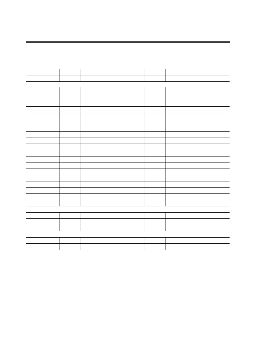
Samsung ASIC
5-67
STDL130
DPSRAMBW_HDL
High-Density Dual-Port Synchronous Static RAM with Bit-Write
Reference Table
* For Ymux=16
(Typical process, 1.8V, 25
∞
C, Output load = 10SL, Input slope = 0.2 ns, SA=0.5)
NOTES:
1.
In power consumption of DPSRAMBW_HDL, only one port is measured and the other port is isolated.
2.
Standby power is measured on the condition that other signals are in normal operation while CSN is in
disable mode and OEN is low.
Parameters
words
256
512
1024
2048
3072
4096
6144
8192
bpw
4
8
12
16
20
24
28
32
Timing (ns)
t
cyc
2.66
2.74
2.85
3.03
3.17
3.34
3.64
3.69
t
ckl
0.99
0.95
0.92
0.89
0.88
0.85
0.82
0.79
t
ckh
0.42
0.42
0.42
0.42
0.42
0.42
0.42
0.42
t
cc
0.93
1.00
1.10
1.28
1.40
1.58
1.90
1.99
t
as
0.51
0.51
0.51
0.52
0.51
0.50
0.48
0.45
t
ah
0.01
0.01
0.01
0.01
0.01
0.01
0.01
0.01
t
cs
0.56
0.56
0.56
0.56
0.56
0.56
0.56
0.56
t
ch
0.01
0.01
0.01
0.01
0.01
0.01
0.01
0.01
t
ds
0.81
0.77
0.74
0.70
0.70
0.67
0.64
0.61
t
dh
0.01
0.01
0.01
0.01
0.01
0.01
0.01
0.01
t
ws
0.44
0.45
0.46
0.46
0.46
0.47
0.47
0.48
t
wh
0.01
0.01
0.01
0.01
0.01
0.01
0.01
0.01
t
bws
0.78
0.74
0.70
0.67
0.66
0.63
0.60
0.57
t
bwh
0.01
0.01
0.01
0.01
0.01
0.01
0.01
0.01
t
acc
2.38
2.46
2.57
2.75
2.89
3.06
3.36
3.41
t
da
2.25
2.32
2.41
2.59
2.70
2.84
3.11
3.14
t
dz
0.48
0.52
0.55
0.59
0.59
0.62
0.65
0.68
t
zd
0.59
0.62
0.64
0.66
0.67
0.71
0.74
0.78
t
od
0.72
0.75
0.79
0.82
0.83
0.86
0.89
0.92
Power (
µ
W/MHz)
Power_read
77.53
126.78
179.48
239.90
310.98
376.81
462.42
529.95
Power_write
72.81
118.83
169.23
229.53
301.65
370.06
464.05
544.39
Power_standby
24.62
35.53
47.74
62.54
79.91
94.75
114.57
134.39
Area (
µ
m)
Width
551.56
897.16
1242.76
1588.36
2011.96
2357.56
2703.16
3048.76
Height
196.56
220.16
267.36
361.76
454.04
548.30
738.82
927.60

STDL130
5-68
Samsung ASIC
DPSRAMBW_HDL
High-Density Dual-Port Synchronous Static RAM with Bit-Write
Reference Table
* For Ymux=32
(Typical process, 1.8V, 25
∞
C, Output load = 10SL, Input slope = 0.2 ns, SA=0.5)
NOTES:
1.
In power consumption of DPSRAMBW_HDL, only one port is measured and the other port is isolated.
2.
Standby power is measured on the condition that other signals are in normal operation while CSN is in
disable mode and OEN is low.
Parameters
words
512
1024
2048
4096
6144
8192
12288
16384
bpw
2
4
6
8
10
12
14
16
Timing (ns)
t
cyc
2.74
2.81
2.92
3.11
3.25
3.42
3.72
3.77
t
ckl
0.99
0.96
0.92
0.89
0.88
0.86
0.84
0.82
t
ckh
0.42
0.42
0.42
0.42
0.42
0.42
0.42
0.42
t
cc
0.92
0.99
1.10
1.28
1.41
1.58
1.90
1.99
t
as
0.51
0.51
0.51
0.52
0.51
0.50
0.48
0.45
t
ah
0.01
0.01
0.01
0.01
0.01
0.01
0.01
0.01
t
cs
0.56
0.56
0.56
0.56
0.56
0.56
0.56
0.56
t
ch
0.01
0.01
0.01
0.01
0.01
0.01
0.01
0.01
t
ds
0.81
0.77
0.74
0.70
0.69
0.68
0.66
0.64
t
dh
0.01
0.01
0.01
0.01
0.01
0.01
0.01
0.01
t
ws
0.44
0.45
0.46
0.46
0.46
0.47
0.48
0.48
t
wh
0.01
0.01
0.01
0.01
0.01
0.01
0.01
0.01
t
bws
0.78
0.74
0.70
0.67
0.66
0.63
0.60
0.57
t
bwh
0.01
0.01
0.01
0.01
0.01
0.01
0.01
0.01
t
acc
2.45
2.53
2.64
2.83
2.97
3.14
3.44
3.49
t
da
2.33
2.39
2.49
2.66
2.77
2.91
3.18
3.21
t
dz
0.48
0.52
0.55
0.59
0.60
0.62
0.65
0.68
t
zd
0.60
0.62
0.64
0.66
0.66
0.70
0.74
0.78
t
od
0.72
0.75
0.79
0.82
0.84
0.87
0.89
0.92
Power (
µ
W/MHz)
Power_read
76.63
123.28
173.38
231.14
300.68
364.00
447.32
512.56
Power_write
70.72
11.67.
156.66
210.75
277.15
338.40
422.26
490.22
Power_standby
23.25
32.10
42.24
54.98
70.80
83.75
101.71
119.67
Area (
µ
m)
Width
551.56
897.16
1242.76
1588.36
2011.96
2357.56
2703.16
3048.76
Height
196.56
220.16
267.36
361.76
454.04
548.30
738.82
927.60
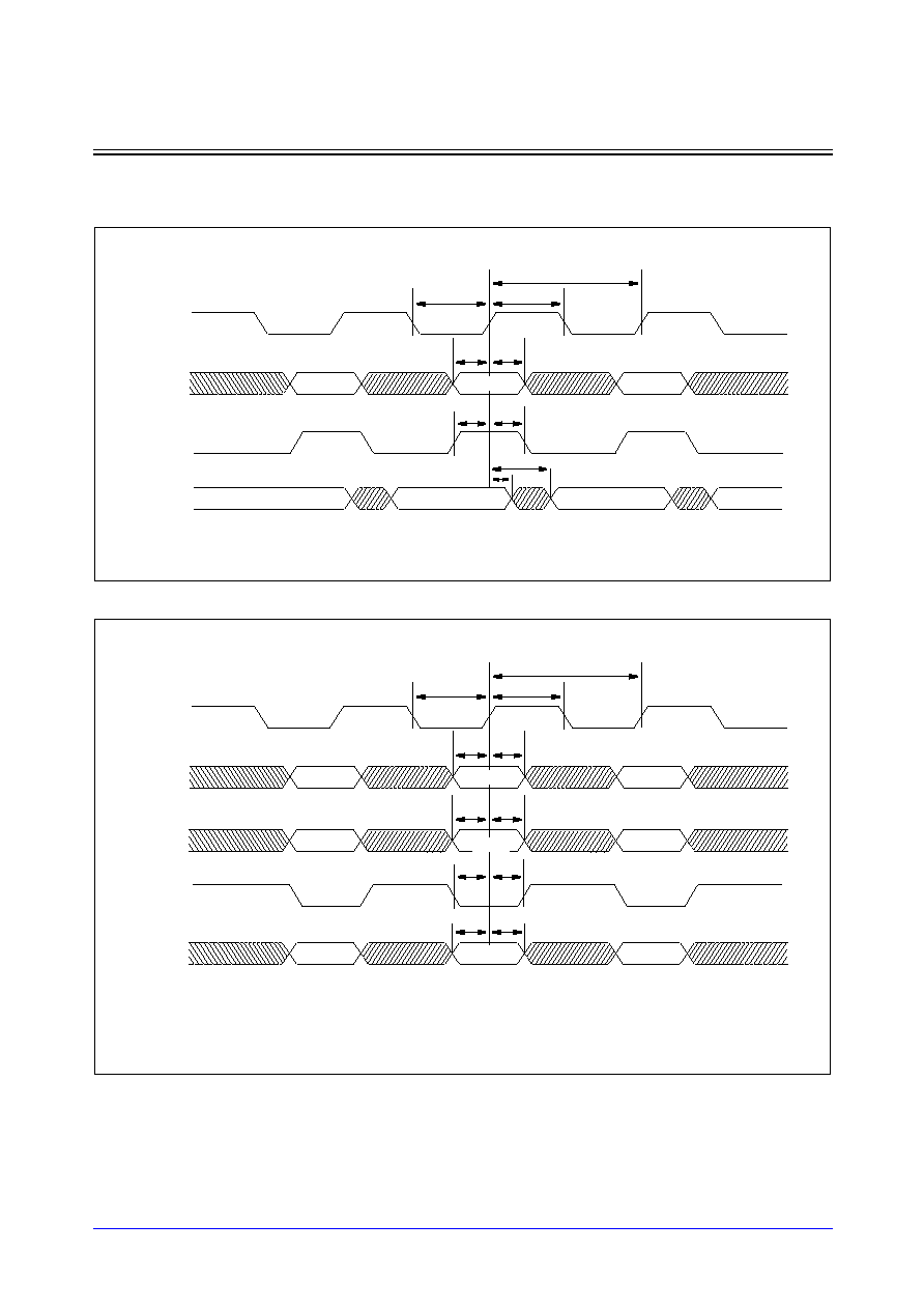
Samsung ASIC
5-69
STDL130
DPSRAMBW_HDL
High-Density Dual-Port Synchronous Static RAM with Bit-Write
Timing Diagrams
Read Cycle
Write Cycle
t
as
A[]
t
ah
(CSN = low, OEN = low, DI[], BWEN[]= don't care)
t
acc
WEN
t
ws
t
wh
t
da
DOUT[]
t
cyc
CK
t
ckl
t
ckh
A0
A2
Valid
M[A0]
M[A1]
M[A2]
A1
t
as
A[]
t
ah
(CSN= low, OEN = don't care)
WEN
t
ws
t
wh
DI[]
t
cyc
CK
t
ckl
t
ckh
A0
A2
A1
t
ds
t
dh
D0
D2
D1
t
bws
BWEN[]
t
bwh
BW0
BW2
BW1
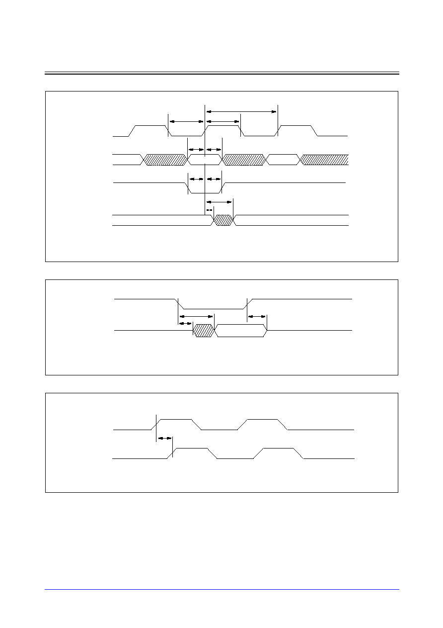
STDL130
5-70
Samsung ASIC
DPSRAMBW_HDL
High-Density Dual-Port Synchronous Static RAM with Bit-Write
Read Cycle with CSN-Controlled
OEN-Controlled Output Enable
Contention Mode
NOTE: "don't care" means the condition that these pins are in normal operation mode.
t
as
A[]
t
ah
(OEN = low, WEN = high, DI[], BWEN[] = don't care)
CSN
t
cs
t
ch
DOUT[]
t
cyc
CK
t
ckl
t
ckh
A0
A2
A1
t
da
t
acc
M[A1]
M[A0]
(CSN, CK, A[], WEN, DI[], BWEN[] = don't care)
t
od
t
dz
Hi-Z
VALID
OEN
DOUT[]
Hi-Z
t
zd
CK1
tcc
CK2
(A1[] = A2[])

Samsung ASIC
5-71
STDL130
DROM_HDL
High-Density Synchronous Diffusion Programmable ROM
Logic Symbol
Function Description
DROM_HDL is a synchronous diffusion programmable ROM which is provided as a compiler. DROM_HDL
is intended for use in high-density applications. The read cycle is initiated at the rising edge of CK. The data
at DOUT[] become valid after a delay. While in standby mode that CSN is high, DOUT[] remains stable.
When OEN is high, DOUT is placed in a high-impedance state.
DROM_HDL Function Table
CK
CSN
OEN
A
DOUT
Comment
X
X
H
X
Z
Unconditional tri-state output
X
H
L
X
DOUT(t-1)
De-selected (standby mode)
L
L
Valid
MEM(A)
Read cycle
Features
∑
Suitable for high-density applications
∑
Low-average power operation
∑
Diffusion-programmable code available
∑
Synchronous operation
∑
Duty-free clock cycle
∑
Asynchronous tri-state output
∑
Latched inputs and outputs
∑
Automatic power-down mode available
∑
Low noise output optimization
∑
Zero standby current
∑
Zero hold time
∑
Flexible aspect ratio
∑
Dual-bank scheme available
∑
Up to 512Kbits capacity
∑
Up to 16K number of words
∑
Up to 128 number of bits per word
CK
CSN
OEN
DOUT [b≠1:0]
drom_hdl_<w>x<b>m<y>b<ba>
A [m-1:0]
NOTES:
1. Words (w) is the number of words.
2. Bpw (b) is the number of bits per word.
3. Ymux (y) is one of the column mux types.
5. m =
log
2
w
4. Banks (ba) is the number of banks.
STDL130
5-72
Samsung ASIC
DROM_HDL
High-Density Synchronous Diffusion Programmable ROM
Parameter Description
DROM_HDL is the compiler that automatically generates symbol, netlist, timing model, power model and
layout according to the following parameters; Number of words(w), Number of bits per word(b) and Column
mux(y) and Number of banks(ba).
Pin Descriptions
Pin Capacitance
(Unit = SL)
NOTE: Each pin's capacitance is exactly same regardless of available mux types for same bank.
Parameters
Ymux(y) = 8
Ymux(y) = 16
Ymux(y) = 32
Words (w)
ba = 1
Min
64
128
256
Max
2048
4096
8192
Step
32
64
128
ba = 2
Min
128
256
512
Max
4096
8192
16384
Step
64
128
256
Bpw (b)
Min
2
2
2
Max
128
64
32
Step
1
1
1
Name
I/O
Description
CK
Clock
Clock input. CSN and A[] are latched into the ROM on the rising edge of CK. If CSN
is low on the rising edge of CK, the ROM is in read mode.
CSN
Chip
Enable
Chip enable input. The chip enable is active-low and is latched into the ROM on the
rising edge of CK. When CSN is low, the ROM is enabled for reading. When CSN is
high, the ROM goes to the standby mode and is disabled for reading. DOUT
remains previous data output.
OEN
Data
Output
Enable
Data output enable input. The data output enable is asynchronously operated
regardless of any inputs. When OEN is high, DOUT is disabled and goes to
high-impedance state.
A [ ]
Address
Address input bus. The address is latched into the ROM on the rising edge of CK.
DOUT [ ]
Data
Output
Data output bus. Data output is valid after the rising edge of CK while the ROM is in
read mode.
CK
CSN
OEN
A
DOUT
ba = 1
6.82
2.63
2.81
2.84
11.25
ba = 2
4.43
2.63
2.81
2.84
11.25
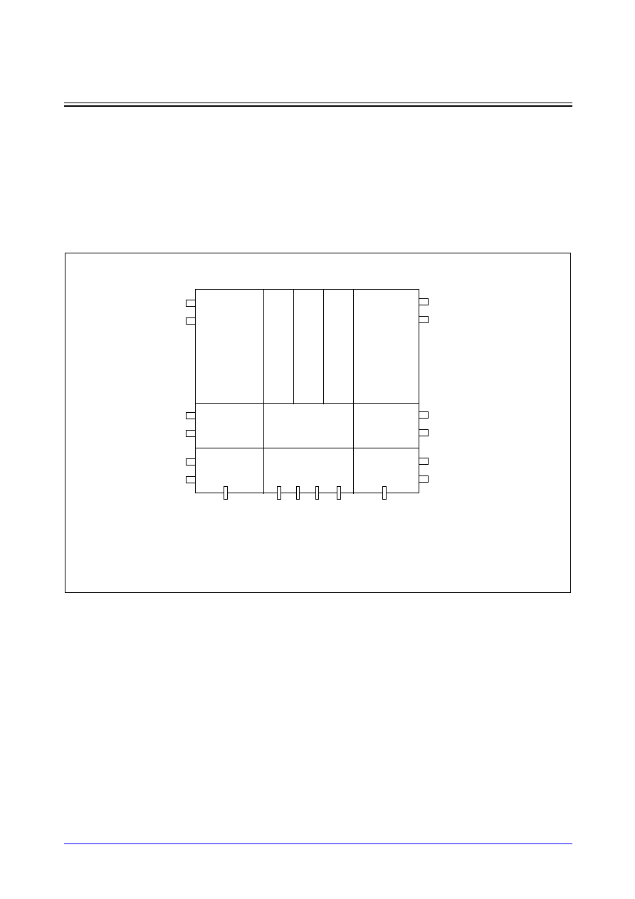
Samsung ASIC
5-73
STDL130
DROM_HDL
High-Density Synchronous Diffusion Programmable ROM
Block Diagrams
DROM_HDL has 2 different physical architectures due to the word depth. Optionally, one of these
architectures is generated from DROM_HDL compiler. In dual-bank, the bank selected by the address is
only activated while the other bank is in idle mode. In 1-bank architecture, the multi power ports are located
on the top edge, the middle edge and the bottom edge of both right- and left-sides of the memory. In 2-bank
architecture, the multi power ports are located on the top-edge, the middle-edge and the bottom-edge of
both right- and left-sides of the memory. All signal ports are only located on the bottom sides of the memory
regardless of architecture.
<1-bank architecture>
ROM Core
W
ord-line Decoder
X-Dec
W
ord-line Decoder
ROM Core
Y-Dec &
Sense Amp.
Control Block
Y-Dec &
Sense Amp.
Output Driver
Address &
Clock Buffers
Output Driver
VSS
VDD
VDD
VSS
VSS
VDD
VDD
VSS
CK
CSN
OEN
A[m-1:0]
DOUT[b-1:b/2]
DOUT[b/2-1:0]
VDD
VSS
VDD
VSS
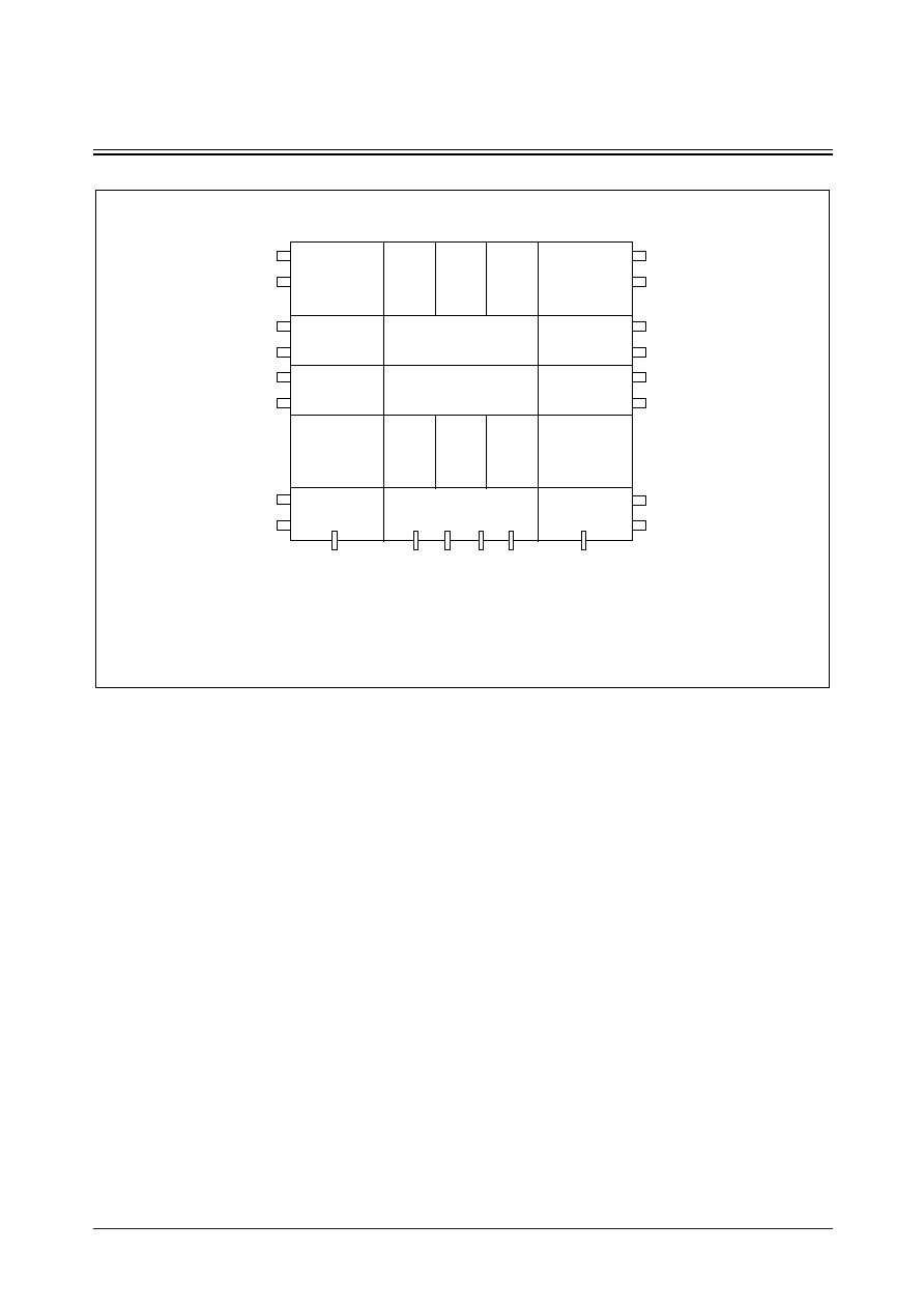
STDL130
5-74
Samsung ASIC
DROM_HDL
High-Density Synchronous Diffusion Programmable ROM
Application Notes
1.
Permitting over-the-cell routing
In chip-level layout, over-the-cell routing in DROM_HDL is permitted for only Metal-5 and Metal-6 layers.
2.
Incoming power bus should be adjusted to guarantee NOT more than 10% voltage drop at typical-case
current levels.
3.
Power stripe should be tapped from both sides of DROM_HDL.
4.
Power reduction during standby mode.
The standby power is measured on the condition that only CSN is in disable mode and other signals are
in operation mode except that OEN tied to low. If any of signals are activated while in standby mode, the
power will be consumed because the input switching activities are occurred by the signal transition.
Therefore, to reduce unnecessary power consumption, you should keep stable for all signals while in
standby mode.
<2-bank architecture >
ROM Core
W
ord-line
Decoder
X-Dec
W
ord-line
Decoder
ROM Core
Y-Dec &
Sense Amp.
Control Block
Y-Dec &
Sense Amp.
Y-Dec &
Sense Amp.
Control Block
Y-Dec &
Sense Amp.
ROM Core
W
ord-line
Decoder
X-Dec
W
ord-line
Decoder
ROM Core
Output Driver
Address &
Clock Buffers
Output Driver
VSS
VDD
VDD
VSS
VSS
VDD
VSS
VDD
VDD
VSS
VSS
VDD
CK
CSN
OEN
DOUT[b-1:b/2]
DOUT[b/2-1:0]
A[m-1:0]
VDD
VSS
VDD
VSS
Samsung ASIC
5-75
STDL130
DROM_HDL
High-Density Synchronous Diffusion Programmable ROM
Characteristics
Definition for AC Timing (ns)
Symbol
Description
Symbol
Description
t
cyc
Clock cycle time
t
ch
CSN hold time from CK rise
t
ckl
Clock pulse width low
t
acc
Data access time
t
ckh
Clock pulse width high
t
da
De-access time
t
as
Address setup time
t
dz
DOUT drive to high-Z time
t
ah
Address hold time
t
zd
DOUT high-Z to drive time
t
cs
CSN setup time
t
od
OEN to valid output
Definition for Power Consumption (
µ
W/MHz)
Power_read
The dynamic average power consumption while in a read cycle
Power_standby
The standby power consumption while CSN is high, OEN is low and other signals are in
normal operations
Definition for Area (
µ
m)
Width
The physical width in X-direction
Height
The physical height in Y-direction

STDL130
5-76
Samsung ASIC
DROM_HDL
High-Density Synchronous Diffusion Programmable ROM
Reference Table
* For Ymux=8
(Typical process, 1.8V, 25
∞
C, Output load=10SL, Input slope=0.2 ns, SA=0.5)
NOTE: Standby power is measured on the condition that other signals are in normal operation while CSN is in
disable mode and OEN is low.
Parameters
words
64
128
128
256
256
512
512
bpw
32
48
48
64
64
80
80
ba
1
1
2
1
2
1
2
Timing (ns)
t
cyc
3.21
3.28
3.51
3.35
3.58
3.44
3.67
t
ckl
0.81
0.81
0.91
0.81
0.92
0.81
0.94
t
ckh
1.20
1.20
1.35
1.20
1.36
1.20
1.37
t
as
0.35
0.34
0.91
0.34
0.92
0.33
0.94
t
ah
0.01
0.01
0.01
0.01
0.01
0.01
0.01
t
cs
0.81
0.81
0.91
0.81
0.92
0.81
0.94
t
ch
0.01
0.01
0.01
0.01
0.01
0.01
0.01
t
acc
2.32
2.40
2.60
2.49
2.69
2.60
2.81
t
da
1.95
2.04
2.19
2.13
2.28
2.27
2.42
t
dz
0.48
0.53
0.53
0.58
0.58
0.63
0.63
t
zd
0.63
0.67
0.67
0.71
0.71
0.75
0.75
t
od
0.71
0.75
0.75
0.79
0.79
0.83
0.83
Power (
µ
W/MHz)
Power_read
101.98
135.12
176.13
178.45
216.91
245.95
273.96
Power_standby
19.49
21.59
58.17
24.69
62.77
29.72
69.70
Area (
µ
m)
Width
426.10
581.87
579.88
739.63
735.65
901.36
893.41
Height
166.72
173.92
318.72
188.32
333.12
217.12
361.92

Samsung ASIC
5-77
STDL130
DROM_HDL
High-Density Synchronous Diffusion Programmable ROM
Reference Table
* For Ymux=8
(Typical process, 1.8V, 25
∞
C, Output load=10SL, Input slope=0.2 ns, SA=0.5)
NOTE: Standby power is measured on the condition that other signals are in normal operation while CSN is in
disable mode and OEN is low.
Parameters
words
1024
1024
1536
1536
2048
2048
4096
bpw
96
96
112
112
128
128
128
ba
1
2
1
2
1
2
2
Timing (ns)
t
cyc
3.59
3.79
3.76
3.93
3.93
4.07
4.39
t
ckl
0.81
0.97
0.81
1.00
0.81
1.03
1.16
t
ckh
1.20
1.41
1.20
1.44
1.20
1.47
1.60
t
as
0.31
0.97
0.30
1.00
0.28
1.03
1.16
t
ah
0.01
0.01
0.01
0.01
0.01
0.01
0.01
t
cs
0.81
0.97
0.81
1.00
0.81
1.03
1.16
t
ch
0.01
0.01
0.01
0.01
0.01
0.01
0.01
t
acc
2.76
2.96
2.97
3.14
3.19
3.32
3.69
t
da
2.45
2.60
2.64
2.77
2.84
2.95
3.26
t
dz
0.68
0.68
0.73
0.74
0.79
0.79
0.79
t
zd
0.79
0.79
0.83
0.83
0.87
0.88
0.87
t
od
0.87
0.87
0.91
0.91
0.95
0.95
0.95
Power (
µ
W/MHz)
Power_read
327.04
358.32
416.20
433.12
514.88
514.90
632.48
Power_standby
34.63
81.31
42.62
89.00
50.62
96.68
130.85
Area (
µ
m)
Width
1059.78
1055.14
1215.88
1211.24
1371.98
1367.34
1371.98
Height
274.72
419.52
332.32
477.12
389.92
534.72
765.12

STDL130
5-78
Samsung ASIC
DROM_HDL
High-Density Synchronous Diffusion Programmable ROM
Reference Table
* For Ymux=16
(Typical process, 1.8V, 25
∞
C, Output load=10SL, Input slope=0.2 ns, SA=0.5)
NOTE: Standby power is measured on the condition that other signals are in normal operation while CSN is in
disable mode and OEN is low.
Parameters
words
128
256
256
512
512
1024
1024
bpw
16
24
24
32
32
40
40
ba
1
1
2
1
2
1
2
Timing (ns)
t
cyc
3.21
3.28
3.51
3.35
3.58
3.45
3.67
t
ckl
0.80
0.81
0.91
0.81
0.92
0.81
0.94
t
ckh
1.20
1.20
1.35
1.20
1.36
1.20
1.37
t
as
0.35
0.34
0.91
0.34
0.92
0.33
0.94
t
ah
0.01
0.01
0.01
0.01
0.01
0.01
0.01
t
cs
0.80
0.81
0.91
0.82
0.92
0.81
0.94
t
ch
0.01
0.01
0.01
0.01
0.01
0.01
0.01
t
acc
2.36
2.44
2.66
2.52
2.75
2.63
2.88
t
da
1.95
2.04
2.20
2.14
2.30
2.28
2.43
t
dz
0.45
0.48
0.48
0.51
0.51
0.54
0.54
t
zd
0.60
0.63
0.63
0.65
0.65
0.68
0.68
t
od
0.68
0.71
0.71
0.73
0.73
0.76
0.76
Power (
µ
W/MHz)
Power_read
78.08
100.06
139.99
127.58
167.41
168.80
204.62
Power_standby
18.50
20.10
55.17
22.67
58.77
27.21
64.70
Area (
µ
m)
Width
426.10
581.87
579.88
739.63
735.65
901.36
893.41
Height
166.72
173.92
318.72
188.32
333.12
217.12
361.92

Samsung ASIC
5-79
STDL130
DROM_HDL
High-Density Synchronous Diffusion Programmable ROM
Reference Table
* For Ymux=16
(Typical process, 1.8V, 25
∞
C, Output load=10SL, Input slope=0.2 ns, SA=0.5)
NOTE: Standby power is measured on the condition that other signals are in normal operation while CSN is in
disable mode and OEN is low.
Parameters
words
2048
2048
3072
3072
4096
4096
8192
bpw
48
48
56
56
64
64
64
ba
1
2
1
2
1
2
2
Timing (ns)
t
cyc
3.59
3.79
3.76
3.93
3.93
4.07
4.39
t
ckl
0.81
0.97
0.81
1.00
0.81
1.03
1.16
t
ckh
1.20
1.41
1.20
1.44
1.20
1.47
1.60
t
as
0.31
0.97
0.30
1.00
0.28
1.03
1.16
t
ah
0.01
0.01
0.01
0.01
0.01
0.01
0.01
t
cs
0.81
0.97
0.81
1.00
0.81
1.03
1.16
t
ch
0.01
0.01
0.01
0.01
0.01
0.01
0.01
t
acc
2.80
3.03
3.01
3.21
3.23
3.39
3.76
t
da
2.46
2.61
2.65
2.78
2.85
2.97
3.27
t
dz
0.57
0.57
0.61
0.61
0.64
0.64
0.64
t
zd
0.71
0.71
0.73
0.74
0.76
0.76
0.76
t
od
0.79
0.79
0.82
0.82
0.84
0.84
0.84
Power (
µ
W/MHz)
Power_read
217.66
258.28
272.39
305.33
332.24
356.14
435.64
Power_standby
31.64
75.34
39.17
82.02
46.69
88.71
122.89
Area (
µ
m)
Width
1059.78
1055.14
1215.88
1211.24
1371.98
1367.34
1371.98
Height
274.72
419.52
332.32
477.12
389.92
534.72
765.12

STDL130
5-80
Samsung ASIC
DROM_HDL
High-Density Synchronous Diffusion Programmable ROM
Reference Table
* For Ymux=32
(Typical process, 1.8V, 25
∞
C, Output load=10SL, Input slope=0.2 ns, SA=0.5)
NOTE: Standby power is measured on the condition that other signals are in normal operation while CSN is in
disable mode and OEN is low.
Parameters
words
256
512
512
1024
1024
2048
2048
bpw
8
12
12
16
16
20
20
ba
1
1
2
1
2
1
2
Timing (ns)
t
cyc
3.21
3.28
3.52
3.35
3.58
3.44
3.67
t
ckl
0.81
0.81
0.91
0.81
0.92
0.81
0.94
t
ckh
1.20
1.20
1.35
1.20
1.36
1.20
1.37
t
as
0.34
0.34
0.91
0.34
0.92
0.33
0.94
t
ah
0.01
0.01
0.01
0.01
0.01
0.01
0.01
t
cs
0.81
0.81
0.91
0.81
0.92
0.81
0.94
t
ch
0.01
0.01
0.01
0.01
0.01
0.01
0.01
t
acc
2.42
2.51
2.79
2.59
2.88
2.70
3.00
t
da
1.97
2.06
2.22
2.15
2.32
2.29
2.45
t
dz
0.43
0.45
0.45
0.47
0.47
0.49
0.49
t
zd
0.59
0.60
0.60
0.62
0.62
0.64
0.64
t
od
0.67
0.69
0.69
0.70
0.70
0.72
0.72
Power (
µ
W/MHz)
Power_read
66.37
82.45
122.23
102.17
142.87
130.41
170.21
Power_standby
18.00
19.35
53.66
21.67
56.78
25.95
62.23
Area (
µ
m)
Width
426.10
581.87
579.88
739.63
735.65
901.36
893.41
Height
166.72
173.92
318.72
188.32
333.12
217.12
361.92

Samsung ASIC
5-81
STDL130
DROM_HDL
High-Density Synchronous Diffusion Programmable ROM
Reference Table
* For Ymux=32
(Typical process, 1.8V, 25
∞
C, Output load=10SL, Input slope=0.2 ns, SA=0.5)
NOTE: Standby power is measured on the condition that other signals are in normal operation while CSN is in
disable mode and OEN is low.
Parameters
words
4096
4096
6144
6144
8192
8192
16384
bpw
24
24
28
28
32
32
32
ba
1
2
1
2
1
2
2
Timing (ns)
t
cyc
3.59
3.79
3.76
3.93
3.93
4.07
4.39
t
ckl
0.81
0.97
0.81
1.00
0.81
1.03
1.16
t
ckh
1.20
1.41
1.20
1.44
1.20
1.47
1.60
t
as
0.31
0.97
0.30
1.00
0.28
1.03
1.16
t
ah
0.01
0.01
0.01
0.01
0.01
0.01
0.01
t
cs
0.81
0.97
0.81
1.00
0.81
1.03
1.16
t
ch
0.01
0.01
0.01
0.01
0.01
0.01
0.01
t
acc
2.87
3.16
3.09
3.34
3.31
3.53
3.90
t
da
2.47
2.63
2.67
2.80
2.87
2.99
3.29
t
dz
0.52
0.52
0.54
0.54
0.56
0.56
0.56
t
zd
0.66
0.66
0.68
0.68
0.70
0.71
0.70
t
od
0.74
0.74
0.76
0.76
0.78
0.78
0.78
Power (
µ
W/MHz)
Power_read
163.23
208.92
200.70
242.00
241.11
277.10
337.56
Power_standby
30.16
72.37
37.40
78.55
44.64
84.74
118.90
Area (
µ
m)
Width
1059.78
1055.14
1215.88
1211.24
1371.98
1367.34
1371.98
Height
274.72
419.52
332.32
477.12
389.92
534.72
765.12

STDL130
5-82
Samsung ASIC
DROM_HDL
High-Density Synchronous Diffusion Programmable ROM
Timing Diagrams
Read Cycle
Read Cycle with CSN Controlled
OEN-Controlled Output Enable
NOTE: "don't care" means the condition that these pins are in normal operation mode.
t
as
A[]
t
ah
(CSN, OEN = low)
t
acc
t
da
DOUT[]
t
cyc
CK
t
ckl
A0
A2
Valid
M[A0]
M[A1]
M[A2]
A1
t
ckh
(OEN = low)
t
ch
t
cs
CSN
DOUT[]
A1
A2
A0
A[]
t
as
t
ah
M[A1]
t
acc
t
da
CK
t
ckl
t
ckh
t
cyc
M[A0]
(CK, A, CSN = don't care)
t
od
t
dz
Hi-Z
VALID
OEN
DOUT
Hi-Z
t
zd
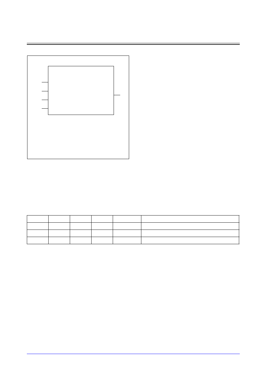
Samsung ASIC
5-83
STDL130
MROM_HDL
High-Density Synchronous Metal-2 Programmable ROM
Logic Symbol
Function Description
MROM_HDL is a synchronous metal-2 programmable ROM which is provided as a compiler. MROM_HDL is
intended for use in high-density applications. The read cycle is initiated at the rising edge of CK. The data at
DOUT[] become valid after a delay. While in standby mode that CSN is high, DOUT[] remains stable. When
OEN is high, DOUT is placed in a high-impedance state.
MROM_HDL Function Table
CK
CSN
OEN
A
DOUT
Comment
X
X
H
X
Z
Unconditional tri-state output
X
H
L
X
DOUT(t-1)
De-selected (standby mode)
L
L
Valid
MEM(A)
Read cycle
Features
∑
Suitable for high-density applications
∑
Low-average power operation
∑
Metal2-programmable code available
∑
Synchronous operation
∑
Duty-free clock cycle
∑
Asynchronous tri-state output
∑
Latched inputs and outputs
∑
Automatic power-down mode available
∑
Low noise output optimization
∑
Zero standby current
∑
Zero hold time
∑
Flexible aspect ratio
∑
Dual-bank scheme available
∑
Up to 512Kbits capacity
∑
Up to 16K number of words
∑
Up to 128 number of bits per word
CK
CSN
OEN
DOUT [b≠1:0]
mrom_hdl_<w>x<b>m<y>b<ba>
A [m-1:0]
NOTES:
1. Words (w) is the number of words.
2. Bpw (b) is the number of bits per word.
3. Ymux (y) is one of the column mux types.
5. m =
log
2
w
4. Banks (ba) is the number of banks.

STDL130
5-84
Samsung ASIC
MROM_HDL
High-Density Synchronous Metal-2 Programmable ROM
Parameter Description
MROM_HDL is the compiler that automatically generates symbol, netlist, timing model, power model and
layout according to the following parameters; Number of words(w), Number of bits per word(b), Column
mux(y) and Number of banks(ba).
Pin Descriptions
Pin Capacitance
(Unit = SL)
NOTE: Each pin's capacitance is exactly same regardless of available mux types for same bank.
Parameters
Ymux(y) = 8
Ymux(y) = 16
Ymux(y) = 32
Words (w)
ba = 1
Min
64
128
256
Max
2048
4096
8192
Step
32
64
128
ba = 2
Min
128
256
512
Max
4096
8192
16384
Step
64
128
256
Bpw (b)
Min
2
2
2
Max
128
64
32
Step
1
1
1
Name
I/O
Description
CK
Clock
Clock input. CSN and A[] are latched into the ROM on the rising edge of CK. If CSN
is low on the rising edge of CK, the ROM is in read mode.
CSN
Chip
Enable
Chip Enable input. The chip enable is active-low and is latched into the ROM on the
rising edge of CK. When CSN is low, the ROM is enabled for reading. When CSN is
high, the ROM goes to the standby mode and is disabled for reading. DOUT
remains previous data output.
OEN
Data
Output
Enable
Data output enable input. The data output enable is asynchronously operated
regardless of any inputs. When OEN is high, DOUT is disabled and goes to
high-impedance state.
A [ ]
Address
Address input bus. The address is latched into the ROM on the rising edge of CK.
DOUT [ ]
Data
Output
Data output bus. Data output is valid after the rising edge of CK while the ROM is in
read mode.
CK
CSN
OEN
A
DOUT
ba = 1
6.52
1.94
2.17
1.94
8.61
ba = 2
3.56
1.94
2.17
1.94
8.61
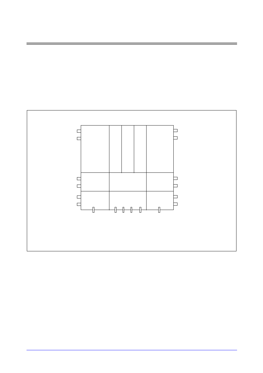
Samsung ASIC
5-85
STDL130
MROM_HDL
High-Density Synchronous Metal-2 Programmable ROM
Block Diagrams
MROM_HDL has 2 different physical architectures due to the word depth. Optionally, one of these
architectures is generated from MROM_HDL compiler. In dual-bank, the bank selected by the address is
only activated while the other bank is in idle mode. In 1-bank architecture, the multi power ports are located
on the top-edge, the middle edge and the bottom edge of both right- and left-sides of the memory. In 2-bank
architecture, the multi power ports are located on the top-edge, the middle-edge and the bottom-edge of
both right- and left-sides of the memory. All signal ports are only located on the bottom sides of the memory
regardless of architecture.
<1-bank architecture>
ROM Core
W
ord-line Decoder
X-Dec
W
ord-line Decoder
ROM Core
Y-Dec &
Sense Amp.
Control Block
Y-Dec &
Sense Amp.
Output Driver
Address &
Clock Buffers
Output Driver
VSS
VDD
VDD
VSS
VSS
VDD
VDD
VSS
CK
CSN
OEN
A[m-1:0]
DOUT[b/2:b-1]
DOUT[b/2-1:0]
VDD
VSS
VDD
VSS
STDL130
5-86
Samsung ASIC
MROM_HDL
High-Density Synchronous Metal-2 Programmable ROM
Application Notes
1.
Permitting over-the-cell routing. In chip-level layout, over-the-cell routing in MROM_HDL is permitted for
only Metal-5 and Metal-6 layers.
2.
Incoming power bus should be adjusted to guarantee NOT more than 10% voltage drop at typical-case
current levels.
3.
Power stripe should be tapped from both sides of MROM_HDL.
4.
Power reduction duting standby mode. The standby power is measured on the condition that only CSN
is in disable mode and other signals are in operation mode except that OEN is tied to low. If any of
signals are actived while in standby mode, the power will be consumed because the input switching
activities are occurred by the signal transition. Therefore, to reduce unnecessary power consumption,
you should keep stable for all signals while in standby mode.
<2-bank architecture >
ROM Core
W
ord-line
Decoder
X-Dec
W
ord-line
Decoder
ROM Core
Y-Dec &
Sense Amp.
Control Block
Y-Dec &
Sense Amp.
Y-Dec &
Sense Amp.
Control Block
Y-Dec &
Sense Amp.
ROM Core
W
ord-line
Decoder
X-Dec
W
ord-line
Decoder
ROM Core
Output Driver
Address &
Clock Buffers
Output Driver
VSS
VDD
VDD
VSS
VSS
VDD
VSS
VDD
VDD
VSS
VSS
VDD
CK
CSN
OEN
DOUT[b/2:b-1]
DOUT[b/2-1:0]
A[m-1:0]
VDD
VSS
VDD
VSS

Samsung ASIC
5-87
STDL130
MROM_HDL
High-Density Synchronous Metal-2 Programmable ROM
Characteristics
Definition for AC Timing (ns)
Symbol
Description
Symbol
Description
t
cyc
Clock cycle time
t
ch
CSN hold time from CK rise
t
ckl
Clock pulse width low
t
acc
Data access time
t
ckh
Clock pulse width high
t
da
De-access time
t
as
Address setup time
t
dz
DOUT drive to high-Z time
t
ah
Address hold time
t
zd
DOUT high-Z to drive time
t
cs
CSN setup time
t
od
OEN to valid data output
Definition for Power Consumption (
µ
W/MHz)
Power_read
The dynamic average power consumption while in a read cycle
Power_standby
The standby power consumption while CSN is high, OEN is low and other signals are in
normal operations
Definition for Area (
µ
m)
Width
The physical width in X-direction
Height
The physical height in Y-direction

STDL130
5-88
Samsung ASIC
MROM_HDL
High-Density Synchronous Metal-2 Programmable ROM
Reference Table
* For Ymux=8
(Typical process, 1.8V, 25
∞
C, Output load=10SL, Input slope=0.2 ns, SA=0.5)
NOTE: Standby power is measured on the condition that other signals are in normal operation while CSN is in
disable mode and OEN is low.
Parameters
words
64
128
128
256
256
512
512
bpw
32
48
48
64
64
80
80
ba
1
1
2
1
2
1
2
Timing (ns)
t
cyc
3.36
3.48
3.60
3.60
3.72
3.75
3.86
t
ckl
0.92
0.92
0.90
0.92
0.91
0.92
0.92
t
ckh
1.14
1.15
1.30
1.15
1.31
1.15
1.31
t
as
0.46
0.45
0.90
0.44
0.91
0.41
0.92
t
ah
0.01
0.01
0.01
0.01
0.01
0.01
0.01
t
cs
0.92
0.92
0.90
0.92
0.91
0.92
0.92
t
ch
0.01
0.01
0.01
0.01
0.01
0.01
0.01
t
acc
2.49
2.63
2.84
2.76
2.97
2.88
3.12
t
da
2.04
2.20
2.35
2.37
2.49
2.58
2.68
t
dz
0.50
0.57
0.56
0.62
0.62
0.68
0.68
t
zd
0.64
0.69
0.69
0.73
0.73
0.78
0.78
t
od
0.73
0.77
0.77
0.82
0.82
0.86
0.86
Power (
µ
W/MHz)
Power_read
106.08
148.89
189.67
206.78
240.68
297.72
310.48
Power_standby
22.14
24.48
63.95
27.64
68.94
32.48
75.89
Area (
µ
m)
Width
427.44
602.19
600.20
783.05
779.07
965.59
957.64
Height
166.70
179.98
320.12
206.54
346.68
259.66
399.80
Samsung ASIC
5-89
STDL130
MROM_HDL
High-Density Synchronous Metal-2 Programmable ROM
Reference Table
* For Ymux=8
(Typical process, 1.8V, 25
∞
C, Output load=10SL, Input slope=0.2 ns, SA=0.5)
NOTE: Standby power is measured on the condition that other signals are in normal operation while CSN is in
disable mode and OEN is low.
Parameters
words
1024
1024
1536
1536
2048
2048
4096
bpw
96
96
112
112
128
128
128
ba
1
2
1
2
1
2
2
Timing (ns)
t
cyc
3.95
4.05
4.19
4.23
4.42
4.42
4.69
t
ckl
0.92
0.93
0.92
0.95
0.92
0.97
1.04
t
ckh
1.15
1.33
1.15
1.35
1.15
1.36
1.43
t
as
0.36
0.93
0.35
0.95
0.34
0.97
1.04
t
ah
0.01
0.01
0.01
0.01
0.01
0.01
0.01
t
cs
0.92
0.93
0.92
0.95
0.92
0.97
1.04
t
ch
0.01
0.01
0.01
0.01
0.01
0.01
0.01
t
acc
3.15
3.30
3.44
3.54
3.72
3.76
4.11
t
da
2.83
2.94
3.12
3.16
3.40
3.40
3.70
t
dz
0.74
0.74
0.80
0.80
0.86
0.86
0.86
t
zd
0.83
0.83
0.87
0.87
0.92
0.92
0.92
t
od
0.91
0.91
0.96
0.96
1.01
1.01
1.01
Power (
µ
W/MHz)
Power_read
417.74
422.50
554.87
523.81
713.46
636.78
832.10
Power_standby
36.84
86.83
43.65
94.06
50.47
101.27
128.01
Area (
µ
m)
Width
1140.37
1135.73
1312.82
1308.18
1485.28
1480.64
1485.28
Height
365.90
506.04
472.14
612.28
578.38
718.52
1143.48
STDL130
5-90
Samsung ASIC
MROM_HDL
High-Density Synchronous Metal-2 Programmable ROM
Reference Table
* For Ymux=16
(Typical process, 1.8V, 25
∞
C, Output load=10SL, Input slope=0.2 ns, SA=0.5)
NOTE: Standby power is measured on the condition that other signals are in normal operation while CSN is in
disable mode and OEN is low.
Parameters
words
128
256
256
512
512
1024
1024
bpw
16
24
24
32
32
40
40
ba
1
1
2
1
2
1
2
Timing (ns)
t
cyc
3.36
3.48
3.60
3.60
3.72
3.75
3.86
t
ckl
0.92
0.92
0.90
0.93
0.91
0.93
0.92
t
ckh
1.14
1.15
1.30
1.15
1.31
1.15
1.31
t
as
0.46
0.45
0.90
0.44
0.91
0.41
0.92
t
ah
0.01
0.01
0.01
0.01
0.01
0.01
0.01
t
cs
0.92
0.92
0.90
0.93
0.91
0.93
0.92
t
ch
0.01
0.01
0.01
0.01
0.01
0.01
0.01
t
acc
2.52
2.67
2.89
2.79
3.03
2.91
3.18
t
da
2.05
2.21
2.36
2.38
2.51
2.59
2.70
t
dz
0.46
0.50
0.50
0.54
0.54
0.57
0.57
t
zd
0.61
0.64
0.64
0.67
0.67
0.70
0.70
t
od
0.69
0.72
0.72
0.75
0.75
0.78
0.78
Power (
µ
W/MHz)
Power_read
82.74
110.90
151.91
148.02
187.02
203.27
232.30
Power_standby
21.11
22.92
60.86
25.58
64.81
29.89
70.79
Area (
µ
m)
Width
427.44
602.55
600.56
783.05
779.07
965.34
957.39
Height
166.70
179.98
320.12
206.54
346.68
259.66
399.80

Samsung ASIC
5-91
STDL130
MROM_HDL
High-Density Synchronous Metal-2 Programmable ROM
Reference Table
* For Ymux=16
(Typical process, 1.8V, 25
∞
C, Output load=10SL, Input slope=0.2 ns, SA=0.5)
NOTE: Standby power is measured on the condition that other signals are in normal operation while CSN is in
disable mode and OEN is low.
Parameters
words
2048
2048
3072
3072
4096
4096
8192
bpw
48
48
56
56
64
64
64
ba
1
2
1
2
1
2
2
Timing (ns)
t
cyc
3.95
4.05
4.19
4.23
4.42
4.42
4.69
t
ckl
0.92
0.93
0.92
0.95
0.92
0.97
1.04
t
ckh
1.15
1.33
1.15
1.35
1.15
1.36
1.43
t
as
0.36
0.93
0.35
0.95
0.34
0.97
1.04
t
ah
0.01
0.01
0.01
0.01
0.01
0.01
0.01
t
cs
0.92
0.93
0.92
0.95
0.92
0.97
1.04
t
ch
0.01
0.01
0.01
0.01
0.01
0.01
0.01
t
acc
3.18
3.36
3.47
3.61
3.76
3.83
4.18
t
da
2.84
2.95
3.13
3.18
3.41
3.41
3.71
t
dz
0.61
0.61
0.65
0.65
0.69
0.69
0.69
t
zd
0.73
0.73
0.76
0.76
0.79
0.79
0.79
t
od
0.81
0.81
0.84
0.84
0.88
0.88
0.88
Power (
µ
W/MHz)
Power_read
274.20
300.98
351.83
362.76
438.43
430.58
540.03
Power_standby
33.76
80.76
40.07
86.91
46.38
93.06
119.79
Area (
µ
m)
Width
1140.37
1135.73
1312.82
1308.18
1485.28
1480.64
1485.28
Height
365.90
506.04
472.14
612.28
578.38
718.52
1143.48

STDL130
5-92
Samsung ASIC
MROM_HDL
High-Density Synchronous Metal-2 Programmable ROM
Reference Table
* For Ymux=32
(Typical process, 1.8V, 25
∞
C, Output load=10SL, Input slope=0.2 ns, SA=0.5)
NOTE: Standby power is measured on the condition that other signals are in normal operation while CSN is in
disable mode and OEN is low.
Parameters
words
256
512
512
1024
1024
2048
2048
bpw
8
12
12
16
16
20
20
ba
1
1
2
1
2
1
2
Timing (ns)
t
cyc
3.36
3.48
3.60
3.60
3.72
3.75
3.86
t
ckl
0.92
0.93
0.91
0.93
0.91
0.92
0.92
t
ckh
1.14
1.15
1.30
1.15
1.30
1.15
1.31
t
as
0.46
0.45
0.91
0.44
0.91
0.41
0.92
t
ah
0.01
0.01
0.01
0.01
0.01
0.01
0.01
t
cs
0.92
0.93
0.91
0.93
0.91
0.92
0.92
t
ch
0.01
0.01
0.01
0.01
0.01
0.01
0.01
t
acc
2.58
2.73
3.01
2.85
3.15
2.97
3.30
t
da
2.06
2.22
2.37
2.39
2.53
2.60
2.71
t
dz
0.44
0.46
0.46
0.49
0.49
0.52
0.52
t
zd
0.59
0.61
0.61
0.63
0.63
0.66
0.66
t
od
0.67
0.69
0.69
0.72
0.72
0.74
0.74
Power (
µ
W/MHz)
Power_read
71.12
92.24
133.37
118.76
159.84
156.07
192.78
Power_standby
20.59
22.15
59.30
24.55
62.75
28.61
68.21
Area (
µ
m)
Width
427.44
603.46
601.47
783.05
779.07
964.80
956.85
Height
166.70
179.98
320.12
206.54
346.68
259.66
399.80
Samsung ASIC
5-93
STDL130
MROM_HDL
High-Density Synchronous Metal-2 Programmable ROM
Reference Table
* For Ymux=32
(Typical process, 1.8V, 25
∞
C, Output load=10SL, Input slope=0.2 ns, SA=0.5)
NOTE: Standby power is measured on the condition that other signals are in normal operation while CSN is in
disable mode and OEN is low.
Parameters
words
4096
4096
6144
6144
8192
8192
16384
bpw
24
24
28
28
32
32
32
ba
1
2
1
2
1
2
2
Timing (ns)
t
cyc
3.95
4.05
4.18
4.23
4.42
4.42
4.69
t
ckl
0.92
0.93
0.92
0.95
0.92
0.97
1.04
t
ckh
1.15
1.33
1.15
1.35
1.15
1.36
1.43
t
as
0.37
0.93
0.35
0.95
0.34
0.97
1.04
t
ah
0.01
0.01
0.01
0.01
0.01
0.01
0.01
t
cs
0.92
0.93
0.92
0.95
0.92
0.97
1.04
t
ch
0.01
0.01
0.01
0.01
0.01
0.01
0.01
t
acc
3.25
3.48
3.54
3.73
3.83
3.95
4.31
t
da
2.85
2.96
3.14
3.19
3.42
3.43
3.73
t
dz
0.54
0.54
0.57
0.57
0.60
0.60
0.60
t
zd
0.68
0.68
0.70
0.70
0.72
0.72
0.72
t
od
0.76
0.76
0.78
0.78
0.81
0.81
0.81
Power (
µ
W/MHz)
Power_read
202.26
240.42
253.23
282.41
309.17
327.62
402.51
Power_standby
32.22
77.66
38.26
83.30
44.32
88.95
115.65
Area (
µ
m)
Width
1139.84
1135.20
1312.56
1307.92
1485.28
1480.64
1485.28
Height
365.90
506.04
472.14
612.28
578.38
718.52
1143.48
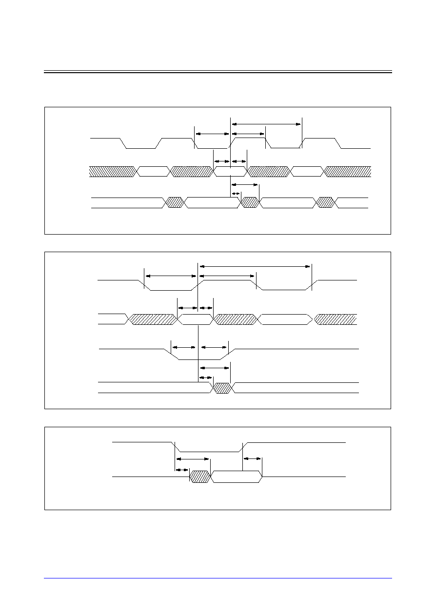
STDL130
5-94
Samsung ASIC
MROM_HDL
High-Density Synchronous Metal-2 Programmable ROM
Timing Diagrams
Read Cycle
Read Cycle with CSN Controlled
OEN-Controlled Output Enable
NOTE: "don't care" means the condition that these pins are in normal operation mode.
t
as
A[]
t
ah
(CSN, OEN = low)
t
acc
t
da
DOUT[]
t
cyc
CK
t
ckl
A0
A2
Valid
M[A0]
M[A1]
M[A2]
A1
t
ckh
(OEN = low)
t
ch
t
cs
CSN
DOUT[]
A1
A2
A0
A[]
t
as
t
ah
M[A1]
t
acc
t
da
CK
t
ckl
t
ckh
t
cyc
M[A0]
(CK, A, CSN = don't care)
t
od
t
dz
Hi-Z
Valid
OEN
DOUT
Hi-Z
t
zd
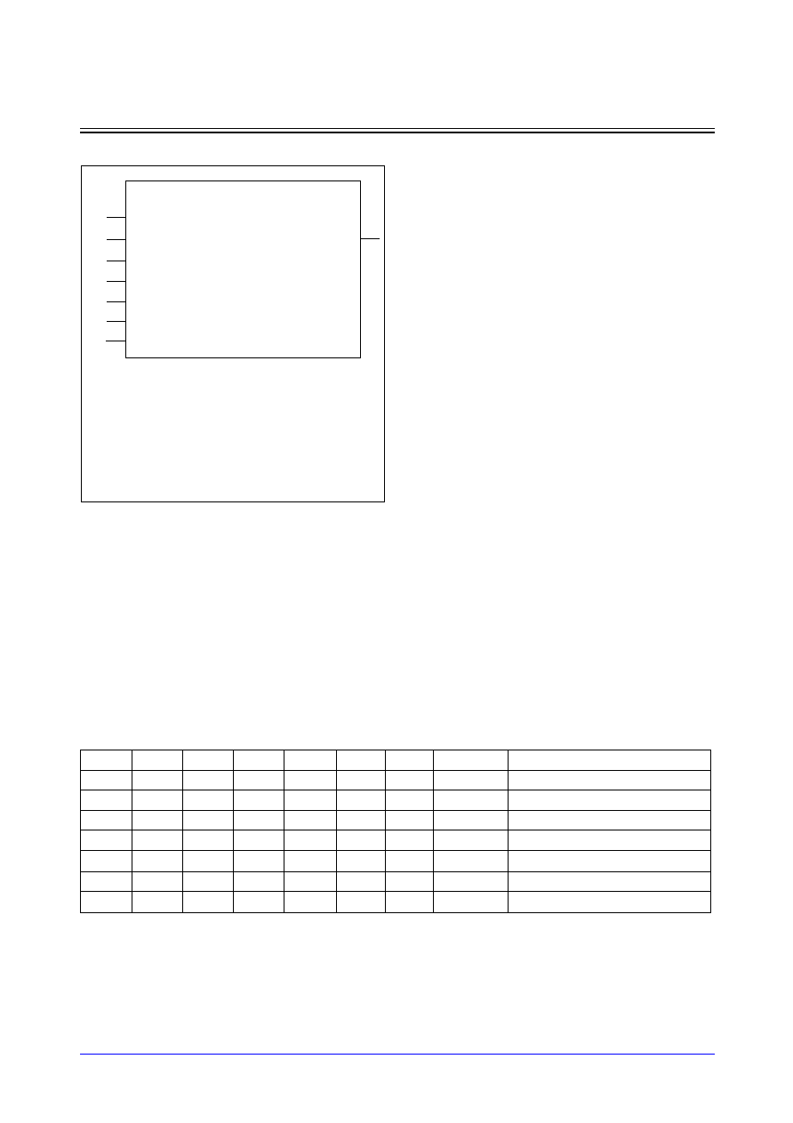
Samsung ASIC
5-95
STDL130
ARFRAM_HDL
High-Density Multi-Port Asynchronous Register File
Logic Symbol
Function Description
ARFRAM_HDL is a multi-port asynchronous register file which is provided as a compiler. ARFRAM_HDL is
intended for use in high-density applications. It allows maximum 4 ports with configurable 1-to-2 read ports
and 1-to-2 write ports. All read and write ports are fully independent. On the rising edge of CK, the write
cycle is initiated when WEN is low. While CK is high, the data at DI[] is written into the memory location
specified on WA[]. At the falling edge of CK, the write cycle is terminated. If WEN is high, WA[] and DI[] are
disabled . It is called "write standby mode". When REN and OEN are low, the data stored in the memory
location specified on RA[] becomes valid through DOUT[] after a delay. If REN is high, RA[] is disabled and
DOUT[] remains in the previous data output. It is called "read standby mode". When OEN is high, DOUT[] is
placed in a high-impedance state regardless of REN.
ARFRAM_HDL Function Table
CK
WEN
WA
DI
RA
REN
OEN
DOUT
Comment
X
H
X
X
X
X
X
X
Write standby mode
L
Valid
Valid
X
X
X
X
Write cycle starts
L
X
X
X
X
X
X
Write cycle ends
X
X
X
X
X
X
H
Z
Unconditional tri-state output
X
X
X
X
X
H
L
DOUT(t-1)
Read standby mode
X
X
X
X
Toggle
L
L
MEM(RA)
Read cycle
X
X
X
X
Valid
L
MEM(RA)
Read cycle with REN-controlled
Features
∑
High-density application
∑
Suitable for high-speed application
∑
Synchronous write operation
∑
Asynchronous read operation
∑
Fully independent port
∑
Latched input and output
∑
Separated data I/O
∑
Flexible aspect ratio
∑
Asynchronous tristate output
∑
Zero standby current
∑
Configurable 1-to-2 read ports
∑
Configurable 1-to-2 write ports
∑
Up to 16Kbits capacity
∑
Up to 1024K number of words
∑
Up to 64 number of bits per word
CK<nw-1>
WA<nw-1>[m-1:0]
REN<nr-1>
DOUT<nr-1>[b≠1:0]
arfram_hdl_<nr>r<nw>w_<w>x<b>m<y>
RA<nr-1>[m-1:0]
NOTES:
1. Words(w) is the number of words.
2. Bpw(b) is the number of bits per word.
3. Ymux(y) is one of the column mux types.
6. m =
log
2
w
5. Reads(nr) is the number of read ports(1-to-2).
4. Writes(nw) is the number of write ports(1-to-2).
WEN<nw-1>
DI<nw-1>[b-1:0]
OEN<nr-1>
STDL130
5-96
Samsung ASIC
ARFRAM_HDL
High-Density Multi-Port Asynchronous Register File
Parameter Description
ARFRAM_HDL is the compiler that automatically generates symbol, netlist, timing model, power model and
layout according to the following parameters; Number of words(w), Number of bit per word(b), Column
mux(y), Number of read ports(nr) and Number of write ports(nw).
Pin Descriptions
Parameters
Ymux(y) = 2
Ymux(y) = 4
Ymux(y) = 8
Words (w)
Min
4
8
16
Max
256
512
1024
Step
2
4
8
Bpw (b)
Min
1
1
1
Max
64
32
16
Step
1
1
1
Write ports(nw)
1, 2
Read ports(nr)
1, 2
Name
I/O
Description
CK<nw-1>
Write Clock
Write clock input on each write port. WEN, WA[] and DI[] are latched into the
RAM on the rising edge of CK. If WEN is low on the rising edge of CK, the RAM
is in write mode. If WEN is high on the rising edge of CK, the RAM is in write
standby mode. At the falling edge of CK, the write-operation completes and the
RAM is in a precharge state.
WEN<nw-1>
Write Enable
Write enable input on each write port. WEN is latched into the RAM on the rising
edge of CK. When WEN is low, the write mode is enabled. When WEN is high, it
prevents the write-operation. It is called "write standby mode".
WA<nw-1> [ ]
Write Address
Write address bus on each write port. It specifies the location in which the data
will be written in the write-operation. WA[] is latched at the rising edge of CK.
DI<nw-1> [ ]
Data Input
Data input bus on each write port. It contains data values to be written into the
memory during the write-cycle. DI[] is latched at the rising edge of CK.
REN<nr-1>
Read Enable
Read enable input on each read port. When REN is low, read is enabled. When
REN is high, read is disabled and DOUT[] remains in the previous state. It is
called "read standby mode"
OEN<nr-1>
Data Output
Enable
Output enable input on each read port. The low state enables output drivers and
the high state disables output to go to the Hi-Z state.
RA<nr-1> [ ]
Read Address
Read address bus on each read port. It specifies the location to be read in the
read-operation.
DOUT<nr-1> [ ]
Data Output
Data output bus on each read port. When REN and OEN are low, it presents the
data word stored in the location specified by RA[]. When REN is high and OEN
is low, DOUT[] remains in the previous state. When OEN is high, DOUT[] is in
the high-impedance state regardless of REN.
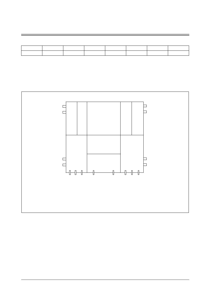
Samsung ASIC
5-97
STDL130
ARFRAM_HDL
High-Density Multi-Port Asynchronous Register File
Pin Capacitance
(Unit = SL)
Block Diagrams
ARFRAM_HDL supports only 1-bank architecture. The power ports are located on the top-edge and the
bottom edge of both right- and left-sides of the memory. All signal ports are only located on the bottom sides
of the memory.
CK
WEN
DI
REN
OEN
WA
RA
DOUT
3.29
11.44
5.55
9.28
3.95
3.29
5.74
32.30
Wr
ite Decoder
Wr
ite Buff
er
RAM Core
Read Buff
er
Read Decoder
Write
Control Block
Column Mux
Read
Control Block
I/O Driver
VSS
VDD
VDD
VSS
VSS
VDD
VDD
VSS
DOUT<nr-1>[b-1:0]
DI<nw-1>[b-1:0]
OEN<nr-1>
WEN<nw-1>
RA<nr-1>[m-1:0]
REN<nr-1>
CK<nw-1>
W
A<nw-1>[m-1:0]

STDL130
5-98
Samsung ASIC
ARFRAM_HDL
High-Density Multi-Port Asynchronous Register File
Application Notes
1.
Permitting over-the-cell routing.
In ARFRAM_HDL, the over-the-cell routing is permitted for Metal-4 or upper layers. Namely, while doing
layout on the chip-level, any signals to be routed can be crossed over the area of register file generated
by ARFRAM_HDL compiler.
2.
Incoming power bus should be adjusted to guarantee NOT more than 10% voltage drop at typical-case
current levels.
3.
Power stripe should be tapped from both sides of ARFRAM_HDL.
4.
Contention mode under same addresses(RA[]=WA[] or WA0[] = WA1[]).
In ARFRAM_HDL, simultaneous operations by both ports on the same address(RA[]=WA[] or WA0[] =
WA1[]) such as read/write,write/read, write/write operation, cause a contention problem. Simultaneous
operations are defined as the state in which both ports are enabled and both address buses are equal.
ARFRAM_HDL has no scheme preventing the contention mode. Due to the simultaneous operations,
silicon will behave unpredictably. A write operation cannot completes and data appearing at outputs may
not be valid.
Please refer to the timing diagrams if you want to avoid the contention mode between both ports.
5.
Keeping the stable address cycle time in read mode.
In ARFRAM_HDL, rather than the write operation which is synchronously performed by CK signal, the
read operation is asynchronously performed whenever the address transition occures. So, in read
mode if the another transition on the address occures after first transition within access time, read
operation cannot completes. At that time, while in the read operation, the data stored in the memory
may be corrupted due to the short transition. To prevent such fail, the stable read address cycle time
(trcyc) is required. The essential requirement to recognize valid read address transition is that at least
minimum address period should be equal or greater than tacc (access time).
6.
Power reduction during standby mode.
ARFRAM_HDL provides two types of standby modes ≠ the write standby mode and the read standby
mode. While in the write standby mode, WA[] and DI[] except CK are blocked even though the
transitions of those signals occure. While in the read standby mode, RA[] is blocked even though its
transition occures. So, you can reduce the power consumption in ARFRAM_HDL by properly using two
standby modes in your design.

Samsung ASIC
5-99
STDL130
ARFRAM_HDL
High-Density Multi-Port Asynchronous Register File
Characteristics
Definition for AC Timing (ns)
Symbol
Description
t
wcyc
Miminum write clock cycle time for write cycle
t
ckl
Mimimum CK pulse width low to guarantee write cycle
t
ckh
Mimimum CK pulse width high to guarantee write cycle
t
was
Write Address Setup time from WA[] to CK rise
t
wah
Write Address Hold time from CK rise to WA[]
t
ws
WEN Setup time from WEN fall to CK rise
t
wh
WEN Hold time from CK rise to WEN rise
t
ds
Data-in Setup time from DI[] to CK rise
t
dh
Data-in Hold time from CK rise to DI[]
t
wwc
Write-Write contention time from one CK to the other CK
t
wda
De-access time from CK rise to DOUT
t
wacc
Data Access time from CK fall
t
rcyc
Miminum RA[] Cycle time for read cycle
t
acc
Data ACCess time for read cycle
t
ras
Read Address Setup time from RA[] to REN rise
t
rah
Read Address Hold time from REN rise to RA[]
t
da
De-Access time
from RA to DOUT
t
zd
DOUT high-Z to Drive time
t
dz
DOUT Drive to high-Z time
t
od
OEN to valid output time
Definition for Power Consumption (
µ
W/MHz)
Power_read
The dynamic average power consumption while in a read cycle
Power_write
The dynamic average power consumption while in a write cycle
Power_w_standby
The write standby power consumption while WEN is high and other signals are in
normal operations.
Power_r_standby
The read standby power consumption while REN is high, OEN is low and other sig-
nals are in normal operations.
Definition for Area (
µ
m)
Width
The physical width in X-direction
Height
The physical height in Y-direction
STDL130
5-100
Samsung ASIC
ARFRAM_HDL
High-Density Multi-Port Asynchronous Register File
Reference Table
* For Ymux=2(nr=1, nw=1)
(Typical process, 1.8V, 25
∞
C, Output load=10SL, Input slope=0.2 ns, SA=0.5)
NOTE: SL is a standard load and SA is an input switching activity ratio during a clock.
Parameters
words
32
64
128
256
bpw
8
16
32
64
Timing (ns)
t
wcyc
1.39
1.53
1.81
2.54
t
ckl
1.08
1.06
1.03
1.08
t
ckh
0.26
0.29
0.38
0.69
t
was
0.75
0.72
0.65
0.62
t
wah
0.01
0.01
0.01
0.01
t
ws
0.15
1.13
1.10
1.15
t
wh
0.42
0.42
0.41
0.41
t
ds
0.84
0.80
0.73
0.71
t
dh
0.01
0.01
0.01
0.01
t
wda
1.94
2.19
2.38
2.71
t
wacc
1.99
2.22
2.38
2.84
t
rcyc
2.19
2.43
2.65
3.39
t
acc
2.19
2.43
2.65
3.39
t
ras
0.44
0.44
0.44
0.43
t
rah
0.14
0.15
0.16
0.18
t
da
0.93
0.99
1.11
1.31
t
zd
0.32
0.34
0.37
0.41
t
dz
0.28
0.30
0.35
0.39
t
od
0.62
0.65
0.71
0.84
Power (
µ
W/MHz)
Power_read
13.12
26.28
72.25
156.47
Power_write
22.32
43.46
93.98
262.00
Power_w_standby
1.51
2.25
3.70
6.51
Power_r_standby
0.10
0.12
0.25
0.36
Area (
µ
m)
Width
174.54
256.82
408.58
708.18
Height
216.88
297.20
472.80
824.00
Samsung ASIC
5-101
STDL130
ARFRAM_HDL
High-Density Multi-Port Asynchronous Register File
Reference Table
* For Ymux=4(nr=1, nw=1)
(Typical process, 1.8V, 25
∞
C, Output load=10SL, Input slope=0.2 ns, SA=0.5)
NOTE: SL is a standard load and SA is an input switching activity ratio during a clock.
Parameters
words
64
128
256
512
bpw
4
8
16
32
Timing (ns)
t
wcyc
1.40
1.53
1.79
2.46
t
ckl
1.09
1.08
1.06
1.06
t
ckh
0.26
0.28
0.38
0.67
t
was
0.77
0.74
0.70
0.64
t
wah
0.01
0.01
0.01
0.01
t
ws
1.16
1.15
1.12
1.12
t
wh
0.42
0.42
0.41
0.41
t
ds
0.85
0.82
0.78
0.72
t
dh
0.01
0.01
0.01
0.01
t
wda
1.96
2.21
2.40
2.72
t
wacc
2.02
2.24
2.40
2.86
t
rcyc
2.20
2.44
2.66
3.41
t
acc
2.20
2.44
2.66
3.41
t
ras
0.44
0.44
0.44
0.43
t
rah
0.14
0.15
0.16
0.17
t
da
0.93
0.97
1.06
1.22
t
zd
0.31
0.33
0.36
0.38
t
dz
0.27
0.29
0.32
0.36
t
od
0.61
0.63
0.67
0.76
Power (
µ
W/MHz)
Power_read
11.53
22.69
63.29
139.75
Power_write
23.13
42.45
89.56
235.72
Power_w_standby
1.92
2.33
3.07
4.52
Power_r_standby
0.10
0.13
0.25
0.36
Area (
µ
m)
Width
174.54
256.82
408.58
708.18
Height
216.88
297.20
472.80
824.00

STDL130
5-102
Samsung ASIC
ARFRAM_HDL
High-Density Multi-Port Asynchronous Register File
Reference Table
* For Ymux=8(nr=1, nw=1)
(Typical process, 1.8V, 25
∞
C, Output load=10SL, Input slope=0.2 ns, SA=0.5)
NOTE: SL is a standard load and SA is an input switching activity ratio during a clock.
Parameters
words
128
256
512
1024
bpw
2
4
8
16
Timing (ns)
t
wcyc
1.44
1.55
1.80
2.43
t
ckl
1.10
1.09
1.08
1.07
t
ckh
0.27
0.27
0.36
0.64
t
was
0.78
0.76
0.73
0.68
t
wah
0.01
0.01
0.01
0.01
t
ws
1.16
1.15
1.14
1.14
t
wh
0.42
0.42
0.43
0.41
t
ds
0.86
0.84
0.81
0.76
t
dh
0.01
0.01
0.01
0.01
t
wda
2.01
2.26
2.44
2.77
t
wacc
2.06
2.28
2.44
2.90
t
rcyc
2.23
2.47
2.69
3.45
t
acc
2.23
2.47
2.69
3.45
t
ras
0.44
0.44
0.44
0.43
t
rah
0.14
0.15
0.16
0.17
t
da
0.94
0.98
1.06
1.19
t
zd
0.30
0.32
0.33
0.38
t
dz
0.27
0.28
0.31
0.34
t
od
0.60
0.62
0.65
0.73
Power (
µ
W/MHz)
Power_read
10.93
20.97
59.50
130.82
Power_write
24.73
42.90
87.22
221.55
Power_w_standby
2.49
2.74
3.14
3.94
Power_r_standby
0.11
0.13
0.24
0.35
Area (
µ
m)
Width
174.54
256.82
408.58
708.18
Height
216.88
297.20
472.80
824.00

Samsung ASIC
5-103
STDL130
ARFRAM_HDL
High-Density Multi-Port Asynchronous Register File
Reference Table
* For Ymux=2(nr=1, nw=2)
(Typical process, 1.8V, 25
∞
C, Output load=10SL, Input slope=0.2 ns, SA=0.5)
NOTE: SL is a standard load and SA is an input switching activity ratio during a clock.
Parameters
words
32
64
128
256
bpw
8
16
32
64
Timing (ns)
t
wcyc
1.51
1.73
2.16
3.36
t
ckl
0.61
0.60
0.63
1.30
t
ckh
0.26
0.30
0.46
0.95
t
was
0.92
0.88
0.81
0.77
t
wah
0.01
0.01
0.01
0.01
t
ws
1.35
1.33
1.30
1.36
t
wh
0.27
0.27
0.27
0.27
t
ds
1.01
0.97
0.90
0.86
t
dh
0.01
0.01
0.01
0.01
t
wwc
0.26
0.30
0.46
0.95
t
wda
2.08
2.44
2.66
3.00
t
wacc
2.01
2.29
2.55
3.13
t
rcyc
2.19
2.43
2.65
3.39
t
acc
2.19
2.43
2.65
3.39
t
ras
0.44
0.44
0.44
0.43
t
rah
0.14
0.15
0.16
0.18
t
da
0.93
0.99
1.11
1.31
t
zd
0.32
0.34
0.37
0.41
t
dz
0.28
0.30
0.35
0.39
t
od
0.62
0.65
0.71
0.84
Power (
µ
W/MHz)
Power_read
13.12
26.28
72.25
156.47
Power_write
22.61
47.55
108.79
327.22
Power_w_standby
1.23
2.01
3.57
6.91
Power_r_standby
0.10
0.12
0.25
0.36
Area (
µ
m)
Width
261.44
392.38
627.22
1088.62
Height
208.86
291.74
469.42
824.78
STDL130
5-104
Samsung ASIC
ARFRAM_HDL
High-Density Multi-Port Asynchronous Register File
Reference Table
* For Ymux=4(nr=1, nw=2)
(Typical process, 1.8V, 25
∞
C, Output load=10SL, Input slope=0.2 ns, SA=0.5)
NOTE: SL is a standard load and SA is an input switching activity ratio during a clock.
Parameters
words
64
128
256
512
bpw
4
8
16
32
Timing (ns)
t
wcyc
1.53
1.74
2.17
3.36
t
ckl
0.62
0.61
0.63
1.30
t
ckh
0.26
0.30
0.46
0.95
t
was
0.94
0.91
0.87
0.79
t
wah
0.01
0.01
0.01
0.01
t
ws
1.36
1.35
1.33
1.34
t
wh
0.27
0.27
0.27
0.27
t
ds
1.03
0.27
0.96
0.88
t
dh
0.01
0.01
0.01
0.01
t
wwc
0.26
0.30
0.46
0.95
t
wda
2.14
2.51
2.73
3.08
t
wacc
2.07
2.35
2.61
3.19
t
rcyc
2.20
2.44
2.66
3.41
t
acc
2.20
2.44
2.66
3.41
t
ras
0.44
0.44
0.44
0.43
t
rah
0.14
0.15
0.16
0.17
t
da
0.93
0.97
1.06
1.22
t
zd
0.31
0.33
0.36
0.38
t
dz
0.27
0.29
0.32
0.36
t
od
0.61
0.63
0.67
0.82
Power (
µ
W/MHz)
Power_read
11.53
22.69
63.29
139.75
Power_write
23.68
47.39
105.72
326.95
Power_w_standby
1.31
1.80
2.67
4.63
Power_r_standby
0.10
0.13
0.25
0.36
Area (
µ
m)
Width
261.44
392.38
627.22
1088.62
Height
208.86
291.74
469.42
824.78

Samsung ASIC
5-105
STDL130
ARFRAM_HDL
High-Density Multi-Port Asynchronous Register File
Reference Table
* For Ymux=8(nr=1, nw=2)
(Typical process, 1.8V, 25
∞
C, Output load=10SL, Input slope=0.2 ns, SA=0.5)
NOTE: SL is a standard load and SA is an input switching activity ratio during a clock.
Parameters
words
128
256
512
1024
bpw
2
4
8
16
Timing (ns)
t
wcyc
1.58
1.75
2.18
3.37
t
ckl
0.63
0.63
0.63
1.30
t
ckh
0.30
0.30
0.44
0.93
t
was
0.95
0.93
0.89
0.84
t
wah
0.01
0.01
0.01
0.01
t
ws
1.36
1.36
1.34
1.34
t
wh
0.27
0.27
0.27
0.27
t
ds
1.04
1.02
0.98
0.93
t
dh
0.01
0.01
0.01
0.01
t
wwc
0.30
0.30
0.44
0.93
t
wda
2.26
2.64
2.88
3.23
t
wacc
2.19
2.48
2.73
3.32
t
rcyc
2.23
2.47
2.69
3.45
t
acc
2.23
2.47
2.69
3.45
t
ras
0.44
0.44
0.44
0.43
t
rah
0.14
0.15
0.16
0.17
t
da
0.94
0.98
1.06
1.19
t
zd
0.30
0.32
0.33
0.38
t
dz
0.27
0.28
0.31
0.34
t
od
0.60
0.62
0.65
0.73
Power (
µ
W/MHz)
Power_read
10.93
20.97
59.50
130.82
Power_write
25.29
46.33
105.59
323.34
Power_w_standby
1.64
1.80
2.40
3.51
Power_r_standby
0.11
0.13
0.24
0.35
Area (
µ
m)
Width
261.44
392.38
627.22
1088.62
Height
208.86
291.74
469.42
824.78
STDL130
5-106
Samsung ASIC
ARFRAM_HDL
High-Density Multi-Port Asynchronous Register File
Reference Table
* For Ymux=2(nr=2, nw=1)
(Typical process, 1.8V, 25
∞
C, Output load=10SL, Input slope=0.2 ns, SA=0.5)
NOTE: SL is a standard load and SA is an input switching activity ratio during a clock.
Parameters
words
32
64
128
256
bpw
8
16
32
64
Timing (ns)
t
wcyc
1.39
1.53
1.81
2.54
t
ckl
1.08
1.06
1.03
1.08
t
ckh
0.26
0.29
0.38
0.69
t
was
0.75
0.72
0.65
0.62
t
wah
0.01
0.01
0.01
0.01
t
ws
1.15
1.13
1.10
1.15
t
wh
0.42
0.42
0.41
0.41
t
ds
0.84
0.80
0.73
0.71
t
dh
0.01
0.01
0.01
0.01
t
wda
1.94
2.19
2.38
2.71
t
wacc
1.99
2.22
2.38
2.84
t
rcyc
2.20
2.53
2.81
3.73
t
acc
2.20
2.53
2.81
3.73
t
ras
0.39
0.39
0.39
0.38
t
rah
0.12
0.14
0.15
0.16
t
da
0.90
0.97
1.09
1.27
t
zd
0.30
0.33
0.38
0.41
t
dz
0.28
0.31
0.37
0.40
t
od
0.54
0.59
0.69
0.93
Power (
µ
W/MHz)
Power_read
13.79
24.90
90.12
192.69
Power_write
22.32
43.46
93.98
262.00
Power_w_standby
1.51
2.25
3.70
6.51
Power_r_standby
0.16
0.27
0.53
0.98
Area (
µ
m)
Width
252.61
377.28
597.42
1028.76
Height
227.48
310.36
504.38
892.42
Samsung ASIC
5-107
STDL130
ARFRAM_HDL
High-Density Multi-Port Asynchronous Register File
Reference Table
* For Ymux=4(nr=2, nw=1)
(Typical process, 1.8V, 25
∞
C, Output load=10SL, Input slope=0.2 ns, SA=0.5)
NOTE: SL is a standard load and SA is an input switching activity ratio during a clock.
Parameters
words
64
128
256
512
bpw
4
8
16
32
Timing (ns)
t
wcyc
1.40
1.53
1.79
2.46
t
ckl
1.09
1.08
1.06
1.06
t
ckh
0.26
0.28
0.38
0.67
t
was
0.77
0.74
0.70
0.64
t
wah
0.01
0.01
0.01
0.01
t
ws
1.16
1.15
1.12
1.12
t
wh
0.42
0.42
0.41
0.41
t
ds
0.85
0.82
0.78
0.72
t
dh
0.01
0.01
0.01
0.01
t
wda
1.96
2.21
2.40
2.72
t
wacc
2.02
2.24
2.40
2.76
t
rcyc
2.25
2.58
2.86
3.79
t
acc
2.25
2.58
2.86
3.79
t
ras
0.39
0.39
0.39
0.38
t
rah
0.12
0.14
0.15
0.16
t
da
0.91
0.96
1.06
1.20
t
zd
0.29
0.31
0.35
0.38
t
dz
0.26
0.28
0.33
0.36
t
od
0.53
0.56
0.62
0.78
Power (
µ
W/MHz)
Power_read
12.35
24.06
78.28
164.28
Power_write
23.13
42.45
89.56
235.72
Power_w_standby
1.92
2.33
3.07
4.52
Power_r_standby
0.18
0.30
0.55
0.99
Area (
µ
m)
Width
252.61
377.28
597.42
1028.76
Height
227.48
310.36
504.38
892.42
STDL130
5-108
Samsung ASIC
ARFRAM_HDL
High-Density Multi-Port Asynchronous Register File
Reference Table
* For Ymux=8(nr=2, nw=1)
(Typical process, 1.8V, 25
∞
C, Output load=10SL, Input slope=0.2 ns, SA=0.5)
NOTE: SL is a standard load and SA is an input switching activity ratio during a clock.
Parameters
words
128
256
512
1024
bpw
2
4
8
16
Timing (ns)
t
wcyc
1.44
1.55
1.80
2.43
t
ckl
1.10
1.09
1.08
1.07
t
ckh
0.27
0.27
0.36
0.64
t
was
0.78
0.76
0.73
0.68
t
wah
0.01
0.01
0.01
0.01
t
ws
1.16
0.15
1.14
1.14
t
wh
0.42
0.42
0.43
0.41
t
ds
0.86
0.84
0.81
0.76
t
dh
0.01
0.01
0.01
0.01
t
wda
2.01
2.26
2.44
2.77
t
wacc
2.06
2.28
2.44
2.90
t
rcyc
2.35
2.68
2.97
3.90
t
acc
2.35
2.68
2.97
3.90
t
ras
0.39
0.39
0.39
0.38
t
rah
0.13
0.14
0.15
0.16
t
da
0.95
1.00
1.07
1.18
t
zd
0.28
0.31
0.33
0.36
t
dz
0.25
0.27
0.30
0.34
t
od
0.52
0.55
0.59
0.70
Power (
µ
W/MHz)
Power_read
11.78
23.09
69.03
148.65
Power_write
24.73
42.90
87.22
221.55
Power_w_standby
2.49
2.74
3.14
3.94
Power_r_standby
0.19
0.33
0.59
1.05
Area (
µ
m)
Width
252.61
377.28
597.42
1028.76
Height
227.48
310.36
504.38
892.42
Samsung ASIC
5-109
STDL130
ARFRAM_HDL
High-Density Multi-Port Asynchronous Register File
Reference Table
* For Ymux=2(nr=2, nw=2)
(Typical process, 1.8V, 25
∞
C, Output load=10SL, Input slope=0.2 ns, SA=0.5)
NOTE: SL is a standard load and SA is an input switching activity ratio during a clock.
Parameters
words
32
64
128
256
bpw
8
16
32
64
Timing (ns)
t
wcyc
1.51
1.73
2.16
3.36
t
ckl
0.61
0.60
0.63
1.30
t
ckh
0.26
0.30
0.46
0.95
t
was
0.92
0.88
0.81
0.77
t
wah
0.01
0.01
0.01
0.01
t
ws
1.35
1.33
1.30
1.36
t
wh
0.27
0.27
0.27
0.27
t
ds
1.01
0.97
0.90
0.86
t
dh
0.01
0.01
0.01
0.01
t
wwc
0.26
0.30
0.46
0.95
t
wda
2.08
2.44
2.66
3.00
t
wacc
2.01
2.29
2.55
3.13
t
rcyc
2.20
2.53
2.81
3.73
t
acc
2.20
2.53
2.81
3.73
t
ras
0.39
0.39
0.39
0.38
t
rah
0.12
0.14
0.15
0.16
t
da
0.90
0.97
1.09
1.27
t
zd
0.30
0.33
0.38
0.41
t
dz
0.28
0.31
0.37
0.40
t
od
0.54
0.59
0.69
0.93
Power (
µ
W/MHz)
Power_read
13.79
24.90
90.12
192.69
Power_write
22.61
47.55
108.79
327.22
Power_w_standby
1.23
2.01
3.57
6.91
Power_r_standby
0.16
0.27
0.53
0.98
Area (
µ
m)
Width
314.59
468.34
736.90
1262.10
Height
229.56
312.44
498.64
871.04
STDL130
5-110
Samsung ASIC
ARFRAM_HDL
High-Density Multi-Port Asynchronous Register File
Reference Table
* For Ymux=4(nr=2, nw=2)
(Typical process, 1.8V, 25
∞
C, Output load=10SL, Input slope=0.2 ns, SA=0.5)
NOTE: SL is a standard load and SA is an input switching activity ratio during a clock.
Parameters
words
64
128
256
512
bpw
4
8
16
32
Timing (ns)
t
wcyc
1.53
1.74
2.27
3.36
t
ckl
0.62
0.61
0.63
1.30
t
ckh
0.26
0.30
0.46
0.95
t
was
0.94
0.91
0.87
0.79
t
wah
0.01
0.01
0.01
0.01
t
ws
1.36
1.35
1.33
1.34
t
wh
0.27
0.27
0.27
0.27
t
ds
1.03
1.00
0.96
0.88
t
dh
0.01
0.01
0.01
0.01
t
wwc
0.26
0.30
0.46
0.95
t
wda
2.14
2.51
2.73
3.08
t
wacc
2.07
2.35
2.61
3.19
t
rcyc
2.25
2.58
2.86
3.79
t
acc
2.25
2.58
2.86
3.79
t
ras
0.39
0.39
0.39
0.38
t
rah
0.12
0.14
0.15
0.16
t
da
0.91
0.96
1.06
1.20
t
zd
0.29
0.31
0.35
0.38
t
dz
0.26
0.28
0.33
0.36
t
od
0.53
0.56
0.62
0.78
Power (
µ
W/MHz)
Power_read
12.35
24.06
78.28
164.28
Power_write
23.68
47.39
105.72
326.95
Power_w_standby
1.31
1.80
2.67
4.63
Power_r_standby
0.18
0.30
0.55
0.99
Area (
µ
m)
Width
314.59
468.34
736.90
1262.10
Height
229.56
312.44
498.64
871.04

Samsung ASIC
5-111
STDL130
ARFRAM_HDL
High-Density Multi-Port Asynchronous Register File
Reference Table
* For Ymux=8(nr=2, nw=2)
(Typical process, 1.8V, 25
∞
C, Output load=10SL, Input slope=0.2 ns, SA=0.5)
NOTE: SL is a standard load and SA is an input switching activity ratio during a clock.
Parameters
words
128
256
512
1024
bpw
2
4
8
16
Timing (ns)
t
wcyc
1.58
1.75
2.18
3.37
t
ckl
0.63
0.63
0.63
1.30
t
ckh
0.30
0.30
0.44
0.93
t
was
0.95
0.93
0.89
0.84
t
wah
0.01
0.01
0.01
0.01
t
ws
1.36
1.36
1.34
1.34
t
wh
0.27
0.27
0.27
0.27
t
ds
1.04
1.02
0.98
0.93
t
dh
0.01
0.01
0.01
0.01
t
wwc
0.30
0.30
0.44
0.93
t
wda
2.26
2.64
2.88
3.23
t
wacc
2.19
2.48
2.73
3.32
t
rcyc
2.35
2.68
2.97
3.90
t
acc
2.35
2.68
2.97
3.90
t
ras
0.39
0.39
0.39
0.38
t
rah
0.13
0.14
0.15
0.16
t
da
0.95
1.00
1.07
1.18
t
zd
0.28
0.31
0.33
0.36
t
dz
0.25
0.27
0.30
0.34
t
od
0.52
0.55
0.59
0.70
Power (
µ
W/MHz)
Power_read
11.78
23.09
69.03
148.65
Power_write
25.29
46.33
105.59
323.34
Power_w_standby
1.64
1.80
2.40
3.51
Power_r_standby
0.19
0.33
0.59
1.05
Area (
µ
m)
Width
314.59
468.34
736.90
1262.10
Height
229.56
312.44
498.64
871.04
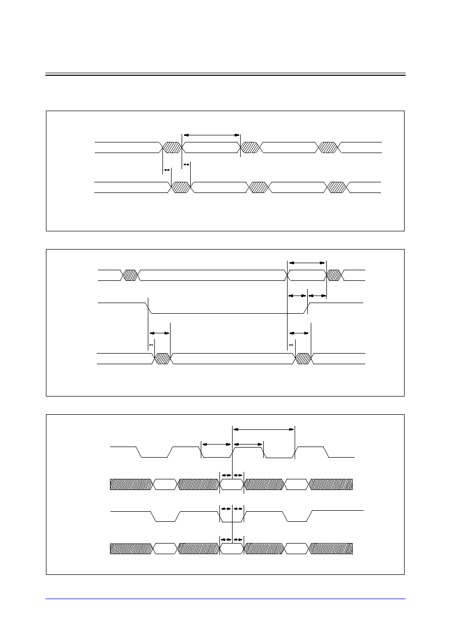
STDL130
5-112
Samsung ASIC
ARFRAM_HDL
High-Density Multi-Port Asynchronous Register File
Timing Diagrams
Read Cycle
Read Cycle with REN-Controlled
Write Cycle
RA[ ]
(OEN = low, REN= low, CK, WEN, DI[ ], WA[ ]= don't care)
t
acc
t
da
DOUT[ ]
t
rcyc
M[A0]
M[A1]
M[A2]
M[A3]
A0
A1
A2
A3
RA [ ]
t
acc
t
da
DOUT [ ]
t
rcyc
DOUT[t-1]
A1
A2
t
acc
t
da
REN
(OEN = low, CK, WEN, DI[ ], WA[ ] = don't care)
DOUT[A1]
DOUT[A2]
t
ras
t
rah
WA
(REN, OEN, RA[ ] = don't care)
t
ckl
t
ckh
t
wcyc
t
was
t
wah
A1
DI [ ]
t
ws
t
wh
t
ds
t
dh
D1
D0
D2
A0
A2
CK
WEN

Samsung ASIC
5-113
STDL130
ARFRAM_HDL
High-Density Multi-Port Asynchronous Register File
OEN Controlled Output Enable
Read-Write Contention
NOTE: If CK rise while WA[] is same as RA[], it is a read-write contention. While CK is high, DOUT[] is UNKNOWN and
write data is valid. After twacc from the falling edge of CK, the read data (D1) is valid.
(CK, REN, WEN, DI[ ], WA[ ], RA[ ] = don't care)
t
od
t
dz
Hi-Z
Valid
OEN
DOUT [ ]
Hi-Z
t
zd
CK< >
(WA[ ] = RA[ ]; WEN, REN, OEN = low)
WA[ ]
A0
A1
A2
t
ckl
t
ckh
t
wcyc
t
was
t
wah
D0
D1
D2
t
ds
t
dh
A1
RA[ ]
DI [ ]
M(A1)
D1
t
wda
t
wacc
DOUT[ ]
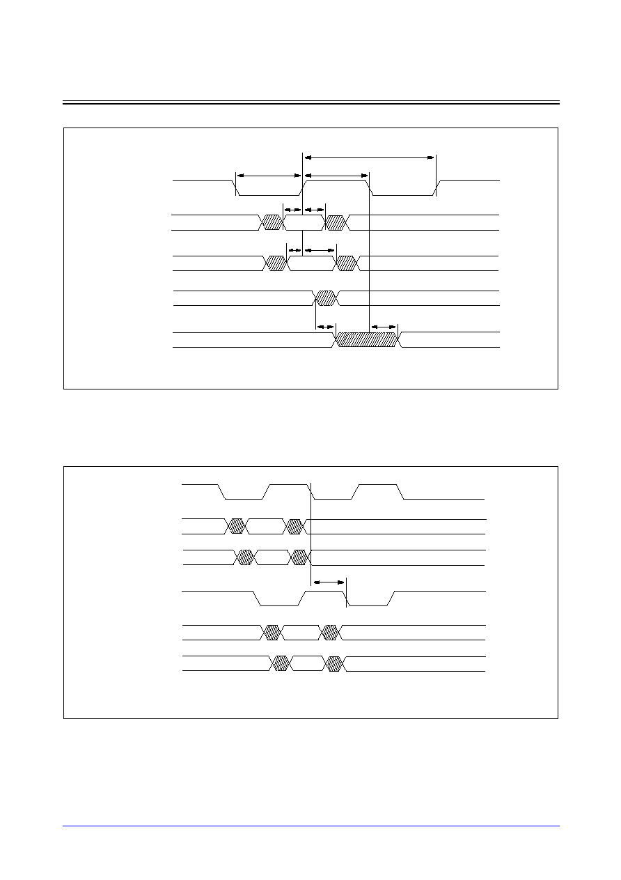
STDL130
5-114
Samsung ASIC
ARFRAM_HDL
High-Density Multi-Port Asynchronous Register File
Write-Read Contention
NOTE: While CK is high, if read access begins by RA<>[] which is same as WA<>[] latched at the rising edge of CK,
it is Write-Read Contention. The read data is invalid whereas the write is still valid. After twacc from the falling
edge of CK, DOUT[] is valid.
Write-Write Contention
NOTES:
1.
If addresses latched at the rising edge of CK are same and t1 is smaller than or equal to twwc, it is Write-Write
Contention. The data stored at current address will be unpredictable.
2.
"don't care" means the condition that these pins are in normal operation mode.
CK< >
(WA[ ] = RA[ ]; WEN, REN, OEN = low)
WA< >[ ]
A0
A1
A2
t
ckl
t
ckh
t
wcyc
t
was
t
wah
D0
D1
D2
t
ds
t
dh
M(A3)
D1
t
wda
t
wacc
A3
DOUT< >[ ]
RA< >[ ]
DI< >[ ]
A1
CK0
(WA0[ ] = WA1[ ]; WEN0, WEN1 = low, OEN, REN, RA[ ] = don't care)
WA0[ ]
A1
WA1[ ]
DI0 [ ]
DI1[ ]
A3
D1
D2
A1
A2
D4
D5
A3
D3
t
l
A0
D0
CK1
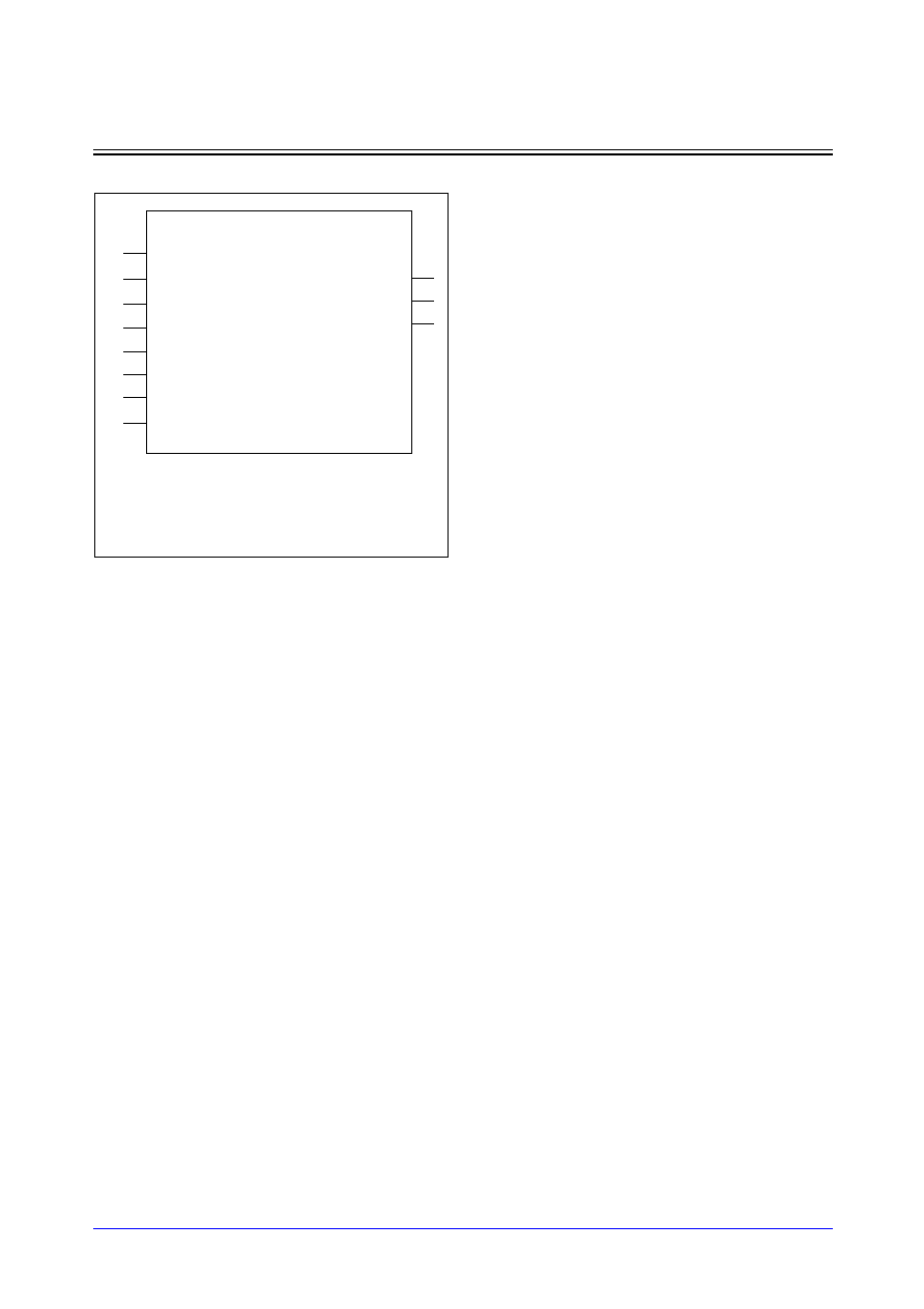
Samsung ASIC
5-115
STDL130
FIFO_HDL
High-Density Synchronous First-In First-Out Memory
Logic Symbol
Function Description
FIFO_HDL is a synchronous first-in first-out buffer memory which is provided as a compiler. FIFO_HDL is
intended for use in high-density applications. After valid reset, on the rising of WCK, the write cycle is
initiated when WEN is low, RST is high and FF is low. The data on DI[] is written into the memory location
specified by the write pointer. During normal write operation, the rising edge of WCK will reset EF if it is set.
At the last available memory location, write operation will set FF. DI[] and WEN must satisfy the setup and
hold requirements with respect to the rising edge of WCK.
On the rising edge of RCK, the read cycle is initiated when REN is low, RST is high, RTM is high and EF is
low. The data located in the memory specified by the read pointer comes in DOUT[] after some delay. During
normal read operation, the rising edge of RCK will reset FF if it is set. At the last available memory location
with available data, read operation will set EF. A valid DOUT[] will be possibly in some specified time after
the rising edge of RCK, under that OEN is low. And the output data will remain unchanged until the next
read, reset, or retransmit mode come in. REN must satisfy the setup and hold requirements with respect to
the rising edge of RCK. When OEN is high, DOUT[] is placed in a high-impedance state.
In reset mode, a reset is globally initiated at the falling edge of RST. The reset operation will set EF and
reset FF and make the data output zero.The reset operation will initiate the read pointer and the write pointer
as 0. After reset operation, the status of EF will make RCK inoperable. The valid write input signal will
become operable as RST is high. The read input signal will remain inoperable until EF is reset by the first
valid write.
In retransmit mode, a retransmit is initiated at the falling edge of RTM only if the total number of writes after
a reset operation is less than the word size of the memory in FIFO_HDL and more than 0 (0 < total number
of write < W-1). The retransmit operation will initiate the read pointer as 0 to allow the retransmission of data,
make DOUT[] zero and make EF reset if it is set. The valid read input signal will become operable as RTM is
high.
Features
∑
Suitable for high-density applications
∑
Over-read and over-write protection capability
∑
Retransmit capability
∑
Synchronous operation
∑
Duty-free clock cycle
∑
Asynchronous tri-state output control
∑
Latched full and empty status flag output
∑
Automatic power-down
∑
Flexible aspect ratio
∑
Up to 64Kbits capacity
∑
Up to 8K number of words
∑
Up to 64 number of bits per word
RCK
OEN
RTM
EF
fifo_hdl_<w>x<b>m<y>
WEN
1. Words(w) is the number of words in FIFO_HDL
2. Bpw(b) is the number of bits per word.
3. Ymux(y) is one of the column mux types.
REN
RST
WCK
NOTES:
DI[b-1:0]
FF
DOUT[b-1:0]
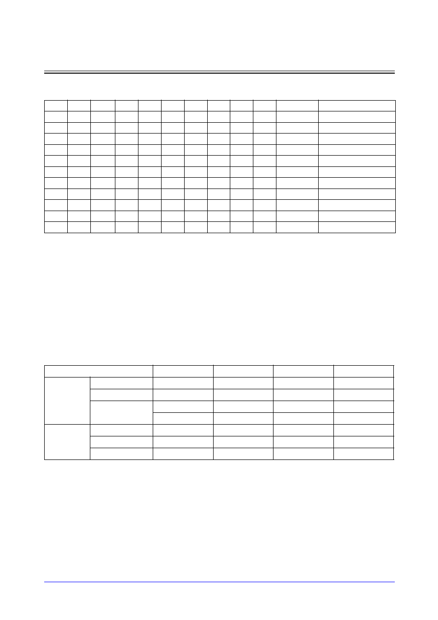
STDL130
5-116
Samsung ASIC
FIFO_HDL
High-Density Synchronous First-In First-Out Memory
FIFO_HDL Function Table
NOTES:
1.
Read is blocked when REN is high and the read port is in disable mode.
2.
Read is blocked when EF is high (overread protection).
3.
Under that OEN is high, DOUT[] goes to tri-state output mode.
4.
Write is blocked when WEN is high and the write port is in disable mode.
5.
Write is blocked when FF is high (overwrite protection).
Parameter Description
FIFO_HDL is the compiler that automatically generates symbol, netlist, timing model, power model and
layout according to the following parameters; Number of words(w), Number of bit per word(b) and Column
mux(y).
RST
WEN
WCK
REN
RCK
RTM
OEN
EF
FF
DI
DOUT
Comment
X
X
X
X
X
X
X
L
Reset mode
H
X
X
X
X
X
X
X
L
Retransmit mode
H
X
X
L
H
L
L
X
DOUT(t)
Read mode
H
L
X
X
X
X
L
Valid
DOUT(t-1)
Write mode
H
X
X
L
H
L
L
X
DOUT(t)
Read and empty mode
H
L
X
X
X
X
L
Valid
DOUT(t-1)
Write and full mode
H
X
X
H
H
L
X
X
X
DOUT(t-1)
(Note 1)
H
X
X
L
H
L
H
X
X
DOUT(t-1)
(Note 2)
X
X
X
X
X
X
H
X
X
X
Hi-Z
(Note 3)
H
H
X
X
X
X
X
X
Valid
DOUT(t-1)
(Note 4)
H
L
X
X
X
X
X
H
Valid
DOUT(t-1)
(Note 5)
Parameters
Ymux(y) = 2
Ymux(y) = 4
Ymux(y) = 8
Ymux(y) = 16
Words (w)
Min
16
32
64
128
Max
1024
2048
4096
8192
Step
w
128:16
w
256:32
w
512:64
w
1024:128
w
>
128:128
w
>
256:256
w
>
512:512
w
>
1024:1024
Bpw (b)
Min
2
2
2
2
Max
64
32
16
8
Step
1
1
1
1
Samsung ASIC
5-117
STDL130
FIFO_HDL
High-Density Synchronous First-In First-Out Memory
Pin Descriptions
Pin Capacitance
(Unit = SL)
Name
I/O
Description
RCK
Read Clock
Read clock input. Upon the rising edge of RCK, it begins a read
operation when REN is low, RST is high, RTM is high and EF is low.
REN
Read Enable
Read enable input. When REN is low, the read access occurs properly.
Conversely when REN is high, no read access can occur and the read
port of the FIFO_HDL goes to power down mode.
REN is latched at the rising edge of RCK.
OEN
Data Output
Enable
Output enable input. The data output enable is asynchronously operated
regardless of the state of other inputs. When OEN is high, DOUT is
disabled and goes to high-impedance state.
RST
Reset
Reset input. Upon the falling edge of RST, the reset mode is initiated.
With reset operation, the read and write pointer goes to their initial
position. Reset operation sets EF and resets FF and makes DOUT[]
zero.
RTM
Retransmit
Retransmit input. Upon the falling edge of RTM, the retransmit mode is
initiated, provided that RST is high. With retransmit operation the read
pointer goes to its initial position. Retransmit operation makes DOUT[]
zero.
WCK
Write Clock
Write clock input. Upon the rising edge of WCK, it begins a write
operation when WE is low, RST is high and FF is low.
WEN
Write Enable
Write enable input. When WEN is low, a write access occurs properly.
Conversely when WEN is high, no write access can occur and the write
port of the FIFO_HDL goes to power down mode. WEN is latched at the
rising edge of WCK.
DI
Data In
Data input bus. DI[] is latched on the rising edge of WCK. Data input is
written into the addressed location in write mode.
EF
Empty Flag
Empty flag. If the memory has no data to be read, EF goes high. Valid
reset makes EF high and valid retransmit makes it low.
FF
Full Flag
Full flag. If the memory has no vacancy to write data, FF goes high.
Valid reset makes FF low.
DOUT
Data Output
Data output bus. Data output is valid after the rising edge of RCK while
the FIFO_HDL is in read mode when OEN is low. Conversely when OEN
is high, DOUT[] goes to high-impedance state. By reset or retransmit
operation. DOUT[] goes to 0.
RST
RTM
WCK
RCK
OEN
WEN
REN
DI
DOUT
7.2222
3.1276
17.7984
9.6708
5.4733
3.6831
3.7654
2.5720
6.8930
STDL130
5-118
Samsung ASIC
FIFO_HDL
High-Density Synchronous First-In First-Out Memory
Block Diagrams
FIFO_HDL supports only 1-bank architecture. The power ports are located on the top-edge and the bottom
edge of both right- and left-sides of the memory. All signal ports are placed at the bottom side of the
memory.
Application Notes
1.
Permitting over-the-cell routing. In chip-level layout, over-the-cell routing in FIFO_HDL is permitted for
Metal-5 layer and Metal-6 layer.
2.
Incoming power bus should be adjusted to guarantee NOT more than 10% voltage drop at typical-case
current levels.
3.
Power stripe should be tapped from both sides of FIFO_HDL.
4.
FIFO_HDL must be reset before any operation performed. The reset operation initiates the read pointer
and the write pointer as 0.
5.
FIFO_HDL should be reset again before resuming normal operation if abnormal operation is performed.
Abnormal operations are invalid retransmit attemption, and read/write operation causing the timing
requirement violations.
6.
The retransmit operation initiates the read pointer as 0.
7.
The retransmit is useful only when the total number of writes after a reset is less than the total word
capacity of the FIFO_HDL and more than 0.
8.
Outputs are not changed until first valid read after a reset or retransmit.
RAM Core
Wr
ite W
ord-line
Shift Register
X-Dec
Read W
ord-line
Shift Register
RAM Core
Y-Dec &
Sense Amp.
Control Block
Y-Dec &
Sense Amp.
I/O Driver
Clock Buffers &
Flag Generator
I/O Driver
VSS
VDD
VDD
VSS
VSS
VDD
VDD
VSS
WEN
RST
FF
DI1[b-1:b/2]
DOUT1[b-1:b/2]
DOUT1[b/2-1:0]
DI1[b/2-1:0]
WCK
EF
REN
RCK
RT
M
OEN

Samsung ASIC
5-119
STDL130
FIFO_HDL
High-Density Synchronous First-In First-Out Memory
Characteristics
Definition for AC Timing (ns)
Symbol
Description
Unit
t
rst
Min RST pulse width low
ns
t
rtm
Min RTM pulse width low
ns
t
rcyc
Read clock cycle time
ns
t
rckh
Read clock pulse width high
ns
t
rckl
Read clock pulse width low
ns
t
wcyc
Write clock cycle time
ns
t
wckh
Write clock pulse width high
ns
t
wckl
Write clock pulse width low
ns
t
rs
REN setup to RCK rising
ns
t
rh
REN hold from RCK rising
ns
t
ws
WEN setup to WCK rising
ns
t
wh
WEN hold from WCK rising
ns
t
wrcs
WCK setup to RCK rising
ns
t
rwcs
RCK setup to WCK rising
ns
t
ds
DI setup to WCK rising
ns
t
dh
DI hold from WCK rising
ns
t
rstw
RST setup to WCK rising
ns
t
rtmr
RTM setup to RCK rising
ns
t
rste
Delay from RST falling to EF rising
ns
t
rstf
Delay from RST falling to FF falling
ns
t
rstd
Delay from RST falling to DOUT zero
ns
t
rstda
Output hold time from RST falling to DOUT
ns
t
rtme
Delay from RTM falling to EF falling
ns
t
rtmd
Delay from RTM falling to DOUT zero
ns
t
rtmda
Output hold time from RTM falling to DOUT
ns
t
we
Delay from WCK rising to EF falling
ns
t
wf
Delay from WCK rising to FF rising
ns
t
rf
Delay from RCK rising to FF falling
ns
t
re
Delay from RCK rising to EF rising
ns
t
acc
Data access time
ns
t
da
De-access time
ns
t
dz
DOUT drive to high-Z time
ns
t
zd
DOUT high-Z to drive time
ns
t
od
OEN to valid output time
ns
Definition for Power Consumption (
µ
W/MHz)
Power_read
The dynamic average power consumption while in a read cycle
uW/MHZ
Power_write
The dynamic average power consumption while in a write cycle
uW/MHZ
Power_w_standby
The write standby power consumption while WEN is high
uW/MHZ
Power_r_standby
The read standby power consumption while REN is high
uW/MHZ
Definition for Area (
µ
m)
Width
The physical width in X-direction
um
Height
The physical height in Y-direction
um

STDL130
5-120
Samsung ASIC
FIFO_HDL
High-Density Synchronous First-In First-Out Memory
Reference Table
* For Ymux=2
(Typical process, 1.8V, 25
∞
C, Output load = 10SL, Input slope = 0.2 ns, SA = 0.5)
Parameters
words
64
128
384
1024
bpw
16
32
48
64
Timing (ns)
t
rst
4.59
4.59
4.60
5.32
t
rtm
4.49
4.49
4.50
5.22
t
rcyc
2.98
3.01
3.05
3.63
t
rckl
0.73
0.73
0.73
0.73
t
rckh
0.40
0.40
0.40
0.40
t
wcyc
2.57
2.62
2.69
3.30
t
wckl
0.83
0.86
0.90
0.93
t
wckh
0.67
0.71
0.75
0.80
t
rs
0.88
0.88
0.88
0.88
t
rh
0.01
0.01
0.01
0.01
t
ws
0.90
0.90
0.90
0.90
t
wh
0.01
0.01
0.01
0.01
t
ds
0.97
0.93
0.90
0.86
t
dh
0.01
0.01
0.01
0.01
t
rstw
0.50
0.50
0.50
0.50
t
rtmr
0.52
0.52
0.52
0.52
t
wrcs
1.30
1.30
1.30
1.30
t
rwcs
1.42
1.41
1.42
1.93
t
rstd
3.38
3.41
3.45
4.20
t
rstda
0.64
0.66
0.68
0.70
t
rste
4.54
4.54
4.55
5.27
t
rstf
4.54
4.54
4.55
5.27
t
rtmd
3.39
3.42
3.45
4.20
t
rtmda
0.65
0.67
0.69
0.71
t
rtme
4.11
4.11
4.11
4.84
t
we
0.90
0.90
0.90
0.90
t
wf
1.94
1.94
1.95
1.95
t
re
1.87
1.87
1.87
1.87
t
rf
0.98
0.98
0.98
0.98
t
acc
2.45
2.48
2.53
3.10
t
da
1.96
2.00
2.02
2.59
t
dz
0.31
0.33
0.35
0.37
t
zd
0.38
0.40
0.42
0.44
t
od
0.66
0.69
0.72
0.75
Power (
µ
W/MHz)
Power_read
57.84
94.57
130.89
181.44
Power_write
56.62
93.78
140.01
223.35
Power_w_standby
2.77
5.11
7.29
9.52
Power_r_standby
0.66
0.73
0.74
0.78
Area (
µ
m)
Width
463.54
636.34
809.14
981.94
Height
244.08
290.16
478.68
949.98
Samsung ASIC
5-121
STDL130
FIFO_HDL
High-Density Synchronous First-In First-Out Memory
Reference Table
* For Ymux=4
(Typical process, 1.8V, 25
∞
C, Output load = 10SL, Input slope = 0.2 ns, SA = 0.5)
Parameters
words
128
256
768
2048
bpw
8
16
24
32
Timing (ns)
t
rst
4.59
4.59
4.61
5.32
t
rtm
4.49
4.49
4.61
5.22
t
rcyc
3.00
3.03
3.08
3.65
t
rckl
0.73
0.73
0.73
0.73
t
rckh
0.40
0.40
0.40
0.40
t
wcyc
2.57
2.62
2.69
3.30
t
wckl
0.82
0.85
0.87
0.89
t
wckh
0.67
0.70
0.72
0.75
t
rs
0.88
0.88
0.88
0.88
t
rh
0.01
0.01
0.01
0.01
t
ws
0.90
0.90
0.90
0.90
t
wh
0.01
0.01
0.01
0.01
t
ds
0.98
0.95
0.93
0.90
t
dh
0.01
0.01
0.01
0.01
t
rstw
0.50
0.50
0.50
0.50
t
rtmr
0.52
0.52
0.52
0.52
t
wrcs
1.30
1.30
1.30
1.30
t
rwcs
1.41
1.41
1.42
1.93
t
rstd
3.44
3.46
3.49
4.23
t
rstda
0.63
0.65
0.66
0.68
t
rste
4.54
4.54
4.56
5.27
t
rstf
4.54
4.54
4.56
5.27
t
rtmd
3.45
3.47
3.49
4.23
t
rtmda
0.64
0.66
0.67
0.69
t
rtme
4.11
4.11
4.12
4.84
t
we
0.90
0.90
0.90
0.90
t
wf
1.94
1.94
1.94
1.95
t
re
1.87
1.87
1.86
1.87
t
rf
0.98
0.98
0.98
0.98
t
acc
2.47
2.50
2.55
3.12
t
da
1.96
2.00
2.02
2.59
t
dz
0.30
0.32
0.33
0.34
t
zd
0.38
0.39
0.41
0.42
t
od
0.65
0.67
0.69
0.71
Power (
µ
W/MHz)
Power_read
53.38
86.40
119.91
165.92
Power_write
50.40
82.12
123.10
200.95
Power_w_standby
1.65
2.84
3.96
5.07
Power_r_standby
0.64
0.66
0.68
0.70
Area (
µ
m)
Width
463.54
636.34
809.14
981.94
Height
244.08
290.16
478.68
949.98

STDL130
5-122
Samsung ASIC
FIFO_HDL
High-Density Synchronous First-In First-Out Memory
Reference Table
* For Ymux=8
(Typical process, 1.8V, 25
∞
C, Output load = 10SL, Input slope = 0.2 ns, SA=0.5)
Parameters
words
256
512
1536
4096
bpw
4
8
12
16
Timing (ns)
t
rst
4.59
4.59
4.60
5.32
t
rtm
4.49
4.49
4.50
5.22
t
rcyc
2.98
3.07
3.11
3.69
t
rckl
0.73
0.73
0.73
0.73
t
rckh
0.40
0.40
0.40
0.40
t
wcyc
2.56
2.62
2.69
3.30
t
wckl
0.81
0.83
0.85
0.87
t
wckh
0.68
0.70
0.72
0.74
t
rs
0.88
0.88
0.88
0.88
t
rh
0.01
0.01
0.01
0.01
t
ws
0.90
0.90
0.90
0.90
t
wh
0.01
0.01
0.01
0.01
t
ds
0.99
0.97
0.95
0.93
t
dh
0.01
0.01
0.01
0.01
t
rstw
0.50
0.50
0.50
0.50
t
rtmr
0.52
0.52
0.52
0.52
t
wrcs
1.30
1.30
1.30
1.30
t
rwcs
1.41
1.41
1.42
1.93
t
rstd
3.57
3.59
3.61
4.35
t
rstda
0.63
0.64
0.65
0.67
t
rste
4.54
4.54
4.55
5.27
t
rstf
4.54
4.54
4.55
5.27
t
rtmd
3.58
3.60
3.61
4.35
t
rtmda
0.64
0.65
0.67
0.68
t
rtme
4.11
4.11
4.11
4.84
t
we
0.90
0.90
0.90
0.90
t
wf
1.94
1.94
1.95
1.95
t
re
1.87
1.87
1.87
1.87
t
rf
0.98
0.98
0.98
0.98
t
acc
2.50
2.54
2.58
3.15
t
da
1.97
2.00
2.02
2.59
t
dz
0.30
0.31
0.32
0.33
t
zd
0.38
0.39
0.40
0.41
t
od
0.64
0.66
0.68
0.70
Power (
µ
W/MHz)
Power_read
51.17
82.31
113.23
158.30
Power_write
47.22
76.34
114.46
189.66
Power_w_standby
1.07
1.73
2.30
2.84
Power_r_standby
0.63
0.64
0.66
0.66
Area (
µ
m)
Width
463.54
636.34
809.14
981.94
Height
244.08
290.16
478.68
949.98

Samsung ASIC
5-123
STDL130
FIFO_HDL
High-Density Synchronous First-In First-Out Memory
Reference Table
* For Ymux=16
(Typical process, 1.8V, 25
∞
C, Output load = 10SL, Input slope = 0.2 ns, SA=0.5)
Parameters
words
512
1024
3072
8192
bpw
2
4
6
8
Timing (ns)
t
rst
4.59
4.59
4.60
5.32
t
rtm
4.49
4.49
4.50
5.22
t
rcyc
3.11
3.14
3.19
3.76
t
rckl
0.73
0.73
0.73
0.73
t
rckh
0.40
0.40
0.40
0.40
t
wcyc
2.56
2.62
2.69
3.30
t
wckl
0.81
0.83
0.84
0.86
t
wckh
0.70
0.72
0.73
0.75
t
rs
0.88
0.88
0.88
0.88
t
rh
0.01
0.01
0.01
0.01
t
ws
0.90
0.90
0.90
0.90
t
wh
0.01
0.01
0.01
0.01
t
ds
0.99
0.97
0.95
0.84
t
dh
0.01
0.01
0.01
0.01
t
rstw
0.50
0.50
0.50
0.50
t
rtmr
0.52
0.52
0.52
0.52
t
wrcs
1.30
1.30
1.30
1.30
t
rwcs
1.40
1.41
1.42
1.93
t
rstd
3.82
3.83
3.85
4.59
t
rstda
0.63
0.64
0.65
0.66
t
rste
4.54
4.54
4.55
5.27
t
rstf
4.54
4.54
4.55
5.27
t
rtmd
3.82
3.84
3.86
4.59
t
rtmda
0.64
0.65
0.66
0.67
t
rtme
4.11
4.11
4.11
4.84
t
we
0.90
0.90
0.90
0.90
t
wf
1.94
1.94
1.95
1.95
t
re
1.87
1.87
1.87
1.87
t
rf
0.98
0.98
0.98
0.98
t
acc
2.57
2.60
2.64
3.22
t
da
1.97
2.00
2.02
2.59
t
dz
0.29
0.31
0.32
0.33
t
zd
0.38
0.39
0.40
0.41
t
od
0.64
0.66
0.67
0.69
Power (
µ
W/MHz)
Power_read
50.01
80.36
110.31
154.37
Power_write
45.11
73.41
110.14
184.08
Power_w_standby
0.61
1.20
1.45
1.71
Power_r_standby
0.61
0.65
0.63
0.61
Area (
µ
m)
Width
463.54
636.34
809.14
981.94
Height
244.08
290.16
478.68
949.98
STDL130
5-124
Samsung ASIC
FIFO_HDL
High-Density Synchronous First-In First-Out Memory
Timing Diagrams
Normal Read Cycle
NOTES:
1.
Read cycle is blocked during empty state (over-read protected)
2.
t
wrcs
is the timing related between first write on empty state and first subsequent read.
If it is not satisfied, DOUT[i] will be unpredictable.
3.
t
re
is the timing related the read and empty mode.
(RST, RTM = high, OEN = low)
t
acc
t
da
DOUT[i-1]
DOUT[i]
t
rs
t
rh
t
rcyc
RCK
t
rckl
t
rckh
t
wrcs
REN
WCK
DOUT
t
rf
FF
t
re
EF
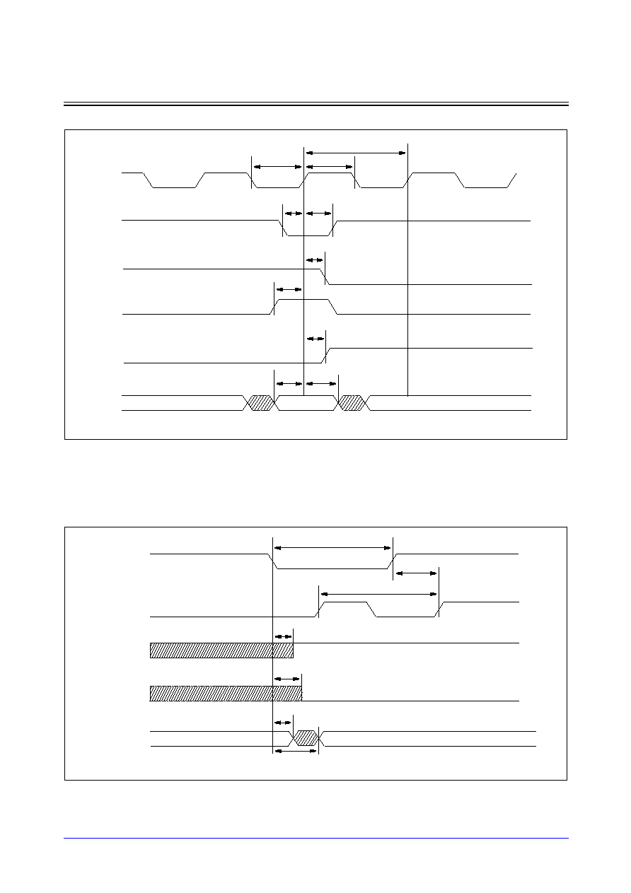
Samsung ASIC
5-125
STDL130
FIFO_HDL
High-Density Synchronous First-In First-Out Memory
Write Cycle
NOTES:
1.
Write cycle is blocked during full state (over-write protected)
2.
t
rwcs
is the timing related between first read on full state and first subsequent write.
If it is not satisfied, DOUT[i] (not shown) will be unpredictable.
3.
t
wf
is the timing related the write and full mode.
Reset Cycle
NOTE: Read cycle and write cycle are blocked when RST is low.
(RST = high)
t
dh
DI[i]
t
ws
t
wh
t
wcyc
WCK
t
wckl
t
wckh
WEN
t
we
EF
DI[]
t
ds
FF
t
rwcs
t
wf
RCK
All 0's
t
rstw
RST
t
rst
WCK, RCK
FF
t
rstf
EF
DOUT
t
rstda
*
NOTE
t
rstd
t
rste
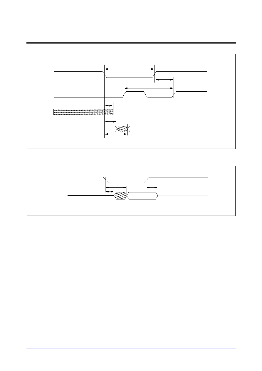
STDL130
5-126
Samsung ASIC
FIFO_HDL
High-Density Synchronous First-In First-Out Memory
Retransmit Cycle
NOTE: Read cycle is blocked when RTM is low.
OEN Controlled Output Enable
All 0's
t
rtmr
RTM
t
rst
t
rtme
RCK
EF
DOUT
*
NOTE
t
rtmda
t
rtmd
t
od
t
dz
Hi-Z
Valid
OEN
DOUT [ ]
Hi-Z
t
zd
(REN = low)
Samsung ASIC
5-127
STDL130
CAM_HDL
High-Density Single-Port Synchronous Binary CAM
Logic Symbol
Function Description
CAM_HDL is a single-port synchronous binary CAM which is provided as a compiler. CAM_HDL is intended
for use in high-density applications. On the rising edge of CK, the write cycle is initiated when WEN is low
and CSN is low and CEN and RN are high. The data on DI[] is written to the addressed CAM location and
VDI overwrites the valid bit associated with CAM entry with the state selected by A[], and DOUT[], VDO,
CAO[] and HIT remains stable during a normal write access cycle. On the rising edge of CK, the read cycle
begins when WEN is high and CSN is low and CEN and RN are high. The data at DOUT[] become valid
after a delay and VDO,during a normal read access cycle, reads back the valid bit associated with the A[]
selected by CAM entry. On the rising edge of CK, the compare cycle starts when CSN and CEN are low and
RN are high, All valid data entries in the CAM are simultaneously searched for the match pattern (CDI[])
defined by mask pattern(CMN[]). CDI[] bits are considered as matched bits at all times, if the corresponding
bits of the applied CMN[] are in low states. Each CAM entry can be excluded from the compare function by
setting the associated valid bit to a low state by the use of VDI. If one or more entries match with the masked
CMN[] pattern, HIT will be asserted and CAO[] will contain the lowest one of all matched addresses by the
built-in priority address encoder. While in standby mode that CSN is high, data stored in the memory is
retained and DOUT[], VDO, CAO[] and HIT remains stable. When OEN is high, DOUT[] and VDO are placed
in a high-impedance state. When AEN is high, CAO[] is placed in a high-impedance state. On the falling
edge of RN, all the valid-bits are invalidated and setted to low states, therefore all the entries are excluded
from CAM match function so no match can occur. A low state of RN inhibits all access, same as when CSN
is in a high state.
Features
∑
Suitable for high-density application
∑
Separated data I/O
∑
Synchronous operation
∑
Duty-free clock cycle
∑
Asynchronous tri-state output control
∑
Latched inputs and outputs
∑
Automatic power-down
∑
Single cycle compare operation
∑
Low noise output optimization
∑
Global hit/miss
∑
Built-in priority address encoder
∑
Asynchronous reset control for all the valid-bits
∑
Up to 32Kbits capacity
∑
Up to 512 number of words
∑
Up to 64 number of bit per word
CK
OEN
AEN
DOUT[b-1:0]
cam_hdl_<w>x<b>m<y>
A[m-1:0]
1. Words(w) is the number of words.
2. Bpw(b) is the number of bits per word.
4. m =
log
2
w
WEN
CEN
CMN[b-1:0]
NOTES:
CSN
DI[b-1:0]
VDI
CDI[b-1:0]
RN
VDO
CAO[m-1:0]
HIT
3. Ymux(y) is one of the column mux types.
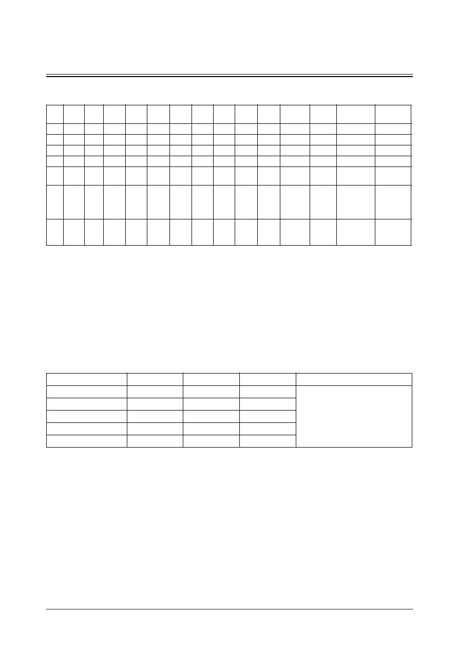
STDL130
5-128
Samsung ASIC
CAM_HDL
High-Density Single-Port Synchronous Binary CAM
CAM_HDL Function Table
NOTES:
1.
DOUT and VDO are high impedance when OEN is high.
2.
CAO is high impedance when AEN is high.
3.
HIT is 1 if matched or 0 if not.
4.
Match pattern is defined by CDI, bit-wise enabled by CMN.
Parameter Description
CAM_HDL is the compiler that automatically generates symbol, netlist, timing model, power model and
layout according to the following parameters; Number of words(w) and Number of bit per word(b) and
column mux(y).
CK
CSN
RN
WEN
AEN
OEN
A
DI/
VDI
CDI
CMN
CEN
DOUT/
VDO
HIT
CAO
Comment
X
X
L
X
L
L
X
X
X
X
X
X
X
X
Reset
X
H
H
X
L
L
X
X
X
X
X
UNCH
UNCH
UNCH
Idle
X
X
X
X
H
H
X
X
X
X
X
Z
UNCH
Z
Tri-state
L
H
L
L
L
Valid
Valid
X
X
H
UNCH
UNCH
UNCH
Write
L
H
H
L
L
Valid
X
X
X
H
Data-
out
UNCH
UNCH
Read
L
H
X
L
L
X
X
Valid
Valid
L
UNCH
1
Lowest of
all
matched
addresses
Matched
compare
cycle
L
H
X
L
L
X
X
Valid
Valid
L
UNCH
0
0
Missed
compare
cycle
Parameters
Min
Max
Step
Note
Address Inputs(m)
3
9
1
Words(w) is limited to one of
(8, 16, 32, 64, 128, 256, 512).
Words (w)
8
512
Note
Bpw (b)
2
64
1
Mux(y)
1
1
-
Capacity
16
32K
-
Samsung ASIC
5-129
STDL130
CAM_HDL
High-Density Single-Port Synchronous Binary CAM
Pin Descriptions
Name
I/O
Description
CK
Clock
Clock input. CSN, WEN, A[], DI[], CDI[], CMN[], VDI and CEN are latched into the CAM on
the rising edge of CK. If CSN and WEN are low and CEN and RN are high on the rising
edge of CK, the CAM is in write mode. If CSN is low and WEN is high and CEN and RN
are high on the rising edge of CK, the CAM is in read mode. If CSN and CEN are low and
RN is high on the rising edge of CK, the CAM is in compare mode.
CSN
Chip Enable
Chip Enable input. The chip enable is active-low and is latched into the CAM on the rising
edge of CK. When CSN is low and RN is high, the CAM is enabled for reading, writing or
comparing, depending on the state of WEN and CEN. When CSN is high and RN is high,
the CAM goes to the standby mode and is disabled for reading or writing or comparing.
DOUT[], VDO, HIT and CAO[] remains previous data output.
WEN
Read/Write
Enable
Read or write enable input. The read/write enable is latched into the CAM on the rising
edge of CK depending on the state of CEN. When CSN and WEN is low and CEN and RN
are high, data are written to the addressed location and DOUT[], VDO, HIT and CAO[]
remains stable. When CSN is low and WEN is high and CEN and RN are high, data from
the addressed word are present at DOUT[] and VDO, whereas HIT and CAO[] remains
stable.
OEN
Data Output
Enable
Data output enable input. The data output enable is asynchronously operated regardless
of any input. When OEN is high, DOUT[] and VDO are disabled and go to high-impedance
state.
CEN
Compare Enable
Compare enable input. The compare enable is latched into the CAM on the rising edge of
CK. When CSN and CEN is low and RN is high, the CAM match function is activated.
When CSN is low and CEN and RN are high, only read-write accesses are permitted.
AEN
Address Output
Enable
Address output enable input. The address output enable is asynchronously operated
regardless of any input. When AEN is high, CAO[] is disabled and goes to high-impedance
state.
CMN [ ]
Compare Mask
Input
Compare mask input bus. CMN[] defines the pattern which enables the CDI[] pattern to be
used for the CAM match function. If the CMN[] bit is low, the corresponding CDI[] bit will be
interpreted as a wild card.
A [ ]
Address
Address input bus. The address is latched into the CAM on the rising edge of CK.
DI [ ]
Data Input
Data input bus. Data are latched on the rising edge of CK. Data input is written into the
addressed location in write mode.
VDI
Valid Bit Input
Valid Bit Input. VDI overwrites the valid bit associated with the CAM entry with the state
selected by A[], during a normal write access cycle. Valid Bit Input are latched on the rising
edge of CK.
CDI [ ]
Compare Data
Input
Compare Data input bus. Compare-data are latched on the rising edge of CK and define
the data pattern to be matched with the CAM entries, in conjunction to CMN[].
RN
Reset Enable
Reset Enable. RN, if low, invalidates all the CAM entries by setting all the valid-bits, one
per entry,to low states,therefore all the entries are excluded from CAM match function so
no match can occur. A low state of RN inhibits all access, same as when CSN is in a high
state.
DOUT [ ]
Data Output
Data output bus. Data output is valid after the rising edge of CK while the CAM is in read
mode. Data output remains previous data output while the CAM is in write mode and
compare mode.
VDO
Valid Bit Output
Valid bit output. VDO, during a normal read access cycle, reads back the valid bit
associated with the A[] selected by CAM entry.
CAO [ ]
Address Output
Address output bus. CAO[] presents the address of the matched entry, in a single match
case. In a multiple-match case, CAO[] is the lowest one of all matched addresses by the
built-in priority address encoder.
HIT
Match Output
Match Output. HIT indicates one or more CAM entries matched the masked CDI[], if high.
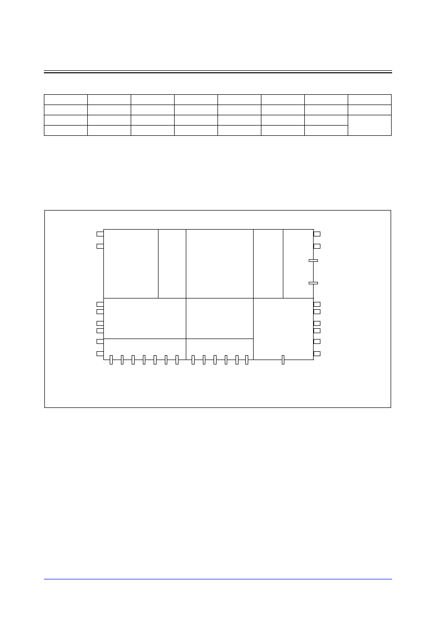
STDL130
5-130
Samsung ASIC
CAM_HDL
High-Density Single-Port Synchronous Binary CAM
Pin Capacitance
(Unit = SL)
Block Diagrams
CAM_HDL supports only 1-bank architecture. The power ports are located on the top-edge and the bottom
edge of both right- and left-sides of the memory. All signal ports except HIT and CAO are located on the
bottom of the memory. HIT and CAO are located on the right-edge of the memory.
CK
CSN
WEN
OEN
CEN
AEN
CMN
A
4.5580
0.7506
1.5115
0.7506
1.5115
1.6233
1.5115
1.5115
DI
VDI
CDI
RN
DOUT
CDO
CAO
1.5115
1.5115
1.5115
0.7506
17.7912
17.7912
17.7912
X-Dec
W
ord-line
Decoder
RAM Core
Pr
ior
ity Address
encoder
I/O Dr
iv
er
Control Block
Y-Dec & Sense Amp.
Matched Address
Control Block
Address & Clock Buffers
I/O Driver
VSS
VDD
VDD
VSS
VSS
VDD
VDD
VSS
OEN
CEN
VDO
AEN
CSN
A[]
WEN
VDI
DOUT[]
DI[]
CDI[]
CMN[]
RN
CK
HIT
CAO[]
VSS
VDD
VSS
VDD
VSS
VDD
VSS
VDD

Samsung ASIC
5-131
STDL130
CAM_HDL
High-Density Single-Port Synchronous Binary CAM
Application Notes
1.
Permitting over-the-cell routing. In chip-level layout, over-the-cell routing in CAM_HDL is permitted only
for Metal-5 layer or upper layers.
2.
Incoming power bus should be adjusted to guarantee NOT more than 10% voltage drop at typical-case
current levels.
3.
Power stripe should be tapped from both sides of CAM_HDL.
4.
Power reduction during standby mode. The standby power is measured on the condition that only CSN
is disable mode and other signals are in operation mode. If any of signals are activated while in standby
mode, the power will be consumed because the input switching activities are occurred by the signal
transition. Therefore, to reduce unnecessary power consumption, you should keep stable for all signals
while in standby mode.
STDL130
5-132
Samsung ASIC
CAM_HDL
High-Density Single-Port Synchronous Binary CAM
Characteristics
Definition for AC Timing (ns)
Symbol
Description
Symbol
Description
t
cyc
Clock cycle time
t
da
De-access time
t
ckl
Clock pulse width low
t
vdacc
Validity data access time
t
ckh
Clock pulse width high
t
vdda
Validity data de-access time
t
as
Address setup time
t
caacc
Matched address access time
t
ah
Address hold time
t
cada
Matched address de-access time
t
cs
CSN setup time
t
htacc
Global Hit/Miss access time
t
ch
CSN hold time
t
htda
Global Hit/Miss de-access time
t
ds
Data-In setup time
t
dz
DOUT drive to high-Z time
t
dh
Data-In hold time
t
zd
DOUT high-Z to drive time
t
ws
WEN setup time
t
od
OEN to valid output time
t
wh
WEN hold time
t
vddz
VDO drive to high-Z time
t
ces
CEN setup time
t
vdzd
VDO high-Z to drive time
t
ceh
CEN hold time
t
vdod
OEN to valid output time for VDO
t
cms
CMN setup time
t
cadz
CAO drive to high-Z time
t
cmh
CMN hold time
t
cazd
CAO high-Z to drive time
t
vds
VDI setup time
t
caod
AEN to valid output time for CAO
t
vdh
VDI hold time
t
rn
Min RN pulse width low
t
cds
CDI setup time
t
rns
RN setup time
t
cdh
CDI hold time
t
rnh
RN hold time
t
acc
Data access time
Definition for Power Consumption (
µ
W/MHz)
Power_read
The dynamic average power consumption while in a read cycle
Power_write
The dynamic average power consumption while in a write cycle
Power_compare
The dynamic average power consumption while in a compare cycle
Power_reset
The dynamic average power consumption while in a reset mode
Power_standby
The standby power consumption while CSN and RN are high, OEN and AEN are low
and other signals are in normal operations
Definition for Area (
µ
m)
Width
The physical width in X-direction
Height
The physical height in Y-direction

Samsung ASIC
5-133
STDL130
CAM_HDL
High-Density Single-Port Synchronous Binary CAM
Reference Table
* For Ymux=1
(Typical process, 1.8V, 25
∞
C, Output load = 10SL, Input slope = 0.2 ns, SA = 0.5)
Parametersy
words
16
32
64
128
256
512
bpw
8
8
8
8
8
8
Timing (ns)
t
cyc
4.10
4.15
4.25
5.39
6.69
8.21
t
ckl
1.03
1.05
1.07
1.09
1.10
1.12
t
ckh
1.10
1.10
1.10
1.10
1.10
1.10
t
as
0.35
0.35
0.35
0.35
0.35
0.35
t
ah
0.34
0.37
0.40
0.44
0.47
0.50
t
cs
1.03
1.05
1.07
1.09
1.10
1.12
t
ch
0.69
0.69
0.69
0.69
0.69
0.69
t
ces
0.55
0.57
0.59
0.61
0.62
0.64
t
ceh
0.69
0.69
0.69
0.69
0.69
0.69
t
cms
0.34
0.34
0.34
0.34
0.34
0.34
t
cmh
0.41
0.41
0.41
0.41
0.41
0.41
t
ds
0.34
0.34
0.34
0.34
0.34
0.34
t
dh
0.45
0.45
0.45
0.45
0.45
0.45
t
vds
0.34
0.34
0.34
0.34
0.34
0.34
t
vdh
0.45
0.45
0.45
0.45
0.45
0.45
t
cds
0.34
0.34
0.34
0.34
0.34
0.34
t
cdh
0.41
0.41
0.41
0.41
0.41
0.41
t
ws
0.28
0.28
0.28
0.28
0.28
0.28
t
wh
0.34
0.37
0.40
0.44
0.47
0.50
t
acc
2.02
2.07
2.16
2.32
2.63
3.26
t
da
1.77
1.82
1.91
2.07
2.38
3.01
t
dz
0.48
0.48
0.48
0.48
0.48
0.48
t
zd
0.61
0.61
0.61
0.61
0.61
0.61
t
od
0.69
0.69
0.69
0.69
0.69
0.69
t
vdacc
2.02
2.07
2.16
2.32
2.63
3.26
t
vdda
1.77
1.82
1.91
2.07
2.38
3.01
t
vddz
0.48
0.48
0.48
0.48
0.48
0.48
t
vdzd
0.61
0.61
0.61
0.61
0.61
0.61
t
vdod
0.69
0.69
0.69
0.69
0.69
0.69
t
caacc
3.22
3.36
3.74
4.43
5.46
6.69
t
cada
2.09
2.16
2.29
2.84
3.51
4.35
t
cadz
0.42
0.45
0.48
0.55
0.68
0.96
t
cazd
0.60
0.62
0.65
0.71
0.83
1.09
t
caod
0.68
0.70
0.73
0.79
0.90
1.16
t
htacc
2.90
3.12
3.40
4.11
4.94
5.92
t
htda
2.09
2.16
2.29
2.84
3.51
4.35
t
rn
3.30
3.35
3.45
4.59
5.89
7.41
t
rns
1.03
1.05
1.07
1.09
1.10
1.12
t
rnh
3.30
3.35
3.45
4.09
5.89
7.41
Power (
µ
W/MHz)
Power_read
20.36
22.92
26.45
32.57
45.09
72.44
Power_write
18.96
22.13
27.87
39.33
63.17
108.83
Power_compare
68.00
78.54
94.38
125.18
180.78
283.36
Power_standby
0.46
0.50
0.59
0.66
0.79
1.08
Power_reset
1.25
2.02
3.50
6.79
14.83
36.56
Area (
µ
m)
Width
210.48
232.12
253.76
275.40
297.06
318.70
Height
382.08
455.04
600.96
892.80
1476.48
2643.84
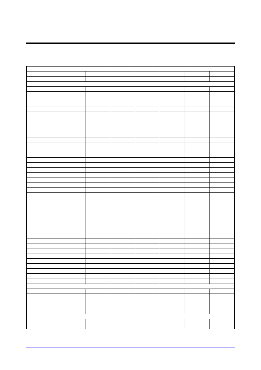
STDL130
5-134
Samsung ASIC
CAM_HDL
High-Density Single-Port Synchronous Binary CAM
Reference Table
* For Ymux=1
(Typical process, 1.8V, 25
∞
C, Output load = 10SL, Input slope = 0.2 ns, SA = 0.5)
Parameters
words
16
32
64
128
256
512
bpw
16
16
16
16
16
16
Timing (ns)
t
cyc
4.41
4.46
4.56
5.69
7.01
8.56
t
ckl
1.03
1.05
1.07
1.09
1.10
1.12
t
ckh
1.10
1.10
1.10
1.10
1.10
1.10
t
as
0.35
0.35
0.35
0.35
0.35
0.35
t
ah
0.34
0.37
0.40
0.44
0.47
0.50
t
cs
1.03
1.05
1.07
1.09
1.10
1.12
t
ch
0.69
0.69
0.69
0.69
0.69
0.69
t
ces
0.55
0.57
0.59
0.61
0.62
0.64
t
ceh
0.69
0.69
0.69
0.69
0.69
0.69
t
cms
0.34
0.34
0.34
0.34
0.34
0.34
t
cmh
0.45
0.45
0.45
0.45
0.45
0.45
t
ds
0.34
0.34
0.34
0.34
0.34
0.34
t
dh
0.49
0.49
0.49
0.49
0.49
0.49
t
vds
0.34
0.34
0.34
0.34
0.34
0.34
t
vdh
0.49
0.49
0.49
0.49
0.49
0.49
t
cds
0.34
0.34
0.34
0.34
0.34
0.34
t
cdh
0.45
0.45
0.45
0.45
0.45
0.45
t
ws
0.28
0.28
0.28
0.28
0.28
0.28
t
wh
0.34
0.37
0.40
0.44
0.47
0.50
t
acc
2.10
2.15
2.24
2.41
2.72
3.35
t
da
1.85
1.90
1.99
2.16
2.47
3.10
t
dz
0.53
0.53
0.53
0.53
0.53
0.53
t
zd
0.65
0.65
0.65
0.65
0.65
0.65
t
od
0.73
0.73
0.73
0.73
0.73
0.73
t
vdacc
2.10
2.15
2.24
2.41
2.72
3.35
t
vdda
1.85
1.90
1.99
2.16
2.47
3.10
t
vddz
0.53
0.53
0.53
0.53
0.53
0.53
t
vdzd
0.65
0.65
0.65
0.65
0.65
0.65
t
vdod
0.73
0.73
0.73
0.73
0.73
0.73
t
caacc
3.44
3.57
3.96
4.64
5.68
6.94
t
cada
2.30
2.37
2.51
3.06
3.74
4.63
t
cadz
0.43
0.45
0.48
0.55
0.68
0.96
t
cazd
0.60
0.62
0.65
0.71
0.83
1.09
t
caod
0.68
0.70
0.73
0.79
0.90
1.17
t
htacc
3.11
3.33
3.62
4.32
5.16
6.18
t
htda
2.30
2.37
2.51
3.06
3.74
4.63
t
rn
3.61
3.66
3.76
4.89
6.21
7.76
t
rns
1.03
1.05
1.07
1.09
1.10
1.12
t
rnh
3.61
3.66
3.76
4.89
6.21
7.76
Power (
µ
W/MHz)
Power_read
28.68
31.93
35.93
42.70
56.11
85.40
Power_write
26.05
30.39
38.43
54.50
88.27
151.22
Power_compare
104.19
117.94
140.05
183.33
263.20
410.25
Power_standby
0.58
0.61
0.75
0.83
1.01
1.42
Power_reset
1.25
2.04
3.51
6.85
14.87
36.67
Area (
µ
m)
Width
255.44
277.08
298.72
320.36
342.02
363.66
Height
382.08
455.04
600.96
892.80
1476.48
2643.84

Samsung ASIC
5-135
STDL130
CAM_HDL
High-Density Single-Port Synchronous Binary CAM
Reference Table
* For Ymux=1
(Typical process, 1.8V, 25
∞
C, Output load = 10SL, Input slope = 0.2 ns, SA = 0.5)
Parameters
words
16
32
64
128
256
512
bpw
32
32
32
32
32
32
Timing (ns)
t
cyc
4.94
4.99
5.10
6.24
7.57
9.18
t
ckl
1.03
1.05
1.07
1.09
1.10
1.12
t
ckh
1.10
1.10
1.10
1.10
1.10
1.10
t
as
0.35
0.35
0.35
0.35
0.35
0.35
t
ah
0.34
0.37
0.40
0.44
0.47
0.50
t
cs
1.03
1.05
1.07
1.09
1.10
1.12
t
ch
0.69
0.69
0.69
0.69
0.69
0.69
t
ces
0.55
0.57
0.59
0.61
0.62
0.64
t
ceh
0.69
0.69
0.69
0.69
0.69
0.69
t
cms
0.34
0.34
0.34
0.34
0.34
0.34
t
cmh
0.53
0.53
0.53
0.53
0.53
0.53
t
ds
0.34
0.34
0.34
0.34
0.34
0.34
t
dh
0.57
0.57
0.57
0.57
0.57
0.57
t
vds
0.34
0.34
0.34
0.34
0.34
0.34
t
vdh
0.57
0.57
0.57
0.57
0.57
0.57
t
cds
0.34
0.34
0.34
0.34
0.34
0.34
t
cdh
0.53
0.53
0.53
0.53
0.53
0.53
t
ws
0.28
0.28
0.28
0.28
0.28
0.28
t
wh
0.34
0.37
0.40
0.44
0.47
0.50
t
acc
2.24
2.29
2.39
2.56
2.28
3.51
t
da
1.99
2.04
2.14
2.31
2.63
3.26
t
dz
0.62
0.62
0.62
0.62
0.62
0.62
t
zd
0.73
0.73
0.73
0.73
0.73
0.73
t
od
0.81
0.81
0.81
0.81
0.81
0.81
t
vdacc
2.24
2.29
2.39
2.56
2.88
3.51
t
vdda
1.99
2.04
2.14
2.31
2.63
3.26
t
vddz
0.62
0.62
0.62
0.62
0.62
0.62
t
vdzd
0.73
0.73
0.73
0.73
0.73
0.73
t
vdod
0.81
0.81
0.81
0.81
0.81
0.81
t
caacc
3.80
3.93
4.33
5.02
6.08
7.37
t
cada
2.65
2.73
2.87
3.42
4.13
5.05
t
cadz
0.43
0.45
0.48
0.55
0.68
0.96
t
cazd
0.60
0.62
0.65
0.71
0.83
1.09
t
caod
0.68
0.70
0.73
0.79
0.90
1.16
t
htacc
3.47
3.69
4.00
4.70
5.55
6.61
t
htda
2.65
2.73
2.87
3.42
4.13
5.05
t
rn
4.14
4.19
4.30
5.44
6.77
8.38
t
rns
1.03
1.05
1.07
1.09
1.10
1.12
t
rnh
4.14
4.19
4.30
5.44
6.77
8.38
Power (
µ
W/MHz)
Power_read
45.34
50.06
55.14
62.83
78.54
112.32
Power_write
40.34
46.85
59.49
84.80
138.41
236.40
Power_compare
176.44
196.41
231.07
299.13
427.57
663.65
Power_standby
0.82
0.90
0.96
1.15
1.51
2.18
Power_reset
1.26
2.05
3.54
6.90
14.97
36.87
Area (
µ
m)
Width
345.36
367.00
388.64
410.28
431.94
453.58
Height
382.08
455.04
600.96
892.80
1476.48
2643.84

STDL130
5-136
Samsung ASIC
CAM_HDL
High-Density Single-Port Synchronous Binary CAM
Reference Table
* For Ymux=1
(Typical process, 1.8V, 25
∞
C, Output load = 10SL, Input slope = 0.2 ns, SA = 0.5)
Parameters
words
16
32
64
128
256
512
bpw
64
64
64
64
64
64
Timing (ns)
t
cyc
5.92
5.98
6.11
7.25
8.65
10.35
t
ckl
1.03
1.05
1.07
1.09
1.10
1.12
t
ckh
1.10
1.10
1.10
1.10
1.10
1.10
t
as
0.35
0.35
0.35
0.35
0.35
0.35
t
ah
0.34
0.37
0.40
0.44
0.47
0.50
t
cs
1.03
1.05
1.07
1.09
1.10
1.12
t
ch
0.69
0.69
0.69
0.69
0.69
0.69
t
ces
0.55
0.57
0.59
0.61
0.63
0.65
t
ceh
0.69
0.69
0.69
0.69
0.69
0.69
t
cms
0.34
0.34
0.34
0.34
0.34
0.34
t
cmh
0.68
0.68
0.68
0.68
0.68
0.68
t
ds
0.34
0.34
0.34
0.34
0.34
0.34
t
dh
0.72
0.72
0.72
0.72
0.72
0.72
t
vds
0.34
0.34
0.34
0.34
0.34
0.34
t
vdh
0.72
0.72
0.72
0.72
0.72
0.72
t
cds
0.34
0.34
0.34
0.34
0.34
0.34
t
cdh
0.68
0.68
0.68
0.68
0.68
0.68
t
ws
0.28
0.28
0.28
0.28
0.28
0.28
t
wh
0.34
0.37
0.40
0.44
0.47
0.50
t
acc
2.50
2.56
2.66
2.85
3.18
3.83
t
da
2.25
2.31
2.41
2.60
2.93
3.58
t
dz
0.80
0.80
0.80
0.80
0.80
0.80
t
zd
0.87
0.87
0.87
0.87
0.87
0.87
t
od
0.94
0.94
0.94
0.94
0.94
0.94
t
vdacc
2.50
2.56
2.66
2.85
3.18
3.83
t
vdda
2.25
2.31
2.41
2.60
2.93
3.58
t
vddz
0.80
0.80
0.80
0.80
0.80
0.80
t
vdzd
0.87
0.87
0.87
0.87
0.87
0.87
t
vdod
0.94
0.94
0.94
0.94
0.94
0.94
t
caacc
4.43
4.58
4.98
5.68
6.79
8.21
t
cada
3.28
3.36
3.53
4.09
4.84
5.89
t
cadz
0.43
0.45
0.48
0.55
0.68
0.96
t
cazd
0.60
0.62
0.65
0.71
0.83
1.09
t
caod
0.68
0.70
0.73
0.79
0.90
1.16
t
htacc
4.11
4.34
4.65
5.39
6.27
7.45
t
htda
3.28
3.36
3.53
4.09
4.84
5.89
t
rn
5.12
5.18
5.31
6.45
7.85
9.55
t
rns
1.03
1.05
1.07
1.09
1.10
1.12
t
rnh
5.12
5.18
5.31
6.45
7.85
9.55
Power (
µ
W/MHz)
Power_read
79.34
86.71
94.31
104.44
124.72
167.22
Power_write
89.60
80.93
102.71
146.63
239.39
408.82
Power_compare
326.04
356.24
414.41
531.58
757.32
1167.60
Power_standby
1.34
1.38
1.66
1.89
2.49
3.71
Power_reset
1.28
2.08
3.60
6.94
15.24
37.28
Area (
µ
m)
Width
525.20
546.84
568.48
590.12
611.78
633.42
Height
382.08
455.04
600.96
892.80
1476.48
2643.84
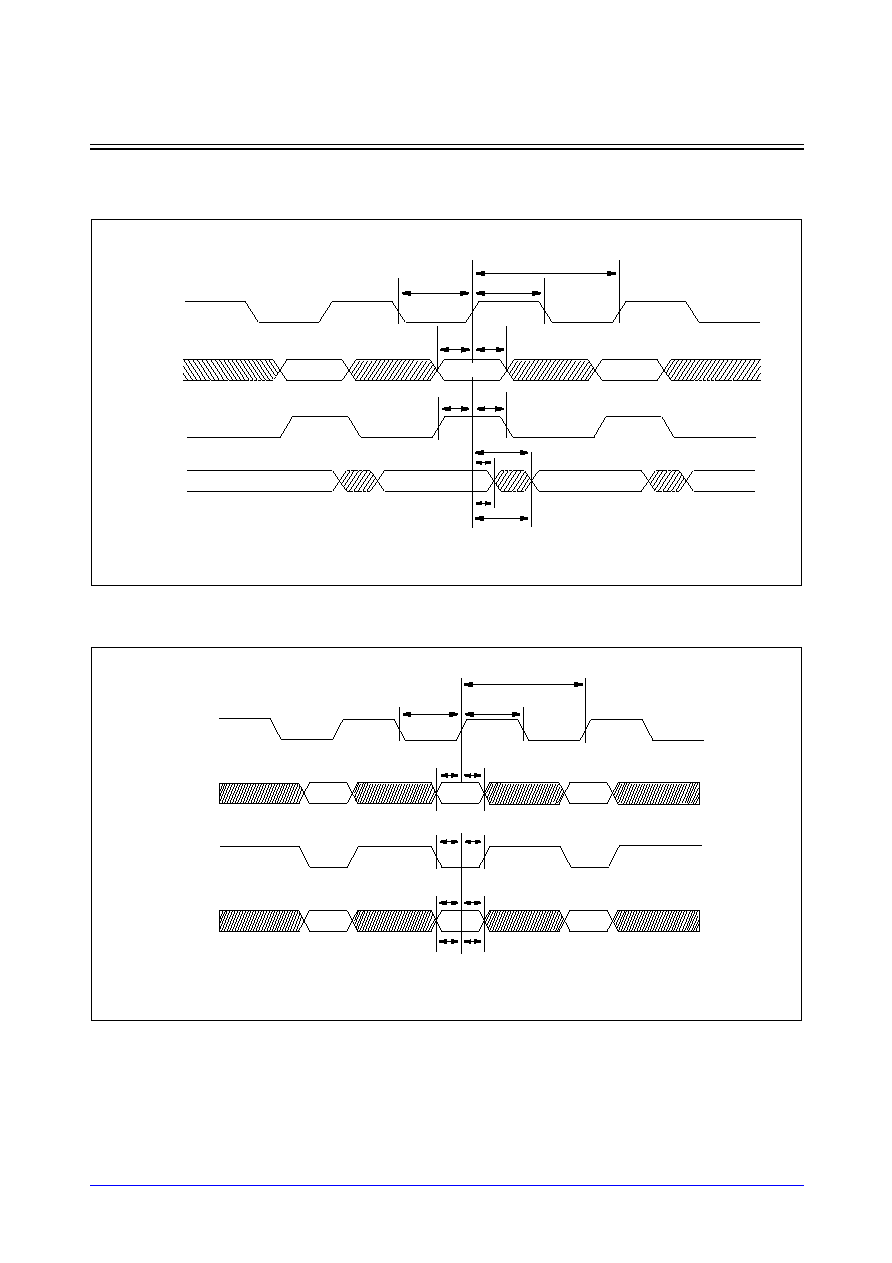
Samsung ASIC
5-137
STDL130
CAM_HDL
High-Density Single-Port Synchronous Binary CAM
Timing Diagrams
Read Cycle
Write Cycle
t
as
A
t
ah
(RN=high, CSN=low, OEN=low, CEN=high, AEN, DI, VDI, CDI, CMN= don't care)
t
acc
WEN
t
ws
t
wh
t
da
DOUT/VDO
t
cyc
CK
t
ckl
t
ckh
A0
A2
Valid
M[A0]
M[A1]
M[A2]
A1
t
vdda
t
vdacc
A
(RN = high, CSN = low, CEN = high, OEN, AEN, CDI, CMN = don't care)
t
ckl
t
ckh
t
cyc
t
as
t
ah
A1
DI/VDI
t
ws
t
wh
t
ds
t
dh
D1
D0
D2
A0
A2
CK
WEN
t
vds
t
vdh
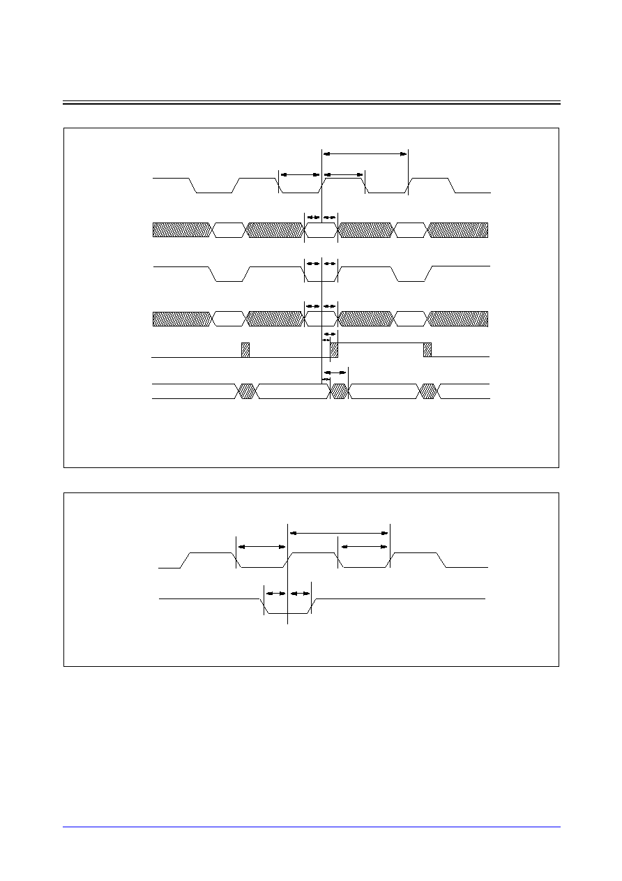
STDL130
5-138
Samsung ASIC
CAM_HDL
High-Density Single-Port Synchronous Binary CAM
Compare Cycle
CSN Controlled
CMN
(RN = high, CSN = low, A, WEN, OEN, AEN = don't care)
t
ckl
t
ckh
t
cyc
t
cms
t
cmh
M1
CDI
t
ces
t
ceh
t
cds
t
cdh
D1
D0
D2
M0
M2
CK
CEN
t
caacc
Unknown
A(M[D1])
t
htacc
t
htda
t
cada
0
0
HIT
CAO
Miss Cycle
Miss Cycle
Hit Cycle
(RN, WEN, OEN CEN, AEN, A, DI, VDI, CDI, CMN = valid)
CSN
t
cs
t
ch
t
cyc
CK
t
ckl
t
ckh
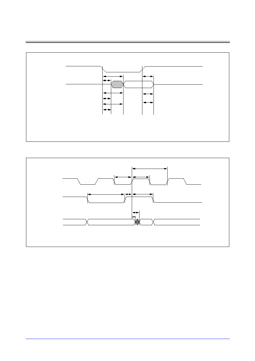
Samsung ASIC
5-139
STDL130
CAM_HDL
High-Density Single-Port Synchronous Binary CAM
OEN/AEN Controlled Output Enable
NOTE: "don't care" means the condition that these pins are in normal operation mode.
RN Controlled Reset Mode
(RN, CK, CSN, WEN, CEN, AEN, CMN, A, DI, VDI, CDI = don't care)
t
od
t
dz
Hi-Z
Valid
OEN/AEN
DOUT/VDO/CAO
Hi-Z
t
zd
t
vdod
t
caod
t
vdzd
t
cazd
t
vddz
t
cadz
RN
(OEN, CSN, WEN, CEN, AEN, CMN, A, DI, VDI, CDI = valid)
t
ckl
t
ckh
t
cyc
t
rns
t
rnh
t
caacc/
t
htacc
Valid
CK
DOUT/VDO
t
rn
t
acc/
t
vdacc
t
da/
t
vdda
t
cada/
t
htda
Valid
X
X
CAO/HIT
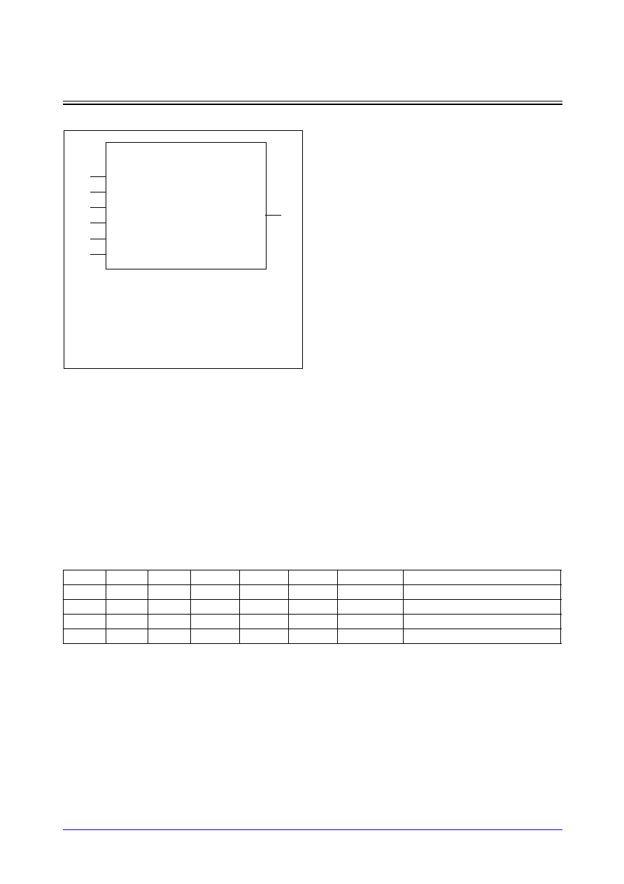
Samsung ASIC
5-141
STDL130
SPSRAM_LPL
Low-Power Single-Port Synchronous Static RAM
Logic Symbol
Function Description
SPSRAM_LPL is a single-port synchronous static RAM which is provided as a compiler. SPSRAM_LPL is
intended for use in Low-Power applications. On the rising edge of CK, the write cycle is initiated when WEN
is low and CSN is low. The data on DI[] is written into the memory location specified on A[]. During the write
cycle, DOUT[] remains stable. On the rising edge of CK, the read cycle is initiated when WEN is high and
CSN is low. The data at DOUT[] become valid after a delay. While in standby mode that CSN is high, data
stored in the memory is retained and DOUT[] remains stable. When OEN is high, DOUT[] is placed in a
high-impedance state.
SPSRAM_LPL Function Table
CK
CSN
WEN
OEN
A
DI
DOUT
Comment
X
X
X
H
X
X
Z
Unconditional tri-state output
X
H
X
L
X
X
DOUT(t-1)
De-selected (standby mode)
L
L
L
Valid
Valid
DOUT(t-1)
Write cycle
L
H
L
Valid
X
MEM(A)
Read cycle
CK
CSN
WEN
OEN
A [m-1:0]
spsram_lpl_<w>x<b>m<y>
DOUT [b≠1:0]
DI [b≠1:0]
NOTES:
1. Words(w) is the number of words.
2. Bpw(b) is the number of bits per word.
3. Ymux(y) is one of the column mux types.
4. m =
log
2
w
Features
∑
Suitable for low-power application
∑
Separated data I/O
∑
Synchronous operation
∑
Duty-free clock cycle
∑
Asynchronous tri-state output control
∑
Latched inputs and outputs
∑
Automatic power-down
∑
Zero standby current
∑
Zero hold time
∑
Low noise output optimization
∑
Flexible aspect ratio
∑
Up to 512Kbits capacity
∑
Up to 16K number of words
∑
Up to 256 number of bits per word
STDL130
5-142
Samsung ASIC
SPSRAM_LPL
Low-Power Single-Port Synchronous Static RAM
Parameter Description
SPSRAM_LPL is the compiler that automatically generates symbol, netlist, timing model, power model and
layout according to the following parameters; Number of words(w), Number of bit per word(b), Column
mux(y).
Pin Descriptions
Pin Capacitance
Unit: [SL]
NOTE: Each pin's capacitance is exactly same regardless of available mux types.
Parameters
Ymux(y) = 4
Ymux(y) = 8
Ymux(y) = 16
Ymux(y) = 32
Words (w)
Min
64
128
256
512
Max
4096
8192
16384
32768
Step
32
64
128
256
Bpw (b)
Min
1
1
1
1
Max
128
64
32
16
Step
1
1
1
1
Name
I/O
Description
CK
Clock
Clock input. CSN, WEN, A[] and DI[] are latched into the RAM on the rising
edge of CK. If CSN and WEN are low on the rising edge of CK, the RAM is in
write mode. If WEN is high on the rising edge of CK, the RAM is in read mode.
Upon the falling edge of CK, the RAM is in a precharge state.
CSN
Chip
Enable
Chip enable input. The chip enable is active-low and is latched into the RAM on
the rising edge of CK. When CSN is low, the RAM is enabled for reading or
writing, depending on the state of WEN. When CSN is high, the RAM goes to
the standby mode and is disabled for reading or writing. DOUT remains
previous data output.
WEN
Read/Write
Enable
Read or write enable input. The read/write enable is latched into the RAM on
the rising edge of CK. When WEN is low, data are written to the addressed
location and DOUT remains stable. When WEN is high, data from the
addressed word are present at DOUT.
OEN
Data
Output
Enable
Data output enable input. The data output enable is asynchronously operated
regardless of the state of other input. When OEN is high, DOUT is disabled and
goes to high-impedance state.
A [ ]
Address
Address input bus. The address is latched into the RAM on the rising edge of
CK.
DI [ ]
Data Input
Data input bus. Data are latched on the rising edge of CK. Data input is written
into the addressed location in write mode.
DOUT [ ]
Data
Output
Data output bus. Data output is valid after the rising edge of CK while the RAM
is in read mode. Data output remains previous data output while the RAM is in
write mode.
CK
CSN
WEN
OEN
A
DI
DOUT
12.39
3.56
4.43
6.12
4.43
4.84
10.81
Samsung ASIC
5-143
STDL130
SPSRAM_LPL
Low-Power Single-Port Synchronous Static RAM
Block Diagrams
SPSRAM_LPL supports only 1-bank architecture. The power ports are located on the middle-edge and the
bottom edge of both right- and left-sides of the memory. All signal ports are only located on the bottom sides
of the memory.
Application Notes
1.
Permitting over-the-cell routing.
In chip-level layout, over-the-cell routing in SPSRAM_LPL is permitted only for Metal-5 and Metal-6
layers. Incoming power bus should be adjusted to guarantee NOT more than 10% voltage drop at
typical-case current levels.
2.
Incoming power bus should be adjusted to guarantee NOT more than 10% voltage drop at typical-case
current levels.
3.
Power stripe should be tapped from both sides of SPSRAM_LPL.
4.
Power reduction during standby mode.
The standby power is measured on the condition that only CSN is disable mode and other signals are in
operation mode except that OEN is tied to low. If any of signals are activated while in standby mode, the
power will be consumed because the input switching activities are occurred by the signal transition.
Therefore, to reduce unnecessary power consumption, you should keep stable for all signals while in
standby mode
RAM Core
W
ord-line Decoder
X-Dec
W
ord-line Decoder
RAM Core
Y-Dec &
Sense Amp.
Control Block
Y-Dec &
Sense Amp.
I/O Driver
Address &
Clock Buffers
I/O Driver
VDD
VSS
VDD
VSS
VDD
VSS
VDD
VSS
DOUT[b-1:b/2]
DI[b-1:b/2]
A[m-1:0]
WEN
OEN
CSN
CK
DOUT[b/2-1:0]
DI[b/2-1:0]
STDL130
5-144
Samsung ASIC
SPSRAM_LPL
Low-Power Single-Port Synchronous Static RAM
Characteristics
Definition for AC Timing (ns)
Symbol
Description
Symbol
Description
t
cyc
Clock cycle time
t
ckh
Clock pulse width high
t
ckl
Clock pulse width low
t
as
Address setup time
t
ah
Address hold time
t
cs
CSN setup time
t
ch
CSN hold time
t
ds
Data-In setup time
t
dh
Data-In hold time
t
ws
WEN setup time
t
wh
WEN hold time
t
acc
Data access time
t
da
De-access time
t
dz
DOUT drive to high-Z time
t
zd
DOUT high-Z to drive time
t
od
OEN to valid output time
Definition for Power Consumption (
µ
W/MHz)
Power_read
The dynamic average power consumption while in a read cycle
Power_write
The dynamic average power consumption while in a write cycle
Power_standby
The standby power consumption while CSN is high, OEN is low and other signals are in
normal operation
Definition for Area (
µ
m)
Width
The physical width in X-direction
Height
The physical height in Y-direction

Samsung ASIC
5-145
STDL130
SPSRAM_LPL
Low-Power Single-Port Synchronous Static RAM
Reference Table
* For Ymux=4
(Typical process, 1.8V, 25
∞
C, Output load = 10SL, Input slope = 0.2 ns, SA=0.5)
NOTE: Standby power is measured on the condition that other signals are in normal operation while CSN is in disable
mode and OEN is low
.
Parameters
words
64
128
256
512
1024
2048
3072
4096
bpw
16
32
48
64
80
96
112
128
Timing (ns)
t
cyc
3.56
3.58
3.60
3.64
3.68
4.16
4.66
5.34
t
ckl
1.09
1.09
1.09
1.09
1.09
1.09
1.09
1.09
t
ckh
1.15
1.15
1.15
1.15
1.15
1.15
1.15
1.15
t
as
0.30
0.30
0.30
0.30
0.30
0.30
0.30
0.30
t
ah
0.01
0.01
0.01
0.01
0.01
0.01
0.01
0.01
t
cs
0.40
0.40
0.40
0.40
0.40
0.40
0.40
0.40
t
ch
0.01
0.01
0.01
0.01
0.01
0.01
0.01
0.01
t
ds
0.53
0.51
0.50
0.48
0.46
0.45
0.43
0.41
t
dh
0.01
0.01
0.01
0.01
0.01
0.01
0.01
0.01
t
ws
0.57
0.57
0.57
0.57
0.57
0.57
0.57
0.57
t
wh
0.01
0.01
0.01
0.01
0.01
0.01
0.01
0.01
t
acc
3.46
3.48
3.50
3.54
3.58
4.06
4.56
5.26
t
da
3.10
3.12
3.14
3.16
3.19
3.67
4.17
4.87
t
dz
0.65
0.67
0.70
0.72
0.75
0.77
0.79
0.82
t
zd
0.75
0.77
0.80
0.82
0.85
0.87
0.89
0.92
t
od
0.85
0.87
0.90
0.92
0.95
0.97
0.99
1.02
Power (
µ
W/MHz)
Power_read
41.81
56.69
73.96
96.82
132.41
168.35
201.82
233.59
Power_write
51.75
73.42
97.06
125.30
163.97
205.76
244.72
289.53
Power_standby
2.70
4.66
6.64
8.66
10.76
12.92
15.71
22.23
Area (
µ
m)
Width
219.89
338.46
457.02
575.58
694.15
812.71
931.28
1049.84
Height
207.04
248.51
331.44
497.32
829.06
1504.82
2180.58
2856.34

STDL130
5-146
Samsung ASIC
SPSRAM_LPL
Low-Power Single-Port Synchronous Static RAM
Reference Table
* For Ymux=8
(Typical process, 1.8V, 25
∞
C, Output load = 10SL, Input slope = 0.2 ns, SA=0.5)
NOTE: Standby power is measured on the condition that other signals are in normal operation while CSN is in disable
mode and OEN is low
.
Parameters
words
128
256
512
1024
2048
4096
6144
8192
bpw
8
16
24
32
40
48
56
64
Timing (ns)
t
cyc
3.61
3.62
3.64
3.66
3.69
4.17
4.68
5.36
t
ckl
1.09
1.09
1.09
1.09
1.09
1.09
1.09
1.09
t
ckh
1.15
1.15
1.15
1.15
1.15
1.15
1.15
1.15
t
as
0.30
0.30
0.30
0.30
0.30
0.30
0.30
0.30
t
ah
0.01
0.01
0.01
0.01
0.01
0.01
0.01
0.01
t
cs
0.40
0.40
0.40
0.40
0.40
0.40
0.40
0.40
t
ch
0.01
0.01
0.01
0.01
0.01
0.01
0.01
0.01
t
ds
0.53
0.52
0.51
0.50
0.48
0.47
0.46
0.44
t
dh
0.01
0.01
0.01
0.01
0.01
0.01
0.01
0.01
t
ws
0.57
0.57
0.57
0.57
0.57
0.57
0.57
0.57
t
wh
0.01
0.01
0.01
0.01
0.01
0.01
0.01
0.01
t
acc
3.51
3.52
3.54
3.56
3.59
4.07
4.58
5.26
t
da
3.11
3.13
3.14
3.16
3.19
3.68
4.18
4.87
t
dz
0.64
0.66
0.68
0.69
0.71
0.73
0.74
0.76
t
zd
0.74
0.76
0.78
0.79
0.81
0.83
0.84
0.86
t
od
0.84
0.86
0.88
0.89
0.91
0.93
0.94
0.96
Power (
µ
W/MHz)
Power_read
41.21
55.53
72.27
94.66
129.92
164.69
195.65
225.76
Power_write
50.03
67.86
87.75
112.44
148.11
185.25
219.89
265.01
Power_standby
1.77
2.76
3.77
4.84
6.02
6.99
8.33
13.37
Area (
µ
m)
Width
219.71
338.30
456.89
575.48
694.07
812.66
931.25
1049.84
Height
207.04
248.51
331.44
497.32
829.06
1504.82
2180.58
2856.34

Samsung ASIC
5-147
STDL130
SPSRAM_LPL
Low-Power Single-Port Synchronous Static RAM
Reference Table
* For Ymux=16
(Typical process, 1.8V, 25
∞
C, Output load = 10SL, Input slope = 0.2 ns, SA=0.5)
NOTE: Standby power is measured on the condition that other signals are in normal operation while CSN is in disable
mode and OEN is low
.
Parameters
words
256
512
1024
2048
4096
8192
12288
16384
bpw
4
8
12
16
20
24
28
32
Timing (ns)
t
cyc
3.64
3.66
3.68
3.70
3.73
4.20
4.71
5.39
t
ckl
1.09
1.09
1.09
1.09
1.09
1.09
1.09
1.09
t
ckh
1.15
1.15
1.15
1.15
1.15
1.15
1.15
1.15
t
as
0.30
0.30
0.30
0.30
0.30
0.30
0.30
0.30
t
ah
0.01
0.01
0.01
0.01
0.01
0.01
0.01
0.01
t
cs
0.40
0.40
0.40
0.40
0.40
0.40
0.40
0.40
t
ch
0.01
0.01
0.01
0.01
0.01
0.01
0.01
0.01
t
ds
0.53
0.52
0.51
0.50
0.49
0.48
0.48
0.46
t
dh
0.01
0.01
0.01
0.01
0.01
0.01
0.01
0.01
t
ws
0.57
0.57
0.57
0.57
0.57
0.57
0.57
0.57
t
wh
0.01
0.01
0.01
0.01
0.01
0.01
0.01
0.01
t
acc
3.54
3.56
3.57
3.60
3.62
4.11
4.61
5.30
t
da
3.14
3.16
3.18
3.21
3.24
3.71
4.22
4.91
t
dz
0.64
0.65
0.67
0.68
0.69
0.70
0.72
0.73
t
zd
0.74
0.75
0.77
0.78
0.79
0.80
0.82
0.83
t
od
0.84
0.85
0.87
0.88
0.89
0.90
0.92
0.93
Power (
µ
W/MHz)
Power_read
41.05
55.03
71.47
93.64
128.85
162.32
193.02
222.07
Power_write
48.51
64.49
82.51
105.29
138.92
174.79
205.90
251.95
Power_standby
1.24
1.76
2.28
2.82
3.41
4.27
5.22
8.83
Area (
µ
m)
Width
219.32
337.97
456.61
575.26
693.90
812.55
931.19
1049.84
Height
207.04
248.51
331.44
497.32
829.06
1504.82
2180.58
2856.34

STDL130
5-148
Samsung ASIC
SPSRAM_LPL
Low-Power Single-Port Synchronous Static RAM
Reference Table
* For Ymux=32
(Typical process, 1.8V, 25
∞
C, Output load = 10SL, Input slope = 0.2 ns, SA=0.5)
NOTE: Standby power is measured on the condition that other signals are in normal operation while CSN is in disable
mode and OEN is low
.
Parameters
words
512
1024
2048
4096
8192
16384
24576
32768
bpw
2
4
6
8
10
12
14
16
Timing (ns)
t
cyc
3.69
3.71
3.73
3.76
3.79
4.26
4.77
5.45
t
ckl
1.10
1.09
1.09
1.09
1.09
1.09
1.09
1.09
t
ckh
1.15
1.15
1.15
1.15
1.15
1.15
1.15
1.15
t
as
0.30
0.30
0.30
0.30
0.30
0.30
0.30
0.30
t
ah
0.01
0.01
0.01
0.01
0.01
0.01
0.01
0.01
t
cs
0.40
0.40
0.40
0.40
0.40
0.40
0.40
0.40
t
ch
0.01
0.01
0.01
0.01
0.01
0.01
0.01
0.01
t
ds
0.51
0.50
0.48
0.47
0.45
0.44
0.42
0.41
t
dh
0.01
0.01
0.01
0.01
0.01
0.01
0.01
0.01
t
ws
0.57
0.57
0.57
0.57
0.57
0.57
0.57
0.57
t
wh
0.01
0.01
0.01
0.01
0.01
0.01
0.01
0.01
t
acc
3.59
3.61
3.63
3.66
3.69
4.16
4.67
5.35
t
da
3.19
3.21
3.23
3.25
3.29
3.77
4.28
4.98
t
dz
0.66
0.68
0.71
0.73
0.75
0.77
0.80
0.82
t
zd
0.76
0.78
0.81
0.83
0.85
0.87
0.90
0.92
t
od
0.86
0.88
0.91
0.93
0.95
0.97
1.00
1.02
Power (
µ
W/MHz)
Power_read
41.19
54.99
71.27
93.28
128.38
161.44
191.46
220.11
Power_write
48.41
63.64
80.90
102.90
135.73
169.20
201.68
246.47
Power_standby
0.99
1.28
1.58
1.91
2.29
2.68
3.21
7.04
Area (
µ
m)
Width
218.52
337.28
456.04
574.80
693.56
812.32
931.08
1049.84
Height
207.04
248.51
331.44
497.32
829.06
1504.82
2180.58
2856.34
Samsung ASIC
5-149
STDL130
SPSRAM_LPL
Low-Power Single-Port Synchronous Static RAM
Timing Diagrams
Read Cycle
Write Cycle
t
as
A [ ]
t
ah
(CSN = low, OEN = low, DI = don't care)
t
acc
WEN
t
ws
t
wh
t
da
DOUT [ ]
t
cyc
CK
t
ckl
t
ckh
A0
A2
Valid
M[A0]
M[A1]
M[A2]
A1
t
as
A [ ]
t
ah
(CSN = low, OEN = don't care)
WEN
t
ws
t
wh
DI [ ]
t
cyc
CK
t
ckl
t
ckh
A0
A2
A1
t
ds
t
dh
D0
D2
D1

STDL130
5-150
Samsung ASIC
SPSRAM_LPL
Low-Power Single-Port Synchronous Static RAM
Read Cycle with CSN Controlled
OEN Controlled Output Enable
NOTE: "don't care" means the condition that these pins are in normal operation mode.
t
as
A [ ]
t
ah
(OEN = low, WEN = high, DI = don't care)
CSN
t
cs
t
ch
DOUT [ ]
t
cyc
CK
t
ckl
t
ckh
A0
A2
A1
t
da
t
acc
M(A1)
M(A0)
(CK, A, WEN, DI, CSN = don't care)
t
od
t
dz
Hi-Z
Valid
OEN
DOUT [ ]
Hi-Z
t
zd
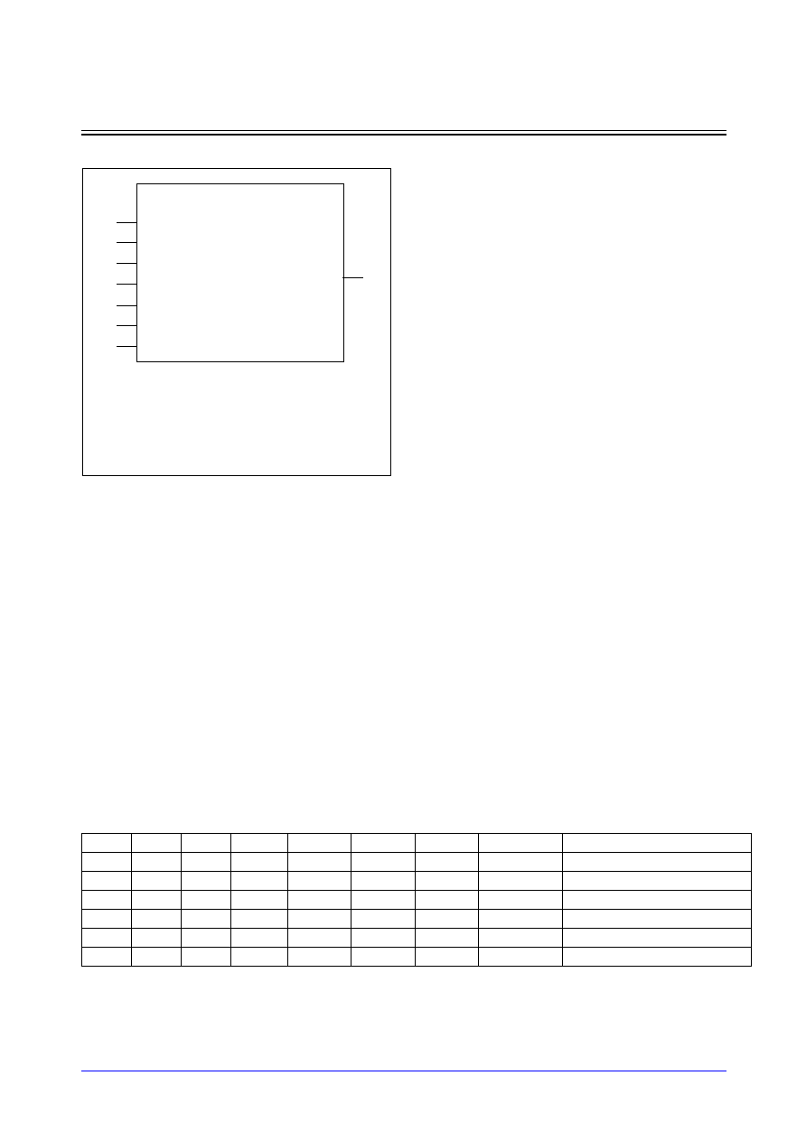
Samsung ASIC
5-151
STDL130
SPSRAMBW_LPL
Low-Power Single-Port Synchronous Static RAM with Bit-Write
Logic Symbol
Function Description
SPSRAMBW_LPL is a single-port synchronous static RAM with bit-write capability which is provided as a
compiler. SPSRAMBW_LPL is intended for use in Low-Power applications. Basically, its functionality is
exactly same as SPSRAM_LPL except a bit-write operation which is controlled by BWEN[], named bit-write
enable signal bus. Each bit of BWEN[] enables or disable the write operation of its corresponding bit in DI[].
On the rising edge of CK, the write cycle is initiated when WEN is low and CSN is low. The data bytes or bits
in DI[], which their corresponding bit(s) in BWEN[] are low, are written into the memory location specified on
A[]. When all bits of BWEN[] are high, any data in DI[] are not written into the memory location specified on
A[]. When all bits of BWEN[] are low, the data in DI[] are written into the memory location specified on A[],
which is exactly same as the write operation in SPSRAM_LPL. During the write cycle, DOUT[] remains
stable. On the rising edge of CK, the read cycle is initiated when WEN is high and CSN is low. The data at
DOUT[] become valid after a delay. While in standby mode that CSN is high, A[] and DI[] are disabled, data
stored in the memory is retained and DOUT[] remains stable. When OEN is high, DOUT[] is placed in a
high-impedance state.
SPSRAMBW_LPL Function Table
CK
CSN
WEN
OEN
A
BWEN
DI
DOUT
Comment
X
X
X
H
X
X
X
Z
Unconditional tri-state output
X
H
X
L
X
X
X
DOUT(t-1)
De-selected (standby mode)
L
L
L
Valid
all L
Valid
DOUT(t-1)
Word-write cycle
L
L
L
Valid
L
Valid
DOUT(t-1)
Bit-write cycle
L
L
L
Valid
all H
Valid
DOUT(t-1)
No operation
L
H
L
Valid
X
X
MEM(A)
Read cycle
Features
∑
Suitable for low-power application
∑
Bit-write capability
∑
Separated data I/O
∑
Synchronous operation
∑
Duty-free clock cycle
∑
Asynchronous tri-state output control
∑
Latched inputs and outputs
∑
Automatic power-down
∑
Zero standby current
∑
Zero hold time
∑
Low noise output optimization
∑
Flexible aspect ratio
∑
Up to 512Kbits capacity
∑
Up to 16K number of words
∑
Up to 256 number of bits per word
CK
CSN
WEN
OEN
A [m-1:0]
spsrambw_lpl_<w>x<b>m<y>
DOUT [b≠1:0]
DI [b≠1:0]
NOTES:
1. Words(w) is the number of words.
2. Bpw(b) is the number of bits per word.
3. Ymux(y) is one of the column mux types.
4. m =
log
2
w
BWEN[b-1:0]
STDL130
5-152
Samsung ASIC
SPSRAMBW_LPL
Low-Power Single-Port Synchronous Static RAM with Bit-Write
Parameter Description
SPSRAMBW_LPL is the compiler that automatically generates symbol, netlist, timing model, power model
and layout according to the following parameters; Number of words(w), Number of bit per word(b) and
Column mux(y).
Pin Descriptions
Parameters
Ymux(y) = 4
Ymux(y) = 8
Ymux(y) = 16
Ymux(y) = 32
Words (w)
Min
64
128
256
512
Max
4096
8192
16384
32768
Step
32
64
128
256
Bpw (b)
Min
1
1
1
1
Max
128
64
32
16
Step
1
1
1
1
Name
I/O
Description
CK
Clock
Clock input. CSN, WEN, A[] and DI[] are latched into the RAM on the rising
edge of CK. If CSN and WEN are low on the rising edge of CK, the RAM is in
write mode. If WEN is high on the rising edge of CK, the RAM is in read mode.
Upon the falling edge of CK, the RAM is in a precharge state.
CSN
Chip
Enable
Chip Enable input. The chip enable is active-low and is latched into the RAM
on the rising edge of CK. When CSN is low, the RAM is enabled for reading or
writing, depending on the state of WEN. When CSN is high, the RAM goes to
the standby mode and is disabled for reading or writing. DOUT remains
previous data output.
WEN
Read/Write
Enable
Read or write enable input. The read/write enable is latched into the RAM on
the rising edge of CK. When WEN is low, data are written to the addressed
location and DOUT remains stable. When WEN is high, data from the
addressed word are present at DOUT.
BWEN [ ]
Bit-Write
Enable
Bit-write enable input bus. The bit-write enable is latched into the RAM on the
rising edge of CK. Each bit of BWEN[] enables/disables the write operation of
corresponding data bit. BWEN[i] corresponds to DI[i] in bit-write. If WEN and
BWEN[0] are low and BWEN[1] is high, DI[0] is written into the memory
location specified on A[], but DI[1] is not written.
OEN
Data
Output
Enable
Data output enable input. The data output enable is asynchronously operated
regardless of the state of other input. When OEN is high, DOUT is disabled
and goes to high-impedance state.
A [ ]
Address
Address input bus. The address is latched into the RAM on the rising edge of
CK.
DI [ ]
Data Input
Data input bus. Data are latched on the rising edge of CK. Data input is written
into the addressed location in write mode.
DOUT [ ]
Data
Output
Data output bus. Data output is valid after the rising edge of CK while the RAM
is in read mode. Data output remains previous data output while the RAM is in
write mode.
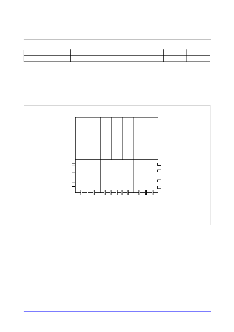
Samsung ASIC
5-153
STDL130
SPSRAMBW_LPL
Low-Power Single-Port Synchronous Static RAM with Bit-Write
Pin Capacitance
Unit: [SL]
NOTE: Each pin's capacitance is exactly same regardless of available mux types.
Block Diagrams
SPSRAMBW_LPL supports only 1-bank architecture. The power ports are located on the middle-edge and
the bottom edge of both right- and left-sides of the memory. All signal ports are only located on the bottom
sides of the memory.
CK
CSN
WEN
BWEN
OEN
A
DI
DOUT
12.39
3.56
4.43
4.84
6.12
4.43
4.84
10.81
RAM Core
W
ord-line Decoder
X-Dec
W
ord-line Decoder
RAM Core
Y-Dec &
Sense Amp.
Control Block
Y-Dec &
Sense Amp.
I/O Driver
Address &
Clock Buffers
I/O Driver
VDD
VSS
VDD
VSS
VDD
VSS
VDD
VSS
DOUT[b-1:b/2]
DI[b-1:b/2]
A[m-1:0]
WEN
OEN
CSN
CK
DOUT[b/2-1:0]
DI[b/2-1:0]
BWEN[b-1:b/2]
BWEN[b/2-1:0]]

STDL130
5-154
Samsung ASIC
SPSRAMBW_LPL
Low-Power Single-Port Synchronous Static RAM with Bit-Write
Application Notes
1.
Permitting over-the-cell routing.
In chip-level layout, over-the-cell routing in SPSRAMBW_LPL is permitted for only Metal-5 and Metal-6
layers.
2.
Incoming power bus should be adjusted to guarantee NOT more than 10% voltage drop at typical-case
current levels.
3.
Power stripe should be tapped from both sides of SPSRAMBW_LPL.
4.
A byte-write or word-write operation with SPSRAMBW_LPL.
Refer to the function table. In byte-write operation, the number of BWEN[] signal bus should be divided
by a byte (8) and eight BWEN signals should be tied to a connection wire. In this case, DI[] bus is
controlled by a byte-wired BWEN signal instead of each BWEN bit. In word-write operation, the
functionality is exactly same as SPSRAM_LPL. If all of BWEN[] signal is tied to low state, DI[] bus is
only controlled by WEN.
5.
Power reduction during standby mode.
The standby power is measured on the condition that only CSN is disable mode and other signals are in
operation mode except that OEN is tied to low. If any of signals are activated while in standby mode, the
power will be consumed because the input switching activities are occurred by the signal transition.
Therefore, to reduce unnecessary power consumption, you should keep stable for all signals while in
standby mode.
Samsung ASIC
5-155
STDL130
SPSRAMBW_LPL
Low-Power Single-Port Synchronous Static RAM with Bit-Write
Characteristics
Definition for AC Timing (ns)
Symbol
Description
Symbol
Description
t
cyc
Clock cycle time
t
ckh
Clock pulse width high
t
ckl
Clock pulse width low
t
as
Address setup time
t
ah
Address hold time
t
cs
CSN setup time
t
ch
CSN hold time
t
ds
Data-In setup time
t
dh
Data-In hold time
t
ws
WEN setup time
t
wh
WEN hold time
t
acc
Data access time
t
bwh
BWEN hold time
t
bws
BWEN setup time
t
da
De-access time
t
dz
DOUT drive to high-Z time
t
zd
DOUT high-Z to drive time
t
od
OEN to valid output time
Definition for Power Consumption (
µ
W/MHz)
Power_read
The dynamic average power consumption while in a read cycle
Power_write
The dynamic average power consumption while in a write cycle
Power_standby
The standby power consumption while CSN is high, OEN is low and other signals are in
normal operation
Definition for Area (
µ
m)
Width
The physical width in X-direction
Height
The physical height in Y-direction
STDL130
5-156
Samsung ASIC
SPSRAMBW_LPL
Low-Power Single-Port Synchronous Static RAM with Bit-Write
Reference Table
* For Ymux=4
(Typical process, 1.8V, 25
∞
C, Output load = 10SL, Input slope = 0.2 ns, SA=0.5)
NOTE: Standby power is measured on the condition that other signals are in normal operation while CSN is in disable
mode and OEN is low
.
Parameters
words
64
128
256
512
1024
2048
3072
4096
bpw
16
32
48
64
80
96
112
128
Timing (ns)
t
cyc
3.56
3.58
3.60
3.64
3.68
4.16
4.66
5.34
t
ckl
1.09
1.09
1.09
1.09
1.09
1.09
1.09
1.09
t
ckh
1.15
1.15
1.15
1.15
1.15
1.15
1.15
1.15
t
as
0.30
0.30
0.30
0.30
0.30
0.30
0.30
0.30
t
ah
0.01
0.01
0.01
0.01
0.01
0.01
0.01
0.01
t
cs
0.40
0.40
0.40
0.40
0.40
0.40
0.40
0.40
t
ch
0.01
0.01
0.01
0.01
0.01
0.01
0.01
0.01
t
ds
0.53
0.51
0.50
0.48
0.46
0.45
0.43
0.41
t
dh
0.01
0.01
0.01
0.01
0.01
0.01
0.01
0.01
t
ws
0.57
0.57
0.57
0.57
0.57
0.57
0.57
0.57
t
wh
0.01
0.01
0.01
0.01
0.01
0.01
0.01
0.01
t
bws
0.48
0.46
0.45
0.43
0.41
0.40
0.38
0.36
t
bwh
0.01
0.01
0.01
0.01
0.01
0.01
0.01
0.01
t
acc
3.46
3.48
3.50
3.54
3.58
4.06
4.56
5.26
t
da
3.10
3.12
3.14
3.16
3.19
3.67
4.17
4.87
t
dz
0.65
0.67
0.70
0.72
0.75
0.77
0.79
0.82
t
zd
0.75
0.77
0.80
0.82
0.85
0.87
0.89
0.92
t
od
0.85
0.87
0.90
0.92
0.95
0.97
0.99
1.02
Power (
µ
W/MHz)
Power_read
41.81
56.69
73.96
96.82
132.41
168.35
201.82
233.59
Power_write
53.48
76.69
102.41
132.44
172.92
216.54
257.26
303.94
Power_standby
4.40
8.20
11.98
15.80
19.70
23.70
28.25
36.64
Area (
µ
m)
Width
219.89
338.46
457.02
575.58
694.15
812.71
931.28
1049.84
Height
207.04
248.51
331.44
497.32
829.06
1504.82
2180.58
2856.34
Samsung ASIC
5-157
STDL130
SPSRAMBW_LPL
Low-Power Single-Port Synchronous Static RAM with Bit-Write
Reference Table
* For Ymux=8
(Typical process, 1.8V, 25
∞
C, Output load = 10SL, Input slope = 0.2 ns, SA=0.5)
NOTE: Standby power is measured on the condition that other signals are in normal operation while CSN is in disable
mode and OEN is low
.
Parameters
words
128
256
512
1024
2048
4096
6144
8192
bpw
8
16
24
32
40
48
56
64
Timing (ns)
t
cyc
3.61
3.62
3.64
3.66
3.69
4.17
4.68
5.36
t
ckl
1.09
1.09
1.09
1.09
1.09
1.09
1.09
1.09
t
ckh
1.15
1.15
1.15
1.15
1.15
1.15
1.15
1.15
t
as
0.30
0.30
0.30
0.30
0.30
0.30
0.30
0.30
t
ah
0.01
0.01
0.01
0.01
0.01
0.01
0.01
0.01
t
cs
0.40
0.40
0.40
0.40
0.40
0.40
0.40
0.40
t
ch
0.01
0.01
0.01
0.01
0.01
0.01
0.01
0.01
t
ds
0.53
0.52
0.51
0.50
0.48
0.47
0.46
0.44
t
dh
0.01
0.01
0.01
0.01
0.01
0.01
0.01
0.01
t
ws
0.57
0.57
0.57
0.57
0.57
0.57
0.57
0.57
t
wh
0.01
0.01
0.01
0.01
0.01
0.01
0.01
0.01
t
bws
0.48
0.47
0.46
0.45
0.43
0.42
0.41
0.39
t
bwh
0.01
0.01
0.01
0.01
0.01
0.01
0.01
0.01
t
acc
3.51
3.52
3.54
3.56
3.59
4.07
4.58
5.26
t
da
3.11
3.13
3.14
3.16
3.19
3.68
4.18
4.87
t
dz
0.64
0.66
0.68
0.69
0.71
0.73
0.74
0.76
t
zd
0.74
0.76
0.78
0.79
0.81
0.83
0.84
0.86
t
od
0.84
0.86
0.88
0.89
0.91
0.93
0.94
0.96
Power (
µ
W/MHz)
Power_read
41.21
55.53
72.27
94.66
129.92
164.69
195.65
225.76
Power_write
50.87
69.61
90.42
116.02
152.59
190.62
226.15
272.27
Power_standby
2.61
4.51
6.44
8.41
10.50
12.36
14.59
20.63
Area (
µ
m)
Width
219.71
338.30
456.89
575.48
694.07
812.66
931.25
1049.84
Height
207.04
248.51
331.44
497.32
829.06
1504.82
2180.58
2856.34

STDL130
5-158
Samsung ASIC
SPSRAMBW_LPL
Low-Power Single-Port Synchronous Static RAM with Bit-Write
Reference Table
* For Ymux=16
(Typical process, 1.8V, 25
∞
C, Output load = 10SL, Input slope = 0.2 ns, SA=0.5)
NOTE: Standby power is measured on the condition that other signals are in normal operation while CSN is in disable
mode and OEN is low
.
Parameters
words
256
512
1024
2048
4096
8192
12288
16384
bpw
4
8
12
16
20
24
28
32
Timing (ns)
t
cyc
3.64
3.66
3.68
3.70
3.73
4.20
4.71
5.39
t
ckl
1.09
1.09
1.09
1.09
1.09
1.09
1.09
1.09
t
ckh
1.15
1.15
1.15
1.15
1.15
1.15
1.15
1.15
t
as
0.30
0.30
0.30
0.30
0.30
0.30
0.30
0.30
t
ah
0.01
0.01
0.01
0.01
0.01
0.01
0.01
0.01
t
cs
0.40
0.40
0.40
0.40
0.40
0.40
0.40
0.40
t
ch
0.01
0.01
0.01
0.01
0.01
0.01
0.01
0.01
t
ds
0.53
0.52
0.51
0.50
0.49
0.48
0.48
0.46
t
dh
0.01
0.01
0.01
0.01
0.01
0.01
0.01
0.01
t
ws
0.57
0.57
0.57
0.57
0.57
0.57
0.57
0.57
t
wh
0.01
0.01
0.01
0.01
0.01
0.01
0.01
0.01
t
bws
0.48
0.47
0.46
0.45
0.44
0.43
0.43
0.41
t
bwh
0.01
0.01
0.01
0.01
0.01
0.01
0.01
0.01
t
acc
3.54
3.56
3.57
3.60
3.62
4.11
4.61
5.30
t
da
3.14
3.16
3.18
3.21
3.24
3.71
4.22
4.91
t
dz
0.64
0.65
0.67
0.68
0.69
0.70
0.72
0.73
t
zd
0.74
0.75
0.77
0.78
0.79
0.80
0.82
0.83
t
od
0.84
0.85
0.87
0.88
0.89
0.90
0.92
0.93
Power (
µ
W/MHz)
Power_read
41.05
55.03
71.47
93.64
128.85
162.32
193.02
222.07
Power_write
48.90
65.34
83.82
107.06
141.15
177.49
209.06
255.59
Power_standby
1.63
2.61
3.59
4.60
5.64
6.97
8.38
12.46
Area (
µ
m)
Width
219.32
337.97
456.61
575.26
693.90
812.55
931.19
1049.84
Height
207.04
248.51
331.44
497.32
829.06
1504.82
2180.58
2856.34

Samsung ASIC
5-159
STDL130
SPSRAMBW_LPL
Low-Power Single-Port Synchronous Static RAM with Bit-Write
Reference Table
* For Ymux=32
(Typical process, 1.8V, 25
∞
C, Output load = 10SL, Input slope = 0.2 ns, SA=0.5)
NOTE: Standby power is measured on the condition that other signals are in normal operation while CSN is in disable
mode and OEN is low
.
Parameters
words
512
1024
2048
4096
8192
16384
24576
32768
bpw
2
4
6
8
10
12
14
16
Timing (ns)
t
cyc
3.69
3.71
3.73
3.76
3.79
4.26
4.77
5.45
t
ckl
1.10
1.09
1.09
1.09
1.09
1.09
1.09
1.09
t
ckh
1.15
1.15
1.15
1.15
1.15
1.15
1.15
1.15
t
as
0.30
0.30
0.30
0.30
0.30
0.30
0.30
0.30
t
ah
0.01
0.01
0.01
0.01
0.01
0.01
0.01
0.01
t
cs
0.40
0.40
0.40
0.40
0.40
0.40
0.40
0.40
t
ch
0.01
0.01
0.01
0.01
0.01
0.01
0.01
0.01
t
ds
0.51
0.50
0.48
0.47
0.45
0.44
0.42
0.41
t
dh
0.01
0.01
0.01
0.01
0.01
0.01
0.01
0.01
t
ws
0.57
0.57
0.57
0.57
0.57
0.57
0.57
0.57
t
wh
0.01
0.01
0.01
0.01
0.01
0.01
0.01
0.01
t
bws
0.46
0.45
0.43
0.42
0.40
0.39
0.37
0.36
t
bwh
0.01
0.01
0.01
0.01
0.01
0.01
0.01
0.01
t
acc
3.59
3.61
3.63
3.66
3.69
4.16
4.67
5.35
t
da
3.19
3.21
3.23
3.25
3.29
3.77
4.28
4.98
t
dz
0.66
0.68
0.71
0.73
0.75
0.77
0.80
0.82
t
zd
0.76
0.78
0.81
0.83
0.85
0.87
0.90
0.92
t
od
0.86
0.88
0.91
0.93
0.95
0.97
1.00
1.02
Power (
µ
W/MHz)
Power_read
41.19
54.99
71.27
93.28
128.38
161.44
191.46
220.11
Power_write
48.58
64.04
81.54
103.78
136.84
170.55
203.28
248.30
Power_standby
1.15
1.68
2.22
2.78
3.40
4.03
4.80
8.87
Area (
µ
m)
Width
218.52
337.28
456.04
574.80
693.56
812.32
931.08
1049.84
Height
207.04
248.51
331.44
497.32
829.06
1504.82
2180.58
2856.34
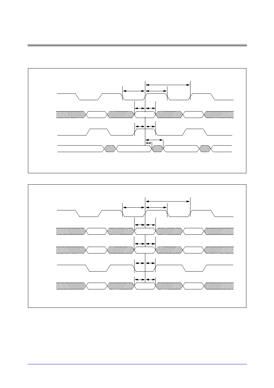
STDL130
5-160
Samsung ASIC
SPSRAMBW_LPL
Low-Power Single-Port Synchronous Static RAM with Bit-Write
Timing Diagram
Read Cycle
Write Cycle
t
as
A [ ]
t
ah
(CSN = low, OEN = low, BWEN, DI = don't care)
t
acc
WEN
t
ws
t
wh
t
da
DOUT [ ]
t
cyc
CK
t
ckl
t
ckh
A0
A2
Valid
M[A0]
M[A1]
M[A2]
A1
t
as
A [ ]
t
ah
(CSN = low, OEN = don't care)
WEN
t
ws
t
wh
DI [ ]
t
cyc
CK
t
ckl
t
ckh
A0
A2
t
ds
t
dh
D0
D2
t
bws
BWEN [ ]
t
bwh
BW0
BW2
BW1
A1
D1
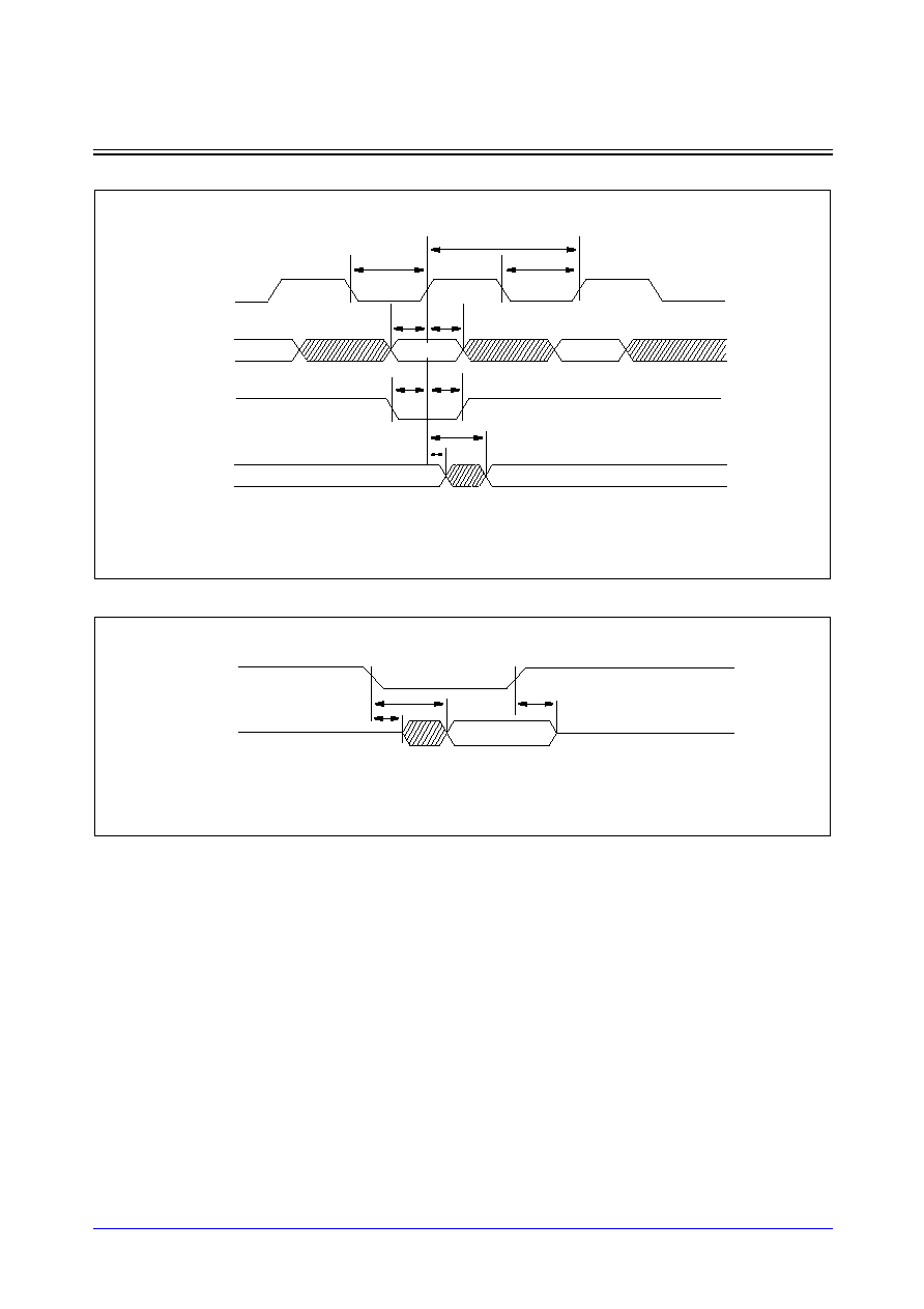
Samsung ASIC
5-161
STDL130
SPSRAMBW_LPL
Low-Power Single-Port Synchronous Static RAM with Bit-Write
Read Cycle with CSN Controlled
OEN Controlled Output Enable
NOTE: "don't care" means the condition that these pins are in normal operation mode.
t
as
A [ ]
t
ah
(OEN = low, WEN = high, BWEN, DI = don't care)
CSN
t
cs
t
ch
DOUT [ ]
t
cyc
CK
t
ckl
t
ckh
A0
A2
A1
t
da
t
acc
M(A1)
M(A0)
(CK, A, WEN, BWEN, DI, CSN = don't care)
t
od
t
dz
Hi-Z
Valid
OEN
DOUT [ ]
Hi-Z
t
zd

STDL130
5-162
Samsung ASIC
DPSRAM_LPL
Low-Power Dual-Port Synchronous Static RAM
Logic Symbol
Function Description
DPSRAM_LPL is a dual-port synchronous static RAM which is provided as a compiler. DPSRAM_LPL is
intended for use in low-power applications. Each port is fully independent. On the rising edge of CK1 (CK2),
the write cycle is initiated when WEN1 (WEN2) is low and CSN1 (CSN2) is low. The data on DI1[] (DI2[]) is
written into the memory location specified on A1[](A2[]). During the write cycle, DOUT1[] (DOUT2[]) remains
stable. On the rising edge of CK1 (CK2), the read cycle is initiated when WEN1 (WEN2) is high and
CSN1(CSN2) is low. The data at DOUT1[] (DOUT2[]) become valid after a delay. While in standby mode that
CSN1(CSN2) is high, A1[] (A2[]) and DI1[] (DI2[]) are disabled, data stored in the memory is retained and
DOUT1[] (DOUT2[]) remains stable. When OEN1 (OEN2) is high, DOUT1[] (DOUT2[]) is placed in a
high-impedance state.
DPSRAM_LPL Function Table
CK1
CK2
CSN1
CSN2
WEN1
WEN2
OEN1
OEN2
A1
A2
DI1
DI2
DOUT1
DOUT2
Comment
X
X
X
H
X
X
Z
Unconditional tri-state output
X
H
X
L
X
X
DOUT(t-1)
De-selected (standby mode)
L
L
L
Valid
Valid
DOUT(t-1)
Write cycle
L
H
L
Valid
X
MEM(A)
Read cycle
Features
∑
Suitable for low-power application
∑
Separated data I/O
∑
Synchronous operation
∑
Duty-free clock cycle
∑
Asynchronous tri-state ouput control
∑
Latched inputs and outputs
∑
Automatic power-down
∑
Zero standby current
∑
Zero hold time
∑
Low noise output optimizatioin
∑
Flexible aspect ratio
∑
Up to 256Kbits capacity
∑
Up to 16K number of words
∑
Up to 128 number of bit per word
NOTES:
1. Words (w) is the number of words..
2. Bpw (b) is the number of bits per word.
3. Ymux (y) is one of the column mux types.
4. m =
log
2
w
CK1
CK2
CSN1
CSN2
WEN1
dpsram_lpl_<w>x<b>m<y>
DOUT1 [b-1:0]
WEN2
OEN1
OEN2
A1 [m-1:0]
A2 [m-1:0]
DI1 [b-1:0]
DI2 [b-1:0]
DOUT2 [b-1:0]
Samsung ASIC
5-163
STDL130
DPSRAM_LPL
Low-Power Dual-Port Synchronous Static RAM
Parameter Description
DPSRAM_LPL is the compiler that automatically generates symbol, netlist, timing model, power model and
layout according to the following parameters; Number of words(w), Number of bit per word(b) and Column
mux(y).
Pin Descriptions
Pin Capacitance
(Unit = SL)
NOTE: Each pin's capacitance is exactly same regardless of available mux types.
Parameters
Ymux(y) = 2
Ymux(y) = 4
Ymux(y) = 8
Ymux(y) = 16
Words (w)
Min
32
64
128
256
Max
2048
4096
8192
16384
Step
16
32
64
128
Bpw (b)
Min
1
1
1
1
Max
128
64
32
16
Step
1
1
1
1
Name
Type
Description
CK1
CK2
Clock
Clock input. CSN, WEN, A[] and DI[] are latched into the RAM on the rising
edge of CK. If CSN and WEN are low on the rising edge of CK, the RAM is in
write mode. If WEN is high on the rising edge of CK, the RAM is in read
mode. Upon the falling edge of CK, the RAM is in a precharge state.
CSN1
CSN2
Chip
Enable
Chip enable input. The chip enable is active-low and is latched into the RAM
on the rising edge of CK. When CSN is low, the RAM is enabled for reading
or writing, depending on the state of WEN. When CSN is high, the RAM goes
to the standby mode and is disabled for reading or writing. DOUT remains
previous data output.
WEN1
WEN2
Read/Write
Enable
Read or write enable input. The read/write enable is latched into the RAM on
the rising edge of CK. When WEN is low, data are written to the addressed
location and DOUT remains stable. When WEN is high, data from the
addressed word are present at DOUT.
OEN1
OEN2
Data
Output
Enable
Data output enable input. The data output enable is asynchronously operated
regardless of the state of other inputs. When OEN is high, DOUT is disabled
and goes to high-impedance state.
A1 [ ]
A2 [ ]
Address
Address input bus. The address is latched into the RAM on the rising edge of
CK.
DI1 [ ]
DI2 [ ]
Data Input
Data input bus. Data are latched on the rising edge of CK. Data input is
written into the addressed location in write mode.
DOUT1 [ ]
DOUT2 [ ]
Data
Output
Data output bus. Data output is valid after the rising edge of CK while the
RAM is in read mode. Data output remains previous data output while the
RAM is in write mode.
CK
CSN
WEN
OEN
A
DI
DOUT
15.15
3.89
3.83
5.21
3.83
3.83
6.40
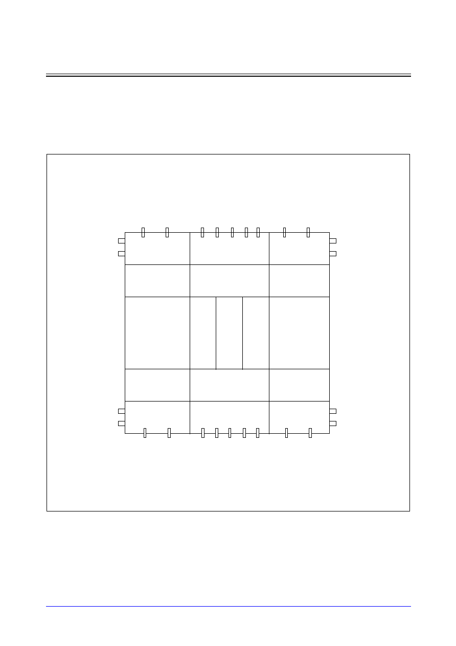
STDL130
5-164
Samsung ASIC
DPSRAM_LPL
Low-Power Dual-Port Synchronous Static RAM
Block Diagram
DPSRAM_LPL supports only 1-bank architecture. The power ports are located on the top-edge and the
bottom edge of both right- and left-sides of the memory. However, DPSRAM_LPL has two symmetrical ports
located on opposite edges of memory. Port1 is located on the bottom of the memory while Port2 is located
on the top of the memory.
I/O Driver
Address &
Clock Buffers
I/O Driver
Y-Dec &
Sense Amp.
Control Block
Y-Dec &
Sense Amp.
RAM Core
W
ord-line Decoder
X-Dec
W
ord-line Decoder
RAM Core
Y-Dec &
Sense Amp.
Control Block
Y-Dec &
Sense Amp.
I/O Driver
Address &
Clock Buffers
I/O Driver
VSS
VDD
VDD
VSS
VSS
VDD
VDD
VSS
DOUT1[b-1:b/2]
DI1[b-1:b/2]
A1[m-1:0]
WEN1
OEN1
CSN1
CK1
DOUT1[b/2-1:0]
DI1[b/2-1:0]
DOUT2[b-1:b/2]
DI2[b-1:b/2]
A2[m-1:0]
WEN2
OEN2
CSN2
CK2
DOUT2[b/2-1:0]
DI2[b/2-1:0]

Samsung ASIC
5-165
STDL130
DPSRAM_LPL
Low-Power Dual-Port Synchronous Static RAM
Application Notes
1.
Permitting over-the-cell routing. In chip-level layout, over-the-cell routing in DPSRAM_LPL is permitted
for only Metal-5 and Metal-6 layers.
2.
Incoming power bus should be adjusted to guarantee NOT more than 10% voltage drop at typical-case
current levels.
3.
Power stripe should be tapped from both sides of DPSRAM_LPL.
4.
Contention mode in same address access.
In DPSRAM_LPL, simultaneous operation by both ports on the same memory address, as write/write,
write/read or read/write operation, causes a contention problem. Simultaneous operation is defined as a
state in which both ports are enabled, both address buses are equal at the rising edge of CK.
DPSRAM_LPL has no scheme preventing the contention. Due to simultaneous operation, silicon will
behave unpredictably. A write operation cannot end and data appearing at outputs may not be valid.
Please refer to the timing diagrams if you want to avoid the contention mode between both ports. In
write/write operation, the data stored at the current address will be unpredictable. In write/read or
read/write operation, the read port is invalid while the write port is still valid. If you want to avoid the
contention mode, you have to give the value greater than tcc (clock-to-clock setup time). However,
simultaneous read/read is allowable without any restrictions.
5.
Power reduction during standby mode.
The standby power is measured on the condition that only CSN is disable mode and other signals are in
operation mode except that OEN is tied to low. If any of signals are activated while in standby mode, the
power will be consumed because the input switching activities are occurred by the signal transition.
Therefore, to reduce unnecessary power consumption, you should keep stable for all signals while in
standby mode.

STDL130
5-166
Samsung ASIC
DPSRAM_LPL
Low-Power Dual-Port Synchronous Static RAM
Characteristics
Definition for AC Timing (ns)
Symbol
Description
Symbol
Description
t
cyc
Clock cycle time
t
ckl
Clock pulse width low
t
ckh
Clock pulse width high
t
cc
Clock to Clock Setup time
t
as
Address setup time
t
ah
Address hold time
t
cs
CSN setup time
t
ch
CSN hold time
t
ds
Data-In setup time
t
dh
Data-In hold time
t
ws
WEN setup time
t
wh
WEN hold time
t
acc
Data access time
t
da
De-access time
t
dz
DOUT drive to high-Z time
t
zd
DOUT high-Z to drive time
t
od
OEN to valid output time
Definition for Power Consumption (
µ
W/MHz)
Power_read
The dynamic average power consumption while in a read cycle
Power_write
The dynamic average power consumption while in a write cycle
Power_standby
The standby power consumption while CSN is high, OEN is low and other signals are in
normal operation
Definition for Area (
µ
m)
Width
The physical width in X-direction
Height
The physical height in Y-direction

Samsung ASIC
5-167
STDL130
DPSRAM_LPL
Low-Power Dual-Port Synchronous Static RAM
Reference Table
* For Ymux=2
(Typical process, 1.8V, 25
∞
C, Output load = 10SL, Input slope = 0.2 ns, SA=0.5)
NOTES:
1.
In power consumption of DPSRAM_LPL, only one port is measured and the other port is isolated.
2.
Standby power is measured on the condition that other signals are in normal operation while CSN is in disable
mode and OEN is tied to low.
Parameters
words
32
64
128
256
512
1024
1536
2048
bpw
16
32
48
64
80
96
112
128
Timing (ns)
t
cyc
2.83
2.85
2.88
2.90
2.92
3.19
3.47
3.73
t
ckl
0.92
0.92
0.92
0.92
0.92
0.92
0.92
0.92
t
ckh
0.91
0.91
0.91
0.91
0.91
0.91
0.91
0.91
t
cc
1.59
1.61
1.63
1.65
1.67
1.96
2.27
2.59
t
as
0.26
0.26
0.26
0.26
0.26
0.26
0.26
0.26
t
ah
0.01
0.01
0.01
0.01
0.01
0.01
0.01
0.01
t
cs
0.27
0.27
0.27
0.27
0.27
0.28
0.28
0.28
t
ch
0.01
0.01
0.01
0.01
0.01
0.01
0.01
0.01
t
ds
0.23
0.21
0.20
0.19
0.18
0.17
0.15
0.14
t
dh
0.01
0.01
0.01
0.01
0.01
0.01
0.01
0.01
t
ws
0.45
0.45
0.45
0.45
0.45
0.45
0.45
0.45
t
wh
0.01
0.01
0.01
0.01
0.01
0.01
0.01
0.01
t
acc
2.50
2.52
2.55
2.57
2.59
2.86
3.14
3.40
t
da
2.41
2.42
2.44
2.45
2.47
2.73
3.00
3.26
t
dz
0.35
0.37
0.39
0.41
0.43
0.45
0.46
0.48
t
zd
0.39
0.41
0.43
0.45
0.47
0.49
0.51
0.53
t
od
0.44
0.46
0.48
0.50
0.52
0.54
0.56
0.58
Power (
µ
W/MHz)
Power_read
56.84
85.59
115.63
148.62
188.29
233.49
275.58
319.16
Power_write
55.03
81.92
111.96
149.42
204.00
280.26
368.19
467.16
Power_standby
3.32
5.53
7.75
10.00
12.31
14.76
17.00
19.28
Area (
µ
m)
Width
377.24
550.04
722.84
895.64
1068.44
1241.24
1414.04
1586.84
Height
221.56
252.01
312.90
434.70
678.28
1174.60
1670.92
2167.24

STDL130
5-168
Samsung ASIC
DPSRAM_LPL
Low-Power Dual-Port Synchronous Static RAM
Reference Table
* For Ymux=4
(Typical process, 1.8V, 25
∞
C, Output load = 10SL, Input slope = 0.2 ns, SA=0.5)
NOTES:
1.
In power consumption of DPSRAM_LPL, only one port is measured and the other port is isolated.
2.
Standby power is measured on the condition that other signals are in normal operation while CSN is in disable
mode and OEN is tied to low.
Parameters
words
64
128
256
512
1024
2048
3072
4096
bpw
8
16
24
32
40
48
56
64
Timing (ns)
t
cyc
2.82
2.84
2.85
2.87
2.89
3.15
3.41
3.67
t
ckl
0.92
0.92
0.92
0.92
0.92
0.92
0.92
0.92
t
ckh
0.91
0.91
0.91
0.91
0.91
0.91
0.91
0.91
t
cc
1.59
1.61
1.63
1.65
1.67
1.96
2.27
2.59
t
as
0.26
0.26
0.26
0.26
0.26
0.26
0.26
0.26
t
ah
0.01
0.01
0.01
0.01
0.01
0.01
0.01
0.01
t
cs
0.27
0.27
0.27
0.27
0.27
0.28
0.28
0.28
t
ch
0.01
0.01
0.01
0.01
0.01
0.01
0.01
0.01
t
ds
0.23
0.22
0.21
0.20
0.19
0.18
0.17
0.16
t
dh
0.01
0.01
0.02
0.01
0.01
0.01
0.01
0.01
t
ws
0.45
0.45
0.45
0.45
0.45
0.45
0.45
0.45
t
wh
0.01
0.01
0.01
0.01
0.01
0.01
0.01
0.01
t
acc
2.49
2.51
2.52
2.54
2.56
2.82
3.08
3.34
t
da
2.41
2.41
2.42
2.44
2.45
2.71
2.97
3.22
t
dz
0.35
0.36
0.37
0.39
0.40
0.42
0.43
0.44
t
zd
0.39
0.40
0.41
0.43
0.44
0.46
0.47
0.49
t
od
0.43
0.45
0.46
0.48
0.49
0.51
0.52
0.54
Power (
µ
W/MHz)
Power_read
45.03
62.21
80.99
103.46
134.32
166.60
194.72
223.40
Power_write
44.68
60.56
78.77
102.48
138.83
187.60
244.37
307.15
Power_standby
2.24
3.35
4.47
5.62
6.83
8.16
9.28
10.42
Area (
µ
m)
Width
377.24
550.04
722.84
895.64
1068.44
1241.24
1414.04
1586.84
Height
221.56
252.01
312.90
434.70
678.28
1174.60
1670.92
2167.24
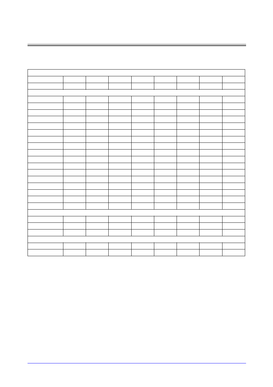
Samsung ASIC
5-169
STDL130
DPSRAM_LPL
Low-Power Dual-Port Synchronous Static RAM
Reference Table
* For Ymux=8
(Typical process, 1.8V, 25
∞
C, Output load = 10SL, Input slope = 0.2 ns, SA=0.5)
NOTES:
1.
In power consumption of DPSRAM_LPL, only one port is measured and the other port is isolated.
2.
Standby power is measured on the condition that other signals are in normal operation while CSN is in disable
mode and OEN is tied to low.
Parameters
words
128
256
512
1024
2048
4096
6144
8192
bpw
4
8
12
16
20
24
28
32
Timing (ns)
t
cyc
2.84
2.85
2.87
2.88
2.90
3.16
3.43
3.69
t
ckl
0.92
0.92
0.92
0.92
0.92
0.91
0.91
0.91
t
ckh
0.91
0.91
0.91
0.91
0.91
0.91
0.91
0.91
t
cc
1.59
1.61
1.63
1.65
1.68
1.96
2.27
2.59
t
as
0.26
0.26
0.26
0.26
0.26
0.26
0.26
0.26
t
ah
0.01
0.01
0.01
0.01
0.01
0.01
0.01
0.01
t
cs
0.27
0.27
0.27
0.27
0.27
0.27
0.27
0.27
t
ch
0.01
0.01
0.01
0.01
0.01
0.01
0.01
0.01
t
ds
0.23
0.22
0.21
0.20
0.19
0.18
0.17
0.16
t
dh
0.01
0.01
0.01
0.01
0.01
0.01
0.01
0.01
t
ws
0.45
0.45
0.45
0.45
0.45
0.45
0.45
0.45
t
wh
0.01
0.01
0.01
0.01
0.01
0.01
0.01
0.01
t
acc
2.51
2.52
2.54
2.55
2.57
2.83
3.10
3.36
t
da
2.42
2.43
2.44
2.45
2.46
2.72
2.98
3.24
t
dz
0.35
0.36
0.37
0.39
0.40
0.42
0.43
0.44
t
zd
0.39
0.40
0.42
0.43
0.45
0.46
0.48
0.49
t
od
0.43
0.45
0.46
0.48
0.49
0.51
0.52
0.54
Power (
µ
W/MHz)
Power_read
41.24
54.85
70.08
89.08
116.64
144.73
168.53
192.69
Power_write
44.81
57.98
72.87
91.83
120.05
154.10
194.31
237.22
Power_standby
1.72
2.28
2.86
3.46
4.12
4.90
5.44
6.01
Area (
µ
m)
Width
377.24
550.04
722.84
895.64
1068.44
1241.24
1414.04
1586.84
Height
221.56
252.01
312.90
434.70
678.28
1174.60
1670.92
2167.24
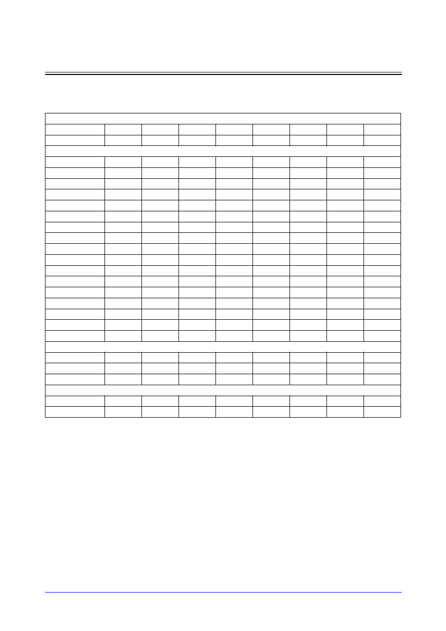
STDL130
5-170
Samsung ASIC
DPSRAM_LPL
Low-Power Dual-Port Synchronous Static RAM
Reference Table
* For Ymux=16
(Typical process, 1.8V, 25
∞
C, Output load = 10SL, Input slope = 0.2 ns, SA=0.5)
NOTES:
1.
In power consumption of DPSRAM_LPL, only one port is measured and the other port is isolated.
2.
Standby power is measured on the condition that other signals are in normal operation while CSN is in disable
mode and OEN is tied to low.
Parameters
words
256
512
1024
2048
4096
8192
12288
16384
bpw
2
4
6
8
10
12
14
16
Timing (ns)
t
cyc
2.87
2.88
2.89
2.91
2.93
3.19
3.45
3.72
t
ckl
0.92
0.92
0.92
0.92
0.92
0.91
0.91
0.91
t
ckh
0.91
0.91
0.91
0.91
0.91
0.91
0.91
0.91
t
cc
1.59
1.61
1.63
1.65
1.68
1.96
2.27
2.59
t
as
0.26
0.26
0.26
0.26
0.26
0.26
0.26
0.26
t
ah
0.01
0.01
0.01
0.01
0.01
0.01
0.01
0.01
t
cs
0.27
0.27
0.27
0.27
0.27
0.27
0.27
0.27
t
ch
0.01
0.01
0.01
0.01
0.01
0.01
0.01
0.01
t
ds
0.22
0.21
0.19
0.18
0.16
0.15
0.14
0.12
t
dh
0.01
0.01
0.01
0.02
0.02
0.02
0.02
0.03
t
ws
0.45
0.45
0.45
0.45
0.45
0.45
0.45
0.45
t
wh
0.01
0.01
0.01
0.01
0.01
0.01
0.01
0.01
t
acc
2.54
2.55
2.56
2.58
2.60
2.86
3.12
3.39
t
da
2.45
2.46
2.47
2.48
2.49
2.75
3.01
3.26
t
dz
0.35
0.37
0.39
0.41
0.43
0.44
0.46
0.48
t
zd
0.39
0.41
0.43
0.45
0.47
0.49
0.51
0.53
t
od
0.44
0.46
0.48
0.50
0.52
0.54
0.56
0.58
Power (
µ
W/MHz)
Power_read
38.78
50.25
63.35
80.27
105.82
131.50
152.77
174.25
Power_write
43.30
54.81
67.76
84.02
107.82
134.42
165.85
198.60
Power_standby
1.44
1.73
2.02
2.35
2.75
3.24
3.51
3.80
Area (
µ
m)
Width
377.24
550.04
722.84
895.64
1068.44
1241.24
1414.04
1586.84
Height
221.56
252.01
312.90
434.70
678.28
1174.60
1670.92
2167.24

Samsung ASIC
5-171
STDL130
DPSRAM_LPL
Low-Power Dual-Port Synchronous Static RAM
Timing Diagrams
Read Cycle
Write Cycle
t
as
A [ ]
t
ah
(CSN = low, OEN = low, DI[ ] = don't care)
t
acc
WEN
t
ws
t
wh
t
da
DOUT [ ]
t
cyc
CK
t
ckl
t
ckh
A0
A2
Valid
M[A0]
M[A1]
M[A2]
A1
t
as
A [ ]
t
ah
(CSN= low, OEN = don't care)
WEN
t
ws
t
wh
DI [ ]
t
cyc
CK
t
ckl
t
ckh
A0
A2
A1
t
ds
t
dh
D0
D2
D1

STDL130
5-172
Samsung ASIC
DPSRAM_LPL
Low-Power Dual-Port Synchronous Static RAM
Read Cycle with CSN Controlled
OEN Controlled Output Enable
Contention Mode
NOTE: "don't care" means the condition that these pins are in normal operation mode.
t
as
A [ ]
t
ah
(OEN = low, WEN = high, DI[ ]= don't care)
CSN
t
cs
t
ch
DOUT [ ]
t
cyc
CK
t
ckl
t
ckh
A0
A2
A1
t
da
t
acc
M[A1]
M[A0]
(CSN = low, CK, A[ ], WEN, DI[ ] = don't care)
t
od
t
dz
Hi-Z
Valid
OEN
DOUT [ ]
Hi-Z
t
zd
CK1
tcc
CK2
(A1[ ] = A2[ ])
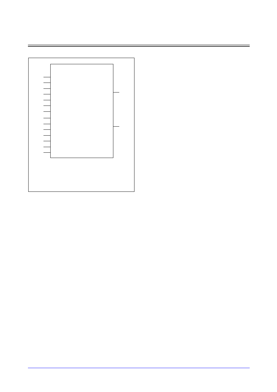
Samsung ASIC
5-173
STDL130
DPSRAMBW_LPL
Low-Power Dual-Port Synchronous Static RAM with Bit-Write
Logic Symbol
Function Description
DPSRAMBW_LPL is a dual-port synchronous static RAM with bit-write capability which is provided as a
compiler. DPSRAMBW_LPL is intended for use in Low-Power applications. Each port is fully independent.
Basically, its functionality is exactly same as DPSRAM_HDL except a bit-write operation which is controlled
by BWEN1[](BWEN2[]), named bit-write enable signal bus. Each bit of BWEN1[](BWEN2[]) enables or
disable the write operation of its corresponding bit in DI1[](DI2[]). On the rising edge of CK1(CK2), the write
cycle is initiated when WEN1(WEN2) is low and CSN1(CSN2) is low. The data bits in DI1[](DI2[]), which
their corresponding bit(s) in BWEN1[](BWEN2[]) are low, are written into the memory location specified on
A1[](A2[]). When all bits of BWEN1[](BWEN2[]) are high, any data in DI1[](DI2[]) are not written into the
memory location specified on A1[](A2[]). When all bits of BWEN1[](BWEM2[]) are low, the data in
DI1[](DI2[]) are written into the memory location specified on A1[](A2[]), which is exactly same as the write
operation in DPSRAM_LPL. During the write cycle, DOUT1[](DOUT2[]) remains stable. On the rising edge
of CK1(CK2), the read cycle is initiated when WEN1(WEN2) is high and CSN1(CSN2) is low. The data at
DOUT1[](DOUT2[]) become valid after a delay. While in standby mode that CSN1(CSN2) is high, A1[](A2[])
and DI1[](DI2[]) are disabled, data stored in the memory is retained and DOUT1[](DOUT2[]) remains stable.
When OEN1(OEN2) is high, DOUT1[](DOUT2[]) is placed in a high-impedance state.
Features
∑
Suitable for low-power application
∑
Separated data I/O
∑
Synchronous operation
∑
Duty-free clock cycle
∑
Asynchronous tri-state ouput control
∑
Latched inputs and outputs
∑
Automatic power-down
∑
Zero standby current
∑
Zero hold time
∑
Low noise output optimizatioin
∑
Flexible aspect ratio
∑
Up to 256Kbits capacity
∑
Up to 16K number of words
∑
Up to 128 number of bit per word
NOTES:
1. Words (w) is the number of words..
2. Bpw (b) is the number of bits per word.
3. Ymux (y) is one of the column mux types.
4. m =
log
2
w
CK1
CK2
CSN1
CSN2
WEN1
dpsrambw_lpl_<w>x<b>m<y>
DOUT1 [b-1:0]
WEN2
OEN1
OEN2
A1 [m-1:0]
A2 [m-1:0]
DI1 [b-1:0]
DI2 [b-1:0]
DOUT2 [b-1:0]
BWEN1 [b-1:0]
BWEN2 [b-1:0]
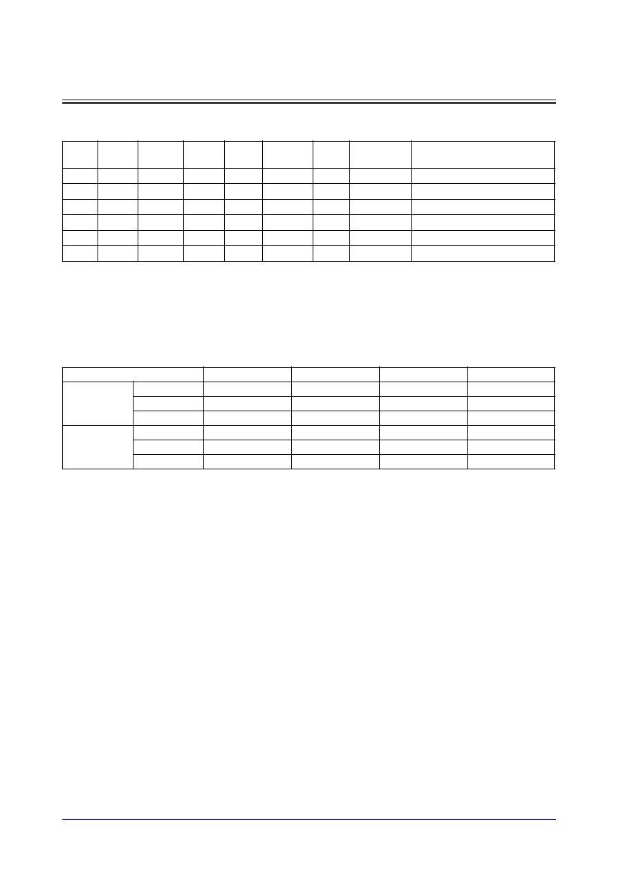
STDL130
5-174
Samsung ASIC
DPSRAMBW_LPL
Low-Power Dual-Port Synchronous Static RAM with Bit-Write
DPSRAMBW_LPL Function Table
Parameter Description
DPSRAMBW_LPL is the compiler that automatically generates symbol, netlist, timing model, power model
and layout according to the following parameters; Number of words(w), Number of bit per word(b) and
Column mux(y).
CK1
CK2
CSN1
CSN2
WEN1
WEN2
OEN1
OEN2
A1
A2
BWEN1
BWEN2
DI1
DI2
DOUT1
DOUT2
Comment
X
X
X
H
X
X
X
Z
Unconditional tri-state output
X
H
X
L
X
X
X
DOUT(t-1)
De-selected (standby mode)
L
L
L
Valid
all L
Valid
DOUT(t-1)
Word-write cycle
L
L
L
Valid
L
Valid
DOUT(t-1)
Bit-write cycle
L
L
L
Valid
all H
Valid
DOUT(t-1)
No operation
L
H
L
Valid
X
X
MEM(A)
Read cycle
Parameters
Ymux(y) = 2
Ymux(y) = 4
Ymux(y) = 8
Ymux(y) = 16
Words (w)
Min
32
64
128
256
Max
2048
4096
8192
16384
Step
16
32
64
128
Bpw (b)
Min
1
1
1
1
Max
128
64
32
16
Step
1
1
1
1
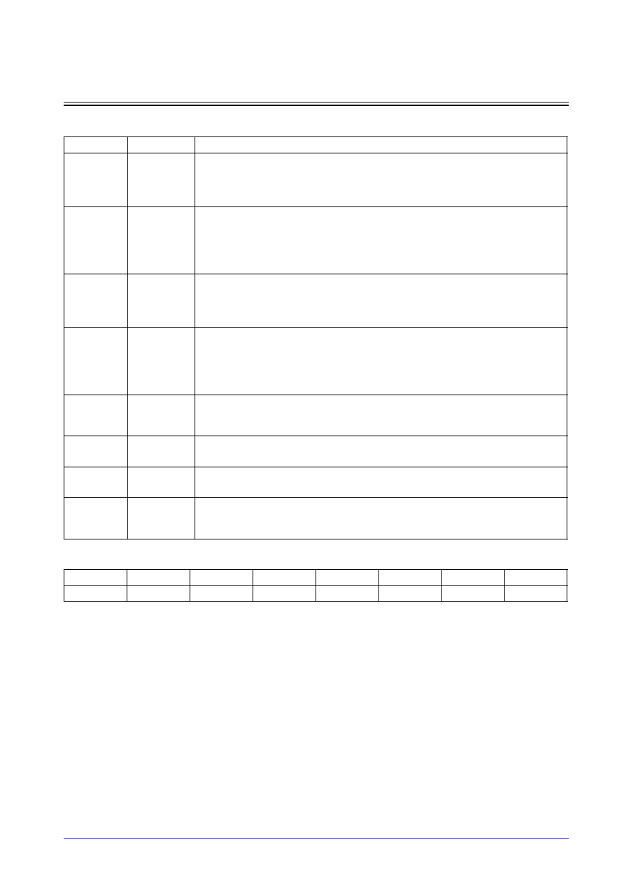
Samsung ASIC
5-175
STDL130
DPSRAMBW_LPL
Low-Power Dual-Port Synchronous Static RAM with Bit-Write
Pin Descriptions
Pin Capacitance
(Unit = SL)
NOTE: Each pin's capacitance is exactly same regardless of available mux types.
Name
Type
Description
CK1
CK2
Clock
Clock input. CSN, WEN, A[] and DI[] are latched into the RAM on the rising
edge of CK. If CSN and WEN are low on the rising edge of CK, the RAM is in
write mode. If WEN is high on the rising edge of CK, the RAM is in read
mode. Upon the falling edge of CK, the RAM is in a precharge state.
CSN1
CSN2
Chip
Enable
Chip Enable input. The chip enable is active-low and is latched into the RAM
on the rising edge of CK. When CSN is low, the RAM is enabled for reading
or writing, depending on the state of WEN. When CSN is high, the RAM goes
to the standby mode and is disabled for reading or writing. DOUT remains
previous data output.
WEN1
WEN2
Read/Write
Enable
Read or write enable input. The read/write enable is latched into the RAM on
the rising edge of CK. When WEN is low, data are written to the addressed
location and DOUT remains stable. When WEN is high, data from the
addressed word are present at DOUT.
BWEN1 [ ]
BWEN2 [ ]
Bit-Write
Enable
Bit-write enable input bus. The bit-write enable is latched into the RAM on the
rising edge of CK. Each bit of BWEN[] enables/disables the write operation of
corresponding data bit. BWEN[i] corresponds to DI[i] in bit-write. If WEN and
BWEN[0] are low and BWEN[1] is high, DI[0] is written into the memory
location specified on A[], but DI[1] is not written.
OEN1
OEN2
Data
Output
Enable
Data output enable input. The data output enable is asynchronously operated
regardless of the state of other inputs. When OEN is high, DOUT is disabled
and goes to high-impedance state.
A1 [ ]
A2 [ ]
Address
Address input bus. The address is latched into the RAM on the rising edge of
CK.
DI1 [ ]
DI2 [ ]
Data Input
Data input bus. Data are latched on the rising edge of CK. Data input is
written into the addressed location in write mode.
DOUT1 [ ]
DOUT2 [ ]
Data
Output
Data output bus. Data output is valid after the rising edge of CK while the
RAM is in read mode. Data output remains previous data output while the
RAM is in write mode.
CK
CSN
WEN
BWEN
OEN
A
DI
DOUT
15.15
3.89
3.83
3.93
5.21
3.83
3.83
6.40
STDL130
5-176
Samsung ASIC
DPSRAMBW_LPL
Low-Power Dual-Port Synchronous Static RAM with Bit-Write
Block Diagram
DPSRAMBW_LPL supports only 1-bank architecture. The power ports are located on the top-edge and the
bottom edge of both right- and left-sides of the memory. However, DPSRAMBW_LPL has two symmetrical
ports located on opposite edges of memory. Port1 is located on the bottom of the memory while Port2 is
located on the top of the memory.
I/O Driver
Address &
Clock Buffers
I/O Driver
Y-Dec &
Sense Amp.
Control Block
Y-Dec &
Sense Amp.
RAM Core
W
ord-line Decoder
X-Dec
W
ord-line Decoder
RAM Core
Y-Dec &
Sense Amp.
Control Block
Y-Dec &
Sense Amp.
I/O Driver
Address &
Clock Buffers
I/O Driver
VSS
VDD
VDD
VSS
VSS
VDD
VDD
VSS
DOUT1[b-1:b/2]
DI1[b-1:b/2]
A1[m-1:0]
WEN1
OEN1
CSN1
CK1
DOUT1[b/2-1:0]
DI1[b/2-1:0]
DOUT2[b-1:b/2]
DI2[b-1:b/2]
A2[m-1:0]
WEN2
OEN2
CSN2
CK2
DOUT2[b/2-1:0]
DI2[b/2-1:0]
BWEN1[b/2-1:0]
BWEN2[b/2-1:0]
BWEN1[b-1:b/2]
BWEN2[b-1:b/2]

Samsung ASIC
5-177
STDL130
DPSRAMBW_LPL
Low-Power Dual-Port Synchronous Static RAM with Bit-Write
Application Notes
1.
Permitting over-the-cell routing.
In chip-level layout, over-the-cell routing in DPSRAMBW_LPL is permitted for only Metal-5 layer and
Metal-6 layers.
2.
Incoming power bus should be adjusted to guarantee NOT more than 10% voltage drop at typical-case
current levels.
3.
Power stripe should be tapped from both sides of DPSRAMBW_LPL.
4.
Contention mode in same address access.
In DPSRAMBW_LPL, simultaneous operation by both ports on the same memory address, as
write/write, write/read or read/write operation, causes a contention problem. Simultaneous operation is
defined as a state in which both ports are enabled, both address buses are equal at the rising edge of
CK. DPSRAMBW_LPL has no scheme preventing the contention. Due to simultaneous operation,
silicon will behave unpredictably. A write operation cannot end and data appearing at outputs may not
be valid. Please refer to the timing diagrams if you want to avoid the contention mode between both
ports. In write/write operation, the data stored at the current address will be unpredictable. In write/read
or read/write operation, the read port is invalid while the write port is still valid. If you want to avoid the
contention mode, you have to give the value greater than tcc (clock-to-clock setup time). However,
simultaneous read/read is allowable without any restrictions.
5.
A byte-write or word-write operation with DPSRAMBW_LPL.
Refer to the function table. In byte-write operation, the number of BWEN[] signal bus should be divided
by a byte (8) and eight BWEN signals should be tied to a connection wire. In this case, DI[] bus is
controlled by a byte-wired BWEN signal instead of each BWEN bit. In word-write operation, the
functionality is exactly same as DPSRAM_LPL. If all of BWEN[] signal is tied to low state, DI[] bus is only
controlled by WEN.
6.
Power reduction during standby mode.
The standby power is measured on the condition that only CSN is disable mode and other signals are in
operation mode except that OEN is tied to low. If any of signals are activated while in standby mode, the
power will be consumed because the input switching activities are occurred by the signal transition.
Therefore, to reduce unnecessary power consumption, you should keep stable for all signals while in
standby mode.
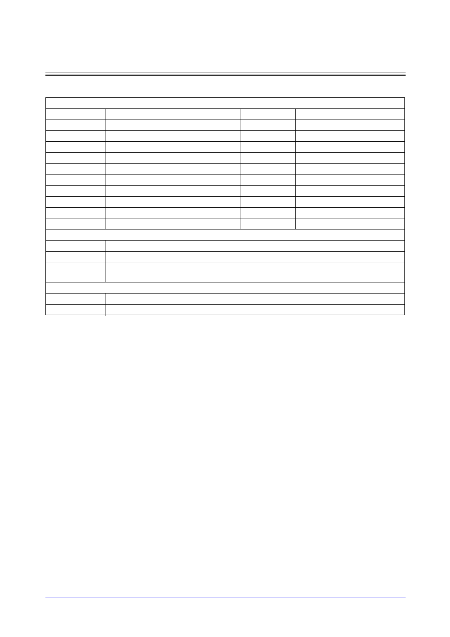
STDL130
5-178
Samsung ASIC
DPSRAMBW_LPL
Low-Power Dual-Port Synchronous Static RAM with Bit-Write
Characteristics
Definition for AC Timing (ns)
Symbol
Description
Symbol
Description
t
cyc
Clock cycle time
t
ckl
Clock pulse width low
t
ckh
Clock pulse width high
t
cc
Clock to Clock Setup time
t
as
Address setup time
t
ah
Address hold time
t
cs
CSN setup time
t
ch
CSN hold time
t
ds
Data-In setup time
t
dh
Data-In hold time
t
ws
WEN setup time
t
wh
WEN hold time
t
bws
BWEN setup time
t
bwh
BWEN hold time
t
acc
Data access time
t
da
De-access time
t
dz
DOUT drive to high-Z time
t
zd
DOUT high-Z to drive time
t
od
OEN to valid output time
Definition for Power Consumption (
µ
W/MHz)
Power_read
The dynamic average power consumption while in a read cycle
Power_write
The dynamic average power consumption while in a write cycle
Power_standby
The standby power consumption while CSN is high, OEN is low and other signals are in
normal operation
Definition for Area (
µ
m)
Width
The physical width in X-direction
Height
The physical height in Y-direction
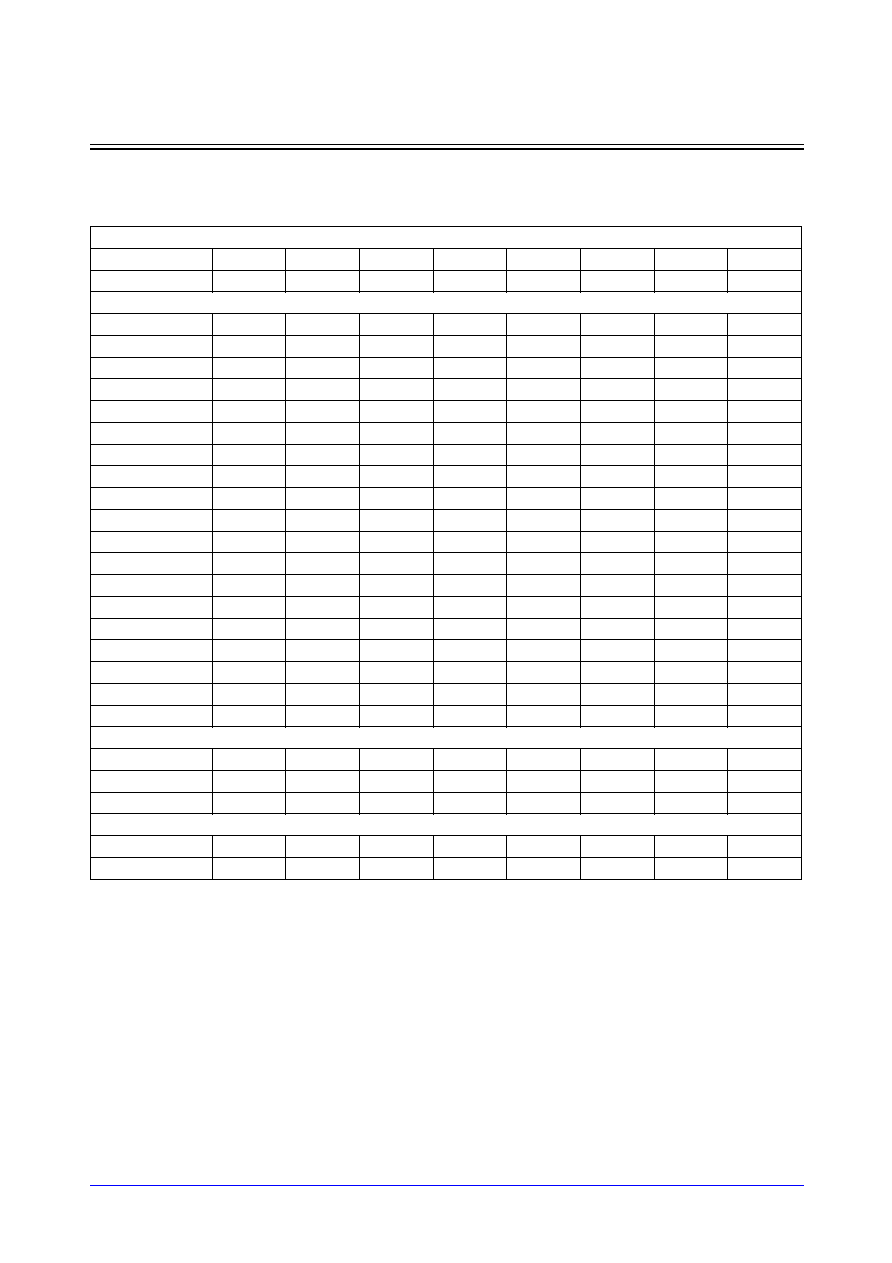
Samsung ASIC
5-179
STDL130
DPSRAMBW_LPL
Low-Power Dual-Port Synchronous Static RAM with Bit-Write
Reference Table
* For Ymux=2
(Typical process, 1.8V, 25
∞
C, Output load = 10SL, Input slope = 0.2 ns, SA=0.5)
NOTES:
1.
In power consumption of DPSRAMBW_LPL, only one port is measured and the other port is isolated.
2.
Standby power is measured on the condition that other signals are in normal operation while CSN is in disable
mode and OEN is tied to low.
Parameters
words
32
64
128
256
512
1024
1536
2048
bpw
16
32
48
64
80
96
112
128
Timing (ns)
t
cyc
2.83
2.85
2.88
2.90
2.92
3.19
3.47
3.73
t
ckl
0.92
0.92
0.92
0.92
0.92
0.92
0.92
0.92
t
ckh
0.91
0.91
0.91
0.91
0.91
0.91
0.91
0.91
t
cc
1.59
1.61
1.63
1.65
1.67
1.96
2.27
2.59
t
as
0.26
0.26
0.26
0.26
0.26
0.26
0.26
0.26
t
ah
0.01
0.01
0.01
0.01
0.01
0.01
0.01
0.01
t
cs
0.27
0.27
0.27
0.27
0.27
0.28
0.28
0.28
t
ch
0.01
0.01
0.01
0.01
0.01
0.01
0.01
0.01
t
ds
0.23
0.21
0.20
0.19
0.18
0.17
0.15
0.14
t
dh
0.01
0.01
0.01
0.01
0.01
0.01
0.01
0.01
t
ws
0.45
0.45
0.45
0.45
0.45
0.45
0.45
0.45
t
wh
0.01
0.01
0.01
0.01
0.01
0.01
0.01
0.01
t
bws
0.23
0.21
0.20
0.19
0.18
0.17
0.15
0.14
t
bwh
0.01
0.01
0.01
0.01
0.01
0.01
0.01
0.01
t
acc
2.50
2.52
2.55
2.57
2.59
2.86
3.14
3.40
t
da
2.41
2.42
2.44
2.45
2.47
2.73
3.00
3.26
t
dz
0.35
0.37
0.39
0.41
0.43
0.45
0.46
0.48
t
zd
0.39
0.41
0.43
0.45
0.47
0.49
0.51
0.53
t
od
0.44
0.46
0.48
0.50
0.52
0.54
0.56
0.58
Power (
µ
W/MHz)
Power_read
56.84
85.59
115.63
148.62
188.29
233.49
275.58
319.16
Power_write
57.24
86.33
118.55
158.20
214.97
293.42
383.54
484.70
Power_standby
5.54
9.93
14.34
18.78
23.28
27.93
32.35
36.83
Area (
µ
m)
Width
377.24
550.04
722.84
895.64
1068.44
1241.24
1414.04
1586.84
Height
221.56
252.01
312.90
434.70
678.28
1174.60
1670.92
2167.24
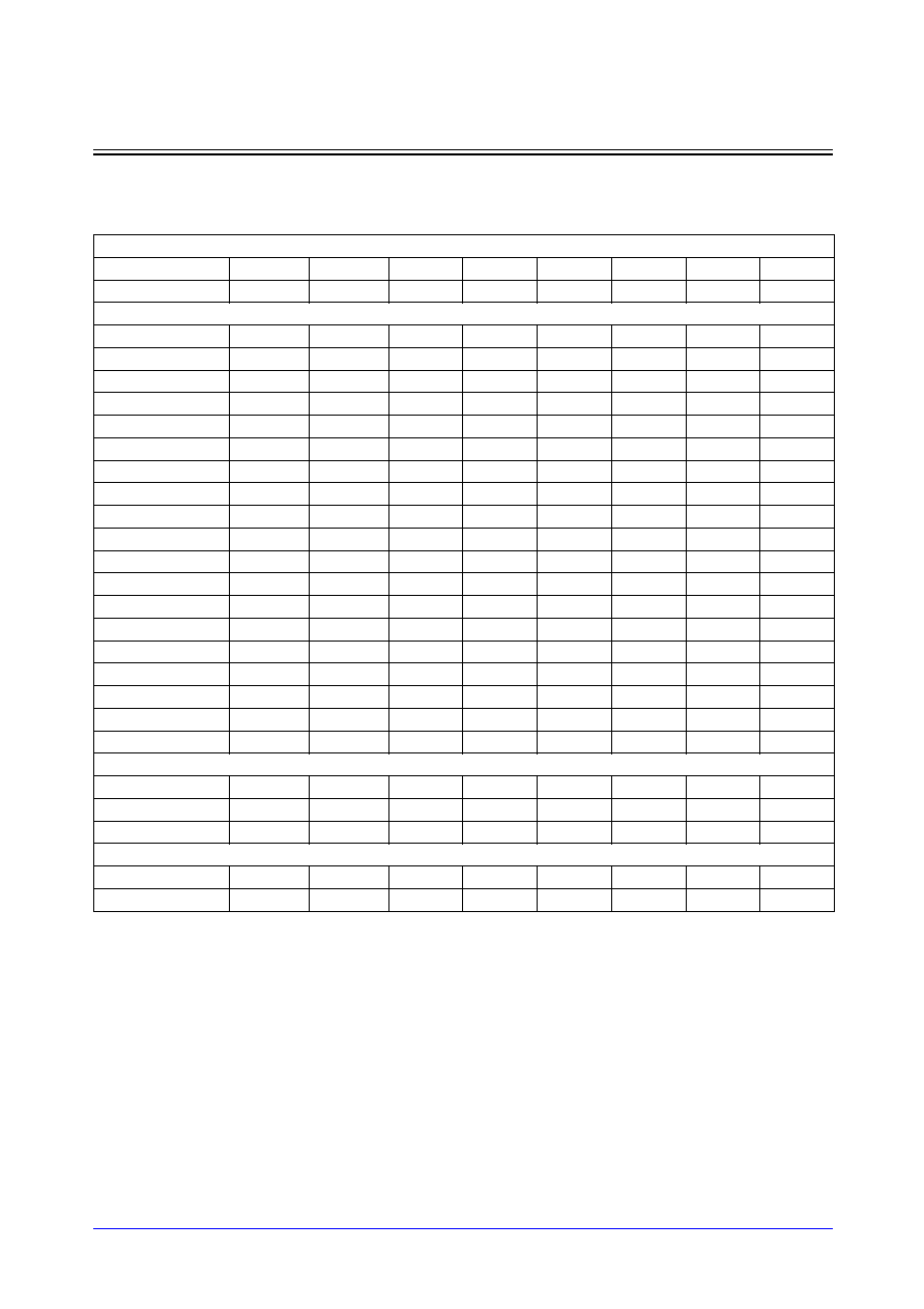
STDL130
5-180
Samsung ASIC
DPSRAMBW_LPL
Low-Power Dual-Port Synchronous Static RAM with Bit-Write
Reference Table
* For Ymux=4
(Typical process, 1.8V, 25
∞
C, Output load = 10SL, Input slope = 0.2 ns, SA=0.5)
NOTES:
1.
In power consumption of DPSRAMBW_LPL, only one port is measured and the other port is isolated.
2.
Standby power is measured on the condition that other signals are in normal operation while CSN is in disable
mode and OEN is tied to low.
Parameters
words
64
128
256
512
1024
2048
3072
4096
bpw
8
16
24
32
40
48
56
64
Timing (ns)
t
cyc
2.82
2.84
2.85
2.87
2.89
3.15
3.41
3.67
t
ckl
0.92
0.92
0.92
0.92
0.92
0.92
0.92
0.92
t
ckh
0.91
0.91
0.91
0.91
0.91
0.91
0.91
0.91
t
cc
1.59
1.61
1.63
1.65
1.67
1.96
2.27
2.59
t
as
0.26
0.26
0.26
0.26
0.26
0.26
0.26
0.26
t
ah
0.01
0.01
0.01
0.01
0.01
0.01
0.01
0.01
t
cs
0.27
0.27
0.27
0.27
0.27
0.28
0.28
0.27
t
ch
0.01
0.01
0.01
0.01
0.01
0.01
0.01
0.01
t
ds
0.23
0.22
0.21
0.20
0.19
0.18
0.17
0.16
t
dh
0.01
0.01
0.01
0.01
0.01
0.01
0.01
0.01
t
ws
0.45
0.45
0.45
0.45
0.45
0.45
0.45
0.45
t
wh
0.01
0.01
0.01
0.01
0.01
0.01
0.01
0.01
t
bws
0.23
0.22
0.21
0.20
0.19
0.18
0.17
0.16
t
bwh
0.01
0.01
0.01
0.01
0.01
0.01
0.01
0.01
t
acc
2.49
2.51
2.52
2.54
2.56
2.82
3.08
3.34
t
da
2.41
2.41
2.42
2.44
2.45
2.71
2.97
3.22
t
dz
0.35
0.36
0.37
0.39
0.40
0.42
0.43
0.44
t
zd
0.39
0.40
0.41
0.43
0.44
0.46
0.47
0.49
t
od
0.43
0.45
0.46
0.48
0.49
0.51
0.52
0.54
Power (
µ
W/MHz)
Power_read
45.03
62.21
80.99
103.46
134.32
166.60
194.72
223.40
Power_write
45.80
62.77
82.07
106.87
144.31
193.68
252.03
315.91
Power_standby
3.36
5.56
7.77
10.01
12.31
14.74
16.95
19.18
Area (
µ
m)
Width
377.24
550.04
722.84
895.64
1068.44
1241.24
1414.04
1586.84
Height
221.56
252.01
312.90
434.70
678.28
1174.60
1670.92
2167.24
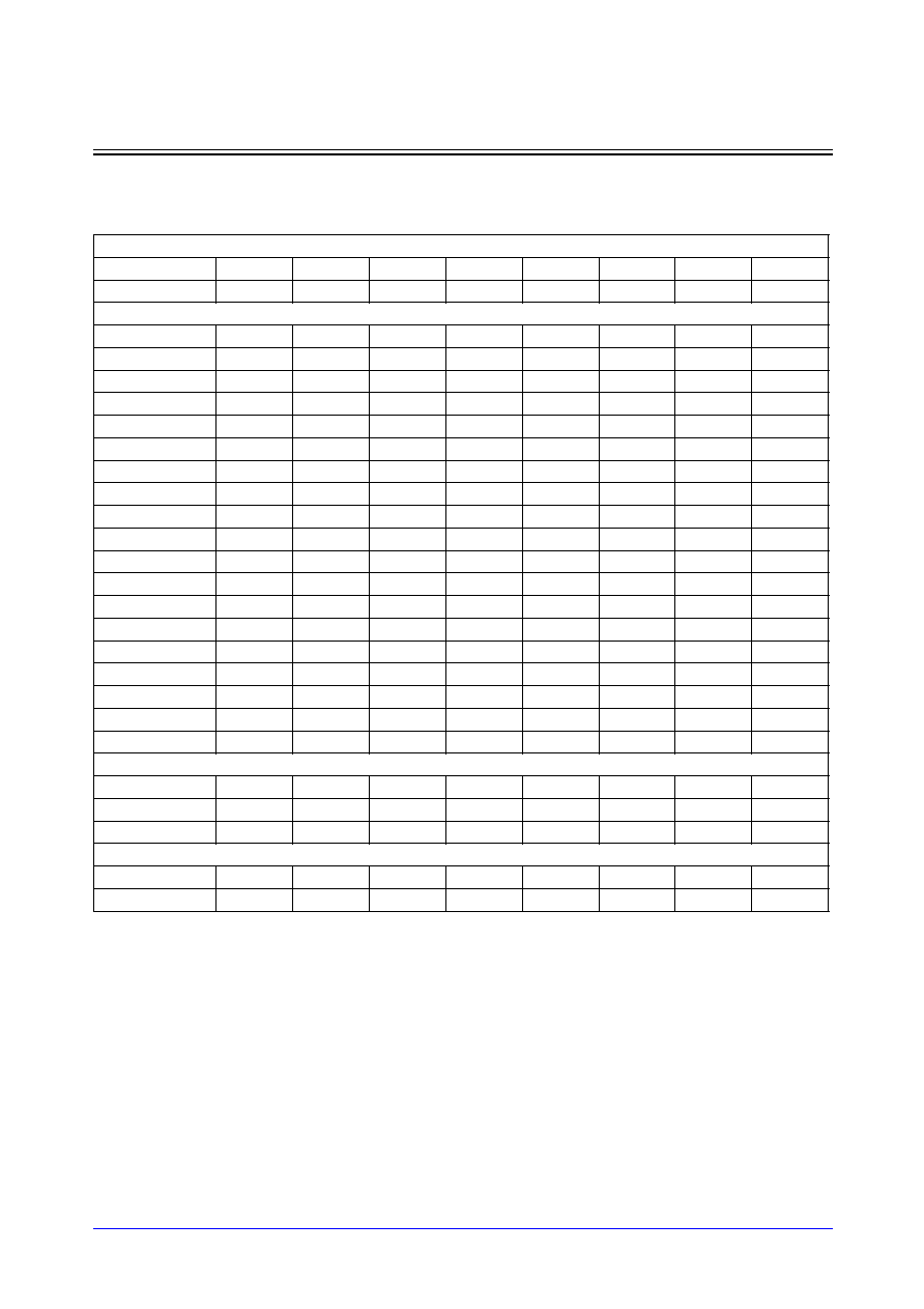
Samsung ASIC
5-181
STDL130
DPSRAMBW_LPL
Low-Power Dual-Port Synchronous Static RAM with Bit-Write
Reference Table
* For Ymux=8
(Typical process, 1.8V, 25
∞
C, Output load = 10SL, Input slope = 0.2 ns, SA=0.5)
NOTES:
1.
In power consumption of DPSRAMBW_LPL, only one port is measured and the other port is isolated.
2.
Standby power is measured on the condition that other signals are in normal operation while CSN is in disable
mode and OEN is tied to low.
Parameters
words
128
256
512
1024
2048
4096
6144
8192
bpw
4
8
12
16
20
24
28
32
Timing (ns)
t
cyc
2.84
2.85
2.87
2.88
2.90
3.16
3.43
3.69
t
ckl
0.92
0.92
0.92
0.92
0.92
0.91
0.91
0.91
t
ckh
0.91
0.91
0.91
0.91
0.91
0.91
0.91
0.91
t
cc
1.59
1.61
1.63
1.65
1.68
1.96
2.27
2.59
t
as
0.26
0.26
0.26
0.26
0.26
0.26
0.26
0.26
t
ah
0.01
0.01
0.01
0.01
0.01
0.01
0.01
0.01
t
cs
0.27
0.27
0.27
0.27
0.27
0.27
0.27
0.27
t
ch
0.01
0.01
0.01
0.01
0.01
0.01
0.01
0.01
t
ds
0.23
0.22
0.21
0.20
0.19
0.18
0.17
0.16
t
dh
0.01
0.01
0.01
0.01
0.01
0.01
0.01
0.01
t
ws
0.45
0.45
0.45
0.45
0.45
0.45
0.45
0.45
t
wh
0.01
0.01
0.01
0.01
0.01
0.01
0.01
0.01
t
bws
0.23
0.22
0.21
0.20
0.19
0.18
0.17
0.16
t
bwh
0.01
0.01
0.01
0.01
0.01
0.01
0.01
0.01
t
acc
2.51
2.52
2.54
2.55
2.57
2.83
3.10
3.36
t
da
2.42
2.43
2.44
2.45
2.46
2.72
2.98
3.24
t
dz
0.35
0.36
0.37
0.39
0.40
0.42
0.43
0.44
t
zd
0.39
0.40
0.42
0.43
0.45
0.46
0.48
0.49
t
od
0.43
0.45
0.46
0.48
0.49
0.51
0.52
0.54
Power (
µ
W/MHz)
Power_read
41.24
54.85
70.08
89.08
116.64
144.73
168.53
192.69
Power_write
45.38
59.09
74.54
94.04
122.81
157.41
198.17
241.62
Power_standby
2.290
3.40
4.52
5.67
6.88
8.21
9.30
10.41
Area (
µ
m)
Width
377.24
550.04
722.84
895.64
1068.44
1241.24
1414.04
1586.84
Height
221.56
252.01
312.90
434.70
678.28
1174.60
1670.92
2167.24

STDL130
5-182
Samsung ASIC
DPSRAMBW_LPL
Low-Power Dual-Port Synchronous Static RAM with Bit-Write
Reference Table
* For Ymux=16
(Typical process, 1.8V, 25
∞
C, Output load = 10SL, Input slope = 0.2 ns, SA=0.5)
NOTES:
1.
In power consumption of DPSRAMBW_LPL, only one port is measured and the other port is isolated.
2.
Standby power is measured on the condition that other signals are in normal operation while CSN is in disable
mode and OEN is tied to low.
Parameters
words
256
512
1024
2048
4096
8192
12288
16384
bpw
2
4
6
8
10
12
14
16
Timing (ns)
t
cyc
2.87
2.88
2.89
2.91
2.93
3.19
3.45
3.72
t
ckl
0.92
0.92
0.92
0.92
0.92
0.91
0.91
0.91
t
ckh
0.91
0.91
0.91
0.91
0.91
0.91
0.91
0.91
t
cc
1.59
1.61
1.63
1.65
1.68
1.96
2.27
2.59
t
as
0.26
0.26
0.26
0.26
0.26
0.26
0.26
0.26
t
ah
0.01
0.01
0.01
0.01
0.01
0.01
0.01
0.01
t
cs
0.27
0.27
0.27
0.27
0.27
0.27
0.27
0.27
t
ch
0.01
0.01
0.01
0.01
0.01
0.01
0.01
0.01
t
ds
0.22
0.21
0.19
0.18
0.16
0.15
0.14
0.12
t
dh
0.01
0.01
0.01
0.02
0.02
0.02
0.02
0.03
t
ws
0.45
0.45
0.45
0.45
0.45
0.45
0.45
0.45
t
wh
0.01
0.01
0.01
0.01
0.01
0.01
0.01
0.01
t
bws
0.22
0.21
0.19
0.18
0.16
0.15
0.14
0.12
t
bwh
0.01
0.01
0.01
0.01
0.01
0.01
0.01
0.01
t
acc
2.54
2.55
2.56
2.58
2.60
2.86
3.12
3.39
t
da
2.45
2.46
2.47
2.48
2.49
2.75
3.01
3.26
t
dz
0.35
0.37
0.39
0.41
0.43
0.44
0.46
0.48
t
zd
0.39
0.41
0.43
0.45
0.47
0.49
0.51
0.53
t
od
0.44
0.46
0.48
0.50
0.52
0.54
0.56
0.58
Power (
µ
W/MHz)
Power_read
38.78
50.25
63.35
80.27
105.82
131.50
152.77
174.25
Power_write
43.59
55.38
68.60
85.17
109.21
136.50
167.78
200.81
Power_standby
1.74
2.30
2.87
3.47
4.13
4.90
5.45
6.01
Area (
µ
m)
Width
377.24
550.04
722.84
895.64
1068.44
1241.24
1414.04
1586.84
Height
221.56
252.01
312.90
434.70
678.28
1174.60
1670.92
2167.24

Samsung ASIC
5-183
STDL130
DPSRAMBW_LPL
Low-Power Dual-Port Synchronous Static RAM with Bit-Write
Timing Diagrams
Read Cycle
Write Cycle
t
as
A [ ]
t
ah
(CSN = low, OEN = low, DI[ ], BWEN[ ]= don't care)
t
acc
WEN
t
ws
t
wh
t
da
DOUT [ ]
t
cyc
CK
t
ckl
t
ckh
A0
A2
Valid
M[A0]
M[A1]
M[A2]
A1
t
as
A [ ]
t
ah
(CSN = low, OEN = don't care)
WEN
t
ws
t
wh
DI [ ]
t
cyc
CK
t
ckl
t
ckh
A0
A2
t
ds
t
dh
D0
D2
t
bws
BWEN [ ]
t
bwh
BW0
BW2
BW1
A1
D1
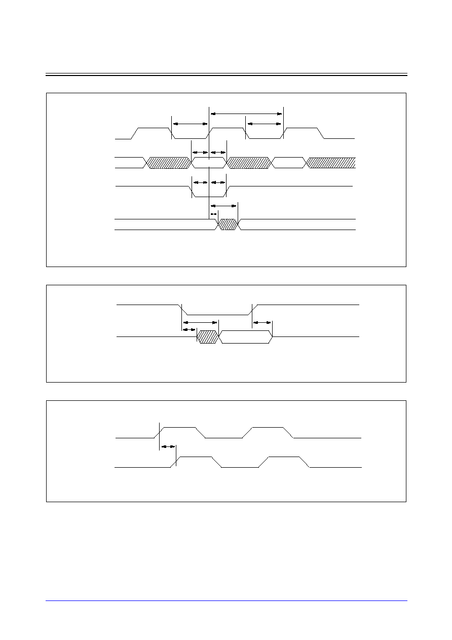
STDL130
5-184
Samsung ASIC
DPSRAMBW_LPL
Low-Power Dual-Port Synchronous Static RAM with Bit-Write
Read Cycle with CSN Controlled
OEN Controlled Output Enable
Contention Mode
NOTE: "don't care" means the condition that these pins are in normal operation mode.
t
as
A [ ]
t
ah
(OEN = low, WEN = high, DI[ ], BWEN[ ] = don't care)
CSN
t
cs
t
ch
DOUT [ ]
t
cyc
CK
t
ckl
t
ckh
A0
A2
A1
t
da
t
acc
M[A1]
M[A0]
(CSN = low, CK, A[ ], WEN, DI[ ], BWEN[ ] = don't care)
t
od
t
dz
Hi-Z
Valid
OEN
DOUT [ ]
Hi-Z
t
zd
CK1
tcc
CK2
(A1[ ] = A2[ ])
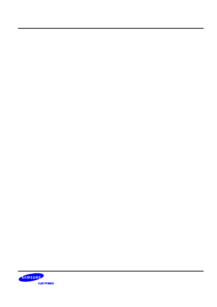
PLL2099X
0.18
µ
µ
m 20MHZ ~ 300MHZ FSPLL
1
GENERAL DESCRIPTION
The pll299x is a Phase-Locked Loop (PLL) frequency synthesizer constructed in CMOS on single monolithic
structure. The PLL macro-functions provide frequency multiplication capabilities. The output clock frequency
FOUT is related to the input clock frequency FIN by the following equation:
FOUT = (m
◊
◊
FIN) / (p
◊
◊
2
S
)
Where, FOUT is the output clock frequency. FIN is the input clock frequency. m, p and s are the values for
programmable dividers. pll2099x consists of a Phase/Frequency Detector(PFD), a Charge Pump, an Internal
Loop Filter, a Voltage Controlled Oscillator(VCO), a 6-bit Pre-divider, an 8-bit Main divider and 2-bit Post Scaler
as shown in Functional Block Diagram.
FEATURES
--
0.18um CMOS device technology
-- 1.8V single power supply
-- Output
frequency range: 20 ~ 300 MHz
-- Jitter
±
120ps at 300MHz
-- Duty ratio 45% to 55% (All tuned range)
-- Frequency changed by programmable divider
-- Power down mode
NOTES
1. Don't set the P or M as zero, that is 000000 / 00000000
2. The proper range of P and M : 1
P
62, 1
M
248
3. The P and M must be selected considering stability of PLL and VCO output frequency range
4. Please consult with SEC application engineer to select the proper P, M and S values
No responsibility is assumed by SEC for its use nor for any infringements of patents or other rights of
third parties that may result from its use. The contents of the datasheet is subject to change without any
notice.
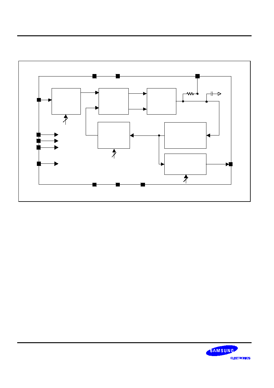
0.18
µ
µ
m 20MHZ ~ 300MHZ FSPLL
PLL2099X
2
FUNCTIONAL BLOCK DIAGRAM
Filter
UP
DN
R1
FOUT
FIN
PWD
P[5:0]
Phase
Frequency
Detector
Charge
Pump
Voltage
Controlled
Oscillator
Main-Divider
(M)
Post -Scaler
(S)
(1,2,4,8)
Fvco/M
Fin/P
Vctrl
Pre-Divider
(P)
Fvco
6b
AVDD18D
AVSS18D
AVDD18A
AVSS18A
VABB
M[7:0]
S[1:0]
8b
2b
C2
PLL2099X
0.18
µ
µ
m 20MHZ ~ 300MHZ FSPLL
3
CORE PIN DESCRIPTION
Pin Name
I/O Type
Pin Description
AVDD18D
DP
Digital power supply
AVSS18D
DG
Digital ground
AVDD18A
AP
Analog power supply
AVSS18A
AG
Analog ground
VABB
AB/DB
Bulk ground
FIN
DI
Reference frequency input
FILTER
AO
Pump out is connected to filter
A capacitor is connected between the pin and analog ground
FOUT
DO
20MHz ~ 300MHz clock output
PWD
DI
FSPLL clock power down.
- When PWD is High, PLL do not operate.
- If customer don't use this pin, apply it to AVSS18D
P[5:0]
DI
The values for 6-bit programmable pre-divider.
M[7:0]
DI
The values for 8-bit programmable main divider.
S[1:0]
DI
The values for 2-bit programmable post scaler.
I/O Type Abbr.
-- AI: Analog Input
-- DI: Digital Input
-- AO: Analog Output
-- DO: Digital Output
-- AB: Analog Bi-direction
-- DB: Digital Bi-direction
-- AP: Analog Power
-- AG: Analog Ground
-- DP: Digital Power
-- DG: Digital Ground
-- BD: Bi-directional Port

0.18
µ
µ
m 20MHZ ~ 300MHZ FSPLL
PLL2099X
4
CORE CONFIGURATION
pll2099x
M[7:0]
S[1:0]
P[5:0]
P[0]
M[5]
M[4]
M[3]
M[2]
M[1]
M[0]
S[1]
S[0]
P[5]
P[4]
P[3]
P[2]
P[1]
M[6]
M[7]
FIN
PWD
FOUT
FILTER
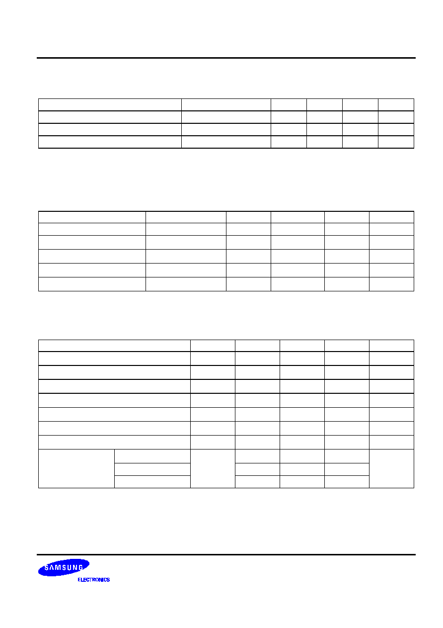
PLL2099X
0.18
µ
µ
m 20MHZ ~ 300MHZ FSPLL
5
RECOMMENDED OPERATING CONDITIONS
Characteristics
Symbol
Min
Typ
Max
Unit
Supply voltage differential
AVDD18D-AVDD18A
≠0.1
+0.1
V
External loop filter capacitance
LF
320
pF
Operating temperature
Topr
≠40
85
∞
C
NOTE: It
is
strongly
recommended
that
all
the
supply
pins
(AVDD18D,
AVDD18A)
be
powered
to
the
same
supply
voltage
to
avoid
power
latch-up.
DC ELECTRICAL CHARACTERISTICS
Characteristics
Symbol
Min
Typ
Max
Unit
Operating voltage
AVDD18D/AVDD18A
1.65
1.8
1.95
V
Digital input voltage high
V
IH
0.7VDD
V
Digital input voltage low
V
IL
0.3VDD
V
Dynamic current
I
dd
3
mA
Power down current
I
pd
40
uA
AC ELECTRICAL CHARACTERISTICS
Characteristics
Symbol
Min
Typ
Max
Unit
Input frequency
F
IN
4
40
MHz
Output clock frequency
F
OUT
20
300
MHz
VCO output frequency
F
VCO
160
400
MHz
Input clock duty cycle
T
ID
40
60
%
Output clock duty cycle (at 300MHz)
T
OD
45
55
%
Input glitch pulse width
T
IGP
1
ns
Locking time
T
LT
150
us
Cycle to cycle jitter
20 ~ 100MHz
T
JCC
≠300
+300
ps
100 ~ 200MHz
≠200
+200
200 ~ 300MHz
≠120
+120
NOTE: It is
strongly
recommended
that
input
signal
is
not
generated
glitch,
but
if
consumer
cannot
help
generating
glitch,
Consumer
must
carefully
considerate
the
specification.
0.18
µ
µ
m 20MHZ ~ 300MHZ FSPLL
PLL2099X
6
FUNCTIONAL DESCRIPTION
A PLL is the circuit synchronizing an output signal (generated by an VCO) with a reference or input signal in
frequency as well as in phase.
The pll2099x can provide frequency multiplication capabilities, but does not
guarantee phase synchronization between FIN and FOUT.
In this application, it includes the following basic blocks.
∑
The voltage-controlled oscillator (VCO) generates VCO output frequency (Fvco) with loop filter DC voltage.
∑
The divider P divides the input frequency by p.
∑
The Main-divider divides the Fvco by m.
∑
The Post-divider divides the Fvco by s and generates FOUT.
∑
The phase frequency detector detects the phase difference between the reference frequency (=FIN/p) and the
feedback frequency (=Fvco/m) and controls the loop filter DC voltage.
∑
The loop filter removes high frequency components and generates stable DC control voltage for VCO.
The m, p, s values can be programmed by 16-bit digital data from the external source. So the PLL can be
locked in the desired frequency.
Fout = m
◊
◊
Fin / p
◊
◊
s (m=M+8 , p=P+2, s=2^S)
Digital data format:
Main Divider
Pre Divider
Post Scaler
M7, M6, M5, M4, M3, M2, M1, M0
P5, P4, P3, P2, P1, P0
S1, S0
NOTE:
S[1] - S[0]: Output Frequency Scaler
M[7] - M[0] : VCO Frequency Divider
P[5] - P[0] : Input Frequency Divider
NOTE
Please contact SEC application engineer to confirm the proper selection of M, P, S values.
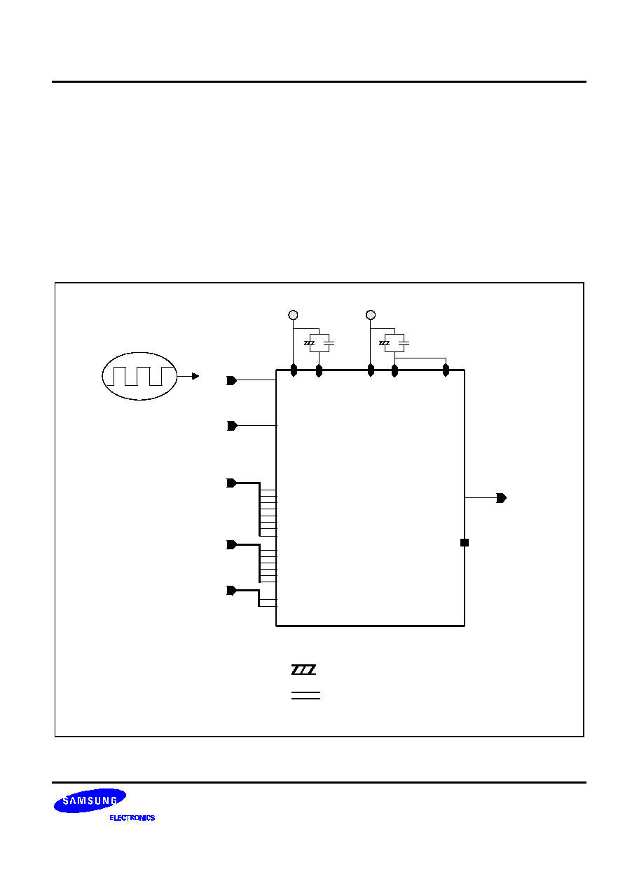
PLL2099X
0.18
µ
µ
m 20MHZ ~ 300MHZ FSPLL
7
CORE EVALUATION GUIDE
1. The FOUT should be bypassed for external test.
2. The pll2099x doesn't contains loop filter (capacitor), so the FILTER is necessarily to be connected to external
pin.
3. You can generate various output frequencies by changing M/P/S setting. There are two methods of
controlling divider values
--
Method 1: 16-bit register can be used for easy control of divider values.
--
Method 2: P, M and S ports are bypassed to the external pin, and you can control each pin directly.
It is undesirable to connect P[5:0], M[7:0] and S[1:0] to the internal power or ground directly
FIN
PWD
FOUT
pll2099x
M[7:0]
P[5:0]
S[1:0]
AVDD18D
AVSS18D
AVDD18A
AVSS18A
VABB
: 10uF ELECTROLYTIC CAPACITOR
UNLESS OTHERWISE SPECIFIED
: 0. 1uF CERAMIC CAPACITOR
UNLESS OTHERWISE SPECIFIED
Filter
0.18
µ
µ
m 20MHZ ~ 300MHZ FSPLL
PLL2099X
8
CORE LAYOUT GUIDE
∑
The digital power(AVDD18D, AVSS18D) and the analog power(AVDD18A, AVSS18A) must be dedicated to
PLL only and separated. If the dedicated AVDD18D and AVSS18D are not allowed, that of the least power
consuming block is shared with the PLL.
∑
The FOUT and FILTER pins must be placed far from the internal signals in order to avoid overlapping signal
lines.
∑
The blocks having a large digital switching current must be located away from the PLL core.
∑
The PLL core must be shielded by guard ring
∑
For the FOUT pad, you can use a custom drive buffer or pot8_lp buffer considering the drive current.
DESIGN CONSIDERATIONS
The following design considerations apply
∑
Jitter is affected by the power noise, substrate noise...etc. It increases when the noise level increases.
∑
A CMOS-level input reference clock is recommend for signal compatibility with the PLL circuit. Other levels
such as TTL may degrade the tolerances.
∑
The use of two, or more PLLs requires special design considerations. Please consult your application
engineer for more information.
∑
The PLL core should be placed as close as possible to the dedicated loop filter and analog power and ground
pins.
∑
It is inadvisable to locate noise-generating signals, such as data buses and high-current outputs, near the PLL
I/O cells.
∑
Other related I/O signals should be placed near the PLL I/O but do not have any pre-defined placement
restriction.
PLL2099X
0.18
µ
µ
m 20MHZ ~ 300MHZ FSPLL
9
PHANTOM CELL INFORMATION
Pins
of the core can be assigned externally(Package Pins) or internally(Internal Ports) depending on design methods.
--
The term "External" implies that the pins should be assigned externally like power pins.
--
The
term "Internal/External" implies that these pins are user dependent.
pll2099x
FILTER
AVDD18A:P
VABB:G
AVSS18A:G
AVDD18D:P
AVSS18D:G
VABB:G
FOUT
S1
S0
M6
M1
M5
M7
PWD
M4
M3
M2
M0
P4
P1
P3
P2
P5
FIN
P0
0.18
µ
µ
m 20MHZ ~ 300MHZ FSPLL
PLL2099X
10
PIN LAYOUT GUIDE
Pin Name
Pin Usage
Pin Layout Guide
AVDD18D
External
Use dedicated power/ground pins for PLL
AVSS18D
External
Power cuts are required to provide on-chip isolation
AVDD18A
External
=> between dedicated PLL power/ground and all other power/ground
AVSS18A
External
Use good power and ground source on board
VABB
External
FIN
External
Do not place noisy, high frequency and high power consuming circuitry
pads near the FIN.
Use proper low jitters reference clock
FOUT
External/Internal
Do not place noisy, high frequency and high power consuming circuitry
pads near the FOUT.
Internal routing path should be short. This will minimize loading effect.
FOUT signals should not be crossed by any signals and should not run
next to digital signals.
This will minimize capacitive coupling between the two signals.
FILTER
External
Do not place noisy, high frequency and high power consuming circuitry
pads near the FILTER.
Ground shielding is needed for internal routing path.
FILTER routing path should not be crossed by any signals and should
not run next to digital signals.
External loop filter pin should be placed between analog power and
ground to avoid stray coupling outside the chip and magnetic coupling
via bond wires.
Closely placed Loop Filter components.
PWD
Internal/External
M[7]~M[0]
Internal/External
P[5]~P[0]
Internal/External
S[1]~S[0]
Internal/External
PLL2099X
0.18
µ
µ
m 20MHZ ~ 300MHZ FSPLL
11
FEEDBACK REQUEST
Thank you for having an interest in our products. Please fill out this form, especially the items which you want to
request.
Parameter
Customer
SEC
Unit
Process
0.18um CMOS
Supply voltage (VDD)
1.8
±
0.15
V
Input frequency (FIN)
4 ~ 40
MHz
Output frequency (FOUT)
20 ~ 300
MHz
Cycle to cycle jitter (TJCC)
20M ~ 100M
±
300
psec (pk-pk)
100M ~ 200M
±
200
200M ~ 300M
±
120
Period jitter (TJP)
20M ~ 100M
±
300
psec (pk-pk)
100M ~ 200M
±
200
200M ~ 300M
±
120
Output duty ratio (TOD)
45 ~ 55
%
Lock up time (TLT)
150
usec
Dynamic current
< 3m
A
Stand by current
< 40u
A
Filter capacitor
External
≠
1. How many PLLs are embedded in your system?
2. Do you need synchronization between input clock and output clock?
3. Do you need another spec of jitter?
Parameter
Customer
Unit
Long-term Jitter (TJLT)
psec (pk-pk)
Tracking Jitter (TJT)
psec (pk-pk)
If you have another special request, please describe below.
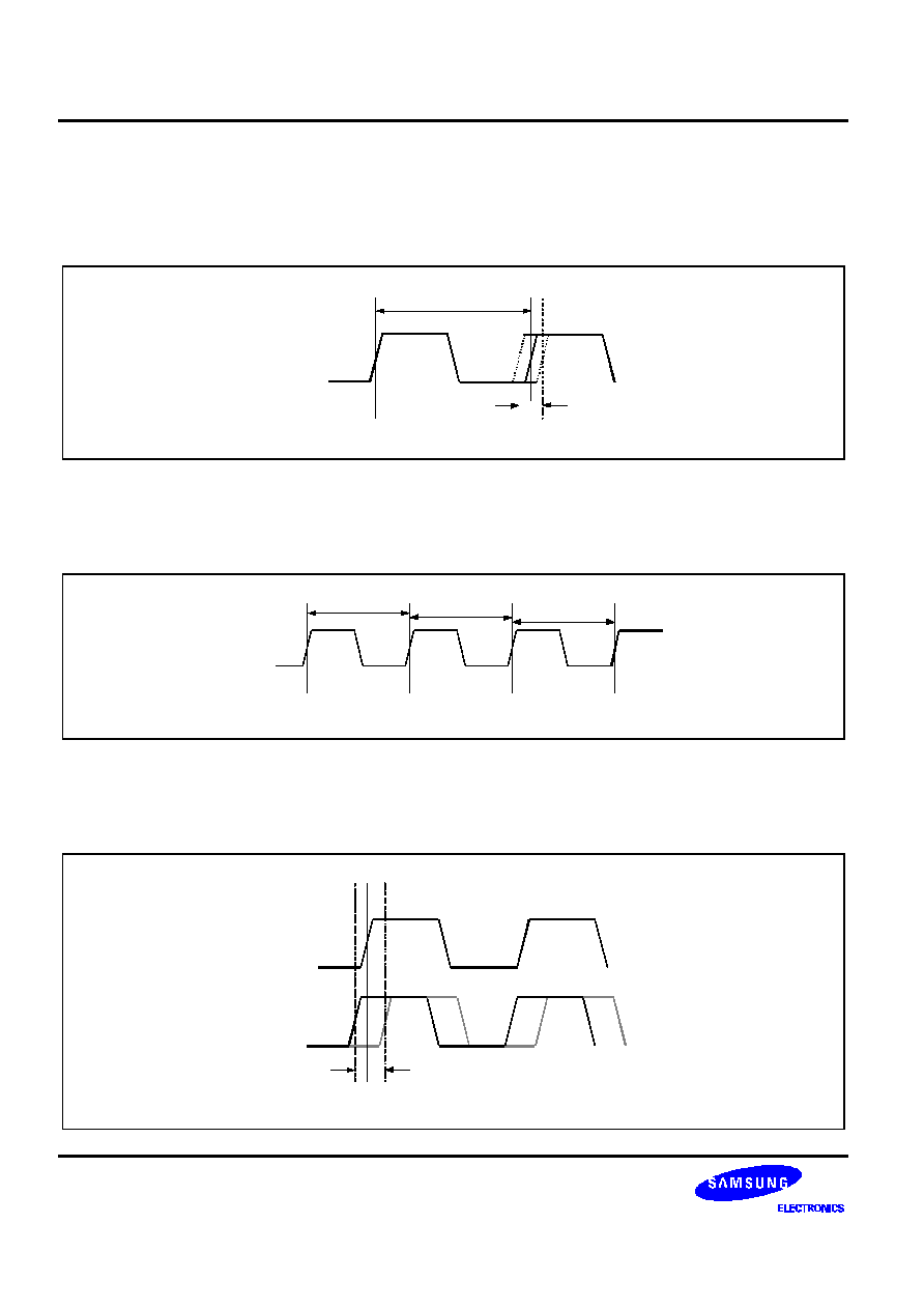
0.18
µ
µ
m 20MHZ ~ 300MHZ FSPLL
PLL2099X
12
JITTER DEFINITION
Period Jitter
Period jitter is the maximum deviation of output clock's transition from its ideal position.
TJP
T
1
Ideal Cycle
FOUT
Cycle-to-Cycle Jitter
Cycle-to-cycle jitter is the maximum deviation of output clock's transition from its corresponding position of the
previous cycle.
FOUT
T
i
T
i+1
T
i-1
TJCC = max(T
i+1
-T
i
)
Long-Term Jitter
Long-term jitter is the maximum deviation of output clock's transition from its ideal position, after many cycles.
The term "many" depends on the application and the frequency.
Cycle 0
Cycle N
TJLP

PLL2099X
0.18
µ
µ
m 20MHZ ~ 300MHZ FSPLL
13
Tracking Jitter
Tracking jitter is the maximum deviation of output clock(FOUT)'s transition from input clock (FIN) position
TJT
Trigger
FIN
FOUT
delay

A
Appendix
Glossary of Analog Terms
Digital-to-Analog Converter
Appendix A
STDL130
A-1
Samsung ASIC
Digital-to-Analog
Converter
1. Resolution - An n-bit binary converter should be able to provide 2
n
distinct and
different analog output values corresponding to the set of n-bit binary words. A
converter that satisfies this criterion is said to have resolution of n bits. The
smallest output change that can be resolved by a linear DAC is 2
-n
of the full-scale
span.
2. Accuracy - Error of a DAC is the difference between the actual analog output
and the output that is expected when a given digital code is applied to the
converter. Source of error include gain error, offset error, linearity error and noise.
Error is usually commensurate with resolution, less than 2
-(n+1)
, or 1/2 LSB of full
scale.
Figure 1-1.
Error of DAC
3. LSB (Least-Significant Bit) - In a system in which a numerical magnitude is
represented by a series of binary digits, the LSB is that bit that carries the smallest
value or weight. It represents the smallest analog change that can be resolved by
an n-bit converter.
LSB (Analog Value) = FSR/2
n
FSR = Full-Scale Range, n = number of bits
4. MSB (Most-Significant Bit) - The binary digit with the largest numerical
weighting. Normally, the MSB of a digital word has a weighting of 1/2 the full
range.
5. Compliance-Voltage Range - For a current output DAC, the maximum range
of(output) terminal voltage for which the device will provide the specified current-
output characteristics.
6. Glitch - A glitch is a switching transient appearing in the output during a code
transition. Its value is expressed as a product of voltage (V
◊
ns) or current (mA
◊
ns) and time duration or charge transferred.
7. Harmonic Distortion (and Total Harmonic Distortion) - The DAC is driven
by the digitized representation of sine wave. The ratio of the RMS sum of the
harmonics of the DAC output to the fundamental value is the THD. Usually only
the lower order harmonics are included, such as second through fifth.
V1: RMS amplitude of the fundamental
8. Signal-to-Noise Ratio (SNR) - This signal to noise ratio depends on the
resolution of the converter and automatically includes specifications of linearity,
distortion, sampling time uncertainty, glitches, noise, and settling time. Over half
Offset Error
Ideal
Actual
Analog
Output
Digital Input
Analog
Output
Digital Input
Ideal
Actual
Gain Error
THD
20
V2
2
V3
2
V4
2
V5
2
+
+
+
(
)
1 2
/
V1
-------------------------------------------------------------------
log
=
Appendix A
Digital-to-Analog Converter
Samsung ASIC
A-2
STDL130
the sampling frequency, this signal to noise ratio must be specified and should
ideally follows the theoretical formula;
S/N
max
= 6.02N + 1.76dB
9. Slew Rate - Slew rate of a device or circuit is a limitation in the rate of change
of output voltage, usually imposed by some basic circuit consideration such as
limited current to charge of capacitor. Amplifiers with slew rate of a few V/
µ
s are
common and moderate in cost. Slew rates greater than about 75V/
µ
s are usually
seen only in more sophisticated (and expensive) devices. The output slewing
speed of a voltage-output DAC is usually limited by the slew rate of the amplifier
used at its output (if one is used).
10. Settling Time - The time required, following a prescribed data change from
the 50% point of the login input change, for the output of a DAC to reach and to
remain within a given fraction (usually
±
1/2LSB) of the final value. Typical pre-
scribed changes are full scale, 1MSB and 1LSB at a major carry. Settling time of
current-output DAC is quite fast. The major share of settling time of a voltage-out-
put DAC is usually contributed by the settling time of the output op-amp circuit.
Figure 1-2.
Setting Time
11. Power-Supply Sensitivity -The sensitivity of a converter to changes in the
power-supply voltages is normally expressed in terms of percent-of-full-scale
change in analog output value (of fractions of 1LSB) for a 1% DC change in the
power supply. Power supply sensitivity may be also expressed in relation to the
specified DC shift of supply voltage. A converter may be considered "good" if the
change in reading at full scale does not exceed 1/2LSB for 3% change in power
supply. Even better specifications are necessary for converters designed for
battery operation.
12. INL (Integral Non Linearity) - Linearity error of a converter, expressed in %,
ppm of full-scale range or multiples of 1LSB, is a deviation of the analog values
in a plot of the measured conversion relationship from a straight line. The straight
line can be either a "best straight line" determined empirically by manipulation of
the gain and/or offset to equalize maximum positive and negative deviation of the
actual transfer characteristics from this straight line; or it can be a straight line
passing through the endpoints of the transfer characteristic after they have been
calibrated (sometimes referred to as "endpoint" linearity). Endpoint linearity error
is similar to relative accuracy error. For multiplying DAC, the analog linearity error,
at a specified digital code, is defined in the same way as for multipliers, by
deviation from a "best straight line" through the plot of the analog output-input
response.
Final Setting
V
0
+
V
0
1
Slewing
Setting Time to
V
0
-
V
0
Slew Rate

Digital-to-Analog Converter
Appendix A
STDL130
A-3
Samsung ASIC
13. DNL (Differential Non Linearity) - Any two adjacent digital codes should re-
sult in measured output values that are exactly 1LSB apart (2
n
of full scale for an
n-bit converter). Any deviation of the measured "step" from the ideal difference is
called differential linearity error expressed in multiplies of 1LSB. It is an important
specification because a differential linearity error greater than 1LSB can lead to
non-monotonic response in a DAC and missed codes in an ADC.
14. Monotonic - A DAC is said to be monotonic if the output either increases or
remains constant as the digital input increases with the result that the output will
always be a single-valued function of the input. The specification "monotonic"
(over a given temperature range) is sometimes substituted for a differential
nonlinearity specification since differential nonlinearity less than 1LSB is a suffi-
cient condition for monotonic behaviour.
2. Analog-to-Digital Converter
1. INL (Integral Non Linearity) - Integral nonlinearity refers to the deviation of
each individual code from a line drawn from "zero" through "full scale". The point
used as "zero" occurs for an analog value 1/2LSB before the first code transition.
"Full scale" is defined as a level 1/2LSB beyond the last code transition. The
deviation is measured from the center of each particular code to the true straight
line.
2. DNL (Differential Non Linearity) - An ideal ADC exhibits code transitions that
are exactly 1LSB apart. DNL is the deviation from this ideal value. It is often
specified in terms of the resolution for which no missing codes are guaranteed.
3. Offset Error - The first transition should occur at a level "zero". Offset is
defined as the deviation of the actual first code transition from that point.
4. Gain Error - The first code transition should occur for an analog value of
nominal negative full scale. The last transition should occur for an analog value
1LSB below the nominal positive full scale. Gain error is the deviation of the actual
difference between first and last code transitions and the ideal difference between
the first and last code transitions.
5. Pipeline Delay (Latency) - The number of clock cycles between conversion
initiation and the associated output data being made available. New output data
is provided every clock cycle.
6. Effective Number of Bits (ENOB) - This is a measure of a device's dynamic
performance and may be obtained from the SNDR or from a sine wave curve test
fit according to the following expression:
ENOB = SNDR - 1.76/6.02
ENOB = N-log2[RMS error (actual) / RMS error (ideal)]
7. Analog Bandwidth - The analog input frequency at which the spectral power
of the fundamental frequency, as determined by FFT analysis is reduced by 3dB.
8. Aperture Delay - The delay between the sampling clock and the instant the
analog input signal is sampled.
9. Aperture Jitter - The sample to sample variation in aperture delay.
Appendix A
Digital-to-Analog Converter
Samsung ASIC
A-4
STDL130
10. Bit Error Rate (BER) - The number of spurious code errors produced for any
given input sine wave frequency at a given clock frequency. In this case it is the
number of codes occurring outside the histogram cusp for a 1/2 FS sine wave.
11. Signal to Noise Ratio - This signal to noise ratio depends on the resolution
of the converter and automatically includes specifications of linearity, distortion,
sampling time uncertainty, glitches, noise, and settling time. Over half the
sampling frequency, this signal to noise ratio must be specified and should ideally
follow the theoretical formula;
S/N
max
= 6.02N + 1.76dB
3. Phase Locked Loop
1. Lock Time - The time it takes the PLL to lock onto the system clock. Fast or
slow lock time may be controlled by the loop filter characteristics. The loop filter
characteristics are controlled by varying the R and C components. (Remember
that R and C define the damping-factor as well)
2. Phase Error - The phase difference between the feedback and the system
clock signal.
3. Clock Jitter - The deviations in a clock's output transitions from their ideal
positions define the clock jitter. Jitter is sometimes specified as an absolute value
in nanoseconds. All jitter measurement are made at a specified voltage.
1) Cycle-to-Cycle Jitter: The change in a clock's output transition from its
corresponding position in the previous cycle. This kind of jitter is the most difficult
to measure and usually requires a time-interval analyzer.
Figure 1-3.
Cycle-to-Cycle Jitter
The maximum of such values over multiple cycles (J1, J2...) is the max. cycle-to-
cycle jitter.
2) Period Jitter: Period jitter measures the maximum change in a clock's output
transition from its ideal position. You can use period jitter measurements to
calculate timing margins in systems.
Clock
t1
t2
t3
Noise:
jitter J1 = t2
-
t1
jitter J2 = t3
-
t2
Digital-to-Analog Converter
Appendix A
STDL130
A-5
Samsung ASIC
Figure 1-4.
Period Jitter
3) Long-Term Jitter: Long-term jitter measures the maximum change in a clock's
output transition from its ideal position over many cycles. How many cycles
depend on the application and the frequency. A classic example of system
affected by long-term jitter is a graphics card driving a CRT.
4) Power Down Mode: PLL state in which the quiescent current is lowered to a
very low level to conserve power.
5) Synthesize Clock: A system clock may run at a relatively low rate compared to
system components. A CPU, for example, may require an internal clock that is
several times faster than the system I/O bus clock. Designers can use PLL
technology to synthesize a higher frequency on-chip clock using the system clock
as a reference.
6) Deskew Clock: Multiple chips on a printed circuit board or cores of different
sizes within a single system on a chip experience clock skew. By using PLL or
DLL technology to shift the phase of the reference clock within each chip or core,
designers can minimize skew tune a system to perform up its potential.
7) Duty Ratio: The percentage of the period that the output is in a high state.
8) Output Frequency Range: The maximum output frequency range minus the
minimum output frequency that is produced with an input signal for which the cell
specifications still apply.
Clock
Ideal Cycle: t1
Jitter

B
Appendix
Timings

Equivalent Standard loads for 4-layer and 5-layer Metal Interconnect
Appendix B
STDL130
B-1
Samsung ASIC
Equivalent Standard loads for 4-layer and 5-layer Metal Interconnect
Gate
Count
Fanouts
1
2
3
4
5
6
7
8
16
32
64
4LM
5000
0.795
1.635
2.297
3.204
3.840
4.702
5.263
7.047
10.096
17.588
34.192
10000
0.893
2.015
2.840
4.104
4.907
5.976
6.893
8.326
11.992
20.442
40.696
50000
1.224
2.517
3.533
5.909
7.234
8.277
10.830
11.748
14.370
22.346
43.582
100000
1.374
2.799
4.370
6.312
7.549
9.194
12.147
12.744
16.594
24.009
48.909
150000
4.104
6.291
8.021
10.181
11.003
12.494
13.385
14.358
18.222
26.590
51.212
200000
7.429
8.427
9.480
10.929
12.000
13.362
14.297
15.116
19.155
28.159
53.340
300000
8.171
8.952
10.427
12.165
13.326
14.814
15.836
16.726
21.169
31.078
56.183
400000
8.915
10.269
11.297
13.127
14.413
16.045
17.169
18.102
22.883
33.533
59.104
500000
9.944
12.015
12.690
14.722
16.147
17.962
19.210
20.299
24.356
35.700
63.417
600000
10.647
12.681
13.663
15.828
17.344
19.285
20.616
21.822
25.055
36.732
67.431
800000
12.267
15.511
15.875
18.354
20.086
22.314
23.840
25.305
27.076
39.708
75.316
1000000
13.781
16.214
17.944
20.712
22.649
25.145
26.854
28.559
28.954
42.474
78.842
1500000
17.931
21.675
23.578
27.149
29.643
32.879
35.088
37.435
41.425
50.795
95.393
2000000
21.816
26.935
28.858
33.181
36.200
40.127
42.803
45.751
53.533
58.578
106.937
2500000
25.456
32.411
33.799
38.826
42.344
46.911
50.027
53.535
58.472
65.850
123.366
3000000
28.856
35.562
38.419
44.106
48.068
53.251
56.775
60.812
63.080
72.631
138.822
4000000
33.106
39.990
44.076
50.600
55.145
61.094
65.137
69.767
75.133
83.328
158.169
5000000
37.122
48.001
49.423
56.736
61.836
68.503
73.039
76.259
77.242
93.437
166.500
6000000
41.625
52.812
55.417
63.620
69.338
76.812
81.899
87.718
91.773
104.769
196.954
5LM
5000
0.755
1.553
2.183
3.045
3.647
4.468
5.000
6.694
9.592
16.708
32.482
10000
0.848
1.915
2.698
3.899
4.661
5.677
6.549
7.909
11.391
19.421
38.661
50000
1.163
2.391
3.356
5.614
6.872
7.864
10.289
11.161
13.651
21.228
41.403
100000
1.305
2.659
4.151
5.998
7.171
8.734
11.539
12.106
15.763
22.809
46.464
150000
3.899
5.976
7.620
9.671
10.452
11.870
12.716
13.639
17.311
25.261
48.651
200000
7.057
8.005
9.005
10.381
11.399
12.694
13.582
14.360
18.196
26.751
50.673
300000
7.761
8.505
9.905
11.557
12.659
14.074
15.045
15.889
20.110
29.525
53.374
400000
8.470
9.755
10.732
12.472
13.692
15.242
16.311
17.196
21.740
31.856
56.149
500000
9.446
11.415
12.057
13.986
15.340
17.064
18.250
19.283
23.137
33.915
60.246
600000
10.116
12.047
12.980
15.037
16.476
18.320
19.584
20.732
23.803
34.895
64.059
800000
11.653
14.736
15.082
17.437
19.082
21.198
22.647
24.039
25.722
37.722
71.551
1000000
13.092
15.403
17.047
19.677
21.517
23.887
25.511
27.131
27.507
40.350
74.899
1500000
17.035
20.590
22.399
25.791
28.161
31.236
33.334
35.562
39.354
48.255
90.624
2000000
20.726
25.588
27.415
31.521
34.389
38.122
40.663
43.464
50.856
55.649
101.590
2500000
24.183
30.791
32.108
36.885
40.218
44.564
47.525
50.858
55.549
62.557
117.198
3000000
27.413
33.785
36.498
41.901
45.665
50.588
53.937
57.771
59.927
69.000
131.881
4000000
31.450
37.990
41.872
48.070
52.387
58.039
61.879
66.279
71.377
79.161
150.259
5000000
35.265
45.602
46.952
53.899
58.744
65.078
69.387
74.316
73.379
88.765
158.175
6000000
39.545
50.173
52.645
60.438
65.872
72.972
77.805
83.332
87.185
99.531
187.106
7000000
43.045
60.980
65.492
72.098
76.480
81.466
86.862
96.755
101.602
123.818
246.722
8000000
48.265
68.374
73.437
80.842
85.755
91.350
97.397
108.492
113.482
138.836
251.716
Appendix B
Equivalent Standard loads for 6-layer Metal Interconnect
Samsung ASIC
B-2
STDL130
Equivalent Standard loads for 6-layer Metal Interconnect
Gate
Count
Fanouts
1
2
3
4
5
6
7
8
16
32
64
6LM
5000
0.716
1.472
2.066
2.883
3.456
4.232
4.738
6.342
9.086
15.830
30.773
10000
0.805
1.814
2.557
3.694
4.417
5.377
6.204
7.494
10.793
18.399
36.627
50000
1.102
2.265
3.181
5.318
6.511
7.448
9.748
10.572
12.933
20.112
39.224
100000
1.236
2.519
3.933
5.681
6.795
8.275
10.933
11.470
14.935
21.608
44.017
150000
3.694
5.661
7.218
9.163
9.903
11.244
12.047
12.923
16.399
23.931
46.090
200000
6.687
7.584
8.531
9.836
10.799
12.025
12.868
13.604
17.240
25.344
48.005
300000
7.354
8.057
9.383
10.948
11.994
13.332
14.251
15.053
19.053
27.970
50.564
400000
8.023
9.242
10.167
11.814
12.972
14.440
15.452
16.291
20.596
30.181
53.194
500000
8.950
10.814
11.421
13.250
14.533
16.167
17.289
18.269
21.921
32.129
57.074
600000
9.582
11.413
12.297
14.246
15.610
17.356
18.555
19.639
22.549
33.059
60.688
800000
11.041
13.960
14.287
16.519
18.078
20.082
21.456
22.775
24.370
35.738
67.785
1000000
12.403
14.592
16.149
18.641
20.383
22.631
24.169
25.702
26.059
38.226
70.958
1500000
16.137
19.507
21.220
24.435
26.679
29.592
31.578
33.690
37.283
45.716
85.854
2000000
19.635
24.242
25.972
29.862
32.580
36.116
38.523
41.177
48.181
52.720
96.244
2500000
22.911
29.169
30.419
34.944
38.100
42.220
45.025
48.181
52.625
59.265
111.029
3000000
25.970
32.005
34.576
39.694
43.261
47.927
51.098
54.732
56.773
65.368
124.940
4000000
29.795
35.990
39.669
45.539
49.631
54.984
58.624
62.791
67.620
74.996
142.352
5000000
33.409
43.202
44.480
51.062
55.653
61.653
65.736
68.437
69.517
84.092
149.850
6000000
37.462
47.531
49.875
57.257
62.405
69.131
73.708
78.946
82.596
94.293
177.259
7000000
40.779
57.769
62.045
68.303
72.454
77.179
82.289
91.663
96.253
117.301
233.736
8000000
45.724
64.775
69.570
76.586
81.242
86.541
92.271
102.781
107.509
131.529
238.466

C
Appendix
Maximum Fanouts

Maximum Fanouts of Primitive Cells
Appendix C
STDL130
C-1
Samsung ASIC
Maximum Fanouts of
Primitive Cells
(When input t
R
/t
F
= 0.217ns,
one fanout (SL) = 0.00515pF)
Cell Name
Output
Pin
Maximum
Fanout
ad2_lp
Y
38
ad2b_lp
Y
38
ad2bd2_lp
Y
78
ad2bd4_lp
Y
156
ad2bd8_lp
Y
311
ad2d2_lp
Y
77
ad2d4_lp
Y
155
ad2d8_lp
Y
310
ad3_lp
Y
39
ad3d2_lp
Y
77
ad3d4_lp
Y
152
ad4_lp
Y
39
ad4d2_lp
Y
77
ad4d4_lp
Y
151
ad5_lp
Y
18
ad5d2_lp
Y
36
ad5d4_lp
Y
158
ao21_lp
Y
17
ao211_lp
Y
10
ao2111_lp
Y
6
ao2111d2_lp
Y
78
ao211d2_lp
Y
21
ao211d4_lp
Y
158
ao21d2_lp
Y
34
ao21d4_lp
Y
157
ao22_lp
Y
17
ao221_lp
Y
9
ao221d2_lp
Y
77
ao221d4_lp
Y
157
ao222_lp
Y
9
ao2222_lp
Y
6
ao2222d2_lp
Y
77
ao2222d4_lp
Y
158
ao222a_lp
Y
14
ao222d2_lp
Y
78
ao222d4_lp
Y
158
ao22a_lp
Y
16
ao22d2_lp
Y
33
ao22d4_lp
Y
156
ao31_lp
Y
16
ao311_lp
Y
9
ao3111_lp
Y
5
ao31d2_lp
Y
33
ao31d4_lp
Y
156
ao32_lp
Y
16
ao321_lp
Y
8
ao322_lp
Y
8
ao32d2_lp
Y
78
ao33_lp
Y
15
ao331_lp
Y
8
ao332_lp
Y
8
busholder_lp
Y
10000
cglp_lp
GCK
37
cglpd2_lp
GCK
76
cglpd4_lp
GCK
154
cglp
GCK
38
cglpd2
GCK
78
cglpd4
GCK
156
dl1d2
Y
77
dl2d2
Y
77
dl5d2
Y
78
dl10d2
Y
78
fa_lp
S
39
CO
38
fad2_lp
S
78
CO
78
fd1_lp
Q
38
QN
38
fd1d2_lp
Q
77
QN
77
fd1q_lp
Q
38
fd1qd2_lp
Q
78
fd1s_lp
Q
38
QN
38
fd1sd2_lp
Q
78
QN
78
fd1sq_lp
Q
38
fd1sqd2_lp
Q
78
fd2_lp
Q
38
QN
38
fd2d2_lp
Q
78
QN
78
fd2q_lp
Q
39
fd2qd2_lp
Q
79
fd2s_lp
Q
39
QN
38
fd2sd2_lp
Q
78
QN
78
fd2sq_lp
Q
39
fd2sqd2_lp
Q
79
fd3_lp
Q
38
QN
38
fd3d2_lp
Q
77
QN
77
fd3q_lp
Q
38
fd3qd2_lp
Q
78
fd3s_lp
Q
38
QN
39
fd3sd2_lp
Q
78
QN
79
fd3sq_lp
Q
38
fd3sqd2_lp
Q
78
fd4_lp
Q
39
QN
38
fd4d2_lp
Q
78
QN
77
fd4q_lp
Q
39
fd4qd2_lp
Q
78
fd4s_lp
Q
39
QN
38
fd4sd2_lp
Q
79
QN
77
fd4sq_lp
Q
39
fd4sqd2_lp
Q
79
fd5_lp
Q
38
QN
38
fd5d2_lp
Q
77
QN
77
fd5s_lp
Q
38
QN
38
fd5sd2_lp
Q
78
QN
78
fd6_lp
Q
39
QN
38
fd6d2_lp
Q
78
QN
78
fd6s_lp
Q
39
QN
38
Cell Name
Output
Pin
Maximum
Fanout
Appendix C
Maximum Fanouts of Primitive Cells
Samsung ASIC
C-2
STDL130
fd6sd2_lp
Q
78
QN
78
fd7_lp
Q
38
QN
39
fd7d2_lp
Q
78
QN
79
fd7s_lp
Q
38
QN
39
fd7sd2_lp
Q
78
QN
79
fd8_lp
Q
39
QN
38
fd8d2_lp
Q
79
QN
77
fd8s_lp
Q
39
QN
38
fd8sd2_lp
Q
78
QN
77
fds2_lp
Q
38
QN
38
fds2d2_lp
Q
78
QN
78
fds2s_lp
Q
38
QN
38
fds2sd2_lp
Q
78
QN
78
fds3_lp
Q
38
QN
38
fds3d2_lp
Q
78
QN
78
fds3s_lp
Q
38
QN
38
fds3sd2_lp
Q
78
QN
78
fj2_lp
Q
39
QN
38
fj2d2_lp
Q
79
QN
78
fj2s_lp
Q
39
QN
38
fj2sd2_lp
Q
79
QN
78
fj4_lp
Q
38
QN
39
fj4d2_lp
Q
77
QN
78
fj4s_lp
Q
39
QN
38
fj4sd2_lp
Q
78
QN
77
ft2_lp
Q
39
QN
38
ft2d2_lp
Q
79
QN
78
ha_lp
S
38
CO
38
had2_lp
S
78
CO
77
iv_lp
Y
39
ivd2_lp
Y
81
ivd3_lp
Y
121
ivd4_lp
Y
160
ivd6_lp
Y
242
ivd8_lp
Y
323
ivd16_lp
Y
648
ivd24_lp
Y
968
Cell Name
Output
Pin
Maximum
Fanout
ivt_lp
Y
38
ivtd2_lp
Y
78
ivtd4_lp
Y
157
ivtd8_lp
Y
311
ivtd16_lp
Y
615
ld1_lp
Q
39
QN
38
ld1d2_lp
Q
77
QN
77
ld1q_lp
Q
39
ld1qd2_lp
Q
79
ld2_lp
Q
38
QN
38
ld2d2_lp
Q
77
QN
78
ld2q_lp
Q
39
ld2qd2_lp
Q
78
ld3_lp
Q
38
QN
38
ld3d2_lp
Q
78
QN
78
ld4_lp
Q
38
QN
39
ld4d2_lp
Q
78
QN
78
ld5_lp
Q
38
QN
38
ld5d2_lp
Q
78
QN
79
ld5q_lp
Q
39
ld5qd2_lp
Q
77
ld6_lp
Q
38
QN
38
ld6d2_lp
Q
77
QN
79
ld6q_lp
Q
39
ld6qd2_lp
Q
78
mx2_lp
Y
39
mx2d2_lp
Y
78
mx2d4_lp
Y
158
mx2i_lp
YN
17
mx2ia_lp
YN
17
mx2id2_lp
YN
34
mx2id2a_lp
YN
34
mx2id4_lp
YN
155
mx2id4a_lp
YN
156
mx4_lp
Y
38
mx4d2_lp
Y
77
mx4d4_lp
Y
150
nd2_lp
Y
38
nd2b_lp
Y
38
nd2bd2_lp
Y
77
nd2bd4_lp
Y
153
nd2bd8_lp
Y
312
nd2d2_lp
Y
77
nd2d4_lp
Y
154
nd2d8_lp
Y
309
nd3_lp
Y
26
nd3b_lp
Y
26
nd3bd2_lp
Y
54
nd3bd4_lp
Y
154
nd3bd8_lp
Y
311
nd3d2_lp
Y
54
nd3d4_lp
Y
154
nd3d8_lp
Y
311
nd4_lp
Y
20
Cell Name
Output
Pin
Maximum
Fanout

Maximum Fanouts of Primitive Cells
Appendix C
STDL130
C-3
Samsung ASIC
nd4d2_lp
Y
40
nd4d4_lp
Y
154
nd5_lp
Y
38
nd5d2_lp
Y
77
nd5d4_lp
Y
156
nd6_lp
Y
38
nd6d2_lp
Y
77
nd6d4_lp
Y
156
nd8_lp
Y
38
nd8d2_lp
Y
76
nd8d4_lp
Y
156
nid_lp
Y
38
nid16_lp
Y
619
nid2_lp
Y
78
nid3_lp
Y
116
nid4_lp
Y
156
nid6_lp
Y
234
nid8_lp
Y
311
nid24_lp
Y
936
nit_lp
Y
38
nitd16_lp
Y
612
nitd2_lp
Y
78
nitd4_lp
Y
157
nitd8_lp
Y
311
nr2_lp
Y
18
nr2a_lp
Y
37
nr2b_lp
Y
18
nr2bd2_lp
Y
36
nr2bd4_lp
Y
156
nr2bd8_lp
Y
312
nr2d2_lp
Y
36
nr2d4_lp
Y
156
nr2d8_lp
Y
312
nr3_lp
Y
11
nr3a_lp
Y
23
nr3d2_lp
Y
23
nr3d4_lp
Y
156
nr4_lp
Y
38
nr4d2_lp
Y
78
nr4d4_lp
Y
158
nr5_lp
Y
38
nr5d2_lp
Y
77
nr5d4_lp
Y
156
nr6_lp
Y
38
nr6d2_lp
Y
77
nr6d4_lp
Y
158
nr8_lp
Y
38
nr8d2_lp
Y
77
nr8d4_lp
Y
154
oa21_lp
Y
17
oa211_lp
Y
16
oa2111_lp
Y
17
oa2111d2_lp
Y
33
oa211d2_lp
Y
34
oa211d4_lp
Y
156
oa21d2_lp
Y
35
oa21d4_lp
Y
156
oa22_lp
Y
16
oa221_lp
Y
15
oa221d2_lp
Y
32
oa221d4_lp
Y
156
oa222_lp
Y
14
oa2222_lp
Y
11
oa2222d2_lp
Y
78
oa2222d4_lp
Y
158
oa222d2_lp
Y
30
Cell Name
Output
Pin
Maximum
Fanout
oa222d4_lp
Y
158
oa22a_lp
Y
17
oa22d2_lp
Y
33
oa22d2a_lp
Y
35
oa22d4_lp
Y
157
oa22d4a_lp
Y
156
oa31_lp
Y
11
oa311_lp
Y
10
oa3111_lp
Y
9
oa31d2_lp
Y
22
oa31d4_lp
Y
156
oa32_lp
Y
9
oa321_lp
Y
9
oa322_lp
Y
8
oa33_lp
Y
9
or2_lp
Y
38
or2b_lp
Y
38
or2bd2_lp
Y
77
or2bd4_lp
Y
155
or2bd8_lp
Y
312
or2d2_lp
Y
77
or2d4_lp
Y
155
or2d8_lp
Y
310
or3_lp
Y
38
or3d2_lp
Y
78
or3d4_lp
Y
156
or4_lp
Y
37
or4d2_lp
Y
75
or4d4_lp
Y
155
or5_lp
Y
38
or5d2_lp
Y
76
or5d4_lp
Y
156
scg1_lp
Y
26
scg1d2_lp
Y
53
scg2_lp
Y
38
scg2d2_lp
Y
77
scg2d4_lp
Y
155
scg3_lp
Y
26
scg3d2_lp
Y
53
scg3d4_lp
Y
155
scg4_lp
Y
38
scg4d2_lp
Y
77
scg4d4_lp
Y
152
scg5_lp
Y
37
scg5d2_lp
Y
76
scg5d4_lp
Y
153
scg6_lp
Y
38
scg6d2_lp
Y
78
scg7_lp
Y
38
scg7d2_lp
Y
75
scg8_lp
Y
38
scg8d2_lp
Y
78
scg9_lp
Y
38
scg9d2_lp
Y
79
scg10_lp
Y
38
scg10d2_lp
Y
78
scg11_lp
Y
11
scg11d2_lp
Y
23
scg12_lp
Y
18
scg12d2_lp
Y
36
scg12d4_lp
Y
156
scg13_lp
Y
38
scg13d2_lp
Y
77
scg14_lp
Y
37
scg14d2_lp
Y
76
scg15_lp
Y
26
Cell Name
Output
Pin
Maximum
Fanout
Appendix C
Maximum Fanouts of Primitive Cells
Samsung ASIC
C-4
STDL130
scg15d2_lp
Y
53
scg16_lp
Y
17
scg16d2_lp
Y
35
scg17_lp
Y
37
scg17d2_lp
Y
77
scg18_lp
Y
26
scg18d2_lp
Y
54
scg19_lp
Y
17
scg19d2_lp
Y
34
scg20_lp
Y
18
scg20d2_lp
Y
36
scg21_lp
Y
11
scg21d2_lp
Y
23
scg22_lp
Y
17
scg22d2_lp
Y
35
xn2_lp
Y
39
xn2d2_lp
Y
78
xn2d4_lp
Y
154
xn3_lp
Y
38
xn3d2_lp
Y
75
xn3d4_lp
Y
146
xo2_lp
Y
39
xo2d2_lp
Y
78
xo2d4_lp
Y
155
xo3_lp
Y
37
xo3d2_lp
Y
75
xo3d4_lp
Y
151
Cell Name
Output
Pin
Maximum
Fanout

Maximum Fanouts of I/O Cells
Appendix C
STDL130
C-5
Samsung ASIC
Maximum Fanouts of
I/O Cells
(When input t
R
/t
F
= 0.217ns,
one fanout (SL) = 0.00515pF)
Cell Name
Output
Pin
Maximum
Fanout
phic_lp
Y
166
phic_abb_lp
Y
222
phicc_abb_lp
Y
225
phicd_lp
Y
166
phicd_abb_lp
Y
222
phicen_abb_lp
Y
219
phicu_lp
Y
166
phicu_abb_lp
Y
222
phis_lp
Y
166
phis_abb_lp
Y
217
phisd_lp
Y
166
phisd_abb_lp
Y
217
phisu_lp
Y
166
phisu_abb_lp
Y
217
phsckdc2_lp
Y
552
phsckdc4_lp
Y
1074
phsckdc6_lp
Y
1542
phsckdc8_lp
Y
1946
phsckdcd2_lp
Y
552
phsckdcd4_lp
Y
1074
phsckdcd6_lp
Y
1542
phsckdcd8_lp
Y
1946
phsckdcu2_lp
Y
552
phsckdcu4_lp
Y
1074
phsckdcu6_lp
Y
1542
phsckdcu8_lp
Y
1946
phsckds2_lp
Y
552
phsckds4_lp
Y
1074
phsckds6_lp
Y
1542
phsckds8_lp
Y
1946
phsckdsd2_lp
Y
552
phsckdsd4_lp
Y
1074
phsckdsd6_lp
Y
1542
phsckdsd8_lp
Y
1946
phsckdsu2_lp
Y
552
phsckdsu4_lp
Y
1074
phsckdsu6_lp
Y
1542
phsckdsu8_lp
Y
1946
phtic_lp
Y
166
phticd_lp
Y
166
phticu_lp
Y
166
phtis_lp
Y
166
phtisd_lp
Y
166
phtisu_lp
Y
166
phsosck1_lp
YN
135
phsosck17_lp
YN
135
phsosck2_lp
YN
42
phsosck27_lp
YN
42
phsoscm1_lp
YN
51
phsoscm16_lp
YN
51
phsoscm2_lp
YN
429
phsoscm26_lp
YN
430
phsoscm3_lp
YN
516
phsoscm36_lp
YN
524
pic_lp
Y
253
pic_abb_lp
Y
253
picc_abb_lp
Y
257
picd_lp
Y
253
picd_abb_lp
Y
253
picen_abb_lp
Y
244
picu_lp
Y
252
picu_abb_lp
Y
252
pis_lp
Y
248
pis_abb_lp
Y
248
pisd_lp
Y
248
pisd_abb_lp
Y
248
pisu_lp
Y
248
pisu_abb_lp
Y
248
pmic_lp
Y
106
pmic_abb_lp
Y
171
pmicc_abb_lp
Y
172
pmicd_lp
Y
106
pmicd_abb_lp
Y
170
pmicen_abb_lp
Y
165
pmicu_lp
Y
106
pmicu_abb_lp
Y
168
pmis_lp
Y
106
pmis_abb_lp
Y
168
pmisd_lp
Y
106
pmisd_abb_lp
Y
168
pmisu_lp
Y
106
pmisu_abb_lp
Y
168
pmsckdc2_lp
Y
553
pmsckdc4_lp
Y
1075
pmsckdc6_lp
Y
1545
pmsckdc8_lp
Y
1951
pmsckdcd2_lp
Y
553
pmsckdcd4_lp
Y
1075
pmsckdcd6_lp
Y
1545
pmsckdcd8_lp
Y
1951
pmsckdcu2_lp
Y
553
pmsckdcu4_lp
Y
1075
pmsckdcu6_lp
Y
1545
pmsckdcu8_lp
Y
1951
pmsckds2_lp
Y
553
pmsckds4_lp
Y
1075
pmsckds6_lp
Y
1545
pmsckds8_lp
Y
1951
pmsckdsd2_lp
Y
553
pmsckdsd4_lp
Y
1075
pmsckdsd6_lp
Y
1545
pmsckdsd8_lp
Y
1951
pmsckdsu2_lp
Y
553
pmsckdsu4_lp
Y
1075
pmsckdsu6_lp
Y
1545
pmsckdsu8_lp
Y
1951
pmsosck1_lp
YN
136
pmsosck2_lp
YN
42
pmsoscm1_lp
YN
50
pmsoscm2_lp
YN
206
psckdc2_lp
Y
608
psckdc4_lp
Y
1183
psckdc6_lp
Y
1709
psckdc8_lp
Y
2171
psckdcd2_lp
Y
608
psckdcd4_lp
Y
1184
psckdcd6_lp
Y
1708
psckdcd8_lp
Y
2166
psckdcu2_lp
Y
608
psckdcu4_lp
Y
1182
psckdcu6_lp
Y
1708
psckdcu8_lp
Y
2170
psckds2_lp
Y
603
psckds4_lp
Y
1148
psckds6_lp
Y
1606
psckds8_lp
Y
1971
psckdsd2_lp
Y
603
psckdsd4_lp
Y
1146
psckdsd6_lp
Y
1601
psckdsd8_lp
Y
1962
psckdsu2_lp
Y
603
psckdsu4_lp
Y
1147
psckdsu6_lp
Y
1605
Cell Name
Output
Pin
Maximum
Fanout

Appendix C
Maximum Fanouts of I/O Cells
Samsung ASIC
C-6
STDL130
psckdsu8_lp
Y
1967
psosck1_lp
YN
227
psosck2_lp
YN
231
psoscm1_lp
YN
232
psoscm2_lp
YN
232
ptic_lp
Y
250
pticd_lp
Y
249
pticu_lp
Y
250
ptis_lp
Y
244
ptisd_lp
Y
208
ptisu_lp
Y
244
Cell Name
Output
Pin
Maximum
Fanout
Maximum Fanout for CK and NID Cells
Appendix C
STDL130
C-7
Samsung ASIC
Maximum Fanout for
CK and NID Cells
<Condition>
∑
Library = STDL130
∑
V
DD
= 1.8V
∑
Fanout = 0.00466pF (= input capacitance for CK pin of FD1_LP)
∑
Standard Load (SL) = 0.00515pF
∑
Input slope = 0.217ns
∑
Maximum output transition time (MOTT) = 1.2ns
∑
Maximum frequency
300MHz
∑
Net length (
µ
m/fanout): branch net length for each fanout except trunk
For high fanout nets including clock net, Samsung strongly recommends using
clock tree synthesis.
Trunk width (
µ
m)
8
In case that
interconnection
is not considered
Net length
(
µ
m/fanout)
20
200
Trunk length (
µ
m)
2000
5000
2000
5000
ck2_lp
259
163
60
37
662
ck4_lp
561
434
129
100
1321
ck6_lp
851
674
196
155
1984
ck8_lp
1125
881
259
203
2643
Trunk width (
µ
m)
0.28
8
In case that
interconnection
is not considered
Net length
(
µ
m/fanout)
20
200
Trunk length (
µ
m)
2000
5000
2000
5000
nid_lp
-
-
-
-
38
nid2_lp
17
-
-
-
78
nid3_lp
32
-
-
-
116
nid4_lp
48
-
6
-
156
nid6_lp
74
11
17
-
234
nid8_lp
94
19
27
4
311
nid16_lp
147
33
68
43
619
nid24_lp
173
38
109
80
936

D
Appendix
Package Capabilities
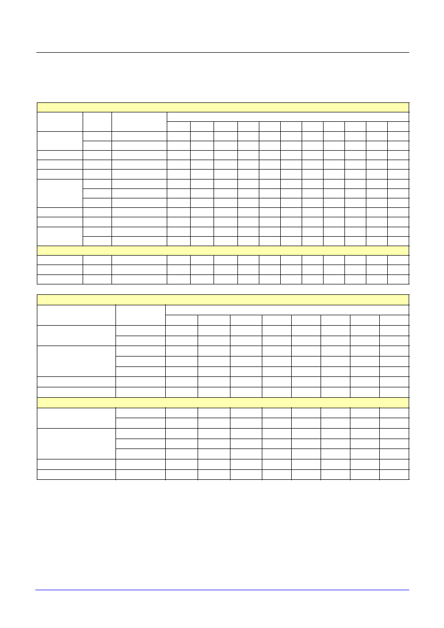
Package
Appendix D
STDL130
D-1
Samsung ASIC
Package
The most current package availability and capability can be obtained from your
local Samsung Technology and Design Centers.
s
In-house
Sub-contractor
LQFP
Package
Pitch
Lead
Inductance
Lead Count
32
48
64
80
100
128
144
160
176
208
256
0707 mm
0.8
s
0.5
< 3nH
s
1010 mm
0.5
< 5nH
s
1212 mm
0.5
< 5nH
s
1420 mm
0.5
< 12nH
s
1414 mm
0.8
< 6nH
s
0.5
< 6nH
s
0.4
v
s
2020 mm
0.4
s
2024 mm
0.5
s
s
2828 mm
0.5
< 17nH
s
0.4
< 17nH
s
TQFP
1212 mm
0.5
< 5nH
s
1414 mm
0.5
< 5nH
s
1420 mm
0.065
< 10nH
s
PQFP (PQ2 Thermally Enhanced)
Package
Pitch
Lead Count
100
120
128
144
160
208
240
304
1420 mm
0.65
0.5
2828 mm
0.8
0.65
0.5
3232 mm
0.5
4040 mm
0.5
QFP (with Heat Spreader)
1420 mm
0.65
s
0.5
2828 mm
0.8
s
0.65
0.5
3232 mm
0.5
4040 mm
0.5
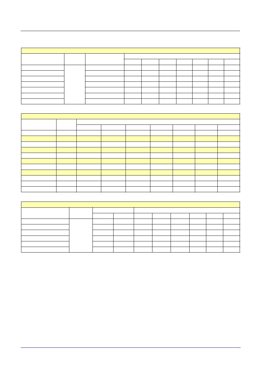
Appendix D
Package
Samsung ASIC
D-2
STDL130
s
In-house
Sub-contractor
PLCC
Package
Pitch
Lead Inductance
Lead Count
18
28
32
44
52
68
84
7.37 x 12.35 mm
1.27
s
11.53 x 11.53 mm
s
11.44 x 13.98 mm
s
16.61 x 16.61 mm
< 5nH
s
19.10 x 19.10 mm
s
24.23 x 24.23 mm
s
29.31 x 29.31 mm
< 13nH
s
SOP
Package
Pitch
Lead Count
32
48
64(56)
68
69
100
256
8.34 x 20.30 mm
1.27
s
TSOP1
1014 mm
0.4
s
PLCC
24.33 x 24.23mm
1.27
s
QFP
1420 mm
0.65
s
FBGA
0909 mm
0.75
s
0911 mm
0.8
s
1717 mm
1.00
s
SBGA
Package
Pitch
Lead Inductance
Lead Count
Lp/g
Lsig
256
304
352
540
648
696
2727 mm
1.27
< 3nH
< 7nH
3131 mm
< 3nH
< 8nH
3535 mm
< 3nH
< 8nH
42.5 x 47.5 mm
< 3nH
<9nH
4545 mm
< 3nH
<9nH
47.5 x 47.5 mm
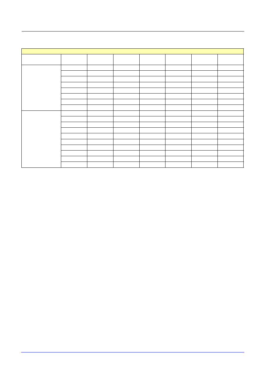
Package
Appendix D
STDL130
D-3
Samsung ASIC
Package Parameter Guide for PBGAs and FBGAs
NOTES: Condition to use above package parameter guide;
1.
Above data are estimated calculations with below assumptions.
2.
Center balls are all ground balls for PBGA ball map design.
3.
For a ball map design, the power/ground ball pair should be arranged next to each other and located on the center closed
inside row and column.
4.
Distance between power/ground bonding pad and ball must be less than listed above T[mm] column distance.
5.
The bonding wire length between power/ground ball and PCB bonding pad should be less than 2mm.
6.
L_total = L_p/g + L_wire; L_p/g: Total inductance of power/ground pad L_sig: Signal line inductance.
7.
Contact IPT development P/T for ball map design request form in special case, other than above 1) ~ 6) notes. Special
guide will be provided.
Lead Inductance
Package Type
Stack-Up
(layer)
PCB Size
(mm x mm)
L_p/g
(nH)
L_wire
(nH)
L_total
(nH)
T
(mm)
L_sig
(nH)
PBGA
2L
23 x 23
< 3.5
1.5
< 4.5
5
< 7
2L
27 x 27
< 4
1.5
< 5.5
6
< 7.5
2L
31 x 31
< 4.1
1.5
< 5.6
7
< 8.5
2L
35 x 35
< 4.5
1.5
< 6
8
< 10
4L
23 x 23
< 1.3
1.5
< 2.8
5
< 3.5
4L
27 x 27
< 1.5
1.5
< 3
6
< 4
4L
31 x 31
< 1.6
1.5
< 3.1
7
< 4.5
4L
35 x 35
< 1.7
1.5
< 3.2
8
< 5.5
FBGA
2L
06 x 06
< 2
1.5
< 3.5
2
< 2.5
2L
08 x 08
< 2
1.5
< 3.5
2
< 3.5
2L
09 x 09
< 2
1.5
< 3.5
2
< 4.5
2L
10 x 10
< 2
1.5
< 3.5
2
< 4.5
2L
12 x 12
< 2
1.5
< 3.5
2
< 5
2L
13 x 13
< 2
1.5
< 3.5
2
< 6
2L
14 x 14
< 2
1.5
< 3.5
2
< 6
2L
16 x 16
< 2
1.5
< 3.5
2
< 7
2L
17 x 17
< 2
1.5
< 3.5
2
< 8
2L
18 x 18
< 2
1.5
< 3.5
2
< 8

Samsung ASIC World Wide Network
S A M S U N G
V
ELECTRONICS
DESIGN CENTERS
SSI
3655 North First Street San Jose CA, 95134,
U.S.A.
TEL
(1)-408-544-4740
FAX
(1)-408-544-4950
SWDC
3345 Michelson Drive, Suite 250, Irvine, CA
92612, U.S.A.
TEL
(1)-408-544-4885
FAX
(1)-408-544-4950
CDI
85 West Tasman Road San Jose, CA 95134
TEL
(1)-408-544-4553
FAX
(1)-408-544-4979
SSEL
Samsung Electronics Europe ASIC Design
Center Great West House, Great West Road,
Brentford, Middlesex TW8 9DQ
TEL
(44)-20-8380-7101
FAX
(44)-20-8380-7095
SoCTechnology
Samsung Electronics Germany ASIC/SOC
Design Center & Sales Representative Am
Kronberger Hang 4, D-65824
Schwalbach/Ts., Germany
TEL
(49)-6196-66-7302
FAX
(49)-6196-66-7366
SJC
Samsung Japan Co. ASIC Design Center
Samsung Tokyo Distribution Center 5F,
2-6-38 Shinonome, Koutou-ku, Tokyo,
135-0062
TEL
(81)-3-5564-2100
FAX
(81)-3-5564-2101
ComSOC
Samsung Electronics Singapore ASIC Design
Center 31 International Business Park,
#04-06 Creative Resource, Singapore
609921
TEL
(65)-6425-2212
FAX
(65)-6425-2022
CoAsia
Samsung Electronics Taiwan ASIC Center 9F,
No. 69, Chou Tze St., Nei hu, Taipei, Taiwan,
R.O.C.
TEL
(886)-2-2658-2020
FAX
(886)-2-8780-0101
Si-Plaza
Unit 2505, 25F, Cosco Tower, 183 Queen's
Road Central, HK
TEL
(852)-2907-6388
FAX
(852)-2907-7188
AlphaChips
San #24, Nongseo-Ri Giheung-Eup,
Yongin-City, Gyunggi-Do, Korea
TEL
(82)-031-209-1800
FAX
(82)-031-209-1819

S A M S U N G
V
ELECTRONICS
CUSTOMER
FEEDBACK
We would appreciate your feedback on this document. Please copy the following
page, add your comments, and fax it to us at the address on the following page.
If appropriate, please also fax copies of any marked-up pages from this
document.
Important: Please include your name, phone number, fax number and company
address so that we may contact you directly for clarification or additional
information.
Thank you for your help in improving the quality of our documents.
Customer Feedback
Reader's Comments
Fax your comments to:
System LSI Business,
ASIC Infra P/J
Fax: (82)-031-209-4920
Please tell us how you rate this document. Please a check mark in the appropriate blank for each category.
Excellent
Good
Average
Fair
Poor
Completeness of information
Clarity of information
Ease of finding information
Technical content
Usefulness of examples and
illustrations
Overall manual
What could we do to improve this document?
_________________________________________________________________________________________
_________________________________________________________________________________________
_________________________________________________________________________________________
_________________________________________________________________________________________
_________________________________________________________________________________________
If you found errors in this document, please specify the error and page number. If appropriate, please fax a
marked-up copy of the page(s).
_________________________________________________________________________________________
_________________________________________________________________________________________
_________________________________________________________________________________________
_________________________________________________________________________________________
Please complete the information below so that we may contact you directly for clarification or additional
information.
Name ___________________________________________________
Date ______________________
Telephone __________________________________
Fax ____________________________________
Title
__________________________________________________________________________________
Department
_______________________________________
Mail Stop __________________________
Company Name _________________________________________________________________________
Street
_________________________________________________________________________________
City, State, Zip ___________________________________________________________________________