
PRELIMINARY
1/4 INCH VGA CIS CAMERA MODULE
SX5433M14X-X0B0
1
SX5433M14X-X0B0
(1/4" VGA CIS Camera Module)
Revision 1.3
May. 2004

PRELIMINARY
SX5433M14X-X0B0
1/4" VGA CIS CAMERA MODULE
2
DOCUMENT TITLE
1/4" Optical Size 640x480 (VGA) CIS Camera Module
REVISION HISTORY
Revision
No. History Draft
Date Remark
0.0
Initial draft
Oct. 18, 2003 Preliminary
0.1
Added module dimension
Nov. 7, 2003 Preliminary
0.2
I2C timing modified
Nov. 13, 2003 Preliminary
1.0
Specification is released
Nov. 25, 2003 Preliminary
(Changed operating current, min MCLK and storage
temperature lower value and added AC characteristics).
1.1
Added ESD sensitivity
Nov. 27, 2003 Preliminary
1.2
Changed product code
Jan. 07, 2004 Preliminary
1.3
Stroke out the register map
(published a new document, `Register Map for 433')
Modified the optical characteristics
May. 4, 2004 Preliminary
This document is a general product description and is subject to change without any notice.
PRELIMINARY
1/4 INCH VGA CIS CAMERA MODULE
SX5433M14X-X0B0
3
INTRODUCTION
SX5433M14X-X0B0 is a fully functional camera module with a built-in lens. A low-noise low-power color
CMOS image sensor, S5K433CA03 and an image signal processor, S5C7322X produce high-quality digital video
output in CCIR656 format at maximum 30 frames per second for full frame readout. With SAMSUNG 0.35
µm
CMOS image sensor process technology which is dedicated to higher sensitivity and lower-dark level compared
to standard CMOS process, and on-chip CDS and 10-bit column ADC circuit embedded, the CMOS image sensor
provides high signal-to-noise ratio with low power consumption. This compact camera system consists of an
image sensor, a signal processor and some passive components packed with IR-cut filter and lens units. The
system works with 2.8V single power supply and a clock. All the functions are controlled with control register
setting through the standard 2-wire serial interface.
FEATURES
-- Optical Size: 1/4 inch
-- Unit Pixel: 5.6
µm X 5.6 µm
-- Effective Resolution: 640X480, VGA
-- 8.5mm X 9.5mm X 6.6mm module size
-- 8-bit CCIR656 (YCrCb) Video Output
-- VGA Output Capability
-- Programmable Gamma Correction
-- Auto White Balance and Auto Exposure Control
-- Horizontal and/or Vertical Mirror Output
-- Standby-Mode for Power Saving
-- Maximum 30 Frame per Second
-- Single Power Supply Voltage: 2.8V
-- I
2
C Type Control Interface
PRELIMINARY
SX5433M14X-X0B0
1/4" VGA CIS CAMERA MODULE
4
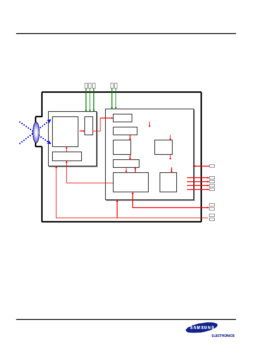
BLOCK DIAGRAM
Pixel Array
640(H) X 480(V)
S5K433CA03
CMOS Image Sensor
S5C7322X
Image Signal Processor
10-bit ADC
Lens Unit
Timing Controller
RISC Processor
(AE, AWB processor)
Line Buffer
Iuminance
Signal
Processor
Pre Processor
Chroma
Signal
Processor
Post Processor
Output
Formatter
STBY
RST
SDA
SCL
VSYNC
HSYNC
PCLK
DATA[0:7]
I2C Bus
MCLK
GNDC
VDDAC
VDDDC
GNDI
VDDDI
PRELIMINARY
1/4 INCH VGA CIS CAMERA MODULE
SX5433M14X-X0B0
5
OPTICAL CHARACTERISTICS
Characteristic
Value
Effective Pixels
640 (H) X 480 (V), VGA
Pixel Size
5.6
µm (H) X 5.6µm (V), square pixel
EFL 3.385mm
F/# 2.8
Diagonal
67.87
∞
Horizontal
56.44
∞
FOV
Vertical
43.59
∞
TV-Distortion -0.33%
Relative Illumination
54.40%
59.90% at 80 lp/mm
Center
72.60% at 50 lp/mm
21.30% at 80 lp/mm
MTF
0.7 Field
42.30% at 50 lp/mm
Lens Construction
All Plastic Lens (2P)
Focus Range
22cm ~
PRELIMINARY
SX5433M14X-X0B0
1/4" VGA CIS CAMERA MODULE
6
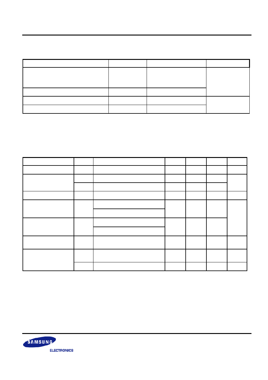
IO PIN DESCRIPTION
(Connector type and pin numbers can be changed as customer's request.)
Module
Pad
Connector
Pin
Pin Name
Type
Notation
1
9
VDDDI
Power
Power supply for signal processor (digital)
2
10
GNDI
Ground
Ground for signal processor
3
15
SCL
In / Out
I
2
C serial communication clock
4
16
SDA
In / Out
I
2
C serial communication data
5
11
RST
In
Reset control (active low)
6
12
STBY
In
Standby mode control (active low)
7
20
MCLK
In
Master input clock
8
17
VSYNC
Out
Vertical synchronization clock
9
18
HSYNC
Out
Horizontal synchronization clock
10
19
PCLK
Out
Pixel output clock
11 8 DATA0 Out
12 7 DATA1 Out
13 6 DATA2 Out
14 5 DATA3 Out
15 4 DATA4 Out
16 3 DATA5 Out
17 2 DATA6 Out
18 1 DATA7 Out
8-bit digital video output
19
13
GNDC
Ground
Ground for sensor circuit block
20
9
VDDCD
Power
Power supply for sensor digital circuit block
21
14
VDDCA
Power
Power supply for sensor analog circuit block
PRELIMINARY
1/4 INCH VGA CIS CAMERA MODULE
SX5433M14X-X0B0
7
MAXIMUM ABSOLUTE RATINGS
Characteristic
Symbol
Rating
Unit
Maximum supply voltage
(VDDDI, VDDAC, VDDC supply
relative to GNDI, GNDC)
V
DD
-0.3 to 3.8
DC Input voltage
V
IN
-0.3 to V
DD
+0.3 (Max. 3.8)
V
Operating temperature
T
OPR
-20 to +60
Storage temperature
T
STG
-40 to +85
∞C
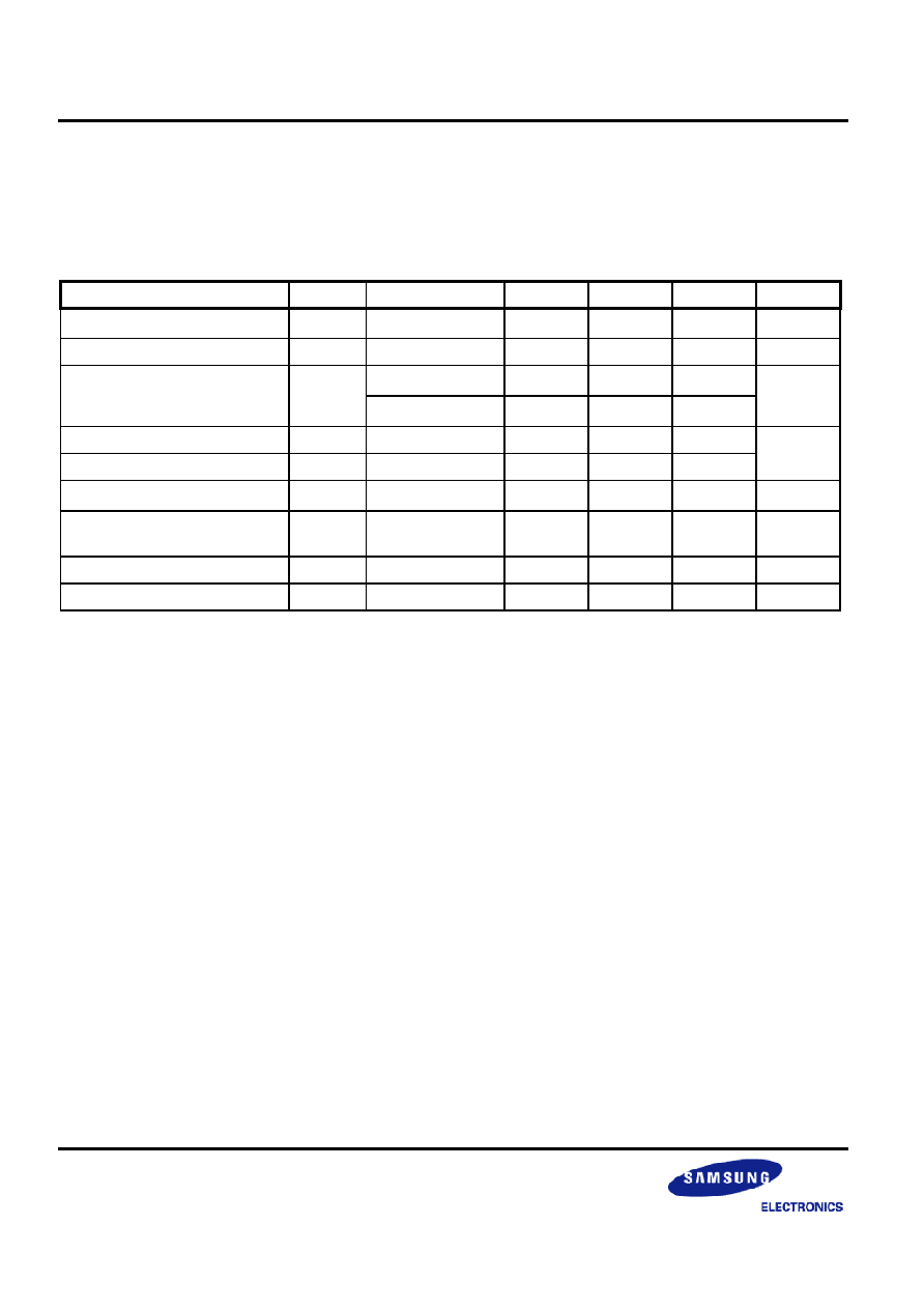
ELECTRICAL CHARACTERISTICS
DC Characteristics
(T
A
= -20 to +60
∞C, C
L
= 15pF)
Characteristics Symbol
Condition
Min Typ Max Unit
Operating voltage
V
DD
VDDDI, VDDAC, VDDC
2.55 2.8 3.05 V
V
IH
-
2.0 - -
Input voltage
(1)
V
IL
-
- - 0.8
V
Input leakage current
(1)
I
IL
V
IN
= V
DD
to V
SS
-10 - 10
µA
I
OH
= -4mA
(2)
High Level Output
voltage
V
OH
I
OH
= -8mA
(3)
0.8V
DD
- -
I
OL
= 4mA
(2)
Low Level Output
voltage
V
OL
I
OL
= 8mA
(3)
- -
0.2V
DD
V
High-Z output leakage
current
(4)
I
OZ
V
OUT
= V
DD
- - 10
µA
I
STB
STBYN = Low (active)
All input clocks = Low
-
15 -
µA
Supply current
I
DD
f
MCLK
= 13.5MHz, 15 fps
- 31 36
mA
NOTES:
1. MCLK, RST, STBY, SCL, and SDA pin.
2. HSYNC, VSYNC, SCL, and SDA pin
3. PCLK, DATA0 to DATA7 pin
4. SCL and SDA pin when in High-Z output state
PRELIMINARY
SX5433M14X-X0B0
1/4" VGA CIS CAMERA MODULE
8
Sensor Imaging Characteristics
(Light source with 3200K of color temperature and IR cut filter (CM-500S, 1mm thickness) is used. Electrical
operating conditions follow the recommended typical values. The control registers are set to the default values.
The ambient temperature, T
A
is 25
∞C if not specified.)
NOTES:
1. Measured minimum output level at 100lux illumination for exposure time 1/30 sec. 7X7 rank filter is applied for the whole
pixel area to eliminate the values from defective pixels.
2. Measured average output at 25% of saturation level illumination for exposure time 1/30 sec. Green channel output values
are used for color version.
3. Measured average output at zero illumination without any offset compensation for exposure time 1/30 sec.
4. 20 log (saturation level/ dark level RMS noise excluding fixed pattern noise). 10-bit ADC limits 60dB.
5. 20 log (average output level/RMS noise excluding fixed pattern noise) at 25% of saturation level illumination for exposure
time 1/30 sec.
6. Difference between maximum and minimum pixel output levels at zero illumination for exposure time 1/30 sec. 7X7 median
filter is applied for the whole pixel area to eliminate the values from defective pixels.
7, Difference between maximum and minimum pixel output levels divided by average output level at 25% of saturation level
illumination for exposure time 1/30 sec. 7X7 median filter is applied for the whole pixel area to eliminate the values from
defective pixels.
8. For the column-averaged pixel output values, maximum relative deviation of values from 7-depth median filtered values for
neighboring 7 columns at 25% of saturation level illumination for exposure time 1/30 sec.
9. For the row-averaged pixel output values, maximum relative deviation of values from 7-depth median filtered values for
neighboring 7 columns at 25% of saturation level illumination for exposure time 1/30 sec.
Characteristic
Symbol
Condition
Min
Typ
Max
Unit
Saturation level
(1)
V
SAT
850
900
-
mV
Sensitivity (G)
(2)
S
-
2000
-
mV/lux
sec
T
A
= 40
∞C
- 9 18
Dark level
(3)
V
DARK
T
A
= 60
∞C
- 50
100
mV/sec
Dynamic range
(4)
DR
- 60 -
Signal to noise ratio
(5)
S/N
- 40 -
dB
Dark signal non-uniformity
(6)
DSNU
T
A
= 60
∞C
- -
100
mV/sec
Photo response non-
uniformity
(7)
PRNU
- 4 8 %
Vertical fixed pattern noise
(8)
VFPN
4
8
%
Horizontal fixed pattern noise
(9)
HFPN
4
8
%
PRELIMINARY
1/4 INCH VGA CIS CAMERA MODULE
SX5433M14X-X0B0
9
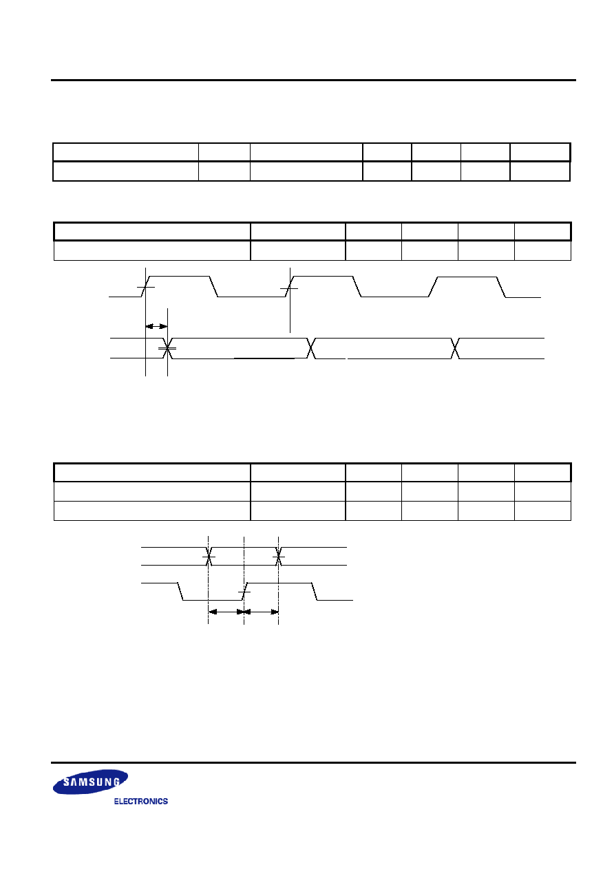
AC Characteristics
(V
DD
= 2.55V to 3.05V, Ta = -20 to + 60
∞
C)
(V
DDH
= 2.8V ± 0.25, T
a
= 0 to + 70 ∞C)
Setup and Hold Time
(V
DDL
= 1.8V ± 0.15, T
a
= 0 to + 70 ∞C, C
L
= 0.011pF)
Characteristic
Symbol
Condition
Min
Typ
Max
Unit
Main input clock frequency
f
MCLK
Duty = 50%
5
24.54
30
MHz
Characteristic
Symbol
Min
Typ
Max
Unit
Output Data Delay Time, Data [0:7]
T
DLY
0.5 - 3 ns
Characteristic
Symbol
Min
Typ
Max
Unit
Output Data Setup Time, Data [0:7]
T
SU
0.217 - - ns
Output Data Hold Time, Data [0:7]
T
HD
0.217
- - ns
VCK
YC9~0
Tdly
Data [0:7]
PCLK
DATA[0:7]
CLK
Tsu
Thd
50%
50%
50%
PRELIMINARY
SX5433M14X-X0B0
1/4" VGA CIS CAMERA MODULE
10
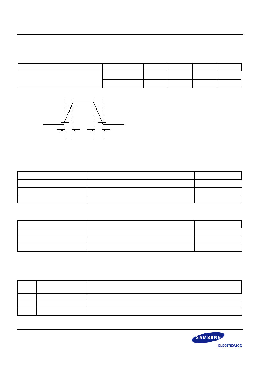
Rise and Fall Transition Time
(V
DDL
= 1.8V ± 0.15, T
a
= 0 to + 70 ∞C, C
L
= 0.011pF)
ESD Sensitivity
(CMOS Image Sensor IC)
Item Condition
Result
Human Body Model (HBM)
C = 100 pF, R = 1.5K
±
1500V
Machine Model (MM)
C = 200 pF, R = 0
±
200V
Charged Device Model (CDM)
±
800V
(Image Signal Processor IC)
Item Condition
Result
Human Body Model (HBM)
C = 100 pF, R = 1.5K
±
2000V
Machine Model (MM)
C = 200 pF, R = 0
±
200V
Charged Device Model (CDM)
±
500V
OUTPUT IMAGE MODE
No. Mode
Resolution
(H X V)
1 VGA
640X480
2 QVGA
320X240
3 QQVGA
160X120
Characteristic
Symbol
Min
Typ
Max
Unit
Output Data, Data [0:7]
T
R
- -
4.709
ns
T
F
-
-
4.338
ns
90%
90%
10%
10%
T
R
T
F
PRELIMINARY
1/4 INCH VGA CIS CAMERA MODULE
SX5433M14X-X0B0
11
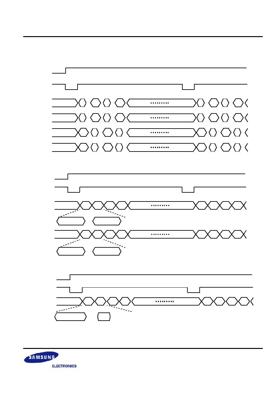
OUTPUT DATA FORMAT
YC
R
C
B
4:2:2 FORMAT
RGB565 FORMAT
SENSOR RAW IMAGE (BAYER MOSAIC PATTERN) FORMAT
HSYNC
VSYNC
DATA
(Mode1)
RG0 GB0 RG1 GB1
RG0 GB0 RG1 GB1
R0[4:0] / G0[5:3]
DATA
(Mode2)
GR0
BG0
GR1
BG1
GR0
BG0
GR1
BG1
G0[2:0] / B0[4:0]
B0[4:0] / G0[5:3]
G0[2:0] / R0[4:0]
HSYNC
VSYNC
DATA
D0H D0L D1H
D1L
D0H D0L D1H
D1L
6'b000000, D0[9:8]
D0[7:0]
HSYNC
VSYNC
DATA
(Mode1)
Y0
C
B
0
Y1
Y0
Y1
DATA
(Mode2)
Y0
Y1
Y0
Y1
DATA
(Mode3)
Y0
Y1
Y0
Y1
DATA
(Mode4)
Y0
Y1
Y0
Y1
C
R
0
C
B
0
C
R
0
C
B
0
C
B
0
C
R
0
C
R
0
C
B
0
C
R
0
C
B
0
C
R
0
C
B
0
C
B
0
C
R
0
C
R
0
PRELIMINARY
SX5433M14X-X0B0
1/4" VGA CIS CAMERA MODULE
12
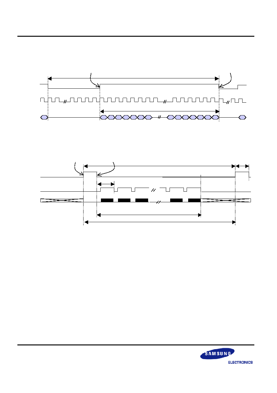
OUTPUT TIMING DIAGRAMS
HORIZONTAL TIMING
VGA OUTPUT TIMING
NOTES:
1. Falling and rising time of HSYNC and VSYNC can be controlled by register settings.
2. Each default value of rising and falling time control registers is described in the diagram above.
( 640 columns )
1 row
PCLK
HSYNC
Address : FAh[7:6]=0, F6h[7:0]=30
Address : FAh[5:4]=2, F7h[7:0]=B0
DATA [0:7]
( 640 columns )
1 row
PCLK
HSYNC
Address : FAh[7:6]=0, F6h[7:0]=30
Address : FAh[5:4]=2, F7h[7:0]=B0
DATA [0:7]
(480 rows )
(525 rows )
1 frame
1 row
2H
Address : FAh[3:2]=0, F8h[7:0]=03
Address : FAh[1:0]=0, F9h[7:0]=05
VSYNC
HSYNC
DATA [0:7]
(480 rows )
(525 rows )
1 frame
1 row
2H
Address : FAh[3:2]=0, F8h[7:0]=03
Address : FAh[1:0]=0, F9h[7:0]=05
VSYNC
HSYNC
DATA [0:7]
PRELIMINARY
1/4 INCH VGA CIS CAMERA MODULE
SX5433M14X-X0B0
13
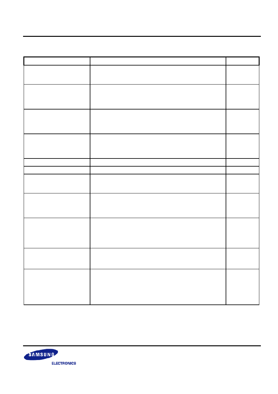
IMAGE PROCESSING FUNCTIONS
Function Description
Remarks
Defect detection and
correction
If enabled, the function detects the defective pixel by
comparing its level with horizontally neighboring pixels, and
replaces it with the average value of neighboring pixels.
De-mosaic
The sensor produces one color component from a pixel
according to Bayer color filter array. The de-mosaic function
performs color interpolation to produce all three-color
components at each pixel location.
Color correction
The spectral response of image sensor is different from that
of human eye. To match the spectral response, the sensor
output components are pivoted by user programmable 3X3
matrix production.
Gamma correction
Gamma correction translating the linear response of the
sensor into the non-linear characteristics of the display. Non-
linear conversion requires a piecewise linear approximation
method based on user programmable lookup table.
Horizontal mirror
The output image can be mirrored in horizontal direction.
Vertical mirror
The output image can be mirrored in vertical direction.
Edge enhancement
Enhancing the edge component provides a clear output
image. The edge enhancement function is performed through
horizontal and vertical edge detecting and enhancing.
Auto exposure
According to the incident light level, the auto exposure
function controls the sensor gain and effective integration time
to maintain the proper output level. Setting the control registers
can change the sensing area used in the AE algorithm.
Auto white balance
The auto white balance function adjusts the gain of the
sensor's red and blue channels relative to the green channel,
and compensates the spectral unbalancing of the light source.
Setting the control registers can change the sensing area used
in the AWB algorithm.
Output format conversion
4 types of output format are available.
(CCIR656 format, CCIR601 format, RGB format and sensor
raw image output format)
Sub-sampling Control
The user can read out the pixel data in sub-sampling rate in
both horizontal and vertical direction. Sub-sampling can be
done in two rates: full and 1/2. The user controls the sub-
sampling using the Sub-sampling Control Registers, subsr and
subsc. The sub-sampling is performed only in the Bayer
space.
PRELIMINARY
SX5433M14X-X0B0
1/4" VGA CIS CAMERA MODULE
14
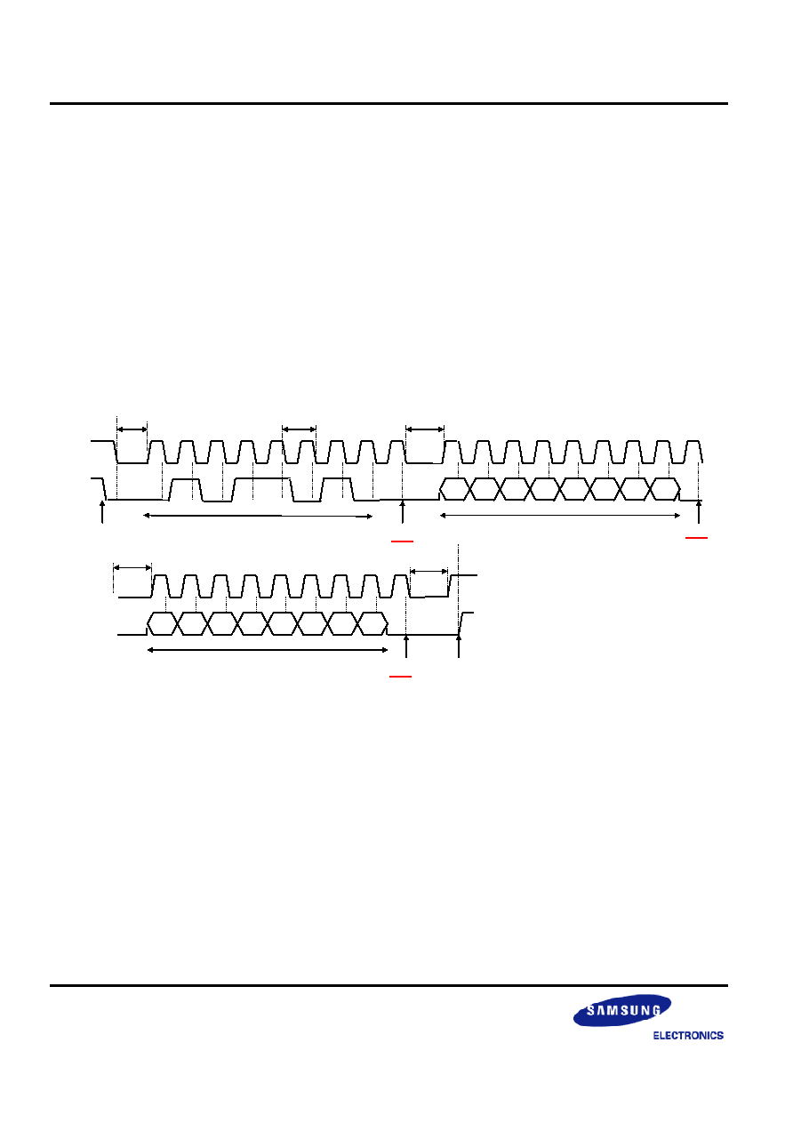
I
2
C SERIAL INTERFACE
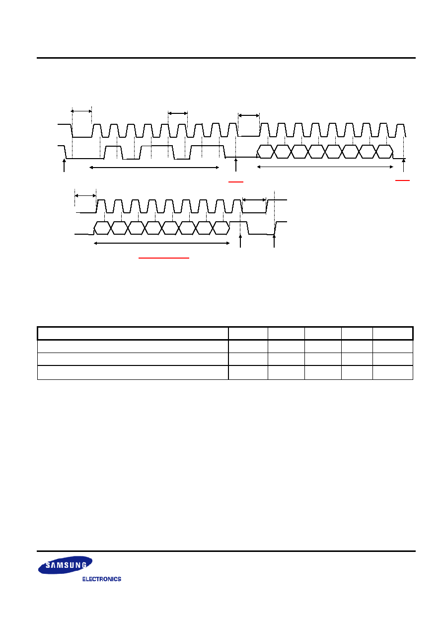
The I
2
C contains a serial two-wire half duplex interface that features bi-directional operation, master or slave
mode. The general SDA and SCL are the bi-directional data and clock pins, respectively. These pins are open-
drain type ports and will require a pull-up resistor to VDD. The image sensor operates in salve mode only and the
SCL is input only. The I
2
C bus interface is composed of following parts: START signal, 7-bit slave device address
(0101101Xb) transmission followed by a read/write bit, an acknowledgement signal from the slave, 8-bit data
transfer followed by an acknowledgement signal and STOP signal. The SDA bus line may only be changed while
SCL is low. The data on the SDA bus line is valid on the high-to-low transition of SCL.
I
2
C Bus Write Cycle
SDA
Start
D7
D6
D5
SCL
"0" "1" "0" "1" "1" "0" "1"
I
2
C Bus Address
I2C Register Address
Write
Ack
Ack
SDA
SCL
D7
Data to Write
Stop
Ack
D4
D5 D2 D1 D0
"0"
T1
T1
T1
T1
T2
D6
D1
D2
D3
D4
D5 D0
PRELIMINARY
1/4 INCH VGA CIS CAMERA MODULE
SX5433M14X-X0B0
15
Main Clock - 13.5MHz
Characteristic
Symbol
Min
Typ
Max
Unit
Low period of SCL clock
T1
13.5
15
-
µsec
Clock period
T2
13.5
15
-
µsec
Bus free time between a STOP and START condition
T
BUF
100 -
µsec
ACK
I
2
C Bus Read Cycle
STOP
D7
D6
D5
I2C Register Address
ACK
D4 D5 D2 D1
D0
D7 D6 D5
Data to be Read
Read
D4
D3
D2
D1
D0
SDA
START
SCL
"0" "1" "0"
"1" "1" "0"
"1"
I
2
C Bus Address
"1"
ACK
SDA
SCL
T1
T1
T1
T1
T2
NOTES:
1. The basic frequency of main clock is 13.5MHz for all the followed comments.
2. If you don't have ACK signal on the way of communications through I
2
C, it means that I
2
C error is generated.
3. If you have any I
2
C error, try again after 2VSYNC (The I
2
C error is reset every 2VSYNC automatically).
4. If any error is not generated till one command is completed, you can transfer another after 4msec
5. The time value of T1, T2, T3, and T
BUF
is proportional to the change of MCLK.
6.
I
2
C Bus read format is different from I
2
C standard format.
PRELIMINARY
SX5433M14X-X0B0
1/4" VGA CIS CAMERA MODULE
16
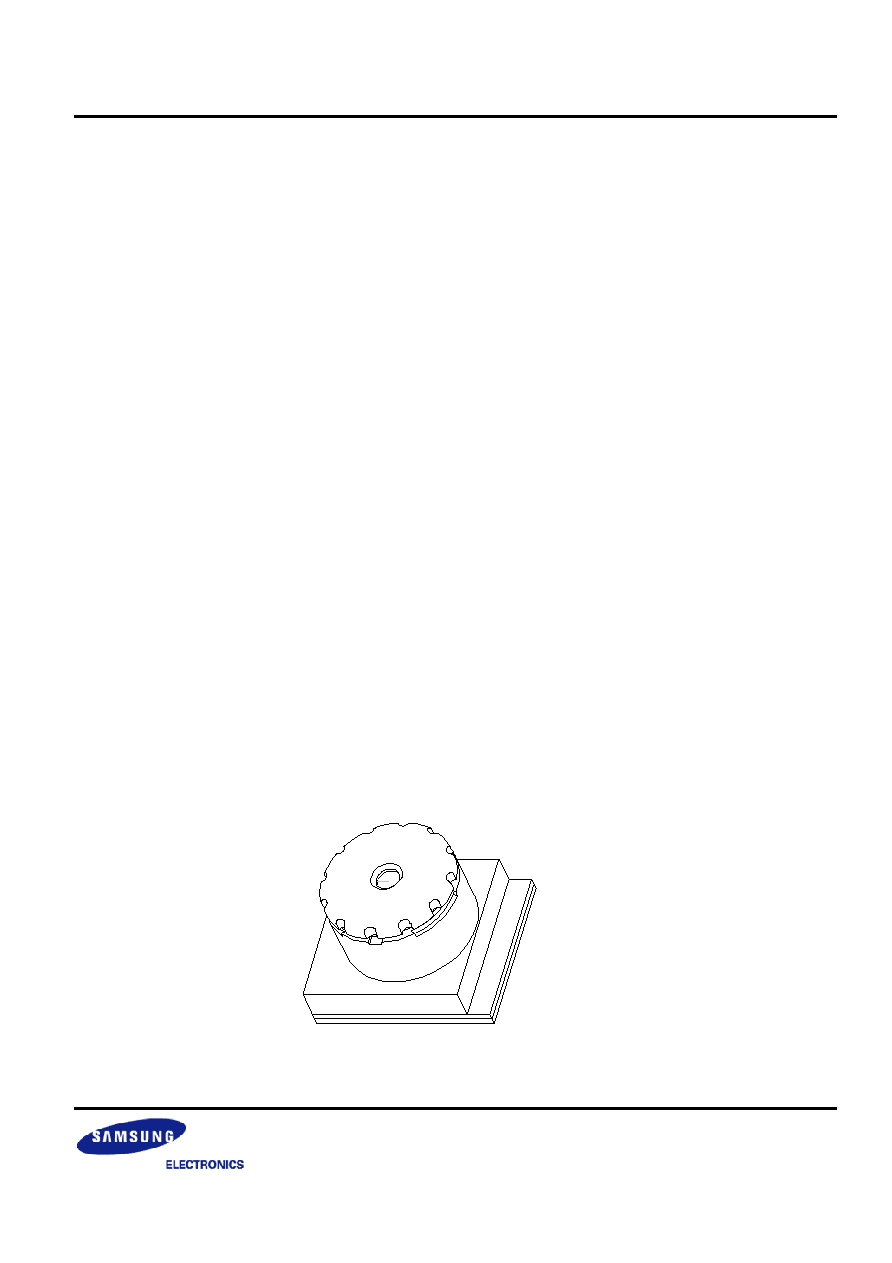
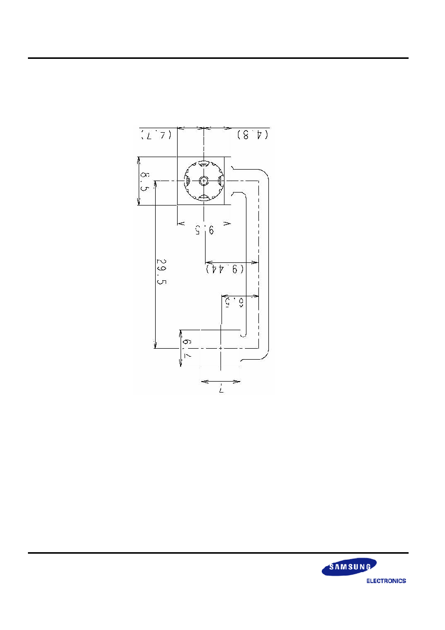
MECHANICAL DIMENSION (UNIT = MM)

PRELIMINARY
1/4 INCH VGA CIS CAMERA MODULE
SX5433M14X-X0B0
17
©2003 Samsung Electronics
All right reserved. No part of this publication may be reproduced, stored in a
retrieval system, or transmitted in any form or by any means, electric or
mechanical, by photocopying, recording, or otherwise, without the prior written
consent of Samsung Electronics.
Samsung Electronics Co., Ltd.
San #24 Nongseo-Ri, Giheung-Eup
Yongin-City, Gyeonggi-Do, Korea
C.P.O. Box #37, Suwon 449-900
Homepage:
http://www.samsungsemi.com/