
S3C2501X
32-BIT RISC
MICROPROCESSOR
USER'S MANUAL
Revision 1

Important Notice
The information in this publication has been carefully
checked and is believed to be entirely accurate at the
time of publication. Samsung assumes no
responsibility, however, for possible errors or
omissions, or for any consequences resulting from the
use of the information contained herein.
Samsung reserves the right to make changes in its
products or product specifications with the intent to
improve function or design at any time and without
notice and is not required to update this
documentation to reflect such changes.
This publication does not convey to a purchaser of
semiconductor devices described herein any license
under the patent rights of Samsung or others.
Samsung makes no warranty, representation, or
guarantee regarding the suitability of its products for
any particular purpose, nor does Samsung assume
any liability arising out of the application or use of any
product or circuit and specifically disclaims any and
all liability, including without limitation any
consequential or incidental damages.
"Typical" parameters can and do vary in different
applications. All operating parameters, including
"Typicals" must be validated for each customer
application by the customer's technical experts.
Samsung products are not designed, intended, or
authorized for use as components in systems
intended for surgical implant into the body, for other
applications intended to support or sustain life, or for
any other application in which the failure of the
Samsung product could create a situation where
personal injury or death may occur.
Should the Buyer purchase or use a Samsung product
for any such unintended or unauthorized application,
the Buyer shall indemnify and hold Samsung and its
officers, employees, subsidiaries, affiliates, and
distributors harmless against all claims, costs,
damages, expenses, and reasonable attorney fees
arising out of, either directly or indirectly, any claim of
personal injury or death that may be associated with
such unintended or unauthorized use, even if such
claim alleges that Samsung was negligent regarding
the design or manufacture of said product.
S3C2501X RISC Microprocessor
User's Manual, Revision 1
Publication Number: 21-S3-C2501X-122002
© 2002 Samsung Electronics
All rights reserved. No part of this publication may be reproduced, stored in a retrieval system, or transmitted in
any form or by any means, electric or mechanical, by photocopying, recording, or otherwise, without the prior
written consent of Samsung Electronics.
Samsung Electronics' Microprocessor business has been awarded full ISO-14001
certification (BSI Certificate No. FM24653). All semiconductor products are designed
and manufactured in accordance with the highest quality standards and objectives.
Samsung Electronics Co., Ltd.
San #24 Nongseo-Ri, Kiheung-Eup
Yongin-City, Kyunggi-Do, Korea
C.P.O. Box #37, Suwon 449-900
TEL: (82)-(31)-209-2831
FAX: (82)-(31)-209-8309
Home-Page URL: http://www.samsungsemi.com
Printed in the Republic of Korea

S3C2501X
iii
Table of Contents
Chapter 1
Product Overview
1.1 Overview ...........................................................................................................................................1-1
1.2 Features ............................................................................................................................................1-2
1.3 Block Diagram ...................................................................................................................................1-4
1.4 Package Diagram ..............................................................................................................................1-5
1.5 Pin Assignment..................................................................................................................................1-6
1.6 Signal Description ..............................................................................................................................1-12
1.7 Pad Type ...........................................................................................................................................1-26
1.8 Special Registers ...............................................................................................................................1-27
Chapter 2
Programmer's Model
2.1 Overview ...........................................................................................................................................2-1
2.2 Switching State ..................................................................................................................................2-1
2.2.1 Entering THUMB State ...........................................................................................................2-1
2.2.2 Entering ARM State ................................................................................................................2-1
2.3 Memory Formats................................................................................................................................2-2
2.3.1 Big-Endian Format..................................................................................................................2-2
2.3.2 Little-Endian Format ...............................................................................................................2-2
2.4 Instruction Length ..............................................................................................................................2-3
2.5 Data Types ........................................................................................................................................2-3
2.6 Operating Modes ...............................................................................................................................2-3
2.7 Registers ...........................................................................................................................................2-4
2.7.3 The Relationship Between ARM and THUMB State Registers.................................................2-7
2.7.4 Accessing Hi-Registers in THUMB State.................................................................................2-8
2.8 The Program Status Registers ...........................................................................................................2-8
2.8.1 The Condition Code Flags ......................................................................................................2-9
2.8.2 The Control Bits......................................................................................................................2-9
2.9 Exceptions .........................................................................................................................................2-11
2.9.1 Action on Entering an Exception .............................................................................................2-11
2.9.2 Action on Leaving an Exception..............................................................................................2-11
2.9.3 Exception Entry/Exit Summary ...............................................................................................2-12
2.9.4 FIQ .........................................................................................................................................2-12
2.9.5 IRQ.........................................................................................................................................2-13
2.9.6 Abort ......................................................................................................................................2-13
2.9.7 Software Interrupt ...................................................................................................................2-14
2.9.8 Undefined Instruction..............................................................................................................2-14
2.10 Exception Vectors ............................................................................................................................2-14
2.10.1 Exception Priorities...............................................................................................................2-15
2.10.2 Not All Exceptions Can Occur at Once: ................................................................................2-15
2.11 Interrupt Latencies ...........................................................................................................................2-16
2.12 Reset ...............................................................................................................................................2-16
2.13 Introduction for ARM940T ................................................................................................................2-17
2.14 ARM940T Block Diagram.................................................................................................................2-18
2.15 About The ARM940T Programmer's Model ......................................................................................2-19
2.15.1 Data Abort Model..................................................................................................................2-20
2.15.2 Instruction Set Extension Spaces..........................................................................................2-20
2.16 ARM940T CP15 Registers ...............................................................................................................2-21
2.16.1 CP15 Register Map Summary ..............................................................................................2-21

iv
S3C2501X
Table of Contents
(Continued)
Chapter 3
Instruction Set
3.1 Instruction Set Summay .................................................................................................................... 3-1
3.1.1 Format Summary................................................................................................................... 3-1
3.1.2 Instruction Summary.............................................................................................................. 3-2
3.2 The Condition Field........................................................................................................................... 3-4
3.3 Branch and Exchange (BX) ............................................................................................................... 3-5
3.3.1 Instruction Cycle Times.......................................................................................................... 3-5
3.3.2 Assembler Syntax.................................................................................................................. 3-5
3.3.3 Using R15 as an Operand...................................................................................................... 3-5
3.4 Branch and Branch with Link (B, BL) ................................................................................................. 3-7
3.4.1 The Link Bit ........................................................................................................................... 3-7
3.4.2 Instruction Cycle Times.......................................................................................................... 3-7
3.4.3 Assembler Syntax.................................................................................................................. 3-8
3.5 Data Processing................................................................................................................................ 3-9
3.5.1 CPSR Flags........................................................................................................................... 3-11
3.5.2 Shifts ..................................................................................................................................... 3-12
3.5.3 Immediate Operand Rotates .................................................................................................. 3-16
3.5.4 Writing to R15........................................................................................................................ 3-16
3.5.5 Using R15 as an Operand...................................................................................................... 3-16
3.5.6 Teq, Tst, Cmp and CMN Opcodes ......................................................................................... 3-16
3.5.7 Instruction Cycle Times.......................................................................................................... 3-17
3.6.8 Assembler Syntax.................................................................................................................. 3-17
3.6 PSR Transfer (MRS, MSR) ............................................................................................................... 3-19
3.6.1 Operand Restrictions ............................................................................................................. 3-19
3.6.2 Reserved Bits ........................................................................................................................ 3-21
3.6.3 Instruction Cycle Times.......................................................................................................... 3-21
3.6.4 Assembler Syntax.................................................................................................................. 3-22
3.7 Multiply and Multiply-Accumulate (MUL, MLA) .................................................................................. 3-23
3.7.1 CPSR Flags........................................................................................................................... 3-24
3.7.2 Instruction Cycle Times.......................................................................................................... 3-24
3.7.3 Assembler Syntax.................................................................................................................. 3-24
3.8 Multiply Long and Multiply-Accumulate Long (MULL, MLAL) ............................................................. 3-25
3.8.1 Operand Restrictions ............................................................................................................. 3-25
3.8.2 CPSR Flags........................................................................................................................... 3-26
3.8.3 Instruction Cycle Times.......................................................................................................... 3-26
3.8.4 Assembler Syntax.................................................................................................................. 3-27
3.9 Single Data Transfer (LDR, STR) ...................................................................................................... 3-28
3.9.1 Offsets and Auto-Indexing ..................................................................................................... 3-29
3.9.2 Shifted Register Offset........................................................................................................... 3-29
3.9.3 Bytes and Words ................................................................................................................... 3-29
3.9.4 Use of R15............................................................................................................................. 3-31
3.9.5 Restriction on the Use of Base Register ................................................................................. 3-31
3.9.6 Data Aborts............................................................................................................................ 3-31
3.9.7 Instruction Cycle Times.......................................................................................................... 3-31
3.9.8 Assembler Syntax.................................................................................................................. 3-32

S3C2501X
v
Table of Contents
(Continued)
Chapter 3
Instruction Set
(Continued)
3.10 Halfword and Signed Data Transfer (LDRH/STRH/LDRSB/LDRSH).................................................3-34
3.10.1 Offsets and Auto-Indexing ....................................................................................................3-35
3.10.2 Half-Word Load and Stores ..................................................................................................3-36
3.10.3 Signed Byte and Half-Word Loads ........................................................................................3-36
3.10.4 Endianness and Byte/Half-Word Selection............................................................................3-36
3.10.5 Use of R15 ...........................................................................................................................3-37
3.10.6 Data Aborts...........................................................................................................................3-37
3.10.7 Instruction Cycle Times ........................................................................................................3-37
3.10.8 Assembler Syntax.................................................................................................................3-38
3.11 Block Data Transfer (LDM, STM) .....................................................................................................3-40
3.11.1 The Register List...................................................................................................................3-40
3.11.2 Addressing Modes ................................................................................................................3-41
3.11.3 Address Alignment................................................................................................................3-41
3.11.4 Use of the S Bit ....................................................................................................................3-43
3.11.5 Use of R15 as the Base ........................................................................................................3-43
3.11.6 Inclusion of the Base in the Register List...............................................................................3-44
3.11.7 Data Aborts...........................................................................................................................3-44
3.11.8 Instruction Cycle Times ........................................................................................................3-44
3.11.9 Assembler Syntax.................................................................................................................3-45
3.12 Single Data Swap (SWP) .................................................................................................................3-47
3.12.1 Bytes and Words ..................................................................................................................3-47
3.12.2 Use of R15 ...........................................................................................................................3-47
3.12.3 Data Aborts...........................................................................................................................3-48
3.12.4 Instruction Cycle Times ........................................................................................................3-48
3.12.5 Assembler Syntax.................................................................................................................3-48
3.13 Software Interrupt (SWI) ..................................................................................................................3-49
3.13.1 Return from the Supervisor...................................................................................................3-49
3.13.2 Comment Field .....................................................................................................................3-49
3.13.3 Instruction Cycle Times ........................................................................................................3-49
3.13.4 Assembler Syntax.................................................................................................................3-50
3.14 Coprocessor Data Operations (CDP)................................................................................................3-51
3.14.1 Coprocessor Instructions.......................................................................................................3-51
3.14.2 The Coprocessor Fields ........................................................................................................3-51
3.14.3 Instruction Cycle Times ........................................................................................................3-52
3.14.4 Assembler Syntax.................................................................................................................3-52
3.15 Coprocessor Data Transfers (LDC, STC) .........................................................................................3-53
3.15.1 The Coprocessor Fields ........................................................................................................3-53
3.15.2 Addressing Modes ................................................................................................................3-54
3.15.3 Address Alignment................................................................................................................3-54
3.15.4 Use of R15 ...........................................................................................................................3-54
3.15.5 Data Aborts...........................................................................................................................3-54
3.15.6 Instruction Cycle Times ........................................................................................................3-54
3.15.7 Assembler Syntax.................................................................................................................3-55

vi
S3C2501X
Table of Contents
(Continued)
Chapter 3
Instruction Set
(Continued)
3.16 Coprocessor Register Transfers (MRC, MCR) ................................................................................. 3-56
3.16.1 The Coprocessor Fields ....................................................................................................... 3-56
3.16.2 Transfers to R15 .................................................................................................................. 3-57
3.16.3 Transfers from R15 .............................................................................................................. 3-57
3.16.4 Instruction Cycle Times........................................................................................................ 3-57
3.16.5 Assembler Syntax ................................................................................................................ 3-57
3.17 Undefined Instruction ...................................................................................................................... 3-58
3.17.1 Instruction Cycle Times........................................................................................................ 3-58
3.17.2 Assembler Syntax ................................................................................................................ 3-58
3.18 Instruction Set Examples................................................................................................................. 3-59
3.18.1 Using The Conditional Instructions ....................................................................................... 3-59
3.18.2 Pseudo-Random Binary Sequence Generator...................................................................... 3-61
3.18.3 Multiplication by Constant Using The Barrel Shifter.............................................................. 3-61
3.18.4 Loading a Word From an Unknown Alignment ..................................................................... 3-63
3.19 Thumb Instruction Set Format ......................................................................................................... 3-64
3.19.1 Format Summary................................................................................................................. 3-64
3.19.2 Opcode Summary................................................................................................................ 3-65
3.20 Format 1: Move Shifted Register..................................................................................................... 3-67
3.20.1 Operation............................................................................................................................. 3-67
3.20.2 Instruction Cycle Times........................................................................................................ 3-67
3.21 Format 2: Add/Subtract ................................................................................................................... 3-68
3.21.1 Operation............................................................................................................................. 3-68
3.21.2 Instruction Cycle Times........................................................................................................ 3-69
3.22 Format 3: Move/Compare/Add/Subtract Immediate......................................................................... 3-70
3.22.1 Operations ........................................................................................................................... 3-70
3.22.2 Instruction Cycle Times........................................................................................................ 3-70
3.23 Format 4: ALU Operations .............................................................................................................. 3-71
3.23.1 Operation............................................................................................................................. 3-71
3.23.2 Instruction Cycle Times........................................................................................................ 3-72
3.24 Format 5: Hi-Register Operations/Branch Exchange ....................................................................... 3-73
3.24.1 Operation............................................................................................................................. 3-73
3.24.2 Instruction Cycle Times........................................................................................................ 3-74
3.24.3 The Bx Instruction................................................................................................................ 3-74
3.24.4 Using R15 as an Operand .................................................................................................... 3-75
3.25 Format 6: PC-Relative Load............................................................................................................ 3-76
3.25.1 Operation............................................................................................................................. 3-76
3.25.2 Instruction Cycle Times........................................................................................................ 3-76
3.26 Format 7: Load/Store With Register Offset...................................................................................... 3-77
3.26.1 Operation............................................................................................................................. 3-77
3.26.2 Instruction Cycle Times........................................................................................................ 3-78
3.27 Format 8: Load/Store Sign-Extended Byte/Half-Word ..................................................................... 3-79
3.27.1 Operation............................................................................................................................. 3-79
3.27.2 Instruction Cycle Times........................................................................................................ 3-80

S3C2501X
vii
Table of Contents
(Continued)
Chapter 3
Instruction Set
(Continued)
3.28 Format 9: Load/Store with Immediate Offset ....................................................................................3-81
3.28.1 Operation..............................................................................................................................3-81
3.28.2 Instruction Cycle Times ........................................................................................................3-82
3.29 Format 10: Load/Store Half-Word ....................................................................................................3-83
3.29.1 Operation..............................................................................................................................3-83
3.29.2 Instruction Cycle Times ........................................................................................................3-83
3.30 Format 11: SP-Relative Load/Store .................................................................................................3-84
3.30.1 Operation..............................................................................................................................3-84
3.30.2 Instruction Cycle Times ........................................................................................................3-84
3.31 Format 12: Load Addres...................................................................................................................3-85
3.31.1 Operation..............................................................................................................................3-85
3.31.2 Instruction Cycle Times ........................................................................................................3-86
3.32 Format 13: Add Offset to Stack Pointer............................................................................................3-87
3.32.1 Operation..............................................................................................................................3-87
3.32.2 Instruction Cycle Times ........................................................................................................3-87
3.33 Format 14: Push/Pop Registers........................................................................................................3-88
3.33.1 Operation..............................................................................................................................3-88
3.33.2 Instruction Cycle Times ........................................................................................................3-89
3.34 Format 15: Multiple Load/Store ........................................................................................................3-90
3.34.1 Operation..............................................................................................................................3-90
3.34.2 Instruction Cycle Times ........................................................................................................3-90
3.35 Format 16: Conditional Branch.........................................................................................................3-91
3.35.1 Operation..............................................................................................................................3-91
3.35.2 Instruction Cycle Times ........................................................................................................3-92
3.36 Format 17: Software Interrupt ..........................................................................................................3-93
3.36.1 Operation..............................................................................................................................3-93
3.36.2 Instruction Cycle Times ........................................................................................................3-93
3.37 Format 18: Unconditional Branch .....................................................................................................3-94
3.37.1 Operation..............................................................................................................................3-94
3.38 Format 19: Long Branch With Link...................................................................................................3-95
3.38.1 Operation..............................................................................................................................3-95
3.38.2 Instruction Cycle Times ........................................................................................................3-96
3.39 Instruction Set Examples .................................................................................................................3-97
3.39.1 Multiplication by a Constant Using Shifts and Adds...............................................................3-97
3.39.2 General Purpose Signed Divide ............................................................................................3-98
3.39.3 Division by a Constant ..........................................................................................................3-100

viii
S3C2501X
Table of Contents
(Continued)
Chapter 4
System Configuration
4.1 Overview .......................................................................................................................................... 4-1
4.2 Features............................................................................................................................................ 4-1
4.3 Address Map..................................................................................................................................... 4-2
4.4 Remap of Memory Space ................................................................................................................. 4-3
4.5 External Address Translation ............................................................................................................ 4-3
4.6 Arbitration Scheme ........................................................................................................................... 4-4
4.6.1 Problem Solvings with Programmable Round-Robin .............................................................. 4-7
4.7 Clock Configuration........................................................................................................................... 4-9
4.8 System Configuration Special Registers............................................................................................ 4-15
4.8.1 System Configuration Register............................................................................................... 4-16
4.8.2 Product Code and Revision Number Register ........................................................................ 4-18
4.8.3 Clock Control Register ........................................................................................................... 4-19
4.8.4 Peripheral Clock Disable Register.......................................................................................... 4-20
4.8.5 Clock Status Register ............................................................................................................ 4-21
4.8.6 AHB Bus Master Priority Register .......................................................................................... 4-21
4.8.7 Core PLL Control Register ..................................................................................................... 4-22
4.8.8 System Bus PLL Control Register .......................................................................................... 4-23
4.8.9 PHY PLL Control Register ..................................................................................................... 4-24
Chapter 5
Memory Controller
5.1 Overview .......................................................................................................................................... 5-1
5.2 Features............................................................................................................................................ 5-2
5.3 Memory Map..................................................................................................................................... 5-3
5.4 Bus Interface Signals ........................................................................................................................ 5-5
5.5 Endian Modes ................................................................................................................................... 5-7
5.6 Ext I/O Bank Controller ..................................................................................................................... 5-13
5.6.1 Features ................................................................................................................................ 5-13
5.6.2 External Device Connection................................................................................................... 5-14
5.6.3 Ext. I/O Bank Controller Special Register............................................................................... 5-21
5.6.4 Timing Diagram ..................................................................................................................... 5-29
5.7 SDRAM Controller ............................................................................................................................ 5-38
5.7.1 Features ................................................................................................................................ 5-38
5.7.2 SDRAM Size and Configuration ............................................................................................. 5-39
5.7.3 Address Mapping ................................................................................................................... 5-42
5.7.4 SDRAM Commands............................................................................................................... 5-44
5.7.5 External Data Bus Width........................................................................................................ 5-45
5.7.6 Merging Write Buffer ............................................................................................................. 5-45
5.7.7 Self Refresh........................................................................................................................... 5-45
5.7.8 Basic Operation ..................................................................................................................... 5-46
5.7.9 SDRAM Special Registers ..................................................................................................... 5-47
5.7.10 SDRAM Controller Timing.................................................................................................... 5-54

S3C2501X
ix
Table of Contents
(Continued)
Chapter 6
I
2
C Bus Controller
6.1 Overview ...........................................................................................................................................6-1
6.2 Features ............................................................................................................................................6-1
6.3 Functional Description .......................................................................................................................6-2
6.4 I
2
C Concepts .....................................................................................................................................6-3
6.4.1 Basic Operation ......................................................................................................................6-3
6.4.2 General Characteristics ..........................................................................................................6-4
6.4.3 Bit Transfers ...........................................................................................................................6-4
6.4.4 Data Validity ...........................................................................................................................6-5
6.4.5 Start and Stop Conditions .......................................................................................................6-5
6.4.6 Data Transfer Operations .......................................................................................................6-6
6.5 I
2
C Special Registers .........................................................................................................................6-8
6.5.1 Control Status Register...........................................................................................................6-8
6.5.2 Shift Buffer Register ...............................................................................................................6-10
6.5.3 Prescaler Register ..................................................................................................................6-10
6.5.4 Prescaler Counter Register.....................................................................................................6-11
6.5.5 Interrupt Pending Register ......................................................................................................6-11
Chapter 7
Ethernet Controller
7.1 Overview ...........................................................................................................................................7-1
7.2 Features ............................................................................................................................................7-2
7.3 MAC Function Blocks.........................................................................................................................7-3
7.3.1 Media Independent Interface (MII) ..........................................................................................7-3
7.3.2 Physical Layer Entity (PHY)....................................................................................................7-4
7.3.3 Buffered Dma Interface (BDI) .................................................................................................7-4
7.3.4 The MAC Transmitter Block....................................................................................................7-4
7.3.5 The MAC Receiver Block........................................................................................................7-6
7.3.6 Flow Control Block..................................................................................................................7-7
7.3.7 Buffered DMA (BDMA) Overview ...........................................................................................7-7
7.4 Ethernet Controller Special Registers.................................................................................................7-13
7.4.1 BDMA Relative Special Register ............................................................................................7-15
7.4.2 MAC Relative Special Register...............................................................................................7-24
7.5 Ethernet Operations...........................................................................................................................7-37
7.5.1 MAC Frame Format................................................................................................................7-37
7.5.2 The MII Station Manager ........................................................................................................7-45
7.5.3 Full-Duplex Pause Operations ................................................................................................7-46
7.5.4 Error Signalling.......................................................................................................................7-48
7.5.5 Timing Parameters for MII Transactions .................................................................................7-50

x
S3C2501X
Table of Contents
(Continued)
Chapter 8
DES/3DES
8.1 Overview .......................................................................................................................................... 8-1
8.2 Feature ............................................................................................................................................. 8-1
8.3 DES/3DES Special Registers............................................................................................................ 8-3
8.3.1 DES/3DES Control Register................................................................................................... 8-4
8.3.2 DES/3DES Status Register .................................................................................................... 8-5
8.3.3 DES/3DES Interrupt Enable Register ..................................................................................... 8-6
8.3.4 DES/3DES Run Enable Register............................................................................................ 8-6
8.3.5 DES/3DES Key1 Left/Right Side Register.............................................................................. 8-6
8.3.6 DES/3DES Key 2 Left/Right Side Register............................................................................. 8-7
8.3.7 DES/3DES Key 3 Left Side Register ...................................................................................... 8-7
8.3.8 DES/3DES IV Left/Right Side Register .................................................................................. 8-7
8.3.9 DES/3DES Input/Output Data FIFO Register ......................................................................... 8-8
8.4 DES/3DES Operation........................................................................................................................ 8-9
8.5 Performance Calculation Guide ........................................................................................................ 8-10
Chapter 9
GDMA Controller
9.1 Overview .......................................................................................................................................... 9-1
9.2 Feature ............................................................................................................................................. 9-1
9.3 GDMA Special Registers................................................................................................................... 9-3
9.3.1 GDMA Programmable Priority Registers ................................................................................ 9-4
9.3.2 GDMA Control Registers........................................................................................................ 9-9
9.3.3 GDMA Source/Destination Address Registers........................................................................ 9-12
9.3.4 GDMA Transfer Count Registers............................................................................................ 9-13
9.3.5 GDMA Run Enable Registers................................................................................................. 9-14
9.3.6 GDMA Interrupt Pending Register.......................................................................................... 9-15
9.4 GDMA Mode Operation..................................................................................................................... 9-16
9.4.1 Software Mode....................................................................................................................... 9-16
9.4.2 External GDMA Request Mode .............................................................................................. 9-16
9.4.3 HUART Mode ........................................................................................................................ 9-16
9.4.4 DES Mode ............................................................................................................................. 9-17
9.5 GDMA Function Description .............................................................................................................. 9-17
9.5.1 GDMA Transfers.................................................................................................................... 9-17
9.5.2 Starting/Ending GDMA Transfers ........................................................................................... 9-17
9.5.3 Data Transfer Modes ............................................................................................................. 9-18
9.6 GDMA Transfer Timing Data............................................................................................................. 9-19
9.6.1 Single and One Data Burst Mode .......................................................................................... 9-20
9.6.2 Single and Four Data Burst Mode .......................................................................................... 9-21
9.6.3 Block and One Data Burst Mode ............................................................................................ 9-22
9.6.4 Block and Four Data Burst ..................................................................................................... 9-23

S3C2501X
xi
Table of Contents
(Continued)
Chapter 10 Serial I/O (Console UART)
10.1 Overview .........................................................................................................................................10-1
10.2 Features ..........................................................................................................................................10-1
10.3 Console UART Special Registers.....................................................................................................10-3
10.3.1 Console UART Control Registers..........................................................................................10-4
10.3.2 Console UART Status Registers ...........................................................................................10-8
10.3.3 Console UART Interrupt Enable Register ..............................................................................10-11
10.3.4 UART Transmit Data Register ..............................................................................................10-13
10.3.5 UART Receive Data Register ...............................................................................................10-14
10.3.6 UART Baud Rate Divisor Register ........................................................................................10-15
10.3.7 Console UART Baud Rate Examples....................................................................................10-16
10.3.8 UART Control Character Register 1 and 2 ............................................................................10-17
Chapter 11Serial I/O (High-Speed UART)
11.1 Overview .........................................................................................................................................11-1
11.2 Features ..........................................................................................................................................11-1
11.3 High-Speed UART Special Registers ...............................................................................................11-3
11.3.1 High-Speed UART Control Registers ....................................................................................11-4
11.3.2 High-Speed UART Status Registers......................................................................................11-9
11.3.3 High-Speed UART Interrupt Enable Register ........................................................................11-14
11.3.4 High-Speed UART Transmit Buffer Register .........................................................................11-16
11.3.5 High-Speed UART Receive Buffer Register ..........................................................................11-17
11.3.6 High-Speed UART Baud Rate Divisor Register .....................................................................11-18
11.3.7 High-Speed UART Baud Rate Examples ..............................................................................11-19
11.3.8 High-Speed UART Control Character 1 Register...................................................................11-20
11.3.9 High-Speed UART Control Character 2 Register...................................................................11-21
11.3.10 High-Speed UART Autoband Boundary Register.................................................................11-22
11.3.11 High-Speed UART Autobaud Table Regsiter.......................................................................11-23
11.4 High-Speed UART Operation ...........................................................................................................11-24
11.4.1 FIFO Operation ....................................................................................................................11-24
11.4.2 Hardware Flow Control .........................................................................................................11-24
11.4.3 Software Flow Control...........................................................................................................11-26
11.4.4 Auto Baud Rate Detection.....................................................................................................11-26
Chapter 12I/O Ports
12.1 Overview .........................................................................................................................................12-1
12.2 Features ..........................................................................................................................................12-1
12.3 I/O Port Special Register..................................................................................................................12-2
12.3.1 I/O Port Mode Select Register ..............................................................................................12-2
12.3.2 I/O Port Function Control Register ........................................................................................12-4
12.3.3 I/O Port Control Register for GDMA ......................................................................................12-7
12.3.4 I/O Port Control Register for External Interrupt .....................................................................12-8
12.3.5 I/O Port External Interrupt Clear Register..............................................................................12-10
12.3.6 I/O Port Data Register ..........................................................................................................12-11
12.3.7 I/O Port Drive Control Register .............................................................................................12-11

xii
S3C2501X
Table of Contents
(Concluded)
Chapter 13Interrupt Controller
13.1 Overview ........................................................................................................................................ 13-1
13.2 Features.......................................................................................................................................... 13-1
13.3 Interrupt Sources............................................................................................................................. 13-2
13.4 Interrupt Controller Special Registers .............................................................................................. 13-3
13.4.1 Interrupt Mode Registers...................................................................................................... 13-3
13.4.2 Interrupt Mask Registers ...................................................................................................... 13-5
12.4.3 Interrupt Priority Registers ................................................................................................... 13-8
13.4.4 Interrupt Offset Register....................................................................................................... 13-9
13.4.5 Interrupt by Priority Register ................................................................................................ 13-12
13.4.6 Interrupt Test Register ......................................................................................................... 13-12
Chapter 1432-bit Timers
14.1 Overview ........................................................................................................................................ 14-1
14.2 Feature ........................................................................................................................................... 14-1
14.3 Interval Mode Operation.................................................................................................................. 14-2
14.4 Toggle Mode Operation................................................................................................................... 14-2
14.5 Timer Operation Guidelines ............................................................................................................ 14-3
14.6 Timer Special Register.................................................................................................................... 14-4
14.6.1 Timer Mode Register ........................................................................................................... 14-4
14.6.2 Timer Data Registers ........................................................................................................... 14-6
14.6.3 Timer Count Registers ......................................................................................................... 14-7
14.6.4 Timer Interrupt Clear Registers ............................................................................................ 14-8
14.6.5 Watchdog Timer Register .................................................................................................... 14-9
Chapter 15Electrical Data
15.1 Overview ........................................................................................................................................ 15-1
15.2 Absolute Maximum Ratings............................................................................................................. 15-1
15.3 Recommended Operating Conditions .............................................................................................. 15-1
15.4 DC Electrical Specifications ............................................................................................................ 15-2
15.5 AC Electrical Characteristics ........................................................................................................... 15-4
Chapter 16Mechanical Data
16.1 Overview ........................................................................................................................................ 16-1

S3C2501X
xiii
List of Figures
Figure
Title
Page
Number
Number
1-1
S3C2501X Block Diagram ......................................................................................1-4
1-2
S3C2501X Pin Assignment Diagram ......................................................................1-5
2-1
Big-Endian Addresses of Bytes within Words..........................................................2-2
2-2
Little-Endian Addresses of Bytes Words .................................................................2-2
2-3
Register Organization in ARM State .......................................................................2-5
2-4
Register Organization in THUMB State ..................................................................2-6
2-5
Mapping of THUMB State Registers onto ARM State Registers..............................2-7
2-6
Program Status Register Format ............................................................................2-8
2-7
ARM940T Block Diagram .......................................................................................2-18
3-1
ARM Instruction Set Format ...................................................................................3-1
3-2
Branch and Exchange Instructions..........................................................................3-5
3-3
Branch Instructions.................................................................................................3-7
3-4
Data Processing Instructions ..................................................................................3-9
3-5
ARM Shift Operations.............................................................................................3-12
3-6
Logical Shift Left ....................................................................................................3-12
3-7
Logical Shift Right ..................................................................................................3-13
3-8
Arithmetic Shift Right .............................................................................................3-13
3-9
Rotate Right ...........................................................................................................3-14
3-10
Rotate Right Extended ...........................................................................................3-14
3-11
PSR Transfer .........................................................................................................3-20
3-12
Multiply Instructions................................................................................................3-23
3-13
Multiply Long Instructions .......................................................................................3-25
3-14
Single Data Transfer Instructions............................................................................3-28
3-15
Little-Endian Offset Addressing ..............................................................................3-30
3-16
Half-word and Signed Data Transfer with Register Offset .......................................3-34
3-17
Half-word and Signed Data Transfer with Immediate Offset and Auto-Indexing ......3-35
3-18
Block Data Transfer Instructions .............................................................................3-40
3-19
Post-Increment Addressing.....................................................................................3-41
3-20
Pre-Increment Addressing ......................................................................................3-42
3-21
Post-Decrement Addressing ...................................................................................3-42
3-22
Pre-Decrement Addressing.....................................................................................3-43
3-23
Swap Instruction .....................................................................................................3-47
3-24
Software Interrupt Instruction..................................................................................3-49
3-25
Coprocessor Data Operation Instruction .................................................................3-51
3-26
Coprocessor Data Transfer Instructions ..................................................................3-53
3-27
Coprocessor Register Transfer Instructions ............................................................3-56
3-28
Undefined Instruction..............................................................................................3-58
3-29
THUMB Instruction Set Formats .............................................................................3-64

xiv
S3C2501X
List of Figures
(Continued)
Figure
Title
Page
Number
Number
3-30
Format 1................................................................................................................ 3-67
3-31
Format 2................................................................................................................ 3-68
3-32
Format 3................................................................................................................ 3-70
3-33
Format 4................................................................................................................ 3-71
3-34
Format 5................................................................................................................ 3-73
3-35
Format 6................................................................................................................ 3-76
3-36
Format 7................................................................................................................ 3-77
3-37
Format 8................................................................................................................ 3-79
3-38
Format 9................................................................................................................ 3-81
3-39
Format 10.............................................................................................................. 3-83
3-40
Format 11.............................................................................................................. 3-84
3-41
Format 12.............................................................................................................. 3-85
3-42
Format 13.............................................................................................................. 3-87
3-43
Format 14.............................................................................................................. 3-88
3-44
Format 15.............................................................................................................. 3-90
3-45
Format 16.............................................................................................................. 3-91
3-46
Format 17.............................................................................................................. 3-93
3-47
Format 18.............................................................................................................. 3-94
3-48
Format 19.............................................................................................................. 3-95
4-1
S3C2501X Address map after resest ..................................................................... 4-2
4-2
External Address Bus Diagram .............................................................................. 4-4
4-3
Priority Groups of S3C2501X................................................................................. 4-5
4-4
AHB Programmable Priority Registers ................................................................... 4-6
4-5
Shows the Clock Generation Logic of the S3C2501X............................................. 4-14
4-6
Divided System Clock Timing Diagram.................................................................. 4-19
5-1
Memory Bank Address map................................................................................... 5-4
5-2
Memory Controller Bus Signals.............................................................................. 5-6
5-3
8-bit ROM, SRAM and Flash Basic Connection ..................................................... 5-14
5-4
8-bit ROM, SRAM and Flash Basic Connection (8-bit Memory x 2)........................ 5-15
5-5
16-bit SRAM Basic Connection.............................................................................. 5-16
5-6
16-bit ROM and Flash Basic Connection ............................................................... 5-17
5-7
16-bit ROM Basic Connection 2............................................................................. 5-18
5-8
16-bit SRAM Basic Connection 2 ........................................................................... 5-19
5-9
ROM & SRAM with Muxed Address & Data Bus Connection.................................. 5-20
5-10
BnCON.................................................................................................................. 5-22
5-11
Bank n Control (BnCON) Register Configuration.................................................... 5-24
5-12
Muxed Bus Control (MUXBCON) Register Configuration ....................................... 5-26
5-13
Wait Control (WAITCON) Register Configuration .................................................. 5-28

S3C2501X
xv
List of Figures
(Continued)
Figure
Title
Page
Number
Number
5-14
Read Timing Diagram 1 .........................................................................................5-29
5-15
Write Timing Diagram 1 .........................................................................................5-30
5-16
Read Timing Diagram 2 .........................................................................................5-31
5-17
Write Timing Diagram 2 .........................................................................................5-32
5-18
Read after Write at the Same Bank (COHDIS = 1) .................................................5-33
5-19
Read Timing Diagram (Muxed Bus)........................................................................5-34
5-20
Write Timing Diagram (Muxed Bus) .......................................................................5-35
5-21
Write Timing Diagram (nEWAIT)............................................................................5-36
5-22
Write Timing Diagram (nREADY) ...........................................................................5-37
5-23
SDRAM Configuration Register 0 ...........................................................................5-49
5-24
SDRAM Command Register ...................................................................................5-51
5-25
SDRAM Refresh Timer Register.............................................................................5-52
5-26
SDRAM Write Buffer Time-out Register .................................................................5-53
5-27
Single Read Operation (CAS Latency=2)................................................................5-54
5-28
Single Read Operation (CAS Latency=3)................................................................5-55
5-29
Single Write Operation ...........................................................................................5-56
5-30
Burst Read Operation (CAS Latency = 2) ...............................................................5-57
5-31
Burst Read Operation (CAS Latency = 3) ...............................................................5-58
5-32
Burst Write Operation.............................................................................................5-59
6-1
I
2
C Block Diagram..................................................................................................6-1
6-2
Master Transmitter and Slave Receiver..................................................................6-3
6-3
Master Receiver and Slave Transmitter..................................................................6-4
6-4
Start and Stop Conditions.......................................................................................6-5
6-5
Data Transfer Format .............................................................................................6-7
6-6
I
2
C Control Status Register.....................................................................................6-10
7-1
Ethernet Diagram ...................................................................................................7-1
7-2
Data Structure of Tx Buffer Descriptor....................................................................7-10
7-3
Data Structure of Rx Buffer Descriptor ...................................................................7-11
7-4
Data Structure of the Receive Frame .....................................................................7-12
7-5
Fields of an IEEE802.3/Ethernet Frame .................................................................7-38
7-6
CSMA/CD Transmit Operation ...............................................................................7-40
7-7
Timing for Transmission without Collision...............................................................7-41
7-8
Timing for Transmission with Collision in Preamble ................................................7-42
7-9
Receiving Frame without Error ...............................................................................7-43
7-10
Receiving Frame with Error ....................................................................................7-43
7-11
CSMA/CD Receive Operation ................................................................................7-44
7-12
MAC Control Frame Format ...................................................................................7-46
7-13
Timing Relationship of Transmission Signals at MII................................................7-50
7-14
Timing Relationship of Reception Signals at MII.....................................................7-50
7-15
MDIO Sourced by PHY...........................................................................................7-50
7-16
MDIO Sourced by STA ...........................................................................................7-50
8-1
DES/3DES Block Diagram .....................................................................................8-2

xvi
S3C2501X
List of Figures
(Continued)
Figure
Title
Page
Number
Number
9-1
GDMA Controller Block Diagram ........................................................................... 9-2
9-2
GDMA Programmable Priority Registers................................................................ 9-5
9-3
GDMA Control Register ......................................................................................... 9-11
9-4
GDMA Source/Destination Address Register ......................................................... 9-12
9-5
GDMA Transfer Count Register ............................................................................. 9-13
9-6
GDMA Run Enable Register .................................................................................. 9-14
9-7
GDMA Interrupt Pending Register.......................................................................... 9-15
9-8
External GDMA Requests (Single Mode) ............................................................... 9-18
9-9
External GDMA Requests (Block Mode) ................................................................ 9-18
9-10
External GDMA Requests Detailed Timing ............................................................ 9-19
9-11
Single and One Data Burst Mode Timing ............................................................... 9-20
9-12
Single and Four Data Burst Mode Timing .............................................................. 9-21
9-13
Block and One Data Burst Mode Timing ................................................................ 9-22
9-14
Block and Four Data Burst Timing ......................................................................... 9-23
10-1
Console UART Block Diagram............................................................................... 10-2
10-2
Console UART Control Register ............................................................................ 10-6
10-3
Console UART Control Register ............................................................................ 10-7
10-4
Console UART Status Register.............................................................................. 10-10
10-5
Console UART Interrupt Enable Register............................................................... 10-12
10-6
Console UART Transmit Data Register.................................................................. 10-13
10-7
Console UART Receive Data Register................................................................... 10-14
10-8
Console UART Baud Rate Divisor Register ........................................................... 10-15
10-9
Console UART Baud Rate Generator (BRG).......................................................... 10-16
10-10
Console UART Control Character 1 Register ......................................................... 10-17
10-11
Console UART Control Character 2 Register ......................................................... 10-17
10-12
Interrupt-Based Serial I/O Transmit and Receive Timing Diagram ......................... 10-18
10-13
Serial I/O Frame Timing Diagram (Normal Console UART) ................................... 10-19
10-14
Infra-Red Transmit Mode Frame Timing Diagram.................................................. 10-19
10-15
Infra-Red Receive Mode Frame Timing Diagram................................................... 10-20
11-1
High-Speed UART Block Diagram ......................................................................... 11-2
11-2
High-Speed UART Control Register....................................................................... 11-7
11-3
High-Speed UART Status Register ........................................................................ 11-12
11-4
High-Speed UART Interrupt Enable Register ......................................................... 11-15
11-5
High-Speed UART Transmit Buffer Register.......................................................... 11-16
11-6
High-Speed UART Receive Buffer Register........................................................... 11-17
11-7
High-Speed UART Baud Rate Divisor Register...................................................... 11-18
11-8
High-Speed UART Baud Rate Generator (BRG).................................................... 11-19
11-9
High-Speed UART Control Character 1 Register.................................................... 11-20
11-10
High-Speed UART Control Character 2 Register.................................................... 11-21

S3C2501X
xvii
List of Figures
(Concluded)
Figure
Title
Page
Number
Number
11-11
AutoBaud Boundary Register Range ......................................................................11-22
11-12
High-Speed UART AutoBaud Boundary Register....................................................11-22
11-13
Example of AutoBaud Table Register Setting .........................................................11-23
11-14
High-Speed UART AutoBaud Table Register..........................................................11-23
11-15
When CTS Signal Level is High During Transmit Operation ...................................11-25
11-16
When CTS Signal Level is Low During Transmit Operation ....................................11-25
11-17
Normal Received Rx Data ......................................................................................11-26
11-18
DCD Lost During Rx Data Receive .........................................................................11-26
11-19
Interrupt-Based Serial I/O Transmit and Receive Timing Diagram..........................11-27
11-20
DMA-Based Serial I/O Timing Diagram (Tx Only)...................................................11-28
11-21
DMA-Based Serial I/O Timing Diagram (Rx Only) ..................................................11-28
11-22
Serial I/O Frame Timing Diagram (Normal High-Speed UART) ..............................11-29
11-23
Infra-Red Transmit Mode Frame Timing Diagram...................................................11-29
11-24
Infra-Red Receive Mode Frame Timing Diagram ...................................................11-30
12-1
I/O Port Mode Registers 1/2 ...................................................................................12-3
12-2
I/O Function Control Register 1 ..............................................................................12-5
12-3
I/O Function Control Register 2 ..............................................................................12-6
12-4
I/O Port Control Register for GDMA........................................................................12-7
12-5
I/O Port Control Register for External Interrupt .......................................................12-9
12-6
I/O Port External Interrupt Clear Register ...............................................................12-10
13-1
Internal Interrupt Mode Register .............................................................................13-4
13-2
External Interrupt Mode Register ............................................................................13-5
13-3
Internal Interrupt Mask Register..............................................................................13-6
13-4
External Interrupt Mask Register ............................................................................13-7
13-5
Interrupt Priority Register........................................................................................13-8
14-1
Timer Output Signal Timing....................................................................................14-2
14-2
32-Bit Timer Block Diagram ...................................................................................14-3
14-3
Timer Mode Register ..............................................................................................14-5
14-4
Timer Data Registers..............................................................................................14-6
14-5
Timer Count Registers............................................................................................14-7
14-6
Timer Interrupt Clear Register ................................................................................14-8
14-7
Watchdog Timer Register.......................................................................................14-9
16-1
272-BGA-2727-AN Package Dimensions................................................................16-2


S3C2501X
xix
List of Tables
Table
Title
Page
Number
Number
1-1
S3C2501X Signal Descriptions ...............................................................................1-12
1-2
S3C2501X Pad Type and Feature ..........................................................................1-26
1-3
S3C2501X System Configuration ...........................................................................1-27
1-4
S3C2501X Memory Controller ................................................................................1-27
1-5
S3C2501X SDRAM Controller ................................................................................1-27
1-6
S3C2501X IIC Controller ........................................................................................1-28
1-7
S3C2501X Ethernet Controller 0.............................................................................1-28
1-8
S3C2501X Ethernet Controller 1.............................................................................1-29
1-9
S3C2501X DES Controller......................................................................................1-30
1-10
S3C2501X GDMA Controller ..................................................................................1-31
1-11
S3C2501X Console UART Controller......................................................................1-32
1-12
S3C2501X High speed UART Controller.................................................................1-32
1-13
S3C2501X I/O Port Controller.................................................................................1-33
1-14
S3C2501X Interrupt Controller................................................................................1-33
1-15
S3C2501X Timer Controller....................................................................................1-34
2-1
PSR Mode. Bit Values ............................................................................................2-10
2-2
Exception Entry/Exit ...............................................................................................2-12
2-3
Exception Vectors ..................................................................................................2-14
2-4
ARM9TDMI Implementation Option ........................................................................2-19
2-5
CP15 Register Map ................................................................................................2-21
2-6
ID Code Register....................................................................................................2-21
2-7
Cache Type Register Format..................................................................................2-22
2-8
CP15 Register 1 .....................................................................................................2-23
2-9
Clocking Modes......................................................................................................2-23
2-10
Cacheable Register Format ....................................................................................2-24
2-11
Write Buffer Control Register .................................................................................2-25
2-12
Protection Space Register Format ..........................................................................2-26
2-13
Permission Encoding..............................................................................................2-26
2-14
CP15 Data Protection Region Registers .................................................................2-27
2-15
CP15 Instruction Protection Region Registers ........................................................2-27
2-16
CP15 Protection Region Register Format ...............................................................2-28
2-17
Area Size Encoding ................................................................................................2-28
2-18
Cache Operations Writing to Register 7..................................................................2-29
2-19
CP15 Register 7 Index/Segment Data Format ........................................................2-30
2-20
CP15 Register 7 Prefetch Address Format .............................................................2-30
2-21
Lockdown Register Format .....................................................................................2-31
2-22
CP15 Register 15 ...................................................................................................2-32

xx
S3C2501X
List of Tables
(Continued)
Table
Title
Page
Number
Number
3-1
The ARM Instruction Set........................................................................................ 3-2
3-2
Condition Code Summary...................................................................................... 3-4
3-3
ARM Data Processing Instructions......................................................................... 3-11
3-4
Incremental Cycle Times ....................................................................................... 3-17
3-5
Assembler Syntax Descriptions ............................................................................. 3-27
3-6
Addressing Mode Names....................................................................................... 3-45
3-7
THUMB Instruction Set Opcodes ........................................................................... 3-65
3-8
Summary of Format 1 Instructions......................................................................... 3-67
3-9
Summary of Format 2 Instructions......................................................................... 3-68
3-10
Summary of Format 3 Instructions......................................................................... 3-70
3-11
Summary of Format 4 Instructions......................................................................... 3-71
3-12
Summary of Format 5 Instructions......................................................................... 3-74
3-13
Summary of PC-Relative Load Instruction ............................................................. 3-76
3-14
Summary of Format 7 Instructions......................................................................... 3-77
3-15
Summary of format 8 instructions .......................................................................... 3-79
3-16
Summary of Format 9 Instructions......................................................................... 3-81
3-17
Half-word Data Transfer Instructions...................................................................... 3-83
3-18
SP-Relative Load/Store Instructions ...................................................................... 3-84
3-19
Load Address ........................................................................................................ 3-85
3-20
The ADD SP Instruction......................................................................................... 3-87
3-21
PUSH and POP Instructions .................................................................................. 3-88
3-22
The Multiple Load/Store Instructions...................................................................... 3-90
3-23
The Conditional Branch Instructions ...................................................................... 3-91
3-24
The SWI Instruction............................................................................................... 3-92
3-25
Summary of Branch Instruction.............................................................................. 3-93
3-26
The BL Instruction ................................................................................................. 3-94
4-1
The Base Address of Remapped Memory.............................................................. 4-3
4-2
AHB Bus Priorities for Arbitration........................................................................... 4-4
4-3
Clock Frequencies for CLKMOD Pins, CPU_FREQ Pins, and BUS_FREQ Pins .... 4-9
4-4
P, M, S values of the S3C2501X PLL .................................................................... 4-13
4-5
System Configuration Registers............................................................................. 4-15

S3C2501X
xxi
List of Tables
(Continued)
Table
Title
Page
Number
Number
5-1
Base Address of Each Bank ...................................................................................5-3
5-2
Bus Interface Signals..............................................................................................5-5
5-3
External 32-bit Datawidth Store Operation with Big-Endian.....................................5-7
5-4
External 32-bit Datawidth Load Operation with Big-Endian .....................................5-7
5-5
External 16-bit Datawidth Store Operation with Big-Endian.....................................5-8
5-6
External 16-bit Datawidth Load Operation with Big-Endian .....................................5-8
5-7
External 8-bit Datawidth Store Operation with Big-Endian ......................................5-9
5-8
External 8-bit Datawidth Load Operation with Big-Endian .......................................5-9
5-9
External 32-bit Datawidth Store Operation with Little-Endian ..................................5-10
5-10
External 32-bit Datawidth Load Operation with Little-Endian...................................5-10
5-11
External 16-bit Datawidth Store Operation with Little-Endian ..................................5-11
5-12
External 16-bit Datawidth Load Operation with Little-Endian...................................5-11
5-13
External 8-bit Datawidth Store Operation with Little-Endian ....................................5-12
5-14
External 8-bit Datawidth Load Operation with Little-Endian.....................................5-12
5-15
Ext. I/O Bank Controller Special Registers .............................................................5-21
5-16
Bank n Control (BnCON) Register ..........................................................................5-23
5-17
Muxed Bus Control Register ...................................................................................5-25
5-18
WAIT Control Register ...........................................................................................5-27
5-19
Supported SDRAM Configuration of 32-bit External Bus.........................................5-40
5-20
Supported SDRAM Configuration of 16-bit External Bus.........................................5-41
5-21
SDRAM Address Mapping of 32-bit External Bus ...................................................5-42
5-22
SDRAM address mapping of 16-bit external bus.....................................................5-43
5-23
SDRAM commands ................................................................................................5-44
5-24
SDRAM Special Registers......................................................................................5-47
5-25
SDRAM Configuration Register ..............................................................................5-47
5-26
SDRAM Command Register ...................................................................................5-50
5-27
SDRAM Refresh Timer Register.............................................................................5-52
5-28
SDRAM Write Buffer Time-out Register .................................................................5-53
6-1
Control Status Register...........................................................................................6-8
6-2
IICCON Register Description ..................................................................................6-8
6-3
IICBUF Register .....................................................................................................6-10
6-4
IICPS Register .......................................................................................................6-10
6-5
IICCNT Register .....................................................................................................6-11
6-6
IICPND Register.....................................................................................................6-11

xxii
S3C2501X
List of Tables
(Continued)
Table
Title
Page
Number
Number
7-1
MAC Function Block Descriptions .......................................................................... 7-3
7-2
ETHERNET 0 Special Registers ............................................................................ 7-13
7-3
ETHERNET 1 Special Registers ............................................................................ 7-14
7-4
BDMATXCON Register.......................................................................................... 7-15
7-5
BDMA RXCON Register ........................................................................................ 7-16
7-6
BDMATXDPTR Register........................................................................................ 7-17
7-7
BDMARXDPTR Register ....................................................................................... 7-17
7-8
BTXBDCNT Register ............................................................................................. 7-18
7-9
BRXBDCNT Register............................................................................................. 7-18
7-10
BMTXINTEN Register............................................................................................ 7-19
7-11
BMTXSTAT Register ............................................................................................. 7-20
7-12
BMRXINTEN Register ........................................................................................... 7-21
7-13
BMRXSTAT Register............................................................................................. 7-22
7-14
BDMARXLEN Register .......................................................................................... 7-23
7-15
CFTXSTAT Register.............................................................................................. 7-24
7-16
MACCON Register ................................................................................................ 7-25
7-17
CAMCON Register ................................................................................................ 7-26
7-18
MACTXCON Register............................................................................................ 7-27
7-19
MACTXSTAT Register........................................................................................... 7-28
7-20
MACRXCON Register............................................................................................ 7-29
7-21
MACRXSTAT Register .......................................................................................... 7-30
7-22
STADATA Register................................................................................................ 7-31
7-23
STACON Register ................................................................................................. 7-32
7-24
CAMEN Register ................................................................................................... 7-33
7-25
MISSCNT Register ................................................................................................ 7-34
7-26
PZCNT Register .................................................................................................... 7-35
7-27
RMPZCNT Register............................................................................................... 7-35
7-28
CAM Register ........................................................................................................ 7-36
7-29
MAC Frame Format Description ............................................................................ 7-37
7-30
STA Frame Structure Description .......................................................................... 7-45

S3C2501X
xxiii
List of Tables
(Continued)
Table
Title
Page
Number
Number
8-1
DES/3DES Special Registers Overview .................................................................8-3
8-2
DES/3DES Control Register Description.................................................................8-4
8-3
DES/3DES Status Register Description ..................................................................8-5
8-4
DES/3DES Interrupt Enable Register Description ...................................................8-6
8-5
DES/3DES Run Enable Register Description..........................................................8-6
8-6
DES/3DES Key1 Left Side Register Description .....................................................8-6
8-7
DES/3DES Key 1 Right Side Register Description ..................................................8-6
8-8
DES/3DES Key 2 Left Side Register Description ....................................................8-7
8-9
DES/3DES Key 2 Right Side Register Description..................................................8-7
8-10
DES/3DES Key 3 Left Side Register Description ....................................................8-7
8-11
DES/3DES Key 3 Right Side Register Description ..................................................8-7
8-12
DES/3DES IV Left Side Register Description..........................................................8-7
8-13
DES/3DES IV Right Side Register Description .......................................................8-7
8-14
DES/3DES Input Data FIFO Description.................................................................8-8
8-15
DES/3DES Output Data FIFO Description ..............................................................8-8
9-1
GDMA Special Registers Overview ........................................................................9-3
9-2
GDMA Programmable Priority Registers ................................................................9-4
9-3
DCON0/1/2/3/4/5 Registers ....................................................................................9-9
9-4
GDMA Control Register Description .......................................................................9-9
9-5
DSAR0/1/2/3/4/5 and DDAR0/1/2/3/4/5 Registers...................................................9-12
9-6
DTCR0/1/2/3/4/5 Registers.....................................................................................9-13
9-7
DRER0/1/2/3/4/5 Registers.....................................................................................9-14
9-8
DIPR0/1/2/3 Registers ............................................................................................9-15

xxiv
S3C2501X
List of Tables
(Continued)
Table
Title
Page
Number
Number
10-1
Console UART Special Registers Overview........................................................... 10-3
10-2
CUCON Registers ................................................................................................. 10-4
10-3
Console UART Control Register Description .......................................................... 10-4
10-4
CUSTAT Registers ................................................................................................ 10-8
10-5
Console UART Status Register Description ........................................................... 10-8
10-6
CUINT Registers ................................................................................................... 10-11
10-7
Console UART Interrupt Enable Register Description ............................................ 10-11
10-8
CUTXBUF Registers.............................................................................................. 10-13
10-9
Console UART Transmit Register Description........................................................ 10-13
10-10
CURXBUF Registers ............................................................................................. 10-14
10-11
Console UART Receive Register Description ........................................................ 10-14
10-12
CUBRD Registers.................................................................................................. 10-15
10-13
Typical Baud Rates Examples of Console UART ................................................... 10-16
10-14
CUCHAR 1, 2 Registers ........................................................................................ 10-17
11-1
High-Speed UART Special Registers Overview ..................................................... 11-3
11-2
High-Speed UART Control Register...................................................................... 11-4
11-3
High-Speed UART Control Register Description .................................................... 11-4
11-4
High-Speed UART Status Register ........................................................................ 11-9
11-5
High-Speed UART Status Register Description...................................................... 11-9
11-6
High-Speed UART Interrupt Enable Register ......................................................... 11-14
11-7
High-Speed UART Interrupt Enable Register Description....................................... 11-14
11-8
High-Speed UART Transmit Register .................................................................... 11-16
11-9
High-Speed UART Transmit Register Description .................................................. 11-16
11-10
High-Speed UART Receive Register ..................................................................... 11-17
11-11
High-Speed UART Receive Register Description................................................... 11-17
11-12
High-Speed UART Transmit Register .................................................................... 11-18
11-13
Typical Baud Rates Examples of High-Speed UART ............................................. 11-19
11-14
High-Speed UART Control Charater 1 Register ..................................................... 11-20
11-15
High-Speed UART Control Character 2 Register.................................................... 11-21
11-16
High-Speed UART AutoBaud Boundary Register................................................... 11-22
11-17
High-Speed UART AutoBaud Table Register ......................................................... 11-23
12-1
I/O Port Special Registers ..................................................................................... 12-2
12-2
IOPMODE1/2 Registers......................................................................................... 12-2
12-3
IOPCON1/2 Register ............................................................................................. 12-4
12-4
IOPGDMA Register ............................................................................................... 12-7
12-5
IOPEXTINT Register ............................................................................................. 12-8
12-6
IOPEXTINTPND Register ...................................................................................... 12-10
12-7
IOPDATA1/2 Register............................................................................................ 12-11
12-8
IOPDRV1/2 Register.............................................................................................. 12-11

S3C2501X
xxv
List of Tables
(Concluded)
Table
Title
Page
Number
Number
13-1
S3C2501X Internal Interrupt Sources......................................................................13-2
13-2
S3C2501X External Interrupt Sources ....................................................................13-3
13-3
INTMOD, EXTMOD Register ..................................................................................13-3
13-4
INTMASK, EXTMASK Register ..............................................................................13-5
13-5
Interrupt Priority Register........................................................................................13-8
13-6
INTOFFSET_FIQ, INTOFFSET_IRQ Register .......................................................13-9
13-7
Index Value of Interrupt Sources ............................................................................13-10
13-8
IPRIORHI, IPRIORLO Register ..............................................................................13-12
13-9
INTTSTHI, INTTSTLO Register..............................................................................13-12
14-1
TMOD Register ......................................................................................................14-4
14-2
TDATA0 - TDATA5 Registers .................................................................................14-6
14-3
TCNT0 - TCNT5 Registers .....................................................................................14-7
14-4
Timer Interrupt Clear Registers...............................................................................14-8
14-5
WDT Register ........................................................................................................14-9
14-6
Watchdog Timer Timeout Value .............................................................................14-10
15-1
Absolute Maximum Ratings ....................................................................................15-1
15-2
Recommended Operating Conditions .....................................................................15-1
15-3
D.C Electric Characteristics ....................................................................................15-2
15-4
Operating Frequency..............................................................................................15-4
15-5
Clock AC timing specification- ................................................................................15-4
15-6
AC Electrical Characteristics for S3C2501X............................................................15-5

S3C2501X
PRODUCT OVERVIEW
1-1
1
PRODUCT OVERVIEW
1.1 OVERVIEW
Samsung's S3C2501X 16/32-bit RISC microcontroller is a cost-effective, high-performance microcontroller
solution for Ethernet-based systems, for example, SOHO router, internet gateway, WLAN AP, etc.
A variety of communication features are embedded into S3C2501X required in many communication areas,
including two Ethernet MACs, a high speed UART, and a console UART. A security feature is also supported by
DES/3DES accelerator.
This highly integrated microcontroller enables customers to save system costs and increase performance
over other 32-bit microcontroller.
The S3C2501X is built based on an outstanding CPU core: The ARM940T cached processor is a member of the
ARM9 Thumb family of high-performance 32-bit system-on-a-chip processor solutions.
It provides a complete high performance CPU subsystem, including ARM9TDMI RISC integer CPU, 4KB
instruction/data caches, write buffer, and protection unit, with an AMBA bus interface.
The ARM9TDMI core within the ARM940T executes both the 32-bit ARM and 16-bit Thumb instruction sets,
allowing the user to trade off between high performance and high code density.
It is binary compatible with ARM7TDMI, ARM10TDMI, and Strong ARM processors, and is supported by a wide
range of tools, operating systems, and application software.
The following integrated on-chip functions are described in detail in this user's manual :
∑
ARM940T cached processor
∑
Ethernet Controller
∑
GDMA Controller
∑
UART Controller
∑
I
2
C Controller
∑
Programmable I/O ports
∑
Interrupt Controller

PRODUCT OVERVIEW
S3C2501X
1-2
1.2 FEATURES
ARM940T Core processor
∑
Fully 16/32-bit RISC architecture.
∑
Harvard cache architecture with separate 4KB
Instruction and Data cache
∑
Protection unit to partition memory and set
individual protection attributes for each partition
∑
AMBA Bus architecture
∑
Up to 166MHz operating frequency
Memory Controller
∑
24-bit External Address Pins
∑
2 Banks for SDRAM with 16/32 bit external bus.
∑
8 Banks for Flash/ROM/SRAM/External I/O with
8/16/32-bit external bus.
∑
One External Bus Master with Bus
Request/Acknowledge Pins
Ethernet Controllers
∑
Buffered DMA (BDMA) engine using burst mode
∑
BDMA Tx/Rx buffers (256-byte/256-byte)
∑
MAC Tx/Rx FIFOs (80-byte/16-byte) to support
re-transmit after collision without DMA request
∑
Data alignment logic
∑
Support for old and new media (compatible with
existing 10M-bit/s networks)
∑
10/100 Mbps operation to increase
price/performance options and to support
phased conversions
∑
Full IEEE 802.3 compatibility for existing
applications
∑
Media Independent interface (MII) or 7-wire
interface
∑
Station management (STA) signaling for
external physical layer configuration and link
negotiation
On-chip CAM (21 addresses)
∑
Full-duplex mode for doubled bandwidth
∑
Pause operation hardware support for full-
duplex flow control
∑
Long packet mode for specialized environments
∑
Short packet mode for fast testing
∑
PAD generation for ease of processing and
reduced processing time
Universal Asynchronous Receiver Transmitter
(UART)
∑
Programmable baud rates
∑
32-byte Transmit FIFO and 32-byte Receive
FIFO
∑
UART source clock selectable (Internal clock
:PCLK2, External clock: EXT_CLK)
∑
Auto baud rate detection
∑
Infra-red (IR) transmit/receive
∑
Insertion of one or two Stop bits per frame
∑
Selectable 5-bit, 6-bit, 7-bit, or 8-bit data
transfers
∑
Parity checking
DES/3DES Accelerator
∑
DES or Triple DES mode
∑
ECB or CBC mode
∑
Encryption or decryption support
∑
General DMA support

S3C2501X
PRODUCT OVERVIEW
1-3
1.2 FEATURES (Continue)
General DMA Channels
∑
Six GDMA channels
∑
Memory to memory data transfer
∑
Memory to peripheral data transfer (high-speed
UART and DES)
∑
Support for four external GDMA requests from
GDMA request pins
(xGDMA_Req0 - xGDMA_Req3).
Six Programmable Timers
∑
Interval or toggle mode operation
Hardware Watchdog Timer
∑
Useful for periodic reset or interrupts
Programmable Interrupt Controller
∑
28 programmable interrupt sources
∑
22 internal sources and 6 external sources
∑
programmable priority control
Programmable I/O port Controller
∑
64 programmable I/O ports
∑
Individually configurable to input, output, or I/O
mode for dedicated signals
∑
6 external interrupt request
∑
4 external GDMA request
∑
4 external GDMA acknowledge
∑
6 timer outputs
∑
7 UART signals
I
2
C Controller
∑
Master mode operation only
∑
Baud rate generator for serial clock
Three PLLs for System, Core and PHY Clock
Each
PLL0 for ARM940T
∑
The Input frequency is 10MHz.
∑
Provide up to 166MHz output to ARM940T
PLL1 for system clock
∑
The Input frequency is 10MHz.
∑
Provide up to 133MHz output to system
PLL2 for PHY
∑
The input frequency is 10MHz
∑
Provide 20 MHz or 25MHz output to external
PHY chip
Operating Voltage Range
∑
Internal Power: 1.8 V
±
5 %
∑
I/O Power: 3.3 V
±
5 %
Operating temperature range
∑
-40
∞
C ≠ 85
∞
C
Package Type
∑
272 BGA

PRODUCT OVERVIEW
S3C2501X
1-4
1.3 BLOCK DIAGRAM
10/100
Ethernet
MAC
DMA
10/100
Ethernet
MAC
DMA
Memory
Controller
133
MHz
AHB
BUS
APB
Bridge
Sys. Bus
Arbiter
Six
GDMA
133
MHz
APB
BUS
WDT
Six
Timers
Clock Gen.
&
Reset Drv. with 4
PLLs
Interrupt
Controller
A
H
B
I/F
ARM940T
(166 MHz)
4KB
D-Cache
4KB
D-Cache
High
Speed
UART
Console
UART
I
2
C
GPIOs
2-bank
SDRAM
8-bank
Flash/ROM/
SRAM/Ext
I/O
External
Bus Master
10 MHz
OSC.
20 MHz or
25 MHz
REQ/ACK
DES/3DES
Figure 1-1. S3C2501X Block Diagram

S3C2501X
PRODUCT OVERVIEW
1-5
1.4 PACKAGE DIAGRAM
TOP View
A1 ball pad corner
1
2
3
4
5
6
7
8
9
10
11
12
13
14
15
16
17
18
19
20
A
B
C
D
E
F
G
H
J
K
L
M
N
P
R
T
U
V
W
Y
Figure 1-2. S3C2501X Pin Assignment Diagram

PRODUCT OVERVIEW
S3C2501X
1-6
1.5 PIN ASSIGNMENT
Pin #
Pin Name
Direction
Pin #
Pin Name
Direction
A1
GND
B11
ADDR17
O
A2
PHY_FREQ
I
B12
ADDR15
O
A3
GPIO59
I/O
B13
ADDR11
O
A4
GPIO56
I/O
B14
ADDR8
O
A5
GPIO52
I/O
B15
ADDR5
O
A6
GPIO49
I/O
B16
ADDR1
O
A7
GPIO47
I/O
B17
XDATA27
I/O
A8
GPIO44
I/O
B18
XDATA26
I/O
A9
N.C
B19
XDATA23
I/O
A10
ADDR20
O
B20
XDATA21
I/O
A11
ADDR19
O
C1
TXD0_0/TXD_10M
O
A12
ADDR16
O
C2
MDC_0
O
A13
ADDR12
O
C3
PHY_CLKO
O
A14
ADDR9
O
C4
GPIO61
I/O
A15
ADDR6
O
C5
GPIO57
I/O
A16
ADDR2
O
C6
GPIO54
I/O
A17
XDATA31
I/O
C7
GPIO50
I/O
A18
XDATA30
I/O
C8
GPIO46
I/O
A19
XDATA25
I/O
C9
GPIO42
I/O
A20
XDATA24
I/O
C10
ADDR22
O
B1
PHY_CLKSEL
I
C11
ADDR18
O
B2
GPIO63
I/O
C12
ADDR14
O
B3
GPIO62
I/O
C13
ADDR10/AP
O
B4
GPIO58
I/O
C14
ADDR7
O
B5
GPIO55
I/O
C15
ADDR3
O
B6
GPIO51
I/O
C16
ADDR0
O
B7
GPIO48
I/O
C17
XDATA28
I/O
B8
GPIO45
I/O
C18
XDATA22
I/O
B9
N.C
C19
XDATA20
I/O
B10
ADDR21
O
C20
XDATA17
I/O

S3C2501X
PRODUCT OVERVIEW
1-7
1.5 PIN ASSIGNMENT (Continue)
Pin #
Pin Name
Direction
Pin #
Pin Name
Direction
D1
TXD0_1/LOOP10M
O
E19
XDATA13
I/O
D2
MDIO_0
I/O
E20
XDATA10
I/O
D3
COL_0
I
F1
RXD0_0/RXD_10M
I
D4
GND
F2
RX_CLK_0
I
D5
GPIO60
I/O
F3
TX_ERR_0/PCOMP_10M
O
D6
VDD1.8
F4
VDD1.8
D7
GPIO53
I/O
F17
VDD3.3
D8
GND
F18
XDATA12
I/O
D9
GPIO43
I/O
F19
XDATA9
I/O
D10
ADDR23/ALE
O
F20
XDATA7
I/O
D11
VDD1.8
G1
RXD0_2
I
D12
ADDR13
O
G2
RXD0_1
I
D!3
GND
G3
VDD3.3
D14
ADDR4
O
G4
CRS_0
I
D15
VDD1.8
G17
XDATA11
I/O
D16
XDATA29
I/O
G18
XDATA8
I/O
D17
GND
G19
XDATA6
I/O
D18
XDATA19
I/O
G20
XDATA5
I/O
D19
XDATA16
I/O
H1
RX_ERR_0
I
D20
XDATA14
I/O
H2
RX_DV_0/LINK_10M
I
E1
TX_EN_0
O
H3
RXD0_3
I
E2
TXD0_3
O
H4
GND
E3
TXD0_2
O
H17
GND
E4
TX_CLK_0
I
H18
XDATA4
I/O
E17
XDATA18
I/O
H19
XDATA3
I/O
E18
XDATA15
I/O
H20
XDATA2
I/O

PRODUCT OVERVIEW
S3C2501X
1-8
1.5 PIN ASSIGNMENT (Continue)
Pin #
Pin Name
Direction
Pin #
Pin Name
Direction
J1
VDD1.8_A
L1
VDD1.8_A
J2
N.C
L2
VDD1.8
J3
N.C
L3
CPU_FILTER
O
J4
N.C
L4
GND_A
J9
GND
L9
GND
J10
GND
L10
GND
J11
GND
L11
GND
J12
GND
L12
GND
J17
XDATA1
I/O
L17
VDD3.3
J18
XDATA0
I/O
L18
nWBE1/nBE1/DQM1
O
J19
nSDCAS
O
L19
nWBE0/nBE0/DQM0
O
J20
nSDRAS
O
L20
nWBE2/nBE2/DQM2
O
K1
GND_A
M1
VDD1.8_A
K2
VDD1.8
M2
VDD1.8
K3
BUS_FILTER
O
M3
PHY_FILTER
O
K4
VDD1.8
M4
GND_A
K9
GND
M9
GND
K10
GND
M10
GND
K11
GND
M11
GND
K12
GND
M12
GND
K17
nSDCS1
O
M17
nRCS5
O
K18
nSDCS0
O
M18
nRCS6
O
K19
nSDWE/nWE16
O
M19
nRCS7
O
K20
nWBE3/nBE3/DQM3
O
M20
nOE
O

S3C2501X
PRODUCT OVERVIEW
1-9
1.5 PIN ASSIGNMENT (Continue)
Pin #
Pin Name
Direction
Pin #
Pin Name
Direction
N1
VDD1.8_A
T3
TX_ERR_1/PCOMP_10M
O
N2
VDD1.8
T4
RXD1_0/RXD_10M
I
N3
N.C
T17
BUS_FREQ2
I
N4
GND
T18
CPU_FREQ2
I
N17
GND
T19
XBMREQ
I
N18
nRCS2
O
T20
XBMACK
O
N19
nRCS3
O
U1
TX_EN_1
O
N20
nRCS4
O
U2
CRS_1
I
P1
GND_A
U3
RXD1_1
I
P2
MDC_1
O
U4
GND
P3
COL_1
I
U5
N.C
P4
TXD1_1/LOOP_10M
O
U6
VDD3.3
P17
B0SIZE1
I
U7
HURXD/GPIO35
I/O
P18
CKE
O
U8
GND
P19
nRCS0
O
U9
GPIO0
I/O
P20
nRCS1
O
U10
VDD3.3
R1
MDIO_1
I/O
U11
xINT2/ GPIO10
I/O
R2
TX_CLK_1
I
U12
xGDMA_Req0/ GPIO14
I/O
R3
TXD1_2
O
U13
GND
R4
VDD1.8
U14
TIMER2/ GPIO24
I/O
R17
VDD3.3
U15
VDD3.3
R18
B0SIZE0
I
U16
TMODE
I
R19
nEWAIT
I
U17
GND
R20
BIG
I
U18
BUS_FREQ1
I
T1
TXD1_0/TXD_10M
O
U19
BUS_FREQ0
I
T2
TXD1_3
O
U20
CPU_FREQ1
I

PRODUCT OVERVIEW
S3C2501X
1-10
1.5 PIN ASSIGNMENT (Continue)
Pin #
Pin Name
Direction
Pin #
Pin Name
Direction
V1
RX_CLK_1
I
W1
RXD1_3
I
V2
RXD1_2
I
W2
RX_ERR_1
I
V3
RX_DV_1/LINK10M
I
W3
CUTXD
O
V4
GPIO29
I/O
W4
GPIO28
I/O
V5
UCLK
I
W5
GPIO32
I/O
V6
GPIO34
I/O
W6
XCLK
I
V7
HUnDTR/GPIO37
I/O
W7
HUnDSR/GPIO38
I/O
V8
HUnCTS/GPIO40
I/O
W8
HUnDCD/GPIO41
I/O
V9
GPIO1
I/O
W9
GPIO2
I/O
V10
GPIO5
I/O
W10
GPIO4
I/O
V11
xINT1/GPIO9
I/O
W11
xINT0/GPIO8
I/O
V12
xINT5/GPIO13
I/O
W12
xINT4/GPIO12
I/O
V13
xGDMA_Req3/GPIO17
I/O
W13
xGDMA_Req2/GPIO16
I/O
V14
xGDMA_Ack3/GPIO21
I/O
W14
xGDMA_Ack1/GPIO19
I/O
V15
TIMER3/GPIO25
I/O
W15
TIMER0/GPIO22
I/O
V16
TIMER5/GPIO27
I/O
W16
TIMER4/GPIO26
I/O
V17
nRESET
I
W17
SCL
I/O
V18
TDI
I
W18
TCK
I
V19
CLKMOD1
I
W19
TDO
O
V20
CPU_FREQ0
I
W20
CLKMOD0
I

S3C2501X
PRODUCT OVERVIEW
1-11
1.5 PIN ASSIGNMENT (Continue)
Pin #
Pin Name
Direction
Pin #
Pin Name
Direction
Y1
CURXD
I
Y11
GPIO7
I/O
Y2
CLKSEL
I
Y12
xINT3/GPIO11
I/O
Y3
GPIO30
I/O
Y13
xGDMA_Req1/GPIO15
I/O
Y4
GPIO31
I/O
Y14
xGDMA_Ack0/GPIO18
I/O
Y5
GPIO33
I/O
Y15
xGDMA_Ack2/GPIO20
I/O
Y6
HUTXD/GPIO36
I/O
Y16
TIMER1/GPIO23
I/O
Y7
HUnRTS/GPIO39
I/O
Y17
GND
Y8
HCLKO
O
Y18
SDA
I/O
Y9
GPIO3
I/O
Y19
TMS
I
Y10
GPIO6
I/O
Y20
nTRST
I

PRODUCT OVERVIEW
S3C2501X
1-12
1.6 SIGNAL DESCRIPTION
Table 1-1. S3C2501X Signal Descriptions
Group
Pin Name
Pin
Type
Pad Type
Description
System
Config
(20)
XCLK
1
I
Phic
S3C2501X PLL Clock Source. If CLKSEL is
Low, PLL output clock is used as the system
clock. If CLKSEL is high, XCLK is used as the
system clock.
HCLKO
1
O
phbst24
System clock output. The internal system
clock is monitored via HCLKO. If SDRAM is
used, this clock should be used SDRAM clock.
CLKSEL
1
I
Phic
Clock Select for CPU PLL and system PLL.
If CLKSEL is low, CPU PLL clock is used as
ARM940T source clock and system PLL clock
is used system clock source, depending on
CLKMOD[1:0]. If CLKSEL is high, XCLK is
used both clock sources.
BUS_FILTER
1
I
poar50_abb
PLL filter pin for System PLL.
If the PLL is used, 320pF capacitor should be
connected between the pin and ground.
PHY_FREQ
1
I
Phic
PHY clock frequency select for PHY PLL.
0 = 20MHz, 1 = 25MHz
PHY_CLKSEL
1
I
Phic
Clock Select for PHY PLL
If this pin is set to low, the PHY PLL generates
clock depending on PHY_FREQ state. The
PHY PLL goes into power down mode with
PHY_CLKSEL set to high.
PHY_FILTER
1
O
poar50_abb
PLL filter pin for PHY PLL.
If the PLL is used, 320pF capacitor should be
connected between the pin and ground.
PHY_CLKO
1
O
phob8
PHY clock Out
PHY PLL clock output can be monitored by
PHY_CLKO. This clock is used as the external
phy source clock.
CPU_FILTER
1
O
poar50_abb
PLL filter pin for System PLL.
If the PLL is used, 320pF capacitor should be
connected between the pin and ground.

S3C2501X
PRODUCT OVERVIEW
1-13
Table 1-1. S3C2501X Signal Descriptions (Continue)
Group
Pin Name
Pin
Type
Pad Type
Description
System
Config
(20)
CLKMOD [1:0]
2
I
Phic
The CLKMOD pin determines internal clock
scheme of S3C2501X. When CLKMOD is "00",
the nfast clock mode is defined. In this mode,
the same clock is used as CPU clock and
system clock. When CLKMOD is "10", the
sync mode is defined. In this mode, the system
clock is half frequency of the CPU clock.
When CLKMOD is "11", the async clock mode
is defined. In this mode, the CPU clock and
system clock can operate independently as
long as the CPU clock is faster than system
clock.
CPU_FREQ [2:0]
3
I
phic
CPU Clock Frequency Selection.
BUS_FREQ [2:0]
3
I
phic
System Bus Clock Frequency Selection.
nRESET
1
I
phis
Not Reset. NRESET is the global reset input
for the S3C2501X and nRESET must be held
to "low" for at least 64 clock cycles for digital
filtering.
TMODE
1
I
phicd
Test Mode. The TMODE pin setting is
interpreted as follows:
0 = normal operating mode
1 = chip test mode.
BIG
1
I
phicd
BIG endian mode select pin
When this pin is set to "0", the S3C2501X
operates in litte endian mode. When this pin is
set to "1", the S3C2501X operates in big
endian mode.

PRODUCT OVERVIEW
S3C2501X
1-14
Table 1-1. S3C2501X Signal Descriptions (Continue)
Group
Pin Name
Pin
Type
Pad Type
Description
Memory
Interface
(80)
ADDR[23:0]
ADDR[10]/AP
24
O
Phot20
Address bus.
The 24-bit address bus covers the full 16 M
word address range of each ROM/SRAM
/FLASH and external I/O bank.
In the SDRAM interface, ADDR[14:13] is
always used as bank address of SDRAM
devices. If SDRAM devices with 2 internal
bank is used, ADDR[13] should be connected
to the BA of SDRAM. If SDRAM devices with
4 internal bank is used, ADDR[14:13] should
be connected to the BA[1:0] of SDRAM.
ADDR[10]/AP is the auto precharge control
pin. The auto precharge command is issued at
the same time as burst read or burst write by
asserting high on ADDR[10]/AP.
XDATA[31:0]
32
I/O
phbsut20
External bi-directional 32bit data bus.
The S3C2501X supports 8 bit, 16bit, 32bit bus
with ROM/SRAM/Flash/Ext IO bank, but
supports 16 bit or 32 bit bus with SDRAM
bank.
nSDCS[1:0]
2
O
phot20
Not chip select strobe for SDRAM.
Two SDRAM banks are supported.
nSDRAS
1
O
phot20
Not row address strobe for SDRAM.
NSDRAS signal is used for both SDRAM
banks.
nSDCAS
1
O
phot20
Not column address strobe for SDRAM.
NSDCAS signal is used for both SDRAM
banks.
CKE
1
O
phob12
Clock Enable for SDRAM
CKE is clock enable signal for SDRAM.
nSDWE/nWE16
1
O
phot20
Not Write Enable for SDRAM or 16 bit
ROM/SRAM.
This signal is always used as write enable of
SDRAM and is used as write enable of only
16-bit ROM/SRAM/Flash.
(That is, It is not enabled for 8 bit Memory)

S3C2501X
PRODUCT OVERVIEW
1-15
Table 1-1. S3C2501X Signal Descriptions (Continue)
Group
Pin Name
Pin
Type
Pad Type
Description
Memory
Interface
(80)
nEWAIT
1
I
phicu
Not External wait signal.
This signal is activated when an external I/O
device or ROM/SRAM/Flash banks need more
access cycles than those defined in the
corresponding control register.
nRCS[7:0]
8
O
phot20
Not ROM/SRAM/Flash/ External I/O Chip
select. The S3C2501X supports upt to 8 banks
of ROM/SRAM/Flash/ External I/O. By
controlling the nRCS signals, you can map
CPU address into the physical memory banks.
B0SIZE[1:0]
2
I
phic
Bank 0 Data Bus Access Size.
Bank0 is used for the boot program. You use
these pins to set the size of the bank 0 data
bus as follows: "01" = Byte, "10" = Half word,
"11" = Word, and "00" = reserved.
nOE
1
O
phot20
Not output enable.
Whenever a memory read access occurs, the
nOE output controls the output enable port of
the specific memory device.
nWBE[3:0]/
nBE[3:0]/
DQM[3:0]
4
O
phot20
Not write byte enable or DQM for SDRAM
Whenever a memory write access occurs, the
nWBE output controls the write enable port of
the specific memory device. DQM is data
input/output mask signal for SDRAM.

PRODUCT OVERVIEW
S3C2501X
1-16
Table 1-1. S3C2501X Signal Descriptions (Continue)
Group
Pin Name
Pin
Type
Pad Type
Description
Memory
Interface
(80)
XBMREQ
1
I
phicd
External Master bus request.
An external bus master uses this pin to
request the external bus. When it activates the
XBMREQ, the S3C2501X drives the state of
external bus pins to high impedance. This lets
the external bus master take control of the
external bus. When it has control, the external
bus master assumes responsibity for SDRAM
refresh operation. The XBMREQ is
deactivated when the external bus master
releases the external bus. When this occurs,
the S3C2501X can get the control of the bus
and the XBMACK goes "low".
XBMACK
1
O
phob8
External bus Acknowledge.
TAP
Control
(5)
TCK
1
I
phic
JTAG Test Clock.
The JTAG test clock shifts state information
and test data into, and out of, the S3C2501X
during JTAG test operations.
TMS
1
I
phicu
JTAG Test Mode Select.
This pin controls JTAG test operations in the
S3C2501X. This pin is internally connected
pull-up.
TDI
1
I
phicu
JTAG Test Data In.
The TDI level is used to serially shift test data
and instructions into the S3C2501X during
JTAG test operations. This pin is internally
connected pull-up.
TDO
1
O
phot12
JTAG Test Data Out.
The TDO level is used to serially shift test
data and instructions out of the S3C2501X
during JTAG test operations.
nTRST
1
I
phicu
JTAG Not Reset.
Asynchronous reset of the JTAG logic.
This pin is internally connected pull-up.

S3C2501X
PRODUCT OVERVIEW
1-17
Table 1-1. S3C2501X Signal Descriptions (Continue)
Group
Pin Name
Pin
Type
Pad Type
Description
Ethernet
Controller0
(18)
MDC_0
1
O
phob12
Management Data Clock.
The signal level at the MDC pin is used as a
timing reference for data transfers that are
controlled by the MDIO signal.
MDIO_0
1
I/O
phbcut12
Management Data I/O.
When a read command is being executed,
data that is clocked out of the PHY is
presented on this pin. When a write command
is being executed, data that is clocked out of
the controller is presented on this pin for the
Physical Layer Entity, PHY.
COL_0
1
I
phis
Collision Detected/Collision Detected for 10M.
COL is asserted asynchronously with
minimum delay from the start of a collision on
the medium in MII mode. COL_10M is
asserted when a 10-Mbit/s PHY detects a
collision.
TX_CLK_0
1
I
phis
Transmit Clock/Transmit Clock for 10M.
The controller drives TXD[3:0] and TX_EN
from the rising edge of TX_CLK. In MII mode,
the PHY samples TXD[3:0] and TX_EN on the
rising edge of TX_CLK. For data transfers,
TXCLK_10M is provided by the 10M-bit/s
PHY.
TXD0[3:0]/
TXD_10M/
LOOP_10M
4
O
phob12
Transmit Data/Transmit Data for 10M.
Transmit data is aligned on nibble boundaries.
TXD[0] corresponds to the first bit to be
transmitted on the physical medium, which is
the LSB of the first byte and the fifth bit of that
byte during the next clock. TXD_10M is
shared with TXD[0] and is a data line for
transmitting to the 10M-bit/s PHY. LOOP_10M
is shared with TXD[1] and is driven by the
loop-back bit in the control register.

PRODUCT OVERVIEW
S3C2501X
1-18
Table 1-1. S3C2501X Signal Descriptions (Continue)
Group
Pin Name
Pin
Type
Pad Type
Description
Ethernet
Controller0
(18)
TX_EN_0
1
O
phob4
Transmit Enable/Transmit Enable for 10M.
TX_EN provides precise framing for the data
carried on TXD[3:0]. This pin is active during
the clock periods in which TXD[3:0] contains
valid data to be transmitted from the preamble
stage through CRC. When the controller is
ready to transfer data, it asserts TXEN_10M.
TX_ERR_0/
PCOMP_10M
1
O
phob4
Transmit Error/Packet Compression Enable
for 10M. TX_ERR is driven synchronously to
TX_CLK and sampled continuously by the
Physical Layer Entity, PHY. If asserted for one
or more TX_CLK periods, TX_ERR causes the
PHY to emit one or more symbols which are
not part of the valid data, or delimiter set
located somewhere in the frame that is being
transmitted. PCOMP_10M is asserted
immediately after the packet's DA field is
received. PCOMP_10M is used with the
Management Bus of the DP83950 Repeater
Interface Controller (from National
Semiconductor). The MAC can be
programmed to assert PCOMP if there is a
CAM match, or if there is not a match. The
RIC (Repeater Interface Controller) uses this
signal to compress (shorten) the packet
received for management purposes and to
reduce memory usage. (See the DP83950
Data Sheet, published by National
Semiconductor, for details on the RIC
Management Bus.) This pin is controlled by a
special register, with which you can define the
polarity and assertion method (CAM match
active or not match active) of the PCOMP
signal.

S3C2501X
PRODUCT OVERVIEW
1-19
Table 1-1. S3C2501X Signal Descriptions (Continue)
Group
Pin Name
Pin
Type
Pad Type
Description
Ethernet
Controller0
(18)
CRS_0
1
I
phis
Carrier Sense/Carrier Sense for 10M.
CRS is asserted asynchronously with
minimum delay from the detection of a non-
idle medium in MII mode. CRS_10M is
asserted when a 10-Mbit/s PHY has data to
transfer. A 10-Mbit/s transmission also uses
this signal.
RX_CLK_0
1
I
phis
Receive Clock/Receive Clock for 10M.
RX_CLK is a continuous clock signal. Its
frequency is 25 MHz for 100-Mbit/s operation,
and 2.5 MHz for 10-Mbit/s. RXD[3:0], RX_DV,
and RX_ERR are driven by the PHY off the
falling edge of RX_CLK, and sampled on the
rising edge of RX_CLK. To receive data, the
RXCLK_10 M clock comes from the 10Mbit/s
PHY.
RXD0[3:0]/
RXD_10M
4
I
phis
Receive Data/Receive Data for 10M.
RXD is aligned on nibble boundaries. RXD[0]
corresponds to the first bit received on the
physical medium, which is the LSB of the byte
in one clock period and the fifth bit of that byte
in the next clock. RXD_10M is shared with
RXD[0] and it is a line for receiving data from
the 10-Mbit/s PHY.
RX_DV_0/
LINK_10M
1
I
phis
Receive Data Valid.
PHY asserts RX_DV synchronously, holding it
active during the clock periods in which
RXD[3:0] contains valid data received. PHY
asserts RX_DV no later than the clock period
when it places the first nibble of the start
frame delimiter (SFD) on RXD[3:0]. If PHY
asserts RX_DV prior to the first nibble of the
SFD, then RXD[3:0] carries valid preamble
symbols. LINK_10M is shared with RX_DV
and used to convey the link status of the 10-
Mbit/s endec. The value is stored in a status
register.

PRODUCT OVERVIEW
S3C2501X
1-20
Table 1-1. S3C2501X Signal Descriptions (Continue)
Group
Pin Name
Pin
Type
Pad Type
Description
Ethernet
Controller0
(18)
RX_ERR_0
1
I
phisd
Receive Error.
PHY asserts RX_ERR synchronously
whenever it detects a physical medium error
(e.g., a coding violation). PHY asserts
RX_ERR only when it asserts RX_DV.
Ethernet
Controller1
(18)
MDC_1
1
O
phob12
Management Data Clock.
The signal level at the MDC pin is used as a
timing reference for data transfers that are
controlled by the MDIO signal.
MDIO_1
1
I/O
phbcut12
Management Data I/O.
When a read command is being executed,
data that is clocked out of the PHY is
presented on this pin. When a write command
is being executed, data that is clocked out of
the controller is presented on this pin for the
Physical Layer Entity, PHY.
COL_1
1
I
phis
Collision Detected/Collision Detected for 10M.
COL is asserted asynchronously with
minimum delay from the start of a collision on
the medium in MII mode. COL_10M is
asserted when a 10-Mbit/s PHY detects a
collision.
TX_CLK_1
1
I
phis
Transmit Clock/Transmit Clock for 10M.
The controller drives TXD[3:0] and TX_EN
from the rising edge of TX_CLK. In MII mode,
the PHY samples TXD[3:0] and TX_EN on the
rising edge of TX_CLK. For data transfers,
TXCLK_10M is provided by the 10-Mbit/s
PHY.

S3C2501X
PRODUCT OVERVIEW
1-21
Table 1-1. S3C2501X Signal Descriptions (Continue)
Group
Pin Name
Pin
Type
Pad Type
Description
Ethernet
Controller1
(18)
TXD1[3:0]/
TXD_10M/
LOOP_10M
4
O
phob12
Transmit Data/Transmit Data for 10M.
Transmit data is aligned on nibble boundaries.
TXD[0] corresponds to the first bit to be
transmitted on the physical medium, which is
the LSB of the first byte and the fifth bit of that
byte during the next clock. TXD_10M is
shared with TXD[0] and is a data line for
transmitting to the 10-Mbit/s PHY. LOOP_10M
is shared with TXD[1] and is driven by the
loop-back bit in the control register.
TX_EN_1
1
O
phob4
Transmit Enable/Transmit Enable for 10M.
TX_EN provides precise framing for the data
carried on TXD[3:0]. This pin is active during
the clock periods in which TXD[3:0] contains
valid data to be transmitted from the preamble
stage through CRC. When the controller is
ready to transfer data, it asserts TXEN_10M.

PRODUCT OVERVIEW
S3C2501X
1-22
Table 1-1. S3C2501X Signal Descriptions (Continue)
Group
Pin Name
Pin
Type
Pad Type
Description
Ethernet
Controller1
(18)
TX_ERR_1/
PCOMP_10M
1
O
phob4
Transmit Error/Packet Compression Enable
for 10M.
TX_ERR is driven synchronously to TX_CLK
and sampled continuously by the Physical
Layer Entity, PHY. If asserted for one or more
TX_CLK periods, TX_ERR causes the PHY to
emit one or more symbols which are not part
of the valid data, or delimiter set located
somewhere in the frame that is being
transmitted. PCOMP_10M is asserted
immediately after the packet`s DA field is
received. PCOMP_10M is used with the
Management Bus of the DP83950 Repeater
Interface Controller (from National
Semiconductor). The MAC can be
programmed to assert PCOMP if there is a
CAM match, or if there is not a match. The
RIC (Repeater Interface Controller) uses this
signal to compress (shorten) the packet
received for management purposes and to
reduce memory usage. (See the DP83950
Data Sheet, published by National
Semiconductor, for details on the RIC
Management Bus.) This pin is controlled by a
special register, with which you can define the
polarity and assertion method (CAM match
active or not match active) of the PCOMP
signal.
CRS_1
1
I
phis
Carrier Sense/Carrier Sense for 10M.
CRS is asserted asynchronously with
minimum delay from the detection of a non-
idle medium in MII mode. CRS_10M is
asserted when a 10-Mbit/s PHY has data to
transfer. A 10-Mbit/s transmission also uses
this signal.

S3C2501X
PRODUCT OVERVIEW
1-23
Table 1-1. S3C2501X Signal Descriptions (Continue)
Group
Pin Name
Pin
Type
Pad Type
Description
Ethernet
Controller1
(18)
RX_CLK_1
1
I
phis
Receive Clock/Receive Clock for 10M.
RX_CLK is a continuous clock signal. Its
frequency is 25 MHz for 100-Mbit/s operation,
and 2.5 MHz for 10-Mbit/s. RXD[3:0], RX_DV,
and RX_ERR are driven by the PHY off the
falling edge of RX_CLK, and sampled on the
rising edge of RX_CLK. To receive data, the
RXCLK_10 M clock comes from the 10Mbit/s
PHY.
RXD1[3:0]/
RXD_10M
4
I
phis
Receive Data/Receive Data for 10M.
RXD is aligned on nibble boundaries. RXD[0]
corresponds to the first bit received on the
physical medium, which is the LSB of the byte
in one clock period and the fifth bit of that byte
in the next clock. RXD_10M is shared with
RXD[0] and it is a line for receiving data from
the 10-Mbit/s PHY.
RX_DV_1
LINK_10M
1
I
phis
Receive Data Valid.
PHY asserts RX_DV synchronously, holding it
active during the clock periods in which
RXD[3:0] contains valid data received. PHY
asserts RX_DV no later than the clock period
when it places the first nibble of the start
frame delimiter (SFD) on RXD[3:0]. If PHY
asserts RX_DV prior to the first nibble of the
SFD, then RXD[3:0] carries valid preamble
symbols. LINK_10M is shared with RX_DV
and used to convey the link status of the 10-
Mbit/s endec. The value is stored in a status
register.
RX_ERR_1
1
I
phisd
Receive Error.
PHY asserts RX_ERR synchronously
whenever it detects a physical medium error
(e.g., a coding violation). PHY asserts
RX_ERR only when it asserts RX_DV.

PRODUCT OVERVIEW
S3C2501X
1-24
Table 1-1. S3C2501X Signal Descriptions (Continue)
Group
Pin Name
Pin
Type
Pad Type
Description
CUART
(2)
CURXD
1
I
phis
Console UART Receive Data.
CUTXD
1
O
phob8
Console UART Transmit Data.
HUART
(7)
UCLK
1
I
Phis
HUART External Clock
HURXD/GPIO35
1
I/O
phbst8
HUART Receive Data.
HURXD is the HUART input signal for
receiving serial data.
General I/O Port
HUTXD/GPIO36
1
I/O
phbst8
HUART Transmit Data.
HUTXD is the HUART output signal for
transmitting serial data.
General I/O Port
HUnDTR/GPIO37
1
I/O
phbst8
Not HUART Data Terminal Ready..
This output signals the host (or peripheral) that
HUART is ready to transmit or receive serial
data.
General I/O Port
HUnDSR/GPIO38
1
I/O
phbst8
Not HUART Data Set Ready.
This input signals in the HUART that the
peripheral (or host) is ready to transmit or
receive serial data
General I/O Port
HUnRTS/GPIO39
1
I/O
phbst8
Not request to send.
This pin output state goes Low or High
according to the transmit data is in Tx buffer
or Tx FIFO when hardware flow control bit
value set to one in HUART control register. If
Tx buffer or Tx FIFO has data to send, this pin
state goes low. If hardware flow control bit is
zero, this pin output can be controlled directly
by HUART control register.
General I/O Port

S3C2501X
PRODUCT OVERVIEW
1-25
Table 1-1. S3C2501X Signal Descriptions (Continue)
Group
Pin Name
Pin
Type
Pad Type
Description
HUART
(7)
HUnCTS/GPIO40
1
I/O
phbst8
Not Clear to send
This input pin function controlled by hardware
flow control bit value in HUART control
register. If hardware flow control bit set to one,
HUART can transmit the transmitting data only
when this pin state is active.
General I/O Port
HUnDCD/GPIO41
1
I/O
phbst8
Not Data Carrier Detect.
This input pin function is determined by
hardware flow control bit value in HUART
control register. If hardware flow control bit set
to one, HUART can receive the receiving data
only when this pin state is active.
General I/O Port
GPIO
GPIO[7:0]
8
I/O
phbst8
General I/O Ports
Included
GPIO[34:28]
7
I/O
phbst8
General I/O Ports
xINT
GPIO[63:42]
22
I/O
phbst8
General I/O Ports
xGDMA_
Req
xINT[5:0]/
GPIO[13:8]
6
I/O
phbst8
External interrupt requests/General I/O Ports.
xGDMA
_Ack
xGDMA_Req
[3:0] /GPIO[17:14]
4
I/O
phbst8
External DMA requests for GDMA/General I/O
Ports.
Timer
xGDMA_Ack
[3:0]/ GPIO[21:18]
4
I/O
phbst8
External DMA acknowledge from
GDMA/General I/O Ports.
TIMER0/GPIO[22]
1
I/O
phbst8
TIMER0 Out/General I/O Port.
TIMER1/GPIO[23]
1
I/O
phbst8
TIMER1 Out/General I/O Port.
TIMER2/GPIO[24]
1
I/O
phbst8
TIMER2 Out/General I/O Port.
TIMER3/GPIO[25]
1
I/O
phbst8
TIMER3 Out/General I/O Port.
TIMER4/GPIO[26]
1
I/O
phbst8
TIMER4 Out/General I/O Port.
TIMER5/GPIO[27]
1
I/O
phbst8
TIMER5 Out/General I/O Port.
I
2
C (2)
SCL
1
I/O
phbcd8
I
2
C serial clock.
SDA
1
I/O
phbcd8
I
2
C serial data.
NOTE: Total Number of Signal Pins = 210

PRODUCT OVERVIEW
S3C2501X
1-26
1.7 PAD TYPE
Table 1-2. S3C2501X Pad Type and Feature
PAD Type
Type
Current
Drive
Cell Type
Feature
Slew Rate
Control
Phic
I
≠
LVCMOS Level
3.3V
≠
Phicd
I
≠
LVCMOS Level
3.3V
≠
Phicu
I
≠
LVCMOS Level
3.3V
Pull-up resistor
≠
Phis
I
≠
LVCMOS Schmitt Trigger
3.3V
≠
Phisd
I
≠
LVCMOS Schmitt Trigger
3.3V
Pull-down resister
≠
Poar50_abb
O
≠
Analog output with seperate
bulk bias
≠
phob4
O
4mA
Normal Buffer
Phob12
O
12mA
Normal Buffer
Phot12
O
12mA
Tri-State Buffer
≠
phot20
O
20mA
Tri-State Buffer
≠
Phbcut12
I/O
12mA
LVCMOS Level
Tri-State Buffer
3.3V
Pull-up resistor
≠
phbsud4
I/O
4sm
LVCMOS Schmit trigger level
Tri-State Buffer
3.3
Pull-up resister
phbst8
I/O
8mA
LVCMOS Schmit trigger level
Tri-State Buffer
3.3V
phbst16
I/O
16mA
LVCMOS Schmit trigger leve
Tri-State Buffer
3.3V
Phbst24
I/O
24mA
LVCMOS Schmit trigger level
Tri-State Buffer
3.3V
Phbsut20
I/O
20mA
LVCMOS Schmit trigger level
Tri-State Buffer
3.3V
Pull-up resistor
phbcd8
I/O
8mA
LVCMOS Level
Open drain buffer
3.3V
≠
Pbusbfs
I/O
6mA
USB Buffer
≠
NOTE: For the detail information about the pad type. Input/Output Cells of the STD130/MDL130 0.18
µ
m 3.3V Standard
Cell Library Data Book" which is produced by Samsung Electronics Co., Ltd, ASIC Team.

S3C2501X
PRODUCT OVERVIEW
1-27
1.8 SPECIAL REGISTERS
Table 1-3. S3C2501X System Configuration
Registers
Address
R/W
Description
Reset Value
SYSCFG
0xF0000000
R/W
System configuration register
≠
PDCODE
0xF0000004
R
Product code and revision number register
0x25010000
CLKCON
0xF0000008
R/W
System clock control register
0x00000000
PCLKDIS
0xF000000C
R/W
Peripheral clock disable register
0xF0005000
CLKST
0xF0000010
R
Clock Status register
HPRIF
0xF0000014
R/W
AHB bus master fixed priority register
0x00543210
HPRIR
0xF0000018
R/W
AHB bus master round-robin priority register
0x00000000
CPLL
0xF000001C
R/W
Core PLL Configuration Register
0x0001039E
SPLL
0xF0000020
R/W
System BUS PLL Configuration Register
0x00010370
PPLL
0xF0000028
R/W
PHY PLL Configuration Register
0x000103111
Table 1-4. S3C2501X Memory Controller
Registers
Address
R/W
Description
Reset Value
B0CON
0xF0010000
R/W
Bank 0 control register
0xC514E488
B1CON
0xF0010004
R/W
Bank 1 control register
0xC514E488
B2CON
0xF0010008
R/W
Bank 2 control register
0xC514E488
B3CON
0xF001000C
R/W
Bank 3 control register
0xC514E488
B4CON
0xF0010010
R/W
Bank 4 control register
0xC514E488
B5CON
0xF0010014
R/W
Bank 5 control register
0xC514E488
B6CON
0xF0010018
R/W
Bank 6 control register
0xC514E488
B7CON
0xF001001C
R/W
Bank 7 control register
0xC514E488
MUXBCON
0xF0010020
R/W
Muxed bus control register
0x006DB6DB
WAITCON
0xF0010024
R/W
Wait control register
0x00000000
Table 1-5. S3C2501X SDRAM Controller
Registers
Address
R/W
Description
Reset Value
CFGREG
0xF0020000
R/W
SDRAM Configuration register
0x00099F0C
CMDREG
0xF0020004
R/W
SDRAM Command register
0x00000000
REFREG
0xF0020008
R/W
Refresh timer register
0x00000020
WBTOREG
0xF002000C
R/W
Write buffer time-out register
0x00000000

PRODUCT OVERVIEW
S3C2501X
1-28
Table 1-6. S3C2501X IIC Controller
Registers
Address
R/W
Description
Reset Value
IICCON
0xF00F0000
R/W
Control status register
0x00000000
IICBUF
0xF00F0004
R/W
Shift buffer register
Undefined
IICPS
0xF00F0008
R/W
Prescaler register
0x00000000
IICCNT
0xF00F000C
R/W
Prescaler counter register
0x00000000
IICPND
0xF00F0010
R/W
Interrupt pending register
0x00000000
Table 1-7. S3C2501X Ethernet Controller 0
Registers
Address
R/W
Description
Reset Value
BDMATXCONA
0xF00A0000
R/W
Buffered DMA transmit control register
0x00000000
BDMARXCONA
0xF00A0004
R/W
Buffered DMA receive control register
0x00000000
BDMATXDPTRA
0xF00A0008
R/W
Transmit buffer descriptor start address
0x00000000
BDMARXDPTRA
0xF00A000C
R/W
Receive buffer descriptor start address
0x00000000
BTXBDCNTA
0xF00A0010
R/W
BDMA Tx buffer descriptor counter
0x00000000
BRXBDCNTA
0xF00A0014
R/W
BDMA Rx buffer descriptor counter
0x00000000
BMTXINTENA
0xF00A0018
R/W
BDMA/MAC Tx Interrupt enable register
0x00000000
BMRXINTENA
0xF00A001C
R/W
BDMA/MAC Rx Interrupt enable register
0x00000000
BMTXSTATA
0xF00A0020
R/W
BDMA/MAC Tx Status register
0x00000000
BMRXSTATA
0xF00A0024
R/W
BDMA/MAC Rx Status register
0x00000000
BDMARXLENA
0xF00A0028
R/W
Receive Frame Size
0x00000000
CFTXSTATA
0xF00A0030
R
Transmit control frame status
0x00000000
MACCONA
0xF00B0000
R/W
MAC control
0x00000000
CAMCONA
0xF00B0004
R/W
CAM control
0x00000000
MACTXCONA
0xF00B0008
R/W
Transmit control
0x00000000
MACTXSTATA
0xF00B000C
R/W
Transmit status
0x00000000
MACRXCONA
0xF00B0010
R/W
Receive control
0x00000000
MACRXSTATA
0xF00B0014
R/W
Receive status
0x00000000
STADATAA
0xF00B0018
R/W
Station management data
0x00000000
STACONA
0xF00B001C
R/W
Station management control and address
0x00006000
CAMENA
0xF00B0028
R/W
CAM enable
0x00000000
MISSCNTA
0xF00B003C
R(Clr)/W Missed error count
0x00000000
PZCNTA
0xF00B0040
R
Pause count
0x00000000
RMPZCNTA
0xF00B0044
R
Remote pause count
0x00000000
CAMA
0xF00B0080-
0xF00B00FC
W
CAM content (32 words)
Undefined

S3C2501X
PRODUCT OVERVIEW
1-29
Table 1-8. S3C2501X Ethernet Controller 1
Registers
Address
R/W
Description
Reset Value
BDMATXCONB
0xF00C0000
R/W
Buffered DMA transmit control register
0x00000000
BDMARXCONB
0xF00C0004
R/W
Buffered DMA receive control register
0x00000000
BDMATXDPTRB
0xF00C0008
R/W
Transmit buffer descriptor start address
0x00000000
BDMARXDPTRB
0xF00C000C
R/W
Receive buffer descriptor start address
0x00000000
BTXBDCNTB
0xF00C0010
R/W
BDMA Tx buffer descriptor counter
0x00000000
BRXBDCNTB
0xF00C0014
R/W
BDMA Rx buffer descriptor counter
0x00000000
BMTXINTENB
0xF00C0018
R/W
BDMA/MAC Tx Interrupt enable register
0x00000000
BMRXINTENB
0xF00C001C
R/W
BDMA/MAC Rx Interrupt enable register
0x00000000
BMTXSTATB
0xF00C0020
R/W
BDMA/MAC Tx Status register
0x00000000
BMRXSTATB
0xF00C0024
R/W
BDMA/MAC Rx Status register
0x00000000
BDMARXLENB
0xF00C0028
R/W
Receive Frame Size
0x00000000
CFTXSTATB
0xF00C0030
R
Transmit control frame status
0x00000000
MACCONB
0xF00D0000
R/W
MAC control
0x00000000
CAMCONB
0xF00D0004
R/W
CAM control
0x00000000
MACTXCONB
0xF00D0008
R/W
Transmit control
0x00000000
MACTXSTATB
0xF00D000C
R/W
Transmit status
0x00000000
MACRXCONB
0xF00D0010
R/W
Receive control
0x00000000
MACRXSTATB
0xF00D0014
R/W
Receive status
0x00000000
STADATAB
0xF00D0018
R/W
Station management data
0x00000000
STACONB
0xF00D001C
R/W
Station management control and address
0x00006000
CAMENB
0xF00D0028
R/W
CAM enable
0x00000000
MISSCNTB
0xF00D003C
R(Clr)/W Missed error count
0x00000000
PZCNTB
0xF00D0040
R
Pause count
0x00000000
RMPZCNTB
0xF00D0044
R
Remote pause count
0x00000000
CAMB
0xF00D0080-
0xF00D00FC
W
CAM content (32 words)
Undefined

PRODUCT OVERVIEW
S3C2501X
1-30
Table 1-9. S3C2500 DES Controller
Registers
Address
R/W
Description
Reset Value
DESCON
0xF0090000
R/W
DES/3DES control register
0
◊
00000000
DESSTA
0xF0090004
R
DES/3DES status register
0x00000231
DESINT
0xF0090008
R/W
DES/3DES interrupt enable register
0x00000000
DESRUN
0xF009000C
W
DES/3DES run enable register
0x00000000
DESKEY1L
0xF0090010
R/W
Key 1 left half
0x00000000
DESKEY1R
0xF0090014
R/W
Key 1 right half
0x00000000
DESKEY2L
0xF0090018
R/W
Key 2 left half
0x00000000
DESKEY2R
0xF009001C
R/W
Key 2 right half
0x00000000
DESKEY3L
0xF0090020
R/W
Key 3 left half
0x00000000
DESKEY3R
0xF0090024
R/W
Key 3 right half
0x00000000
DESIVL
0xF0090028
R/W
IV left half
0x00000000
DESIVR
0xF009002C
R/W
IV right half
0x00000000
DESINFIFO
0xF0090030
W
DES/3DES input FIFO
0xXXXXXXXX
DESOUTFIFO
0xF0090034
R
DES/3DES output FIFO
0xXXXXXXXX

S3C2501X
PRODUCT OVERVIEW
1-31
Table 1-10. S3C2501X GDMA Controller
Registers
Address
R/W
Description
Reset Value
DPRIC
0xF0051000
R/W
GDMA priority configuration register
0x00000000
DPRIF
0xF0052000
R/W
GDMA programmable priority register for fixed
0x00543210
DPRIR
0xF0053000
R/W
GDMA programmable priority register for round-robin
0x00000000
DCON0
0xF0050000
R/W
GDMA channel 0 control register
0x00000000
DSAR0
0xF0050004
R/W
GDMA channel 0 source address register
0x00000000
DDAR0
0xF0050008
R/W
GDMA channel 0 destination address register
0x00000000
DTCR0
0xF005000C
R/W
GDMA channel 0 transfer count register
0x00000000
DRER0
0xF0050010
W
GDMA channel 0 run enable register
0x00000000
DIPR0
0xF0050014
R/WC
GDMA channel 0 interrupt pending register
0x00000000
DCON1
0xF0050020
R/W
GDMA channel 1 control register
0x00000000
DSAR1
0xF0050024
R/W
GDMA channel 1 source address register
0x00000000
DDAR1
0xF0050028
R/W
GDMA channel 1 destination address register
0x00000000
DTCR1
0xF005002C
R/W
GDMA channel 1 transfer count register
0x00000000
DRER1
0xF0050030
W
GDMA channel 1 run enable register
0x00000000
DIPR1
0xF0050034
R/WC
GDMA channel 1 interrupt pending register
0x00000000
DCON2
0xF0050040
R/W
GDMA channel 2 control register
0x00000000
DSAR2
0xF0050044
R/W
GDMA channel 2 source address register
0x00000000
DDAR2
0xF0050048
R/W
GDMA channel 2 destination address register
0x00000000
DTCR2
0xF005004C
R/W
GDMA channel 2 transfer count register
0x00000000
DRER2
0xF0050050
W
GDMA channel 2 run enable register
0x00000000
DIPR2
0xF0050054
R/WC
GDMA channel 2 interrupt pending register
0x00000000
DCON3
0xF0050060
R/W
GDMA channel 3 control register
0x00000000
DSAR3
0xF0050064
R/W
GDMA channel 3 source address register
0x00000000
DDAR3
0xF0050068
R/W
GDMA channel 3 destination address register
0x00000000
DTCR3
0xF005006C
R/W
GDMA channel 3 transfer count register
0x00000000
DRER3
0xF0050070
W
GDMA channel 3 run enable register
0x00000000
DIPR3
0xF0050074
R/WC
GDMA channel 3 interrupt pending register
0x00000000
DCON4
0xF0050080
R/W
GDMA channel 4 control register
0x00000000
DSAR4
0xF0050084
R/W
GDMA channel 4 source address register
0x00000000
DDAR4
0xF0050088
R/W
GDMA channel 4 destination address register
0x00000000
DTCR4
0xF005008C
R/W
GDMA channel 4 transfer count register
0x00000000
DRER4
0xF0050090
W
GDMA channel 4 run enable register
0x00000000
DIPR4
0xF0050094
R/WC
GDMA channel 4 interrupt pending register
0x00000000
DCON5
0xF00500A0
R/W
GDMA channel 5 control register
0x00000000
DSAR5
0xF00500A4
R/W
GDMA channel 5 source address register
0x00000000
DDAR5
0xF00500A8
R/W
GDMA channel 5 destination address register
0x00000000
DTCR5
0xF00500AC
R/W
GDMA channel 5 transfer count register
0x00000000
DRER5
0xF00500B0
W
GDMA channel 5 run enable register
0x00000000
DIPR5
0xF00500B4
R/WC
GDMA channel 5 interrupt pending register
0x00000000

PRODUCT OVERVIEW
S3C2501X
1-32
Table 1-11. S3C2501X Console UART Controller
Register
Address
R/W
Description
Reset Value
CUCON
0xF0060000
R/W
Console UART control register
0x00000000
CUSTAT
0xF0060004
R/W
Console UART status register
0x00060800
CUINT
0xF0060008
R/W
Console UART interrupt enable register
0x00000000
CUTXBUF
0xF006000C
W
Console UART transmit data register
≠
CURXBUF
0xF0060010
R
Console UART receive data register
≠
CUBRD
0xF0060014
R/W
Console UART baud rate divisor register
0x0000
CUCHAR1
0xF0060018
R/W
Console UART control character register 1
0x00000000
CUCHAR2
0xF006001C
R/W
Console UART control character register 2
0x00000000
Table 1-12. S3C2501X High speed UART Controller
Register
Address
R/W
Description
Reset Value
HUCON
0xF0080000
R/W
High-Speed UART control register
0x00000000
HUSTAT
0xF0080004
R/W
High-Speed UART status register
≠
HUINT
0xF0080008
R/W
High-Speed UART interrupt enable register
0x00000000
HUTXBUF
0xF008000C
W
High-Speed UART transmit data register
≠
HURXBUF
0xF0080010
R
High-Speed UART receive data register
≠
HUBRD
0xF0080014
R/W
High-Speed UART baud rate divisor register
0x00000000
HUCHAR1
0xF0080018
R/W
High-Speed UART control character register 1
0x00000000
HUCHAR2
0xF008001C
R/W
High-Speed UART control character register 2
0x00000000
HUABB
0xF0080100
R/W
High-Speed UART autobaud boundary register
0x1F0F0703
HUABT
0xF0080104
R/W
High-Speed UART autobaud table register
0x170B0502

S3C2501X
PRODUCT OVERVIEW
1-33
Table 1-13. S3C2501X I/O Port Controller
Register
Address
R/W
Description
Reset Value
IOPMODE1
0xF0030000
R/W
I/O port mode select register for port 31 to 0
0xF003FFFF
IOPMODE2
0xF0030004
R/W
I/O port mode select register for port 63 to 32
0xFFFFFFFF
IOPCON1
0xF0030008
R/W
I/O port function control register for port 31 to 0
0xFFFFFF00
IOPCON2
0xF003000C
R/W
I/O port function control register for port 63 to 32 0xFFFFFC07
IOPGDMA
0xF0030010
R/W
I/O port special function register for GDMA
0x00000000
IOPEXTINT
0xF0030014
R/W
I/O port special function register for external
interrupt
0x00000000
IOPEXTINTPND
0xF0030018
R/W
I/O port external interrupt clear register
0x00000000
IOPDATA1
0xF003001C
R/W
I/O port data register for port 31 to 0
Undefined
IOPDATA2
0xF0030020
R/W
I/O port data register for port 63 to 32
Undefined
IOPDRV1
0xF0030024
R/W
I/O port drive control register for port 31 to 0
0x00000000
IOPDRV2
0xF0030028
R/W
I/O port drive control register for port 63 to 32
0x00000000
Table 1-14. S3C2501X Interrupt Controller
Register
Address
R/W
Description
Reset Value
INTMOD
0xF0140000
R/W
Internal interrupt mode register
0x00000000
EXTMOD
0xF0140004
R/W
External interrupt mode register
0x00000000
INTMASK
0xF0140008
R/W
Internal Interrupt mask register
0xFFFFFFFF
EXTMASK
0xF014000C
R/W
External Interrupt mask register
0x8000007F
INTPRIOR0
0xF0140020
R/W
Interrupt priority register 0
0x03020100
INTPRIOR1
0xF0140024
R/W
Interrupt priority register 1
0x07060504
INTPRIOR2
0xF0140028
R/W
Interrupt priority register 2
0x0B0A0908
INTPRIOR3
0xF014002C
R/W
Interrupt priority register 3
0x0F0E0D0C
INTPRIOR4
0xF0140030
R/W
Interrupt priority register 4
0x13121110
INTPRIOR5
0xF0140034
R/W
Interrupt priority register 5
0x17161514
INTPRIOR6
0xF0140038
R/W
Interrupt priority register 6
0x1B1A1918
INTPRIOR7
0xF014003C
R/W
Interrupt priority register 7
0x1F1E1D1C
INTPRIOR8
0xF0140040
R/W
Interrupt priority register 8
0x23222120
INTPRIOR9
0xF0140044
R/W
Interrupt priority register 9
0x00262524
INTOFFSET_FIQ
0xF0140018
R
FIQ interrupt offset register
0x00000027
INTOFFSET_IRQ
0xF014001C
R
IRQ interrupt offset register
0x00000027
IPRIORHI
0xF0140010
R
High bits, 38-32 bit, Interrupt by priority register
0x00000000
IPRIORLO
0xF0140014
R
Low bits, 31-0 bit, Interrupt by priority register
0x00000000
INTTSTHI
0xF0140048
R
High bits, 38-7 bit, Interrupt test register
0x00000000
INTTSTLO
0xF014004C
R
Low bits, 6-0 bit, Interrupt test register
0x00000000

PRODUCT OVERVIEW
S3C2501X
1-34
Table 1-15. S3C2501X Timer Controller
Register
Address
R/W
Description
Reset Value
TMOD
0xF0040000
R/W
Timer mode register
0x00000000
TIC
0xF0040004
R/W
Timer Interrupt Clear
0x00000000
WDT
0xF0040008
R/W
Watchdog Timer Register
0x00000000
TDATA0
0xF0040010
R/W
Timer 0 data register
0x00000000
TCNT0
0xF0040014
R/W
Timer 0 count register
0xFFFFFFFF
TDATA1
0xF0040018
R/W
Timer 1 data register
0x00000000
TCNT1
0xF004001C
R/W
Timer 1 count register
0xFFFFFFFF
TDATA2
0xF0040020
R/W
Timer 2 data register
0x00000000
TCNT2
0xF0040024
R/W
Timer 2 count register
0xFFFFFFFF
TDATA3
0xF0040028
R/W
Timer 3 data register
0x00000000
TCNT3
0xF004002C
R/W
Timer 3 count register
0xFFFFFFFF
TDATA4
0xF0040030
R/W
Timer 4 data register
0x00000000
TCNT4
0xF0040034
R/W
Timer 4 count register
0xFFFFFFFF
TDATA5
0xF0040038
R/W
Timer 5 data register
0x00000000
TCNT5
0xF004003C
R/W
Timer 5 count register
0xFFFFFFFF

S3C2501X
PROGRAMMER'S MODEL
2-1
2
PROGRAMMER
S MODEL
2.1 OVERVIEW
S3C2501X was developed using the advanced ARM9TDMI core designed by advanced RISC machines, Ltd.
-- Processor Operating States
From the programmer
s point of view, the ARM9TDMI can be in one of two states:
-- ARM state which executes 32-bit, word-aligned ARM instructions.
-- THUMB state which operates with 16-bit, half-word-aligned THUMB instructions. In this state, the PC uses
bit 1 to select between alternate half-words.
NOTE
Transition between these two states does not affect the processor mode or the contents of the registers.
2.2 SWITCHING STATE
2.2.1 ENTERING THUMB STATE
Entry into THUMB state can be achieved by executing a BX instruction with the state bit (bit 0) set in the operand
register.
Transition to THUMB state will also occur automatically on return from an exception (IRQ, FIQ, UNDEF, ABORT,
SWI etc.), if the exception was entered with the processor in THUMB state.
2.2.2 ENTERING ARM STATE
Entry into ARM state happens:
1.
On execution of the BX instruction with the state bit clear in the operand register.
2.
On the processor taking an exception (IRQ, FIQ, RESET, UNDEF, ABORT, SWI etc.). In this case, the PC is
placed in the exception mode
s link register, and execution commences at the exception
s vector address.

PROGRAMMER'S MODEL
S3C2501X
2-2
2.3 MEMORY FORMATS
ARM9TDMI views memory as a linear collection of bytes numbered upwards from zero. Bytes 0 to 3 hold the first
stored word, bytes 4 to 7 the second and so on. ARM9TDMI can treat words in memory as being stored either in
Big-Endian or Little-Endian format.
2.3.1 BIG-ENDIAN FORMAT
In Big-Endian format, the most significant byte of a word is stored at the lowest numbered byte and the least
significant byte at the highest numbered byte. Byte 0 of the memory system is therefore connected to data lines
31 through 24.
31
8
4
0
23
9
5
1
10
6
2
11
7
3
8
7
0
4
0
8
Higher Address
Lower Address
Word Address
Most significant byte is at lowest address.
Word is addressed by byte address of most significant byte.
24
15
16
Figure 2-1. Big-Endian Addresses of Bytes within Words
NOTE
The data locations in the external memory are different with Figure 2-1 in the S3C2501X. Please refer to
the chapter 4, system manager.
2.3.2 LITTLE-ENDIAN FORMAT
In Little-Endian format, the lowest numbered byte in a word is considered the word
s least significant byte, and
the highest numbered byte the most significant. Byte 0 of the memory system is therefore connected to data lines
7 through 0.
31
23
8
7
0
4
0
8
Higher Address
Lower Address
Word Address
Least significant byte is at lowest address.
Word is addressed by byte address of least significant byte.
24
15
16
8
4
0
9
5
1
10
6
2
11
7
3
Figure 2-2. Little-Endian Addresses of Bytes Words

S3C2501X
PROGRAMMER'S MODEL
2-3
2.4 INSTRUCTION LENGTH
Instructions are either 32 bits long (in ARM state) or 16 bits long (in THUMB state).
2.5 DATA TYPES
ARM9TDMI supports byte (8-bit), half-word (16-bit) and word (32-bit) data types. Words must be aligned to four-
byte boundaries and half words to two-byte boundaries.
2.6 OPERATING MODES
ARM9TDMI supports seven modes of operation:
User (usr):
The normal ARM program execution state
FIQ (fiq):
Designed to support a data transfer or channel process
IRQ (irq):
Used for general-purpose interrupt handling
Supervisor (svc):
Protected mode for the operating system
Abort mode (abt):
Entered after a data or instruction prefetch abort
System (sys):
A privileged user mode for the operating system
Undefined (und):
Entered when an undefined instruction is executed
Mode changes may be made under software control, or may be brought about by external interrupts or exception
processing. Most application programs will execute in User mode. The non-user modes known as privileged
modes-are entered in order to service interrupts or exceptions, or to access protected resources.

PROGRAMMER'S MODEL
S3C2501X
2-4
2.7 REGISTERS
ARM9TDMI has a total of 37 registers-31 general-purpose 32-bit registers and six status registers - but these
cannot all be seen at once. The processor state and operating mode dictate which registers are available to the
programmer.
2.7.1 The ARM State Register Set
In ARM state, 16 general registers and one or two status registers are visible at any one time. In privileged (non-
User) modes, mode-specific banked registers are switched in. Figure 2-3 shows which registers are available in
each mode: the banked registers are marked with a shaded triangle.
The ARM state register set contains 16 directly accessible registers: R0 to R15. All of these except R15 are
general-purpose, and may be used to hold either data or address values. In addition to these, there is a
seventeenth register used to store status information.
Register 14
is used as the subroutine link register. This receives a copy of R15 when a branch
and link (BL) instruction is executed. At all other times it may be treated as a
general-purpose register. The corresponding banked registers R14_svc, R14_irq,
R14_fiq, R14_abt and R14_und are similarly used to hold the return values of
R15 when interrupts and exceptions arise, or when branch and link instructions are
executed within interrupt or exception routines.
Register 15
holds the Program Counter (PC). In ARM state, bits [1:0] of R15 are zero and bits
[31:2] contain the PC. In THUMB state, bit [0] is zero and bits [31:1] contain the PC.
Register 16
is the CPSR (Current Program Status Register). This contains condition code flags
and the current mode bits.
FIQ mode has seven banked registers mapped to R8-14 (R8_fiq-R14_fiq). In ARM state, many FIQ handlers do
not need to save any registers. User, IRQ, Supervisor, Abort and Undefined each have two banked registers
mapped to R13 and R14, allowing each of these modes to have a private stack pointer and link registers.

S3C2501X
PROGRAMMER'S MODEL
2-5
CPSR
CPSR
SPSR_fiq
CPSR
SPSR_svc
CPSR
SPSR_abt
CPSR
SPSR_irq
CPSR
SPSR_und
System & User
FIQ
Supervisor
About
IRQ
Undefined
ARM State Program Status Register
= banked register
ARM State General Registers and Program Counter
R0
R1
R2
R3
R4
R5
R6
R7
R10
R8
R9
R11
R12
R15 (PC)
R13_und
R14_und
R0
R1
R2
R3
R4
R5
R6
R7
R10
R8
R9
R11
R12
R15 (PC)
R13_irq
R14_irq
R0
R1
R2
R3
R4
R5
R6
R7
R10
R8
R9
R11
R12
R15 (PC)
R13_abt
R14_abt
R10
R8
R9
R11
R12
R15 (PC)
R13_svc
R14_svc
R0
R1
R2
R3
R4
R5
R6
R7
R0
R1
R2
R3
R4
R5
R6
R7
R8_fiq
R9_fiq
R10_fiq
R11_fiq
R12_fiq
R13_fiq
R14_fiq
R15 (PC)
R0
R1
R2
R3
R4
R5
R6
R7
R8
R9
R10
R11
R12
R13
R14
R15 (PC)
Figure 2-3. Register Organization in ARM State

PROGRAMMER'S MODEL
S3C2501X
2-6
2.7.2 The THUMB State Register Set
The THUMB state register set is a subset of the ARM state set. The programmer has direct access to eight
general registers, R0≠R7, as well as the Program Counter (PC), a stack pointer register (SP), a link register (LR),
and the CPSR. There are banked stack pointers, link registers and Saved Process Status Registers (SPSRs) for
each privileged mode. This is shown in Figure 2-4.
CPSR
CPSR
SPSR_fiq
CPSR
SPSR_svc
CPSR
SPSR_abt
CPSR
SPSR_irq
CPSR
SPSR_und
System & User
FIQ
Supervisor
About
IRQ
Undefined
THUMB State Program Status Registers
= banked register
THUMB State General Registers and Program Counter
R0
R1
R2
R3
R4
R5
R6
R7
SP
LR
PC
SP_fiq
LR_fiq
R0
R1
R2
R3
R4
R5
R6
R7
PC
SP_svg
LR_svc
R0
R1
R2
R3
R4
R5
R6
R7
PC
SP_abt
LR_abt
R0
R1
R2
R3
R4
R5
R6
R7
PC
SP_irq
LR_irq
R0
R1
R2
R3
R4
R5
R6
R7
PC
SP_und
LR_und
R0
R1
R2
R3
R4
R5
R6
R7
PC
Figure 2-4. Register Organization in THUMB State

S3C2501X
PROGRAMMER'S MODEL
2-7
2.7.3 THE RELATIONSHIP BETWEEN ARM AND THUMB STATE REGISTERS
The THUMB state registers relate to the ARM state registers in the following way:
-- THUMB state R0≠R7 and ARM state R0≠R7 are identical
-- THUMB state CPSR and SPSRs and ARM state CPSR and SPSRs are identical
-- THUMB state SP maps onto ARM state R13
-- THUMB state LR maps onto ARM state R14
The THUMB state program counter maps onto the ARM state program counter (R15)
This relationship is shown in Figure 2-5.
R0
R1
R2
R3
R4
R5
R6
R7
R0
R1
R2
R3
R5
R6
R7
R8
R9
R10
R11
R12
Stack Pointer (R13)
Link Register (R14)
Program Counter (R15)
CPSR
SPSR
Stack Pointer (SP)
Link Register (LR)
Program Counter (PC)
CPSR
SPSR
THUMB State
ARM State
Lo-registers
Hi-registers
R4
Figure 2-5. Mapping of THUMB State Registers onto ARM State Registers

PROGRAMMER'S MODEL
S3C2501X
2-8
2.7.4 ACCESSING HI-REGISTERS IN THUMB STATE
In THUMB state, registers R8≠R15 (the Hi registers) are not part of the standard register set. However, the
assembly language programmer has limited access to them, and can use them for fast temporary storage.
A value may be transferred from a register in the range R0≠R7 (a Lo register) to a Hi register, and from a Hi
register to a Lo register, using special variants of the MOV instruction. Hi register values can also be compared
against or added to Lo register values with the CMP and ADD instructions. For more information, refer to Figure
3-34.
2.8 THE PROGRAM STATUS REGISTERS
The ARM9TDMI contains a Current Program Status Register (CPSR), plus five Saved Program Status Registers
(SPSRs) for use by exception handlers. These register
s functions are:
-- Hold information about the most recently performed ALU operation
-- Control the enabling and disabling of interrupts
-- Set the processor operating mode
The arrangement of bits is shown in Figure 2-6.
N
Z
C
V
.
.
.
.
.
.
I
F
T
M4
M3
M2
M1
M0
31
30
29
28
27
26
25
24
8
7
6
5
4
3
2
1
0
Condition Code Flags
(Reserved)
Control Bits
Overflow
Carry/Borrow/Extend
Zero
Negative/Less Than
Mode bits
State bit
FIQ disable
FRQ disable
Figure 2-6. Program Status Register Format

S3C2501X
PROGRAMMER'S MODEL
2-9
2.8.1 THE CONDITION CODE FLAGS
The N, Z, C and V bits are the condition code flags. These may be changed as a result of arithmetic and logical
operations, and may be tested to determine whether an instruction should be executed.
In ARM state, all instructions may be executed conditionally: see Table 3-2 for details.
In THUMB state, only the branch instruction is capable of conditional execution: see Figure 3-46 for details.
2.8.2 THE CONTROL BITS
The bottom 8 bits of a PSR (incorporating I, F, T and M[4:0]) are known collectively as the control bits. These will
change when an exception arises. If the processor is operating in a privileged mode, they can also be
manipulated by software.
The T bit
This reflects the operating state. When this bit is set, the processor is executing in
THUMB state, otherwise it is executing in ARM state. This is reflected on the TBIT
external signal.
Note that the software must never change the state of the TBIT in the CPSR. If this
happens, the processor will enter an unpredictable state.
Interrupt disable bits
The I and F bits are the interrupt disable bits. When set, these disable the IRQ and
FIQ interrupts respectively.
The mode bits
The M4, M3, M2, M1 and M0 bits (M[4:0]) are the mode bits. These determine the
processor
s operating mode, as shown in Table 2-1. Not all combinations of the
mode bits define a valid processor mode. Only those explicitly described shall be
used. The user should be aware that if any illegal value is programmed into the
mode bits, M[4:0], then the processor will enter an unrecoverable state. If this
occurs, reset should be applied.

PROGRAMMER'S MODEL
S3C2501X
2-10
Table 2-1. PSR Mode. Bit Values
M[4:0]
Mode
Visible THUMB State Registers
Visible ARM State Registers
10000
User
R7..R0,
LR, SP
PC, CPSR
R14..R0,
PC, CPSR
10001
FIQ
R7..R0,
LR_fiq, SP_fiq
PC, CPSR, SPSR_fiq
R7..R0,
R14_fiq..R8_fiq,
PC, CPSR, SPSR_fiq
10010
IRQ
R7..R0,
LR_irq, SP_irq
PC, CPSR, SPSR_irq
R12..R0,
R14_irq..R13_irq,
PC, CPSR, SPSR_irq
10011
Supervisor
R7..R0,
LR_svc, SP_svc,
PC, CPSR, SPSR_svc
R12..R0,
R14_svc..R13_svc,
PC, CPSR, SPSR_svc
10111
Abort
R7..R0,
LR_abt, SP_abt,
PC, CPSR, SPSR_abt
R12..R0,
R14_abt..R13_abt,
PC, CPSR, SPSR_abt
11011
Undefined
R7..R0
LR_und, SP_und,
PC, CPSR, SPSR_und
R12..R0,
R14_und..R13_und,
PC, CPSR
11111
System
R7..R0,
LR, SP
PC, CPSR
R14..R0,
PC, CPSR
Reserved bits
The remaining bits in the PSRs are reserved. When changing a PSR
s flag or
control bits, you must ensure that these unused bits are not altered. Also, your
program should not rely on them containing specific values, since in future
processors they may read as one or zero.

S3C2501X
PROGRAMMER'S MODEL
2-11
2.9 EXCEPTIONS
Exceptions arise whenever the normal flow of a program has to be halted temporarily, for example to service an
interrupt from a peripheral. Before an exception can be handled, the current processor state must be preserved
so that the original program can resume when the handler routine has finished.
It is possible for several exceptions to arise at the same time. If this happens, they are dealt with in a fixed order.
See Exception Priorities on page 2-15.
2.9.1 ACTION ON ENTERING AN EXCEPTION
When handling an exception, the ARM9TDMI:
1.
Preserves the address of the next instruction in the appropriate Link Register. If the exception has been
entered from ARM state, then the address of the next instruction is copied into the Link Register (that is,
current PC + 4 or PC + 8 depending on the exception. See Table 2-2 on for details). If the exception has
been entered from THUMB state, then the value written into the Link Register is the current PC offset by a
value such that the program resumes from the correct place on return from the exception. This means that
the exception handler need not determine which state the exception was entered from. For example, in the
case of SWI, MOVS PC, R14_svc will always return to the next instruction regardless of whether the SWI
was executed in ARM or THUMB state.
2.
Copies the CPSR into the appropriate SPSR
3.
Forces the CPSR mode bits to a value which depends on the exception
4.
Forces the PC to fetch the next instruction from the relevant exception vector
It may also set the interrupt disable flags to prevent otherwise unmanageable nesting of exceptions.
If the processor is in THUMB state when an exception occurs, it will automatically switch into ARM state when the
PC is loaded with the exception vector address.
2.9.2 ACTION ON LEAVING AN EXCEPTION
On completion, the exception handler:
1.
Moves the Link Register, minus an offset where appropriate, to the PC. (The offset will vary depending on the
type of exception.)
2.
Copies the SPSR back to the CPSR
3.
Clears the interrupt disable flags, if they were set on entry
NOTE
An explicit switch back to THUMB state is never needed, since restoring the CPSR from the SPSR
automatically sets the T bit to the value it held immediately prior to the exception.

PROGRAMMER'S MODEL
S3C2501X
2-12
2.9.3 EXCEPTION ENTRY/EXIT SUMMARY
Table 2-2 summarizes the PC value preserved in the relevant R14 on exception entry, and the recommended
instruction for exiting the exception handler.
Table 2-2. Exception Entry/Exit
Return Instruction
Previous State
Notes
ARM R14_x
THUMB R14_x
BL
MOV PC, R14
PC + 4
PC + 2
1
SWI
MOVS PC, R14_svc
PC + 4
PC + 2
1
UDEF
MOVS PC, R14_und
PC + 4
PC + 2
1
FIQ
SUBS PC, R14_fiq, #4
PC + 4
PC + 4
2
IRQ
SUBS PC, R14_irq, #4
PC + 4
PC + 4
2
PABT
SUBS PC, R14_abt, #4
PC + 4
PC + 4
1
DABT
SUBS PC, R14_abt, #8
PC + 8
PC + 8
3
RESET
NA
≠
≠
4
NOTES:
1.
Where PC is the address of the BL/SWI/Undefined Instruction fetch which had the prefetch abort.
2.
Where PC is the address of the instruction which did not get executed since the FIQ or IRQ took priority.
3.
Where PC is the address of the Load or Store instruction which generated the data abort.
4.
The value saved in R14_svc upon reset is unpredictable.
2.9.4 FIQ
The FIQ (Fast Interrupt Request) exception is designed to support a data transfer or channel process, and in
ARM state has sufficient private registers to remove the need for register saving (thus minimizing the overhead
of context switching).
FIQ is externally generated by taking the nFIQ input LOW. This input can except either synchronous or
asynchronous transitions, depending on the state of the ISYNC input signal. When ISYNC is LOW, nFIQ and
nIRQ are considered asynchronous, and a cycle delay for synchronization is incurred before the interrupt can
affect the processor flow.
Irrespective of whether the exception was entered from ARM or Thumb state, a FIQ handler should leave the
interrupt by executing
SUBS
PC,R14_fiq,#4
FIQ may be disabled by setting the CPSR's F flag (but note that this is not possible from User mode). If the F flag
is clear, ARM9TDMI checks for a LOW level on the output of the FIQ synchroniser at the end of each instruction.

S3C2501X
PROGRAMMER'S MODEL
2-13
2.9.5 IRQ
The IRQ (Interrupt Request) exception is a normal interrupt caused by a LOW level on the nIRQ input. IRQ has a
lower priority than FIQ and is masked out when a FIQ sequence is entered. It may be disabled at any time by
setting the I bit in the CPSR, though this can only be done from a privileged (non-User) mode.
Irrespective of whether the exception was entered from ARM or Thumb state, an IRQ handler should return from
the interrupt by executing
SUBS
PC,R14_irq,#4
2.9.6 ABORT
An abort indicates that the current memory access cannot be completed. It can be signalled by the external
ABORT input. ARM9TDMI checks for the abort exception during memory access cycles.
There are two types of abort:
--
Prefetch abort: occurs during an instruction prefetch.
-- Data abort: occurs during a data access.
If a prefetch abort occurs, the prefetched instruction is marked as invalid, but the exception will not be taken until
the instruction reaches the head of the pipeline. If the instruction is not executed - for example because a branch
occurs while it is in the pipeline - the abort does not take place.
If a data abort occurs, the action taken depends on the instruction type:
--
Single data transfer instructions (LDR, STR) write back modified base registers: the Abort handler must
be aware of this.
--
The swap instruction (SWP) is aborted as though it had not been executed.
--
Block data transfer instructions (LDM, STM) complete. If write-back is set, the base is updated. If the
instruction would have overwritten the base with data (ie it has the base in the transfer list), the overwriting is
prevented. All register overwriting is prevented after an abort is indicated, which means in particular that R15
(always the last register to be transferred) is preserved in an aborted LDM instruction.
The abort mechanism allows the implementation of a demand paged virtual memory system. In such a system
the processor is allowed to generate arbitrary addresses. When the data at an address is unavailable, the
Memory Management Unit (MMU) signals an abort. The abort handler must then work out the cause of the abort,
make the requested data available, and retry the aborted instruction. The application program needs no
knowledge of the amount of memory available to it, nor is its state in any way affected by the abort.
After fixing the reason for the abort, the handler should execute the following irrespective of the state (ARM or
Thumb):
SUBS
PC,R14_abt,#4
; for a prefetch abort, or
SUBS
PC,R14_abt,#8
; for a data abort
This restores both the PC and the CPSR, and retries the aborted instruction.

PROGRAMMER'S MODEL
S3C2501X
2-14
2.9.7 SOFTWARE INTERRUPT
The software interrupt instruction (SWI) is used for entering Supervisor mode, usually to request a particular
supervisor function. A SWI handler should return by executing the following irrespective of the state (ARM or
Thumb):
MOV
PC,R14_svc
This restores the PC and CPSR, and returns to the instruction following the SWI.
NOTE
nFIQ, nIRQ, ISYNC, LOCK, BIGEND, and ABORT pins exist only in the ARM9TDMI CPU core.
2.9.8 UNDEFINED INSTRUCTION
When ARM9TDMI comes across an instruction which it cannot handle, it takes the undefined instruction trap.
This mechanism may be used to extend either the THUMB or ARM instruction set by software emulation.
After emulating the failed instruction, the trap handler should execute the following irrespective of the state (ARM
or Thumb):
MOVS
PC,R14_und
This restores the CPSR and returns to the instruction following the undefined instruction.
2.10 EXCEPTION VECTORS
The following table shows the exception vector addresses.
Table 2-3. Exception Vectors
Address
Exception
Mode in Entry
0x00000000
Reset
Supervisor
0x00000004
Undefined instruction
Undefined
0x00000008
Software Interrupt
Supervisor
0x0000000C
Abort (prefetch)
Abort
0x00000010
Abort (data)
Abort
0x00000014
Reserved
Reserved
0x00000018
IRQ
IRQ
0x0000001C
FIQ
FIQ

S3C2501X
PROGRAMMER
S MODEL
2-15
2.10.1 EXCEPTION PRIORITIES
When multiple exceptions arise at the same time, a fixed priority system determines the order in which they are
handled:
Highest priority:
1.
Reset
2.
Data abort
3.
FIQ
4.
IRQ
5.
Prefetch abort
Lowest priority:
6.
Undefined Instruction, Software interrupt.
2.10.2 NOT ALL EXCEPTIONS CAN OCCUR AT ONCE:
Undefined Instruction and Software Interrupt are mutually exclusive, since they each correspond to particular
(non-overlapping) decoding of the current instruction.
If a data abort occurs at the same time as a FIQ, and FIQs are enabled (ie the CPSR's F flag is clear),
ARM9TDMI enters the data abort handler and then immediately proceeds to the FIQ vector. A normal return from
FIQ will cause the data abort handler to resume execution. Placing data abort at a higher priority than FIQ is
necessary to ensure that the transfer error does not escape detection. The time for this exception entry should be
added to worst-case FIQ latency calculations.

PROGRAMMER
S MODEL
S3C2501X
2-16
2.11 INTERRUPT LATENCIES
The worst case latency for FIQ, assuming that it is enabled, consists of the longest time the request can take to
pass through the synchroniser (Tsyncmax if asynchronous), plus the time for the longest instruction to complete
(Tldm, the longest instruction is an LDM which loads all the registers including the PC), plus the time for the data
abort entry (Texc), plus the time for FIQ entry (Tfiq). At the end of this time ARM9TDMI will be executing the
instruction at 0x1C.
Tsyncmax is 3 processor cycles, Tldm is 20 cycles, Texc is 3 cycles, and Tfiq is 2 cycles. The total time is
therefore 28 processor cycles. This is just over 1.4 microseconds in a system which uses a continuous 20 MHz
processor clock. The maximum IRQ latency calculation is similar, but must allow for the fact that FIQ has higher
priority and could delay entry into the IRQ handling routine for an arbitrary length of time. The minimum latency
for FIQ or IRQ consists of the shortest time the request can take through the synchroniser (Tsyncmin) plus Tfiq.
This is 4 processor cycles.
2.12 RESET
When the nRESET signal goes LOW, ARM9TDMI abandons the executing instruction and then continues to fetch
instructions from incrementing word addresses.
When nRESET goes HIGH again, ARM9TDMI:
1.
Overwrites R14_svc and SPSR_svc by copying the current values of the PC and CPSR into them. The value
of the saved PC and SPSR is not defined.
2.
Forces M[4:0] to 10011 (Supervisor mode), sets the I and F bits in the CPSR, and clears the CPSR's T bit.
3.
Forces the PC to fetch the next instruction from address 0x00.
4. Execution resumes in ARM state.

S3C2501X
PROGRAMMER
S MODEL
2-17
2.13 INTRODUCTION FOR ARM940T
The ARM940T cached processor macrocell is a member of the ARM9 Thumb Family of high-performance 32-bit
system-on-a-chip processor solutions. It is targeted at a wide range of embedded control applications where high
performance, low system cost, small die size, and low power are key considerations.
The ARM940T processor macrocell provides a complete high performance CPU subsystem, including
ARM9TDMI RISC integer CPU, caches, write buffer, and protection unit, with an AMBA ASB bus interface.
Providing a complete high-frequency CPU subsystem frees the system-on-a-chip designer to concentrate on
design issues unique to their system.
The ARM9TDMI core within the ARM940T macrocell executes both the 32-bit ARM and 16-bit Thumb instruction
sets, allowing the user to trade off between high performance and high code density. It is binary compatible with
ARM7TDMI, ARM10TDMI, and StrongARM processors, and is supported by a wide range of tools, operating
systems, and application software.
The ARM940T processor macrocell is designed to be integrated into larger chips. It supports EmbeddedICE
software and hardware debug and efficient production test when embedded in larger devices. The Advanced
Microcontroller Bus Architecture (AMBA) provides a high performance 32-bit System Bus (ASB) and a low power
peripheral bus (APB). The ASB is re-used to provide a channel for production test vectors with low silicon and pin
overhead. The ASB is a multi-master on-chip bus interface designed specifically to address the needs of system-
on-a-chip designs.
The EmbeddedICE software and hardware debug features of the ARM940T macrocell are accessed via a
standard 5-pin JTAG port, and are supported by ARM's Software Development Toolkit and Multi-ICE interface
hardware. The EmbeddedICE features allow software download and debug of the final production system with no
cost overhead (there is no monitor code or other use of target resident RAM or ROM).
The ARM940T processor has a Harvard cache architecture with separate 4KB instruction and 4KB data caches,
each with a 4-word line length. A protection unit allows 8 regions of memory to be defined, each with individual
cache and write buffer configurations and access permissions. The cache system is software configurable to
provide highest average performance or to meet the needs of real-time systems.
Software configurable options include:
∑
Random or round robin replacement algorithm
∑
Write-through or write-back cache operation (independently selectable for each memory region)
∑
Cache locking with granularity 1/64 th of cache size.
Overall, the cache and write buffers improve CPU performance and minimize accesses to the AMBA bus and to
any off-chip memory, thus reducing overall system power consumption.
The ARM940T includes support for coprocessors, allowing a floating point unit or other application specific
hardware acceleration to be added.
To minimize die size and power consumption the ARM940T does not provide virtual to physical address mapping
as this is not required in most embedded applications. For systems requiring virtual memory capability, ARM
provides an alternative product, the ARM920T cached processor macrocell. The ARM940T also features a
TrackingICE mode which allows an approach similar to a conventional ICE mode of operation.

PROGRAMMER
S MODEL
S3C2501X
2-18
2.14 ARM940T BLOCK DIAGRAM
Coprocessor
Interface
Protection Unit
CP15
ARM9TDMI
Processor Core
(Integral EmbeddedICE)
AMBA Interface
Instruction
Cache
4K
I Cache
Control
Data
Cache
4K
D Cache
Control
CPID[31:0]
CPDIN[31:0] CPDOUT[31:0]
BA[31:0]
Bcontrol
BD[31:0]
DA[31:0]
DD[31:0]
IA[31:0]
ID[31:0]
JTAG
Interface[4:0]
Figure 2-7. ARM940T Block Diagram

S3C2501X
PROGRAMMER
S MODEL
2-19
2.15 ABOUT THE ARM940T PROGRAMMER'S MODEL
The ARM940T cached processor macrocell includes the ARM9TDMI microprocessor core, instruction and data
caches, a write-buffer, and a protection unit for defining the attributes of regions of memory.
The ARM940T incorporates two coprocessors:
∑
CP14 which allows software access to the debug communications channel
∑
CP15 which allows configuration of the caches, protection unit, and other system options such as big or little
endian operation.
The ARM940T also features an external coprocessor interface which allows the attachment of a closely coupled
coprocessor on the same chip, for example, a floating point unit.
The programmer's model of the ARM940T consists of the programmer's model of the ARM9TDMI with the
following additions and modifications:
∑
Memory accesses for instruction fetches and data loads and stores may be cached or buffered. Cache and
write buffer configuration and operation is described in detail in following chapters.
∑
The registers defined in CP14 are accessible with MCR and MRC instructions.
∑
The registers defined in CP15 are accessible with MCR and MRC instructions.
∑
Registers and operations provided by any coprocessors attached to the external coprocessor interface will be
accessible with appropriate coprocessor instructions.
The ARM9TDMI processor core implements ARM Architecture v4T, and so executes the ARM 32-bit instruction
set and the compressed Thumb 16-bit instruction set. The programmer's model is fully described in the ARM
Architecture Reference Manual.
The ARM v4T architecture specifies a small number of implementation options. The options selected in the
ARM9TDMI implementation are listed in Table 2-4. For comparison, the options selected for the ARM9TDMI
implementation are also shown.
Table 2-4. ARM9TDMI Implementation Option
Processor Core
ARM
Architecture
Data Abort Mode
Value Stored by Direct
STR, STRT, STM of PC
ARM7TDMI
v4T
Base updatd
Address of Inst + 12
ARM9TDMI
v4T
Base restored
Address of Inst + 12
The ARM9TDMI is code-compatible with the ARM7TDMI, with two exceptions:
∑
The ARM9TDMI implements the base restored data abort model, which significantly simplifies the software
data abort handler.
∑
The ARM9TDMI fully implements the instruction set extension spaces added to the ARM (32-bit) instruction
set in architecture v4 and v4T.
These differences are explained in more detail below.

PROGRAMMER
S MODEL
S3C2501X
2-20
2.15.1 DATA ABORT MODEL
The base restored data abort model differs from the base updated data abort model implemented by ARM7TDMI.
The difference in the data abort model affects only a very small section of operating system code, the data abort
handler. It does not affect user code. With the base restored data abort model, when a data abort exception
occurs during the execution of a memory access instruction, the base register is always restored by the processor
hardware to the value the register contained before the instruction was executed. This removes the need for the
data abort handler to unwind any base register update which may have been specified by the aborted instruction.
The base restored data abort model significantly simplifies the software data abort handler.
2.15.2 INSTRUCTION SET EXTENSION SPACES
All ARM processors implement the undefined instruction space as one of the entry mechanisms for the undefined
instruction exception. That is, ARM instructions with opcode[27:25] = 0b011 and opcode[4] = 1 are undefined on
all ARM processors including the ARM9TDMI and ARM7TDMI.
ARM Architecture v4 and v4T also introduced a number of instruction set extension spaces to the ARM
instruction set. These are:
∑
Arithmetic instruction extension space
∑
Control instruction extension space
∑
Coprocessor instruction extension space
∑
Load/store instruction extension space.
Instructions in these spaces are undefined (they cause an undefined instruction exception). The ARM9TDMI fully
implements all the instruction set extension spaces defined in ARM Architecture v4T as undefined instructions,
allowing emulation of future instruction set additions.

S3C2501X
PROGRAMMER
S MODEL
2-21
2.16 ARM940T CP15 REGISTERS
2.16.1 CP15 REGISTER MAP SUMMARY
The ARM940T incorporates CP15 for system control. The register map for C15 is shown in Table 2-5.
Table 2-5. CP15 Register Map
Register
Function
Access
0
ID code/Cache type
See note below
1
Control
Read/write
2
Cacheable
See note below
3
Write buffer control
Read/write
4
Reseved
Undefined
5
Protection region access permissions
See note below
6
Protection region base/size control
See note below
7
Cache operations
Write only. Reads unpredictable
8
Reserved
Undefined
9
Cache lockdown
Read/write
10-14
Reserved
Undefined
15
Test
Not accessed in normal operations
NOTE: Register locations 0, 2, 5, and 6 each provide access to more than one register. The register accessed depends
upon the value of the opcode_2 field. See the register descriptions that follow for further information.
2.16.1.1 Register 0: ID code
This is a read-only register which returns a 32-bit device ID code. The ID code register is accessed by reading
CP15 register 0 with the opcode_2 field set to any value other than 1. For example:
MRC p15, 0, rd, c0, c0,{0,2-7}; returns ID register
The contents of the ID code are shown in Table 2-6.
Table 2-6. ID Code Register
Register Bits
Function
Value
31:12
Implementor
0x41 (identifies ARM)
23:16
Architecture version
0x2
15:4
Part number
0x940
3:0
Version
0x1

PROGRAMMER
S MODEL
S3C2501X
2-22
2.16.1.2 Register 0: Cache type
This is a read-only register which allows operating systems to establish how to perform operations such as cache
cleaning and lockdown. Future ARM cached processors will contain this register, allowing RTOS vendors to
produce future-proof versions of their operating systems.
The cache type register is accessed by reading CP15 register 0 with the opcode_2 field set to 1. For example:
MRC p15, 0, rd, c0, c0, 1; returns Cache type register
The register contains information about the size and architecture of the caches. The format of the register is
shown in Table 2-7.
Table 2-7. Cache Type Register Format
Register Bits
Meaning
Value
31:29
Reserved
000
28:25
Cache type
0111
24
Harvard/Unified
1 (defines Harvard cache)
23:21
Reserved
000
20:18
DCache size
011 (defines 4KB)
17:15
DCache associativity
110 (defines 64 way)
14
DCache base size
0 (defines 1x base parameters)
13:12
DCache words per line
01 (defines 4 words per line)
11:9
Reserved
000
8:6
ICache size
011 (defines 4KB)
5:3
ICache Associativity
110 (defines 64 way)
2
ICache base size
0 (defines 1x base parameters)
1:0
ICache words per line
01 (defines 4 words per line)

S3C2501X
PROGRAMMER
S MODEL
2-23
2.16.1.3 Register 1: Control register
This contains the global control bits of the ARM940T. All reserved bits should either be written with zero or one,
as indicated, or written using read-modify-write. The reserved bits have an unpredictable value when read.
All defined bits in the control registers are set to zero at reset.
Table 2-8. CP15 Register 1
Register Bits
Functions
31
Asynchronous clocking select (iA)
30
nFastBus select (nF)
29:14
Reserved (should be zero)
13
Alternate vectors select (V)
12
ICache enable bit (1)
11:8
Reserved (should be zero)
7
Big-end bit (E)
6:3
Reserved (should be one)
2
DCache enable bit (D)
1
Reserved (should be zero)
0
Protection unit enable (P)
The bits in the control register have the following functions:
∑
Bits 31:30
Control the clocking mode of the processor, as shown in Table 2-9. Clocking modes are
discussed in Chapter5 Clock Modes.
Table 2-9. Clocking Modes
Clockin Mode
Bit 31
Bit 30
FastBus mode
0
0
Reserved
1
0
Synchronous
0
1
Asynchronous
1
1
∑
Bit 13
Selects the location of the vector table. During reset, the bit is cleared and the vector
table is located at address 0x00000000. When bit 13 is set, the vector table is relocated
to address 0xffff0000.
∑
Bits 12 and 2
Enable the caches
∑
Bit 7
Selects the endian configuration of the ARM940T. Setting bit 7 selects a big-endian
configuration. Clearing bit 7 selects a little-endian configuration. Bit 7 is cleared during
reset.
∑
Bit 0
Enables the protection unit

PROGRAMMER
S MODEL
S3C2501X
2-24
2.16.1.4 Register 2: Instruction and data cacheable registers
This location provides access to two registers which contain the cacheable attributes for each of eight memory
areas. The two registers provide individual control for the I and D address spaces. The opcode_2 field determines
whether the instruction-or data-cacheable attributes are programmed:
If the opcode_2 field = 0, the data-cacheable bits are programmed. For example:
MCR p15,0,Rd,c2,c0,0; Write data-cacheable bits
MRC p15,0,Rd,c2,c0,0; Read data-cacheable bits
If the opcode_2 field = 1 the instruction-cacheable bits are programmed. For example:
MCR p15,0,Rd,c2,c0,1; Write instruction cacheable bits
MRC p15,0,Rd,c2,c0,1; Read instruction cacheable bits
The format for the data and instruction cacheable bits is similar, as shown in Table2-10. Setting a bit makes an
area cacheable, clearing it makes it non-cacheable.
All defined bits in the cacheable registers are set to zero at reset.
Table 2-10. Cacheable Register Format
Register Bits
Functions
7
Cacheable bit (C_7) for area 7
6
Cacheable bit (C_6) for area 6
5
Cacheable bit (C_5) for area 5
4
Cacheable bit (C_4) for area 4
3
Cacheable bit (C_3) for area 3
2
Cacheable bit (C_2) for area 2
1
Cacheable bit (C_1) for area 1
0
Cacheable bit (C_0) for area 0

S3C2501X
PROGRAMMER
S MODEL
2-25
2.16.1.5 Register 3: Write buffer control register
This register contains a write buffer control (bufferable) attribute bit for each of the eight areas of memory. Each
bit is used in conjunction with the cacheable bit to control write-buffer operation.
Setting a bit makes an area bufferable, clearing a bit makes an area unbuffered. For example:
MCR p15,0,Rd,c3,c0,0; Write data-bufferable bits
MRC p15,0,Rd,c3,c0,0; Read data-bufferable bits
NOTE
The opcode_2 field should be 0 because the write buffer only operates on data regions. The following
table, therefore, only applies to the DCache.
All defined bits in the write buffer control register are set to zero at reset.
Table 2-11. Write Buffer Control Register
Register Bits
Functions
7
Write buffer control bit (B_d7) for data area 7
6
Write buffer control bit (B_d6) for data area 6
5
Write buffer control bit (B_d5) for data area 5
4
Write buffer control bit (B_d4) for data area 4
3
Write buffer control bit (B_d3) for data area 3
2
Write buffer control bit (B_d2) for data area 2
1
Write buffer control bit (B_d1) for data area 1
0
Write buffer control bit (B_d0) for data area 0
2.16.1.6 Register 5: Instruction and data space protection registers
These registers contain the access permission bits for the instruction and data protection regions. The opcode_2
field determines whether the instruction or data access permissions are programmed.
If the opcode_2 field = 0, the data space bits are programmed. For example:
MCR p15,0,Rd,c5,c0,0; Write data space access permissions
MCR p15,0,Rd,c5,c0,0; Read data space access permissions
If the opcode_2 field =1, the instruction space bits are programmed. For example:
MCR p15,0,Rd,c5,c0,1; Write instruction space access permissions
MRC p15,0,Rd,c5,c0,1; Read instruction space access permissions

PROGRAMMER
S MODEL
S3C2501X
2-26
Each register contains the access permission bits, apn[1:0], for the eight areas of instruction or data memory, as
shown in Table 2-12.
All defined bits in the protection registers are set to zero at reset.
Table 2-12. Protection Space Register Format
Register Bits
Functions
15:14
ap7[1:0] bits of area 7
13:12
ap6[1:0] bits of area 6
11:10
ap5[1:0] bits of area 5
9:8
ap4[1:0] bits of area 4
7:6
ap3[1:0] bits of area 3
5:4
ap2[1:0] bits of area 2
3:2
ap1[1:0] bits of area 1
1:0
ap0[1:0] bits of area 0
The values of the Iapn[1:0] and Dapn[1:0] bits define the access permission for each area of memory.
The encoding is shown in Table 2-13.
NOTE
On reset, the values of the Iapn[1:0] and Dapn[1:0] bits for all areas are undefined. However, as on reset,
the protection unit is disabled and all areas are effectively set to no access. The protection space
registers therefore, must be programmed before the protection unit is enabled.
Table 2-13. Permission Encoding
I/Dapn[1:0]
Permission
00
No access.
01
Privileged mode access only.
10
Privileged mode full access, user mode read only.
11
Full access.

S3C2501X
PROGRAMMER
S MODEL
2-27
2.16.1.7 Register 6: Protection region base and size registers
This register is used to define 16 programmable regions (eight instruction, eight data) in memory. These registers
define the base and size of each of the eight areas of memory. Individual control is provided for the instruction
and data memory regions. The values are ignored when the protection unit is disabled.
On reset, only the region enable bit for each region is reset to 0, all other bits are undefined. At least one
instruction and data memory region must be programmed before the protection unit is enabled.
The opcode_2 field defines whether the data or instruction protection regions are to be programmed. The CRm
field selects the region number.
Table 2-14. CP15 Data Protection Region Registers
ARM instruction
Protection region register
MCR/MRC p15, 0, Rd, c6, c7, 0
Data memory region 7
MCR/MRC p15, 0, Rd, c6, c6, 0
Data memory region 6
MCR/MRC p15, 0, Rd, c6, c5, 0
Data memory region 5
MCR/MRC p15, 0, Rd, c6, c4, 0
Data memory region 4
MCR/MRC p15, 0, Rd, c6, c3, 0
Data memory region 3
MCR/MRC p15, 0, Rd, c6, c2, 0
Data memory region 2
MCR/MRC p15, 0, Rd, c6, c1, 0
Data memory region 1
MCR/MRC p15, 0, Rd, c6, c0, 0
Data memory region 0
Table 2-15. CP15 Instruction Protection Region Registers
ARM instruction
Protection region register
MCR/MRC p15, 0, Rd, c6, c7, 1
Instruction memory region 7
MCR/MRC p15, 0, Rd, c6, c6, 1
Instruction memory region 6
MCR/MRC p15, 0, Rd, c6, c5, 1
Instruction memory region 5
MCR/MRC p15, 0, Rd, c6, c4, 1
Instruction memory region 4
MCR/MRC p15, 0, Rd, c6, c3, 1
Instruction memory region 3
MCR/MRC p15, 0, Rd, c6, c2, 1
Instruction memory region 2
MCR/MRC p15, 0, Rd, c6, c1, 1
Instruction memory region 1
MCR/MRC p15, 0, Rd, c6, c0, 1
Instruction memory region 0

PROGRAMMER
S MODEL
S3C2501X
2-28
Each protection region register has the format shown in Table 2-16.
Table 2-16. CP15 Protection Region Register Format
Register bit
Function
31:12
Base address
11:6
Unused
5:1
Area size (See Table2-17)
0
Region enable. Reset to disable (0).
The region base must be aligned to an area size boundary, where the area size is defined in its respective
protection region register. The behavior is undefined if this is not the case. Area sizes are given in Table 2-17.
Table 2-17. Area Size Encoding
Bit encoding
Area size
Bit encoding
Area size
00000 to 01010
Reserved
10101
4MB
01011
4KB
10110
8MB
01100
8KB
10111
16MB
01101
16KB
11000
32MB
01110
32KB
11001
64MB
01111
64KB
11010
128MB
10000
128KB
11011
256MB
10001
256KB
11100
512MB
10010
512KB
11101
1GB
10011
1MB
11110
2GB
10100
2MB
11111
4GB
2.16.1.7.1 Example Base Setting
An 8KB size region aligned to the 8KB boundary at 0x00002000 (covering the address range 0x00002000≠
0x00003fff) would be programmed to 0x00002019.

S3C2501X
PROGRAMMER
S MODEL
2-29
2.16.1.8 Register 7: Cache operations
A write to this register can be used to perform the following operations:
∑
Flush ICache and Dcache
∑
Prefetch an ICache line
∑
Wait for interrupt
∑
Drain the write buffer
∑
Clean and flush the DCache.
The ARM940T uses a subset of the architecture V4 functions (defined in the ARM Architecture Reference
Manual). The available operations are summarized in Table 2-18 and described below.
Table 2-18. Cache Operations Writing to Register 7
ARM instruction
Data
Protection region register
MCR p15, 0, Rd, c7, c5, 0
should be zero
Flush ICache.
MCR p15, 0, Rd, c7, c5, 2
Index/segment
Flush ICache single entry.
MCR p15, 0, Rd, c7, c6, 0
should be zero
Flush DCache.
MCR p15, 0, Rd, c7, c6, 2
Index/segment
Flush DCache single entry.
MCR p15, 0, Rd, c7, c10, 2
Index/segment
Clean DCache single entry.
MCR p15, 0, Rd, c7, c13, 1
Address
Prefetch ICache line.
MCR p15, 0, Rd, c7, c14, 2
Index/segment
Clean and flush DCache single entry.
MCR p15, 0, Rd, c7, c8, 2
should be zero
Wait for interrupt.
MCR p15, 0, Rd, c7, c10, 4
should be zero
Drain write buffer.
"Should be zero" means the value transferred in the Rd.
A read from this register returns an unpredictable value.

PROGRAMMER
S MODEL
S3C2501X
2-30
2.16.1.8.1 Index/Segment Format
Where the required value is an index/segment, the format is:
Table 2-19. CP15 Register 7 Index/Segment Data Format
Rd bit position
Function
31:26
Index
25:6
Should be zero
5:4
Segment
3:0
Should be zero
2.16.1.8.2 ICache Prefetch Data Format
For the ICache prefetch operation, the data format is:
Table 2-20. CP15 Register 7 Prefetch Address Format
Rd bit position
Function
31:6
Address bits 31:6
5:4
Cache segment
3:0
Should be zero
2.16.1.8.3 Wait for interrupt
This operation allows the ARM940T to be placed in a low-power standby mode. When the operation is invoked,
all clocks in the processor are frozen until either an interrupt or a debug request occurs. This function is invoked
by a write to register 7. The following ARM instruction causes this to occur:
MCR p15, 0, Rd, c7, c0, 4
The following instruction causes the same affect and has been added for backward compatibility with StrongARM
SA-1
MCR p15, 0, Rd, c15, c8, 2
This stalls the processor, with internal clocks held high from the time that this instruction is executed until one of
the signals nFIQ, nIRQ, or EDBGRQ is asserted. Also, if the debugger sets the debug request bit in the
EmbeddedICE unit control register, the wait-for-interrupt condition is terminated.
In the case of nFIQ and nIRQ, the processor is woken up regardless of whether the interrupts are enabled or
disabled (that is, independent of the I and F bits in the processor CPSR). The debug related waking only occurs if
DBGEN is HIGH, that is, only when debug is enabled.
If the interrupts are enabled, the ARM is guaranteed to take the interrupt before executing the instruction after the
wait-for-interrupt. If debug request is used to wake up the system, the processor will enter debug-state before
executing any further instructions.

S3C2501X
PROGRAMMER
S MODEL
2-31
2.16.1.8.4 Drain Write Buffer
This CP15 operation causes instruction execution to be stalled until the write buffer is emptied. This operation is
useful in real time applications where the processor needs to be sure that a write to a peripheral has completed
before program execution continues. An example would be where a peripheral in a bufferable region is the
source of an interrupt. Once the interrupt has been serviced, the request must be removed before interrupts can
be re-enabled. This can be ensured if a drain write buffer operation separates the store to the peripheral and the
enable interrupt functions.
The drain write buffer function is invoked by a write to CP15 register 7 using the following ARM instruction:
MCR p15, 0, Rd, c7, c10, 4
This stalls the processor core, with CPnWAIT asserted until any outstanding accesses in the write buffer have
been completed (that is, until all data has been written to memory).
2.16.1.9 Register 9: Instruction and data lockdown registers
These registers allow regions of the cache to be locked down. The opcode_2 field determines whether the
instruction or data caches are programmed.
∑
If the opcode_2 field = 0, the data lockdown bits are programmed. For example:
MCR/MRC p15, 0, Rd, c9, c0, 0; data lockdown control
∑
If the opcode_2 field = 1, the instruction lockdown bits are programmed. For example:
MCR/MRC p15, 0, Rd, c9, c0, 1; instruction lockdown control
The format of the registers, Rd, transferred during this operation, is shown below:
All defined bits in the lockdwon registers are set to zero at reset.
Table 2-21. Lockdown Register Format
Register bit
Function
31
Load bit
30:6
Reserved
5:0
Cache index
NOTE: The segment number is not specified because cache lines are locked down across all four segments
(16-word granularity).

PROGRAMMER
S MODEL
S3C2501X
2-32
2.16.1.10 Register 15: Test/debug register
The DTRRobin and ITRRobin bits set the respective caches into a pseudo round-robin replacement mode.
All defined bits in the test registers are set to zero at reset.
Table 2-22. CP15 Register 15
Register bit
Function
31:4
Reserved
3
ITRRobin
2
DTRRobin
1:0
Reserved
2.16.1.11 Reserved Registers
Accessing a reserved register is unpredictable.

S3C2501X
INSTRUCTION SET
3-1
3
INSTRUCTION SET
3.1 INSTRUCTION SET SUMMAY
This chapter describes the ARM instruction set and the THUMB instruction set in the ARM9TDMI core.
3.1.1 FORMAT SUMMARY
The ARM instruction set formats are shown below.
31 30 29 28 27 26 25 24 23 22 21 20 19 18 17 16 15 14 13 12 11 10 9
8
7
6
5
4
3
2
1
0
31 30 29 28 27 26 25 24 23 22 21 20 19 18 17 16 15 14 13 12 11 10 9
8
7
6
5
4
3
2
1
0
Data processing/
PSR Transfer
Multiply
Multiply Long
Single data swap
Branch and exchange
Halfword data transfer:
register offset
Halfword data transfer:
immediate offset
Block data transfer
Branch
Coprocessor data
transfer
Coprocessor data
Operation
Coprocessor register
Transfer
Software Interrupt
Undefined
Single data transfer
Cond
1
1
1
1
Ignored by processor
Cond
1
1
1
0
CRn
Rd
CP Opc
L
CP#
CP#
1
CRm
Cond
1
1
1
0
CRn
CRd
CP Opc
CP#
CP#
0
CRm
Cond
1
1
0 P U N W L
Rn
CRd
CP#
Offset
Cond
1
0
1
L
Offset
Cond
1
0
0 P U S W L
Rn
Register List
Cond
0
1
1
1
Cond
0
1
1 P U B W L
Rn
Rd
Offset
Cond
0
0
0 P U 1
W L
Rn
Rd
Offset
1 S H 1
Offset
Cond
0
0
0 P U 0
W L
Rn
Rd
0
0
0
0
1 S H 1
Rm
Cond
0
0
0
1
0
0
1
0
1
1
1
1
1
1
1
1
1
1
1
1
0
0
0
1
Rn
Cond
0
0
0
1
0 B 0
0
Rn
Rd
Rm
0
0
0
0
1
0
0
1
Cond
0
0
0
0
1 U A S
RdHi
RnLo
Rn
1
0
0
1
Rm
Cond
0
0
0
0
0
0
A S
Rd
Rn
Rs
1
0
0
1
Rm
Cond
0
0
1
Opcode
S
Rn
Rd
Operand2
Figure 3-1. ARM Instruction Set Format
NOTE
Some instruction codes are not defined but do not cause the Undefined instruction trap to be taken, for
instance a Multiply instruction with bit 6 changed to a 1. These instructions should not be used, as their
action may change in future ARM implementations.

INSTRUCTION SET
S3C2501X
3-2
3.1.2 INSTRUCTION SUMMARY
Table 3-1. The ARM Instruction Set
Mnemonic
Instruction
Action
ADC
Add with carry
Rd: = Rn + Op2 + Carry
ADD
Add
Rd: = Rn + Op2
AND
AND
Rd: = Rn AND Op2
B
Branch
R15: = address
BIC
Bit clear
Rd: = Rn AND NOT Op2
BL
Branch with link
R14: = R15, R15: = address
BX
Branch and exchange
R15: = Rn, T bit: = Rn[0]
CDP
Coprocessor data processing
(coprocessor-specific)
CMN
Compare negative
CPSR flags: = Rn + Op2
CMP
Compare
CPSR flags: = Rn - Op2
EOR
Exclusive OR
Rd: = (Rn AND NOT Op2)
OR (op2 AND NOT Rn)
LDC
Load coprocessor from memory
Coprocessor load
LDM
Load multiple registers
Stack manipulation (Pop)
LDR
Load register from memory
Rd: = (address)
MCR
Move CPU register to coprocessor register
cRn: = rRn {<op>cRm}
MLA
Multiply accumulate
Rd: = (Rm * Rs) + Rn
MOV
Move register or constant
Rd: = Op2
MRC
Move from coprocessor register to CPU register
Rn: = cRn {<op>cRm}
MRS
Move PSR status/flags to register
Rn: = PSR
MSR
Move register to PSR status/flags
PSR: = Rm
MUL
Multiply
Rd: = Rm * Rs
MVN
Move negative register
Rd: = 0xFFFFFFFF EOR Op2

S3C2501X
INSTRUCTION SET
3-3
Table 3-1. The ARM Instruction Set (Continued)
Mnemonic
Instruction
Action
ORR
OR
Rd: = Rn OR Op2
RSB
Reverse subtract
Rd: = Op2 - Rn
RSC
Reverse subtract with carry
Rd: = Op2 - Rn-1 + Carry
SBC
Subtract with carry
Rd: = Rn - Op2-1 + Carry
STC
Store coprocessor register to memory
Address: = CRn
STM
Store multiple
Stack manipulation (push)
STR
Store register to memory
<address>: = Rd
SUB
Subtract
Rd: = Rn - Op2
SWI
Software Interrupt
OS call
SWP
Swap register with memory
Rd: = [Rn], [Rn] := Rm
TEQ
Test bit-wise equality
CPSR flags: = Rn EOR Op2
TST
Test bits
CPSR flags: = Rn AND Op2

INSTRUCTION SET
S3C2501X
3-4
3.2 THE CONDITION FIELD
In ARM state, all instructions are conditionally executed according to the state of the CPSR condition codes and
the instruction
s condition field. This field (bits 31:28) determines the circumstances under which an instruction is
to be executed. If the state of the C, N, Z and V flags fulfils the conditions encoded by the field, the instruction is
executed, otherwise it is ignored.
There are sixteen possible conditions, each represented by a two-character suffix that can be appended to the
instruction
s mnemonic. For example, a branch (B in assembly language) becomes BEQ for "Branch if "Equal",
which means the branch will only be taken if the Z flag is set.
In practice, fifteen different conditions may be used: these are listed in Table 3-2. The sixteenth (1111) is
reserved, and must not be used.
In the absence of a suffix, the condition field of most instructions is set to "Always" (suffix AL). This means the
instruction will always be executed regardless of the CPSR condition codes.
Table 3-2. Condition Code Summary
Code
Suffix
Flags
Meaning
0000
EQ
Z set
Equal
0001
NE
Z clear
Not equal
0010
CS
C set
Unsigned higher or same
0011
CC
C clear
Unsigned lower
0100
MI
N set
Negative
0101
PL
N clear
Positive or zero
0110
VS
V set
Overflow
0111
VC
V clear
No overflow
1000
HI
C set and Z clear
Unsigned higher
1001
LS
C clear or Z set
Unsigned lower or same
1010
GE
N equals V
Greater or equal
1011
LT
N not equal to V
Less than
1100
GT
Z clear AND (N equals V)
Greater than
1101
LE
Z set OR (N not equal to V)
Less than or equal
1110
AL
(Ignored)
Always

S3C2501X
INSTRUCTION SET
3-5
3.3 BRANCH AND EXCHANGE (BX)
This instruction is only executed if the condition is true. The various conditions are defined in Table 3-2.
This instruction performs a branch by copying the contents of a general register, Rn, into the program counter,
PC. The branch causes a pipeline flush and refill from the address specified by Rn. This instruction also permits
the instruction set to be exchanged. When the instruction is executed, the value of Rn[0] determines whether the
instruction stream will be decoded as ARM or THUMB instructions.
31
24
27
19
15
8 7
0
0
0
0
1
1
0
0
0
1
1
1
1
1
1
1
1
1
1
1
1
0
0
0
1
Cond
Rn
28
16
11
12
23
20
4 3
[3:0] Operand Register
If bit0 of Rn = 1, subsequent instructions decoded as THUMB instructions
If bit0 of Rn =0, subsequent instructions decoded as ARM instructions
[31:28] Condition Field
Figure 3-2. Branch and Exchange Instructions
3.3.1 INSTRUCTION CYCLE TIMES
The BX instruction takes 2S + 1N cycles to execute, where S and N are defined as sequential (S-cycle) and non-
sequential (N-cycle), respectively.
3.3.2 ASSEMBLER SYNTAX
BX - branch and exchange.
BX {cond} Rn
{cond}
Two character condition mnemonic. See Table 3-2.
Rn
is an expression evaluating to a valid register number.
3.3.3 USING R15 AS AN OPERAND
If R15 is used as an operand, the behaviour is undefined.

INSTRUCTION SET
S3C2501X
3-6
Examples
ADR
R0, Into_THUMB + 1
; Generate branch target address
; and set bit 0 high - hence
; arrive in THUMB state.
BX
R0
; Branch and change to THUMB
; state.
CODE16
; Assemble subsequent code as
Into_THUMB
; THUMB instructions
∑
∑
∑
ADR R5, Back_to_ARM
; Generate branch target to word aligned address
; - hence bit 0 is low and so change back to ARM state.
BX R5
; Branch and change back to ARM state.
∑
∑
∑
ALIGN
; Word align
CODE32
; Assemble subsequent code as ARM instructions
Back_to_ARM

S3C2501X
INSTRUCTION SET
3-7
3.4 BRANCH AND BRANCH WITH LINK (B, BL)
The instruction is only executed if the condition is true. The various conditions are defined Table 3-2. The
instruction encoding is shown in Figure 3-3, below.
31
24
27
Cond
Offset
28
23
[24] Link Bit
0 = Branch
1 = Branch with link
[31:28] Condition Field
25
101
L
0
Figure 3-3. Branch Instructions
Branch instructions contain a signed 2's complement 24 bit offset. This is shifted left two bits, sign extended to 32
bits, and added to the PC. The instruction can therefore specify a branch of +/- 32Mbytes. The branch offset must
take account of the pre-fetch operation, which causes the PC to be 2 words (8 bytes) ahead of the current
instruction.
3.4.1 THE LINK BIT
Branch with Link (BL) writes the old PC into the link register (R14) of the current bank. The PC value written into
R14 is adjusted to allow for the pre-fetch, and contains the address of the instruction following the branch and link
instruction. Note that the CPSR is not saved with the PC and R14[1:0] are always cleared.
To return from a routine called by branch with link use MOV PC,R14 if the link register is still valid or LDM
Rn!,{..PC} if the link register has been saved onto a stack pointed to by Rn.
3.4.2 INSTRUCTION CYCLE TIMES
Branch and branch with link instructions take 2S + 1N incremental cycles, where S and N are defined as
sequential (S-cycle) and internal (I-cycle).

INSTRUCTION SET
S3C2501X
3-8
3.4.3 ASSEMBLER SYNTAX
Items in {} are optional. Items in < > must be present.
B{L}{cond} <expression>
{L}
Used to request the branch with link form of the instruction. If absent, R14 will not be
affected by the instruction.
{cond}
A two-character mnemonic as shown in Table 3-2. If absent then AL (Always) will be
used.
<expression>
The destination. The assembler calculates the offset.
Examples
here
BAL
here
; Assembles to 0xEAFFFFFE (note effect of PC offset).
B
there
; Always condition used as default.
CMP
R1,#0
; Compare R1 with zero and branch to fred
; if R1 was zero, otherwise continue.
BEQ
fred
; Continue to next instruction.
BL
sub+ROM
; Call subroutine at computed address.
ADDS
R1,#1
; Add 1 to register 1, setting CPSR flags
; on the result then call subroutine if
BLCC
sub
; the C flag is clear, which will be the
; case unless R1 held 0xFFFFFFFF.

S3C2501X
INSTRUCTION SET
3-9
3.5 DATA PROCESSING
The data processing instruction is only executed if the condition is true. The conditions are defined in Table 3-2.
The instruction encoding is shown in Figure 3-4.
31
24
27
19
15
Cond
Operand2
28
16
11
12
21
[15:12] Destination Register
0 = Branch
1 = Branch with Link
[19:16] 1st operand Register
0 = Branch
1 = Branch with Link
[20] Set condition Codes
0 = Do not after condition codes
1 = Set condition codes
[24:21] Operation Code
0000 = AND-Rd: = Op1 AND Op2
0001 = EOR-Rd: = Op1 EOR Op2
0010 = SUB-Rd: = Op1-Op2
0011 = RSB-Rd: = Op2-Op1
0100 = ADD-Rd: = Op1+Op2
0101 = ADC-Rd: = Op1+Op2+C
0110 = SBC-Rd: = OP1-Op2+C-1
0111 = RSC-Rd: = Op2-Op1+C-1
1000 = TST-set condition codes on Op1 AND Op2
1001 = TEO-set condition codes on OP1 EOR Op2
1010 = CMP-set condition codes on Op1-Op2
1011 = SMN-set condition codes on Op1+Op2
1100 = ORR-Rd: = Op1 OR Op2
1101 = MOV-Rd: =OP2
1110 = BIC-Rd: = Op1 AND NOT Op2
1111 = MVN-Rd: = NOT Op2
[25] Immediate Operand
0 = Operand 2 is a register
1 = Operand 2 is an immediate Value
[11:0] Operand 2 Type Selection
[31:28] Condition Field
26 25
00
L
20
Opcode
S
Rn
Rd
0
Rotate
Shift
Rm
[3:0] 2nd Operand Register
[11:4] Shift applied to Rm
3
11
0
4
8
11
0
7
Imm
[7:0] Unsigned 8 bit immediate value
[11:8] Shift applied to Imm
Figure 3-4. Data Processing Instructions

INSTRUCTION SET
S3C2501X
3-10
The instruction produces a result by performing a specified arithmetic or logical operation on one or two
operands. The first operand is always a register (Rn).
The second operand may be a shifted register (Rm) or a rotated 8 bit immediate value (Imm) according to the
value of the I bit in the instruction. The condition codes in the CPSR may be preserved or updated as a result of
this instruction, according to the value of the S bit in the instruction.
Certain operations (TST, TEQ, CMP, CMN) do not write the result to Rd. They are used only to perform tests and
to set the condition codes on the result and always have the S bit set. The instructions and their effects are listed
in Table 3-3.

S3C2501X
INSTRUCTION SET
3-11
3.5.1 CPSR FLAGS
The data processing operations may be classified as logical or arithmetic. The logical operations (AND, EOR,
TST, TEQ, ORR, MOV, BIC, MVN) perform the logical action on all corresponding bits of the operand or
operands to produce the result. If the S bit is set (and Rd is not R15, see below) the V flag in the CPSR will be
unaffected, the C flag will be set to the carry out from the barrel shifter (or preserved when the shift operation is
LSL #0), the Z flag will be set if and only if the result is all zeros, and the N flag will be set to the logical value of
bit 31 of the result.
Table 3-3. ARM Data Processing Instructions
Assembler Mnemonic
Opcode
Action
AND
0000
Operand1 AND operand2
EOR
0001
Operand1 EOR operand2
SUB
0010
Operand1 - operand2
RSB
0011
Operand2 - operand1
ADD
0100
Operand1 + operand2
ADC
0101
Operand1 + operand2 + carry
SBC
0110
Operand1 - operand2 + carry - 1
RSC
0111
Operand2 - operand1 + carry - 1
TST
1000
As AND, but result is not written
TEQ
1001
As EOR, but result is not written
CMP
1010
As SUB, but result is not written
CMN
1011
As ADD, but result is not written
ORR
1100
Operand1 OR operand2
MOV
1101
Operand2 (operand1 is ignored)
BIC
1110
Operand1 AND NOT operand2 (Bit clear)
MVN
1111
NOT operand2 (operand1 is ignored)
The arithmetic operations (SUB, RSB, ADD, ADC, SBC, RSC, CMP, CMN) treat each operand as a 32 bit integer
(either unsigned or 2's complement signed, the two are equivalent). If the S bit is set (and Rd is not R15) the V
flag in the CPSR will be set if an overflow occurs into bit 31 of the result; this may be ignored if the operands
were considered unsigned, but warns of a possible error if the operands were 2's complement signed. The C flag
will be set to the carry out of bit 31 of the ALU, the Z flag will be set if and only if the result was zero, and the N
flag will be set to the value of bit 31 of the result (indicating a negative result if the operands are considered to be
2's complement signed).

INSTRUCTION SET
S3C2501X
3-12
3.5.2 SHIFTS
When the second operand is specified to be a shifted register, the operation of the barrel shifter is controlled by
the shift field in the instruction. This field indicates the type of shift to be performed (logical left or right, arithmetic
right or rotate right). The amount by which the register should be shifted may be contained in an immediate field
in the instruction, or in the bottom byte of another register (other than R15). The encoding for the different shift
types is shown in Figure 3-5.
[6:5] Shift Type
00 = logical left
01 = logical right
10 = arithmetic right 11 = rotate right
[11:7] Shift Amount
5 bit unsigned integer
[6:5] Shift Type
00 = logical left
01 = logical right
10 = arithmetic right 11 = rotate right
[11:8] Shift Register
Shift amount specified in bottom-byte of Rs
4
5
6
7
11
1
4
5
6
7
11
8
0
RS
Figure 3-5. ARM Shift Operations
3.5.2.1 Instruction Specified Shift Amount
When the shift amount is specified in the instruction, it is contained in a 5 bit field which may take any value from
0 to 31. A logical shift left (LSL) takes the contents of Rm and moves each bit by the specified amount to a more
significant position. The least significant bits of the result are filled with zeros, and the high bits of Rm which do
not map into the result are discarded, except that the least significant discarded bit becomes the shifter carry
output which may be latched into the C bit of the CPSR when the ALU operation is in the logical class (see
above). For example, the effect of LSL #5 is shown in Figure 3-6.
31
27 26
Contents of Rm
Value of Operand 2
carry out
0
0
0
0
0
0
Figure 3-6. Logical Shift Left
NOTE
LSL #0 is a special case, where the shifter carry out is the old value of the CPSR C flag. The contents of
Rm are used directly as the second operand. A logical shift right (LSR) is similar, but the contents of Rm
are moved to less significant positions in the result. LSR #5 has the effect shown in Figure 3-7.

S3C2501X
INSTRUCTION SET
3-13
31
Contents of Rm
Value of Operand 2
0
carry out
4
5
0
0
0
0
0
Figure 3-7. Logical Shift Right
The form of the shift field which might be expected to correspond to LSR #0 is used to encode LSR #32, which
has a zero result with bit 31 of Rm as the carry output. Logical shift right zero is redundant as it is the same as
logical shift left zero, so the assembler will convert LSR #0 (and ASR #0 and ROR #0) into LSL #0, and allow
LSR #32 to be specified.
An arithmetic shift right (ASR) is similar to logical shift right, except that the high bits are filled with bit 31 of Rm
instead of zeros. This preserves the sign in 2's complement notation. For example, ASR #5 is shown in Figure 3-
8.
31
Contents of Rm
Value of Operand 2
0
carry out
4
5
30
Figure 3-8. Arithmetic Shift Right
The form of the shift field which might be expected to give ASR #0 is used to encode ASR #32. Bit 31 of Rm is
again used as the carry output, and each bit of operand 2 is also equal to bit 31 of Rm. The result is therefore all
ones or all zeros, according to the value of bit 31 of Rm.

INSTRUCTION SET
S3C2501X
3-14
Rotate right (ROR) operations reuse the bits which overshoot in a logical shift right operation by reintroducing
them at the high end of the result, in place of the zeros used to fill the high end in logical right operations. For
example, ROR #5 is shown in Figure 3-9. The form of the shift field which might be expected to give ROR #0 is
31
Contents of Rm
Value of Operand 2
0
carry out
4
5
Figure 3-9. Rotate Right
used to encode a special function of the barrel shifter, rotate right extended (RRX). This is a rotate right by one
bit position of the 33 bit quantity formed by appending the CPSR C flag to the most significant end of the
contents of Rm as shown in Figure 3-10.
31
Contents of Rm
Value of Operand 2
0
1
carry out
C
in
Figure 3-10. Rotate Right Extended

S3C2501X
INSTRUCTION SET
3-15
3.5.2.2 Register Specified Shift Amount
Only the least significant byte of the contents of Rs is used to determine the shift amount. Rs can be any general
register other than R15.
If this byte is zero, the unchanged contents of Rm will be used as the second operand, and the old value of the
CPSR C flag will be passed on as the shifter carry output.
If the byte has a value between 1 and 31, the shifted result will exactly match that of an instruction specified shift
with the same value and shift operation.
If the value in the byte is 32 or more, the result will be a logical extension of the shift described above:
1.
LSL by 32 has result zero, carry out equal to bit 0 of Rm.
2.
LSL by more than 32 has result zero, carry out zero.
3.
LSR by 32 has result zero, carry out equal to bit 31 of Rm.
4.
LSR by more than 32 has result zero, carry out zero.
5.
ASR by 32 or more has result filled with and carry out equal to bit 31 of Rm.
6.
ROR by 32 has result equal to Rm, carry out equal to bit 31 of Rm.
7.
ROR by n where n is greater than 32 will give the same result and carry out as ROR by n-32; therefore
repeatedly subtract 32 from n until the amount is in the range 1 to 32 and see above.
NOTE
The zero in bit 7 of an instruction with a register controlled shift is compulsory; a one in this bit will cause
the instruction to be a multiply or undefined instruction.

INSTRUCTION SET
S3C2501X
3-16
3.5.3 IMMEDIATE OPERAND ROTATES
The immediate operand rotate field is a 4 bit unsigned integer which specifies a shift operation on the 8 bit
immediate value. This value is zero extended to 32 bits, and then subject to a rotate right by twice the value in
the rotate field. This enables many common constants to be generated, for example all powers of 2.
3.5.4 WRITING TO R15
When Rd is a register other than R15, the condition code flags in the CPSR may be updated from the ALU flags
as described above.
When Rd is R15 and the S flag in the instruction is not set the result of the operation is placed in R15 and the
CPSR is unaffected.
When Rd is R15 and the S flag is set the result of the operation is placed in R15 and the SPSR corresponding to
the current mode is moved to the CPSR. This allows state changes which atomically restore both PC and CPSR.
This form of instruction should not be used in User mode.
3.5.5 USING R15 AS AN OPERAND
If R15 (the PC) is used as an operand in a data processing instruction the register is used directly.
The PC value will be the address of the instruction, plus 8 or 12 bytes due to instruction prefetching. If the shift
amount is specified in the instruction, the PC will be 8 bytes ahead. If a register is used to specify the shift
amount the PC will be 12 bytes ahead.
3.5.6 TEQ, TST, CMP AND CMN OPCODES
NOTE
TEQ, TST, CMP and CMN do not write the result of their operation but do set flags in the CPSR. An
assembler should always set the S flag for these instructions even if this is not specified in the
mnemonic.
The TEQP form of the TEQ instruction used in earlier ARM processors must not be used: the PSR
transfer operations should be used instead.
The action of TEQP in the ARM9TDMI is to move SPSR_<mode> to the CPSR if the processor is in a
privileged mode and to do nothing if in User mode.

S3C2501X
INSTRUCTION SET
3-17
3.5.7 INSTRUCTION CYCLE TIMES
Data processing instructions vary in the number of incremental cycles taken as follows:
Table 3-4. Incremental Cycle Times
Processing Type
Cycles
Normal data processing
1S
Data processing with register specified shift
1S + 1I
Data processing with PC written
2S + 1N
Data processing with register specified shift and PC written
2S + 1N + 1I
NOTE: S, N and I are as defined sequential (S-cycle), non-sequential (N-cycle), and internal (I-cycle) respectively.
3.6.8 ASSEMBLER SYNTAX
-- MOV,MVN (single operand instructions).
<opcode>{cond}{S} Rd,<Op2>
-- CMP,CMN,TEQ,TST (instructions which do not produce a result).
<opcode>{cond} Rn,<Op2>
-- AND,EOR,SUB,RSB,ADD,ADC,SBC,RSC,ORR,BIC
<opcode>{cond}{S} Rd,Rn,<Op2>
where:
<Op2>
Rm{,<shift>} or,<#expression>
{cond}
A two-character condition mnemonic. See Table 3-2.
{S}
Set condition codes if S present (implied for CMP, CMN, TEQ, TST).
Rd, Rn and Rm
Expressions evaluating to a register number.
<#expression>
If this is used, the assembler will attempt to generate a shifted immediate 8-bit field
to match the expression. If this is impossible, it will give an error.
<shift>
<Shiftname> <register> or <shiftname> #expression, or RRX (rotate right one bit
with extend).
<shiftname>s
ASL, LSL, LSR, ASR, ROR. (ASL is a synonym for LSL, they assemble to the same
code.)

INSTRUCTION SET
S3C2501X
3-18
Examples
ADDEQ
R2,R4,R5
; If the Z flag is set make R2: = R4 + R5
TEQS
R4,#3
; Test R4 for equality with 3.
; (The S is in fact redundant as the
; assembler inserts it automatically.)
SUB
R4,R5,R7,LSR R2
; Logical right shift R7 by the number in
; the bottom byte of R2, subtract result
; from R5, and put the answer into R4.
MOV
PC,R14
; Return from subroutine.
MOVS
PC,R14
; Return from exception and restore CPSR
; from SPSR_mode.

S3C2501X
INSTRUCTION SET
3-19
3.6 PSR TRANSFER (MRS, MSR)
The instruction is only executed if the condition is true. The various conditions are defined in Table 3-2.
The MRS and MSR instructions are formed from a subset of the data processing operations and are implemented
using the TEQ, TST, CMN and CMP instructions without the S flag set. The encoding is shown in Figure 3-11.
These instructions allow access to the CPSR and SPSR registers. The MRS instruction allows the contents of the
CPSR or SPSR_<mode> to be moved to a general register. The MSR instruction allows the contents of a general
register to be moved to the CPSR or SPSR_<mode> register.
The MSR instruction also allows an immediate value or register contents to be transferred to the condition code
flags (N,Z,C and V) of CPSR or SPSR_<mode> without affecting the control bits. In this case, the top four bits of
the specified register contents or 32 bit immediate value are written to the top four bits of the relevant PSR.
3.6.1 OPERAND RESTRICTIONS
-- In user mode, the control bits of the CPSR are protected from change, so only the condition code flags of the
CPSR can be changed. In other (privileged) modes the entire CPSR can be changed.
-- Note that the software must never change the state of the T bit in the CPSR. If this happens, the processor
will enter an unpredictable state.
-- The SPSR register which is accessed depends on the mode at the time of execution. For example, only
SPSR_fiq is accessible when the processor is in FIQ mode.
-- You must not specify R15 as the source or destination register.
-- Also, do not attempt to access an SPSR in User mode, since no such register exists.

INSTRUCTION SET
S3C2501X
3-20
MRS (Transfer Register Contents or Immediate Value to PSR Flag Bits Only)
Cond
Source operand
Pd
101001111
31
22
27
28
11
12
21
23
I
10
00
26 25 24
0
Cond
00000000
00010
Pd
101001111
31
22
27
28
11
12
21
23
Rm
MRS (Transfer Register Contents to PSR)
4 3
0
Cond
000000000000
00010
Rd
Ps
001111
31
22
27
15
28
16
11
12
21
23
MRS (Transfer PSR Contents to a Register)
0
[3:0] Source Register
[22] Destination PSR
0 = CPSR
1 = SPSR_<current mode>
[31:28] Condition Field
[15:21] Destination Register
[19:16] Source PSR
0 = CPSR
1 = SPSR_<current mode>
[31:28] Condition Field
[3:0] Source Register
[11:4] Source operand is an immediate value
[7:0] Unsigned 8 bit immediate value
[11:8] Shift applied to Imm
[22] Destination PSR
0 = CPSR
1 = SPSR_<current mode>
[25] Immediate Operand
0 = Source operand is a register
1 = SPSR_<current mode>
[11:0] Source Operand
[31:28] Condition Field
00000000
Rm
11
4 3
0
Rotate
Imm
11
0
8 7
Figure 3-11. PSR Transfer

S3C2501X
INSTRUCTION SET
3-21
3.6.2 RESERVED BITS
Only twelve bits of the PSR are defined in ARM9TDMI (N, Z, C, V, I, F, T & M[4:0]); the remaining bits are
reserved for use in future versions of the processor. Refer to Figure 2-6 for a full description of the PSR bits.
To ensure the maximum compatibility between ARM9TDMI programs and future processors, the following rules
should be observed:
-- The reserved bits should be preserved when changing the value in a PSR.
-- Programs should not rely on specific values from the reserved bits when checking the PSR status, since they
may read as one or zero in future processors.
A read-modify-write strategy should therefore be used when altering the control bits of any PSR register; this
involves transferring the appropriate PSR register to a general register using the MRS instruction, changing only
the relevant bits and then transferring the modified value back to the PSR register using the MSR instruction.
Examples
The following sequence performs a mode change:
MRS
R0,CPSR
; Take a copy of the CPSR.
BIC
R0,R0,#0x1F
; Clear the mode bits.
ORR
R0,R0,#new_mode
; Select new mode
MSR
CPSR,R0
; Write back the modified CPSR.
When the aim is simply to change the condition code flags in a PSR, a value can be written directly to the flag
bits without disturbing the control bits. The following instruction sets the N, Z, C and V flags:
MSR
CPSR_flg,#0xF0000000
; Set all the flags regardless of their previous state
; (does not affect any control bits).
No attempt should be made to write an 8 bit immediate value into the whole PSR since such an operation cannot
preserve the reserved bits.
3.6.3 INSTRUCTION CYCLE TIMES
PSR transfers take 1S incremental cycles, where S is defined as sequential (S-cycle).

INSTRUCTION SET
S3C2501X
3-22
3.6.4 ASSEMBLER SYNTAX
-- MRS - transfer PSR contents to a register
MRS{cond} Rd,<psr>
-- MSR - transfer register contents to PSR
MSR{cond} <psr>,Rm
-- MSR - transfer register contents to PSR flag bits only
MSR{cond} <psrf>,Rm
The most significant four bits of the register contents are written to the N,Z,C & V flags respectively.
-- MSR - transfer immediate value to PSR flag bits only
MSR{cond} <psrf>, <#expression>
The expression should symbolise a 32 bit value of which the most significant four bits are written to the N, Z, C
and V flags respectively.
Key:
{cond}
Two-character condition mnemonic. See Table 3-2.
Rd and Rm
Expressions evaluating to a register number other than R15
<psr>
CPSR, CPSR_all, SPSR or SPSR_all. (CPSR and CPSR_all are synonyms as are
SPSR
and SPSR_all)
<psrf>
CPSR_flg or SPSR_flg
<#expression>
Where this is used, the assembler will attempt to generate a shifted immediate 8-bit
field to match the expression. If this is impossible, it will give an error.
Examples
In User mode the instructions behave as follows:
MSR
CPSR_all,Rm
; CPSR[31:28]
Rm[31:28]
MSR
CPSR_flg,Rm
; CPSR[31:28]
Rm[31:28]
MSR
CPSR_flg,#0xA0000000
; CPSR[31:28]
0xA (set N, C; clear Z, V)
MRS
Rd,CPSR
; Rd[31:0]
CPSR[31:0]
In privileged modes the instructions behave as follows:
MSR
CPSR_all,Rm
; CPSR[31:0]
Rm[31:0]
MSR
CPSR_flg,Rm
; CPSR[31:28]
Rm[31:28]
MSR
CPSR_flg,#0x50000000
; CPSR[31:28]
0x5 (set Z, V; clear N, C)
MSR
SPSR_all,Rm
; SPSR_<mode>[31:0]
Rm[31:0]
MSR
SPSR_flg,Rm
; SPSR_<mode>[31:28]
Rm[31:28]
MSR
SPSR_flg,#0xC0000000
; SPSR_<mode>[31:28]
0xC (set N, Z; clear C, V)
MRS
Rd,SPSR
; Rd[31:0]
SPSR_<mode>[31:0]

S3C2501X
INSTRUCTION SET
3-23
3.7 MULTIPLY AND MULTIPLY-ACCUMULATE (MUL, MLA)
The instruction is only executed if the condition is true. The various conditions are defined in Table 3-2. The
instruction encoding is shown in Figure 3-12.
The multiply and multiply-accumulate instructions use an 8 bit Booth's algorithm to perform integer multiplication.
31
27
19
15
Cond
28
16
11
12
21 20
S
Rd
Rn
[15:12][11:8][3:0] Operand Registers
[19:16] Destination Register
[20] Set Condition Code
0 = Do not alter condition codes
1 = Set condition codes
[21] Accumulate
0 = Multiply only
1 = Multiply and accumulate
[31:28] Condition Field
22
1 0 0 1
Rs
Rm
A
0
0
0 0 0 0
8 7
4 3
0
Figure 3-12. Multiply Instructions
The multiply form of the instruction gives Rd: = Rm * Rs. Rn is ignored, and should be set to zero for
compatibility with possible future upgrades to the instruction set. The multiply-accumulate form gives Rd: = Rm *
Rs + Rn, which can save an explicit ADD instruction in some circumstances. Both forms of the instruction work
on operands which may be considered as signed (2' complement) or unsigned integers.
The results of a signed multiply nd of an unsigned multiply of 32 bit operands differ only in the upper 32 bits-the
low 32 bits of the signed and unsigned results are identical. As these instructions only produce the low 32 bits of a
multiply, they can be used for both signed and unsigned multiplies.
For example consider the multiplication of the operands:
Operand A
Operand B
Result
0xFFFFFFF6
0x0000001
0xFFFFFF38
If the Operands are Interpreted as Signed
Operand A has the value -10, operand B has the value 20, and the result is -200 which is correctly represented as
0xFFFFFF38.
If the Operands are Interpreted as Unsigned
Operand A has the value 4294967286, operand B has the value 20 and the result is 85899345720, which is
represented as 0x13FFFFFF38, so the least significant 32 bits are 0xFFFFFF38.
Operand Restrictions
The destination register Rd must not be the same as the operand register Rm. R15 must not be used as an
operand or as the destination register.
All other register combinations will give correct results, and Rd, Rn and Rs may use the same register when
required.

INSTRUCTION SET
S3C2501X
3-24
3.7.1 CPSR FLAGS
Setting the CPSR flags is optional, and is controlled by the S bit in the instruction. The N (Negative) and Z (Zero)
flags are set correctly on the result (N is made equal to bit 31 of the result, and Z is set if and only if the result is
zero). The C (Carry) flag is set to a meaningless value and the V (overflow) flag is unaffected.
3.7.2 INSTRUCTION CYCLE TIMES
MUL takes 1S + mI and MLA 1S + (m+1)I cycles to execute, where S and I are defined as sequential (S-cycle)
and internal (I-cycle), respectively.
m
The number of 8 bit multiplier array cycles is required to complete the multiply,
which is controlled by the value of the multiplier operand specified by Rs.
Its possible values are as follows
1
If bits [32:8] of the multiplier operand are all zero or all one.
2
If bits [32:16] of the multiplier operand are all zero or all one.
3
If bits [32:24] of the multiplier operand are all zero or all one.
4
In all other cases.
3.7.3 ASSEMBLER SYNTAX
MUL{cond}{S} Rd,Rm,Rs
MLA{cond}{S} Rd,Rm,Rs,Rn
{cond}
Two-character condition mnemonic. See Table 3-2.
{S}
Set condition codes if S present
Rd, Rm, Rs and Rn
Expressions evaluating to a register number other than R15.
Examples
MUL
R1,R2,R3
; R1: = R2 * R3
MLAEQS
R1,R2,R3,R4
; Conditionally R1: = R2 * R3 + R4, setting condition
codes.

S3C2501X
INSTRUCTION SET
3-25
3.8 MULTIPLY LONG AND MULTIPLY-ACCUMULATE LONG (MULL,MLAL)
The instruction is only executed if the condition is true. The various conditions are defined in Table 3-2. The
instruction encoding is shown in Figure 3-13.
The multiply long instructions perform integer multiplication on two 32 bit operands and produce 64 bit results.
Signed and unsigned multiplication each with optional accumulate give rise to four variations.
31
27
19
15
Cond
28
16
11
12
21
23
U
20
S
RdHi
RdLo
[11:8][3:0] Operand Registers
[19:16][15:12] Source Destination Registers
[20] Set Condition Code
0 = Do not alter condition codes
1 = Set condition codes
[21] Accumulate
0 = Multiply only
1 = Multiply and accumulate
[22] Unsigned
0 = Unsigned
1 = Signed
[31:28] Condition Field
22
0
0
0 0 1
1 0 0 1
Rs
Rm
A
8 7
4 3
0
Figure 3-13. Multiply Long Instructions
The multiply forms (UMULL and SMULL) take two 32 bit numbers and multiply them to produce a 64 bit result of
the form RdHi, RdLo: = Rm * Rs. The lower 32 bits of the 64 bit result are written to RdLo, the upper 32 bits of
the result are written to RdHi.
The multiply-accumulate forms (UMLAL and SMLAL) take two 32 bit numbers, multiply them and add a 64 bit
number to produce a 64 bit result of the form RdHi, RdLo: = Rm * Rs + RdHi, RdLo. The lower 32 bits of the 64
bit number to add is read from RdLo. The upper 32 bits of the 64 bit number to add is read from RdHi. The lower
32 bits of the 64 bit result are written to RdLo. The upper 32 bits of the 64 bit result are written to RdHi.
The UMULL and UMLAL instructions treat all of their operands as unsigned binary numbers and write an
unsigned 64 bit result. The SMULL and SMLAL instructions treat all of their operands as two's-complement
signed numbers and write a two's-complement signed 64 bit result.
3.8.1 OPERAND RESTRICTIONS
-- R15 must not be used as an operand or as a destination register.
-- RdHi, RdLo, and Rm must all specify different registers.

INSTRUCTION SET
S3C2501X
3-26
3.8.2 CPSR FLAGS
Setting the CPSR flags is optional, and is controlled by the S bit in the instruction. The N and Z flags are set
correctly on the result (N is equal to bit 63 of the result, Z is set if and only if all 64 bits of the result are zero).
Both the C and V flags are set to meaningless values.
3.8.3 INSTRUCTION CYCLE TIMES
MULL takes 1S + (m+1)I and MLAL 1S + (m+2)I cycles to execute, where m is the number of 8 bit multiplier
array cycles required to complete the multiply, which is controlled by the value of the multiplier operand specified
by Rs.
Its possible values are as follows:
For Signed Instructions SMULL, SMLAL:
-- If bits [31:8] of the multiplier operand are all zero or all one.
-- If bits [31:16] of the multiplier operand are all zero or all one.
-- If bits [31:24] of the multiplier operand are all zero or all one.
-- In all other cases.
For Unsigned Instructions UMULL, UMLAL:
-- If bits [31:8] of the multiplier operand are all zero.
-- If bits [31:16] of the multiplier operand are all zero.
-- If bits [31:24] of the multiplier operand are all zero.
-- In all other cases.
S and I are defined as sequential (S-cycle) and internal (I-cycle), respectively.

S3C2501X
INSTRUCTION SET
3-27
3.8.4 ASSEMBLER SYNTAX
Table 3-5. Assembler Syntax Descriptions
Mnemonic
Description
Purpose
UMULL{cond}{S} RdLo, RdHi, Rm, Rs
Unsigned multiply long
32 x 32 = 64
UMLAL{cond}{S} RdLo, RdHi, Rm, Rs
Unsigned multiply & Accumulate long
32 x 32 + 64 = 64
SMULL{cond}{S} RdLo, RdHi, Rm, Rs
Signed multiply long
32 x 32 = 64
SMLAL{cond}{S} RdLo, RdHi, Rm, Rs
Signed multiply & Accumulate long
32 x 32 + 64 = 64
where:
{cond}
Two-character condition mnemonic. See Table 3-2.
{S}
Set condition codes if S present
RdLo, RdHi, Rm, Rs
Expressions evaluating to a register number other than R15.
Examples
UMULL
R1, R4, R2, R3
; R4, R1: = R2 * R3
UMLALS
R1, R5, R2, R3
; R5, R1: = R2 * R3 + R5, R1 also setting condition codes

INSTRUCTION SET
S3C2501X
3-28
3.9 SINGLE DATA TRANSFER (LDR, STR)
The instruction is only executed if the condition is true. The various conditions are defined in Table 3-2. The
instruction encoding is shown in Figure 3-14.
The single data transfer instructions are used to load or store single bytes or words of data. The memory address
used in the transfer is calculated by adding an offset to or subtracting an offset from a base register.
The result of this calculation may be written back into the base register if auto-indexing is required.
31
27
19
15
0
Cond
28
16
11
12
21
23
B
20
L
Rn
Rd
22
01
I
P U
Offset
W
26
24
25
[15:12] Source/Destination Registers
[19:16] Base Register
[20] Load/Store Bit
0 = Store to memory
1 = Load from memory
[21] Write-back Bit
0 = No write-back
1 = Write address into base
[22] Byte/Word Bit
0 = Transfer word quantity
1 = Transfer byte quantity
[23] Up/Down Bit
0 = Down: subtract offset from base
1 = Up: add offset to base
[24] Pre/Post Indexing Bit
0 = Post: add offset after transfer
1 = Pre: add offset bofore transfer
[25] Immediate Offset
0 = Offset is an immediate value
[11:0] Offset
Shift
Immediate
[11:0] Unsigned 12-bit immediate offset
11
11
Rm
[3:0] Offset register [11:4] Shift applied to Rm
[31:28] Condition Field
0
4 3
0
Figure 3-14. Single Data Transfer Instructions

S3C2501X
INSTRUCTION SET
3-29
3.9.1 OFFSETS AND AUTO-INDEXING
The offset from the base may be either a 12 bit unsigned binary immediate value in the instruction, or a second
register (possibly shifted in some way). The offset may be added to (U = 1) or subtracted from (U = 0) the base
register Rn. The offset modification may be performed either before (pre-indexed, P = 1) or after (post-indexed, P
= 0) the base is used as the transfer address.
The W bit gives optional auto increment and decrement addressing modes. The modified base value may be
written back into the base (W = 1), or the old base value may be kept (W = 0). In the case of post-indexed
addressing, the write back bit is redundant and is always set to zero, since the old base value can be retained by
setting the offset to zero. Therefore post-indexed data transfers always write back the modified base. The only
use of the W bit in a post-indexed data transfer is in privileged mode code, where setting the W bit forces non-
privileged mode for the transfer, allowing the operating system to generate a user address in a system where the
memory management hardware makes suitable use of this hardware.
3.9.2 SHIFTED REGISTER OFFSET
The 8 shift control bits are described in the data processing instructions section. However, the register specified
shift amounts are not available in this instruction class. See Figure 3-5.
3.9.3 BYTES AND WORDS
This instruction class may be used to transfer a byte (B = 1) or a word (B = 0) between an ARM9TDMI register
and memory.
The action of LDR(B) and STR(B) instructions is influenced by the BIGEND control signal of ARM9TDMI core.
The two possible configurations are described below.
3.9.3.1 Little-Endian Configuration
A byte load (LDRB) expects the data on data bus inputs 7 through 0 if the supplied address is on a word
boundary, on data bus inputs 15 through 8 if it is a word address plus one byte, and so on. The selected byte is
placed in the bottom 8 bits of the destination register, and the remaining bits of the register are filled with zeros.
Please see Figure 2-2.
A byte store (STRB) repeats the bottom 8 bits of the source register four times across data bus outputs 31
through 0. The external memory system should activate the appropriate byte subsystem to store the data.
A word load (LDR) will normally use a word aligned address. However, an address offset from a word boundary
will cause the data to be rotated into the register so that the addressed byte occupies bits 0 to 7. This means that
half-words accessed at offsets 0 and 2 from the word boundary will be correctly loaded into bits 0 through 15 of
the register. Two shift operations are then required to clear or to sign extend the upper 16 bits.
A word store (STR) should generate a word aligned address. The word presented to the data bus is not affected if
the address is not word aligned. That is, bit 31 of the register being stored always appears on data bus output 31.

INSTRUCTION SET
S3C2501X
3-30
LDR from word aligned address
A+3
A
A+2
A+1
Memory
24
16
8
0
A
B
C
D
Register
24
16
8
0
A
B
C
D
LDR from address offset by 2
A+3
A
A+2
A+1
Memory
24
16
8
0
A
B
C
D
Register
24
16
8
0
A
B
C
D
Figure 3-15. Little-Endian Offset Addressing
3.9.3.2 Big-Endian Configuration
A byte load (LDRB) expects the data on data bus inputs 31 through 24 if the supplied address is on a word
boundary, on data bus inputs 23 through 16 if it is a word address plus one byte, and so on. The selected byte is
placed in the bottom 8 bits of the destination register and the remaining bits of the register are filled with zeros.
Please see Figure 2-1.
A byte store (STRB) repeats the bottom 8 bits of the source register four times across data bus outputs 31
through 0. The external memory system should activate the appropriate byte subsystem to store the data.
A word load (LDR) should generate a word aligned address. An address offset of 0 or 2 from a word boundary will
cause the data to be rotated into the register so that the addressed byte occupies bits 31 through 24. This means
that half-words accessed at these offsets will be correctly loaded into bits 16 through 31 of the register. A shift
operation is then required to move (and optionally sign extend) the data into the bottom 16 bits. An address offset
of 1 or 3 from a word boundary will cause the data to be rotated into the register so that the addressed byte
occupies bits 15 through 8.
A word store (STR) should generate a word aligned address. The word presented to the data bus is not affected if
the address is not word aligned. That is, bit 31 of the register being stored always appears on data bus output 31.

S3C2501X
INSTRUCTION SET
3-31
3.9.4 USE OF R15
Write-back must not be specified if R15 is specified as the base register (Rn). When using R15 as the base
register you must remember it contains an address 8 bytes on from the address of the current instruction.
R15 must not be specified as the register offset (Rm).
When R15 is the source register (Rd) of a register store (STR) instruction, the stored value will be address of the
instruction plus 12.
3.9.5 RESTRICTION ON THE USE OF BASE REGISTER
When configured for late aborts, the following example code is difficult to unwind as the base register, Rn, gets
updated before the abort handler starts. Sometimes it may be impossible to calculate the initial value.
After an abort, the following example code is difficult to unwind as the base register, Rn, gets updated before the
abort handler starts. Sometimes it may be impossible to calculate the initial value.
Example:
LDR
R0,[R1],R1
Therefore a post-indexed LDR or STR where Rm is the same register as Rn should not be used.
3.9.6 DATA ABORTS
A transfer to or from a legal address may cause problems for a memory management system. For instance, in a
system which uses virtual memory the required data may be absent from main memory. The memory manager
can signal a problem by taking the processor ABORT input HIGH whereupon the data abort trap will be taken. It
is up to the system software to resolve the cause of the problem, then the instruction can be restarted and the
original program continued.
3.9.7 INSTRUCTION CYCLE TIMES
Normal LDR instructions take 1S + 1N + 1I and LDR PC take 2S + 2N +1I incremental cycles, where S,N and I
are defined as sequential (S-cycle), non-sequential (N-cycle), and internal (I-cycle), respectively. STR instructions
take 2N incremental cycles to execute.

INSTRUCTION SET
S3C2501X
3-32
3.9.8 ASSEMBLER SYNTAX
<LDR|STR>{cond}{B}{T} Rd,<Address>
where:
LDR
Load from memory into a register
STR
Store from a register into memory
{cond}
Two-character condition mnemonic. See Table 3-2.
{B}
If B is present then byte transfer, otherwise word transfer
{T}
If T is present the W bit will be set in a post-indexed instruction, forcing non-
privileged mode for the transfer cycle. T is not allowed when a pre-indexed
addressing mode is specified or implied.
Rd
An expression evaluating to a valid register number.
Rn and Rm
Expressions evaluating to a register number. If Rn is R15 then the assembler will
subtract 8 from the offset value to allow for ARM9TDMI pipelining. In this case base
write-back should not be specified.
<Address>can be:
1
An expression which generates an address:
The assembler will attempt to generate an instruction using the PC as a base and a
corrected immediate offset to address the location given by evaluating the
expression. This will be a PC relative, pre-indexed address. If the address is out of
range, an error will be generated.
2
A pre-indexed addressing specification:
[Rn]
offset of zero
[Rn,<#expression>]{!}
offset of <expression> bytes
[Rn,{+/-}Rm{,<shift>}]{!}
offset of +/- contents of index register,
shifted by <shift>
3
A post-indexed addressing specification:
[Rn],<#expression>
offset of <expression> bytes
[Rn],{+/-}Rm{,<shift>}
offset of +/- contents of index register,
shifted as by <shift>.
<shift>
General shift operation (see data processing instructions) but you cannot specify
the shift amount by a register.
{!}
Writes back the base register (set the W bit) if! is present.

S3C2501X
INSTRUCTION SET
3-33
Examples
STR
R1,[R2,R4]!
; Store R1 at R2 + R4 (both of which are registers)
; and write back address to R2.
STR
R1,[R2],R4
; Store R1 at R2 and write back R2 + R4 to R2.
LDR
R1,[R2,#16]
; Load R1 from contents of R2 + 16, but don't write back.
LDR
R1,[R2,R3,LSL#2]
; Load R1 from contents of R2 + R3 * 4.
LDREQB
R1,[R6,#5]
; Conditionally load byte at R6 + 5 into
; R1 bits 0 to 7, filling bits 8 to 31 with zeros.
STR
R1,PLACE
; Generate PC relative offset to address PLACE.
PLACE

INSTRUCTION SET
S3C2501X
3-34
3.10 HALFWORD AND SIGNED DATA TRANSFER (LDRH/STRH/LDRSB/LDRSH)
The instruction is only executed if the condition is true. The various conditions are defined in Table 3-2. The
instruction encoding is shown in Figure 3-16.
These instructions are used to load or store half-words of data and also load sign-extended bytes or half-words of
data. The memory address used in the transfer is calculated by adding an offset to or subtracting an offset from a
base register. The result of this calculation may be written back into the base register if auto-indexing is required.
31
27
19
15
Cond
28
16
11
12
21
23
0
20
L
Rn
Rd
[3:0] Offset Register
[6][5] S H
0 0 = SWP instruction
0 1 = Unsigned halfwords
1 1 = Signed byte
1 1 = Signed half words
[15:12] Source/Destination Register
[19:16] Base Register
[20] Load/Store
0 = Store to memory
1 = Load from memory
[21] Write-back
0 = No write-back
1 = Write address into base
[23] Up/Down
0 = Down: subtract offset from base
1 = Up: add offset to base
[24] Pre/Post Indexing
0 = Post: add/subtract offset after transfer
1 = Pre: add/subtract offset bofore transfer
[31:28] Condition Field
22
000
P U
0000
W
24
25
1
Rm
S H 1
8 7
6 5 4 3
0
Figure 3-16. Half-word and Signed Data Transfer with Register Offset

S3C2501X
INSTRUCTION SET
3-35
31
27
19
15
Cond
28
16
11
12
21
23
1
20
L
Rn
Rd
[3:0] Immediate Offset (Low Nibble)
[6][5] S H
0 0 = SWP instruction
0 1 = Unsigned halfwords
1 1 = Signed byte
1 1 = Signed half words
[11:8] Immediate Offset (High Nibble)
[15:12] Source/Destination Register
[19:16] Base Register
[20] Load/Store
0 = Store to memory
1 = Load from memory
[21] Write-back
0 = No write-back
1 = Write address into base
[23] Up/Down
0 = Down: subtract offset from base
1 = Up: add offset to base
[24] Pre/Post Indexing
0 = Post: add/subtract offset after transfer
1 = Pre: add/subtract offset bofore transfer
[31:28] Condition Field
22
000
P U
Offset
W
24
25
1
Offset
S H 1
8 7
6 5 4 3
0
Figure 3-17. Half-word and Signed Data Transfer with Immediate Offset and Auto-Indexing
3.10.1 OFFSETS AND AUTO-INDEXING
The offset from the base may be either a 8-bit unsigned binary immediate value in the instruction, or a second
register. The 8-bit offset is formed by concatenating bits 11 to 8 and bits 3 to 0 of the instruction word, such that
bit 11 becomes the MSB and bit 0 becomes the LSB. The offset may be added to (U = 1) or subtracted from (U =
0) the base register Rn. The offset modification may be performed either before (pre-indexed, P = 1) or after
(post-indexed, P = 0) the base register is used as the transfer address.
The W bit gives optional auto-increment and decrement addressing modes. The modified base value may be
written back into the base (W = 1), or the old base may be kept (W = 0). In the case of post-indexed addressing,
the write back bit is redundant and is always set to zero, since the old base value can be retained if necessary by
setting the offset to zero. Therefore post-indexed data transfers always write back the modified base.
The Write-back bit should not be set high (W = 1) when post-indexed addressing is selected.

INSTRUCTION SET
S3C2501X
3-36
3.10.2 HALF-WORD LOAD AND STORES
Setting S = 0 and H = 1 may be used to transfer unsigned Half-words between an ARM9TDMI register and
memory.
The action of LDRH and STRH instructions is influenced by the BIGEND control signal. The two possible
configurations are described in the section below.
3.10.3 SIGNED BYTE AND HALF-WORD LOADS
The S bit controls the loading of sign-extended data. When S = 1 the H bit selects between Bytes (H = 0) and
Half-words (H = 1). The L bit should not be set low (Store) when Signed (S = 1) operations have been selected.
The LDRSB instruction loads the selected Byte into bits 7 to 0 of the destination register and bits 31 to 8 of the
destination register are set to the value of bit 7, the sign bit.
The LDRSH instruction loads the selected Half-word into bits 15 to 0 of the destination register and bits 31 to 16
of the destination register are set to the value of bit 15, the sign bit.
The action of the LDRSB and LDRSH instructions is influenced by the BIGEND control signal. The two possible
configurations are described in the following section.
3.10.4 ENDIANNESS AND BYTE/HALF-WORD SELECTION
3.10.4.1 Little-Endian Configuration
A signed byte load (LDRSB) expects data on data bus inputs 7 through to 0 if the supplied address is on a word
boundary, on data bus inputs 15 through to 8 if it is a word address plus one byte, and so on. The selected byte is
placed in the bottom 8 bit of the destination register, and the remaining bits of the register are filled with the sign
bit, bit 7 of the byte. Please see Figure 2-2.
A half-word load (LDRSH or LDRH) expects data on data bus inputs 15 through to 0 if the supplied address is on
a word boundary and on data bus inputs 31 through to 16 if it is a half-word boundary, (A[1]=1).The supplied
address should always be on a half-word boundary. If bit 0 of the supplied address is high then the ARM9TDMI
will load an unpredictable value. The selected half-word is placed in the bottom 16 bits of the destination register.
For unsigned half-words (LDRH), the top 16 bits of the register are filled with zeros and for signed half-words
(LDRSH) the top 16 bits are filled with the sign bit, bit 15 of the half-word.
A half-word store (STRH) repeats the bottom 16 bits of the source register twice across the data bus outputs 31
through to 0. The external memory system should activate the appropriate half-word subsystem to store the data.
Note that the address must be half-word aligned, if bit 0 of the address is high this will cause unpredictable
behaviour.

S3C2501X
INSTRUCTION SET
3-37
3.10.4.2 Big-Endian Configuration
A signed byte load (LDRSB) expects data on data bus inputs 31 through to 24 if the supplied address is on a
word boundary, on data bus inputs 23 through to 16 if it is a word address plus one byte, and so on. The selected
byte is placed in the bottom 8 bit of the destination register, and the remaining bits of the register are filled with
the sign bit, bit 7 of the byte. Please see Figure 2-1.
A half-word load (LDRSH or LDRH) expects data on data bus inputs 31 through to 16 if the supplied address is on
a word boundary and on data bus inputs 15 through to 0 if it is a half-word boundary, (A[1] =1). The supplied
address should always be on a half-word boundary. If bit 0 of the supplied address is high then the ARM9TDMI
will load an unpredictable value. The selected half-word is placed in the bottom 16 bits of the destination register.
For unsigned half-words (LDRH), the top 16 bits of the register are filled with zeros and for signed half-words
(LDRSH) the top 16 bits are filled with the sign bit, bit 15 of the half-word.
A half-word store (STRH) repeats the bottom 16 bits of the source register twice across the data bus outputs 31
through to 0. The external memory system should activate the appropriate half-word subsystem to store the data.
Note that the address must be half-word aligned, if bit 0 of the address is HIGH this will cause unpredictable
behaviour.
3.10.5 USE OF R15
Write-back should not be specified if R15 is specified as the base register (Rn). When using R15 as the base
register you must remember it contains an address 8 bytes on from the address of the current instruction.
R15 should not be specified as the register offset (Rm).
When R15 is the source register (Rd) of a Half-word store (STRH) instruction, the stored address will be address
of the instruction plus 12.
3.10.6 DATA ABORTS
A transfer to or from a legal address may cause problems for a memory management system. For instance, in a
system which uses virtual memory the required data may be absent from the main memory. The memory
manager can signal a problem by taking the processor ABORT input high whereupon the data abort trap will be
taken. It is up to the system software to resolve the cause of the problem, then the instruction can be restarted
and the original program continued.
3.10.7 INSTRUCTION CYCLE TIMES
Normal LDR(H, SH, SB) instructions take 1S + 1N + 1I. LDR(H, SH, SB) PC take 2S + 2N + 1I incremental
cycles. S,N and I are defined as sequential (S-cycle), non-sequential (N-cycle), and internal (I-cycle),
respectively. STRH instructions take 2N incremental cycles to execute.

INSTRUCTION SET
S3C2501X
3-38
3.10.8 ASSEMBLER SYNTAX
<LDR|STR>{cond}<H|SH|SB> Rd,<address>
LDR
Load from memory into a register
STR
Store from a register into memory
{cond}
Two-character condition mnemonic. See Table 3-2.
H
Transfer half-word quantity
SB
Load sign extended byte (Only valid for LDR)
SH
Load sign extended half-word (Only valid for LDR)
Rd
An expression evaluating to a valid register number.
<address> can be:
1
An expression which generates an address:
The assembler will attempt to generate an instruction using the PC as a base and a
corrected immediate offset to address the location given by evaluating the
expression. This will be a PC relative, pre-indexed address. If the address is out of
range, an error will be generated.
2
A pre-indexed addressing specification:
[Rn]
offset of zero
[Rn,<#expression>]{!}
offset of <expression> bytes
[Rn,{+/-}Rm]{!}
offset of +/- contents of index register
3
A post-indexed addressing specification:
[Rn],<#expression>
offset of <expression> bytes
[Rn],{+/-}Rm
offset of +/- contents of index register.
4
Rn and Rm are expressions evaluating to a register number. If Rn is R15 then the
assembler will subtract 8 from the offset value to allow for ARM9TDMI pipelining.
In this case base write-back should not be specified.
{!}
Writes back the base register (set the W bit) if ! is present.

S3C2501X
INSTRUCTION SET
3-39
Examples
LDRH
R1,[R2,-R3]!
; Load R1 from the contents of the half-word address
; contained in R2-R3 (both of which are registers)
; and write back address to R2
STRH
R3,[R4,#14]
; Store the half-word in R3 at R14+14 but don't write back.
LDRSB
R8,[R2],#-223
; Load R8 with the sign extended contents of the byte
; address contained in R2 and write back R2-223 to R2.
LDRNESH
R11,[R0]
; Conditionally load R11 with the sign extended contents
; of the half-word address contained in R0.
HERE
; Generate PC relative offset to address FRED.
STRH
R5, [PC,#(FRED-HERE-8)]; Store the half-word in R5 at address FRED
FRED

INSTRUCTION SET
S3C2501X
3-40
3.11 BLOCK DATA TRANSFER (LDM, STM)
The instruction is only executed if the condition is true. The various conditions are defined in Table 3-2. The
instruction encoding is shown in Figure 3-18.
Block data transfer instructions are used to load (LDM) or store (STM) any subset of the currently visible
registers. They support all possible stacking modes, maintaining full or empty stacks which can grow up or down
memory, and are very efficient instructions for saving or restoring context, or for moving large blocks of data
around main memory.
3.11.1 THE REGISTER LIST
The instruction can cause the transfer of any registers in the current bank (and non-user mode programs can also
transfer to and from the user bank, see below). The register list is a 16 bit field in the instruction, with each bit
corresponding to a register. A 1 in bit 0 of the register field will cause R0 to be transferred, a 0 will cause it not to
be transferred; similarly bit 1 controls the transfer of R1, and so on.
Any subset of the registers, or all the registers, may be specified. The only restriction is that the register list
should not be empty.
Whenever R15 is stored to memory the stored value is the address of the STM instruction plus 12.
31
27
19
15
Cond
28
16
21
23
S
20
L
Rn
[19:16] Base Register
[20] Load/Store Bit
0 = Store to memory
1 = Load from memory
[21] Write-back Bit
0 = No write-back
1 = Write address into base
[22] PSR & Force User Bit
0 = Do not load PSR or user mode
1 = Load PSR or force user mode
[23] Up/Down Bit
0 = Down: subtract offset from base
1 = Up: add offset to base
[24] Pre/Post Indexing Bit
0 = Post: add offset after transfer
1 = Pre: add offset bofore transfer
[31:28] Condition Field
22
100
P U
W
24
25
Register list
24
0
Figure 3-18. Block Data Transfer Instructions

S3C2501X
INSTRUCTION SET
3-41
3.11.2 ADDRESSING MODES
The transfer addresses are determined by the contents of the base register (Rn), the pre/post bit (P) and the up/
down bit (U). The registers are transferred in the order lowest to highest, so R15 (if in the list) will always be
transferred last. The lowest register also gets transferred to/from the lowest memory address. By way of
illustration, consider the transfer of R1, R5 and R7 in the case where Rn = 0x1000 and write back of the modified
base is required (W = 1). Figure 3.19-22 show the sequence of register transfers, the addresses used, and the
value of Rn after the instruction has completed.
In all cases, had write back of the modified base not been required (W = 0), Rn would have retained its initial
value of 0x1000 unless it was also in the transfer list of a load multiple register instruction, when it would have
been overwritten with the loaded value.
3.11.3 ADDRESS ALIGNMENT
The address should normally be a word aligned quantity and non-word aligned addresses do not affect the
instruction. However, the bottom 2 bits of the address will appear on A[1:0] and might be interpreted by the
memory system.
1
2
3
4
Rn
R1
R1
R5
R1
R5
R7
Rn
0x100C
0x1000
0x0FF4
0x100C
0x1000
0x0FF4
0x100C
0x1000
0x0FF4
0x100C
0x1000
0x0FF4
Figure 3-19. Post-Increment Addressing

INSTRUCTION SET
S3C2501X
3-42
Rn
1
R1
R1
2
R5
3
R1
R5
4
R7
Rn
0x100C
0x1000
0x0FF4
0x100C
0x1000
0x0FF4
0x100C
0x1000
0x0FF4
0x100C
0x1000
0x0FF4
Figure 3-20. Pre-Increment Addressing
Rn
1
R1
R1
2
R5
3
R1
R5
4
R7
Rn
0x100C
0x1000
0x0FF4
0x100C
0x1000
0x0FF4
0x100C
0x1000
0x0FF4
0x100C
0x1000
0x0FF4
Figure 3-21. Post-Decrement Addressing

S3C2501X
INSTRUCTION SET
3-43
Rn
1
R1
R1
2
R5
3
R1
R5
4
R7
Rn
0x100C
0x1000
0x0FF4
0x100C
0x1000
0x0FF4
0x100C
0x1000
0x0FF4
0x100C
0x1000
0x0FF4
Figure 3-22. Pre-Decrement Addressing
3.11.4 USE OF THE S BIT
When the S bit is set in a LDM/STM instruction its meaning depends on whether or not R15 is in the transfer list
and on the type of instruction. The S bit should only be set if the instruction is to execute in a privileged mode.
3.11.4.1 LDM with R15 in Transfer List and S Bit Set (Mode Changes)
If the instruction is a LDM then SPSR_<mode> is transferred to CPSR at the same time as R15 is loaded.
3.11.4.2 STM with R15 in Transfer List and S Bit Set (User Bank Transfer)
The registers transferred are taken from the user bank rather than the bank corresponding to the current mode.
This is useful for saving the user state on process switches. Base write-back should not be used when this
mechanism is employed.
3.11.4.3 R15 not in List and S Bit Set (User Bank Transfer)
For both LDM and STM instructions, the user bank registers are transferred rather than the register bank
corresponding to the current mode. This is useful for saving the user state on process switches. Base write-back
should not be used when this mechanism is employed.
When the instruction is LDM, care must be taken not to read from a banked register during the following cycle
(inserting a dummy instruction such as MOV R0, R0 after the LDM will ensure safety).
3.11.5 USE OF R15 AS THE BASE
R15 should not be used as the base register in any LDM or STM instruction.

INSTRUCTION SET
S3C2501X
3-44
3.11.6 INCLUSION OF THE BASE IN THE REGISTER LIST
When write-back is specified, the base is written back at the end of the second cycle of the instruction. During a
STM, the first register is written out at the start of the second cycle. A STM which includes storing the base, with
the base as the first register to be stored, will therefore store the unchanged value, whereas with the base second
or later in the transfer order, will store the modified value. A LDM will always overwrite the updated base if the
base is in the list.
3.11.7 DATA ABORTS
Some legal addresses may be unacceptable to a memory management system, and the memory manager can
indicate a problem with an address by taking the abort signal high. This can happen on any transfer during a
multiple register load or store, and must be recoverable if ARM9TDMI is to be used in a virtual memory system.
3.11.7.1 Aborts During STM Instructions
If the abort occurs during a store multiple instruction, ARM9TDMI takes little action until the instruction
completes, whereupon it enters the data abort trap. The memory manager is responsible for preventing
erroneous writes to the memory. The only change to the internal state of the processor will be the modification of
the base register if write-back was specified, and this must be reversed by software (and the cause of the abort
resolved) before the instruction may be retried.
3.11.7.2 Aborts During LDM Instructions
When ARM9TDMI detects a data abort during a load multiple instruction, it modifies the operation of the
instruction to ensure that recovery is possible.
-- Overwriting of registers stops when the abort happens. The aborting load will not take place but earlier ones
may have overwritten registers. The PC is always the last register to be written and so will always be
preserved.
-- The base register is restored, to its modified value if write-back was requested. This ensures recoverability in
the case where the base register is also in the transfer list, and may have been overwritten before the abort
occurred.
The data abort trap is taken when the load multiple has completed, and the system software must undo any base
modification (and resolve the cause of the abort) before restarting the instruction.
3.11.8 INSTRUCTION CYCLE TIMES
Normal LDM instructions take nS + 1N + 1I and LDM PC takes (n+1)S + 2N + 1I incremental cycles, where S,N
and I are defined as sequential (S-cycle), non-sequential (N-cycle), and internal (I-cycle), respectively. STM
instructions take (n-1)S + 2N incremental cycles to execute, where n is the number of words transferred.

S3C2501X
INSTRUCTION SET
3-45
3.11.9 ASSEMBLER SYNTAX
<LDM|STM>{cond}<FD|ED|FA|EA|IA|IB|DA|DB> Rn{!},<Rlist>{^}
where:
{cond}
Two character condition mnemonic. See Table 3-2.
Rn
An expression evaluating to a valid register number
<Rlist>
A list of registers and register ranges enclosed in {} (e.g. {R0, R2≠R7, R10}).
{!}
If present requests write-back (W = 1), otherwise W = 0.
{^}
If present set S bit to load the CPSR along with the PC, or force transfer of user
bank when in privileged mode.
3.11.9.1 Addressing Mode Names
There are different assembler mnemonics for each of the addressing modes, depending on whether the
instruction is being used to support stacks or for other purposes. The equivalence between the names and the
values of the bits in the instruction are shown in the following table 3-6.
Table 3-6. Addressing Mode Names
Name
Stack
Other
L Bit
P Bit
U Bit
Pre-Increment load
LDMED
LDMIB
1
1
1
Post-Increment load
LDMFD
LDMIA
1
0
1
Pre-Decrement load
LDMEA
LDMDB
1
1
0
Post-Decrement load
LDMFA
LDMDA
1
0
0
Pre-Increment store
STMFA
STMIB
0
1
1
Post-Increment store
STMEA
STMIA
0
0
1
Pre-Decrement store
STMFD
STMDB
0
1
0
Post-Decrement store
STMED
STMDA
0
0
0
FD, ED, FA, EA define pre/post indexing and the up/down bit by reference to the form of stack required. The F
and E refer to a "full" or "empty" stack, i.e. whether a pre-index has to be done (full) before storing to the stack.
The A and D refer to whether the stack is ascending or descending. If ascending, a STM will go up and LDM
down, if descending, vice-versa.
IA, IB, DA, DB allow control when LDM/STM are not being used for stacks and simply mean increment after,
increment before, decrement after, decrement before.

INSTRUCTION SET
S3C2501X
3-46
Examples
LDMFD
SP!,{R0,R1,R2}
; Unstack 3 registers.
STMIA
R0,{R0-R15}
; Save all registers.
LDMFD
SP!,{R15}
; R15 <- (SP), CPSR unchanged.
LDMFD
SP!,{R15}^
; R15 <- (SP), CPSR <- SPSR_mode
; (allowed only in privileged modes).
STMFD
R13,{R0-R14}^
; Save user mode regs on stack
; (allowed only in privileged modes).
These instructions may be used to save state on subroutine entry, and restore it efficiently on return to the calling
routine:
STMED
SP!,{R0≠R3,R14}
; Save R0 to R3 to use as workspace
; and R14 for returning.
BL
somewhere
; This nested call will overwrite R14
LDMED
SP!,{R0≠R3,R15}
; Restore workspace and return.

S3C2501X
INSTRUCTION SET
3-47
3.12 SINGLE DATA SWAP (SWP)
31
19
15
Cond
28
16
11
12
21
23
B
20
00
Rn
Rd
[3:0] Source Register
[15:12] Destination Register
[19:16] Base Register
[22] Byte/Word Bit
0 = Swap word quantity
1 = Swap word quantity
[31:28] Condition Field
22
00010
0000
Rm
1001
27
8 7
4 3
0
Figure 3-23. Swap Instruction
The instruction is only executed if the condition is true. The various conditions are defined in Table 3-2. The
instruction encoding is shown in Figure 3-23.
The data swap instruction is used to swap a byte or word quantity between a register and external memory. This
instruction is implemented as a memory read followed by a memory write which are "locked" together (the
processor cannot be interrupted until both operations have completed, and the memory manager is warned to
treat them as inseparable). This class of instruction is particularly useful for implementing software semaphores.
The swap address is determined by the contents of the base register (Rn). The processor first reads the contents
of the swap address. Then it writes the contents of the source register (Rm) to the swap address, and stores the
old memory contents in the destination register (Rd). The same register may be specified as both the source and
destination.
The lock output goes HIGH for the duration of the read and write operations to signal to the external memory
manager that they are locked together, and should be allowed to complete without interruption. This is important
in multi-processor systems where the swap instruction is the only indivisible instruction which may be used to
implement semaphores; control of the memory must not be removed from a processor while it is performing a
locked operation.
3.12.1 BYTES AND WORDS
This instruction class may be used to swap a byte (B = 1) or a word (B = 0) between an ARM9TDMI register and
memory. The SWP instruction is implemented as a LDR followed by a STR and the action of these is as
described in the section on single data transfers. In particular, the description of Big and Little Endian
configuration applies to the SWP instruction.
3.12.2 USE OF R15
Do not use R15 as an operand (Rd, Rn or Rs) in a SWP instruction.

INSTRUCTION SET
S3C2501X
3-48
3.12.3 DATA ABORTS
If the address used for the swap is unacceptable to a memory management system, the memory manager can
flag the problem by driving ABORT HIGH. This can happen on either the read or the write cycle (or both), and in
either case, the data abort trap will be taken. It is up to the system software to resolve the cause of the problem,
then the instruction can be restarted and the original program continued.
3.12.4 INSTRUCTION CYCLE TIMES
Swap instructions take 1S + 2N +1I incremental cycles to execute, where S, N and I are defined as squential (S-
cycle), non-sequential, and internal (I-cycle), respectively.
3.12.5 ASSEMBLER SYNTAX
<SWP>{cond}{B} Rd,Rm,[Rn]
{cond}
Two-character condition mnemonic. See Table 3-2.
{B}
If B is present then byte transfer, otherwise word transfer
Rd,Rm,Rn
Expressions evaluating to valid register numbers
Examples
SWP
R0,R1,[R2]
; Load R0 with the word addressed by R2, and
; store R1 at R2.
SWPB
R2,R3,[R4]
; Load R2 with the byte addressed by R4, and
; store bits 0 to 7 of R3 at R4.
SWPEQ
R0,R0,[R1]
; Conditionally swap the contents of the
; word addressed by R1 with R0.

S3C2501X
INSTRUCTION SET
3-49
3.13 SOFTWARE INTERRUPT (SWI)
The instruction is only executed if the condition is true. The various conditions are defined in Table 3-2. The
instruction encoding is shown in Figure 3-24, below
31
24
27
1111
Cond
Comment Field (Ignored by Processor)
28
23
[31:28] Condition Field
0
Figure 3-24. Software Interrupt Instruction
The software interrupt instruction is used to enter supervisor mode in a controlled manner. The instruction causes
the software interrupt trap to be taken, which effects the mode change. The PC is then forced to a fixed value
(0x08) and the CPSR is saved in SPSR_svc. If the SWI vector address is suitably protected (by external memory
management hardware) from modification by the user, a fully protected operating system may be constructed.
3.13.1 RETURN FROM THE SUPERVISOR
The PC is saved in R14_svc upon entering the software interrupt trap, with the PC adjusted to point to the word
after the SWI instruction. MOVS PC,R14_svc will return to the calling program and restore the CPSR.
Note that the link mechanism is not re-entrant, so if the supervisor code wishes to use software interrupts within
itself it must first save a copy of the return address and SPSR.
3.13.2 COMMENT FIELD
The bottom 24 bits of the instruction are ignored by the processor, and may be used to communicate information
to the supervisor code. For instance, the supervisor may look at this field and use it to index into an array of entry
points for routines which perform the various supervisor functions.
3.13.3 INSTRUCTION CYCLE TIMES
Software interrupt instructions take 2S + 1N incremental cycles to execute, where S and N are defined as
squential (S-cycle) and non-squential (N-cycle).

INSTRUCTION SET
S3C2501X
3-50
3.13.4 ASSEMBLER SYNTAX
SWI{cond} <expression>
{cond}
Two character condition mnemonic, Table 3-2.
<expression>
Evaluated and placed in the comment field (which is ignored by ARM9TDMI).
Examples
SWI
ReadC
; Get next character from read stream.
SWI
WriteI+ "k"
; Output a "k" to the write stream.
SWINE
0
; Conditionally call supervisor with 0 in comment field.
Supervisor code
The previous examples assume that suitable supervisor code exists, for instance:
0x08 B Supervisor
; SWI entry point
EntryTable
; Addresses of supervisor routines
DCD ZeroRtn
DCD ReadCRtn
DCD WriteIRtn
. . .
Zero
EQU 0
ReadC
EQU 256
WriteI
EQU 512
Supervisor
; SWI has routine required in bits 8-23 and data (if any) in
; bits 0-7. Assumes R13_svc points to a suitable stack
STMFD
R13,{R0-R2,R14}
; Save work registers and return address.
LDR
R0,[R14,#-4]
; Get SWI instruction.
BIC
R0,R0,#0xFF000000
; Clear top 8 bits.
MOV
R1,R0,LSR#8
; Get routine offset.
ADR
R2,EntryTable
; Get start address of entry table.
LDR
R15,[R2,R1,LSL#2]
; Branch to appropriate routine.
WriteIRtn
; Enter with character in R0 bits 0-7.
. . . . . .
LDMFD
R13,{R0-R2,R15}^
; Restore workspace and return,
; restoring processor mode and flags.

S3C2501X
INSTRUCTION SET
3-51
3.14 COPROCESSOR DATA OPERATIONS (CDP)
The instruction is only executed if the condition is true. The various conditions are defined in Table 3-2. The
instruction encoding is shown in Figure 3-25.
This class of instruction is used to tell a coprocessor to perform some internal operation. No result is
communicated back to ARM9TDMI, and it will not wait for the operation to complete. The coprocessor could
contain a queue of such instructions awaiting execution, and their execution can overlap other activity, allowing
the coprocessor and ARM9TDMI to perform independent tasks in parallel.
3.14.1 COPROCESSOR INSTRUCTIONS
The S3C2501X, unlike some other ARM-based processors, does not have an external coprocessor interface. It
does not have a on-chip coprocessor also.
So then all coprocessor instructions will cause the undefined instruction trap to be taken on the S3C2501X. These
coprocessor instructions can be emulated by the undefined trap handler. Even though external coprocessor can
not be connected to the S3C2501X, the coprocessor instructions are still described here in full for completeness.
(Remember that any external coprocessor described in this section is a software emulation.)
31
24
27
19
15
Cond
CRm
28
16
11
12
23
20
[3:0] Coprocessor operand register
[7:5] Coprocessor information
[11:8] Coprocessor number
[15:12] Coprocessor destination register
[19:16] Coprocessor operand register
[23:20] Coprocessor operation code
[31:28] Condition Field
0
Cp
Cp#
CRd
CRn
1110
CP Opc
8 7
5 4 3
0
Figure 3-25. Coprocessor Data Operation Instruction
3.14.2 THE COPROCESSOR FIELDS
Only bit 4 and bits 24 to 31 are significant to ARM9TDMI. The remaining bits are used by coprocessors. The
above field names are used by convention, and particular coprocessors may redefine the use of all fields except
CP# as appropriate. The CP# field is used to contain an identifying number (in the range 0 to 15) for each
coprocessor, and a coprocessor will ignore any instruction which does not contain its number in the CP# field.
The conventional interpretation of the instruction is that the coprocessor should perform an operation specified in
the CP Opc field (and possibly in the CP field) on the contents of CRn and CRm, and place the result in CRd.

INSTRUCTION SET
S3C2501X
3-52
3.14.3 INSTRUCTION CYCLE TIMES
Coprocessor data operations take 1S + bI incremental cycles to execute, where b is the number of cycles spent
in the coprocessor busy-wait loop.
S and I are defined as sequential (S-cycle) and internal (I-cycle).
3.14.4 ASSEMBLER SYNTAX
CDP{cond} p#,<expression1>,cd,cn,cm{,<expression2>}
{cond}
Two character condition mnemonic. See Table 3-2.
p#
The unique number of the required coprocessor
<expression1>
Evaluated to a constant and placed in the CP Opc field
cd, cn and cm
Evaluate to the valid coprocessor register numbers CRd, CRn and CRm
respectively
<expression2>
Where present is evaluated to a constant and placed in the CP field
Examples
CDP
p1,10,c1,c2,c3
; Request coproc 1 to do operation 10
; on CR2 and CR3, and put the result in CR1.
CDPEQ
p2,5,c1,c2,c3,2
; If Z flag is set request coproc 2 to do operation 5 (type 2)
; on CR2 and CR3, and put the result in CR1.
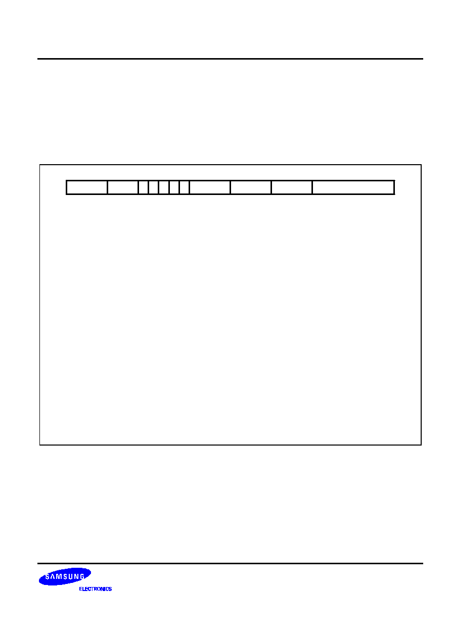
S3C2501X
INSTRUCTION SET
3-53
3.15 COPROCESSOR DATA TRANSFERS (LDC, STC)
The instruction is only executed if the condition is true. The various conditions are defined in Table 3-2. The
instruction encoding is shown in Figure 3-26.
This class of instruction is used to load (LDC) or store (STC) a subset of a coprocessor's registers directly to
memory. ARM9TDMI is responsible for supplying the memory address, and the coprocessor supplies or accepts
the data and controls the number of words transferred.
[7:0] Unsigned 8 Bit Immediate Offset
[11:8] Coprocessor Number
[15:12] Coprocessor Source/Destination Register
[19:16] Base Register
[20] Load/Store Bit
0 = Store to memory
1 = Load from memory
[21] Write-back Bit
0 = No write-back
1 = Write address into base
[22] Transfer Length
[23] Up/Down Bit
0 = Down: subtract offset from base
1 = Up: add offset to base
[24] Pre/Post Indexing Bit
0 = Post: add offset after transfer
1 = Pre: add offset bofore transfer
[31:28] Condition Field
31
27
19
15
Cond
28
16
11
12
21
23
N
20
L
Rn
CRd
22
110
P U
CP#
W
24
25
Offset
8 7
0
Figure 3-26. Coprocessor Data Transfer Instructions
3.15.1 THE COPROCESSOR FIELDS
The CP# field is used to identify the coprocessor which is required to supply or accept the data, and a
coprocessor will only respond if its number matches the contents of this field.
The CRd field and the N bit contain information for the coprocessor which may be interpreted in different ways by
different coprocessors, but by convention CRd is the register to be transferred (or the first register where more
than one is to be transferred), and the N bit is used to choose one of two transfer length options. For instance N =
0 could select the transfer of a single register, and N = 1 could select the transfer of all the registers for context
switching.

INSTRUCTION SET
S3C2501X
3-54
3.15.2 ADDRESSING MODES
ARM9TDMI is responsible for providing the address used by the memory system for the transfer, and the
addressing modes available are a subset of those used in single data transfer instructions. Note, however, that
the immediate offsets are 8 bits wide and specify word offsets for coprocessor data transfers, whereas they are
12 bits wide and specify byte offsets for single data transfers.
The 8 bit unsigned immediate offset is shifted left 2 bits and either added to (U = 1) or subtracted from (U = 0)
the base register (Rn); this calculation may be performed either before (P = 1) or after (P = 0) the base is used as
the transfer address. The modified base value may be overwritten back into the base register (if W = 1), or the
old value of the base may be preserved (W = 0). Note that post-indexed addressing modes require explicit
setting of the W bit, unlike LDR and STR which always write-back when post-indexed.
The value of the base register, modified by the offset in a pre-indexed instruction, is used as the address for the
transfer of the first word. The second word (if more than one is transferred) will go to or come from an address
one word (4 bytes) higher than the first transfer, and the address will be incremented by one word for each
subsequent transfer.
3.15.3 ADDRESS ALIGNMENT
The base address should normally be a word aligned quantity. The bottom 2 bits of the address will appear on
A[1:0] and might be interpreted by the memory system.
3.15.4 USE OF R15
If Rn is R15, the value used will be the address of the instruction plus 8 bytes. Base write-back to R15 must not
be specified.
3.15.5 DATA ABORTS
If the address is legal but the memory manager generates an abort, the data trap will be taken. The write-back of
the modified base will take place, but all other processor state will be preserved. The coprocessor is partly
responsible for ensuring that the data transfer can be restarted after the cause of the abort has been resolved,
and must ensure that any subsequent actions it undertakes can be repeated when the instruction is retried.
3.15.6 INSTRUCTION CYCLE TIMES
Coprocessor data transfer instructions take (n-1)S + 2N + bI incremental cycles to execute, where:
N
The number of words transferred.
B
The number of cycles spent in the coprocessor busy-wait loop.
S, N and I are defined as sequential (S-cycle), non-sequential (N-cycle), and internal (I-cycle), respectively.

S3C2501X
INSTRUCTION SET
3-55
3.15.7 ASSEMBLER SYNTAX
<LDC|STC>{cond}{L} p#,cd,<Address>
LDC
Load from memory to coprocessor
STC
Store from coprocessor to memory
{L}
When present perform long transfer (N = 1), otherwise perform short transfer
(N = 0)
{cond}
Two character condition mnemonic. See Table 3-2.
p#
The unique number of the required coprocessor
Cd
An expression evaluating to a valid coprocessor register number that is placed in
the CRd field
<Address> can be:
1
An expression which generates an address:
The assembler will attempt to generate an instruction using the PC as a base and a
corrected immediate offset to address the location given by evaluating the
expression. This will be a PC relative, pre-indexed address. If the address is out of
range, an error will be generated
2
A pre-indexed addressing specification:
[Rn]
offset of zero
[Rn,<#expression>]{!}
offset of <expression> bytes
A post-indexed addressing specification:
Rn],<#expression
offset of <expression> bytes
{!}
write back the base register (set the W bit) if! is
present
Rn
is an expression evaluating to a valid
ARM9TDMI register number.
NOTE
If Rn is R15, the assembler will subtract 8 from the offset value to allow for ARM9TDMI pipelining.
Examples
LDC
p1,c2,table
; Load c2 of coproc 1 from address
; table, using a PC relative address.
STCEQL
p2,c3,[R5,#24]!
; Conditionally store c3 of coproc 2
; into an address 24 bytes up from R5,
; write this address back to R5, and use
; long transfer option (probably to store multiple words).
NOTE
Although the address offset is expressed in bytes, the instruction offset field is in words. The assembler
will adjust the offset appropriately.

INSTRUCTION SET
S3C2501X
3-56
3.16 COPROCESSOR REGISTER TRANSFERS (MRC, MCR)
The instruction is only executed if the condition is true. The various conditions are defined in Table 3-2.. The
instruction encoding is shown in Figure 3-27.
This class of instruction is used to communicate information directly between ARM9TDMI and a coprocessor. An
example of a coprocessor to ARM9TDMI register transfer (MRC) instruction would be a FIX of a floating point
value held in a coprocessor, where the floating point number is converted into a 32 bit integer within the
coprocessor, and the result is then transferred to ARM9TDMI register. A FLOAT of a 32 bit value in ARM9TDMI
register into a floating point value within the coprocessor illustrates the use of ARM9TDMI register to coprocessor
transfer (MCR).
An important use of this instruction is to communicate control information directly from the coprocessor into the
ARM9TDMI CPSR flags. As an example, the result of a comparison of two floating point values within a
coprocessor can be moved to the CPSR to control the subsequent flow of execution.
31
27
19
15
Cond
28
16
11
12
21
23
20
L
CRn
Rd
[3:0] Coprocessor Operand Register
[7:5] Coprocessor Information
[11:8] Coprocessor Number
[15:12] ARM Source/Destination Register
[19:16] Coprocessor Source/Destination Register
[20] Load/Store Bit
0 = Store to coprocessor
1 = Load from coprocessor
[21] Coprocessor Operation Mode
[31:28] Condition Field
1110
CP Opc
CP#
24
CRm
1
CP
8 7
5 4 3
0
Figure 3-27. Coprocessor Register Transfer Instructions
3.16.1 THE COPROCESSOR FIELDS
The CP# field is used, as for all coprocessor instructions, to specify which coprocessor is being called upon.
The CP Opc, CRn, CP and CRm fields are used only by the coprocessor, and the interpretation presented here is
derived from convention only. Other interpretations are allowed where the coprocessor functionality is
incompatible with this one. The conventional interpretation is that the CP Opc and CP fields specify the operation
the coprocessor is required to perform, CRn is the coprocessor register which is the source or destination of the
transferred information, and CRm is a second coprocessor register which may be involved in some way which
depends on the particular operation specified.

S3C2501X
INSTRUCTION SET
3-57
3.16.2 TRANSFERS TO R15
When a coprocessor register transfer to ARM9TDMI has R15 as the destination, bits 31, 30, 29 and 28 of the
transferred word are copied into the N, Z, C and V flags respectively. The other bits of the transferred word are
ignored, and the PC and other CPSR bits are unaffected by the transfer.
3.16.3 TRANSFERS FROM R15
A coprocessor register transfer from ARM9TDMI with R15 as the source register will store the PC+ 12.
3.16.4 INSTRUCTION CYCLE TIMES
MRC instructions take 1S + (b+1)I +1C incremental cycles to execute, where S, I and C are defined as sequential
(S-cycle), internal (I-cycle), and coprocessor register transfer (C-cycle), respectively. MCR instructions take 1S +
bI +1C incremental cycles to execute, where b is the number of cycles spent in the coprocessor busy-wait loop.
3.16.5 ASSEMBLER SYNTAX
<MCR|MRC>{cond} p#,<expression1>,Rd,cn,cm{,<expression2>}
MRC
Move from coprocessor to ARM9TDMI register (L = 1)
MCR
Move from ARM9TDMI register to coprocessor (L = 0)
{cond}
Two character condition mnemonic. See Table 3-2.
p#
The unique number of the required coprocessor
<expression1>
Evaluated to a constant and placed in the CP Opc field
Rd
An expression evaluating to a valid ARM9TDMI register number
cn and cm
Expressions evaluating to the valid coprocessor register numbers CRn and CRm
respectively
<expression2>
Where present is evaluated to a constant and placed in the CP field
Examples
MRC
p2,5,R3,c5,c6
; Request coproc 2 to perform operation 5
; on c5 and c6, and transfer the (single
; 32-bit word) result back to R3.
MCR
p6,0,R4,c5,c6
; Request coproc 6 to perform operation 0
; on R4 and place the result in c6.
MRCEQ
p3,9,R3,c5,c6,2
; Conditionally request coproc 3 to
; perform operation 9 (type 2) on c5 and
; c6, and transfer the result back to R3.

INSTRUCTION SET
S3C2501X
3-58
3.17 UNDEFINED INSTRUCTION
The instruction is only executed if the condition is true. The various conditions are defined in Table 3-2. The
instruction format is shown in Figure 3-28.
31
27
Cond
28
25 24
011
xxxxxxxxxxxxxxxxxxxx
1
xxxx
5 4 3
0
Figure 3-28. Undefined Instruction
If the condition is true, the undefined instruction trap will be taken.
Note that the undefined instruction mechanism involves offering this instruction to any coprocessors which may
be present, and all coprocessors must refuse to accept it by driving CPA and CPB HIGH.
3.17.1 INSTRUCTION CYCLE TIMES
This instruction takes 2S + 1I + 1N cycles, where S, N and I are defined as sequential (S-cycle), non-sequential
(N-cycle), and internal (I-cycle).
3.17.2 ASSEMBLER SYNTAX
The assembler has no mnemonics for generating this instruction. If it is adopted in the future for some specified
use, suitable mnemonics will be added to the assembler. Until such time, this instruction must not be used.

S3C2501X
INSTRUCTION SET
3-59
3.18 INSTRUCTION SET EXAMPLES
The following examples show ways in which the basic ARM9TDMI instructions can combine to give efficient
code. None of these methods saves a great deal of execution time (although they may save some), mostly they
just save code.
3.18.1 USING THE CONDITIONAL INSTRUCTIONS
Using Conditionals for Logical OR
CMP
Rn,#p
; If Rn=p OR Rm=q THEN GOTO Label.
BEQ
Label
CMP
Rm,#q
BEQ
Label
This can be replaced by
CMP
Rn,#p
CMPNE
Rm,#q
; If condition not satisfied try other test.
BEQ
Label
Absolute Value
TEQ
Rn,#0
; Test sign
RSBMI
Rn,Rn,#0
; and 2's complement if necessary.
Multiplication by 4, 5 or 6 (Run Time)
MOV
Rc,Ra,LSL#2
; Multiply by 4,
CMP
Rb,#5
; Test value,
ADDCS
Rc,Rc,Ra
; Complete multiply by 5,
ADDHI
Rc,Rc,Ra
; Complete multiply by 6.
Combining Discrete and Range Tests
TEQ
Rc,#127
; Discrete test,
CMPNE
Rc, # " " - 1
; Range test
MOVLS
Rc,# " "
; IF Rc<= " " OR Rc=ASCII(127)
; THEN Rc:= " "

INSTRUCTION SET
S3C2501X
3-60
Division and Remainder
A number of divide routines for specific applications are provided in source form as part of the ANSI C library
provided with the ARM Cross development toolkit, available from your supplier. A short general purpose divide
routine follows.
; Enter with numbers in Ra and Rb.
MOV
Rcnt,#1
; Bit to control the division.
Div1
CMP
Rb,#0x80000000
; Move Rb until greater than Ra.
CMPCC
Rb,Ra
MOVCC
Rb,Rb,ASL#1
MOVCC
Rcnt,Rcnt,ASL#1
BCC
Div1
MOV
Rc,#0
Div2
CMP
Ra,Rb
; Test for possible subtraction.
SUBCS
Ra,Ra,Rb
; Subtract if ok,
ADDCS
Rc,Rc,Rcnt
; Put relevant bit into result
MOVS
Rcnt,Rcnt,LSR#1
; Shift control bit
MOVNE
Rb,Rb,LSR#1
; Halve unless finished.
BNE
Div2
; Divide result in Rc, remainder in Ra.
Overflow Detection in the ARM9TDMI
1. Overflow in unsigned multiply with a 32-bit result
UMULL
Rd,Rt,Rm,Rn
; 3 to 6 cycles
TEQ
Rt,#0
; +1 cycle and a register
BNE
overflow
2. Overflow in signed multiply with a 32-bit result
SMULL
Rd,Rt,Rm,Rn
; 3 to 6 cycles
TEQ
Rt,Rd ASR#31
; +1 cycle and a register
BNE
overflow
3. Overflow in unsigned multiply accumulate with a 32 bit result
UMLAL
Rd,Rt,Rm,Rn
; 4 to 7 cycles
TEQ
Rt,#0
; +1 cycle and a register
BNE
overflow
4. Overflow in signed multiply accumulate with a 32 bit result
SMLAL
Rd,Rt,Rm,Rn
; 4 to 7 cycles
TEQ
Rt,Rd, ASR#31
; +1 cycle and a register
BNE
overflow

S3C2501X
INSTRUCTION SET
3-61
5. Overflow in unsigned multiply accumulate with a 64 bit result
UMULL
Rl,Rh,Rm,Rn
; 3 to 6 cycles
ADDS
Rl,Rl,Ra1
; Lower accumulate
ADC
Rh,Rh,Ra2
; Upper accumulate
BCS
overflow
; 1 cycle and 2 registers
6. Overflow in signed multiply accumulate with a 64 bit result
SMULL
Rl,Rh,Rm,Rn
; 3 to 6 cycles
ADDS
Rl,Rl,Ra1
; Lower accumulate
ADC
Rh,Rh,Ra2
; Upper accumulate
BVS
overflow
; 1 cycle and 2 registers
NOTE
Overflow checking is not applicable to unsigned and signed multiplies with a 64-bit result, since overflow
does not occur in such calculations.
3.18.2 PSEUDO-RANDOM BINARY SEQUENCE GENERATOR
It is often necessary to generate (pseudo-) random numbers and the most efficient algorithms are based on shift
generators with exclusive-OR feedback rather like a cyclic redundancy check generator. Unfortunately the
sequence of a 32 bit generator needs more than one feedback tap to be maximal length (i.e. 2^32-1 cycles
before repetition), so this example uses a 33 bit register with taps at bits 33 and 20. The basic algorithm is
newbit: = bit 33 eor bit 20, shift left the 33 bit number and put in newbit at the bottom; this operation is performed
for all the newbits needed (i.e. 32 bits). The entire operation can be done in 5 S cycles:
; Enter with seed in Ra (32 bits),
; Rb (1 bit in Rb lsb), uses Rc.
TST
Rb,Rb,LSR#1
; Top bit into carry
MOVS
Rc,Ra,RRX
; 33 bit rotate right
ADC
Rb,Rb,Rb
; Carry into lsb of Rb
EOR
Rc,Rc,Ra,LSL#12
; (involved!)
EOR
Ra,Rc,Rc,LSR#20
; (similarly involved!) new seed in Ra, Rb as before
3.18.3 MULTIPLICATION BY CONSTANT USING THE BARREL SHIFTER
Multiplication by 2^n (1,2,4,8,16,32..)
MOV
Ra, Rb, LSL #n
Multiplication by 2^n+1 (3,5,9,17..)
ADD
Ra,Ra,Ra,LSL #n
Multiplication by 2^n-1 (3,7,15..)
RSB
Ra,Ra,Ra,LSL #n

INSTRUCTION SET
S3C2501X
3-62
Multiplication by 6
ADD
Ra,Ra,Ra,LSL #1
; Multiply by 3
MOV
Ra,Ra,LSL#1
; and then by 2
Multiply by 10 and add in extra number
ADD
Ra,Ra,Ra,LSL#2
; Multiply by 5
ADD
Ra,Rc,Ra,LSL#1
; Multiply by 2 and add in next digit
General recursive method for Rb := Ra*C, C a constant:
1. If C even, say C = 2^n*D, D odd:
D=1:
MOV Rb,Ra,LSL #n
D<>1:
{Rb := Ra*D}
MOV
Rb,Rb,LSL #n
2. If C MOD 4 = 1, say C = 2^n*D+1, D odd, n>1:
D=1:
ADD Rb,Ra,Ra,LSL #n
D<>1:
{Rb := Ra*D}
ADD
Rb,Ra,Rb,LSL #n
3. If C MOD 4 = 3, say C = 2^n*D-1, D odd, n>1:
D=1:
RSB Rb,Ra,Ra,LSL #n
D<>1:
{Rb := Ra*D}
RSB
Rb,Ra,Rb,LSL #n
This is not quite optimal, but close. An example of its non-optimality is multiply by 45 which is done by:
RSB
Rb,Ra,Ra,LSL#2
; Multiply by 3
RSB
Rb,Ra,Rb,LSL#2
; Multiply by 4*3-1 = 11
ADD
Rb,Ra,Rb,LSL# 2
; Multiply by 4*11+1 = 45
rather than by:
ADD
Rb,Ra,Ra,LSL#3
; Multiply by 9
ADD
Rb,Rb,Rb,LSL#2
; Multiply by 5*9 = 45

S3C2501X
INSTRUCTION SET
3-63
3.18.4 LOADING A WORD FROM AN UNKNOWN ALIGNMENT
; Enter with address in Ra (32 bits) uses
; Rb, Rc result in Rd. Note d must be less than c e.g. 0,1
BIC
Rb,Ra,#3
; Get word aligned address
LDMIA
Rb,{Rd,Rc}
; Get 64 bits containing answer
AND
Rb,Ra,#3
; Correction factor in bytes
MOVS
Rb,Rb,LSL#3
; ...now in bits and test if aligned
MOVNE
Rd,Rd,LSR Rb
; Produce bottom of result word (if not aligned)
RSBNE
Rb,Rb,#32
; Get other shift amount
ORRNE
Rd,Rd,Rc,LSL Rb
; Combine two halves to get result

INSTRUCTION SET
S3C2501X
3-64
3.19 THUMB INSTRUCTION SET FORMAT
The thumb instruction sets are 16-bit versions of ARM instruction sets (32-bit format). The ARM instructions are
reduced to 16-bit versions, Thumb instructions, at the cost of versatile functions of the ARM instruction sets. The
thumb instructions are decompressed to the ARM instructions by the Thumb decompressor inside the
ARM9TDMI core.
As the Thumb instructions are compressed ARM instructions, the Thumb instructions have the 16-bit format
instructions and have some restrictions. The restrictions by 16-bit format is fully notified for using the Thumb
instructions.
3.19.1 FORMAT SUMMARY
The THUMB instruction set formats are shown in the following figure.
Move Shifted register
0
0
0
0
0
0
0
0
0
0
0
0
1
0
0
0
1
0
0
0
0
0
0
1
1
1
1
1
1
1
0
0
0
0
0
1
1
1
1
1
1
1
1
0
L
0
1
1
1
1
1
1
1
1
1
1
1
1
1
1
1
1
0
0
0
0
1
1
1
1
0
0
1
0
0
L
1
0
R
1
1
0
1
0
SP
1
L
L
S
H
0
0
1
B
L
0
1
H
0
1
B
0
0
1
1
1
I
Op
Op
Op
Op
Op
L
0
S
1
Offset5
Rs
Rd
Rn/offset3
Rd
Rs
Rd
Offset8
Rs
Rd/Hd
Rd
H1 H2
Rs/Hs
Rd
Word8
Rd
Rb
Ro
Ro
Rb
Rd
Offset5
Rb
Rd
Rb
Rd
Offset5
Rd
Rd
Word8
Word8
SWord7
Rb
Cond
Rlist
Rlist
Softset8
Value8
Offset11
Offset
Add/subtract
Move/compare/add/
subtract immediate
ALU operations
Hi regiter operations
/branch exchange
PC-relative load
Load/store with register
offset
Load/store with immediate
offset
Load/store sign-extended
byte/halfword
Load/store halfword
SP-relative load/store
Load address
Add offset to stack pointer
Push/pop register
Multiple load/store
Conditional branch
Software interrupt
Unconditional branch
Long branch with link
15 14 13 12 11 10
9
8
7
6
5
4
2
3
1
0
15 14 13 12 11 10
9
8
7
6
5
4
2
3
1
0
1
2
3
4
5
6
7
8
9
10
11
12
13
14
15
16
17
18
19
Figure 3-29. THUMB Instruction Set Formats

S3C2501X
INSTRUCTION SET
3-65
3.19.2 OPCODE SUMMARY
The following table summarises the THUMB instruction set. For further information about a particular instruction
please refer to the sections listed in the right-most column.
Table 3-7. THUMB Instruction Set Opcodes
Mnemonic
Instruction
Lo-Register
Operand
Hi-Register
Operand
Condition
Codes Set
ADC
Add with carry
V
≠
V
ADD
Add
V
V
V
(1)
AND
AND
V
≠
V
ASR
Arithmetic shift right
V
≠
V
B
Unconditional branch
V
≠
≠
Bxx
Conditional branch
V
≠
≠
BIC
Bit clear
V
≠
V
BL
Branch and link
V
≠
≠
BX
Branch and exchange
V
V
≠
CMN
Compare negative
V
≠
V
CMP
Compare
V
V
V
EOR
EOR
V
≠
V
LDMIA
Load multiple
V
≠
≠
LDR
Load word
V
≠
≠
LDRB
Load byte
V
≠
≠
LDRH
Load half-word
V
≠
≠
LSL
Logical shift left
V
≠
V
LDSB
Load sign-extended byte
V
≠
≠
LDSH
Load sign-extended half-word
V
≠
≠
LSR
Logical shift right
V
≠
V
MOV
Move register
V
V
V
(2)
MUL
Multiply
V
≠
V
MVN
Move negative register
V
≠
V
NEG
Negate
V
≠
V
ORR
OR
V
≠
V
POP
Pop registers
V
≠
≠
PUSH
Push registers
V
≠
≠
POR
Rotate right
V
≠
V

INSTRUCTION SET
S3C2501X
3-66
Table 3-7. THUMB Instruction Set Opcodes (Continued)
Mnemonic
Instruction
Lo-Register
Operand
Hi-Register
Operand
Condition
Codes Set
SBC
Subtract with carry
V
≠
V
STMIA
Store multiple
V
≠
≠
STR
Store word
V
≠
≠
STRB
Store byte
V
≠
≠
STRH
Store half-word
V
≠
≠
SWI
Software interrupt
≠
≠
≠
SUB
Subtract
V
≠
V
TST
Test bits
V
≠
V
NOTES:
1.
The condition codes are unaffected by the format 5, 12 and 13 versions of this instruction.
2.
The condition codes are unaffected by the format 5 version of this instruction.

S3C2501X
INSTRUCTION SET
3-67
3.20 FORMAT 1: MOVE SHIFTED REGISTER
15
0
0
14
10
[2:0] Destination Register
[5:3] Source Register
[10:6] Immediate Vale
[12:11] Opcode
0 = LSL
1 = LSR
2 = ASR
Offset5
6
5
3
2
Rd
0
0
13
12
11
Op
Rs
Figure 3-30. Format 1
3.20.1 OPERATION
These instructions move a shifted value between Lo registers. The THUMB assembler syntax is shown in
Table 3-8.
NOTE
All instructions in this group set the CPSR condition codes.
Table 3-8. Summary of Format 1 Instructions
OP
THUMB Assembler
ARM Equivalent
Action
00
LSL Rd, Rs, #Offset5
MOVS Rd, Rs, LSL #Offset5
Shift Rs left by a 5-bit immediate value and
store the result in Rd.
01
LSR Rd, Rs, #Offset5
MOVS Rd, Rs, LSR #Offset5
Perform logical shift right on Rs by a 5-bit
immediate value and store the result in Rd.
10
ASR Rd, Rs, #Offset5
MOVS Rd, Rs, ASR #Offset5
Perform arithmetic shift right on Rs by a 5-bit
immediate value and store the result in Rd.
3.20.2 INSTRUCTION CYCLE TIMES
All instructions in this format have an equivalent ARM instruction as shown in Table 3-8. The instruction cycle
times for the THUMB instruction are identical to that of the equivalent ARM instruction.
Examples
LSR
R2, R5, #27
; Logical shift right the contents
; of R5 by 27 and store the result in R2.
; Set condition codes on the result.

INSTRUCTION SET
S3C2501X
3-68
3.21 FORMAT 2: ADD/SUBTRACT
15
0
14
10
[2:0] Destination Register
[5:3] Source Register
[8:6] Register/Immediate Value
[9] Opcode
0 = ADD
1 = SUB
[10] Immediate Flag
0 = Register operand
1 = Immediate oerand
Rn/Offset3
Rd
0
0
13
12
11
Op
Rs
9
8
1
1
1
6
5
3
2
0
Figure 3-31. Format 2
3.21.1 OPERATION
These instructions allow the contents of a Lo register or a 3-bit immediate value to be added to or subtracted
from a Lo register. The THUMB assembler syntax is shown in Table 3-9.
NOTE
All instructions in this group set the CPSR condition codes.
Table 3-9. Summary of Format 2 Instructions
OP
I
THUMB Assembler
ARM Equivalent
Action
0
0
ADD Rd, Rs, Rn
ADDS Rd, Rs, Rn
Add contents of Rn to contents of Rs.
Place result in Rd.
0
1
ADD Rd, Rs, #Offset3
ADDS Rd, Rs, #Offset3
Add 3-bit immediate value to contents of Rs.
Place result in Rd.
1
0
SUB Rd, Rs, Rn
SUBS Rd, Rs, Rn
Subtract contents of Rn from contents of Rs.
Place result in Rd.
1
1
SUB Rd, Rs, #Offset3
SUBS Rd, Rs, #Offset3
Subtract 3-bit immediate value from contents
of Rs. Place result in Rd.

S3C2501X
INSTRUCTION SET
3-69
3.21.2 INSTRUCTION CYCLE TIMES
All instructions in this format have an equivalent ARM instruction as shown in Table 3-9. The instruction cycle
times for the THUMB instruction are identical to that of the equivalent ARM instruction.
Examples
ADD
R0, R3, R4
; R0 : = R3 + R4 and set condition codes on the result.
SUB
R6, R2, #6
; R6 : = R2 - 6 and set condition codes.

INSTRUCTION SET
S3C2501X
3-70
3.22 FORMAT 3: MOVE/COMPARE/ADD/SUBTRACT IMMEDIATE
15
0
0
14
10
[7:0] Immediate Value
[10:8] Source/Destination Register
[12:11] Opcode
0 = MOV
1 = CMP
2 = ADD
3 = SUB
Offset8
Rd
0
0
13
12
11
Op
7
8
Figure 3-32. Format 3
3.22.1 OPERATIONS
The instructions in this group perform operations between a Lo register and an 8-bit immediate value. The
THUMB assembler syntax is shown in Table 3-10.
NOTE
All instructions in this group set the CPSR condition codes.
Table 3-10. Summary of Format 3 Instructions
OP
THUMB Assembler
ARM Equivalent
Action
00
MOV Rd, #Offset8
MOVS Rd, #Offset8
Move 8-bit immediate value into Rd.
01
CMP Rd, #Offset8
CMP Rd, #Offset8
Compare contents of Rd with 8-bit immediate
value.
10
ADD Rd, #Offset8
ADDS Rd, Rd, #Offset8
Add 8-bit immediate value to contents of Rd and
place the result in Rd.
11
SUB Rd, #Offset8
SUBS Rd, Rd, #Offset8
Subtract 8-bit immediate value from contents of
Rd and place the result in Rd.
3.22.2 INSTRUCTION CYCLE TIMES
All instructions in this format have an equivalent ARM instruction as shown in Table 3-10. The instruction cycle
times for the THUMB instruction are identical to that of the equivalent ARM instruction.
Examples
MOV
R0, #128
; R0 : = 128 and set condition codes
CMP
R2, #62
; Set condition codes on R2 - 62
ADD
R1, #255
; R1 : = R1 + 255 and set condition codes
SUB
R6, #145
; R6 : = R6 - 145 and set condition codes

S3C2501X
INSTRUCTION SET
3-71
3.23 FORMAT 4: ALU OPERATIONS
15
0
0
14
10
[2:0] Source/Destination Register
[5:3] Source Register 2
[9:6] Opcode
5
6
3
Rd
0
0
13
12
11
Op
Rs
0
0
0
9
2
Figure 3-33. Format 4
3.23.1 OPERATION
The following instructions perform ALU operations on a Lo register pair.
NOTE
All instructions in this group set the CPSR condition codes
Table 3-11. Summary of Format 4 Instructions
OP
THUMB Assembler
ARM Equivalent
Action
0000
AND Rd, Rs
ANDS Rd, Rd, Rs
Rd: = Rd AND Rs
0001
EOR Rd, Rs
EORS Rd, Rd, Rs
Rd: = Rd EOR Rs
0010
LSL Rd, Rs
MOVS Rd, Rd, LSL Rs
Rd : = Rd << Rs
0011
LSR Rd, Rs
MOVS Rd, Rd, LSR Rs
Rd : = Rd >> Rs
0100
ASR Rd, Rs
MOVS Rd, Rd, ASR Rs
Rd : = Rd ASR Rs
0101
ADC Rd, Rs
ADCS Rd, Rd, Rs
Rd : = Rd + Rs + C-bit
0110
SBC Rd, Rs
SBCS Rd, Rd, Rs
Rd : = Rd - Rs - NOT C-bit
0111
ROR Rd, Rs
MOVS Rd, Rd, ROR Rs
Rd : = Rd ROR Rs
1000
TST Rd, Rs
TST Rd, Rs
Set condition codes on Rd AND Rs
1001
NEG Rd, Rs
RSBS Rd, Rs, #0
Rd = - Rs
1010
CMP Rd, Rs
CMP Rd, Rs
Set condition codes on Rd - Rs
1011
CMN Rd, Rs
CMN Rd, Rs
Set condition codes on Rd + Rs
1100
ORR Rd, Rs
ORRS Rd, Rd, Rs
Rd: = Rd OR Rs
1101
MUL Rd, Rs
MULS Rd, Rs, Rd
Rd: = Rs * Rd
1110
BIC Rd, Rs
BICS Rd, Rd, Rs
Rd: = Rd AND NOT Rs
1111
MVN Rd, Rs
MVNS Rd, Rs
Rd: = NOT Rs

INSTRUCTION SET
S3C2501X
3-72
3.23.2 INSTRUCTION CYCLE TIMES
All instructions in this format have an equivalent ARM instruction as shown in Table 3-11. The instruction cycle
times for the THUMB instruction are identical to that of the equivalent ARM instruction.
Examples
EOR
R3, R4
; R3 : = R3 EOR R4 and set condition codes
ROR
R1, R0
; Rotate right R1 by the value in R0, store
; the result in R1 and set condition codes
NEG
R5, R3
; Subtract the contents of R3 from zero,
; store the result in R5. Set condition codes ie R5 = - R3
CMP
R2, R6
; Set the condition codes on the result of R2 - R6
MUL
R0, R7
; R0 : = R7 * R0 and set condition codes

S3C2501X
INSTRUCTION SET
3-73
3.24 FORMAT 5: HI-REGISTER OPERATIONS/BRANCH EXCHANGE
15
0
0
14
10
[2:0] Destination Register
[5:3] Source Register
[6] Hi Operand Flag 2
[7] Hi Operand Flag 1
[9:8] Opcode
6
5
3
2
Rd/Hd
0
0
13
12
11
Op
Rs/Hs
0
0
0
9
8
7
H1
H2
Figure 3-34. Format 5
3.24.1 OPERATION
There are four sets of instructions in this group. The first three allow ADD, CMP and MOV operations to be
performed between Lo and Hi registers, or a pair of Hi registers. The fourth, BX, allows a Branch to be performed
which may also be used to switch processor state. The THUMB assembler syntax is shown in Table 3-12.
NOTE
In this group only CMP (Op = 01) sets the CPSR condition codes.
The action of H1 = 0, H2 = 0 for Op = 00 (ADD), Op = 01 (CMP) and Op = 10 (MOV) is undefined, and should
not be used.

INSTRUCTION SET
S3C2501X
3-74
Table 3-12. Summary of Format 5 Instructions
OP
H1
H2
THUMB Assembler
ARM Equivalent
Action
00
0
1
ADD Rd, Hs
ADD Rd, Rd, Hs
Add a register in the range 8-15 to a register in
the range 0-7.
00
1
0
ADD Hd, Rs
ADD Hd, Hd, Rs
Add a register in the range 0-7 to a register in
the range 8-15.
00
1
1
ADD Hd, Hs
ADD Hd, Hd, Hs
Add two registers in the range 8-15.
01
0
1
CMP Rd, Hs
CMP Rd, Hs
Compare a register in the range 0-7 with a
register in the range 8-15. Set the condition
code flags on the result.
01
1
0
CMP Hd, Rs
CMP Hd, Rs
Compare a register in the range 8-15 with a
register in the range 0-7. Set the condition
code flags on the result.
01
1
1
CMP Hd, Hs
CMP Hd, Hs
Compare two registers in the range 8-15. Set
the condition code flags on the result.
10
0
1
MOV Rd, Hs
MOV Rd, Hs
Move a value from a register in the range 8-15
to a register in the range 0-7.
10
1
0
MOV Hd, Rs
MOV Hd, Rs
Move a value from a register in the range 0-7
to a register in the range 8-15.
00
0
1
MOV Hd, Hs
MOV Hd, Hs
Move a value between two registers in the
range 8-15.
00
1
0
BX Rs
BX Rs
Perform branch (plus optional state change) to
address in a register in the range 0-7.
00
1
1
BX Hs
BX Hs
Perform branch (plus optional state change) to
address in a register in the range 8-15.
3.24.2 INSTRUCTION CYCLE TIMES
All instructions in this format have an equivalent ARM instruction as shown in Table 3-12. The instruction cycle
times for the THUMB instruction are identical to that of the equivalent ARM instruction.
3.24.3 THE BX INSTRUCTION
BX performs a branch to a routine whose start address is specified in a Lo or Hi register.
Bit 0 of the address determines the processor state on entry to the routine:
Bit 0 = 0
Causes the processor to enter ARM state.
Bit 0 = 1
Causes the processor to enter THUMB state.
NOTE
The action of H1 = 1 for this instruction is undefined, and should not be used.

S3C2501X
INSTRUCTION SET
3-75
Examples
Hi-Register Operations
ADD
PC, R5
; PC := PC + R5 but don't set the condition codes.CMP
R4, R12
; Set the condition codes on the result of R4 - R12.
MOV
R15, R14
; Move R14 (LR) into R15 (PC)
; but don't set the condition codes,
; eg. return from subroutine.
Branch and Exchange
; Switch from THUMB to ARM state.
ADR
R1,outofTHUMB
; Load address of outofTHUMB into R1.
MOV
R11,R1
BX
R11
; Transfer the contents of R11 into the PC.
; Bit 0 of R11 determines whether
; ARM or THUMB state is entered, ie. ARM state here.
...
ALIGN
CODE32
outofTHUMB
; Now processing ARM instructions...
3.24.4 USING R15 AS AN OPERAND
If R15 is used as an operand, the value will be the address of the instruction + 4 with bit 0 cleared. Executing a
BX PC in THUMB state from a non-word aligned address will result in unpredictable execution.

INSTRUCTION SET
S3C2501X
3-76
3.25 FORMAT 6: PC-RELATIVE LOAD
15
0
0
14
10
[7:0] Immediate Value
[10:8] Destination Register
Word 8
0
0
13
12
11
Rd
0
0
8
7
Figure 3-35. Format 6
3.25.1 OPERATION
This instruction loads a word from an address specified as a 10-bit immediate offset from the PC. The THUMB
assembler syntax is shown below.
Table 3-13. Summary of PC-Relative Load Instruction
THUMB Assembler
ARM Equivalent
Action
LDR Rd, [PC, #Imm]
LDR Rd, [R15, #Imm]
Add unsigned offset (255 words, 1020 bytes) in
Imm to the current value of the PC. Load the
word from the resulting address into Rd.
NOTE: The value specified by #Imm is a full 10-bit address, but must always be word-aligned (ie with bits 1:0 set to 0),
since the assembler places #Imm >> 2 in field Word 8. The value of the PC will be 4 bytes greater than
the address of this instruction, but bit 1 of the PC is forced to 0 to ensure it is word aligned.
3.25.2 INSTRUCTION CYCLE TIMES
All instructions in this format have an equivalent ARM instruction. The instruction cycle times for the THUMB
instruction are identical to that of the equivalent ARM instruction.
Examples
LDR R3,[PC,#844]
; Load into R3 the word found at the
; address formed by adding 844 to PC.
; bit[1] of PC is forced to zero.
; Note that the THUMB opcode will contain
; 211 as the Word8 value.

S3C2501X
INSTRUCTION SET
3-77
3.26 FORMAT 7: LOAD/STORE WITH REGISTER OFFSET
[2:0] Source/Destination Register
[5:3] Base Register
[8:6] Offset Register
[10] Byte/Word Flag
0 = Transfer word quantity
1 = Transfer byte quantity
[11] Load/Store Flag
0 = Store to memory
1 = Load from memory
15
0
0
14
10
6
5
3
2
Rd
1
0
13
12
11
Rb
1
L
B
9
8
Ro
0
Figure 3-36. Format 7
3.26.1 OPERATION
These instructions transfer byte or word values between registers and memory. Memory addresses are pre-
indexed using an offset register in the range 0-7. The THUMB assembler syntax is shown in Table 3-14.
Table 3-14. Summary of Format 7 Instructions
L
B
THUMB Assembler
ARM Equivalent
Action
0
0
STR Rd, [Rb, Ro]
STR Rd, [Rb, Ro]
Pre-indexed word store:
Calculate the target address by adding together the
value in Rb and the value in Ro. Store the contents of
Rd at the address.
0
1
STRB Rd, [Rb, Ro]
STRB Rd, [Rb, Ro]
Pre-indexed byte store:
Calculate the target address by adding together the
value in Rb and the value in Ro. Store the byte value
in Rd at the resulting address.
1
0
LDR Rd, [Rb, Ro]
LDR Rd, [Rb, Ro]
Pre-indexed word load:
Calculate the source address by adding together the
value in Rb and the value in Ro. Load the contents of
the address into Rd.
1
1
LDRB Rd, [Rb, Ro]
LDRB Rd, [Rb, Ro]
Pre-indexed byte load:
Calculate the source address by adding together the
value in Rb and the value in Ro. Load the byte value
at the resulting address.

INSTRUCTION SET
S3C2501X
3-78
3.26.2 INSTRUCTION CYCLE TIMES
All instructions in this format have an equivalent ARM instruction as shown in Table 3-14. The instruction cycle
times for the THUMB instruction are identical to that of the equivalent ARM instruction.
Examples
STR
R3, [R2,R6]
; Store word in R3 at the address
; formed by adding R6 to R2.
LDRB
R2, [R0,R7]
; Load into R2 the byte found at
; the address formed by adding R7 to R0.

S3C2501X
INSTRUCTION SET
3-79
3.27 FORMAT 8: LOAD/STORE SIGN-EXTENDED BYTE/HALF-WORD
[2:0] Destination Register
[5:3] Base Register
[8:6] Offset Register
[10] Sign-Extended Flag
0 = Operand not sing-extended
1 = Operand sing-extended
[11] H Flag
15
0
0
14
10
6
5
3
2
Rd
1
0
13
12
11
Rb
1
H
S
9
8
Ro
1
Figure 3-37. Format 8
3.27.1 OPERATION
These instructions load optionally sign-extended bytes or half-words, and store half-words. The THUMB
assembler syntax is shown below.
Table 3-15. Summary of format 8 instructions
L
B
THUMB Assembler
ARM Equivalent
Action
0
0
STRH Rd, [Rb, Ro]
STRH Rd, [Rb, Ro]
Store half-word:
Add Ro to base address in Rb. Store bits 0≠15 of Rd at
the resulting address.
0
1
LDRH Rd, [Rb, Ro]
LDRH Rd, [Rb, Ro]
Load half-word:
Add Ro to base address in Rb. Load bits 0≠15 of Rd from
the resulting address, and set bits 16-31 of Rd to 0.
1
0
LDSB Rd, [Rb, Ro]
LDRSB Rd, [Rb, Ro]
Load sign-extended byte:
Add Ro to base address in Rb. Load bits 0≠7 of Rd from
the resulting address, and set bits 8-31 of Rd to bit 7.
1
1
LDSH Rd, [Rb, Ro]
LDRSH Rd, [Rb, Ro]
Load sign-extended half-word:
Add Ro to base address in Rb. Load bits 0≠15 of Rd from
the resulting address, and set bits 16-31 of Rd to bit 15.

INSTRUCTION SET
S3C2501X
3-80
3.27.2 INSTRUCTION CYCLE TIMES
All instructions in this format have an equivalent ARM instruction as shown in Table 3-15. The instruction cycle
times for the THUMB instruction are identical to that of the equivalent ARM instruction.
Examples
STRH
R4, [R3, R0]
; Store the lower 16 bits of R4 at the
; address formed by adding R0 to R3.
LDSB
R2, [R7, R1]
; Load into R2 the sign extended byte
; found at the address formed by adding R1 to R7.
LDSH
R3, [R4, R2]
; Load into R3 the sign extended half-word
; found at the address formed by adding R2 to R4.

S3C2501X
INSTRUCTION SET
3-81
3.28 FORMAT 9: LOAD/STORE WITH IMMEDIATE OFFSET
[2:0] Source/Destination Register
[5:3] Base Register
[10:6] Offset Register
[11] Load/Store Flag
0 = Store to memory
1 = Load from memory
[12] Byte/Word Flad
0 = Transfer word quantity
1 = Transfer byte quantity
15
0
0
14
10
6
5
3
2
Rd
1
1
13
12
11
Rb
B
L
Offset5
Figure 3-38. Format 9
3.28.1 OPERATION
These instructions transfer byte or word values between registers and memory using an immediate 5 or 7-bit offset. The
THUMB assembler syntax is shown in Table 3-16
Table 3-16. Summary of Format 9 Instructions
L
B
THUMB Assembler
ARM Equivalent
Action
0
0
STR Rd, [Rb, #Imm]
STR Rd, [Rb, #Imm]
Calculate the target address by adding together the
value in Rb and Imm. Store the contents of Rd at
the address.
0
1
LDR Rd, [Rb, #Imm]
LDR Rd, [Rb, #Imm]
Calculate the source address by adding together the
value in Rb and Imm. Load Rd from the address.
1
0
STRB Rd, [Rb, #Imm]
STRB Rd, [Rb, #Imm]
Calculate the target address by adding together the
value in Rb and Imm. Store the byte value in Rd at
the address.
1
1
LDRB Rd, [Rb, #Imm]
LDRB Rd, [Rb, #Imm]
Calculate source address by adding together the
value in Rb and Imm. Load the byte value at the
address into Rd.
NOTE: For word accesses (B = 0), the value specified by #Imm is a full 7-bit address, but must be word-aligned
(ie with bits 1:0 set to 0), since the assembler places #Imm >> 2 in the Offset5 field.

INSTRUCTION SET
S3C2501X
3-82
3.28.2 INSTRUCTION CYCLE TIMES
All instructions in this format have an equivalent ARM instruction as shown in Table 3-16. The instruction cycle
times for the THUMB instruction are identical to that of the equivalent ARM instruction.
Examples
LDR
R2, [R5,#116]
; Load into R2 the word found at the
; address formed by adding 116 to R5.
; Note that the THUMB opcode will
; contain 29 as the Offset5 value.
STRB
R1, [R0,#13]
; Store the lower 8 bits of R1 at the
; address formed by adding 13 to R0.
; Note that the THUMB opcode will
; contain 13 as the Offset5 value.

S3C2501X
INSTRUCTION SET
3-83
3.29 FORMAT 10: LOAD/STORE HALF-WORD
[2:0] Source/Destination Register
[5:3] Base Register
[10:6] Immediate Value
[11] Load/Store Flag
0 = Store to memory
1 = Load from memory
15
0
0
14
10
6
5
3
2
Rd
1
0
13
12
11
Rb
0
L
Offset5
Figure 3-39. Format 10
3.29.1 OPERATION
These instructions transfer half-word values between a Lo register and memory. Addresses are pre-indexed,
using a 6-bit immediate value. The THUMB assembler syntax is shown in Table 3-17.
Table 3-17. Half-word Data Transfer Instructions
L
THUMB Assembler
ARM Equivalent
Action
0
STRH Rd, [Rb, #Imm]
STRH Rd, [Rb, #Imm]
Add #Imm to base address in Rb and store bits 0≠15 of
Rd at the resulting address.
1
LDRH Rd, [Rb, #Imm]
LDRH Rd, [Rb, #Imm]
Add #Imm to base address in Rb. Load bits 0≠15 from the
resulting address into Rd and set bits 16-31 to zero.
NOTE: #Imm is a full 6-bit address but must be half-word-aligned (ie with bit 0 set to 0),
since the assembler places #Imm >> 1 in the Offset5 field.
3.29.2 INSTRUCTION CYCLE TIMES
All instructions in this format have an equivalent ARM instruction as shown in Table 3-17. The instruction cycle
times for the THUMB instruction are identical to that of the equivalent ARM instruction.
Examples
STRH
R6, [R1, #56]
; Store the lower 16 bits of R4 at the address formed by
; adding 56 R1. Note that the THUMB opcode will contain
; 28 as the Offset5 value.
LDRH
R4, [R7, #4]
; Load into R4 the half-word found at the address formed
by
; adding 4 to R7. Note that the THUMB opcode will
; contain 2 as the Offset5 value.

INSTRUCTION SET
S3C2501X
3-84
3.30 FORMAT 11: SP-RELATIVE LOAD/STORE
[7:0] Immediate Value
[10:8] Destination Register
[11] Load/Store Bit
0 = Store to memory
1 = Load from memory
15
0
1
14
10
0
0
13
12
11
Word 8
1
L
Rd
7
8
Figure 3-40. Format 11
3.30.1 OPERATION
The instructions in this group perform an SP-relative load or store. The THUMB assembler syntax is shown in the
following table.
Table 3-18. SP-Relative Load/Store Instructions
L
THUMB Assembler
ARM Equivalent
Action
0
STR Rd, [SP, #Imm]
STR Rd, [R13 #Imm]
Add unsigned offset (255 words, 1020 bytes) in Imm to
the current value of the SP (R7). Store the contents of
Rd at the resulting address.
1
LDR Rd, [SP, #Imm]
LDR Rd, [R13 #Imm]
Add unsigned offset (255 words, 1020 bytes) in Imm to
the current value of the SP (R7). Load the word from the
resulting address into Rd.
NOTE: The offset supplied in #Imm is a full 10-bit address, but must always be word-aligned (ie bits 1:0 set to 0),
since the assembler places #Imm >> 2 in the Word8 field.
3.30.2 INSTRUCTION CYCLE TIMES
All instructions in this format have an equivalent ARM instruction as shown in Table 3-18. The instruction cycle
times for the THUMB instruction are identical to that of the equivalent ARM instruction.
Examples
STR
R4, [SP,#492]
; Store the contents of R4 at the address
; formed by adding 492 to SP (R13).
; Note that the THUMB opcode will contain
; 123 as the Word8 value.

S3C2501X
INSTRUCTION SET
3-85
3.31 FORMAT 12: LOAD ADDRES
[7:0] 8-bit Unsigned Constant
[10:8] Destination Register
[11] Source
0 = PC
1 = SP
15
0
1
14
10
0
1
13
12
11
Word 8
0
SP
Rd
7
8
Figure 3-41. Format 12
3.31.1 OPERATION
These instructions calculate an address by adding an 10-bit constant to either the PC or the SP, and load the
resulting address into a register. The THUMB assembler syntax is shown in the following table.
Table 3-19. Load Address
SP
THUMB Assembler
ARM Equivalent
Action
0
ADD Rd, PC, #Imm
ADD Rd, R15, #Imm
Add #Imm to the current value of the program counter
(PC) and load the result into Rd.
1
ADD Rd, SP, #Imm
ADD Rd, R13, #Imm
Add #Imm to the current value of the stack pointer (SP)
and load the result into Rd.
NOTE: The value specified by #Imm is a full 10-bit value, but this must be word-aligned (ie with bits 1:0 set to 0)
since the assembler places #Imm >> 2 in field Word 8.
Where the PC is used as the source register (SP = 0), bit 1 of the PC is always read as 0. The value of the PC
will be 4 bytes greater than the address of the instruction before bit 1 is forced to 0.
The CPSR condition codes are unaffected by these instructions.

INSTRUCTION SET
S3C2501X
3-86
3.31.2 INSTRUCTION CYCLE TIMES
All instructions in this format have an equivalent ARM instruction as shown in Table 3-19. The instruction cycle
times for the THUMB instruction are identical to that of the equivalent ARM instruction.
Examples
ADD
R2, PC, #572
; R2: = PC + 572, but don't set the
; condition codes. bit[1] of PC is forced to zero.
; Note that the THUMB opcode will
; contain 143 as the Word8 value.
ADD
R6, SP, #212
; R6: = SP (R13) + 212, but don't
; set the condition codes.
; Note that the THUMB opcode will
; contain 53 as the Word 8 value.

S3C2501X
INSTRUCTION SET
3-87
3.32 FORMAT 13: ADD OFFSET TO STACK POINTER
[6:0] 7-bit Immediate Value
[7] Sign Flag
0 = Offset is positive
1 = Offset is negative
15
0
1
14
10
0
1
13
12
11
SWord 7
1
0
0
7
8
9
6
0
0
S
Figure 3-42. Format 13
3.32.1 OPERATION
This instruction adds a 9-bit signed constant to the stack pointer. The following table shows the THUMB
assembler syntax.
Table 3-20. The ADD SP Instruction
S
THUMB Assembler
ARM Equivalent
Action
0
ADD SP, #Imm
ADD R13, R13, #Imm
Add #Imm to the stack pointer (SP).
1
ADD SP, #-Imm
SUB R13, R13, #Imm
Add #-Imm to the stack pointer (SP).
NOTE: The offset specified by #Imm can be up to -/+ 508, but must be word-aligned (ie with bits 1:0 set to 0)
since the assembler converts #Imm to an 8-bit sign + magnitude number before placing it in field SWord7.
The condition codes are not set by this instruction.
3.32.2 INSTRUCTION CYCLE TIMES
All instructions in this format have an equivalent ARM instruction as shown in Table 3-20. The instruction cycle
times for the THUMB instruction are identical to that of the equivalent ARM instruction.
Examples
ADD
SP, #268
; SP (R13): = SP + 268, but don't set the condition codes.
; Note that the THUMB opcode will
; contain 67 as the Word7 value and S = 0.
ADD
SP, #-104
; SP (R13): = SP - 104, but don't set the condition codes.
; Note that the THUMB opcode will contain
; 26 as the Word7 value and S = 1.

INSTRUCTION SET
S3C2501X
3-88
3.33 FORMAT 14: PUSH/POP REGISTERS
[7:0] Register List
[8] PC/LR Bit
0 = Do not store LR/Load PC
1 = Store LR/Load PC
[11] Load/Store Bit
0 = Store to memory
1 = Load from memory
15
0
1
14
10
0
1
13
12
11
Rlist
1
L
0
7
8
9
1
R
Figure 3-43. Format 14
3.33.1 OPERATION
The instructions in this group allow registers 0-7 and optionally LR to be pushed onto the stack, and registers 0-7
and optionally PC to be popped off the stack. The THUMB assembler syntax is shown in Table 3-21.
NOTE
The stack is always assumed to be full descending.
Table 3-21. PUSH and POP Instructions
L
B
THUMB
Assembler
ARM Equivalent
Action
0
0
PUSH { Rlist }
STMDB R13!, { Rlist }
Push the registers specified by Rlist onto the stack.
Update the stack pointer.
0
1
PUSH { Rlist, LR }
STMDB R13!, { Rlist, R14} Push the Link Register and the registers specified
by Rlist (if any) onto the stack. Update the stack
pointer.
1
0
POP { Rlist }
LDMIA R13!, { Rlist }
Pop values off the stack into the registers specified
by Rlist. Update the stack pointer.
1
1
POP { Rlist, PC }
LDMIA R13!, {Rlist, R15}
Pop values off the stack and load into the registers
specified by Rlist. Pop the PC off the stack.
Update the stack pointer.

S3C2501X
INSTRUCTION SET
3-89
3.33.2 INSTRUCTION CYCLE TIMES
All instructions in this format have an equivalent ARM instruction as shown in Table 3-21. The instruction cycle
times for the THUMB instruction are identical to that of the equivalent ARM instruction.
Examples
PUSH
{R0≠R4,LR}
; Store R0, R1, R2, R3, R4 and R14 (LR) at
; the stack pointed to by R13 (SP) and update R13.
; Useful at start of a sub-routine to
; save workspace and return address.
POP
{R2, R6, PC}
; Load R2, R6 and R15 (PC) from the stack
; pointed to by R13 (SP) and update R13.
; Useful to restore workspace and return from sub-routine.

INSTRUCTION SET
S3C2501X
3-90
3.34 FORMAT 15: MULTIPLE LOAD/STORE
[7:0] Register List
[10:8] Base Register
[11] Load/Store Bit
0 = Store to memory
1 = Load from memory
15
0
1
14
10
1
0
13
12
11
Rlist
0
L
7
8
Rb
Figure 3-44. Format 15
3.34.1 OPERATION
These instructions allow multiple loading and storing of Lo registers. The THUMB assembler syntax is shown in
the following table.
Table 3-22. The Multiple Load/Store Instructions
L
THUMB Assembler
ARM Equivalent
Action
0
STMIA Rb!, { Rlist }
STMIA Rb!, { Rlist }
Store the registers specified by Rlist, starting at the base
address in Rb. Write back the new base address.
1
LDMIA Rb!, { Rlist }
LDMIA Rb!, { Rlist }
Load the registers specified by Rlist, starting at the base
address in Rb. Write back the new base address.
3.34.2 INSTRUCTION CYCLE TIMES
All instructions in this format have an equivalent ARM instruction as shown in Table 3-22. The instruction cycle
times for the THUMB instruction are identical to that of the equivalent ARM instruction.
Examples
STMIA
R0!, {R3-R7}
; Store the contents of registers R3-R7
; starting at the address specified in
; R0, incrementing the addresses for each word.
; Write back the updated value of R0.

S3C2501X
INSTRUCTION SET
3-91
3.35 FORMAT 16: CONDITIONAL BRANCH
[7:0] 8-bit Signed Immediate
[11:8] Condition
15
0
1
14
1
0
13
12
11
SOffset 8
1
7
8
Cond
Figure 3-45. Format 16
3.35.1 OPERATION
The instructions in this group all perform a conditional Branch depending on the state of the CPSR condition
codes. The branch offset must take account of the prefetch operation, which causes the PC to be 1 word (4
bytes) ahead of the current instruction.
The THUMB assembler syntax is shown in the following table.
Table 3-23. The Conditional Branch Instructions
Code
THUMB
Assembler
ARM Equivalent
Action
0000
BEQ label
BEQ label
Branch if Z set (equal)
0001
BNE label
BNE label
Branch if Z clear (not equal)
0010
BCS label
BCS label
Branch if C set (unsigned higher or same)
0011
BCC label
BCC label
Branch if C clear (unsigned lower)
0100
BMI label
BMI label
Branch if N set (negative)
0101
BPL label
BPL label
Branch if N clear (positive or zero)
0110
BVS label
BVS label
Branch if V set (overflow)
0111
BVC label
BVC label
Branch if V clear (no overflow)
1000
BHI label
BHI label
Branch if C set and Z clear (unsigned higher)
1001
BLS label
BLS label
Branch if C clear or Z set (unsigned lower or same)
1010
BGE label
BGE label
Branch if N set and V set, or N clear and V clear
(greater or equal)

INSTRUCTION SET
S3C2501X
3-92
Table 3-23. The Conditional Branch Instructions (Continued)
Code
THUMB
Assembler
ARM Equivalent
Action
1011
BLT label
BLT label
Branch if N set and V clear, or N clear and V set (less than)
1100
BGT label
BGT label
Branch if Z clear, and either N set and V set or N clear and V
clear (greater than)
1101
BLE label
BLE label
Branch if Z set, or N set and V clear, or N clear and V set
(less than or equal)
NOTES:
1.
While label specifies a full 9-bit two's complement address, this must always be half-word-aligned (ie with bit 0 set to 0)
since the assembler actually places label >> 1 in field SOffset8.
2.
Cond = 1110 is undefined, and should not be used.
Cond = 1111 creates the SWI instruction: see .
3.35.2 INSTRUCTION CYCLE TIMES
All instructions in this format have an equivalent ARM instruction as shown in Table 3-23. The instruction cycle
times for the THUMB instruction are identical to that of the equivalent ARM instruction.
Examples
CMP R0, #45
; Branch to over-if R0 > 45.
BGT over
; Note that the THUMB opcode will contain
...
; the number of half-words to offset.
...
over
...
; Must be half-word aligned.
...

S3C2501X
INSTRUCTION SET
3-93
3.36 FORMAT 17: SOFTWARE INTERRUPT
[7:0] Comment Field
15
0
1
14
1
0
13
12
11
Value 8
1
7
8
10
9
1
1
1
1
Figure 3-46. Format 17
3.36.1 OPERATION
The SWI instruction performs a software interrupt. On taking the SWI, the processor switches into ARM state and
enters Supervisor (SVC) mode.
The THUMB assembler syntax for this instruction is shown below.
Table 3-24. The SWI Instruction
THUMB Assembler
ARM Equivalent
Action
SWI Value 8
SWI Value 8
Perform Software Interrupt:
Move the address of the next instruction into LR, move CPSR
to SPSR, load the SWI vector address (0x8) into the PC.
Switch to ARM state and enter SVC mode.
NOTE: Value 8 is used solely by the SWI handler; it is ignored by the processor.
3.36.2 INSTRUCTION CYCLE TIMES
All instructions in this format have an equivalent ARM instruction as shown in Table 3-24. The instruction cycle
times for the THUMB instruction are identical to that of the equivalent ARM instruction.
Examples
SWI 18
; Take the software interrupt exception.
; Enter Supervisor mode with 18 as the
; requested SWI number.

INSTRUCTION SET
S3C2501X
3-94
3.37 FORMAT 18: UNCONDITIONAL BRANCH
[10:0] Immediate Value
15
0
1
14
1
1
13
12
11
Offset11
0
10
0
Figure 3-47. Format 18
3.37.1 OPERATION
This instruction performs a PC-relative Branch. The THUMB assembler syntax is shown below. The branch offset
must take account of the prefetch operation, which causes the PC to be 1 word (4 bytes) ahead of the current
instruction.
Table 3-25. Summary of Branch Instruction
THUMB Assembler
ARM Equivalent
Action
B label
BAL label (half-word offset) Branch PC relative +/- Offset11 << 1, where label is PC
+/- 2048 bytes.
NOTE: The address specified by label is a full 12-bit two
s complement address,
but must always be half-word aligned (ie bit 0 set to 0), since the assembler places label >> 1 in the Offset11 field.
Examples
here
B here
; Branch onto itself. Assembles to 0xE7FE.
; (Note effect of PC offset).
B jimmy
; Branch to 'jimmy'.
...
; Note that the THUMB opcode will contain the number of
; half-words to offset.
Jimmy
...
; Must be half-word aligned.

S3C2501X
INSTRUCTION SET
3-95
3.38 FORMAT 19: LONG BRANCH WITH LINK
[10:0] Long Branch and Link Offset High/Low
[11] Low/High Offset Bit
0 = Offset high
1 = Offset low
15
0
1
14
1
1
13
12
11
Offset
1
10
H
Figure 3-48. Format 19
3.38.1 OPERATION
This format specifies a long branch with link.
The assembler splits the 23-bit two's complement half-word offset specified by the label into two 11-bit halves,
ignoring bit 0 (which must be 0), and creates two THUMB instructions.
3.38.1.1 Instruction 1 (H = 0)
In the first instruction the Offset field contains the upper 11 bits of the target address. This is shifted left by 12 bits
and added to the current PC address. The resulting address is placed in LR.
3.38.1.2 Instruction 2 (H =1)
In the second instruction the Offset field contains an 11-bit representation lower half of the target address. This is
shifted left by 1 bit and added to LR. LR, which now contains the full 23-bit address, is placed in PC, the address
of the instruction following the BL is placed in LR and bit 0 of LR is set.
The branch offset must take account of the prefetch operation, which causes the PC to be 1 word (4 bytes) ahead
of the current instruction.

INSTRUCTION SET
S3C2501X
3-96
3.38.2 INSTRUCTION CYCLE TIMES
This instruction format does not have an equivalent ARM instruction.
Table 3-26. The BL Instruction
H
THUMB Assembler
ARM Equivalent
Action
0
BL label
none
LR := PC + OffsetHigh << 12
1
temp := next instruction address
PC := LR + OffsetLow << 1
LR := temp | 1
Examples
BL faraway
; Unconditionally Branch to 'faraway'
next
...
; and place following instruction
; address, ie "next" , in R14,the Link
; register and set bit 0 of LR high.
; Note that the THUMB opcodes will
; contain the number of half-words to offset.
faraway
...
; Must be Half-word aligned.

S3C2501X
INSTRUCTION SET
3-97
3.39 INSTRUCTION SET EXAMPLES
The following examples show ways in which the THUMB instructions may be used to generate small and efficient
code. Each example also shows the ARM equivalent so these may be compared.
3.39.1 MULTIPLICATION BY A CONSTANT USING SHIFTS AND ADDS
The following shows code to multiply by various constants using 1, 2 or 3 Thumb instructions alongside the ARM
equivalents. For other constants it is generally better to use the built-in MUL instruction rather than using a
sequence of 4 or more instructions.
Thumb
ARM
1. Multiplication by 2^n (1,2,4,8,...)
LSL
Ra, Rb, LSL #n
; MOV Ra, Rb, LSL #n
2. Multiplication by 2^n+1 (3,5,9,17,...)
LSL
Rt, Rb, #n
; ADD Ra, Rb, Rb, LSL #n
ADD
Ra, Rt, Rb
3. Multiplication by 2^n-1 (3,7,15,...)
LSL
Rt, Rb, #n
; RSB Ra, Rb, Rb, LSL #n
SUB
Ra, Rt, Rb
4. Multiplication by -2^n (-2, -4, -8, ...)
LSL
Ra, Rb, #n
; MOV Ra, Rb, LSL #n
MVN
Ra, Ra
; RSB Ra, Ra, #0
5. Multiplication by -2^n-1 (-3, -7, -15, ...)
LSL
Rt, Rb, #n
; SUB Ra, Rb, Rb, LSL #n
SUB
Ra, Rb, Rt
Multiplication by any C = {2^n+1, 2^n-1, -2^n or -2^n-1} * 2^n
Effectively this is any of the multiplications in 2 to 5 followed by a final shift. This allows the following additional
constants to be multiplied. 6, 10, 12, 14, 18, 20, 24, 28, 30, 34, 36, 40, 48, 56, 60, 62 .....
(2..5)
; (2..5)
LSL
Ra, Ra, #n
; MOV Ra, Ra, LSL #n

INSTRUCTION SET
S3C2501X
3-98
3.39.2 GENERAL PURPOSE SIGNED DIVIDE
This example shows a general purpose signed divide and remainder routine in both Thumb and ARM code.
3.39.2.1 Thumb code
;signed_divide
; Signed divide of R1 by R0: returns quotient in R0,
; remainder in R1
;Get abs value of R0 into R3
ASR
R2, R0, #31
; Get 0 or -1 in R2 depending on sign of R0
EOR
R0, R2
; EOR with -1 (0xFFFFFFFF) if negative
SUB
R3, R0, R2
; and ADD 1 (SUB -1) to get abs value
;SUB always sets flag so go & report division by 0 if necessary
BEQ
divide_by_zero
;Get abs value of R1 by xoring with 0xFFFFFFFF and adding 1 if negative
ASR
R0, R1, #31
; Get 0 or -1 in R3 depending on sign of R1
EOR
R1, R0
; EOR with -1 (0xFFFFFFFF) if negative
SUB
R1, R0
; and ADD 1 (SUB -1) to get abs value
;Save signs (0 or -1 in R0 & R2) for later use in determining ; sign of quotient & remainder.
PUSH
{R0, R2}
;Justification, shift 1 bit at a time until divisor (R0 value) ; is just <= than dividend (R1 value). To do this shift
dividend ; right by 1 and stop as soon as shifted value becomes >.
LSR
R0, R1, #1
MOV
R2, R3
B
%FT0
just_l
LSL
R2, #1
0
CMP
R2, R0
BLS
just_l
MOV
R0, #0
; Set accumulator to 0
B
%FT0
; Branch into division loop
div_l
LSR
R2, #1
0
CMP
R1, R2
; Test subtract
BCC
%FT0
SUB
R1, R2
; If successful do a real subtract
0
ADC
R0, R0
; Shift result and add 1 if subtract succeeded
CMP
R2, R3
; Terminate when R2 == R3 (ie we have just
BNE
div_l
; tested subtracting the 'ones' value).
;Now fix up the signs of the quotient (R0) and remainder (R1)
POP
{R2, R3}
; Get dividend/divisor signs back
EOR
R3, R2
; Result sign
EOR
R0, R3
; Negate if result sign = -1
SUB
R0, R3
EOR
R1, R2
; Negate remainder if dividend sign = -1
SUB
R1, R2
MOV
pc, lr

S3C2501X
INSTRUCTION SET
3-99
3.39.2.2 ARM Code
signed_divide
; Effectively zero a4 as top bit will be shifted out later
ANDS
a4, a1, #&80000000
RSBMI
a1, a1, #0
EORS
ip, a4, a2, ASR #32
;ip bit 31 = sign of result
;ip bit 30 = sign of a2
RSBCS
a2, a2, #0
;Central part is identical code to udiv (without MOV a4, #0 which comes for free as part of signed entry sequence)
MOVS
a3, a1
BEQ
divide_by_zero
just_l
; Justification stage shifts 1 bit at a time
CMP
a3, a2, LSR #1
MOVLS
a3, a3, LSL #1
; NB: LSL #1 is always OK if LS succeeds
BLO
s_loop
div_l
CMP
a2, a3
ADC
a4, a4, a4
SUBCS
a2, a2, a3
TEQ
a3, a1
MOVNE
a3, a3, LSR #1
BNE
s_loop2
MOV
a1, a4
MOVS
ip, ip, ASL #1
RSBCS
a1, a1, #0
RSBMI
a2, a2, #0
MOV
pc, lr

INSTRUCTION SET
S3C2501X
3-100
3.39.3 DIVISION BY A CONSTANT
Division by a constant can often be performed by a short fixed sequence of shifts, adds and subtracts.
Here is an example of a divide by 10 routine based on the algorithm in the ARM Cookbook in both Thumb and
ARM code.
3.39.3.1 Thumb Code
udiv10
; Take argument in a1 returns quotient in a1,
; remainder in a2
MOV
a2, a1
LSR
a3, a1, #2
SUB
a1, a3
LSR
a3, a1, #4
ADD
a1, a3
LSR
a3, a1, #8
ADD
a1, a3
LSR
a3, a1, #16
ADD
a1, a3
LSR
a1, #3
ASL
a3, a1, #2
ADD
a3, a1
ASL
a3, #1
SUB
a2, a3
CMP
a2, #10
BLT
%FT0
ADD
a1, #1
SUB
a2, #10
0
MOV
pc, lr
3.39.3.2 ARM Code
udiv10
; Take argument in a1 returns quotient in a1,
; remainder in a2
SUB
a2, a1, #10
SUB
a1, a1, a1, lsr #2
ADD
a1, a1, a1, lsr #4
ADD
a1, a1, a1, lsr #8
ADD
a1, a1, a1, lsr #16
MOV
a1, a1, lsr #3
ADD
a3, a1, a1, asl #2
SUBS
a2, a2, a3, asl #1
ADDPL
a1, a1, #1
ADDMI
a2, a2, #10
MOV
pc, lr

S3C2501X
SYSTEM CONFIGURATION
4-1
4
SYSTEM CONFIGURATION
4.1 OVERVIEW
The System Configuration consists of several functions that control the clock configuration, system bus
arbitration method and address remap function etc.
4.2 FEATURES
Key features of the system configuration include the following;
∑
Various clock mode operation - the fastbus mode, sync mode and async mode
∑
Product code and revision number
∑
System clock control / clock status
∑
Peripheral clock enable/ disable
∑
AHB bus master priority define (Fixed / Round-Robin)
∑
Core, System, PHY PLL Configuration Register Setting.

SYSTEM CONFIGURATION
S3C2501X
4-2
4.3 ADDRESS MAP
Reserved
Internal Register
SDRAM #1
SDRAM #0
Reserved
EXT I/O Bank #7
EXT I/O Bank #6
EXT I/O Bank #5
EXT I/O Bank #4
EXT I/O Bank #3
EXT I/O Bank #1
EXT I/O Bank #2
EXT I/O Bank #0
Reserved
0xFFFFFFFF
0xF0000000
0x88000000
0x80000000
0x40000000
0x08000000
0x07000000
0x06000000
0x05000000
0x04000000
0x03000000
0x02000000
0x01000000
0x00000000
0x48000000
Figure 4-1. S3C2501X Address map after resest
Each memory block is mapped within the fixed location of memory space. As shown in the figure 4-1, the
maximum size of ROM/SRAM/Flash/External IO bank is restricted to 16M-bytes and the SDRAM bank can be
mapped within 1G-byte memory space. It must be noticed that the base address of each bank is fixed and the
bank size is variable. Although the SDRAM bank size are up to 1G-bytes in the figure 4-1, the possible maximum
size is 128M-bytes because the SDRAM controller can supports 256M-bit SDRAM component.

S3C2501X
SYSTEM CONFIGURATION
4-3
4.4 REMAP OF MEMORY SPACE
The S3C2501X supports the address remap function. When the remap function is enabled, the base address of
each memory bank is changed as follows :
Table 4-1. The Base Address of Remapped Memory
Before remap
After remap
Memory bank0
0x00000000
0x80000000
Memory bank1
0x01000000
0x81000000
Memory bank2
0x02000000
0x82000000
Memory bank3
0x03000000
0x83000000
Memory bank4
0x04000000
0x84000000
Memory bank5
0x05000000
0x85000000
Memory bank6
0x06000000
0x86000000
Memory bank7
0x07000000
0x87000000
SDRAM bank0
0x40000000
0x00000000
SDRAM bank1
0x80000000
0x40000000
4.5 EXTERNAL ADDRESS TRANSLATION
The S3C2501X address bus is , in some respects, different than the bus used in other standard CPUs. Based on
the required data bus width of each memory bank, the internal system address bus is shifted out to an external
address bus, ADDR[23:0].
Data Bus Width
External Address Pins, ADDR[23:0]
Accessible Memory Size
8-bit
A23-A0 (internal)
16M-bytes
16-bit
A24-A1 (internal)
8M-half-words
32-bit
A25-A2 (internal)
4M-words

SYSTEM CONFIGURATION
S3C2501X
4-4
Data bus width configuration
(8/16/32-bit)
External address pins
ADDR[23:0]
8 bit
16 bit
32 bit
External
Internal
HADDR[23:0]
HADDR[24:1]
HADDR[25:2]
Figure 4-2. External Address Bus Diagram
4.6 ARBITRATION SCHEME
The S3C2501X can support the fixed priority and the round-robin method for AHB bus arbitration by register
setting. Especially, the S3C2501X can program the priority order in the fixed priority mode as well as the ratio of
the bus occupancy in the round-robin priority mode.
The internal function blocks or AHB bus masters are divided into three groups, Group A, Group B, and Group C.
Group A has only Test Interface Controller (TIC) block. The Group A has the highest bus priority. Group B has 3
AHB bus masters, General DMA, Ethernet Controller 0, Ethernet Controller 1. The S3C2501X can program the
bus priority of each bus masters among Group B. So the bus priority of bus masters in only Group B can be
programmed. Group C has the ARM940T CPU. The relative priority of Group B and Group C is determined more
or less in an alternating manner.
The local priority of six channels of general DMA can be programmed by fixed priority or round-robin priority in
similar manner to the AHB bus priority. Please refer to the general DMA chapter.
Table 4-2. AHB Bus Priorities for Arbitration
Function Block
AHB Bus Priority (Group)
Test Interface Controller (TIC)
Group A (highest priority)
General DMA (GDMA)
Group B
Ethernet Controller 0
Group B
Ethernet Controller 1
Group B
ARM940T CPU
Group C

S3C2501X
SYSTEM CONFIGURATION
4-5
TIC
Group A
ARM940T
Group B
Group C
General
DMA
Ethernet
Controller 0
Ethernet
Controller 1
Figure 4-3. Priority Groups of S3C2501X
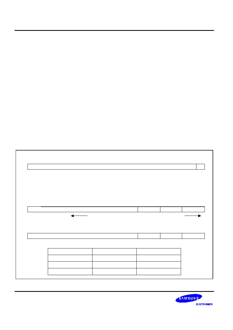
SYSTEM CONFIGURATION
S3C2501X
4-6
AHB Bus Programmable Priority Registers are HPRIF(Programmable Priority Register for Fixed) and HPRIR
(Programmable Priority Register for Round-Robin).
If system configuration register (0xF0000000) SYSCFG[0] = 0x1, the programmable fixed priority is run by
HPRIF register. Each master has its own fixed priority index. For example, GDMA has the index 0. The index for
each master is shown in Figure 4-4. The reset value of HPRIF register is 0x00543210. The first field of
HPRIF[3:0] indicates the highest priority and the HPRIF[7:4] indicates the second highest priority and so on.
HPRIF[23:12] should not be writtern any value and must always be 0x543.
The users are allowed to program HPRIF[11:0]. When the SYSCFG[0] = 0x1 and the HPRIF is 0x00543012, the
fixed priority order form the highest to the lowest is Ethernet controller1, ethernet controller0 and General DMA.
If system configuration register (0xF0000000) SYSCFG[0] = 0x0, the programmable round-robin priority is run by
HPRIR register. All AHB bus masters own their respective field position in HPRIR. The ratio of the bus occupancy
can be programmed by writing an arbitrary value on each field. The arbitrary value can be 0x0 to 0xF.
The reset value of HPRIR register is 0x00000000. The position for each master is shown in Figure 4-4.
The ratio of the bus occupancy of the bus master in the first field is intended to be
(hprir0+1)/((hprir2+1)+(hprir1+1)+(hprir0+1)+3) and so on. However, the arbiter of S3C2501X has a fairness
problem.
The HPRIR should be programmed by the value of 0x000330 to have the same occupancy ratio for three
masters.
The arbiter has a problem that the GDMA always has three more chances to occupy the bus than other masters.
Therefore, hprir2 and hprir1 should have the value of (hprir0+3) to keep the same occupancy ratio.
HPRIR
12 11
8
7
4
3
0
hprir0
hprir1
hprir2
31
Reserved
High Priority
Low Priority
HPRIF
12 11
8
7
4
3
0
hprif0
hprif1
hprif2
31
Reserved
AHB Masters
Index for HPRIF
Field for HPRIR
General DMA (GDMA)
0
HPRIR[3:0]
Ethernet Contoller 0
1
HPRIr[7:4]
Ethernet Contoller 1
2
HPRIR[11:8]
x
0
1
31
[0] System bus arbitration method (ARB)
0 = Round-robin
1 = Fixed priority
SYSCFG
NOTE:
See page 4-16 and 4-17.
Figure 4-4. AHB Programmable Priority Registers

S3C2501X
SYSTEM CONFIGURATION
4-7
4.6.1 PROBLEM SOLVINGS WITH PROGRAMMABLE ROUND-ROBIN
S3C2501X has a stuff to think about with arbiter operation. This only applies to arbiter with Round-Robin priority.
Assuming all '0's are set for HPRIR register for Round-Robin, HPRIR (all same bus occupancy in Round-Robin),
and only three of six masters are used, the problem arises as follows.
Number
HPRIR
Channel
Expected Bus
Occupancy
Actual Running
Block
Real System
Bus Occupancy
1
0
GDMA
1/3
GDMA
1/6
2
0
Ethernet Controller 0
1/3
Ethernet Controller 0
1/6
3
0
Ethernet Controller 1
1/3
Ethernet Controller 1
1/6
4
0
Reserved Master 0
0
GDMA
1/6
5
0
Reserved Master 1
0
GDMA
1/6
6
0
Reserved Master 2
0
GDMA
1/6
When HPRIR is 0x0 and only GDMA , Ethernet controller 0 and 1 are used, the expected bus occupancy for each
channel is 1/3. However, S3C2501X does not work that way, instead, GDMA gets 4/6 of the bus occupancy,
Ethernet controller 0 1/6, and Ethernet controller 1 1/6. In short, GDMA is run four times more than Ethernet
controller 0 and 1. This is because S3C2501X is designed to turn the bus occupancy to the next master when
there is non-used master. For instance,
Number 1: GDMA
Number 2: Ethernet controller 0
Number 3: Ethernet controller 1
Number 4: Reserved Master 0
go to number 5: Reserved Master 1
go to number 6: Reserved Master 2
go to number 1: GDMA
Number 5: Reserved Master 1
go to number 6: Reserved Master 2
go to number 1: GDMA
Number 6: Reserved Master 2
go to number 1: GDMA

SYSTEM CONFIGURATION
S3C2501X
4-8
The following is the problem solving with software.
HPRIR
Channel
Expected
Bus
Occupancy
Real
System Bus
Occupancy
HPRIR
Channel
Occupancy
0
GDMA
1/3
4/6
0
GDMA
1/3
0
Ethernet
controller 0
1/3
1/6
3
Ethernet
controller 0
1/3
0
Ethernet
controller 1
1/3
1/6
3
Ethernet
controller 1
1/3
0
0
0
0
0
0
0
0
0
0
0
0
0
0
0
Problem
Problem Solving
Writing "0x000330", instead of "0x0" will give each channel of three masters with the same amount of bus
occupancy. This is because GDMA is run to fill the blank of reserved masters.

S3C2501X
SYSTEM CONFIGURATION
4-9
4.7 CLOCK CONFIGURATION
The S3C2501X has three PLL clocking scheme ≠ CPU PLL, System BUS PLL, PHY PLL. All of the PLL can
operate if the corresponding clock select pin is set to "0" (CLKSEL- shared with CPU PLL and System BUS PLL,
PHY_CLKSEL). When the clock select pin is set to "1", the PLL goes into power down state. The CPU PLL can
generate ARM940T clock or system bus clock depending on clock mode selection (CLKMOD[1:0]). The System
BUS PLL generates system bus clock only. The PHY PLL generates clock for external devices. Each PLL clock
output frequency can be programmed by either the pin setting or software setting. In pin configurable mode, the
CPU_FREQ[2:0] pins determine the frequency of the CPU PLL clock output and the BUS_FREQ[2:0] pins
determine the frequency of the System BUS PLL clock output. The PHY_FREQ pin determines the frequency of
the PHY PLL output. The PHY PLL generates 2 times the input clock if the PHY_FREQ is "0" and 2.5 times the
input clock if the PHY_FREQ is "1".
The CLKMOD[1:0] pins determine the relation of the ARM940T clock and the system clock. If the CLKMOD[1:0]
is "00", the fastbus clock mode is defined. In this mode, the ARM940T clock and the system bus clock is the
same clock and the clock is from the CPU PLL output. The two clocks are of the same phase and of the same
frequency. If the CLKMOD[1:0] is "10" or "01", the sync clock mode is defined. In this mode, the frequency of the
ARM940T clock is always 2 times that of the system bus clock. If the CLKMOD[1:0] is "11", the async clock mode
is defined. In this mode, the ARM940T clock is out of the CPU PLL and the system bus clock is out of the System
BUS PLL. The frequency of the two clocks could be set to any frequency so long as the the frequency of the
ARM940T clock is faster than that of the system bus clock. The table 4-3 shows the clock configuration of the
external pin setting.
Table 4-3. Clock Frequencies for CLKMOD Pins, CPU_FREQ Pins, and BUS_FREQ Pins
CLKMOD [1:0]
CPU_FREQ [2:0]
BUS_FREQ [2:0]
ARM940T Clock
Frequency
AMBA BUS Clock
Frequency
2'b00 (Fastbus)
3'b000
3'bxxx
166MHz
166MHz
3'b001
3'bxxx
150MHz
150MHz
3'b010
3'bxxx
133MHz
133MHz
3'b011
3'bxxx
125MHz
125MHz
3'b100
3'bxxx
100MHz
100MHz
3'b101
3'bxxx
66MHz
166MHz
3'b110
3'bxxx
50MHz
50MHz
3'b111
3'bxxx
33MHz
33MHz
2'b10 (Sync1)
3'b000
3'bxxx
166MHz
83MHz
3'b001
3'bxxx
150MHz
75MHz
3'b010
3'bxxx
133MHz
66MHz
3'b011
3'bxxx
125MHz
62.5MHz
3'b100
3'bxxx
100MHz
50MHz
3'b101
3'bxxx
66MHz
33MHz
3'b110
3'bxxx
50MHz
25MHz

SYSTEM CONFIGURATION
S3C2501X
4-10
Table 4-3. Clock Frequencies for CLKMOD Pins, CPU_FREQ Pins, and BUS_FREQ Pins (Continued)
CLKMOD [1:0]
CPU_FREQ [2:0]
BUS_FREQ [2:0]
ARM940T Clock
Frequency
AMBA BUS Clock
Frequency
2'b10 (Sync1)
3'b111
3'bxxx
33MHz
16.5MHz
2'b01 (Sync0)
3'b000
3'bxxx
300MHz
150MHz
3'b001
3'bxxx
266MHz
133MHz
3'b010
3'bxxx
233MHz
116.5MHz
3'b011
3'bxxx
200MHz
100MHz
3'b100
3'bxxx
166MHz
83MHz
3'b101
3'bxxx
166MHz
83MHz
3'b110
3'bxxx
166MHz
83MHz
3'b111
3'bxxx
166MHz
83MHz
2'b11 (Async)
3'b000
3'b000
166MHz
133MHz
3'b000
3'b001
166MHz
133MHz
3'b000
3'b010
166MHz
133MHz
3'b000
3'b011
166MHz
125MHz
3'b000
3'b100
166MHz
100MHz
3'b000
3'b101
166MHz
66MHz
3'b000
3'b110
166MHz
50MHz
3'b000
3'b111
166MHz
33MHz
2'b11 (Async)
3'b001
3'b000
150MHz
133MHz
3'b001
3'b001
150MHz
133MHz
3'b001
3'b010
150MHz
133MHz
3'b001
3'b011
150MHz
125MHz
3'b001
3'b100
150MHz
100MHz
3'b001
3'b101
150MHz
66MHz
3'b001
3'b110
150MHz
50MHz
3'b001
3'b111
150MHz
33MHz
Not supported

S3C2501X
SYSTEM CONFIGURATION
4-11
Table 4-3. Clock Frequencies for CLKMOD Pins, CPU_FREQ Pins, and BUS_FREQ Pins (Continued)
CLKMOD [1:0]
CPU_FREQ [2:0]
BUS_FREQ [2:0]
ARM940T Clock
Frequency
AMBA BUS Clock
Frequency
2'b11(Async)
3'b010
3'b000
133MHz
133MHz
3'b010
3'b001
133MHz
133MHz
3'b010
3'b010
133MHz
133MHz
3'b010
3'b011
133MHz
125MHz
3'b010
3'b100
133MHz
100MHz
3'b010
3'b101
133MHz
66MHz
3'b010
3'b110
133MHz
50MHz
3'b010
3'b111
133MHz
33MHz
2'b11 (Async)
3'b011
3'b000
125MHz
133MHz
3'b011
3'b001
125MHz
133MHz
3'b011
3'b010
125MHz
133MHz
3'b011
3'b011
125MHz
125MHz
3'b011
3'b100
125MHz
100MHz
3'b011
3'b101
125MHz
66MHz
3'b011
3'b110
125MHz
50MHz
3'b011
3'b111
125MHz
33MHz
2'b11 (Async)
3'b100
3'b000
100MHz
133MHz
3'b100
3'b001
100MHz
133MHz
3'b100
3'b010
100MHz
133MHz
3'b100
3'b011
100MHz
125MHz
3'b100
3'b100
100MHz
100MHz
3'b100
3'b101
100MHz
66MHz
3'b100
3'b110
100MHz
50MHz
3'b100
3'b111
100MHz
33MHz
2'b11 (Async)
3'b101
3'b000
66MHz
133MHz
3'b101
3'b001
66MHz
133MHz
3'b101
3'b010
66MHz
133MHz
3'b101
3'b011
66MHz
125MHz
3'b101
3'b100
66MHz
100MHz
3'b101
3'b101
66MHz
66MHz
3'b101
3'b110
66MHz
50MHz
3'b101
3'b111
66MHz
33MHz
Not supported

SYSTEM CONFIGURATION
S3C2501X
4-12
Table 4-3. Clock Frequencies for CLKMOD Pins, CPU_FREQ Pins, and BUS_FREQ Pins (Continued)
CLKMOD [1:0]
CPU_FREQ [2:0]
BUS_FREQ [2:0]
ARM940T Clock
Frequency
AMBA BUS Clock
Frequency
2'b11 (Async)
3'b110
3'b000
50MHz
133MHz
3'b110
3'b001
50MHz
133MHz
3'b110
3'b010
50MHz
133MHz
3'b110
3'b011
50MHz
125MHz
3'b110
3'b100
50MHz
100MHz
3'b110
3'b101
50MHz
66MHz
3'b110
3'b110
50MHz
50MHz
3'b110
3'b111
50MHz
33MHz
Not supported
Each PLL can also be programmed by S/W register setting. Each PLL is in pin configurable mode after the
system reset is released. You can change the PLL configuration mode to the register configurable mode by set
CPLLREN, SPLLREN, PPLLREN in the SYSCFG[31:28]. If the PLL register enable bit is set to "1, the PLL
multiplication factor is not from the external pin but from the corresponding PLLCON regiseter-CPLLCON,
SPLLCON, PPLLCON registers. The PLL is controlled by the 3 control variables, P, M ,S. When the PLL is under
the control of the S/W and the PLL control variables are dynamically changed by the S/W, the glitch may occur in
the PLL output clock. You can avoid the glitch generation by set the PLL clock enable bit, CPLLCE, SPLLCE,
PPLLCE in the SYSCFG [27:24]. When the PLL clock enable bit is set to "0" during the PLL control variable
change, the stable PLL output clock is provided. The PLL output frequency is determined as follows.
Fout = Fin
◊
(M+8) / ((P+2)
◊
(2^S))
Where the Fin is the frequency of the PLL input clock and the Fout is the frequency of the PLL output clock.
The four PLLs in the S3C2501X are controlled by above formula and the table 4-4 shows the PLL variables for
the most widely used frequencies.

S3C2501X
SYSTEM CONFIGURATION
4-13
Table 4-4. P, M, S values of the S3C2501X PLL
P[5:0]
M[7:0]
S[1:0]
PLL Input Clock
Frequency
PLL Output Clock
Frequency
00_0001
0101_0010
00
10MHz
300MHz
00_0001
0100_1000
00
10MHz
266MHz
00_0001
1000_0100
01
10MHz
233MHz
00_0001
0111_0000
01
10MHz
200MHz
00_0011
1001_1110
01
10MHz
166MHz
00_0001
0101_0010
01
10MHz
150MHz
00_0001
0100_1000
01
10MHz
133MHz
00_0001
0100_0011
01
10MHz
125MHz
00_0001
0111_0000
10
10MHz
100MHz
00_0011
1011_1000
10
10MHz
96MHz
00_0001
0100_1000
10
10MHz
66MHz
00_0001
0111_0000
11
10MHz
50MHz
00_0011
1011_1000
11
10MHz
48MHz
00_0001
0100_1000
11
10MHz
33MHz

SYSTEM CONFIGURATION
S3C2501X
4-14
NOTES:
1. CPU PLL block can generate eight clock frequencies between 166MHz and 33MHz according to the
CPU_FREQ[2:0] pins out of the 10MHz XCLK input clock frequency.
2. If CLKSEL, CPU PLL, or BUS PLL go into the state of power down.
3. Three pins of CPU_FREQ[2:0] can control the multiplication factor of the CPU PLL block.
4. The PHY_FREQ pin controls the frequency of the PHY PLL.
5. The system configuration register CLKCON[15:0] can divide the ARM9 clock and the system clock. If all bits are 0,
non-divided clock is used.Only one bit can be set in CLKCON[15:0]. That is, the clock dividing value is defined as
1, 2, 4, 8, 16, .... The internal clock is (PLL output clock between 166MHz and 33MHz) / (CLKCON+1).
6. The CLKCON[15:0] register, CLKMOD[1:0] pins and CPU_FREQ[2:0] pins can control the AMBA clock divider.
The CLKMOD[1:0] pins and BUS_FREQ[2:0] pins can generate the various AMBA bus clock frequecies referring
to the Table 3. The CLKCON[15:0] register can divide the various AMBA clock frequecies of the Table 4-3.
7. All PLL can be controlled by either pin setting or register setting.
{CLKCON[15:0], CLKMOD[1:0],
BUS_FREQ[2:0]}
CPU PLL
166-33
MHz
0
1
ARM940T
Block
ARM
Clock
Divider
CPU_FREQ[2:0] or
pdown
CLKSEL
CLKCON[15:0]
BUS PLL
Block
AMBA
Divider
BUS_FREQ[2:0] or
pdown
CLKSEL
0
1
1
PLL_TEST
Clock
Divider
pin
PLL_TEST & PP[1:0]
PHY PLL
20/25
0
1
PPLLCON
pdown
XCLK
PHY_CLKO
MHz
Figure 4-5. Shows the Clock Generation Logic of the S3C2501X

S3C2501X
SYSTEM CONFIGURATION
4-15
4.8 SYSTEM CONFIGURATION SPECIAL REGISTERS
The System Configuration reigisters are as follows.
Table 4-5. System Configuration Registers
Name
Address
Description
Reset Value
SYSCFG
0xF0000000
System configuration register
≠
PDCODE
0xF0000004
Product code and revision number register
0x25010000
CLKCON
0xF0000008
System clock control register
0x00000000
PCLKDIS
0xF000000C
Peripheral clock disable register
0x0F000500
CLKST
0xF0000010
Clock Status register
HPRIF
0xF0000014
AHB bus master fixed priority register
0x00543210
HPRIR
0xF0000018
AHB bus master round-robin priority register
0x00000000
CPLLCON
0xF000001C
Core PLL Configuration Register
0x0001039E
SPLLCON
0xF0000020
System BUS PLL Configuration Register
0x00010370
PPLLCON
0xF0000028
PHY PLL Configuration Register
0x000103111

SYSTEM CONFIGURATION
S3C2501X
4-16
4.8.1 SYSTEM CONFIGURATION REGISTER (SYSCFG)
You can control the system bus arbitration method, PLL operation, system clock output enable/disable function,
external memory address remap function and Little/Big information read function by SYSCFG.
Register
Address
R/W
Description
Reset Value
SYSCFG
0xF0000000
R/W
System configuration register
≠
SYSCFG
Bit
Description
Initial State
CPLLREN
[31]
CPLLCON Register Enable
This bit controls which value is used for the CPU PLL constant from
the two constant values. When this bit is set to "0", the CPU PLL
constant is from CPU_FREQ[2:0] setting. When this bit is set to "1",
the CPU PLL constant is from the CPLLCON register.
0
SPLLREN
[30]
SPLLCON Register Enable
This bit controls which value is used for the BUS PLL constant from
the two constant values. When this bit is set to "0", the BUS PLL
constant is from BUS_FREQ[2:0] setting. When this bit is set to "1",
the BUS PLL constant is from the SPLLCON register.
0
PPLLREN
[28]
PPLLCON Register Enable
This bit controls which value is used for the PHY PLL constant from
the two constant values. When this bit is set to "0", the PHY PLL
constant is from PHY_FREQ setting. When this bit is set to "1", the
PHY PLL constant is from the PPLLCON register.
0
CPLLFD
[27]
CPLL Filter Disable
This bit determines whether the CPU PLL output is filtered or not
during the configuration. When this bit is set to "0", the CPU PLL
output is filtered to be provided to the system during the
configuration. In this case, the glitch output from PLL can be
masked. When this bit is set to "1", the CPU PLL output is not
filtered to be provided to the system.
0
SPLLFD
[26]
SPLL Filter Disable
This bit determines whether the BUS PLL output is filtered or not
during the configuration. When this bit is set to "0", the BUS PLL
output is filtered to be provided to the system during the
configuration. In this case, the glitch output from PLL can be
masked. When this bit is set to "1", the BUS PLL output is not
filtered to be provided to the system.
0

S3C2501X
SYSTEM CONFIGURATION
4-17
SYSCFG
Bit
Description
Initial State
PPLLFD
[24]
PPLL Filter Disable
This bit determines whether the PHY PLL output is filtered or not
during the configuration. When this bit is set to "0", the PHY PLL
output is filtered to be provided to the PHY during the configuration.
In this case, the glitch output from PLL can be masked. When this
bit is set to "1", the PHY PLL output is not filtered to be provided to
the PHY.
0
BIG
[16]
Little / Big endian information (Read only)
0 = Little endian 1 = Big endian
≠
REMAP
[8]
External memory address remapping enable
0 = Remap disable 1 = Remap Enable
ROM Bank0 : 0x00000000 ROM Bank0 : 0x80000000
ROM Bank1 : 0x01000000 ROM Bank1 : 0x81000000
ROM Bank2 : 0x02000000 ROM Bank2 : 0x82000000
ROM Bank3 : 0x03000000 ROM Bank3 : 0x83000000
ROM Bank4 : 0x04000000 ROM Bank4 : 0x84000000
ROM Bank5 : 0x05000000 ROM Bank5 : 0x85000000
ROM Bank6 : 0x06000000 ROM Bank6 : 0x86000000
ROM Bank7 : 0x07000000 ROM Bank7 : 0x87000000
SDRAM Bank0 : 0x40000000 SDRAM0 bank0 : 0x00000000
SDRAM Bank1 : 0x80000000 SDRAM1 bank1 : 0x40000000
0
HCLKO_DIS
[4]
HCLKO output disable
If this bit is set to "1", HCLKO output is activated only when sdram
access - sdram read/write or refresh - is enabled. If this bit is set to
"0", HCLKO is always activated.
0 = Enabled always 1 = Enabled during sdram access.
0
ARB
[0]
System bus arbitration method
0 = Round-robin 1 = Fixed priority
0

SYSTEM CONFIGURATION
S3C2501X
4-18
4.8.2 PRODUCT CODE AND REVISION NUMBER REGISTER (PDCODE)
Register
Address
R/W
Description
Reset Value
PDCODE
0xF0000004
R
Product code and revision number register
0x25010000
PDCODE
Bit
Description
Initial State
PC
[31-16]
Product code
0x2501
Reserved
[15:8]
Reserved
0x0
MajRev
[7:4]
Major revision number
0x0
MinRev
[3:0]
Minor revision number
0x0

S3C2501X
SYSTEM CONFIGURATION
4-19
4.8.3 CLOCK CONTROL REGISTER (CLKCON)
There is clock control register(CLKCON) in system configuration. For the purpose of power save, Clock control
register(CLKCON) can be programmed at low frequency and the slower clock than the system clock can be made
by clock dividing value. When the internal system clock is divided by CLKCON, its duty-cycle is changed. If
CLKCON is programmed to zero, the internal system clock remains the same as the internal clock. In other case,
the duty cycle of internal system clock is no logner 50%.
Register
Address
R/W
Description
Reset Value
CLKCON
0xF0000008
R/W
Clock control register
0x00000000
CLKCON
Bit
Description
Initial State
Reserved
[31:16]
Reserved
0
DVAL
[15:0]
System clock dividing value.
If all bits are 0, non-divided clock is used.
Only one bit can be set in CLKCON[15:0]. That is, the clock dividing
value is defined as 1, 2, 4, 8, 16, ...
Internal system clock is (PLL output clock) / (CLKCON+1).
0
HCLK
HCLK
CLKCON = 0
HCLK
CLKCON = 1
HCLK
CLKCON = 2
Figure 4-6. Divided System Clock Timing Diagram

SYSTEM CONFIGURATION
S3C2501X
4-20
4.8.4 PERIPHERAL CLOCK DISABLE REGISTER (PCLKDIS)
There is a peripheral clock disable register in system configuration. You can set this register with the specific
value for the purpose of power save. If you set PCLKDIS[0] to "1", the clock for GDMA channel 0 is
disabled. Similarly, you control the clock input of each peripheral.
Register
Address
R/W
Description
Reset Value
PCLKDIS
0xF000000C
R/W
Peripheral clock disable register
0x0F000500
PCLKDIS
Bit
Description
Initial State
SRreq
[31]
SDRAM Self-refresh request
0x0
SRack
[30]
SDRAM Self-refresh acknowledge ( Read only)
0x0
Reserved
[29:28]
Reserved for future use
0x0
Reserved
[27]
Reserved
1
Reserved
[26]
Reserved
1
Reserved
[25]
Reserved
1
Reserved
[24]
Reserved
1
SDRAMC
[23]
SDRAMC clock disable
0x0
MEMCON
[22]
MEMCON clock disable
0x0
DES
[21]
DES clock disable
0x0
IIC
[20]
IIC Clock disable
0x0
IOPC
[19]
IOPC clock disable
0x0
WDT
[18]
Watch dog timer clock disable
0x0
TIMER5
[17]
TIMER5 clock disable
0x0
TIMER4
[16]
TIMER4 clock disable
0x0
TIMER3
[15]
TIMER3 clock disable
0x0
TIMER2
[14]
TIMER2 clock disable
0x0
TIMER1
[13]
TIMER1 clock disable
0x0
TIMER0
[12]
TIMER0 clock disable
0x0
HUART
[11]
HUART clock disable
0x0
Reserved
[10]
Reserved
1
CUART
[9]
CUART clock disable
0x0
Reserved
[8]
Reserved
1
ETHERC1
[7]
ETHERC1 clock disable
0x0
ETHERC0
[6]
ETHERC0 clock disable
0x0
GDMA5
[5]
GDMA channel 5 clock disable
0x0
GDMA4
[4]
GDMA channel 4 clock disable
0x0
GDMA3
[3]
GDMA channel 3 clock disable
0x0
GDMA2
[2]
GDMA channel 2 clock disable
0x0
GDMA1
[1]
GDMA channel 1 clock disable
0x0
GDMA0
[0]
GDMA channel 0 clock disable
0x0

S3C2501X
SYSTEM CONFIGURATION
4-21
4.8.5 CLOCK STATUS REGISTER (CLKST)
The operating frequency of the S3C2501X can be obtained by reading the CLKST register. The CPU Freq field in
CLKST[11:0] decodes the CPU_FREQ[2:0] settings and the BUS Freq in CLKST[23:12] decodes the
BUS_FREQ[2:0] settings. There are 3 clock modes in the S3C2501X - fast mode, sync mode and async mode. In
async mode, there is no misinformation about the frequency. But Care must be taken for the fastbus mode and
sync mode. In the fastbus mode, the BUS frequency in the CLKST[23:12] should be ignored and the CPU
frequency in the CLKST[11:0] should be taken for the BUS frequency because the CPU clock and system bus
clock is the same. In the sync mode, the BUS frequency in the CLKST[23:12] should also be ignored , and the
half of the CPU frequency should be taken for the BUS frequency.
Register
Address
R/W
Description
Reset Value
CLKST
0xF0000010
R
Clock Status register (Read Only)
≠
CLKST
Bit
Description
Initial State
Clock Mode
[31:30]
00 = FastBus mode
10 = Reserved
01 = Synchronous
11 = Asynchronous
Reserved
[29:24]
BUS Freq
[23:12]
System Bus Clock frequency
CPU Freq
[11:0]
CPU Clock frequency
4.8.6 AHB BUS MASTER PRIORITY REGISTER
Register
Address
R/W
Description
Reset Value
HPRIF
0xF0000014
R/W
AHB bus master fixed priority register
0x00543210
HPRIR
0xF0000018
R/W
AHB bus master round-robin priority register
0x00000000

SYSTEM CONFIGURATION
S3C2501X
4-22
4.8.7 CORE PLL CONTROL REGISTER (CPLLCON)
If you want to use this register, you should set CPLLREN in SYSCFG[31] to "1". This register doesn't work with
CPLLREN set to "0".
Register
Address
R/W
Description
Reset Value
CPLLCON
0xF000001C
R/W
Core PLL control register
0x0001039E
CPLLCON
Bit
Description
Initial State
Reserved
[31:12]
0x0
S
[17:16]
Scaler
0x1
Reserved
[15:14]
0x0
P
[13:8]
Pre divider
0x3
M
[7:0]
Main divider
0x9E
Output clock frequency is determined by following formula.
Fout = Fin
◊
(M+8) / ((P+2)
◊
(2^S))
If Fin = 10MHz, P = 3, M = 158 (0x9E), and S = 1, Fout is 166 MHz.
FCLK signal of ARM940T core is connected to Fout, 166MHz clock. But, BCLK signal of ARM940T and system
bus clock is connect to Fout / 2, 66 MHz clock.

S3C2501X
SYSTEM CONFIGURATION
4-23
4.8.8 SYSTEM BUS PLL CONTROL REGISTER (SPLLCON)
If you want to use this register, you should set SPLLREN in SYSCFG[30] to "1". This register doesn't work with
SPLLREN set to "0".
Register
Address
R/W
Description
Reset Value
SPLLCON
0xF0000020
R/W
System BUS PLL control register
0x0001037D
SPLLCON
Bit
Description
Initial State
Reserved
[31:12]
0x0
S
[17:16]
Scaler
0x1
Reserved
[15:14]
0x0
P
[13:8]
Pre divider
0x3
M
[7:0]
Main divider
0x7D
Output clock frequency is determined by following formula.
Fout = Fin
◊
(M+8) / ((P+2)
◊
(2^S))
If Fin = 10MHz, P = 3, M = 125 (0x7D), and S = 1, Fout is 133 MHz.
FCLK signal of ARM940T core is connected to Fout, 133MHz clock. But, BCLK signal of ARM940T and system
bus clock is connect to Fout / 2, 66 MHz clock.

SYSTEM CONFIGURATION
S3C2501X
4-24
4.8.9 PHY PLL CONTROL REGISTER (PPLLCON)
If you want to use this register, you should set PPLLREN in SYSCFG[28] to "1". This register doesn't work with
PPLLREN set to "0".
Register
Address
R/W
Description
Reset Value
PPLLCON
0xF0000028
R/W
PHY PLL control register
0x00010311
PPLLCON
Bit
Description
Initial State
Reserved
[31:12]
0x0
S
[17:16]
Scaler
0x1
Reserved
[15:14]
0x0
P
[13:8]
Pre divider
0x3
M
[7:0]
Main divider
0x11
Output clock frequency is determined by following formula.
Fout = Fin
◊
(M+8) / ((P+2) * (2^S))
If Fin = 10MHz, P = 3, M = 17 (0x11), and S = 1, Fout is 25MHz.

S3C2501X
MEMORY CONTROLLER
5-1
5
MEMORY CONTROLLER
5.1 OVERVIEW
This Memory controller consists of Ext I/O Bank controller and SDRAM controller. Ext I/O Bank controller
supports ROM, SRAM and Flash memory. SDRAM controller support SDRAM.
The S3C2501X Memory controller has the following functions.
∑
To provide the required memory control signals for external memory accesses. For example, if a master
block such as DMA controller or CPU generates an address that corresponds to a SDRAM bank, the SDRAM
controller generates the required SDRAM access signals.
∑
To provide the required signals for bus traffic between the S3C2501X and ROM/SRAM and the external
I/O banks.
∑
∑
To compensate for differences in bus width for data flowing between the external memory bus and the
internal data bus.
∑
S3C2501X supports both little and big endians for external memory or I/O devices.

MEMORY CONTROLLER
S3C2501X
5-2
5.2 FEATURES
The following is a list of the Memory Controller's features:
∑
10 banks (8 banks for ROM / SRAM / Flash Memory / External I/O interface, 2 banks for SDRAM interface )
∑
16M-byte maximum address range per bank (24 bit external address pins)
∑
32 bit internal and external data bus
∑
Various timing control options
NOTE
By generating an external bus request, an external device can access the S3C2501X's external memory
interface pins. In addition, the S3C2501X can access slow external devices by using a WAIT signal. The
WAIT signal, which is generated by the external device, extends the duration of the CPU's memory
access cycle beyond its programmable value.
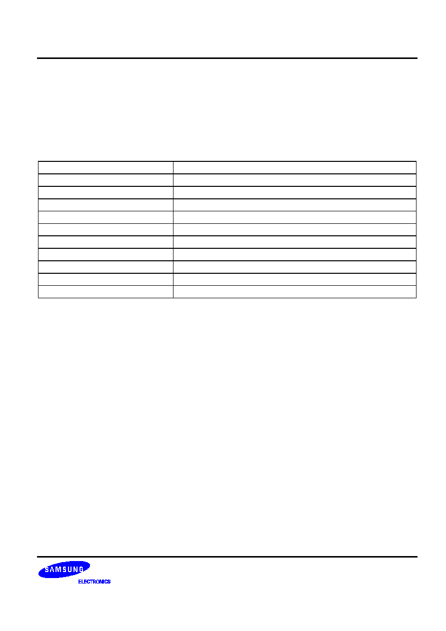
S3C2501X
MEMORY CONTROLLER
5-3
5.3 MEMORY MAP
After a power-on or system reset, all bank address pointer registers are initialized to their default values. And the
base address of all banks are fixed.
The initial system memory map following system start-up is shown in Figure 5-1.
Table 5-1. Base Address of Each Bank
Bank
Base Address
EXT I/O Bank 0
0x00000000
EXT I/O Bank 1
0x01000000
EXT I/O Bank 2
0x02000000
EXT I/O Bank 3
0x03000000
EXT I/O Bank 4
0x04000000
EXT I/O Bank 5
0x05000000
EXT I/O Bank 6
0x06000000
EXT I/O Bank 7
0x07000000
SDRAM Bank 0
0x40000000
SDRAM Bank 1
0x80000000

MEMORY CONTROLLER
S3C2501X
5-4
,
0xFFFFFFFF
0xF0000000
0x88000000
0x80000000
0x40000000
0x08000000
0x07000000
0x06000000
0x05000000
0x04000000
0x03000000
0x02000000
0x01000000
0x00000000
Reserved
Internal Register
Bank 1
Reserved
Reserved
EXT I/O Bank 7
EXT I/O Bank 6
EXT I/O Bank 5
EXT I/O Bank 4
EXT I/O Bank 3
EXT I/O Bank 1
EXT I/O Bank 2
EXT I/O Bank 0
NOTES:
1. ROM, SRAM, Flash and External I/O Bank have the same operation in internal logic.
Therefore you may connect a SRAM or a Flash Memory with a External I/O Bank.
2. Each EXT I/O bank address is fixed with maximum address range.
S3C2501X has 24 address pins, which restrict to 16M-byte address.
3. Each SDRAM bank supports up to 128M-byte in size.
Bank 0
0x48000000
Figure 5-1. Memory Bank Address map

S3C2501X
MEMORY CONTROLLER
5-5
5.4 BUS INTERFACE SIGNALS
The bus interface signals transfer information between the S3C2501X and external memory device.
These divide into address and data which used commonly, SDRAM interface signals for SDRAM and memory
device interface for ROM/SRAM, etc.
For detail description for the bus interface signals, refer to the table below.
Table 5-2. Bus Interface Signals
Signal Name
Pins
Active
I/O
Description
ADDR
24
HIGH
O
Specifies the physical address of the external device
DATA
32
HIGH
B
Specifies data of the external device
B0SIZE
2
HIGH
I
Specifies data bus access size for the Bank 0
nOE
1
LOW
O
Specifies read/write state from S3C2501X. When
S3C2501X read from ext I/O device, nOE's value is
1'b0.
nRCS
8
LOW
O
Specifies which ext I/O device is selected.
nEWAIT/nREADY
1
LOW
I
Signal be controlled from ext I/O slow device to delay
cycles in data read and write.
HCLKO
1
HIGH
O
S3C2501X system clock out
CKE
1
HIGH
O
Clock enable for SDRAM
nSDCS
2
LOW
O
Chip select strobe for SDRAM
nSDRAS
1
LOW
O
Row address strobe for SDRAM
nSDCAS
1
LOW
O
Column address strobe for SDRAM
nWBE/nBE/DQM
4
LOW
O
Write byte enable
nSDWE/nWE16
1
LOW
O
Write enable for ROM, SRAM, Flash that have 16bit-
data width and SDRAM.
XBMREQ
1
HIGH
I
External Master bus request
XBMACK
1
HIGH
O
External bus acknowledge
NOTES:
1. O = Output from the S3C2501X.
2. I = Input to the S3C2501X.
3. B = Bi-direction.

MEMORY CONTROLLER
S3C2501X
5-6
Address & Data
ROM & SRAM
Interface signals
SDRAM Interface
signals
ROM, SRAM, Flash
and SDRAM common
signals
External device
interface signals
Adjust with pin
selection
nOE
nRCS[7:0]
ADDR[23:0]
HCLKO
CKE
nSDCS[1:0]
nSDRAS
nSDCAS
nWBE/nBE/DQM[3:0]
nEWAIT/nREADY
nSDWE/nWE16
B0SIZE[1:0]
XBMREQ
DATA[31:0]
XBMACK
S3C2501X
Figure 5-2. Memory Controller Bus Signals

S3C2501X
MEMORY CONTROLLER
5-7
5.5 ENDIAN MODES
S3C2501X supports both little-endian and big-endian for external memory or I/O devices by setting the pin BIG.
Below tables(5-3 through 5-14) are show the program/data path between the CPU register and the external
memory using little-/big-endian and word/half-word/byte access.
Table 5-3 and 5-4.
Using big-endian and word access, Program/Data path between register and external memory.
WA=Address whose LSB is 0, 4, 8, C, HA=Address whose LSB is 0, 2, 4, 6, 8, A, C, E
BA=Address whose LSB is 0, 1, 2, 3, 4, 5, 6, 7, 8, 9, A, B, C, D, E, F
EA=External Address X=Don't care
Table 5-3. External 32-bit Datawidth Store Operation with Big-Endian
Transfer Width
STORE (CPU Reg
External Memory)
32-bit
16-bit
8-bit
Bit Num.
CPU Register Data
31 0
abcd
31 0
xxab
31 0
xxcd
31 0
xxxa
31 0
xxxb
31 0
xxxc
31 0
xxxd
CPU Address
WA
HA
HA+1
BA
BA+1
BA+2
BA+3
Bit Num.
CPU Data Bus
31 0
abcd
31 0
abab
31 0
cdcd
31 0
aaaa
31 0
bbbb
31 0
cccc
31 0
dddd
External Address (ADDR)
EA
Bit Num.
External DATA
31 0
dcba
31 0
xxba
31 0
dcxx
31 0
xxxa
31 0
xxbx
31 0
xcxx
31 0
dxxx
Timing Sequence
Table 5-4. External 32-bit Datawidth Load Operation with Big-Endian
Transfer Width
LOAD (CPU Reg
External Memory)
32-bit
16-bit
8-bit
Bit Num.
CPU Register Data
31 0
abcd
31 0
xxab
31 0
xxcd
31 0
xxxa
31 0
xxxb
31 0
xxxc
31 0
xxxd
CPU Address
WA
HA
HA+1
BA
BA+1
BA+2
BA+3
Bit Num.
CPU Data Bus
31 0
abcd
31 0
abab
31 0
cdcd
31 0
aaaa
31 0
bbbb
31 0
cccc
31 0
dddd
External Address (ADDR)
EA
Bit Num.
External DATA
31 0
dcba
31 0
dcba
31 0
dcba
Timing Sequence

MEMORY CONTROLLER
S3C2501X
5-8
Table 5-5 and 5-6.
Using big-endian and half-word access, Program/Data path between register and external memory.
WA=Address whose LSB is 0, 4, 8, C, EA=External Address
HA=Address whose LSB is 0, 2, 4, 6, 8, A, C, E
BA=Address whose LSB is 0, 1, 2, 3, 4, 5, 6, 7, 8, 9, A, B, C, D, E, F
X=Don't care.
Table 5-5. External 16-bit Datawidth Store Operation with Big-Endian
Transfer Width
STORE (CPU Reg
External Memory)
32-bit
16-bit
8-bit
Bit Num.
CPU Register Data
31 0
abcd
31 0
xxab
31 0
xxxa
31 0
xxxb
CPU Address
WA
HA
BA
BA+1
Bit Num.
CPU Data Bus
31 0
abcd
31 0
abab
31 0
aaaa
31 0
bbbb
External Address (ADDR)
EA
EA+1
EA
EA
Bit Num.
External DATA
15 0
ba
15 0
dc
15 0
ba
15 0
xa
15 0
bx
Timing Sequence
1st
2nd
Table 5-6. External 16-bit Datawidth Load Operation with Big-Endian
Transfer Width
LOAD (CPU Reg
External Memory)
32-bit
16-bit
8-bit
Bit Num.
CPU Register Data
31 0
abcd
31 0
xxab
31 0
xxxa
31 0
xxxb
CPU Address
WA
HA
BA
BA+1
Bit Num.
CPU Data Bus
31 0
abxx
31 0
abcd
31 0
abab
31 0
aaaa
31 0
bbbb
External Address (ADDR)
EA
EA + 1
EA
EA
Bit Num.
External DATA
15 0
ba
15 0
dc
15 0
ba
15 0
ba
Timing Sequence
1st
2nd

S3C2501X
MEMORY CONTROLLER
5-9
Table 5-7 and 5-8.
Using big-endian and byte access, Program/Data path between register and external memory.
WA=Address whose LSB is 0, 4, 8, C, EA=External Address
HA=Address whose LSB is 0, 2, 4, 6, 8, A, C, E
BA=Address whose LSB is 0, 1, 2, 3, 4, 5, 6, 7, 8, 9, A, B, C, D, E, F
X=Don't care.
Table 5-7. External 8-bit Datawidth Store Operation with Big-Endian
Transfer Width
STORE (CPU Reg
External Memory)
32-bit
16-bit
8-bit
Bit Num.
CPU Register Data
31 0
abcd
15 0
xxab
7 0
xxxa
CPU Address
WA
HA
BA
Bit Num.
CPU Data Bus
31 0
abcd
31 0
abab
31 0
aaaa
External Address
EA
EA+1
EA+2
EA+3
EA
EA+1
EA
Bit Num.
External DATA
7 0
a
7 0
b
7 0
c
7 0
d
7 0
a
7 0
b
7 0
a
Timing Sequence
1st
2nd
3rd
4th
1st
2nd
Table 5-8. External 8-bit Datawidth Load Operation with Big-Endian
Transfer Width
LOAD (CPU Reg
External Memory)
32-bit
16-bit
8-bit
Bit Num.
CPU Register Data
31 0
abcd
15 0
xxab
7 0
xxxa
CPU Address
WA
HA
BA
Bit Num.
CPU Data Bus
31 0
axxxx
31 0
abxx
31 0
abcx
31 0
abcd
31 0
axax
31 0
abab
31 0
aaaa
External Address
EA
EA+1
EA+2
EA+3
EA
EA+1
EA
Bit Num.
External DATA
7 0
a
7 0
b
7 0
c
7 0
d
7 0
a
7 0
b
7 0
a
Timing Sequence
1st
2nd
3rd
4th
1st
2nd

MEMORY CONTROLLER
S3C2501X
5-10
Table 5-9 and 5-10.
Using little-endian and word access, Program/Data path between register and external memory.
WA=Address whose LSB is 0, 4, 8, C, EA=External Address
HA=Address whose LSB is 0, 2, 4, 6, 8, A, C, E
BA=Address whose LSB is 0, 1, 2, 3, 4, 5, 6, 7, 8, 9, A, B, C, D, E, F
X=Don't care
Table 5-9. External 32-bit Datawidth Store Operation with Little-Endian
Transfer Width
STORE (CPU Reg
External Memory)
32-bit
16-bit
8-bit
Bit Num.
CPU Register Data
31 0
abcd
31 0
xxcd
31 0
xxab
31 0
xxxd
31 0
xxxc
31 0
xxxb
31 0
xxxa
CPU Address
WA
HA
HA+1
BA
BA+1
BA+2
BA+3
Bit Num.
CPU Data Bus
31 0
abcd
31 0
cdcd
31 0
abab
31 0
dddd
31 0
cccc
31 0
bbbb
31 0
aaaa
External Address (ADDR)
EA
Bit Num.
External DATA
31 0
abcd
31 0
xxcd
31 0
abxx
31 0
xxxd
31 0
xxcx
31 0
xbxx
31 0
axxx
Timing Sequence
Table 5-10. External 32-bit Datawidth Load Operation with Little-Endian
Transfer Width
LOAD (CPU Reg
External Memory)
32-bit
16-bit
8-bit
Bit Num.
CPU Register Data
31 0
abcd
31 0
xxcd
31 0
xxab
31 0
xxxd
31 0
xxxc
31 0
xxxb
31 0
xxxa
CPU Address
WA
HA
HA+1
BA
BA+1
BA+2
BA+3
Bit Num.
CPU Data Bus
31 0
abcd
31 0
cdcd
31 0
abab
31 0
dddd
31 0
cccc
31 0
bbbb
31 0
aaaa
External Address (ADDR)
EA
Bit Num.
External DATA
31 0
abcd
31 0
abcd
31 0
abcd
Timing Sequence

S3C2501X
MEMORY CONTROLLER
5-11
Table 5-11 and 5-12.
Using little-endian and half-word access, Program/Data path between register and external memory.
WA=Address whose LSB is 0, 4, 8, C, EA=External Address
HA=Address whose LSB is 0, 2, 4, 6, 8, A, C, E
BA=Address whose LSB is 0, 1, 2, 3, 4, 5, 6, 7, 8, 9, A, B, C, D, E, F
X=Don't care.
Table 5-11. External 16-bit Datawidth Store Operation with Little-Endian
Transfer Width
STORE (CPU Reg
External Memory)
32-bit
16-bit
8-bit
Bit Num.
CPU Register Data
31 0
abcd
31 0
xxab
31 0
xxxb
31 0
xxxa
CPU Address
WA
HA
BA
BA+1
Bit Num.
CPU Data Bus
31 0
abcd
31 0
abab
31 0
bbbb
31 0
aaaa
External Address (ADDR)
EA+1
EA
EA
EA
Bit Num.
External DATA
15 0
ab
15 0
cd
15 0
ab
15 0
xb
15 0
ax
Timing Sequence
1st
2nd
Table 5-12. External 16-bit Datawidth Load Operation with Little-Endian
Transfer Width
LOAD (CPU Reg
External Memory)
32-bit
16-bit
8-bit
Bit Num.
CPU Register Data
31 0
abcd
31 0
xxab
31 0
xxxb
31 0
xxxa
CPU Address
WA
HA
BA
BA+1
Bit Num.
CPU Data Bus
31 0
abxx
31 0
abcd
31 0
abab
31 0
bbbb
31 0
aaaa
External Address (ADDR)
EA + 1
EA
EA
EA
Bit Num.
External DATA
15 0
ab
15 0
cd
15 0
ab
15 0
ab
Timing Sequence
1st
2nd

MEMORY CONTROLLER
S3C2501X
5-12
Table 5-13 and 5-14.
Using little-endian and byte access, Program/Data path between register and external memory.
WA=Address whose LSB is 0, 4, 8, C, EA=External Address
HA=Address whose LSB is 0, 2, 4, 6, 8, A, C, E
BA=Address whose LSB is 0, 1, 2, 3, 4, 5, 6, 7, 8, 9, A, B, C, D, E, F
X=Don't care.
Table 5-13. External 8-bit Datawidth Store Operation with Little-Endian
Transfer Width
STORE (CPU Reg
External Memory)
32-bit
16-bit
8-bit
Bit Num.
CPU Register Data
31 0
abcd
31 0
xxab
31 0
xxxa
CPU Address
WA
HA
BA
Bit Num.
CPU Data Bus
31 0
abcd
31 0
abab
31 0
aaaa
External Address (ADDR)
EA+3
EA+2
EA+1
EA
EA+1
EA
EA
Bit Num.
External DATA
7 0
a
7 0
b
7 0
c
7 0
d
7 0
a
7 0
b
7 0
a
Timing Sequence
1st
2nd
3rd
4th
1st
2nd
Table 5-14. External 8-bit Datawidth Load Operation with Little-Endian
Transfer Width
LOAD (CPU Reg
External Memory)
32-bit
16-bit
8-bit
Bit Num.
CPU Register Data
31 0
abcd
31 0
xxab
31 0
xxxa
CPU Address
WA
HA
BA
Bit Num.
CPU Data Bus
31 0
axxxx
31 0
abxx
31 0
abcx
31 0
abcd
31 0
axax
31 0
abab
31 0
aaaa
External Address (ADDR)
EA+3
EA+2
EA+1
EA
EA+1
EA
EA
Bit Num.
External DATA
7 0
a
7 0
b
7 0
c
7 0
d
7 0
a
7 0
b
7 0
a
Timing Sequence
1st
2nd
3rd
4th
1st
2nd

S3C2501X
MEMORY CONTROLLER
5-13
5.6 EXT I/O BANK CONTROLLER
Ext I/O Bank controller can be interfaceing ROM, SRAM, flash memory, etc, except SDRAM. It also supports
muxed bus memory device which shares address bus and data bus. Ext I/O bank controller has three kind of the
register for eight banks and then it can be controlled by various timing control options.
5.6.1 FEATURES
The following is a list of the Ext I/O Bank Controller's features:
∑
8 banks
∑
ROM / SRAM / Flash Memory / External I/O interface
∑
16M-byte maximum address range per bank (24-bit external address pins)
∑
32-bit internal and external data bus
∑
Various timing control options

MEMORY CONTROLLER
S3C2501X
5-14
5.6.2 EXTERNAL DEVICE CONNECTION
Figure 5-3. illustrates a simple connection between 8-bit ROM/Flash and S3C2501X.
ADDR
DATA
nOE
nCS
nWE
8-bit
ROM/
Flash
nOE
nRCS[0]
ADDR[23:0]
DATA[7:0]
nWBE[0]
S3C2501X
Figure 5-3. 8-bit ROM, SRAM and Flash Basic Connection

S3C2501X
MEMORY CONTROLLER
5-15
Figure 5-4. illustrates a example connection between two of 8-bit ROM/Flash and S3C2501X for the consisting of
16-bit ROM/SRAM/Flash.
nOE
nRCS[0]
nWBE[0]
nWBE[1]
ADDR[23:0]
DATA[7:0]
DATA[15:8]
ADDR[23:0]
DATA[7:0]
nOE
nCS
nWE
8-bit
ROM/Flash
ADDR[23:0]
DATA[7:0]
nOE
nCS
nWE
8-bit
ROM/Flash
S3C2501X
Figure 5-4. 8-bit ROM, SRAM and Flash Basic Connection (8-bit Memory x 2)

MEMORY CONTROLLER
S3C2501X
5-16
Figure 5-5. illustrates a connection between 16-bit ROM/SRAM and S3C2501X.
ADDR
DATA
nOE
nCS
Upper byte
Lower byte
16-bit
SRAM
nWE
nOE
nRCS
nBE[0]
ADDR[23:0]
DATA[15:0]
nBE[1]
nSDWE/nWE16
S3C2501X
Figure 5-5. 16-bit SRAM Basic Connection

S3C2501X
MEMORY CONTROLLER
5-17
Figure 5-6. illustrates a connection between 16-bit ROM/Flash and S3C2501X.
ADDR
DATA
nOE
nWE
16-bit
ROM/Flash
nCS
nOE
nSDWE/nWE16
ADDR[23:0]
DATA[15:0]
nRCS
S3C2501X
Figure 5-6. 16-bit ROM and Flash Basic Connection

MEMORY CONTROLLER
S3C2501X
5-18
Figure 5-7. illustrates a connection between 16-bit ROM and S3C2501X.
nOE
nRCS
ADDR[23:0]
DATA[31:0]
DATA[15:0]
DATA[31:16]
S3C2501X
ADDR
DATA
nOE
nCS
nWE
16-bit ROM
ADDR
DATA
nOE
nCS
nWE
16-bit ROM
nSDWE/nWE16
Figure 5-7. 16-bit ROM Basic Connection 2

S3C2501X
MEMORY CONTROLLER
5-19
Figure 5-8. illustrates a connection between 16-bit SRAM and S3C2501X.
nOE
nRCS
ADDR[23:0]
DATA[31:0]
nWBE[1]
DATA[15:0]
DATA[31:16]
nWBE[0]
ADDR
DATA
nOE
nCS
Upper byte
16-bit
SRAM
Lower byte
ADDR
DATA
nOE
nCS
Upper byte
16-bit
SRAM
Lower byte
nWBE[3]
nWBE[2]
S3C2501X
Figure 5-8. 16-bit SRAM Basic Connection 2

MEMORY CONTROLLER
S3C2501X
5-20
Figure 5-9. illustrates a connection between S3C2501X and muxed bus ROM & SRAM.
ALE
DATA[7:0]
nOE
nCS
nWBE
nREADY
nOE
nRCS
ADDR[23]/ALE
DATA[7:0]
nWBE
nREADY
S3C2501X
ROM
&
SRAM
Figure 5-9. ROM & SRAM with Muxed Address & Data Bus Connection
NOTE
If the external I/O use nReady signal insteady of nWait, you must select nReady in WAITCON register of
memory controller.
ADDR[23] bit is used the address latch enable(ALE) signal to latch an address for the ROM and SRAM
which have the muxed bus structure.

S3C2501X
MEMORY CONTROLLER
5-21
5.6.3 EXT. I/O BANK CONTROLLER SPECIAL REGISTER
To control the external memory operations, the memory controller uses a dedicated set of special registers
(see Table 5-15). By programming the values in the memory controller special registers, you can specify
such things as
∑
∑
Memory type
∑
External bus width selection
∑
∑
Control signal timing
∑
∑
Ext I/O access cycles control
∑
∑
The sizes of memory banks to be used for arbitrary address spacing
The memory controller uses some special registers to control the generation and processing of the control
signals, addresses, and data that are required by the external devices in a standard system configuration.
The special registers are also used to control access to all banks.
Table 5-15. Ext. I/O Bank Controller Special Registers
Name
Address
Description
Reset Value
B0CON
0xF0010000
Bank 0 control register
0xC514E488 (B0SIZE=3)
0x8514E488 (B0SIZE=2)
0x4514E488 (B0SIZE=1)
B1CON
0xF0010004
Bank 1 control register
0xC514E488
B2CON
0xF0010008
Bank 2 control register
0xC514E488
B3CON
0xF001000C
Bank 3 control register
0xC514E488
B4CON
0xF0010010
Bank 4 control register
0xC514E488
B5CON
0xF0010014
Bank 5 control register
0xC514E488
B6CON
0xF0010018
Bank 6 control register
0xC514E488
B7CON
0xF001001C
Bank 7 control register
0xC514E488
MUXBCON
0xF0010020
Muxed bus control register
0x006DB6DB
WAITCON
0xF0010024
Wait control register
0x00000000
NOTE: B0SIZE means the size of physical data bus width in Bank 0. Refer to the next page.

MEMORY CONTROLLER
S3C2501X
5-22
5.6.3.1 Ext I/O Bank Access Control Registers (BnCON)
The Ext I/O Bank controller has eight external I/O access control registers. These registers correspond to up to
eight external I/O banks that are supported by S3C2501X. Table 5-16 describes eight registers that are used to
control the timing of external I/O bank accesses.
The external I/O access cycles can be controlled by using either a specified value or an external wait signal,
nEWAIT. Especially, to obtain access cycles that are longer than TACC of 31 cycles, you can delay the active
time of nOE or nWBE by nEWAIT assertion. In case of ROM bank, nOE/nWBE signals are activated
simultaneously; that is, there is no control parameter as like TCOS.
Address setup time(TACS) can be used when the external memory access is handled by the nOE assertion to be
delayed. Thus the external memory may use more stable address. Access cycles(TACC) extend nCS cycles to
access external memory. After nOE is deasserted, chip selection hold time(TCOH) can be used when nCS is
keep up.
B0CON is used to set the external access timings for external I/O bank 0. B1CON is used to set the external
access timing for I/O bank 1, and so on.
BnCON
Bank number
Figure 5-10. BnCON
The Ext I/O Bank controller has eight kind control registers for ROM, SRAM, and flash memory (see Table 5-16).
These registers correspond to up to eight ROM/SRAM/Flash banks that are supported by S3C2501X.
For ROM/SRAM/Flash bank 0, the external data bus width is determined by the signal at the B0SIZE pins:
When B0SIZE[1:0] = "01", the external bus width for ROM/SRAM/Flash bank 0 is 8 bits.
When B0SIZE[1:0] = "10", the external bus width for ROM/SRAM/Flash bank 0 is 16 bits.
When B0SIZE[1:0] = "11", the external bus width for ROM/SRAM/Flash bank 0 is 32 bits.
BnCON register configuration is described in Figure 5-11.

S3C2501X
MEMORY CONTROLLER
5-23
Table 5-16. Bank n Control (BnCON) Register
Register
Address
R/W
Description
Reset Value
B0CON
0xF0010000
R/W
Bank 0 control register
0xC514E488 (B0SIZE=3)
0x8514E488 (B0SIZE=2)
0x4514E488 (B0SIZE=1)
B1CON
0xF0010004
R/W
Bank 1 control register
0xC514E488
B2CON
0xF0010008
R/W
Bank 2 control register
0xC514E488
B3CON
0xF001000C
R/W
Bank 3 control register
0xC514E488
B4CON
0xF0010010
R/W
Bank 4 control register
0xC514E488
B5CON
0xF0010014
R/W
Bank 5 control register
0xC514E488
B6CON
0xF0010018
R/W
Bank 6 control register
0xC514E488
B7CON
0xF001001C
R/W
Bank 7 control register
0xC514E488

MEMORY CONTROLLER
S3C2501X
5-24
[3:0] Chip selection hold time on nOE: TCOH
0000 = 0 cycle
0001 = 1 cycle
0010 = 2 cycles 0011 = 3 cycles
0100 = 4 cycles 0101 = 5 cycles 0110 = 6 cycles 0111 = 7 cycles
1000 = 8 cycles 1001 = 9 cycles 1010 = 10 cycles 1011 = 11 cycles
1100 = 12 cycles 1101 = 13 cycles 1110 = 14 cycles 1111 = 15 cycles
[7:4] Chip selection setup time on nOE: TCOS
0000 = 0 cycle
0001 = 1 cycle
0010 = 2 cycles 0011 = 3 cycles
0100 = 4 cycles 0101 = 5 cycles 0110 = 6 cycles 0111 = 7 cycles
1000 = 8 cycles 1001 = 9 cycles 1010 = 10 cycles 1011 = 11 cycles
1100 = 12 cycles 1101 = 13 cycles 1110 = 14 cycles 1111 = 15 cycles
[11:8] Address setup time: TACS
0000 = 0 cycle
0001 = 1 cycle
0010 = 2 cycle
0011 = 3 cycle
0100 = 4 cycle
0101 = 5 cycle
0110 = 6 cycle
0111 = 7 cycle
1000 = 8 cycle
1001 = 9 cycle
1010 = 10 cycle 1011 = 11 cycle
1100 = 12 cycle 1101 = 13 cycle 1110 = 14 cycle 1111 = 15 cycle
[15:12] Page address access cycle: TPA
0000 = 0 cycle
0001 = 1 cycle
0010 = 2 cycles 0011 = 3 cycles
0100 = 4 cycles 0101 = 5 cycles 0110 = 6 cycles 0111 = 7 cycles
1000 = 8 cycles 1001 = 9 cycles 1010 = 10 cycles 1011 = 11 cycles
1100 = 12 cycles 1101 = 13 cycles 1110 = 14 cycles 1111 = 15 cycles
[20:16] Access cycles(nOE low time): TACC
00000 = reserved 00001 = reserved 00010 = reserved 00011 = 3 cycles
00100 = 4 cycles 00101 = 5 cycles 00110 = 6 cycles 00111 = 7 cycles
01000 = 8 cycles 01001 = 9 cycles 01010 = 10 cycles
01011 = 11 cycles
01100 = 12 cycles
01101 = 13 cycles
01110 = 14 cycles
01111 = 15 cycles
10000 = 16 cycles
10001 = 17 cycles
10010 = 18 cycles
10011 = 19 cycles
10100 = 20 cycles
10101 = 21 cycles
10110 = 22 cycles
10111 = 23 cycles
11000 = 24 cycles
11001 = 25 cycles
11010 = 26 cycles
11011 = 27 cycles
11100 = 28 cycles
11101 = 29 cycles
11110 = 30 cycles
11111 = 31 cycles
[22:21] Reserved
[23] nWBE or nBE/DQM selection: IS
0 = nWBE function
1 = nBE function
NOTE: The nWBE signal is operated at only writing operation.
The nBE/DQM signal is operated at writing and reading operation.
[27:24] Bank Size: BS
0000 = Disable
0001 = 1M
0010 = 2M
0011 = 4M
0100 = 8M
0101 = 16M
0110-1111 = Reserved
[29:28] Page mode configuration: PMC
00 = Normal ROM or External I/O 01 = 4 word page
10 = 8 word page
11 = 16 word page
[31:30] Physical memory data bus width: DW
00 = Reserved
01 = 8-bit
10 = 16-bit
11 = 32-bit
31
27
15
DW
28
16
11
12
21 20
TACC
TPA
22
TACS
BS
IS
8 7
4 3
0
30 29
23
24
PMC
TCOS
TCOH
Figure 5-11. Bank n Control (BnCON) Register Configuration

S3C2501X
MEMORY CONTROLLER
5-25
NOTE
1. If WAITEN of WAITCON register is enable, memory controller can't finish access cycle until nEWAIT
signal is high. If you use slow device, you can set WAITEN to '1' and control nEWAIT signal. The
memory controller checks nEWAIT signal at the last cycle of TACC. If you set WAITEN to '0', the
nEWAIT signal is ignored.
2. You can use memory control signals such as nCS, nWBE, nOE, nEWAIT for 8 bit memory, and nCS,
nWE16, nOE, nEWAIT for 16 bit memory.
3. The DW of bank 0 is the same with B0SIZE[1:0] pin. That is read only value. The initial value of other
banks is "11".
5.6.3.2 Muxed bus control register
Ext I/O Bank controller supports memory devices which have the muxed bus interface. To use muxed bus
memory device, muxed bus enable(MBE) and muxed bus address cycle(TMA) for each bank in MUXBCON
register must be set.
Table 5-17. Muxed Bus Control Register
Register
Address
R/W
Description
Reset Value
MUXBCON
0xF0010020
R/W
Muxed bus control register
0x006DB6DB

MEMORY CONTROLLER
S3C2501X
5-26
[2-0] Muxed bus address cycle for bank 0: TMA0
001 = 1 cycle
010 = 2 cycles
011 = 3 cycles
100 = 4 cycles
101 = 5 cycles
110 = 6 cycles
111 = 7 cycles
000 = 8 cycles
[5-3] Muxed bus address cycle for bank 1: TMA1
001 = 1 cycle
010 = 2 cycles
011 = 3 cycles
100 = 4 cycles
101 = 5 cycles
110 = 6 cycles
111 = 7 cycles
000 = 8 cycles
[8-6] Muxed bus address cycle for bank 2: TMA2
001 = 1 cycle
010 = 2 cycles
011 = 3 cycles
100 = 4 cycles
101 = 5 cycles
110 = 6 cycles
111 = 7 cycles
000 = 8 cycles
[11-9] Muxed bus address cycle for bank 3: TMA3
001 = 1 cycle
010 = 2 cycles
011 = 3 cycles
100 = 4 cycles
101 = 5 cycles
110 = 6 cycles
111 = 7 cycles
000 = 8 cycles
[14-12] Muxed bus address cycle for bank 4: TMA4
001 = 1 cycle
010 = 2 cycles
011 = 3 cycles
100 = 4 cycles
101 = 5 cycles
110 = 6 cycles
111 = 7 cycles
000 = 8 cycles
[17-15] Muxed bus address cycle for bank 5: TMA5
001 = 1 cycle
010 = 2 cycles
011 = 3 cycles
100 = 4 cycles
101 = 5 cycles
110 = 6 cycles
111 = 7 cycles
000 = 8 cycles
[20-18] Muxed bus address cycle for bank 6: TMA6
001 = 1 cycle
010 = 2 cycles
011 = 3 cycles
100 = 4 cycles
101 = 5 cycles
110 = 6 cycles
111 = 7 cycles
000 = 8 cycles
[23-21] Muxed bus address cycle for bank 7: TMA7
001 = 1 cycle
010 = 2 cycles
011 = 3 cycles
100 = 4 cycles
101 = 5 cycles
110 = 6 cycles
111 = 7 cycles
000 = 8 cycles
[24] Address / Data muxed bus enable for bank 0: MBE0
0 = disable
1 = enable
[25] Address / Data muxed bus enable for bank 1: MBE1
0 = disable
1 = enable
[26] Address / Data muxed bus enable for bank 2: MBE2
0 = disable
1 = enable
[27] Address / Data muxed bus enable for bank 3: MBE3
0 = disable
1 = enable
[28] Address / Data muxed bus enable for bank 4: MBE4
0 = disable
1 = enable
[29] Address / Data muxed bus enable for bank 5: MBE5
0 = disable
1 = enable
[30] Address / Data muxed bus enable for bank 6: MBE6
0 = disable
1 = enable
[31] Address / Data muxed bus enable for bank 7: MBE7
0 = disable
1 = enable
31
27
15
28
11
12
21 20
8
3
0
30 29
23
24
26 25
17
18
14
9
6
5
2
M
B
E
7
M
B
E
6
M
B
E
5
M
B
E
4
M
B
E
3
M
B
E
2
M
B
E
1
M
B
E
0
T
M
A
7
T
M
A
6
T
M
A
5
T
M
A
4
T
M
A
3
T
M
A
2
T
M
A
1
T
M
A
0
Figure 5-12. Muxed Bus Control (MUXBCON) Register Configuration

S3C2501X
MEMORY CONTROLLER
5-27
5.6.3.3 Wait Control Register
Slow external I/O devices requiring a long delay cycles on data read and write, should set EWAITENn in the
WAITCON register. (In this case nEWAIT pin should connected to the external I/O device, if multiple slow
external I/O devices are connected to nEWAIT, each WAIT signals of external I/O devices should be or.)
nEWAIT is low active signal. When nEWAIT is a low, S3C2501X is waiting until nEWAIT is high again.
nREADY in the WAITCON register is used when the external I/O device is ready for transferring data. When
nREADY is low, S3C2501X transfers data.
In addition, Ext I/O controller provides COHDIS in the WAITCON register. When this COHDIS is enabled as '1',
Ext I/O contoller disables chip selection hold time(TCOH) while access the same bank except first access cycle.
So, TCOHDIS helps you to access slow External I/O devices more quickly. Performance by using COHDIS in the
WAITCON register when slow External I/O is used, could be improved. If you use slow External I/O, you must
set TCOH to a proper value because you have to prevent the data collision. But, when you set TCOH to a non-
zero value, all types of data access in the selected bank have TCOH cycle time. So although write to write, read
to read, and write to read access don't have to use TCOH cycle, memory controller extends chip select signal
during TCOH cycle. It decreases the system performance. In S3C2501X, to improve this operation, we add
TCOHDIS field. If you set COHDIS to '1', although TCOH isn't zero, TCOH is ignored in write to write, read to
read, and write to read access. In those case memory controller operates as if TCOH is zero.
Table 5-18. WAIT Control Register
Register
Address
R/W
Description
Reset Value
WAITCON
0xF0010024
R/W
Wait control register
0x00000000

MEMORY CONTROLLER
S3C2501X
5-28
[31:24] Reserved
[23] TCOH disable for bank 7: COHDIS7
This forces TCOH to '0' for read to read, write to write, and write to read access in the bank 7
0 = disable
1 = enable
[22] TCOH disable for bank 6: COHDIS6
[21] TCOH disable for bank 5: COHDIS5
[20] TCOH disable for bank 4: COHDIS4
[19] TCOH disable for bank 3: COHDIS3
[18] TCOH disable for bank 2: COHDIS2
[17] TCOH disable for bank 1: COHDIS1
[16] TCOH disable for bank 0: COHDIS0
[15] External wait enable for bank 7: EWAITEN7
0 = disable
1 = enable
[14] External wait enable for bank 6: EWAITEN6
[13] External wait enable for bank 5: EWAITEN5
[12] External wait enable for bank 4: EWAITEN4
[11] External wait enable for bank 3: EWAITEN3
[10] External wait enable for bank 2: EWAITEN2
[9] External wait enable for bank 1: EWAITEN1
[8] External wait enable for bank 0: EWAITEN0
[7] nWait / nReady select for bank 7: NREADY7
0 = nWait
1 = nReady
[6] nWait / nReady select for bank 6: NREADY6
[5] nWait / nReady select for bank 5: NREADY5
[4] nWait / nReady select for bank 4: NREADY4
[3] nWait / nReady select for bank 3: NREADY3
[2] nWait / nReady select for bank 2: NREADY2
[1] nWait / nReady select for bank 1: NREADY1
[0] nWait / nReady select for bank 0: NREADY0
Reserved
31
15
11
12
21 20
8
3
0
23
24
17
18
14
9
6
5
2
22
19
16
13
10
7
4
1
C
O
H
D
I
S
7
C
O
H
D
I
S
6
C
O
H
D
I
S
5
C
O
H
D
I
S
4
C
O
H
D
I
S
3
C
O
H
D
I
S
2
C
O
H
D
I
S
1
C
O
H
D
I
S
0
E
W
A
I
T
E
N
7
E
W
A
I
T
E
N
6
E
W
A
I
T
E
N
5
E
W
A
I
T
E
N
4
E
W
A
I
T
E
N
3
E
W
A
I
T
E
N
2
E
W
A
I
T
E
N
1
E
W
A
I
T
E
N
0
N
R
E
A
D
Y
7
N
R
E
A
D
Y
6
N
R
E
A
D
Y
5
N
R
E
A
D
Y
4
N
R
E
A
D
Y
3
N
R
E
A
D
Y
2
N
R
E
A
D
Y
1
N
R
E
A
D
Y
0
Figure 5-13. Wait Control (WAITCON) Register Configuration

S3C2501X
MEMORY CONTROLLER
5-29
5.6.4 TIMING DIAGRAM
nRCS
nOE
ADDR
DATA
Addr
HCLKO
D ata Fetch
tACC
Data
tRCSd
tnOEd
tADDRd
tDATAd
TACC = 0x8 (8 cycles)
TCOS = 0x0 (0 cycle)
TCOH = 0x0 (0 cycle)
TACS = 0x0 (0 cycle)
tRCSh
tnOEh
tADDRh
tDATAh
Figure 5-14. Read Timing Diagram 1
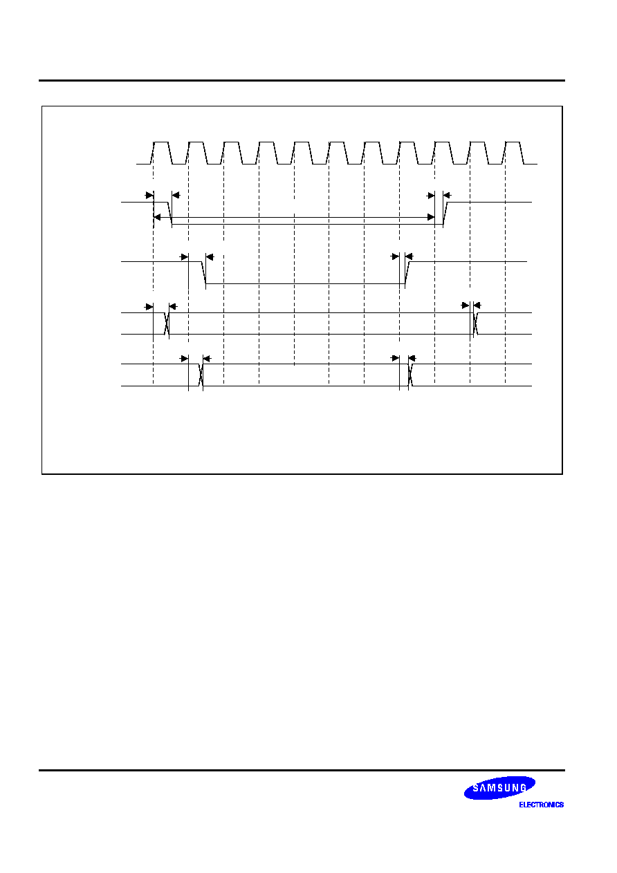
MEMORY CONTROLLER
S3C2501X
5-30
nRCS
nSDWE
ADDR
DATA
Addr
HCLKO
tACC
Data
TACC = 0x8 (8 cycles)
TCOS = 0x0 (0 cycle)
TCOH = 0x0 (0 cycle)
TACS = 0x0 (0 cycle)
tADDRd
tRCSh
tnSDWEh
tADDRh
tDATAh
tRCSd
tnSDWEd
tDATAd
Figure 5-15. Write Timing Diagram 1

S3C2501X
MEMORY CONTROLLER
5-31
nRCS
nOE
ADDR
DATA
Addr
HCLKO
Data Fetch
tACC
Data
tCOH
tACS
tCOS
TACC = 0x5 (5 cycles)
TCOS = 0x1 (1 cycle)
TCOH = 0x1 (1 cycle)
TACS = 0x1 (1 cycle)
tRCSd
tnOEd
tADDRd
tDATAd
tRCSh
tnOEh
tADDRh
tDATAh
Figure 5-16. Read Timing Diagram 2

MEMORY CONTROLLER
S3C2501X
5-32
nRCS
nSDWE
ADDR
DATA
HCLKO
tACC
Data
tCOH
tACS
tCOS
TACC = 0x5 (5 cycles)
TCOS = 0x1 (1 cycle)
TCOH = 0x1 (1 cycle)
TACS = 0x1 (1 cycle)
tADDRd
tRCSh
tnSDWEh
tADDRh
tDATAh
tRCSd
tnSDWEd
tDATAd
Addr
Figure 5-17. Write Timing Diagram 2

S3C2501X
MEMORY CONTROLLER
5-33
nRCS
nOE
ADDR
DATA
HCLKO
TACC = 5 (5 cycles)
TCOS = 1 (1 cycle)
TCOH = 2 (2 cycle)
TACS = 1 (1 cycle)
COHDIS = 1(Enable)
Addr1 at Bank n
tACC
Data 1
tCOH
tACS
tCOS
Addr2 at Bank n
tACC
Data 2
tACS
tCOS
nSDWE
tCOH
< 1st access cycle at Bank n >
< 2nd access cycle at Bank n >
~
~
~
~
~
~
~
~
~
~
~
~
~
~
~
~
Figure 5-18. Read after Write at the Same Bank (COHDIS = 1)

MEMORY CONTROLLER
S3C2501X
5-34
nRCS
nOE
ALE
DATA
HCLKO
Data Fetch
tACC
Data
tCOH
tMA
tCOS
TACC = 0x4 (4 cycles)
TCOS = 0x1 (1 cycle)
TCOH = 0x1 (1 cycle)
TMA = 0x2 (2 cycles)
MBE = 1 (Enable)
Addr
tDATAd
tRCSd
tRCSh
tnOEh
tnOEd
tDATAh
tADDRh
tALEh
tALEd
tADDRd
Figure 5-19. Read Timing Diagram (Muxed Bus)

S3C2501X
MEMORY CONTROLLER
5-35
nRCS
nSDWE
ALE
DATA
HCLKO
Data Fetch
tACC
Data
tCOH
tMA
tCOS
TACC = 0x4 (4 cycles)
TCOS = 0x1 (1 cycle)
TCOH = 0x1 (1 cycle)
TMA = 0x2 (2 cycles)
MBE = 1 (Enable)
Addr
tDATAd
tGCSd
tGCSh
tnSDWEh
tnSDWEd
tDATAh
tADDRh
tALEh
tALEd
tADDRd
Figure 5-20. Write Timing Diagram (Muxed Bus)

MEMORY CONTROLLER
S3C2501X
5-36
nRCS
nSDWE
ADDR
DATA
Addr
HCLKO
tACC
tACS
tCOS
TACC = 0x5 (5 cycles)
TCOS = 0x1 (1 cycle)
TCOH = 0x0 (0 cycle)
TACS = 0x1 (1 cycle)
EWAITEN = 1 (Enable)
nEWAIT
/nReady
tnOEd
tADDRd
tADDRh
tnOEh
tDATAh
tRCSh
tRCSd
tDATAd
Data
tnWAITd
tnWAITh
Figure 5-21. Write Timing Diagram (nEWAIT)

S3C2501X
MEMORY CONTROLLER
5-37
nRCS
nSDWE
ADDR
DATA
HCLKO
tACC
tACS
tCOS
TACC = 0x5 (5 cycles)
TCOS = 0x1 (1 cycle)
TCOH = 0x0 (0 cycle)
TACS = 0x1 (1 cycle)
EWAITEN = 1 (Enable)
NREADY = 1 (nReady)
nEWAIT
/nReady
tDATAd
tRCSd
tnSDWEd
tADDRd
tDATAh
tADDRh
tnSDWEh
tRCSh
Data
tnWAITd
tnWAITh
Addr
Figure 5-22. Write Timing Diagram (nREADY)

MEMORY CONTROLLER
S3C2501X
5-38
5.7 SDRAM CONTROLLER
5.7.1 FEATURES
The SDRAM controller provides the following features:
∑
Provides merging write buffer to improve system performance.
∑
Supports for 16M-bit, 64M-bit, 128M-bit and 256M-bit SDRAM devices with two or four leaves.
∑
Allows a direct interface to up to two banks of SDRAM.
∑
Each bank supports 16 or 32 bits wide and up to 128M-byte in size.
∑
Support byte, half-word and word transaction.
∑
CAS latency can be 1, 2 or 3
∑
Provides auto refresh and self refresh mode to sustain the contents of SDRAM memory.

S3C2501X
MEMORY CONTROLLER
5-39
5.7.2 SDRAM SIZE AND CONFIGURATION
The SDRAM controller supports a SDRAM memory ranging from 2 to 256M-byte. Table 5-19. Illustrates the
supported SDRAM configurations when external bus width is 32 bits. Table 5-20. Illustrates the supported
SDRAM configurations when external bus width is 16 bits.
If 16M-bit device, which has two leaves, is used, only ADDR[13] is used to select a leaf.
If SDRAM device, which has four leaves, is used, both ADDR[14] and ADDR[13] are used to select a leaf.
Only the chip select signals (nSDCS[1:0]) are to select a bank. The other SDRAM control signals are common to
both banks.

MEMORY CONTROLLER
S3C2501X
5-40
Table 5-19. Supported SDRAM Configuration of 32-bit External Bus
SDRAM
Technology
SDRAM
Arrangement
# Banks
Address Size
Leaf Select
Total
Memory Size
Row
Col
ADDR[14]
ADDR[13]
(Byte)
16M-bit
2M x 8
1
11
9
≠
HADDR[21]
8 M
2
16 M
1M x16
1
11
8
≠
HADDR[21]
4 M
2
8 M
64M-bit
8M x 8
1
12
9
HADDR[22]
HADDR[21]
32 M
2
64 M
4M x 16
1
12
8
HADDR[22]
HADDR[21]
16 M
2
32 M
2M x 32
1
11
8
HADDR[22]
HADDR[21]
8 M
2
16 M
128M-bit
16M x 8
1
12
10
HADDR[22]
HADDR[21]
64 M
2
128 M
8M x 16
1
12
9
HADDR[22]
HADDR[21]
32 M
2
64 M
4M x 32
1
12
8
HADDR[22]
HADDR[21]
16 M
2
32 M
256M-bit
32M x 8
1
13
10
HADDR[22]
HADDR[21]
128 M
2
256 M
16M x 16
1
13
9
HADDR[22]
HADDR[21]
64 M
2
128 M
8M x 32
1
13
8
HADDR[22]
HADDR[21]
32 M
2
64 M
NOTE: Banks: Number of external SDRAM memory bank used.
The controller supports up to two banks.
Leaf:
Internal bank of SDRAM devices.

S3C2501X
MEMORY CONTROLLER
5-41
Table 5-20. Supported SDRAM Configuration of 16-bit External Bus
SDRAM
Technology
SDRAM
Arrangement
# Banks
Address Size
Leaf Select
Total
Memory Size
Row
Col
ADDR[14]
ADDR[13]
(Byte)
16M-bit
2M x 8
1
11
9
≠
HADDR[20]
4 M
2
8 M
1M x16
1
11
8
≠
HADDR[20]
2 M
2
4 M
64M-bit
8M x 8
1
12
9
HADDR[21]
HADDR[20]
16 M
2
32 M
4M x 16
1
12
8
HADDR[21]
HADDR[20]
8 M
2
16 M
128M-bit
16M x 8
1
12
10
HADDR[21]
HADDR[20]
32 M
2
64 M
8M x 16
1
12
9
HADDR[21]
HADDR[20]
16 M
2
32 M
256M-bit
32M x 8
1
13
10
HADDR[21]
HADDR[20]
64M
2
128M
16M x 16
1
13
9
HADDR[21]
HADDR[20]
32 M
2
64 M
NOTE: Banks: Number of external SDRAM memory bank used.
The controller supports up to two banks
Leaf :
Internal bank of SDRAM devices.

MEMORY CONTROLLER
S3C2501X
5-42
5.7.3 ADDRESS MAPPING
Table 5-21. Illustrates the AHB address bus to the SDRAM address ADDR[14:0] mapping for various memory
devices when external bus width is 32 bits. Table 5-22. Illustrates the AHB address bus to the SDRAM address
ADDR[14:0] mapping for various memory devices when external bus width is 16 bits.
Table 5-21. SDRAM Address Mapping of 32-bit External Bus
SDRAM
Column Address (AddrOut[14:0])
Technology
14
13
12
11
10
9
8
7
6
5
4
3
2
1
0
16M-bit
2Mx8
*
21
*
*
AP
*
22
9
8
7
6
5
4
3
2
1Mx16
*
21
*
*
*
*
9
8
7
6
5
4
3
2
64M-bit
8Mx8
22
21
*
*
*
24
9
8
7
6
5
4
3
2
4Mx16
22
21
*
*
*
*
9
8
7
6
5
4
3
2
2Mx32
22
21
*
*
*
*
9
8
7
6
5
4
3
2
128M-bit
16Mx8
22
21
*
*
25
24
9
8
7
6
5
4
3
2
8Mx16
22
21
*
*
*
24
9
8
7
6
5
4
3
2
4Mx32
22
21
*
*
*
*
9
8
7
6
5
4
3
2
256M-bit
32Mx8
22
21
*
*
26
25
9
8
7
6
5
4
3
2
16Mx16
22
21
*
*
*
25
9
8
7
6
5
4
3
2
8Mx32
22
21
*
*
*
*
9
8
7
6
5
4
3
2
SDRAM
Row Address (AddrOut[14:0])
Technology
14
13
12
11
10
9
8
7
6
5
4
3
2
1
0
16M-bit
2Mx8
*
21
*
*
20
19
18
17
16
15
14
13
12
11
10
1Mx16
*
21
*
*
20
19
18
17
16
15
14
13
12
11
10
64M-bit
8Mx8
22
21
*
23
20
19
18
17
16
15
14
13
12
11
10
4Mx16
22
21
*
23
20
19
18
17
16
15
14
13
12
11
10
2Mx32
22
21
*
*
20
19
18
17
16
15
14
13
12
11
10
128M-bit
16Mx8
22
21
*
23
20
19
18
17
16
15
14
13
12
11
10
8Mx16
22
21
*
23
20
19
18
17
16
15
14
13
12
11
10
4Mx32
22
21
*
23
20
19
18
17
16
15
14
13
12
11
10
256M-bit
32Mx8
22
21
24
23
20
19
18
17
16
15
14
13
12
11
10
16Mx16
22
21
24
23
20
19
18
17
16
15
14
13
12
11
10
8Mx32
22
21
24
23
20
19
18
17
16
15
14
13
12
11
10

S3C2501X
MEMORY CONTROLLER
5-43
Table 5-22. SDRAM address mapping of 16-bit external bus
SDRAM
Column Address (AddrOut[14:0])
Technology
14
13
12
11
10
9
8
7
6
5
4
3
2
1
0
16M-bit
2Mx8
*
20
*
*
AP
*
21
8
7
6
5
4
3
2
1
1Mx16
*
20
*
*
*
*
8
7
6
5
4
3
2
1
64M-bit
8Mx8
21
20
*
*
*
23
8
7
6
5
4
3
2
1
4Mx16
21
20
*
*
*
*
8
7
6
5
4
3
2
1
128M-bit
16Mx8
21
20
*
*
24
23
8
7
6
5
4
3
2
1
8Mx16
21
20
*
*
*
23
8
7
6
5
4
3
2
1
256M-bit
32Mx8
21
20
*
*
25
24
8
7
6
5
4
3
2
1
16Mx16
21
20
*
*
*
24
8
7
6
5
4
3
2
1
SDRAM
Row Address (AddrOut[14:0])
Technology
14
13
12
11
10
9
8
7
6
5
4
3
2
1
0
16M-bit
2Mx8
*
20
*
*
19
18
17
16
15
14
13
12
11
10
9
1Mx16
*
20
*
*
19
18
17
16
15
14
13
12
11
10
9
64M-bit
8Mx8
21
20
*
22
19
18
17
16
15
14
13
12
11
10
9
4Mx16
21
20
*
22
19
18
17
16
15
14
13
12
11
10
9
128M-bit
16Mx8
21
20
*
22
19
18
17
16
15
14
13
12
11
10
9
8Mx16
21
20
*
22
19
18
17
16
15
14
13
12
11
10
9
256M-bit
32Mx8
21
20
23
22
19
18
17
16
15
14
13
12
11
10
9
16Mx16
21
20
23
22
19
18
17
16
15
14
13
12
11
10
9
NOTE: AP: Auto precharge (enable and disable auto precharge function are controlled by this bit).
At precharge command this bit controls the all bank or specified bank to be precharged.
Shaded numbers: leaf selection bits.
*: unused bits

MEMORY CONTROLLER
S3C2501X
5-44
5.7.4 SDRAM COMMANDS
The SDRAM controller issues specific commands to the SDRAM devices by encoding the nSDCS, nSDRAS,
nSDCAS and nSDWE outputs. Table 5-23. Lists all of the SDRAM commands understood by SDRAM devices.
The controller supports a subset of these commands.
Table 5-23. SDRAM commands
Command
CKE
nSDCS
nSDRAS nSDCAS
nSDWE
BA
A10/AP Mnemonic
Mode Register Set (MRS)
H
L
L
L
L
OP code
MRS
Refresh
Auto refresh
H
L
L
L
H
X
REF
Self refresh
L
L
L
L
H
SREF
Row activate
H
L
L
H
H
V
X
ACT
Read
with auto
precharge
H
L
H
L
H
V
H
RDA
without auto
precharge
L
RD
Write
with auto
precharge
H
L
H
L
L
V
H
WRA
without auto
precharge
L
WR
Burst stop
H
L
H
H
L
X
BST
Precharge
Bank selection
H
L
L
H
L
V
L
PRE
All banks
X
H
PALL
Active power down
L
H
X
X
X
X
APWDN
Precharge power down
L
H
X
X
X
PPWDN
No operation
H
H
H
H
H
NOP
NOTE: Shaded boxes indicate commands not supported by SDRAM controller. They are included for completeness.
X = Don't care
V = Valid value (H or L)
A10/AP = ADDR[10] /Auto Pre-charge

S3C2501X
MEMORY CONTROLLER
5-45
5.7.5 EXTERNAL DATA BUS WIDTH
The SDRAM controller supports not only 32 bit data bus, but also 16 bit data bus. External data bus width can be
selected by the XW field of CFGREG.
5.7.6 MERGING WRITE BUFFER
A merging write buffer compacts the writes of all widths into quad-word, which can be efficiently transferred to
the SDRAM. The merging write buffer improves the data bandwidth of write operation. The merging write buffer
is comprised of write buffer 0 and write buffer 1. Each write buffer holds a quad word, which is the size of the
default SDRAM data burst length. Two write buffer configuration allows a new quad word to be buffered while the
contents of the other quad-word buffer are transferred to memory. These write buffers can also merge non-
contiguous writes to the same quad word address.
The conditions of the write buffer flush are as follows:
∑
Write miss: there is a write to a SDRAM address outside the current merging quad word address
∑
Read hit: there is a read from the same address as the merging quad word.
∑
Write buffer time out: the write buffer timer reaches zero.
∑
The write buffer is disabled.
When a read hit, the write-back operation is completed before the requested data is read from memory to
maintain data consistency between the write buffer and SDRAM memory.
5.7.7 SELF REFRESH
The SDRAM controller provides the auto refresh (REF) and self refresh (SREF) command to sustain the contents
of the SDRAM. The auto refresh is issued to SDRAM periodically when refresh timer is expired. The self refresh
is entered and exited by request of on-chip power manager. The self refresh is the preferred refresh mode for
data retention and low power operation of SDRAM. In self refresh mode the SDRAM ignores all the input signals
except CKE. The refresh addressing and timing are internally generated to reduced power consumption.
Before disabling clock of the SDRAM controller the SDRAM must be in self refresh mode to sustain the SDRAM
memory data. Self refresh mode might be entered or exited by asserting or deasserting the self refresh request
bit (SRreg) of the peripheral clock disable register (PLCKDIS).
It is possible to know if the SDRAM is in self refresh mode or not by reading out the SRreg bit SRack bit of the
PCLKDIS register.
If the self refresh mode change is on processing, the SRack bit of the PCLKDIS is deasserted, and if the self
refresh mode, change is completed, the SRack bit is asserted.
To recover from the self refresh mode to normal operation mode, the SRack bit shoul be checked asserted
before access the SDRAM.

MEMORY CONTROLLER
S3C2501X
5-46
5.7.8 BASIC OPERATION
SDRAM initialization sequence
On power-on reset, software must initialize the SDRAM controller and each of the SDRAM connected to the
controller. Refer to the SDRAM data sheet for more detailed information on the start up procedure for the
SDRAM used. Typical example sequence is given below :
1.
Wait 200us to allow SDRAM power and clocks to stabilize.
2.
Program the INIT[1:0] of the CFGREG to 01. This automatically issues a PALL command to the SDRAM.
3.
Write 0xF into the refresh timer register. This provides a refresh cycle every 15 clock cycles.
4.
Wait for a time period equivalent to 120 clock cycles (8 refresh cycles).
5.
Program the normal operational value into the refresh timer.
6. Program the CFGREG to their normal operation values.
7. Program the INIT[1:0] to 10. This automatically issues a MRS command to the SDRAM.
8.
Program the INIT[1:0] to 00. The controller enters the normal mode.
9.
Program the CMDREG and WBTOREG to their normal operation values.
10. The SDRAM is now ready for normal operation.

S3C2501X
MEMORY CONTROLLER
5-47
5.7.9 SDRAM SPECIAL REGISTERS
The address and reset value of the special regsiters in the SDRAM controller summarized in Table 5-24.
Table 5-24. SDRAM Special Registers
Name
Address
Description
Reset value
CFGREG
0xF0020000
Configuration register
0x00099F0C
CMDREG
0xF0020004
Command register
0x00000000
REFREG
0xF0020008
Refresh timer register
0x00000020
WBTOREG
0xF002000C
Write buffer time-out register
0x00000000
5.3.9.1 Configuration Register
The configuration register is 32-bit read/write (some bits are read only) register. This register contains SDRAM
control parameters such as external bus width, memory type, and various timing parameters.
Table 5-25. SDRAM Configuration Register
Registers
Address
R/W
Description
Reset value
CFGREG
0xF0020000
R/W
SDRAM Configuration register
0x00099F0C

MEMORY CONTROLLER
S3C2501X
5-48
Table 5-25 SDRAM Configuration Register (Continue)
Reg0
Bit
Description
R/W
Default
value
XW
[0]
External data bus Width
0 = external bus width is 32 bit.
1 = external bus width is 16 bit.
R/W
0
AP
[1]
Auto Pre-charge control for SDRAM accesses
0 = Auto pre-charge
1 = No auto pre-charge
R/W
0
CL
[3:2]
CAS Latency
00 = Reserved 01 = CL: 1 cycle
10 = CL: 2 cycles 11 = CL: 3 cycles
R/W
11
D1[1:0]
[5:4]
SDRAM device Density of bank 1
00 = 16M-bit SDRAM memory devices.
01 = 64M-bit SDRAM memory devices.
10 = 128M-bit SDRAM memory devices.
11 = 256M-bit SDRAM memory devices.
R/W
00
D0[1:0]
[7:6]
SDRAM device Density of bank 0
00 = 16M-bit SDRAM memory devices.
01 = 64M-bit SDRAM memory devices.
10 = 128M-bit SDRAM memory devices.
11 = 256M-bit SDRAM memory devices.
R/W
00
RP
[9:8]
Row Pre-charge time
00 = RP: 1 cycle 01 = RP: 2 cycles
10 = RP: 3 cycles 11 = RP: 4 cycles
R/W
11
RCD
[11:10]
RAS to CAS delay
00 = RCD: 1 cycle 01 = RCD: 2 cycles
10 = RCD: 3 cycles 11 = RCD: 4 cycles
R/W
11
RC
[15:12]
Row Cycle
0000 = RC: 1 cycles 0001 = RC: 2 cycles
...
1110 = RC: 15 cycles 1111 = RC: 16 cycles
R/W
1001
RAS
[19:16]
Row Active time
0000 = RAS: 1 cycles 0001 = RAS: 2 cycles
...
1110 = RAS: 15 cycles 1111 = RAS: 16 cycles
R/W
1001
[31:20]
Reserved
≠
NOTES:
1.
Software should not write to configuration register when the SDRAM engine is busy. The SDRAM engine status bit,
BUSY in command register, can be used to check if the control engine is idle.
2.
We recommend that the auto pre-charge should be disable by asserting "1" on the AP of Reg0 when the page hit ratio is
more than 50%.

S3C2501X
MEMORY CONTROLLER
5-49
[0] eXternal data bus Width : XW
0 = external bus width is 32 bit ,1 = external bus width is 16 bit
[1] Auto Pre-charge control for SDRAM accesses: AP
0 = Auto pre-charge ,
1 = No auto pre-charge
[3:2] CAS Latency: CL
00 = Reserved
01 = 1 cycles
10 = 2 cycles
11 = 3 cycles
[5:4] SDRAM device Density of bank 1: D1
00 = 16 Mbit SDRAM memory devices.
01 = 64 Mbit SDRAM memory devices.
10 = 128 Mbit SDRAM memory devices.
11 = 256 Mbit SDRAM memory devices.
[7:6] SDRAM device Density of bank 0: D0
00 = 16 Mbit SDRAM memory devices.
01 = 64 Mbit SDRAM memory devices.
10 = 128 Mbit SDRAM memory devices.
11 = 256 Mbit SDRAM memory devices.
[9:8] Row Pre-charge time: RP
00 = 1 cycle
01 = 2 cycles
10 = 3 cycles
11 = 4 cycles
[11:10] RAS to CAS delay: RCD
00 = 1 cycle
01 = 2 cycles
10 = 3 cycles
11 = 4 cycles
[15:12] Row Cycle: RC
0000 = 1 cycle
0001 = 2 cycles
0010 = 3 cycles
0011 = 4 cycles
0100 = 5 cycles
0101 = 6 cycles
0110 = 7 cycles
0111 = 8 cycles
1000 = 9 cycles
1001 = 10 cycles
1010 = 11 cycle
1011 = 12 cycles
1100 = 13cycles
1101 = 14 cycles
1110 = 15 cycles
1111 = 16 cycles
[19:16] Row Active time: RAS
0000 = 1 cycle
0001 = 2 cycles
0010 = 3 cycles
0011 = 4 cycles
0100 = 5 cycles
0101 = 6 cycles
0110 = 7 cycles
0111 = 8 cycles
1000 = 9 cycles
1001 = 10 cycles
1010 = 11 cycle
1011 = 12 cycles
1100 = 13cycles
1101 = 14 cycles
1110 = 15 cycles
1111 = 16 cycles
[31:20] Reserved
31
0
3
4
5
1
2
20 19
15
10 9
16
12 11
8 7
6
RESERVED
RC
D1
X
W
A
P
CL
D0
RP
RCD
RAS
Figure 5-23. SDRAM Configuration Register

MEMORY CONTROLLER
S3C2501X
5-50
5.7.9.2 Command Register
The configuration register 1 is 32-bit read/write (some bits are read only) register. The SDRAM initialization
command, write buffer operation can be controlled by this register.
Table 5-26. SDRAM Command Register
Registers
Address
R/W
Description
Reset value
CMDREG
0xF0020004
R/W
SDRAM command register
0x00000000
CMDREG
Bit
Description
R/W
Default value
INIT
[1:0]
Control bits for SDRAM device initialization
00 = Normal operation
01 = Automatically issue a PALL to the SDRAM
10 = Automatically issue a MRS to the SDRAM
11 = reserved
R/W
00
WBUF
[2]
Write buffer enable
0 = Disable merging write buffer
1 = Enable merging write buffer
NOTE: Disabling the write buffer will flush any stored
value(s) to the external SDRAM memory
R/W
0
BUSY
[3]
SDRAM controller status bit
0 = SDRAM controller is idle
1 = SDRAM controller is busy
R
0
[31:4]
Reserved
NOTE: WBUF field of configuration register is a read-only bit if write buffers are not included in an AHB interface sub-block

S3C2501X
MEMORY CONTROLLER
5-51
[1:0] Control bits for SDRAM device initialization :
00 = Normal operation
01 = Automatically issue a PALL to the SDRAM
10 = Automatically issue a MRS to the SDRAM
11 = reserved
[2] Write buffer enable:
0 = Disable merging write buffer
1 = Enable merging write buffer
[3] SDRAM controller status bit:
0 = SDRAM controller is idle
1 = SDRAM controller is busy
[31:4] Reserved
31
0
3
4
1
2
RESERVED
B
U
I
N
T
B
S
Y
Figure 5-24. SDRAM Command Register

MEMORY CONTROLLER
S3C2501X
5-52
5.7.9.3 Refresh Timer Register
The Refresh timer register is 32-bit read/write (some bits are read only) register. This register sets the SDRAM
refresh cycle. The refresh timer register is programmed with the number of system bus clock that should be
counted between SDRAM refresh cycles.
Table 5-27. SDRAM Refresh Timer Register
Registers
Address
R/W
Description
Reset value
REFREG
0xF0020008
R/W
Refresh timer register
0x00000020
REFREG
Bit
Description
R/W
Default value
REFCYC
[15:0]
SDRAM refresh cycle
R/W
0x00000020
[31:16]
Reserved
For example, for common refresh period of 15.6us, and a system bus clock frequency of 66MHz:
15.6 x 10
-6
x 66 x 10
6
= 1029
The refresh timer is set to 64 on reset. To ensure a refresh interval of less than 15.6us after reset, The minimum
frequency of system bus clock allowed is:
64 / (15.6 x 10
-6
)= 4.3 MHz
The refresh register should be written to as early as possible in the system start-up procedure, especially when
clock frequency is very low.
[15:0] SDRAM refresh cycle
[31:16] Reserved
0
15
RESERVED
REFCYC
Figure 5-25. SDRAM Refresh Timer Register

S3C2501X
MEMORY CONTROLLER
5-53
5.7.9.4 Write Buffer Time-out Register
The write buffer time-out register works with the merging write buffer (if write buffer is enabled). This 16-bit
read/write field of register sets the cycles for a forced flush of the write buffer.
Table 5-28. SDRAM Write Buffer Time-out Register
Registers
Address
R/W
Description
Reset value
WBTOREG
0xF002000C
R/W
Write buffer time-out register
0x00000000
WBTOREG
Bit
Description
R/W
Default value
WBTO
[15:0]
Write buffer time-out delay time
R/W
0x00000000
[31:16]
Reserved
≠
A write to a merging write buffer loads the value in the timeout register into the time-out down counter of the
buffer. When the time-out counter reaches 0 the merging write buffer contents is written(flushed) to the external
memory. The down counter is clocked by system bus clock. Storing a value of 0 in the timeout register disables
the write buffer timeout function.
[15:0] Write buffer time-out delay time:
[31:16] Reserved
31
0
15
16
RESERVED
WBTO
Figure 5-26. SDRAM Write Buffer Time-out Register

MEMORY CONTROLLER
S3C2501X
5-54
5.7.10 SDRAM CONTROLLER TIMING
Read
ADDR
DATA
HCLKO
nSDCAS
nSDWE
CKE
nSDRAS
nSDCS
DQM/
nWBE
Row Active
Row Addr.
tCC
tCL
tCH
tCSd
tCSh
tRASd
tRASh
tADDRd
tCASd
tCASh
tADDRh
tRDd
tRDh
tDQMd
tDQMh
tRCD
Col. Addr.
Data
DQM
Latency
CAS
Latency
Figure 5-27. Single Read Operation (CAS Latency=2)

S3C2501X
MEMORY CONTROLLER
5-55
Read
ADDR
DATA
HCLKO
nSDCAS
nSDWE
CKE
nSDRAS
nSDCS
DQM/
nWBE
Row Active
Row Addr.
tCC
tCL
tCH
tCSd
tCSh
tRASd
tRASh
tADDRd
tCASd
tCASh
tADDRh
tRDd
tRDh
tDQMd
tDQMh
tRCD
Col. Addr.
Data
DQM
Latency
CAS Latency
Figure 5-28. Single Read Operation (CAS Latency=3)

MEMORY CONTROLLER
S3C2501X
5-56
Write
ADDR
DATA
HCLKO
nSDCAS
nSDWE
nSDRAS
nSDCS
Data
Row Active
Row Addr.
tCC
tCL
tCSd
tCSh
tRASd
tRASh
tADDRd
tCASd
tCASh
tADDRh
tWDd
tWDh
tDQMd
tDQMh
tRCD
tWEd
tWEh
DQM /
nWBE
Col. Addr.
CKE
tCH
Figure 5-29. Single Write Operation

S3C2501X
MEMORY CONTROLLER
5-57
Col. Addr.
Data
Data
Data
Data
Write
ADDR
DATA
HCLKO
nSDCAS
nSDWE
CKE
nSDRAS
nSDCS
Row Active
Row Addr.
tRCD
tCC
tCL
tCH
tCSd
tCSh
tRASd
tRASh
tADDRd
tCASd
tCASh
tADDRh
tRDh
tDQMd
tDQMh
CAS Latency
DQM Latency
tRDd
DQM/
nWBE
Figure 5-30. Burst Read Operation (CAS Latency = 2)

MEMORY CONTROLLER
S3C2501X
5-58
Read
ADDR
DATA
Col. Addr.
HCLKO
nSDCAS
nSDWE
CKE
nSDRAS
nSDCS
Row Active
Row Addr.
tCC
tCL
tCH
tCSd
tCSh
tRASd
tRASh
tADDRd
tCASd
tCASh
tADDRh
tRDd
tRDh
tDQMd
tDQMh
tRCD
Data
Data
Data
Data
DQM /
nWBE
CAS Latency
DQM Latency
Figure 5-31. Burst Read Operation (CAS Latency = 3)

S3C2501X
MEMORY CONTROLLER
5-59
Col. Addr.
Data
Data
Write
ADDR
DATA
HCLKO
nSDCAS
nSDWE
CKE
nSDRAS
nSDCS
DQM/
nWBE
Row Active
Row Addr.
tRCD
tCC
tCL
tCH
tCSd
tCSh
tRASd
tRASh
tADDRd
tCASd
tCASh
tADDRh
tWDh
tDQMd
tDQMh
tWDd
Data
Data
tWEd
tWEh
Figure 5-32. Burst Write Operation

MEMORY CONTROLLER
S3C2501X
5-60
NOTES

S3C2501X
I
2
C CONTROLLER
6-1
6
I
2
C CONTROLLER
6.1 OVERVIEW
The S3C2501X has internal I
2
C (or IIC) controller. It requires only two bus lines, a serial data line (SDA) and a
serial clock lines (SCL). When the I
2
C is free, both lines are high level. It is connected to the same I
2
C. And the
number of IC is limited only by the maximum bus capacitance of 400 pF.
6.2 FEATURES
∑
Supports only single master mode.
∑
Supports 8-bit, bi-directional, serial data transfers.
∑
Supports 7-bit addressing.
Figure 6-1 shows a block diagram of the S3C2501X I
2
C controller
Data
Control
Serial Clock
Line Control
Serial
Clock
Prescaler
Control status register (IICCON)
RESET
BUSY
COND1 COND0
ACK
LRB
IEN
Prescaler register (IICPS)
System clock (f
SYSCLK
)
16
SCL
SDA
BF
Shift buffer register (IICBUF)
Figure 6-1. I
2
C Block Diagram

I
2
C CONTROLLER
S3C2501X
6-2
6.3 FUNCTIONAL DESCRIPTION
The S3C2501X I
2
C controller is the master of the serial I
2
C. Using a prescaler register, the user can program the
serial clock frequency that is supplied to the I
2
C controller. The serial clock frequency is calculated as follows:
Serial clock frequency = f
SYSCLK
/ (16
◊
(prescaler register value + 1) + 3)
, where f
SYSCLK
is the system clock frequency.
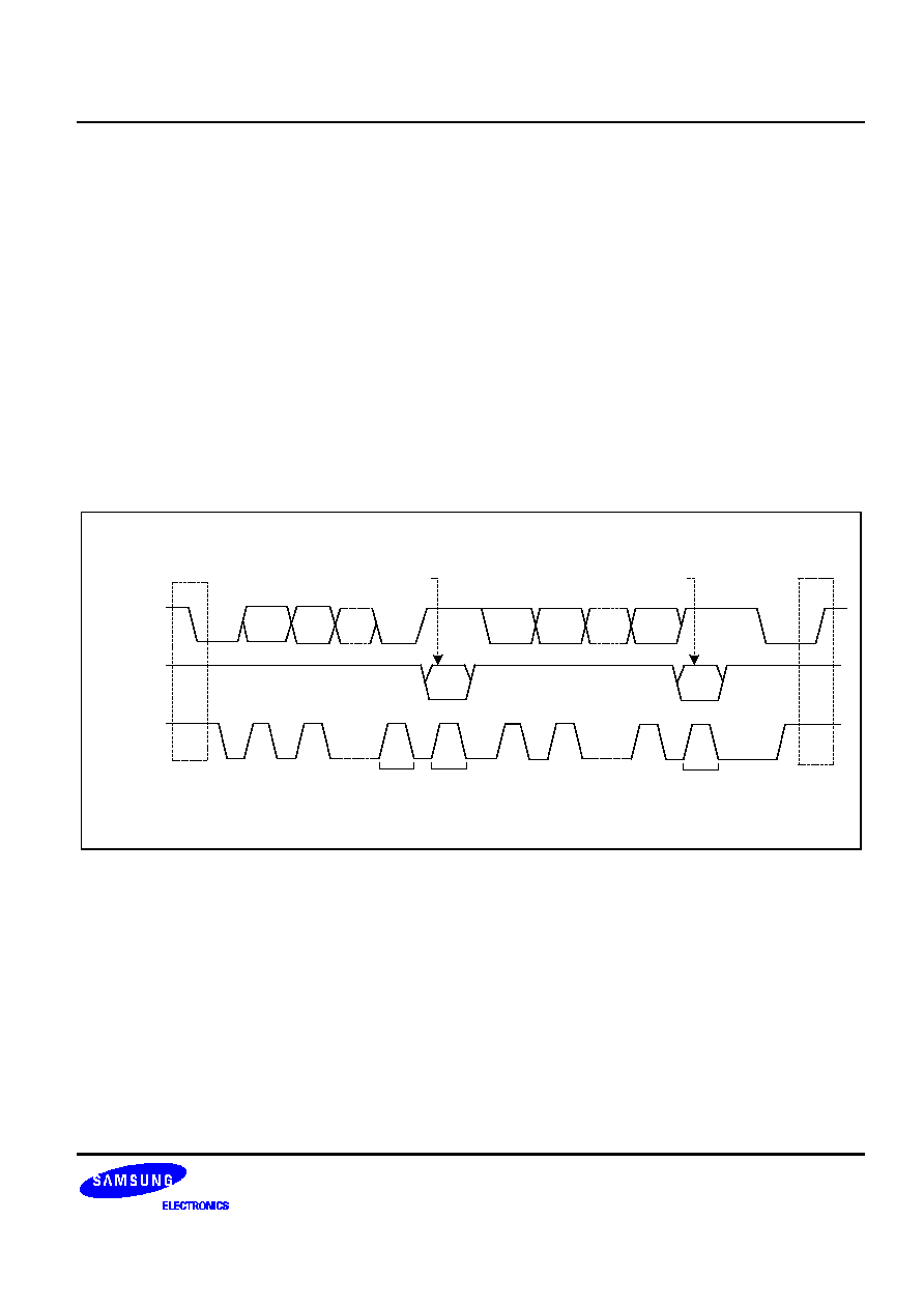
S3C2501X
I
2
C CONTROLLER
6-3
6.4 I
2
C CONCEPTS
6.4.1 BASIC OPERATION
The I
2
C has two wires, a serial data line (SDL) and a serial clock line (SCL), to carry information between the IC's
connected to the bus. Each IC is recognized by a unique address and can operate as either a transmitter or
receiver, depending on the function of the specific IC's.
The I
2
C is a multi-master bus. This means that more than ICs which are capable of controlling the bus can be
connected to it. Data transfers proceed as follows:
Case 1: A master IC wants to send data to another IC (slave):
1.
Master addresses slave
2.
Master sends data to the slave (master is transmitter, slave is receiver)
3.
Master terminates the data transfer
Start
Condition
Address
P
9
Stop
Condition
SDA by
Receiver
SCL from
Master
8
9
8
R/W
ACK
ACK
S
SDA by
Transmitter
MSB
Acknowledge
from receiver
Acknowledge
from receiver
2
1
MSB
Data
2
1
Figure 6-2. Master Transmitter and Slave Receiver
Case 2: A master IC wants to receive information from another IC (slave):
1.
Master addresses slave
2.
Master receives data from the slave (master is receiver, slave is transmitter)
3.
Master terminates the data transfer

I
2
C CONTROLLER
S3C2501X
6-4
Start
Condition
Address
P
9
Stop
Condition
SDA by
Receiver
SCL from
Master
8
9
8
R/W
ACK
ACK
S
SDA by
Transmitter
MSB
Acknowledge
from receiver
Acknowledge from
transmitter
2
1
MSB
Data
2
1
Figure 6-3. Master Receiver and Slave Transmitter
Even in this case, the master IC generates the timing and terminates the transfer.
The master IC is always responsible for generating the clock signals on the I
2
C. Bus clock signals from a master
can only be altered by 1) a slow slave IC which "stretches" the signal by temporarily holding the clock line Low, or
2) by another master IC during arbitration.
6.4.2 GENERAL CHARACTERISTICS
Both SDA and SCL are bi-directional lines which are connected to a positive supply voltage through a pull-up
resistor.
When the I
2
C is free, the SDA and SCL lines are both high level. The output stages of I
2
C interfaces connected
to the bus have an open-drain or open-collector to perform the wired-AND function. Data on the I
2
C can be
transferred at a rate up to 100 Kbits/s. The number of interfaces that can be connected to the bus is solely
dependent on the limiting bus capacitance of 400 pF.
6.4.3 BIT TRANSFERS
Due to the variety of different IC's (CMOS, NMOS, and I2L, for example) which can be connected to the I
2
C, the
levels of logic zero (low) and logic one (high) are not fixed and depend on the associated level of V
DD
. One clock
pulse is generated for each data bit that is transferred.

S3C2501X
I
2
C CONTROLLER
6-5
6.4.4 DATA VALIDITY
The data on the SDA line must be stable during the high period of the clock. The high or low state of the data line
can only change when clock signal on the SCL line is low.
6.4.5 START AND STOP CONDITIONS
Start and stop conditions are always generated by the master. The bus is considered to be busy after the start
condition is generated. The bus is considered to be free again when a brief time interval has elapsed following
the stop condition.
-- Start condition: a High-to-Low transition of the SDA line while SCL is high.
-- Stop condition: a Low-to-High transition of the SDA line while SCL is high.
Start
Condition
Address
P
9
Stop
Condition
SDA
SCL
1-7
8
9
1-7
8
9
1-7
8
R/W
ACK
DATA
ACK
DATA
ACK
S
Figure 6-4. Start and Stop Conditions

I
2
C CONTROLLER
S3C2501X
6-6
6.4.6 DATA TRANSFER OPERATIONS
6.4.6.1 Data Byte Format
Every data byte that is put on the SDA line must be 8 bits long. The number of bytes that can be transmitted per
transfer is unlimited. Each byte must be followed by an acknowledge bit. Data is transferred MSB-first.
If the receiver cannot receive another complete byte of data until it has performed some other functions (such as
servicing an internal interrupt), it can hold the clock line SCL low to force the transmitter into a wait state. The
data transfer then continues when the receiver is ready for another byte of data and releases the SCL line.
6.4.6.2 Acknowledge Procedure
Data transfer with acknowledge is obligatory. The acknowledge-related clock pulses must be generated by the
bus master. The transmitter releases the SDA line (High) during the acknowledge clock pulse.
The receiver must pull down the SDA line during the acknowledge pulse so that it remains stable low during the
high period of this clock pulse.
Usually, a receiver which has been addressed is obliged to generate an acknowledge after each byte is received.
When a slave receiver does not acknowledge from the slave address, the slave must leave the data line high.
The master can then generate a stop condition to abort the transfer.
If a slave receiver acknowledges the slave address, but later in the transfer cannot receive any more data bytes,
the master must again abort the transfer. This is indicated by the slave not generating the acknowledge on the
first byte to follow. The slave leaves the data line high and the master generates the stop condition.
If a master receiver is involved in a transfer, it must signal the end of data to the slave transmitter by not
generating an acknowledge on the last byte that was clocked out of the slave. The slave transmitter must then
release the data line to let the master generate the stop condition.

S3C2501X
I
2
C CONTROLLER
6-7
6.4.6.3 Data Transfer Format
Data transfers uses the format shown in Figure 6-5. After the start condition has been generated, a 7-bit slave
address is sent. The eighth bit is a data direction bit (R/W). A "0" direction bit indicates a transmission (Write)
and a "1" indicates a request for data (Read).
A data transfer is always terminated by a stop condition which is generated by the master. However, if a master
still wishes to communicate on the bus, it can generate another start condition and address another slaves
without first generating a stop condition. This feature supports the use of various combinations of read/write
formats for data transfers.
S
Slave address
A
Data 1 (8 bits)
A
Data 2
Data M
A
N
A
K
P
S
Slave address
A
Data 1 (8 bits)
A
Data 2
Data M
A
A P
Multiple byte master receiver format:
Multiple byte master transmitter format:
W
R
NOTE:
(Start)
(Write; bit value is 0)
(Read; bit value is 1)
(Stop),
(Acknowledge; The ACK is first sent from the slave. Afterwards, the direction
depends on the data transfer direction. In other words, if the mater reads the
data, it sends the ACK.)
(Not Acknowledge)
S
W
R
P
A
NAK
Figure 6-5. Data Transfer Format
6.4.6.4 I
2
C Addressing
The addressing procedure for the I
2
C is such that the first byte after the start condition determines which slave
the master will select. Usually, this first byte immediately follows the start procedure.
An exception is the "general call" address which can address all ICs simultaneously. When this address is used,
all ICs should, in theory, respond with an acknowledge. However, ICs can also be made to ignore this address.
The second byte of the general call address then defines the action to be taken.
6.4.6.5 Definition of Bits in the First Data Byte
The first seven bits of the first data byte make up the slave address. The eighth bit is the LSB, or direction bit,
which determines the direction (R/W) of the message.
When an address is sent, each IC on the bus compares the first 7 bits received following start condition with its
own address. If the addresses match, the IC considers itself addressed by the master as a slave receiver or a
slave transmitter.

I
2
C CONTROLLER
S3C2501X
6-8
6.5 I
2
C SPECIAL REGISTERS
The I
2
C controller has three special registers: a control status register (IICCON), a prescaler register (IICPS), and
a shift buffer register (IICBUF).
6.5.1 CONTROL STATUS REGISTER (IICCON)
The control status register for the I
2
C, IICCON, is described in Table 6-2.
Table 6-1. Control Status Register (IICCON)
Register
Address
R/W
Description
Rest Value
IICCON
0xF00F0000
R/W
Control status register
0x00000000
Table 6-2. IICCON Register Description
Bit Number
Bit Name
Description
[0]
Buffer flag (BF)
The BF bit is set when the buffer is empty in transmit mode or
when the buffer is full in receive mode. To clear the buffer, you
write a "0" to this bit. The BF bit is cleared automatically
whenever the IICBUF register is written or read.
[1]
Interrupt enable (IEN)
Setting the interrupt enable bit to "1" enables the I
2
C interrupt.
An interrupt is generated if BF bit set to 1.
[2]
Last received bit (LRB)
The LRB bit is read only. It holds the value of the last received bit
over the I
2
C. Normally, this bit will be the value of the slave
acknowledgement. To check for slave acknowledgement, you
test the LRB.
[3]
Acknowledge enable (ACK)
The ACK bit is normally set to "1". This causes the I
2
C controller
to send an acknowledge automatically after each byte. This bit
must be "0" when the I
2
C controller is operating in receiver mode
and requires no further data to be received from the slave
transmitter. This causes a negative acknowledge on the I
2
C,
which halts further reception from the slave device.
[5:4]
COND1, COND0
These bits control the generation of the start, stop, and repeat
start conditions: "00" = no effect, "01" = start, "10" = stop, and
"11" = repeat start. When start condition, BF bit should be set
simultaneously. When repeated start condition, ACK bit should
be set simultaneously
[6]
Bus busy (BUSY)
This bit is a read-only flag that indicates when the I
2
C is in use. A
"1" indicates that the bus is busy. This bit is set or cleared by a
start or stop condition, respectively.
[7]
Reset
If "1" is written to the reset bit, the I
2
C controller is reset to its
initial state.
[31:8]
Reserved
Not applicable.

S3C2501X
I
2
C CONTROLLER
6-9
[0] Buffer Flag (BF)
0 = Automatically cleared when the IICBUF register is written or read. To manually
clear the BF, write 0.
1 = Automatically set when the buffer is empty in transmit mode or when the buffer
is full in receive mode.
[1] Interrupt enable (IEN)
0 = Disable
1 = Enable; an interrupt is generated if the BF bit is 1.
[2] Last received bit (LRB)
Use this read-only status bit to check for ACK signals from the receiver (slave), or
to monitor SDA operation of SDA when writing 11 to IICCON [5:4] for repeated
starts.
0 = The most recent SDA is low. (ACK is received)
1 = The most recent SDA is high. (ACK not received)
[3] Acknow enable (ACK)
Controls generation of an ACK signal in receive mode.
0 = Do not generate an ACK at 9th SCL (No more received data is required from
the slave)
1 = Generate an ACK signal at 9th SCL.
[5:4] COND 1 and COND 0
Generate a control such as start or stop.
00 = No effect.
01 = Generate start condition. (BF bit should be set simultaneously)
10 = Generate stop condition.
11 = SCL will be released to high level to generate repeated start condition.
(ACK bit should be set simultaneously)
[6] Bus busy (BUSY)
Data transmission is in progress on the IIC-bus.
0 = Bus is currently not in use. (not busy)
1 = Bus is in use. (busy)
[7] Reset
0 = Normal
1 = Reset the IIC controller.
[31:8] Reserved
I
E
N
L
R
B
A
C
K
C
O
N
D
0
C
O
N
D
1
B
U
S
Y
R
E
S
E
T
Reserved
31
8
7
0
6
5
4
3
2
1
B
F
Figure 6-6. I
2
C Control Status Register

I
2
C CONTROLLER
S3C2501X
6-10
6.5.2 SHIFT BUFFER REGISTER (IICBUF)
Table 6-3. IICBUF Register
Register
Address
R/W
Description
Rest Value
IICBUF
0xF00F0004
R/W
Shift buffer register
Undefined
Bit Number
Bit Name
Description
[7:0]
Data
This data field acts as serial shift register and read buffer for interfacing to
the I
2
C. All read and write operations to/from the I
2
C are done via this
register. The IICBUF register is a combination of a shift register and a data
buffer. 8-bit parallel data is always written to the shift register, and read form
the data buffer. I
2
C data is always shifted in or out of the shift register.
[31:8]
Reserved
Not applicable.
6.5.3 PRESCALER REGISTER (IICPS)
Table 6-4. IICPS Register
Register
Address
R/W
Description
Rest Value
IICPS
0xF00F0008
R/W
Prescaler register
0x00000000
Bit Number
Bit Name
Description
[15:0]
Prescaler value
This prescaler value is used to generate the serial I
2
C clock. The system
clock is divided by (16 x (prescaler value + 1) + 3) to make the serial I
2
C
clock. If the prescaler value is zero, the system clock is when divided by 19
to make the serial I
2
C clock. Therefore, when I
2
C is used to 100kbit/s in the
standard mode, the prescaler value must be changed.
[31:16]
Reserved
Not applicable.

S3C2501X
I
2
C CONTROLLER
6-11
6.5.4 PRESCALER COUNTER REGISTER (IICCNT)
Table 6-5. IICCNT Register
Register
Address
R/W
Description
Rest Value
IICCNT
0xF00F000C
R/W
Prescaler counter register
0x00000000
Bit Number
Bit Name
Description
[15:0]
Counter value
This 16-bit value is the value of the prescaler counter. It is read (in test
mode only) to check the counter's current value.
[31:16]
Reserved
Not applicable.
6.5.5 INTERRUPT PENDING REGISTER (IICPND)
Table 6-6. IICPND Register
Register
Address
R/W
Description
Rest Value
IICPND
0xF00F0010
R/W
Interrupt pending register
0x00000000
Bit Number
Bit Name
Description
[0]
Interrupt pending
value
This bit is set when the interrupt is generated and cleared when the same
value of interrupt pending bit is rewritten.
[31:1]
Reserved
Not applicable.

I
2
C CONTROLLER
S3C2501X
6-12
IIC Setup
(Reset, IICPS Setup)
IICCON = Start | BF
IICBUF = IIC Slave Address | 0x0
IICBUF = IIC Upper Address
IICBUF = IIC Lower Address
IICBUF = One Byte Data
ALL Data Sent?
IICCON = Stop
Yes
No
Figure 6-7. Write Operation Flow Chart
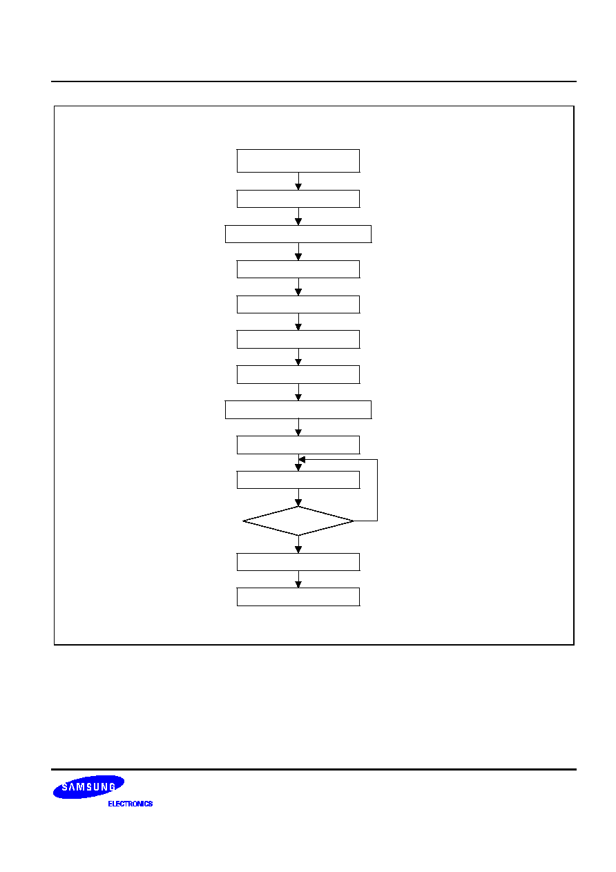
S3C2501X
I
2
C CONTROLLER
6-13
IIC Setup
(Reset, IICPS Setup)
IICCON = Start | BF
IICBUF = IIC Slave Address | 0x0
IICBUF = IIC Upper Address
IICBUF = IIC Lower Address
IICBUF = One Byte Data
ALL Data Receive?
Send No ACK
Yes
No
IICCON = Repeat Start | ACK
IICCON = Start | ACK
IICBUF = IIC Slave Address | 0x1
Empty the BF Bit
IICCON = Stop
Figure 6-8. Read Operation Flow Chart

I
2
C CONTROLLER
S3C2501X
6-14
NOTES

S3C2501X
ETHERNET CONTROLLER
7-1
7
ETHERNET CONTROLLER
7.1 OVERVIEW
The S3C2501X has two Ethernet controllers that operate at either 100M-bit or 10M-bit per second in half-duplex
or full-duplex mode. In half-duplex mode, the IEEE 802.3 carrier sense multiple access with collision detection
(CSMA/CD) protocol is supported. In full-duplex mode, the IEEE 802.3 MAC control layer is also supported,
including the pause operation for flow control.
The two Ethernet controllers support both the media independent interface (MII) and the buffered DMA interface
(BDI). The MAC layer consists of a receiver and a transmitter blocks, a flow control block, a content addressable
memory(CAM) for storing network addresses, a number of commands, status, and error counter registers.
The MII supplies the transmission and reception clocks of 25MHz for 100M-bps operation, 2.5 MHz for the 10M-
bps speed or 1MHz for (the 1M-bps for) Home PNA. The MII conforms to the ISO/IEC 802-3 standards.
B
D
I
M
I
I
/
10
M
b
p
s
7
-
W
i
r
e
MAC
TxFIFO
(80x9)
MAC
Preamble/
SFD/CRC/
PAD/JAM
Generator
MAC
RxFIFO
(16x10)
CAM
Checker
(32x32)
CRC
Checker
MAC Control and
Status
Station
Manager
M
D
I
BDMA
PHYSICAL
LAYER
Preamble/
SFD
Detector
Backoff
and
Intergap
timer
Flow Control
BDMA Tx
Buffer
Controller
BDMA Tx
Buffer
(64 words)
Bus Arbiter/
Controller
BDMA Rx
Buffer
(64 words)
BDMA Rx
Buffer
Controller
CAM
Contents
Memory
(32-words)
BDMA
Control
and Satus
register
32
32
32
32
32
32
S
Y
S
T
E
M
B
U
S
Figure 7-1. Ethernet Diagram

ETHERNET CONTROLLER
S3C2501X
7-2
7.2 FEATURES
The most important features and benefits of each Ethernet controller are as follows:
∑
Cost-effective connection to an external NIC/Ethernet backbone
∑
Buffered DMA (BDMA) engine with burst mode
∑
BDMA Tx/Rx Buffers (BTxBUFF and BRxBUFF: 256 bytes/256 bytes)
∑
MAC Tx/Rx FIFOs(MTxFIFO and MRxFIFO: 80 bytes/16 bytes) to support re-transmission after collision
without DMA request and DMA latency
∑
Data alignment logic
∑
Old and new physical media support (compatible with existing 10M-bps networks)
∑
100M-bps or 10M-bps operation to allow price/performance options and to support phased conversions
∑
Full IEEE 802.3 compatibility for existing applications
∑
Media Independent interface (MII) or 7-wire interface
∑
Station management (STA) signaling for external physical layer configuration and link negotiation
∑
On-chip CAM (21 MAC addresses)
∑
Full-duplex mode for doubled bandwidth
∑
Hardware support of pause operation for full-duplex flow control
∑
Long frame mode for specialized environment
∑
Short frame mode for fast testing
∑
PAD generation for easy processing and reduced processing time

S3C2501X
ETHERNET CONTROLLER
7-3
7.3 MAC FUNCTION BLOCKS
The major function blocks of each Ethernet of MAC layer are described in Table 7-1 and Figure 7-1.
Table 7-1. MAC Function Block Descriptions
Function Block
Description
Media Independent
Interface (MII)
The interface between the physical layer and the transmit/receiver blocks.
Transmitter block
Moves the outgoing data from the transmit buffer to the MII. This includes circuits
for generating the CRC, checking parity, and generating preamble or jam.
Also has timers for back-off after collision and the inter-frame gap follows a
transmission.
Receiver block
Accepts incoming data from the MII and stores it in the MRxFIFO. The receiver
block has logic for computing and checking the CRC value, generating parity for
data from the MII, and checking minimum and maximum frame lengths.
Also has a CAM that provides for address lookup, and for acceptance or rejection
for frame based on their destination address.
Flow control block
Recognizes MAC-control frame and supports the pause operation for full-duplex
links. The flow control block also supports generation of pause frame, and
provides timers and counters for pause control.
MAC control (command)
and status registers
Controls programmable options, including the enabling or disabling of signals that
notify the system when conditions occur. The status registers hold information for
error handling software, and the error counters accumulate statistical information
for network management software.
Loop-back circuit
Provides for MAC-layer testing in isolation from the MII and physical layer.
7.3.1 MEDIA INDEPENDENT INTERFACE (MII)
Both transmitter and receiver blocks operate using the MII, which was developed by the IEEE802.3 task force on
100-Mbps Ethernet. This interface has the following characteristics:
∑
Media independence
∑
Multi-vendor points of interoperability
∑
Supports connection of MAC layer and physical layer entity (PHY) devices
∑
Capable of supporting both 100M-bps and 10M-bps and 1M-bps data rates
∑
Data and delimiters are synchronous to clock references
∑
Provides independent 4-bit wide transmit and receive data paths
∑
Uses TTL signal levels that are compatible with common digital CMOS ASIC processes
∑
Supports connection of PHY layer and station management (STA) devices
∑
∑
Provides a simple management interface
∑
∑
Capable of driving a limited length of shielded cable

ETHERNET CONTROLLER
S3C2501X
7-4
7.3.2 PHYSICAL LAYER ENTITY (PHY)
The physical layer entity, or PHY, performs all of the decoding/encoding on incoming and outgoing data. The
manner of decoding and encoding (Manchester for 10BASE-T, 4B/5B for 100BASE-X, or 8B/6T for 100BASE-T4)
does not affect the MII. The MII provides the raw data it receives, starting with the preamble and ending with the
CRC. The MII expects raw data for transmission, also starting with the preamble and ending with the CRC. The
MAC layer also generates jam data and transmits it to the PHY.
7.3.3 BUFFERED DMA INTERFACE (BDI)
The buffered DMA interface (BDI) supports read and write operations across the system bus. Two eight-bit buses
transfer data with optional parity checking. The system interface initiates data transfers. The MAC-layer controller
responds with a ready signal to accept data for transmission, or to deliver data which has been received. An end-
of-frame signal indicates the boundary between packets.
7.3.4 THE MAC TRANSMITTER BLOCK
The MAC transmitter block is responsible for transmitting data. It complies with the IEEE802.3 standard for the
carrier sense multiple access with collision detection (CSMA/CD) protocol.
7.3.4.1 MAC TxFIFO(MTxFIFO)
The MTxFIFO has an 80-byte depth. An extra bit is associated with each data byte for parity checking. This
80-byte by 9-bit size allows the first 64 bytes of a data frame to be stored and retransmitted, without further
system involvement, in case of a collision. If no collision occurs and transmission is underway, the additional 16
bytes handle system latency and avoid FIFO under-run.
When the system interface has set the MACTXCON.0 bit, the transmission state machine requests data from the
BDI. The system controller then fetches data from the system memory.
The data is stored in the MTxFIFO until the threshold for transmit data is satisfied. When the MTxFIFO is not full,
a request is issued to the BDI for more data. It then appends the calculated CRC to the end of the data (unless
the CRC truncate bit in the transmit control register is set).
7.3.4.2 Preamble and Jam Generator
As soon as the MACTXCON.0 bit is set and there are eight bytes of data in the MTxFIFO, the transmission state
machine starts the transmission by asserting the TX_EN signal and transmitting the preamble and the start frame
delimiter (SFD). In case there is a collision, it transmits a 32-bit string of `1's after the preamble as a jam pattern.
7.3.4.3 PAD Generator
If a short data frame is transmitted, the MAC will normally generate pad bytes to extend the frame to a minimum
of 64 bytes. The pad bytes consist entirely of `0' bits. A control bit is also used to suppress the generation of pad
bytes.
7.3.4.4 Parallel CRC Generator
The CRC generation of the outgoing data starts from the destination address and continues through the data
field. You can suppress CRC generation by setting the appropriate bit in the transmit control register. This is
useful in testing, for example, to force the transmission of a bad CRC in order to test error detection in the
receiver. It can also be useful in certain bridge or switch applications, where end-to-end CRC checking is desired.

S3C2501X
ETHERNET CONTROLLER
7-5
7.3.4.5 Threshold Logic and Counters
The transmission state machine uses a counter and logic to control the threshold of when the transmission can
begin. Before transmitting the MAC waits until eight bytes or a complete frame has been placed in the
MTxFIFO. This gives the DMA engine some latency without causing an underflow during transmission.
7.3.4.6 Back-Off and Retransmit Timers
When a collision is detected on the network, the transmitter block stops the transmission and starts a jamming
pattern to ensure that all the nodes detect the collision. After this, the transmitter waits for a minimum of 96 bit
times and then retransmits the data. After 16 attempts, the transmission state machine sets an error bit and
generates an interrupt, if enabled, to signify the failure to transmit a frame due to excessive collisions. It flushes
the MTxFIFO, and the MAC is ready for the next frame.
7.3.4.7 Transmit Data Parity Checker
Data in the FIFO is even-parity. When data is read for transmission, the transmission state machine checks the
parity. If a parity error is detected, the transmit data parity checker does the following:
∑
It stops transmission.
∑
∑
It sets the parity error bit in the transmit status register.
∑
It generates an interrupt, if enabled.
7.3.4.8 Transmission State Machine
The transmission state machine is the central control logic for the transmitter block. It controls the passing of
signals, the timers, and the posting of errors in the status registers.

ETHERNET CONTROLLER
S3C2501X
7-6
7.3.5 THE MAC RECEIVER BLOCK
It complies with the IEEE802.3 standard for carrier sense multiple access with collision detection (CSMA/CD)
protocol.
After it receives a frame, the receiver block checks for a number of error conditions: CRC errors, alignment
errors, and length errors. By setting bits in appropriate control registers some error condition is disabled.
Depending on the CAM status, the destination address and the receiver block may reject an otherwise
acceptable frame.
7.3.5.1 MAC RxFIFO (MRxFIFO)
The MRxFIFO accepts data one byte at a time. The parity starts with the destination address. The receiver
updates the counter with the number of bytes received. As the FIFO stores the data, the CAM block checks the
destination address against its stored address. If the CAM recognizes the address, the MRxFIFO continues
receiving the frame. If the CAM block does not recognize the address and rejects the frame, the receiver block
discards the frame and flushes the MRxFIFO.
7.3.5.2 CAM and Address Recognition
The CAM compares the destination address of the received frame to stored addresses. If it finds a match, the
receive state machine continues to receive the frame. The CAM is organized to hold six-byte address entries.
The CAM can store 21 address entries.
The CAM address entries 0, 1, and 18 are used to send the pause control frame. To send a pause control frame,
you must write the destination address to CAM0, the source address to CAM1, and length/type, op-code, and
operand to the CAM18 entry. You must write the MAC transmit control register to set the send pause control bit.
In addition, CAM19 and CAM20 can be used to construct a user-define control frame.
7.3.5.3 Parallel CRC Checker
The receiver block computes a CRC across the data and the transmitted CRC, and then checks that the resulting
syndrome is valid. A parallel CRC checking scheme handles data arriving in 4-bit nibbles at 100M-bps. To
support full-duplex operation, the receiver and transmitter blocks have independent CRC circuits.
7.3.5.4 Receive State Machine
In MII mode, the receiver block receives data from the MII on the RXD[3:0] lines. This data is synchronized to
RX_CLK at 25 MHz or 2.5MHz. In 7-wire mode, and at 10MHz, data is received on the RXD_10M line only.
After it detects the preamble and SFD, the receive state machine arranges data in byte configurations, generates
parity, and stores the result in the MRxFIFO one byte at a time. If the CAM block accepts the destination
address, the MRxFIFO stores the rest of the frame. Any error in reception will reset the MRxFIFO and the state
machine will wait for the end of the current frame. It will then be idle while it is waiting for the next preamble and
SFD.
7.3.5.5 BDMA Interface Receive State Machine
The BDMA I/F receive state machine issues the Rx_rdy signal whenever data is present in the receive FIFO. The
last byte of the packet is signaled by asserting the Rx_EOF.
In case there are any errors during the reception, or if there is a CRC error at the end, the BDMA I/F receive
state machine asserts the Rx_toss signal to indicate that the received packet should be discarded.

S3C2501X
ETHERNET CONTROLLER
7-7
7.3.6 FLOW CONTROL BLOCK
Flow control is done using the MAC control frame. The receiver sends control frames to the transmitter and the
transmitter pauses its operation during the time interval specified in the control frames. The flow control block
provides the following functions:
∑
Recognition of MAC control frames received by the receiver block
∑
Transmission of MAC control frames, even if transmitter is paused
∑
Timers and counters for pause operation
∑
∑
Command and status register (CSR) interface
∑
∑
Options for passing MAC control frames through to software drivers
For details, refer to the full-duplex pause operation section in this chapter.
7.3.7 BUFFERED DMA (BDMA) OVERVIEW
The BDMA engine controls the data feeding and reception between the MAC and the system bus (AMBA) using
two buffers, BDMA TxBUFF (BTxBUFF) and BDMA RxBUFF (BRxBUFF). The BTxBUFF and BRxBUFF hold
data and status information for frames being transmitted and received, respectively. Each buffer is controlled by
the block, which consists of a bus arbiter, a control and status block, buffer descriptors.
7.3.7.1 Bus Arbiter
The bus arbiter decides which of the BDMA buffer controllers, transmit (Tx) or receive (Rx), has the highest
priority for accessing the system bus. The prioritization is dynamic. The BDMA arbiter outputs a bus request
signal (nREQ) to the AMBA when Rx Buffer (BRxBUFF) contains 4-words data, or EOF (End of Frame) was
saved to the buffer, or Tx Buffer (BTxBUFF) contains 4-word free space.
After it receives a bus acknowledgement signal (nACK) from the AMBA, the BDMA bus arbiter determines the
correct bus access priority.

ETHERNET CONTROLLER
S3C2501X
7-8
7.3.7.2 Control and Status
This block controls the read/write operations of the bus master across the AMBA. The control logic supports the
following operations:
-- Fixed 4-word burst size control between Tx and Rx.
-- Transmit threshold control (based on 1/8 of transmit buffer size) to match transmission latency to system bus
latency.
-- Little-Endian byte swapping, to support the data transfer of Little-Endian memory usage for frame data.
-- A transmit/receive alignment widget to circumvent word alignment restrictions.
The beginning of a frame should be placed on word boundary. Misalignment of the BDMA transfer would
complicate the design of the DMA and degrade the performance. To avoid this, you can use an alignment widget
between the BDMA Buffer (word) and the MAC FIFO (byte) by controlling the widget field in Tx buffer descriptor.
The widget discards the first 'n' bytes (up to three), where 'n' is the value read from the Tx buffer descriptor that
configures the alignment widget.
In the receiver, the BDMA bus arbiter inserts a programmable number of bytes (up to three) into the received
data stream while the preamble is being received. This adds some padding to the beginning of the frame. This
padding can then be used to solve the alignment problem without having to use a copy of the buffer. Because
the data is inserted prior to the concatenation of bytes into words, it does not misalign the subsequent DMA
transfer. The number of the alignment bytes is read from the BDMARXCON.5-4 (BRxWA).

S3C2501X
ETHERNET CONTROLLER
7-9
7.3.7.3 Buffer Descriptor
The ownership bit in the buffer descriptor controls the owner of the descriptor. When the ownership bit is '1', the
BDMA controller owns the descriptor. When the bit is '0', the CPU owns the descriptor. The owner of the
descriptor always owns the associated data frame. (The descriptor's frame start address field always points to
this frame.)
Software sets the BDMARXLEN register to the length, and also sets the BDMARXDPTR register to point to a
chain of buffer descriptors, all of which have their ownership bits set.
The BDMA engine can then be started to set the BDMARXCON.10 (BRxEn). When a frame is received, it is
copied into the external memory at the address specified by the BDMARXDPTR register. Please note that no
configurable offset or page boundary calculation is required. The received frame is written into the buffer in the
external memory until the end of frame is reached, or until the length exceeds the configured maximum frame
size. If the entire frame is received successfully, the status bits in the buffer descriptor are set to indicate this.
Otherwise, the status bits are set to indicate that an error occurred. The ownership bit in the status and length
field is cleared and an interrupt may now be generated. The length field in the Rx buffer descriptor is updated in
summation with previous length filed of Rx buffer descriptor. The BDMA points the next buffer descriptor
automatically, but BDMATXDPTR and BDMARXDPTR is not updated to the next pointer. It always has the first
buffer descriptor address. Because BDMA pointers are fixed as initial addresses, BDMA count register values
indicate the number of frames to be handled by BDMA.
In addition, users can determine how many buffer descriptors to use by controlling the BDMATXCON.3~0
(BTxNBD) and BDMARXCON.3-0 (BRxNBD). If the last buffer descriptor was used by the BDMA, the next buffer
is the first buffer and BDMA count register value goes to zero. Finally, the status and length fields in the first and
the last Rx buffer descriptors are updated. The length field value is same in the first and last Rx buffer descriptor.
The status field of the middle Rx buffer descriptors does not have any mean.
When the received frame size exceeds the maximum frame size (BRxMFS bits of BDMARXLEN), the data
frame will be overwritten by the last word of maximum frame. If overflow occurred, this status is written to status
field bit.20 in the Rx buffer descriptor. When the BDMA reads a descriptor, if the ownership bit is not set, it has
two options:
-- Skip to the next buffer descriptor, or
-- Generate an interrupt and halt the BDMA operation. If CPU set to skip bit in Rx buffer descriptor's status
field, BDMA goes next buffer without interrupt or BDMA stop.
During transmission, the two-byte frame length at the Tx buffer descriptor is moved into the BDMA internal Tx
counter. After transmission, Tx status is saved in the Tx buffer descriptor. The BDMA points to the next buffer
descriptor address register for the linked list structure. However, BDMATXDPTR register cannot be updated.
You should check BTXBDCNT register to detect how many frames were handled.

ETHERNET CONTROLLER
S3C2501X
7-10
[31:0]
Buffer pointer
Address of the data be transmitted.
[31]
Ownership bit (O)
0 = CPU
1 = BDMA
[30:18]
TxStatus
Writing in this field don't have any mean.
[30] Reserved
[29] Paused
Transmission of frame was paused due to the reception of a Pause control frame.
[28] Halted
The transmission of the next frame is halted when MACCON.1 (MHaltImm) is set,
or when MACTXCON.0 (MTxEn) is clear.
[27] SQEErr
Signal Quality Error
[26] Defer
The transmission of frame was deferred.
[25] Coll
The collision is occured in half-duplex. The current frame is retried to send.
[24] Comp
The transmition is finished.
[23] ParErr
MTxFIFO Parity Error
[22] LateColl
The Collision occured after 64 byte times.
[21] NoCarr
No Carrier sense is detected when MAC Tx transmits a frame.
[20] DeferErr
MAC doesn't run the transmission process until 6071-nibble or 24284-bit times.
The current frame is aborted.
[19] Underflow
MTxFIFO underflow
[18] ExColl
The excessive collision is occured 16 times consecutively.
The current frame is aborted.
[17:16]
TxWidget
The transmission widget alignment of the current frame.
[15:0]
TxLength
The size of the transmission data by using the BDMA.
The Unit of the length field is the byte and the hexdecimal number.
31
15
0
Buffer Pointer
16
30
O
TxStatus
18 17
TxWidget
TxLength
Figure 7-2. Data Structure of Tx Buffer Descriptor

S3C2501X
ETHERNET CONTROLLER
7-11
[31:0]
Buffer pointer
Address of the frame data be saved.
[31]
Ownership bit (O)
0 = CPU
1 = BDMA
[30]
Skip BD (B)
Set this bit to skip the current buffer descriptor when the ownership bit is cleared.
[29]
SOF (S)
Set by the BDMA to indicate the first BD for a frame.
[28]
EOF (E)
Set by the BDMA to indicate the last BD for a frame.
[27]
Done (D)
Set by the BDMA on the first BD when the reception of a frame finished
and it used multiple BD's.
[26:16]
Rx status
The Rx status field of the received frame.
[26] MSO
Rx frame size is larger than the Maximum Rx Frame Size(BRxMFS).
[25] Halted
The reception of next frame is halted when MACCON.1 (MHaltImm) is set,
or when MACRXCON.0 (MRxEn) is clear.
[24] MRx10Stat
The frame was received over 10Mbps(wire-7) interface.
[23] BRxDone
The reception process by the BDMA is done without error.
[22] RxParErr
MRxFIFO Parity Error
[21] MUFS
Set when the size of the Rx frame is larger than the Maximum Untagged Frame
Size(1518bytes) if the long packet is not enabled in the MAC Rx control register.
[20] Overflow
MRxFIFO Overflow
[19] CRCErr
CRC at the end of a frame did not match the computed CRC32, or else that
PHY asserted RX_ER during the frame reception.
[18] AlignErr
Set if the frame length in bit is not the multiple of eight and the CRC is invalid.
[17] Reserved
[16] Reserved
[15:0]
RxLength
The byte count of the received data is written in hexa-decimal by the BDMA.
31
15
0
Buffer Pointer
16
30
O
Status
RxLength
B S E D
29 28 27 26
Figure 7-3. Data Structure of Rx Buffer Descriptor

ETHERNET CONTROLLER
S3C2501X
7-12
Buffer
Descriptor
Start Address
Register
buffer #1
buffer #2
buffer #N
Memory for frame
BRXBDCNT+0
+
NOTE:
The BRxBS and BRxMFS of the BDMARXLEN register have to keep multiples of 16 in byte unit.
For long packet reception larger than 1518-byte, the BRxBS should be at least 4 bytes larger
than the BRxMFS or less than 1518-byte for the reception with a single or multiple buffer
descriptors, respectively.
BRxBS of
BDMARXLEN
not used
BRxBS of
BDMARXLEN
BRxBS of
BDMARXLEN
Memory for Rx bufer descriptor
not used
not used
BRXBDCNT+(N-1)
BRXBDCNT+1
buffer pointer #1
status
length
buffer pointer #2
status
length
buffer pointer #N
status
length
.
.
.
.
.
.
.
.
.
.
.
.
.
.
.
.
.
.
Figure 7-4. Data Structure of the Receive Frame

S3C2501X
ETHERNET CONTROLLER
7-13
7.4 ETHERNET CONTROLLER SPECIAL REGISTERS
There are two Ethernet controllers in S3C2501X. They are same each other except the base addresses for
internal registers.
Table 7-2. ETHERNET 0 Special Registers
Registers
Address
R/W
Description
Reset Value
BDMATXCONA
0xF00A0000
R/W
Buffered DMA transmit control register
0x00000000
BDMARXCONA
0xF00A0004
R/W
Buffered DMA receive control register
0x00000000
BDMATXDPTRA
0xF00A0008
R/W
Transmit buffer descriptor start address
0x00000000
BDMARXDPTRA
0xF00A000C
R/W
Receive buffer descriptor start address
0x00000000
BTXBDCNTA
0xF00A0010
R/W
BDMA Tx buffer descriptor counter
0x00000000
BRXBDCNTA
0xF00A0014
R/W
BDMA Rx buffer descriptor counter
0x00000000
BMTXINTENA
0xF00A0018
R/W
BDMA/MAC Tx Interrupt enable register
0x00000000
BMRXINTENA
0xF00A001C
R/W
BDMA/MAC Rx Interrupt enable register
0x00000000
BMTXSTATA
0xF00A0020
R/W
BDMA/MAC Tx Status register
0x00000000
BMRXSTATA
0xF00A0024
R/W
BDMA/MAC Rx Status register
0x00000000
BDMARXLENA
0xF00A0028
R/W
Receive Frame Size
0x00000000
CFTXSTATA
0xF00A0030
R
Transmit control frame status
0x00000000
MACCONA
0xF00B0000
R/W
MAC control
0x00000000
CAMCONA
0xF00B0004
R/W
CAM control
0x00000000
MACTXCONA
0xF00B0008
R/W
Transmit control
0x00000000
MACTXSTATA
0xF00B000C
R/W
Transmit status
0x00000000
MACRXCONA
0xF00B0010
R/W
Receive control
0x00000000
MACRXSTATA
0xF00B0014
R/W
Receive status
0x00000000
STADATAA
0xF00B0018
R/W
Station management data
0x00000000
STACONA
0xF00B001C
R/W
Station management control and address
0x00006000
CAMENA
0xF00B0028
R/W
CAM enable
0x00000000
MISSCNTA
0xF00B003C
R(Clr)/W Missed error count
0x00000000
PZCNTA
0xF00B0040
R
Pause count
0x00000000
RMPZCNTA
0xF00B0044
R
Remote pause count
0x00000000
CAMA
0xF00B0080-
0xF00B00FC
W
CAM content (32 words)
Undefined

ETHERNET CONTROLLER
S3C2501X
7-14
Table 7-3. ETHERNET 1 Special Registers
Registers
Address
R/W
Description
Reset Value
BDMATXCONB
0xF00C0000
R/W
Buffered DMA transmit control register
0x00000000
BDMARXCONB
0xF00C0004
R/W
Buffered DMA receive control register
0x00000000
BDMATXDPTRB
0xF00C0008
R/W
Transmit buffer descriptor start address
0x00000000
BDMARXDPTRB
0xF00C000C
R/W
Receive buffer descriptor start address
0x00000000
BTXBDCNTB
0xF00C0010
R/W
BDMA Tx buffer descriptor counter
0x00000000
BRXBDCNTB
0xF00C0014
R/W
BDMA Rx buffer descriptor counter
0x00000000
BMTXINTENB
0xF00C0018
R/W
BDMA/MAC Tx Interrupt enable register
0x00000000
BMRXINTENB
0xF00C001C
R/W
BDMA/MAC Rx Interrupt enable register
0x00000000
BMTXSTATB
0xF00C0020
R/W
BDMA/MAC Tx Status register
0x00000000
BMRXSTATB
0xF00C0024
R/W
BDMA/MAC Rx Status register
0x00000000
BDMARXLENB
0xF00C0028
R/W
Receive Frame Size
0x00000000
CFTXSTATB
0xF00C0030
R
Transmit control frame status
0x00000000
MACCONB
0xF00D0000
R/W
MAC control
0x00000000
CAMCONB
0xF00D0004
R/W
CAM control
0x00000000
MACTXCONB
0xF00D0008
R/W
Transmit control
0x00000000
MACTXSTATB
0xF00D000C
R/W
Transmit status
0x00000000
MACRXCONB
0xF00D0010
R/W
Receive control
0x00000000
MACRXSTATB
0xF00D0014
R/W
Receive status
0x00000000
STADATAB
0xF00D0018
R/W
Station management data
0x00000000
STACONB
0xF00D001C
R/W
Station management control and address
0x00006000
CAMENB
0xF00D0028
R/W
CAM enable
0x00000000
MISSCNTB
0xF00D003C
R(Clr)/W Missed error count
0x00000000
PZCNTB
0xF00D0040
R
Pause count
0x00000000
RMPZCNTB
0xF00D0044
R
Remote pause count
0x00000000
CAMB
0xF00D0080-
0xF00D00FC
W
CAM content (32 words)
Undefined

S3C2501X
ETHERNET CONTROLLER
7-15
7.4.1 BDMA RELATIVE SPECIAL REGISTER
7.4.1.1 Buffered DMA Transmit Control Register
Table 7-4. BDMATXCON Register
Registers
Address
R/W
Description
Reset Value
BDMATXCONA
0xF00A0000
R/W
Buffered DMA transmit control register
0x00000000
BDMATXCONB
0xF00C0000
R/W
Buffered DMA transmit control register
0x00000000
Bit Number
Bit Name
Description
[3:0]
BDMA Tx Number of Buffer
Descriptor (BTxNBD)
You can select number of buffer descriptor.
0000 = 2
0
, 0001 = 2
1
, 0010 = 2
2
,....., 11xx = 2
12
[6:4]
BDMA transmit to MAC Tx
start level (BTxMSL)
These bits determine when to move the data of the new frame in
the BDMA Tx Buffer (BTxBUFF) to the MAC TxFIFO (MTxFIFO)
at a new frame arrival.
000 means no wait, 001 means wait to fill 1/8 of the BDMA Tx
Buffer, 010 means wait to fill 2/8 of the buffer, and so on through
100, which means wait to fill 4/8 of the BDMA Tx Buffer.
NOTE: If the last data of the frame arrives in BDMA Tx Buffer,
the data transfer from the BDMA Tx Buffer to the MAC
TxFIFO starts immediately, regardless of the level of
these bits.
[8:7]
Reserved
Not applicable.
[9]
≠
Factorial test bit
[10]
BDMA Tx enable (BTxEn)
When the Tx enable bit is set to `1', the BDMA Tx block is
enabled. Even if this bit is disabled, buffer data will be moved to
the MAC TxFIFO until the BDMA TxBUFF underflows.
This bit is automatically cleared when the BDMA is not the owner.
NOTE: The BDMATXDPTR register must be assigned before this
bit is set.
[11]
BDMA Tx reset (BTxRS)
Set this bit to `1' to reset the BDMA Tx block.
[31:12]
Reserved

ETHERNET CONTROLLER
S3C2501X
7-16
7.4.1.2 Buffered DMA Receive Control Register
Table 7-5. BDMA RXCON Register
Register
Address
R/W
Description
Rest Value
BDMARXCONA
0xF00A0004
R/W
Buffered DMA receive control register
0x00000000
BDMARXCONB
0xF00C0004
R/W
Buffered DMA receive control register
0x00000000
Bit Number
Bit Name
Description
[3:0]
BDMA Rx Number of
Buffer
Descriptor (BRxNBD)
You can select number of buffer descriptor.
0000 = 2
0
, 0001 = 2
1
, 0010 = 2
2
,....., 11xx = 2
12
[5:4]
BDMA Rx word alignment
(BRxWA)
The Rx word alignment bits determine how many bytes are
invalid in the first word of each data frame. These invalid bytes
are inserted when the word is assembled by the BDMA.
`00' = No invalid bytes, `01' = 1 invalid byte,
`10' = 2 invalid bytes, and `11' = 3 invalid bytes.
[8:6]
Reserved
Not applicable.
[9]
≠
Factorial test bits
[10]
BDMA Rx enable (BRxEn)
When the Rx enable bit is set to `1', the BDMA Rx block is
enabled. Even if this bit is disabled, buffer data will be moved to
the BDMA RxBUFF until the MAC RxFIFO underflows.
This bit is automatically disabled when the BDMA is not the
owner.
NOTE: The buffer descriptor start address pointer must be
assigned before this bit is set.
[11]
BDMA Rx reset (BRxRS)
Set this bit to `1' to reset the BDMA Rx block.
[31:12]
Reserved

S3C2501X
ETHERNET CONTROLLER
7-17
7.4.1.3 BDMA Transmit Buffer Descriptor Start Address Register
Table 7-6. BDMATXDPTR Register
Registers
Address
R/W
Description
Reset Value
BDMATXDPTRA
0xF00A0008
R/W
BDMA Tx buffer descriptor base register
0x00000000
BDMATXDPTRB
0xF00C0008
R/W
BDMA Tx buffer descriptor base register
0x00000000
Bit Number
Bit Name
Description
[31:0]
BDMA transmit buffer
descriptor start address
The BDMA transmit buffer descriptor start address register
contains the address of the first buffer descriptor on the frame to
be sent.
7.4.1.4 BDMA Receive Buffer Descriptor Start Address Register
Table 7-7. BDMARXDPTR Register
Registers
Address
R/W
Description
Reset Value
BDMARXDPTRA
0xF00A000C
R/W
BDMA Rx buffer descriptor base register
0x00000000
BDMARXDPTRB
0xF00C000C
R/W
BDMA Rx buffer descriptor base register
0x00000000
Bit Number
Bit Name
Description
[31:0]
BDMA receive buffer
descriptor start address
The BDMA receive buffer descriptor start address register
contains the address of the first buffer descriptor on the frame to
be saved.

ETHERNET CONTROLLER
S3C2501X
7-18
7.4.1.5 BDMA Transmit Buffer Descriptor Counter
Table 7-8. BTXBDCNT Register
Registers
Address
R/W
Description
Reset Value
BTXBDCNTA
0xF00A0010
R/W
BDMA Tx buffer descriptor counter of Current
Pointer
0x00000000
BTXBDCNTB
0xF00C0010
R/W
BDMA Tx buffer descriptor counter of Current
Pointer
0x00000000
Bit Number
Bit Name
Description
[11:0]
BDMA Tx buffer descriptor
Counter
The maximum counter value is dependent on the BTxNBD of the
BDMATXCON register.
Buffer descriptor current address =
BDMATXDPTR + (BTXBDCNT<<3)
7.4.1.6 BDMA Receive Buffer Descriptor Counter
Table 7-9. BRXBDCNT Register
Registers
Address
R/W
Description
Reset Value
BRXBDCNTA
0xF00A0014
R/W
BDMA Rx buffer descriptor counter
of current pointer
0x00000000
BRXBDCNTB
0xF00C0014
R/W
BDMA Rx buffer descriptor counter
of current pointer
0x00000000
Bit Number
Bit Name
Description
[11:0]
BDMA Rx buffer descriptor
Counter
The maximum counter value is dependent on the BTxNBD of
the BDMATXCON register.
Buffer descriptor current address =
BDMARXDPTR + (BRXBDCNT<<3)

S3C2501X
ETHERNET CONTROLLER
7-19
7.4.1.7 BDMA/MAC Transmit Interrupt Enable Register
Table 7-10. BMTXINTEN Register
Registers
Address
R/W
Description
Reset Value
BMTXINTENA
0xF00A0018
R/W
BDMA/MAC Tx Interrupt Enable
0x00000000
BMTXINTENB
0xF00C0018
R/W
BDMA/MAC Tx Interrupt Enable
0x00000000
Bit Number
Bit Name
Description
[0]
Enable MAC Tx excessive
collision (ExCollIE)
This bit enables ExColl Interrupt.
[1]
Enable MAC Tx underflow
(UnderflowIE)
This bit enables Underflow interrupt.
[2]
Enable MAC Tx deferral
(DeferErrIE)
This bit enables DeferErr interrupt.
[3]
Enable MAC Tx no carrier
(NoCarrIE)
This bit enables NoCarr interrupt.
[4]
Enable MAC Tx late
collision (LateCollIE)
This bit enables LateColl interrupt.
[5]
Enable MAC Tx transmit
parity (TxParErrIE)
This bit enables TxParErr interrupt.
[6]
Enable MAC Tx completion
(TxCompIE)
This bit enables TxComp interrupt.
[15:7]
Reserved
Not applicable.
[16]
Tx complete to send control
frame interrupt enable
(TxCFcompIE)
This bit enable TxCFcomp interrupt.
[17]
BDMA Tx not owner
interrupt enable (BTxNOIE)
This bit enables BTxNO interrupt.
[18]
BDMA Tx Buffer empty
interrupt enable
(BTxEmptyIE)
This bit enables BTxEmpty interrupt
[31:19]
Reserved
Not applicable.

ETHERNET CONTROLLER
S3C2501X
7-20
7.4.1.8 BDMA/MAC Transmit Interrupt Status Register
Table 7-11. BMTXSTAT Register
Registers
Address
R/W
Description
Reset Value
BMTXSTATA
0xF00A0020
R/W
BDMA/MAC Tx Interrupt Status Register
0x00000000
BMTXSTATB
0xF00C0020
R/W
BDMA/MAC Tx Interrupt Status Register
0x00000000
Bit Number
Bit Name
Description
[0]
Excessive collision (ExColl) This bit is set when collision occurred 16 times consecutively. In
this case, the frame transmission is aborted. If this bit is the
cause of the interrupt, MTxEn/BTxEn/MReset bit should be
cleared for the re-transmission of the current frame.
[1]
Underflow
This bit is set if the MAC TxFIFO becomes empty during the
frame transmission.
[2]
Deferral Error (DeferErr)
This bit is set when MAC doesn't run the transmission process
from TX_EN falling to 6,071 nibble times or 24,284 bit times.
[3]
No carrier (NoCarr)
This bit is set if no carrier sense is detected during the
transmission frame.
[4]
Late collision (LateColl)
This bit is set if a collision occurs after 512 bit times
(or 64 byte times).
[5]
Transmit parity error
(TxParErr)
This bit is set if a parity error is detected in the MAC TxFIFO.
[6]
Tx Completion (TxComp)
This bit is set when the transmission always is completed with
normal or abnormal status.
[15:7]
Reserved
Not applicable.
[16]
Tx complete to send control
frame (TxCFcomp)
This bit is set each time the MAC sends a complete control
frame.
[17]
BDMA Tx not owner
(BTxNO)
This bit is set when BDMA is not owner and the transmission
process is stop.
[18]
BDMA TxBUFF empty
(BTxEmpty)
This bit is set when the BDMA TxBUFF is empty.
[31:19]
Reserved
Not applicable.

S3C2501X
ETHERNET CONTROLLER
7-21
7.4.1.9 BDMA/MAC Receive Interrupt Enable Register
Table 7-12. BMRXINTEN Register
Registers
Address
R/W
Description
Reset Value
BMRXINTENA
0xF00A001C
R/W
BDMA/MAC Rx Interrupt Enable Register
0x00000000
BMRXINTENB
0xF00C001C
R/W
BDMA/MAC Rx Interrupt Enable Register
0x00000000
Bit Number
Bit Name
Description
[0]
Enable MAC Rx missed roll
(MissRollIE)
This bit enables MissRoll interrupt.
[1]
Enable MAC Rx alignment
(AlignErrIE)
This bit enables AlignErr interrupt
[2]
Enable MAC Rx CRC error
(CRCErrIE)
This bit enables CRCErr interrupt.
[3]
Enable MAC Rx overflow
(OverflowIE)
This bit enables Overflow interrupt.
[4]
Enable MAC Rx long error
(LongErrIE)
This bit enables LongErr interrupt.
[5]
Enable MAC Rx receive parity
(RxParErrIE)
This bit enables RxParErr interrupt.
[6]
≠
Factorial test bit
[15:7]
Reserved
Not applicable.
[16]
Enable BDMA Rx done for
every received frames
(BRxDoneIE)
This bit enables BRxDone interrupt.
[17]
Enable BDMA Rx not owner
interrupt (BRxNOIE)
This bit enables BRxNO interrupt.
[18]
Enable BDMA Rx maximum
size over interrupt
(BRxMSOIE)
This bit enables BRxMSO interrupt.
[19]
Enable BDMA Rx
buffer(BRxBUFF) Overflow
Interrupt(BRxFullIE)
This bit enables BRxFull interrupt.
[20]
Enable BDMA Rx early
notification interrupt
(BRxEarlyIE)
This bit enables BRxEarly interrupt.
[31:21]
Reserved
Not applicable.

ETHERNET CONTROLLER
S3C2501X
7-22
7.4.1.10 BDMA/MAC Receive Interrupt Status Register
Table 7-13. BMRXSTAT Register
Registers
Address
R/W
Description
Reset Value
BMRXSTATA
0xF00A0024
R/W
BDMA/MAC Rx Interrupt Status register
0x00000000
BMRXSTATB
0xF00C0024
R/W
BDMA/MAC Rx Interrupt Status register
0x00000000
Bit Number
Bit Name
Description
[0]
Missed roll (MissRoll)
This bit is set when the missed error counter rolls over.
Whenever this bit is set, the MISSCNT register should be read
to clear this bit. Writing by ARM doesn't affect the Rx interrupt.
[1]
Alignment error (AlignErr)
This bit is set if the frame length in bits is not a multiple of
eight and the CRC is invalid. For the MAC Rx control mode of
MIgnoreCRC, this bit is not set.
[2]
CRC error (CRCErr)
This bit is set if the CRC at the end of frame did not match the
computed value, or else the PHY asserted RX_ER during
frame reception.
[3]
Overflow error (Overflow)
This bit is set if the MAC RxFIFO was full when it needed to
store a received byte.
[4]
Long error (LongErr)
This bit is set if the MAC received a frame longer than 1518
bytes. (It is not set if the long enable bit in the receive control
register, MACRXCON, is set.)
[5]
Parity error (RxParErr)
This bit is set if a parity error is detected in the MAC RxFIFO.
[6]
≠
Factorial test bit
[15:7]
Reserved
Not applicable.
[16]
BDMA Rx done in every
received frames (BRxDone)
This bit is set each time the BDMA receiver moves one
received data frame to memory. This bit must be cleared for
the next frame interrupt generation.
[17]
BDMA Rx not owner (BRxNO)
This bit is set when BDMA is not the owner and the reception
process is stop.
[18]
BDMA Rx maximum size over
(BRxMSO)
This bit is set when the value of received frame size is larger
than one of the Rx frame maximum size.
[19]
BDMA RxBUFF Full (BRxFull)
This bit is set when the BDMA RxBUFF is in the full-flag state.
[20]
Early notification (BRxEarly)
This bit is set when the BDMA moves the Length/Ether-type
field of the current frame to the external memory.
[21]
One more frame data in BDMA
RxBUFF (BRxFRF), read-only
This bit is set whenever an additional data frame is received in
the BDMA receive buffer.
[26:22]
Number of frames in BRxBUFF
(BRxNFR), read-only
These bits appear number of frames in BRxBUFF.
[31:27]
Reserved
Not applicable

S3C2501X
ETHERNET CONTROLLER
7-23
7.4.1.11 BDMA Receive Frame Size Register
Table 7-14. BDMARXLEN Register
Registers
Address
R/W
Description
Reset Value
BDMARXLENA
0xF00A0028
R/W
Receive frame size
Undefined
BDMARXLENB
0xF00C0028
R/W
Receive frame size
Undefined
Bit Number
Bit Name
Description
[11:0]
BDMA Rx Buffer Size
(BRxBS)
This register value specifies the buffer size allocated to each
buffer descriptor. Thus, for an incoming frame larger than the
BRxBS, multiple buffer descriptors are used for the frame
reception.
NOTE: BRxBS value has to keep multiples of 16 in byte unit.
For long packet reception larger than 1518 bytes, the BRxBS
should be at least 4 bytes larger than the BRxMFS or less
than 1518 bytes for the reception with a single or multiple
buffer descriptor, respectively.
[15:12]
Reserved
Not applicable
[27:16]
BDMA Maximum Rx Frame
Size (BRxMFS)
This register value controls how many bytes per frame can be
saved to memory. If the received frame size exceeds these
values, an error condition is reported.
NOTE: BRxMFS value has to keep multiples of 16 in byte unit.
[31:28]
Reserved
Not applicable

ETHERNET CONTROLLER
S3C2501X
7-24
7.4.2 MAC RELATIVE SPECIAL REGISTER
7.4.2.1 MAC Transmit Control Frame Status
The transmit control frame status register, CFTXSTAT provides the status of a MAC control frame as it is sent to
a remote station. This operation is controlled by the MSdPause bit in the transmit control register, MACTXCON.
It is the responsibility of the BDMA engine to read this register and to generate an interrupt to notify the system
that the transmission of a MAC control packet has been completed.
Table 7-15. CFTXSTAT Register
Registers
Address
R/W
Description
Reset Value
CFTXSTATA
0xF00A0030
R
Transmit control frame status
0x00000000
CFTXSTATB
0xF00C0030
R
Transmit control frame status
0x00000000
Bit Number
Bit Name
Description
[15:0]
MACTXSTAT[15:0]
A 16-bit value indicating the status of a MAC control packet as it
is sent to a remote station. Read by the BDMA engine.

S3C2501X
ETHERNET CONTROLLER
7-25
7.4.2.2 MAC Control Register
The MAC control register provides global control and status information for the MAC. The MLINK10 bit is a status
bit. All other bits are MAC control bits.
MAC control register settings affect both transmission and reception.
After a reset is complete, the MAC controller clears the reset bit. Not all PHYs support full-duplex operation.
(Setting the MAC loopback bit overrides the full-duplex bit.) Also, some 10M-b/s PHYs may interpret the loop 10
bit to control different functions, and manipulate the link10 bit to indicate a different status condition.
Table 7-16. MACCON Register
Registers
Address
R/W
Description
Reset Value
MACCONA
0xF00B0000
R/W
MAC control
0x00000000
MACCONB
0xF00D0000
R/W
MAC control
0x00000000
Bit Number
Bit Name
Description
[0]
Halt request (MHaltReq)
Set this bit to stop data frame transmission and reception as
soon as Tx/Rx of any current frames has been completed.
[1]
Halt immediate (MHaltImm)
Set this bit to immediately stop all transmission and reception.
[2]
Software reset (MReset)
Set this bit to reset all MAC control and status register and
MAC state machines. This bit is automatically cleared.
[3]
Full-duplex
Set this bit to start transmission while reception is in progress.
[4]
MAC loopback (MLoopBack)
Set this bit to cause transmission signals to be presented as
input to the receive circuit without leaving the controller.
[5]
Reserved
Not applicable
[6]
MII-OFF
Use this bit to select the connection mode. If this bit is set to
one, 10M-bits/s interface will select the 10M-bits/s endec.
Otherwise, the MII will be selected.
[7]
Loop 10 Mb/s (MLOOP10)
If this bit is set, the Loop_10 external signal is asserted to the
10M-b/s endec.
[11:8]
Reserved
Not applicable.
[12]
MDC-OFF
Clear this bit to enable the MDC clock generation for power
management. If it is set to one, the MDC clock generation is
disabled.
[14:13]
Reserved
Not applicable.
[15]
Link status 10 Mb/s
(MLINK10), read-only
This bit value is read as a buffered signal on the link 10 pin.
[31:16]
Reserved
Not applicable.

ETHERNET CONTROLLER
S3C2501X
7-26
7.4.2.3 CAM Control Register
The three acceptance bits (MStation, MGroup, and MBroad) in the CAM control register are used to override the
address comparison mode by the compare enable bit(MCompEn). By setting the CAM control register, it is
possible to accept frames with all types of destination addresses. The three types of destination address are as
follows:
-- Broadcast address: defined as FF-FF-FF-FF-FF-FF.
-- Unicast (Station) address: addresses with an even first byte. For example, 00-FF-FF-FF-FF-FF.
-- Multicast (Group) address: addresses with an odd first byte, but not the Broadcast address. For example, 01-
00-00-00-00-00.
CAM comparison mode: MCompEn = '1', MNegCAM = '0'
The CAM controller compares the destination address of the incoming frame with the CAM addresses enabled by
the CAM Enable (CAMEN) register. The controller accepts only the frames with the matched destination
addresses.
Negative CAM comparison mode: MCompEn = '1', MNegCAM = '1'
The address comparison is same as the CAM comparison mode. But, the CAM controller rejects the frames with
the matched destination addresses and accepts frames with the address outside the CAM address enabled.
No CAM comparison mode: MCompEn = '0'
The CAM controller accepts frames with all types of destination addresses.
Table 7-17. CAMCON Register
Registers
Address
R/W
Description
Reset Value
CAMCONA
0xF00B0004
R/W
CAM control
0x00000000
CAMCONB
0xF00D0004
R/W
CAM control
0x00000000
Bit Number
Bit Name
Description
[0]
Station accept (MStation)
Set this bit to accept unicast (i.e. station) frames.
[1]
Group accept (MGroup)
Set this bit to accept multicast (i.e. group) frames.
[2]
Broadcast accept (MBroad)
Set this bit to accept broadcast frames.
[3]
Negative CAM (MNegCAM)
Set this bit to enable the Negative CAM comparison mode.
[4]
Compare enable (MCompEn)
Set this bit to enable the CAM comparison mode.
[31:5]
Reserved
Not applicable.

S3C2501X
ETHERNET CONTROLLER
7-27
7.4.2.4 MAC Transmit Control Register
Table 7-18. MACTXCON Register
Registers
Address
R/W
Description
Reset Value
MACTXCONA
0xF00B0008
R/W
Transmit control
0x00000000
MACTXCONB
0xF00D0008
R/W
Transmit control
0x00000000
Bit Number
Bit Name
Description
[0]
Transmit enable (MTxEn)
Set this bit to enable transmission. To stop transmission
immediately, clear the transmit enable bit to '0'.
[1]
Transmit halt request
(MTxHalt)
Set this bit to halt the transmission after completing the
transmission of any current frame.
[2]
Suppress padding (MNoPad)
Set this bit not to generate pad bytes for frames of less than
64 bytes.
[3]
Suppress CRC (MNoCRC)
Set this bit to suppress addition of a CRC at the end of a
frame.
[4]
Fast back-off (MFBack)
Set this bit to use faster back-off times for testing.
[5]
No defer (MNoDef)
Set this bit to disable the defer counter. (The defer counter
keeps counting until the carrier sense (CrS) bit is turned off.)
[6]
Send Pause (MSdPause)
Set this bit to send a pause command or other MAC control
frame. The send pause bit is automatically cleared when a
complete MAC control frame has been transmitted. Writing a
'0' to this register bit has no effect.
[7]
MII 10M-b/s SQE test mode
enable (MSQEn)
Set this bit to enable MII 10M-b/s SQE test mode.
[31:8]
Reserved
Not applicable.

ETHERNET CONTROLLER
S3C2501X
7-28
7.4.2.5 MAC Transmit Status Register
A transmission status flag is set in the transmit status register, MACTXSTAT, whenever the corresponding event
occurs. In addition, an interrupt is generated if the corresponding enable bit in the transmit control register is set.
A MAC TxFIFO parity error sets TxParErr, and also clears MTxEn, if the interrupt is enabled.
Table 7-19. MACTXSTAT Register
Registers
Address
R/W
Description
Reset Value
MACTXSTATA
0xF00B000C
R/W
Transmit status
0x00000000
MACTXSTATB
0xF00D000C
R/W
Transmit status
0x00000000
Bit Number
Bit Name
Description
[7:0]
≠
These bits are equivalent to the BMTXSTAT.7-0
[11:8]
Transmission collision count
(MCollCnt)
This 4-bit value is the count of collisions that occurred while
successfully transmitting the frame.
[12]
Transmission deferred
(MTxDefer)
This bit is set if transmission of a frame was deferred because
of a delay during transmission.
[13]
Signal quality error (SQEErr)
According to the IEEE802.3 specification, the SQE signal
reports the status of the PMA (MAU or transceiver) operation
to the MAC layer. After transmission is complete and 1.6 ms
has elapsed, a collision detection signal is issued for 1.5 ms to
the MAC layer. This signal is called the SQE test signal. The
MAC sets this bit if this signal is not reported within the IFG
time of 6.4ms.
[14]
Transmission halted
(MTxHalted)
This bit is set if the MTxEn bit is cleared or the MHaltImm bit
is set
[15]
Paused (MPaused)
This bit is set if transmission of frame was delayed due to a
Pause being received.
[31:16]
Reserved
Not applicable.

S3C2501X
ETHERNET CONTROLLER
7-29
7.4.2.6 MAC Receive Control Register
Table 7-20. MACRXCON Register
Registers
Offset
R/W
Description
Reset Value
MACRXCONA
0xF00B0010
R/W
Receive control
0x00000000
MACRXCONB
0xF00D0010
R/W
Receive control
0x00000000
Bit Number
Bit Name
Description
[0]
Receive enable (MRxEn)
Set this bit to '1' to enable MAC receive operation.
If '0', stop reception immediately.
[1]
Receive halt request
(MRxHalt)
Set this bit to halt reception after completing the reception of
any current frame.
[2]
Long enable (MLongEn)
Set this bit to receive frames with lengths greater than 1518
bytes.
[3]
Short enable (MShortEn)
Set this bit to receive frames with lengths less than 64 bytes.
[4]
Strip CRC value (MStripCRC)
Set this bit to check the CRC, and then strip it from the
message.
[5]
Pass control frame
(MPassCtl)
Set this bit to enable the passing of control frames to a MAC
client.
[6]
Ignore CRC value
(MIgnoreCRC)
Set this bit to disable CRC value checking.
[31:7]
Reserved
Not applicable.

ETHERNET CONTROLLER
S3C2501X
7-30
7.4.2.7 MAC Receive Status Register
A receive status flag is set in the MAC receive status register, MACRXSTAT, whenever the corresponding event
occurs. When a status flag is set, it remains set until another packet arrives, or until software writes a `1' to the
flag to clear the status bit. If the corresponding interrupt enable bit in the receive control register is set, an
interrupt is generated whenever a status flag is set. A MAC receive parity error sets RxParErr, and also clears
the MRxEn bit (if an interrupt is enabled).
Table 7-21. MACRXSTAT Register
Registers
Address
R/W
Description
Reset Value
MACRXSTATA
0xF00B0014
R/W
Receive status
0x00000000
MACRXSTATB
0xF00D0014
R/W
Receive status
0x00000000
Bit Number
Bit Name
Description
[7:0]
≠
These bits are equal to the BMRXSTAT.7-0
[8]
Short Frame Error (MRxShort) This bit is set if the frame was received with short frame.
[9]
Receive 10-Mb/s status
(MRx10Stat)
This bit is set to '1' if the frame was received over the 7-wire
interface or to '0' if the frame was received over the MII.
[10]
Reception halted (MRxHalted) This bit is set if the MRxEn bit is cleared or the MHaltImm bit
is set.
[11]
Control frame received
(MCtlRecd)
This bit is set if the frame received is a MAC control frame
(type = 0x8808), if the CAM recognizes the frame address,
and if the frame length is 64 bytes.
[31:12]
Reserved
Not applicable.

S3C2501X
ETHERNET CONTROLLER
7-31
7.4.2.8 MAC Station Management Data Register
Table 7-22. STADATA Register
Registers
Address
R/W
Description
Reset Value
STADATAA
0xF00B0018
R/W
Station management data
0x00000000
STADATAB
0xF00D0018
R/W
Station management data
0x00000000
Bit Number
Bit Name
Description
[15:0]
Station management data.
This register contains a 16-bit data value for the station
management function.

ETHERNET CONTROLLER
S3C2501X
7-32
7.4.2.9 MAC Station Management Data Control and Address Register
The MAC controller provides support for reading and writing station management data to the PHY. Setting
options in station management registers does not affect the controller. Some PHYs may not support the option to
suppress preambles after the first operation.
Table 7-23. STACON Register
Registers
Address
R/W
Description
Reset Value
STACONA
0xF00B001C
R/W
Station management control and address
0x00006000
STACONB
0xF00D001C
R/W
Station management control and address
0x00006000
Bit Number
Bit Name
Description
[4:0]
PHY register address
(MPHYRegAddr)
A 5-bit address, contained in the PHY, of the register to be
read or written.
[9:5]
PHY address (MPHYaddr)
The 5-bit address of the PHY device to be read or written.
[10]
Write (MPHYwrite)
To initiate a write operation, set this bit to '1'. For a read
operation, clear it to '0'.
[11]
Busy bit (MPHYbusy)
To start a read or write operation, set this bit to '1'. The MAC
controller clears the Busy bit automatically when the operation
is completed.
[12]
Reserved
Not applicable
[15:13]
MDC clock rate (MMDCrate)
Controls the MDC period. The default value is '011'.
MDC period = MMDCrate
◊
4 + 32
Example) MMDCrate = 011,
MDC period = 44 x (1/system clock)
[31:16]
Reserved
Not applicable.

S3C2501X
ETHERNET CONTROLLER
7-33
7.4.2.10 CAM Enable Register
The CAMEN register indicates which CAM entries are valid, using a direct comparison mode. Up to 21 entries,
numbered 0 through 20, may be active, depending on the CAM size. If the CAM is smaller than 21 entries, the
higher bits are ignored.
Table 7-24. CAMEN Register
Registers
Address
R/W
Description
Reset Value
CAMENA
0xF00B0028
R/W
CAM enable
0x00000000
CAMENB
0xF00D0028
R/W
CAM enable
0x00000000
Bit Number
Bit Name
Description
[20:0]
CAM enable
Set the bits in this 21-bit value to selectively enable CAM
locations 20 through 0. To disable a CAM location, clear the
appropriate bit.
[31:21]
Reserved
Not applicable.

ETHERNET CONTROLLER
S3C2501X
7-34
7.4.2.11 MAC Missed Error Count Register
The value in the missed error count register, MISSCNT, indicates the number of frames that were discarded due
to various type of errors. Together with status information on frames transmitted and received, the missed error
count register and the two pause count registers provide the information required for station management.
Reading the missed error counter register clears the register. It is then the responsibility of software to maintain a
global count with more bits of precision.
The counter rolls over from 0x7FFF to 0x8000 and sets the corresponding bit in the MAC control register. It also
generates an interrupt if the corresponding interrupt enable bit is set. If station management software wants more
frequent interrupts, you can set the missed error count register to a value closer to the rollover value of 0x7FFF.
For example, setting a register to 0x7F00 would generate an interrupt when the count value reaches 256
occurrences.
Table 7-25. MISSCNT Register
Registers
Address
R/W
Description
Reset Value
MISSCNTA
0xF00B003C
R(Clr)/W
Missed error count
0x00000000
MISSCNTB
0xF00D003C
R(Clr)/W
Missed error count
0x00000000
Bit Number
Bit Name
Description
[15:0]
Missed error count
(MissErrCnt)
The number of valid packets rejected by the MAC unit
because of MAC RxFIFO overflows, parity errors, or because
the MRxEn bit was cleared. This count does not include the
number of packets rejected by the CAM.
[31:16]
Reserved
Not applicable.

S3C2501X
ETHERNET CONTROLLER
7-35
7.4.2.12 MAC Received Pause Count Register
The received pause count register, PZCNT, stores the current value of the 16-bit received pause counter.
Table 7-26. PZCNT Register
Registers
Address
R/W
Description
Reset Value
PZCNTA
0XF00B0040
R
Pause count
0x00000000
PZCNTB
0XF00D0040
R
Pause count
0x00000000
Bit Number
Bit Name
Description
[15:0]
Pause count received
The count value indicates the number of time slots the
transmitter was paused due to the receipt of control pause
operation frames from the MAC.
7.4.2.13 MAC Remote Pause Count Register
Table 7-27. RMPZCNT Register
Registers
Address
R/W
Description
Reset Value
RMPZCNTA
0xF00B0044
R
Remote pause count
0x00000000
RMPZCNTB
0xF00D0044
R
Remote pause count
0x00000000
Bit Number
Bit Name
Description
[15:0]
Remote pause count
The count value indicates the number of time slots that a
remote MAC was paused as a result of its sending control
pause operation frames.

ETHERNET CONTROLLER
S3C2501X
7-36
7.4.2.14 Content Addressable Memory (CAM) Register
There are 21 CAM entries for the destination address and the pause control frame. For the destination address
CAM value, one destination address consists of 6 bytes. Using the 32-word space (32
◊
4 bytes), you can
therefore maintain up to 21 separate destination addresses.
You use CAM entries 0, 1, and 18 to send pause control frames. To send a pause control frame, you write the
CAM0 entry with the destination address, the CAM1 entry with the source address, and the CAM 18 entry with
length/type, opcode, and operand. You then set the send pause bit in the MAC transmit control register.
Table 7-28. CAM Register
Registers
Address
R/W
Description
Reset Value
CAMA
0xF00B0080-
0xF00B00FC
R/W
CAM content (32-word)
Undefined
CAMB
0xF00D0080-
0xF00D00FC
R/W
CAM content (32-word)
Undefined
Bit Number
Bit Name
Description
[31:0]
CAM content
The CPU uses the CAM content register as data for
destination address. To activate the CAM function, you must
set the appropriate enable bits in CAM enable register.

S3C2501X
ETHERNET CONTROLLER
7-37
7.5 ETHERNET OPERATIONS
7.5.1 MAC FRAME FORMAT
Table 7-29 lists the eight fields in a standard (IEEE 802.3/Ethernet frame).
Table 7-29. MAC Frame Format Description
Field Name
Field Size
Description
Preamble
7-byte
The bits in each preamble byte are 10101010, transmitted from left
to right.
Start frame delimiter
(SFD)
1-byte
The SFD bits are 10101011, transmitted from left to right.
Destination address
6-byte
The destination address can be an individual address or a multicast
(or broadcast) address.
Source address
6-byte
The MAC does not interpret the source address bytes. However, to
qualify as a valid station address, the first bit transmitted (the LSB
of the first byte) must be a '0'.
Length or type
2-byte
The MAC treats length fields greater than 1500-byte as type fields.
Byte values less than or equal to 1500 indicate the number of
logical link control (LLC) data bytes in the data field. The MAC
transmits the high-order byte first.
Logical link control
(LLC) data
46 to 1500-byte
Data bytes used for logical link control.
PAD
0 to 46-byte
If the LLC data is less than 46-byte long, the MAC transmits pad
bytes of all zeros.
Frame check
sequence (FCS)
4-byte
The FCS field contains a 16-bit error detection code that is
computed as a function of all fields except the preamble, the SFD,
and the FCS itself. The FCS - 32 polynomial function is as follows:
'X
32
+ X
26
+ X
23
+X
22
+ X
16
+ X
12
+ X
11
+ X
10
+ X
8
+ X
7
+ X
5
+ X
4
+
X
2
+ X
1
+ 1'.

ETHERNET CONTROLLER
S3C2501X
7-38
Packet (Encoded on the Medium)
Added by
Transmitter,
Stripped by
Receiver
Data Frame (sent by user)
Added by transmitter
Optionaly stripped
by receiver
Preamble
S
F
D
Destination
Address
Source
Address
Length or
type
LLC data
PAD
FCS
4-byte
0 to 46-
byte
46 to 1500
-byte
2-byte
6-byte
6-byte
1
7-bit
LLC header
LLC information field
DSAP
SSAP
CTRL
IP/X.25/......
SNAP
DSAP
SSAP
CTRL
OUI
PID
IP/X.25/......
1-byte
1-byte
1-byte
3-byte
2-byte
DSAP = Destination service access point
CTRL = Control field
OUI = Origanizationally unique identifier
SFD = Starting frame delimiter
SSAP = Source service access point
SNAP = Subnetwork access protocol
PID = Protocol identifier
LLC = Logical lick control
FCS = Frame check sequence
OR
Data frame (delivered to user)
Figure 7-5. Fields of an IEEE802.3/Ethernet Frame
7.5.1.1 Options That Affect the Standard MAC Frame
-- There are a number of factors and options that can affect the standard MAC frame, as described in Table 7-
2:
-- Some PHYs may deliver a longer or shorter preamble.
-- Short frame mode permits LLC data fields with less than 46 bytes. Options are available to suppress padding
and to support the reception of short frames.
-- Long frame mode supports LLC data fields with more than 1500 bytes. An option is also available to support
to reception of long frames.
-- 'No CRC' mode suppresses the appending of a CRC field.
-- 'Ignore CRC' mode allows the reception of frames without valid CRC fields.

S3C2501X
ETHERNET CONTROLLER
7-39
7.5.1.2 Destination Address Format
Bit 0 of the destination address is an address type designation bit. It identifies the address as either an individual
or a group address. Group addresses are sometimes called 'multicast' addresses and individual addresses are
called 'unicast' addresses. The broadcast address is a special group address in the special hex format: FF-FF-
FF-FF-FF-FF.
Bit 1 of the destination address distinguishes between locally or globally administered addresses. For globally
administered or universal (U) addresses, the bit value is '0'. If an address is to be assigned locally, you must set
this bit to '1'. For the broadcast address, this bit must also be set to '1'.
7.5.1.3 Transmitting a Frame
To transmit a frame, the transmit enable bit in the transmit control register must be set and the transmit halt
request bit must be zero. In addition, the halt immediate and halt request bits in the MAC control register must be
'0'. These conditions are normally set after any BDMA controller initialization has occurred.
The transmission state machine starts transmitting the data in the FIFO, and will retain the first 64 bytes until
after this station has acquired the net. At that time, the transmitter requests more data and transmits it until the
signalling the end of data to be transmitted. The transmitter appends the calculated CRC to the end of the frame.
A frame transmit operation can be subdivided into two operations,
1) MII transmit interface operation, and 2) BDMA/ MAC transmit interface operation.
7.5.1.3.1. MII Transmit Operation
The transmitter block consists of three state machines: the gap-ok state machine, the back-off state machine,
and the main transmission state machine.
The gap-ok state machine
The gap-ok state machine tracks and counts the inter-gap timing between the frames. When not operating in full-
duplex mode, it counts 96 bit times from the de-assertion of the carrier sense (CrS) signal. If there is any traffic
within the first 64 bit times, the gap-ok state machine reset itself and starts counting from zero.
If there is any traffic in the last 1/3 of the inter-frame gap, the gap-ok state machine continues counting.
Following a successful transmission, a gap-ok is sent at the end of the next 96-bit times, regardless of the
network traffic.
In full-duplex mode, the gap-ok state machine starts counting at the end of the transmission and the gap-ok
signal is sent at the end of the 96 bit times, regardless of the network traffic.

ETHERNET CONTROLLER
S3C2501X
7-40
The back-off state machine
The back-off state machine implements the back-off and retry algorithm of the 802.3 CSMA/CD. When a
collision is detected, the main transmission state machine starts the back-off state machine
s counters and waits
for the back-off time (including zero) to elapse. This time is a multiple of 512 bit times that elapse before the
frame that caused the collision is re-transmitted.
Each time there is a collision (for one single frame), the back-off state machine increments an internal retry
attempt counter. An 11-bit pseudo random number generator outputs a random number by selecting a subset of
the value of the generator at any time. The subset is incremented by one bit for each subsequent attempt. This
implementation is represented by the following equation:
0 =< random integer(r) < 2
K
K = min (n, back-off limit (= 10))
'r' is the number of slot times the MAC must wait in case of a collision, and 'n' is the number of retry attempts.
For example, after the first collision, 'n' is 1 and 'r' is a random number between 0 and 1. The pseudo random
generator in this case is one-bit wide and gives a random number of either 0 or 1. After the second attempt, 'r' is
a random number between 0 and 3. Therefore, the state machine looks at the two least-significant bits of the
random generator (n = 2), which gives a value between 0 and 3.
Attempt_count>=
Max_attempt?
Assemble MAC frame
Carrier sense==ON?
Wait for interframe gap
(96-bit time), start Tx
with preamble + SFD
Collision detected?
Done. Complete Tx
Wait for back-off time:
(=slot time x r),
k = minimum (n, back-off limit (=10))
0<=n <Max_attempt (=16)
0<= random integer (r) <= 2k
Continue
transmission
Preamble and SFD
transmitted?
Stop transmission,
send 32-bit jam,
++ Attemp_count
Report attempt limit
exceeded error
; To upper level layer
Yes
Yes
Yes
Yes
Figure 7-6. CSMA/CD Transmit Operation

S3C2501X
ETHERNET CONTROLLER
7-41
The main transmission state machine
The main transmission state machine implements the remaining MAC layer protocols. If there is data to be
transferred, if the inter-frame gap is valid, and if the MII is ready (that is, if there are no collisions and no CRS in
full-duplex mode), the transmitter block then transmits the preamble followed by the SFD.
After the SFD and preamble are transmitted, the block transmits 64-byte data, regardless of the frame length,
unless short transmission is enabled. This means that if the frame is less than 64-byte, it will pad the LLC data
field with zeros. It will also append the CRC to the end of the frame, if CRC generation is enabled.
If there is any collision during this first 72-byte time (8-byte preamble and SFD, and 64-byte frame), the main
transmission state machine stops the transmission and transmits a jam pattern (32-bit 1
s). It then increments the
collision attempt counter, returns control to the back-off state machine, and re-transmits the frame when the
back-off time has elapsed and the gap time is valid.
If there are no collisions, the transmitter block transmits the rest of the frame. At this time (that is, after the first
60- byte have been transmitted without collisions), the main transmission state machine lets the BDMA engine
overwrite the frame. After it transmits the first 64-byte, the transmitter block transmits the rest of the frame,
appending the CRC to the end. Parity errors, FIFO errors, or more than 16 collisions will force the transmission
state machine to abort the frame (no retry) and to transmit the next frame.
~~
Tx_clk
Tx_en
TxD [3:0]
Crs
~~
P
R
E
A
M
B
L
E
~~
~~
~~
~~
Col
Figure 7-7. Timing for Transmission without Collision

ETHERNET CONTROLLER
S3C2501X
7-42
Tx_clk
Tx_en
TxD [3:0]
Crs
P1
P2
P3
P4
P5
P6
P7
P8
Col
J1
J2
J3
J4
Figure 7-8. Timing for Transmission with Collision in Preamble
7.5.1.3.2. BDMA/MAC Interface Operation for Transmission
The BDI transmit operation is a simple FIFO mechanism. The BDMA engine stores data to be transmitted, and
the transmission state machine empties it when the MAC successfully acquires the net.
Note that the two time domains intersect at the FIFO controller. The writing and reading of data is asynchronous
and on different clocks. Reading is driven by either a 25MHz or a 2.5MHz TX_CLK. Writing is driven by system
clock, which is asynchronous to TX_CLK.
After a reset, the MTxFIFO is empty. To enable the transmission, the system must set the transmit enable bit in
the MACTXCON register. In addition, eight bytes of data must be present in the MTxFIFO. The BDMA engine
can start stuffing data into the MTxFIFO and then enable the transmit bit. (or it can enable the transmit bit first
and then start stuffing data into the MTxFIFO) The transmitting operation can only start if both of these
conditions are met.
7.5.1.4. Receiving a Frame
The receiver block, when enabled, constantly monitors a data stream coming either from the MII or, if in loop-
back mode, from the transmitter block. The MII supplies from zero to seven bytes of preamble, followed by the
start frame delimiter (SFD). The receiver block checks that the first nibbles received are preamble, and then
looks for the SFD (10101011) in the first 8-byte. If it does not detect the SFD by then, it treats the frame as a
fragment and discards it.
The first nibble of destination address follows the SFD, LSB first. When it has received a byte, the receiver block
generates parity, stores the byte with its parity in the MRxFIFO. It combines subsequent nibbles into bytes and
stores them in the FIFO.

S3C2501X
ETHERNET CONTROLLER
7-43
7.5.1.4.1. Receive Frame Timing With/Without Error
If, during frame reception, both Rx_DV and Rx_er are asserted, a CRC error is reported for the current packet.
As each nibble of the destination address is received, the CAM block attempts to recognize it. After receiving the
last destination address nibble, if the CAM block rejects the packet, the receive block asserts the Rx_toss signal,
and discards any bytes not yet removed from the receive FIFO that came from the current packet. If this
operation leaves the FIFO empty, it drops Rx_rdy.
Figure 7-6 shows the MII receive data timing without error. The RX_DV signal, which entered the MII from the
PCS layer, will be ON when the PCS layer recovers the Rx_clk from the receive bit stream and delivers the
nibble data on RxD[3:0] data line. The RX_DV signal must be ON before the starting frame delimiter (SFD) is
received. When the Rx_DV signal is ON, the preamble and SFD parts of the frame header are delivered to MII,
synchronized with the 25MHz Rx_clk. (The carrier sense (CrS) signal was turned on during receive frame.)
As its response to the Rx_er signal, the MII immediately inserts an alternative data bit stream into the receive
data stream. As a result, the MAC discards this received error frame using the FCS.
~~
~~
~~
~~
Rx_clk
Rx_DV
RxD [3:0]
Crs
Rx_er
~~
~~
Preamble
SFD
DA
SFD
Figure 7-9. Receiving Frame without Error
~~
~~
~~
~~
Rx_clk
Rx_DV
RxD [3:0]
Crs
Rx_er
~~
~~
Preamble
SFD
DA
SFD
Figure 7-10. Receiving Frame with Error

ETHERNET CONTROLLER
S3C2501X
7-44
7.5.1.4.2 BDMA/MAC Interface Operation for Reception
The BDI receive operation is a simple FIFO mechanism. The BDMA engine stores received data to MRxFIFO,
and the BDMA RxBUFF controller empties it when the BDMA RxBUFF has enough space left.
Note that the two time domains intersect at the FIFO controller. The writing and reading of data is asynchronous
and on different clocks. Reading is driven by system clock, which is asynchronous to RX_CLK. Writing is driven
by either a 25MHz or a 2.5MHz RX_CLK.
After a reset, the MRxFIFO is empty. To enable the reception, the system must set the receive enable bit in the
MACRXCON register. If the BDMA engine cannot transfer the received data to the BRxBUFF and memory due
to the disabled BDMA or the inaccessibility on the system bus, the MAC RxFIFO may overflow.
Carrier sense== on
Carrier sense = ON,
after detection SFD,
store byte-stream in in FIFO
Recognize
address?
Move the byte stream in
the FIFO to the receive
buffer memory
Frame too short ?
Frame too long?
Valid FCS ?
Interrput CPU for
handing the frame
MAC drive software
(software jobs for typical LAN cards)
Discard the frame
report error status
yes
no
Check ethertype or length field
Disassemble frame
Signal to upper layer
Figure 7-11. CSMA/CD Receive Operation

S3C2501X
ETHERNET CONTROLLER
7-45
7.5.2 THE MII STATION MANAGER
The MDIO (management data input/output) signal line is the transmission and reception path for control/status
information for the station management entity, STA. The STA controls and reads the current operating status of
the PHY layer. The speed of transmit and receive operations is determined by the management data clock,
MDC.
The frame structure of the STA that writes command to control registers, or which reads the status register of a
PHY device, is shown Table 7-30. The PHY address is defined as the identification (ID) value of the various PHY
devices that may be connected to a single MAC. Register addresses can contain the ID value for up to 32 types
of PHY registers.
Turn-around bits are used to regulate the turn-around time of the transmit/receive direction between the STA and
a PHY device. So that the STA can read the set value of a PHY device register, it must transmit the frame data,
up to a specific register address, to the PHY device. During the write time (which is an undirected transmission),
the STA transmits a stream of turn-around bits. As a result, by transmitting a write or read message to a PHY
device through the MDIO, the STA can issue a request to set the operation or to read the operation status.
As its response this message, the PHY device resets itself, sets loop-back mode, selects active/non-active auto-
negotiation process, separates the PHY and MII electrically, and determines whether or not to activate the
collision detection process.
When it receives a read command, the PHY reports the type of PHY device such as 100 base-T4, FDX 100
base-X, HDX 100Base-X, 10M-b/s FDX, or 10M-b/s HDX.
Table 7-30. STA Frame Structure Description
Preamble
Start of
Frame
Operation
Code
PHY
Address
Register
Address
Turnaround
Data
Idle
Write
(Command)
11111111
(32 bits)
01
01 (write)
5 bits
5 bits
10 (2 bits)
16 bits
(register
value)
Z
Read (Status)
11111111
(32 bits)
01
10 (read)
5 bits
5 bits
Z0
16 bits
(register
value)
Z
Direction: STA to PHY
Direction: PHY to STA

ETHERNET CONTROLLER
S3C2501X
7-46
7.5.3 FULL-DUPLEX PAUSE OPERATIONS
Flow control can be done by the use of control frames. The receive logic in the flow control block recognise a
MAC control frame as follows:
-- The current specification for full-duplex flow control specifies a special destination address for the Pause
operation frame. In order for the MAC to receive frames that contain this special destination address, the
address must be programmed in one of the CAM entries. This CAM entry must then be enabled, and the
CAM activated. Some CAM entries are also used when generating a flow control frame using the MSdPause
bit in the MACTXCON register.
-- The length/type field is a 2-octet field that shall contain the hexadecimal value: 88-08. The frame length must
be at least 64 bytes, including CRC. The CRC must be valid, and the frame must contain a valid pause
opcode and a parameter (pause period) field. If the length/type field does not have the special value
specified for MAC control frames, the MAC takes no action, and the frame is treated as a normal frame. If
the frame is marked as a MAC control frame and pass-through is enabled, it is passed to the software
drivers.
User can set the control bit in the MAC control register to generate a Full-Duplex pause operation or other MAC
control functions, even if the transmitter itself is paused.
The command and status registers initiate the sending of a MAC control frame, enable and disable MAC control
functions, and read the values of the flow control counters.
(minFrameSize-160)/8
Octets
Destination
Address
Source
Address
Length/Type
MAC Control Parameters
Reserved (Transmitted as Zeroes)
6 Octets
6 Octets
2 Octets
2 Octets
LSB
MSB
b0
b7
MAC Control Opcode
Octers within
Frame Transmitted
Top-to-Bottom
Bits within
Frame Transmitted
Left-to-Right
Figure 7-12. MAC Control Frame Format

S3C2501X
ETHERNET CONTROLLER
7-47
7.5.3.1 Transmit Pause Operation
To enable a full-duplex Pause operation, the special broadcast address for MAC control frames must be
programmed into the CAM, and the corresponding CAM enable bit set. The special broadcast address can be a
CAM location. To optimize the utilization CAM entries, you can specify a preference for specific CAM locations.
This feature is described below.
The MAC receive circuit recognizes a full-duplex Pause operation when the following conditions are met:
-- The length/ type field has the special value for MAC control frames, 0x8808.
-- The CAM detects the correcting destination address.
-- The length of the frame is 64 bytes.
-- The receiving CRC is correct.
-- The operation field specifies a Pause operation.
When a full-duplex pause operation is recognized, the MAC receive circuit loads the operand value into the
pause count register. It then signals both the MAC and the BDMA engine that the pause should begin at the end
of the current frame, if any.
The pause circuit maintains the pause counter, and decrements it to zero. It does this before it signals the end of
the pause operation, and before allowing the transmit circuit to resume its operation.
If a second full-duplex pause operation is recognized while the first operation is in effect, the pause counter is
reset with the current operand value. Note that a count value of zero may cause pre-mature termination of a
pause operation that is already in progress.
7.5.3.2 Remote Pause Operation
To send a remote pause operation, follow these steps:
1.
Program CAM location 0 with the destination address.
2.
Program CAM location 1 with the source address.
3.
Program CAM location 18 with length/type field, opcode, and operand.
4.
Program the 2 bytes that follow the operand with 0000H.
5.
Program the three double words that follow CAM location 18 with zeros.
6.
Write the transmit control register to set the MSdPause bit.
The destination address and source address are commonly used as the special broadcast address for MAC
control frames and the local station address, respectively. To support future uses of MAC control frames, these
values are fully programmable in the flow control 100/10M-bps Ethernet MAC.
When the remote Pause operation is completed, the transmit status is written to the transmit control frame status
register. The BDMA engine is responsible for providing an interrupt enable control.

ETHERNET CONTROLLER
S3C2501X
7-48
7.5.4 ERROR SIGNALLING
The error/abnormal operation flags asserted by the MAC are arranged into transmit and receive groups. These
flag groups are located either in the transmit status register (MACTXSTAT) or the receive status register
(MACRXSTAT). A missed frame error counter is included for system network management purposes.
Normally, software does not have enough direct control to examine the status registers directly. Therefore, the
BDMA engine must store the values in system memory so that they can be examined by software.
7.5.4.1 Reporting of Transmission Errors
A transmit operation terminates when the entire frame (preamble, SFD, data, and CRC) has been successfully
transmitted through the MII without a collision. In addition, the transmitter block detects and reports both the
internal and the network errors.
Under the following conditions, the transmit operation will be aborted (in most cases).
Parity error
The 8-bit of data incoming through the BDMA has an optional parity bit.
A parity bit also protects each byte in the MTxFIFO. If a parity error occurs,
the transmission is aborted. A detected parity error sets the TxParErr bit in the
BMTXSTAT register.
MTxFIFO Underflow
The 80-byte MTxFIFO can handle a system latency of 640 bit times.
An underflow of the MTxFIFO during transmission indicates that the system
cannot keep up with the demand of the MAC, and the transmission is aborted.
No Carrier
The carrier sense signal (CrS) is monitored from the beginning of the start
of frame delimiter (SFD) to the last byte transmitted. A NoCarr indicates that
CrS was never present during transmission (a possible network problem),
but the transmission will NOT be aborted. Note that during loop-back mode,
the MAC is disconnected from the network, and a 'No CrS' will not be detected.
Excessive collision error
Whenever the MAC encounters a collision during transmit, it will back off,
update the 'attempt counter' and retry the transmission later on. When the
attempt counter reaches 16 (16 attempts that all resulted in a collision), the
transmission is aborted. This indicates a network problem.
Late collision error
Normally, the MAC would detect a collision (if one occurs) within the first 64
bytes of data that are transmitted, including the preamble and SFD. If a collision
occurs after this time frame, a possible network problem is indicated. The error
is reported to the transmission state machine, but the transmission is NOT
aborted. Instead, it performs a back-off, as usual.
Excessive deferral error
During the first attempt to send a frame, the MAC may have to defer the
transmission because the network is busy. If this deferral time is longer than
32K-bit times, the transmission is aborted. Excessive deferral errors indicate
a possible network problem.

S3C2501X
ETHERNET CONTROLLER
7-49
7.5.4.2 Reporting of Reception Errors
When it detects a start of frame delimiter (SFD), the MAC starts putting data it has received from the MII into the
MRxFIFO. It also checks for internal errors (MRxFIFO overruns) while reception is in progress.
When the reception process is completed, the MAC checks for external errors, such as frame alignment, length,
CRC, and frame too long.
The following is a description of the types of errors that may occur during a receive operation:
Parity error
A parity bit protects each byte in the MRxFIFO. If a parity error occurs, it is
reported to the MAC. A detected parity error sets the RxParErr bit in the
BMRXSTAT register.
Frame Alignment Error
After receiving a frame, the receiver block checks that the incoming frame
(including CRC) was correctly framed on an 8-bit boundary. If it is not and if the
CRC is invalid, data has been disrupted through the network, and the receive
block reports a frame alignment error. A CRC error is also reported.
CRC Error
After receiving a frame, the receiver block checks the CRC for validity, and
reports a CRC error if it is invalid. The PHY informs the MAC if it detects a
medium error (such as a coding violation) by asserting the input pin RX_ER.
When the MAC sees RX_ER asserted, it sets CRCErr bit of the BMRXSTAT
register.
Frame too long
The receiver block checks the length of the incoming frame at the end of
reception (including CRC, but excluding preamble and SFD). If the length is
longer than the maximum frame size of 1518 bytes, the receiver block reports
receiving a `long frame' , unless long frame mode is enabled. The receiver can
detect network-related errors such as CRC, frame alignment, and length errors.
It can also detect these types of errors in the following combinations:
-- CRC errors only
-- Frame alignment and CRC errors only
-- Length and CRC errors only
-- Frame alignment, length, and CRC errors
MRxFIFO full
During the reception, the incoming data are put into the MRxFIFO temporarily
before they are transferred to the system memory. If the MRxFIFO is filled up
because of excessive system latency or for other reasons, the receiver block
sets the overrun bit in the BMRXSTAT register.
MII error
The PHY informs the MAC if it detects a medium error (such as a coding
violation) by asserting the input pin Rx_er. When the MAC sees Rx_er asserted,
it sets CRCErr bit of the receive status register.

ETHERNET CONTROLLER
S3C2501X
7-50
7.5.5 TIMING PARAMETERS FOR MII TRANSACTIONS
The timing diagrams in this section conform to the guidelines described in the "Draft Supplement to ANSI/IEEE
Std. 802.3, Section 22.3, Signal Characteristics."
Output Valid
TX_CLK
TXD[3:0]
TX_EN
4.9ns MIN
28ns MIN
Figure 7-13. Timing Relationship of Transmission Signals at MII
RX_CLK
RXD[3:0]
RX_DV
Th: 5ns
Ts: 3ns
Input
Valid
Figure 7-14. Timing Relationship of Reception Signals at MII
MDC
MDIO
Input Valid
Ts: 15ns
Figure 7-15. MDIO Sourced by PHY
MDC
MDIO
Output Valid
Th: 13ns
Figure 7-16. MDIO Sourced by STA

S3C2501X
DES/3DES
8-1
8
DES/3DES
8.1 OVERVIEW
The Data Encryption Standard (DES) consists of the Data Encryption Algorithm (DES) and Triple Data Encryption
Algorithm (TDEA, as described in ANSI X9.52). The DES/3DES accelerator of the S3C2501X is designed in such
a way that they may be used in a computer system or network to provide cryptographic protection to binary coded
data.
FIPS PUB 81, DES Modes of operation, describes four different modes for using DES described in this standard.
Those are ECB-electronic codebook, CBC-cipher block chaining, CFB-cipher feedback, and OFB-output
feedback. But in the S3C2501X, two modes are supported ≠ ECB and CBC.
The X9.52 standard, "Triple Data Encryption Algorithm Modes of Operation" describes seven different modes for
using TDEA. Those are TECB ≠ TDEA electronic codebook mode of operation, TCBC ≠ TDEA cipher block
chaining mode of operation, TCBC-I ≠ TDEA cipher block chaining mode of operation-interleaved, TCFB ≠ TDEA
cipher feedback mode of operation, TCFB-P ≠ TDEA cipher feedback mode of operation-pipelined, TOFB ≠
TDEA output feedback mode of operation, and TOFB-I ≠ TDEA output feedback mode of operation-interleaved.
But in the S3C2501X, two modes are supported-TECB and TCBC.
8.2 FEATURES
∑
DES or Triple DES Mode
∑
ECB or CBC Mode
∑
Encryption or Decription Support
∑
General DMA Support

DES/3DES
S3C2501X
8-2
3/2 cycle
2 cycle
1 cycle
1/2 cycle
20/60(DES/3DES) cycle
DESIN
FIFO
DESOUTFI
FO
Control
Status
Interrupt
enable
iv
Input
buffer
Output
buffer
desctrl
key3
Add
decode
PW
DATA
key
write sig.
IV/indata
register
PWDATA
PADDR
PENABLE
PSELx
PWRITE
PWDATA
PRDATA
Register
dreg64
pbox
sbox
exp
Status
des_mode
wr_indata
in_mode
sig.
outdata
register
left side data
left side data
left side data
in_mode
sig.
FSM
(state
machine)
key2
key1
keygen
FSM
(state
machine)
key48
left side data
right side
data
S
Y
S
T
E
M
B
U
S
PR
DATA
DES/3DES
Figure 8-1. DES/3DES Block Diagram

S3C2501X
DES/3DES
8-3
8.3 DES/3DES SPECIAL REGISTERS
Table 8-1. DES/3DES Special Registers Overview
Registers
Address
R/W
Description
Reset Value
DESCON
0xF0090000
R/W
DES/3DES control register
0
◊
00000000
DESSTA
0xF0090004
R
DES/3DES status register
0x00000231
DESINT
0xF0090008
R/W
DES/3DES interrupt enable register
0x00000000
DESRUN
0xF009000C
W
DES/3DES run enable register
0x00000000
DESKEY1L
0xF0090010
R/W
Key 1 left half.
*Key 1 is the security key for DES, the 1
st
DES of
3DES in the encryption mode or 3
rd
DES of
3DES in the decryption mode.
0x00000000
DESKEY1R
0xF0090014
R/W
Key 1 right half
0x00000000
DESKEY2L
0xF0090018
R/W
Key 2 left half.
*Key 2 is the security key for the 2
nd
DES of
3DES.
0x00000000
DESKEY2R
0xF009001C
R/W
Key 2 right half
0x00000000
DESKEY3L
0xF0090020
R/W
Key 3 left half.
*Key 3 is the security key for the 3
rd
DES of
3DES in the encryption mode or 1
st
DES of
3DES in the decryption mode.
0x00000000
DESKEY3R
0xF0090024
R/W
Key 3 right half
0x00000000
DESIVL
0xF0090028
R/W
IV left half.
*IV is used for CBC mode only. The IV for the
next block is updated automatically.
0x00000000
DESIVR
0xF009002C
R/W
IV right half
0x00000000
DESINFIFO
0xF0090030
W
DES/3DES input FIFO
This FIFO depth is 8 words.
0xXXXXXXXX
DESOUTFIFO
0xF0090034
R
DES/3DES output FIFO
This FIFO depth is 8 words.
0xXXXXXXXX

DES/3DES
S3C2501X
8-4
8.3.1 DES/3DES CONTROL REGISTER
Table 8-2. DES/3DES Control Register Description
Bit Number
Bit Name
Description
[0]
Run Enable
0 = DES/3DES disable
1 = DES/3DES enable
This bit is the same register as the Run Enable bit of the Run
Enable Register. That is, this bit has two writing address, 0x00 and
0x0C.
[1]
Indata_DMA
0 = CPU transfers the data to be encrypted from the external
memory to the DESINFIFO of DES/3DES
1 = GDMA transfers the data to be encrypted from the external
memory to the DESINFIFO of DES/3DES
[2]
Outdata_DMA
0 = CPU transfers the encrypted data from the DESOUTFIFO of
DES/3DES to the external memory
1 = GDMA transfers the encrypted data from the DESOUTFIFO of
DES/3DES to the external memory
[3]
Right_Left data
0 = CPU write(read) from left half to right half data in
DESINFIFO(out DESOUTFIFO)
1 = CPU write(read) from right half to left half data in
DESINFIFO(out DESOUTFIFO)
[4]
Encryption or Decryption
0 = DES/3DES data will be encrypted.
1 = DES/3DES data will be decrypted
[5]
DES or 3DES
0 = DES algorithm is selected
1 = Triple-DES algorithm is selected
[6]
Encryption Mode
(ECB or CBC)
0 = DES/3DES will be running ECB(Electronic Code Book) mode.
1 = DES/3DES will be running CBC(Cipher Block Chaining) mode.
[7]
2word_req
0 = DES/3DES engine generates Valid DESOUTFIFO bit in the
state
register when DESOUTFIFO has 4 word valid data
1 = DES/3DES engine generates Valid DESOUTFIFO bit in the
state
register when DESOUTFIFO has 2 word valid data.
[8]
FIFO Test
0 = Normal operation
1 = DESINFIFO and DESOUTFIFO test. If this bit sets to 1, user
can
scan DESINFIFO and DESOUTFIFO.
[9]
FIFO Reset
0 = Normal operation
1 = The data in the DESINFIFO and DESOUTFIFO have been
invalid data.

S3C2501X
DES/3DES
8-5
8.3.2 DES/3DES STATUS REGISTER
Table 8-3. DES/3DES Status Register Description
Bit Number
Bit Name
Description
[0]
Idle
This bit indicates whether DES/3DES is running or not
[3:1]
Reserved
These bits have 0 value.
[4]
Available DESINFIFO
DESINFIFO is vacant 4 (or 2, depends on DESCON[7]) words or
more, this bit is set to 1.
[5]
Empty DESINFIFO
DESINFIFO is vacant all.
[6]
Full DESINFIFO
DESINFIFO has 8 words valid data. CPU can't write in any more.
[7]
Reserved
This bit has 0 value.
[8]
Valid DESOUTFIFO
DESOUTFIFO has 4(or 2, depends on DESCON[7]) valid words or
more, this bit is set to 1.
[9]
Empty DESOUTFIFO
DESOUTFIFO is vacant all.
[10]
Full DESOUTFIFO
DESOUTFIFO has 8 words valid data. CPU have to read data
immediately.

DES/3DES
S3C2501X
8-6
8.3.3 DES/3DES INTERRUPT ENABLE REGISTER
Table 8-4. DES/3DES Interrupt Enable Register Description
Bit Number
Bit Name
Description
[0]
Int Idle
Interrupt enable register for DES/3DES engine operation
0 = Disable
1 = Interrupt signal is generated when the status register [0] (Idle) bit
goes to high which means the end of the current DES/3DES
operation.
[3:1]
Reserved
Reserved
[4]
Int Available
DESINFIFO
Interrupt enable register for input FIFO, DESINFIFO
0 = Disable
1 = Interrupt signal is generated when the status register [4]
(Available DESINFIFO) bit goes to high
[7:5]
Reserved
Reserved
[8]
Int Valid DESOUTFIFO
Interrupt enable register for output FIFO, DESOUTFIFO
0 = Disable
1 = Interrupt signal is generated when the status register [8] (Valid
DESOUTFIFO) bit goes to high
8.3.4 DES/3DES RUN ENABLE REGISTER
Table 8-5. DES/3DES Run Enable Register Description
Bit Number
Bit Name
Description
[0]
Run Enable
If you set this bit to 1, DES/3DES engine begin to run. This bit is the
same register as the Run Enable bit of the DES/3DES Control
Register. You can read this bit by addressing 0x00, too.
8.3.5 DES/3DES KEY1 LEFT/RIGHT SIDE REGISTER
Table 8-6. DES/3DES Key1 Left Side Register Description
Bit Number
Bit Name
Description
[1:32]
Key 1 Left Half
The left half of the Key1 should be stored to this register. The 8
th
bit
of each byte is parity bit, and it isn't used for encryption/decryption.
Table 8-7. DES/3DES Key 1 Right Side Register Description
Bit Number
Bit Name
Description
[33:64]
Key 1 Right Half
The right half of the Key1 should be stored to this register. The 8
th
bit of each byte is parity bit, and it isn't used for
encryption/decryption.

S3C2501X
DES/3DES
8-7
8.3.6 DES/3DES KEY 2 LEFT/RIGHT SIDE REGISTER
Table 8-8. DES/3DES Key 2 Left Side Register Description
Bit Number
Bit Name
Description
[1:32]
Key 2 Left Half
The left half of the Key2 should be stored to this register. The 8
th
bit
of each byte is parity bit, and it isn't used for encryption/decryption.
Table 8-9. DES/3DES Key 2 Right Side Register Description
Bit Number
Bit Name
Description
[33:64]
Key 2 Right Half
The right half of the Key2 should be stored to this register. The 8
th
bit of each byte is parity bit, and it isn't used for
encryption/decryption.
8.3.7 DES/3DES KEY 3 LEFT SIDE REGISTER
Table 8-10. DES/3DES Key 3 Left Side Register Description
Bit Number
Bit Name
Description
[1:32]
Key 3 Left Half
The left half of the Key3 should be stored to this register. The 8
th
bit
of each byte is parity bit, and it isn't used for encryption/decryption.
Table 8-11. DES/3DES Key 3 Right Side Register Description
Bit Number
Bit Name
Description
[33:64]
Key 3 Right Half
The right half of the Key3 should be stored to this register. The 8
th
bit of each byte is parity bit, and it isn't used for
encryption/decryption.
8.3.8 DES/3DES IV LEFT/RIGHT SIDE REGISTER
Table 8-12. DES/3DES IV Left Side Register Description
Bit Number
Bit Name
Description
[1:32]
IV Left Half
IV is only used for the CBC mode. The left half of the 1
st
IV should
be stored in this register. The IV for the next block is updated in this
register automatically.
Table 8-13. DES/3DES IV Right Side Register Description
Bit Number
Bit Name
Description
[33:64]
IV Right Half
IV is only used for the CBC mode. The right half of the 1
st
IV should
be stored in this register. The IV for the next block is updated in this
register automatically.

DES/3DES
S3C2501X
8-8
8.3.9 DES/3DES INPUT/OUTPUT DATA FIFO REGISTER
Table 8-14. DES/3DES Input Data FIFO Description
Bit Number
Bit Name
Description
[31:0]
DESINFIFO
This FIFO can be filled by CPU or DMA (depends on control register value).
This FIFO consists of 8 words. If data are transferred by DMA, the 4-word burst
transaction(DESCON[7] is zero and DCON#[5] is one) is recommended.
Otherwise, if data are transferred by CPU, the 2-word transaction (DESCON[7]
is one is recommended. If DESCON[3] is zero, the 1
st
written data is the left
half of data to be encrypted/decrypted, bit[1:32]. The second one is the right
half of data to be encrypted/decrypted, bit[33:64]. Otherwise, if DESCON[3] is
one, the 1
st
written data is the right half of data to be encrypted/decrypted,
bit[33:64]. The second one is the left half of data to be encrypted/decrypted,
bit[1:32].
Table 8-15. DES/3DES Output Data FIFO Description
Bit Number
Bit Name
Description
[31:0]
DESOUTFIFO This FIFO can be read by CPU or DMA (depends on control register value).
This FIFO consists of 8 words. If data are transferred by DMA, the 4-word burst
transaction(DESCON[7] is zero and DCON#[5] is one) is recommended.
Otherwise, if data are transferred by CPU, the 2-word transaction (DESCON[7]
is one is recommended. If DESCON[3] is zero, the 1
st
read data is the left half
of data encrypted/decrypted, bit[1:32]. The second one is the right half of data
encrypted/decrypted, bit[33:64]. Otherwise, if DESCON[3] is one, the 1
st
read
data is the right half of data encrypted/decrypted, bit[33:64]. The second one is
the left half of data encrypted/decrypted, bit[1:32].

S3C2501X
DES/3DES
8-9
8.4 DES/3DES OPERATION
The 64-bit data to be encoded should be written to DESINFIFO of DES/3DES block by CPU or DMA. When the
data conversion is completed, the Valid DESOUTFIFO bit in DESSTA is set to 1 and the CPU/DMA can read the
encrypted data from the DESOUTFIFO.
The DESINFIFO and DESOUTFIFO consists of eight 32 bit registers that are used for data storage. The
DESINFIFO has two data request options for data transmission, which is controlled by DESCON[7]. When the
DESCON[7] is set to "0", the Available DESINFIFO status means that DESINFIFO is empty for 4 word (If is
recommended, when DMA mode is selected). When the DESCON[7] is set to "1", the Available DESINFIFO
status means that DESINFIFO is empty for 2 word. Similarly, the DESOUTFIFO has two interrupt options for
data receiving, which is controlled by DESCON[7]. When the DESCON[7] is set to "0", the Valid DESOUTFIFO
status means that DESOUTFIFO has at least 4 word valid data (If is recommended, when DMA mode is
selected). When the DESCON[7] is set to "1", the Valid DESOUTFIFO status means that DESOUTFIFO has at
least 2 word valid data. When the Available DESINFIFO or Valid DESOUTFIFO request signal (interrupt or DMA
signal) is generated, the CPU or DMA can write or read data to/from the DESIN/OUTFIFO.
Software can use DES or 3DES according to applications, which is controlled by DESCON[5]. When the
DESCON[5] is set to "0" (the DES algorithm is used), the key1 value is used and the key2 and the key3 are
ignored. When the DESCON[5] is set to "1" (the 3DES algorithm is used), the Key1, key2 and key3 value are
used. The 3DES algorithm can select the number of keys (2 keys or 3 keys). It must be noticed that when the
3DES with 2 keys (not 3 keys) is selected, the key value of the key1 register and the key3 register must be the
same.

DES/3DES
S3C2501X
8-10
8.5 PERFORMANCE CALCULATION GUIDE
Supposed condition:
-- DESINFIFO has already data to be encrypting.
-- DESOUTFIFO can be written data to be encrypted.
Cycle Unit (Reference Figure 8-1 DES/3DES Block Diagram)
Unit 1: from DESINFIFO to input buffer (1+1/2 cycle)
Unit 2: from input buffer to DES engine (1 cycle)
Unit 3: DES operation (20 cycles for DES, 60 cycles for 3DES)
Unit 4: from DES engine to output buffer (1/2 cycle)
Unit 5: from output buffer to DESOUTFIFO (2 cycle)
total: 25 cycles for DES, 65 cycles for 3DES
Explain: DES engine consumes fixed cycle per block (25 cycles for DES, and 65 cycles for 3DES). If the DES
operating frequency is 133MHz and the DES has one block to be encrypted, the DES performance is 341 Mbps
for DES or 131 Mbps for 3DES. For more real system condition, the user have to consider how many cycles is
needed for external memory access. The memory access cycle should be included the performance calculation
as follows
DES Performance Calculation Formula
P = (#num of block
◊
64 bit) / {(time of one period)
◊
[(#num of block
◊
C
des
) + (C
mem2des
+ C
des2mem
)]}
-- time of one period: 7.5 ns if operating frequency is 133 MHz
-- C
des
: 25 for DES, 65 for 3DES
-- C
mem2des
: the cycle from external memory to DESINFIFO
-- C
des2mem
: the cycle from DESOUTFIFO to external memory

S3C2501X
GDMA CONTROLLER
9-1
9
GDMA CONTROLLER
9.1 OVERVIEW
The S3C2501X has a six-channel General DMA controller, called the GDMA. The six-channel GDMA performs
the following data transfers without CPU intervention:
∑
Memory-to-Memory (Memory to/from Memory)
∑
External Device-to-Memory (External Device to/from Memory)
∑
HUART-to-Memory (High-speed UART to/from Memory)
∑
DES-to-Memory (DES to/ from Memory)
The on-chip GDMA can be started by software and/or an external GDMA request (xGDMA_Req), HUART
request, or DES request. Software can also be used to restart a GDMA operation after it has been stopped.
The CPU can recognize when a GDMA operation has been completed by software polling and/or when it receives
an appropriate internally generated GDMA interrupt. The S3C2501X GDMA controller can increment or
decrement source destination addresses and conduct 8-bit (byte), 16-bit (half-word) or 32-bit (word) data transfer.
The GDMA does not check the cache coherency. So software must ensure that source and destination addresses
must be configured as non-cacheable in the memory system configuration when it configures the GDMA
channels.
The local priority of six-channel GDMA can be programmed by fixed priority or round-robin priority in similar
manner to the AHB bus priority. Please refer to Chapter 4, The System Configuration.
9.2 FEATURE
∑
Six GDMA Channels
∑
Memory to Memory Data Transfer
∑
Memory to Peripheral Data Transfer (High Speed UART, DES)
∑
Support for Four External GDMA Request from GDMA Request Pins (xGDMA_Req0 ≠ xGDMA_Req3)

GDMA CONTROLLER
S3C2501X
9-2
AHB BUS
Mode Selection
Mode Selection
Mode Selection
Mode Selection
Port 18 Data
IOPCON1
xGDMA_Ack0
Port 19 Data
Port 20 Data
Port 21 Data
xGDMA_Req0
xGDMA_Req1
xGDMA_Req2
xGDMA_Req3
HUART
xGDMA_Req0
HUART
xGDMA_Req1
HUART
Mode Selection
Mode Selection
GDMA Channel 1
GDMA_Req
GDMA_Ack
GDMA Channel 2
GDMA_Req
GDMA_Ack
GDMA Channel 3
GDMA_Req
GDMA_Ack
GDMA Channel 4
GDMA_Req
GDMA_Ack
GDMA Channel 5
GDMA_Req
GDMA_Ack
GDMA Channel 0
GDMA_Req
GDMA_Ack
xGDMA_Ack1
xGDMA_Ack2
xGDMA_Ack3
IOPCON1
IOPCON1
IOPCON1
DES
DES
DES
DES
DES
DES
Figure 9-1. GDMA Controller Block Diagram

S3C2501X
GDMA CONTROLLER
9-3
9.3 GDMA SPECIAL REGISTERS
Table 9-1. GDMA Special Registers Overview
Registers
Address
R/W
Description
Reset Value
DPRIC
DPRIF
DPRIR
0xF0051000
0xF0052000
0xF0053000
R/W
R/W
R/W
GDMA priority configuration register
GDMA programmable priority register for fixed
GDMA programmable priority register for round-robin
0
◊
00000000
0x00543210
0x00000000
DCON0
DSAR0
DDAR0
DTCR0
DRER0
DIPR0
0xF0050000
0xF0050004
0xF0050008
0xF005000C
0xF0050010
0xF0050014
R/W
R/W
R/W
R/W
W
R/WC
GDMA channel 0 control register
GDMA channel 0 source address register
GDMA channel 0 destination address register
GDMA channel 0 transfer count register
GDMA channel 0 run enable register
GDMA channel 0 interrupt pending register
0
◊
00000000
0x00000000
0x00000000
0x00000000
0x00000000
0x00000000
DCON1
DSAR1
DDAR1
DTCR1
DRER1
DIPR1
0xF0050020
0xF0050024
0xF0050028
0xF005002C
0xF0050030
0xF0050034
R/W
R/W
R/W
R/W
W
R/WC
GDMA channel 1 control register
GDMA channel 1 source address register
GDMA channel 1 destination address register
GDMA channel 1 transfer count register
GDMA channel 1 run enable register
GDMA channel 1 interrupt pending register
0
◊
00000000
0x00000000
0x00000000
0x00000000
0x00000000
0x00000000
DCON2
DSAR2
DDAR2
DTCR2
DRER2
DIPR2
0xF0050040
0xF0050044
0xF0050048
0xF005004C
0xF0050050
0xF0050054
R/W
R/W
R/W
R/W
W
R/WC
GDMA channel 2 control register
GDMA channel 2 source address register
GDMA channel 2 destination address register
GDMA channel 2 transfer count register
GDMA channel 2 run enable register
GDMA channel 2 interrupt pending register
0
◊
00000000
0x00000000
0x00000000
0x00000000
0x00000000
0x00000000
DCON3
DSAR3
DDAR3
DTCR3
DRER3
DIPR3
0xF0050060
0xF0050064
0xF0050068
0xF005006C
0xF0050070
0xF0050074
R/W
R/W
R/W
R/W
W
R/WC
GDMA channel 3 control register
GDMA channel 3 source address register
GDMA channel 3 destination address register
GDMA channel 3 transfer count register
GDMA channel 3 run enable register
GDMA channel 3 interrupt pending register
0
◊
00000000
0x00000000
0x00000000
0x00000000
0x00000000
0x00000000
DCON4
DSAR4
DDAR4
DTCR4
DRER4
DIPR4
0xF0050080
0xF0050084
0xF0050088
0xF005008C
0xF0050090
0xF0050094
R/W
R/W
R/W
R/W
W
R/WC
GDMA channel 4 control register
GDMA channel 4 source address register
GDMA channel 4 destination address register
GDMA channel 4 transfer count register
GDMA channel 4 run enable register
GDMA channel 4 interrupt pending register
0
◊
00000000
0x00000000
0x00000000
0x00000000
0x00000000
0x00000000
DCON5
DSAR5
DDAR5
DTCR5
DRER5
DIPR5
0xF00500A0
0xF00500A4
0xF00500A8
0xF00500AC
0xF00500B0
0xF00500B4
R/W
R/W
R/W
R/W
W
R/WC
GDMA channel 5 control register
GDMA channel 5 source address register
GDMA channel 5 destination address register
GDMA channel 5 transfer count register
GDMA channel 5 run enable register
GDMA channel 5 interrupt pending register
0
◊
00000000
0x00000000
0x00000000
0x00000000
0x00000000
0x00000000

GDMA CONTROLLER
S3C2501X
9-4
9.3.1 GDMA PROGRAMMABLE PRIORITY REGISTERS
The GDMA can support the fixed priority and the round-robin priority for the local arbitration of six GDMA
channels by register setting. Especially, the GDMA can program the priority order in the fixed priority mode as
well as the ratio of the bus occupancy in the round-robin priority mode.
The local priority of six channels of GDMA can be programmed by the fixed priority or the round-robin priority in
similar manner to the AHB bus priority. Please refer to Chapter 4, The System Configuration.
The GDMA programmable priority registers are DPRIC (Programmable Priority Register for Configuration),
DPRIF (Programmable Priority Register for Fixed) and DPRIR (Programmable Priority Register for Round-
Robin).
If the GDMA priority configuration register (0xF0051000) DPRIC = 0x1, the programmable fixed priority is run by
DPRIF register. Each GDMA channel has its own fixed priority index. For example, the GDMA channel 0 has the
index 0. The reset value of DPRIF register is 0x00543210. The first field of DPRIF[3:0] indicates the highest
priority. So, the GDMA channel 0 has the highest priority in local arbitration when DPRIC = 0x1 and the DPRIF
has the reset value. For example, DPRIC = 0x1 and the DPRIF is 0x00431520, the fixed priority order from the
highest to the lowest is GDMA channel 0, channel 2, channel 5, channel 1, channel 3, and channel 4.
If the GDMA priority configuration register (0xF0051000) DPRIC = 0x0, the programmable round-robin priority is
run by DPRIR register. All GDMA channels own their respective field position in DPRIR. The ratio of the bus
occupancy can be programmed by writing an arbitrary value on each field. The arbitrary value can be from 0x0 to
0xF. The ratio of the bus occupancy of the GDMA channel in the first field is
(dprir0+1)/((dprir5+1)+(dprir4+1)+(dprir3+1)+(dprir2+1)+(dprir1+1)+(dprir0+1)). The reset value of DPRIR register
is 0x0. So each GDMA channel has the same bus occupancy ratio when DPRIC = 0x0 and the DPRIR has the
reset value. For example, DPRIC = 0x0 and the DPRIR is 0x20F100, the expected ratios of the bus occupancy of
the GDMA channel 0, channel 1, channel 2, channel 3, channel 4, and channel 5 are 1/24, 1/24, 2/24, 16/24,
1/24, and 3/24, respectively.
Table 9-2. GDMA Programmable Priority Registers
Register
Address
R/W
Description
Reset Value
DPRIC
0xF0051000
R/W
GDMA priority configuration register
0x00000000
DPRIF
0xF0052000
R/W
GDMA programmable priority register for fixed
0x00543210
DPRIR
0xF0053000
R/W
GDMA programmable priority register for round-
robin
0x00000000

S3C2501X
GDMA CONTROLLER
9-5
High Priority
Low Priority
General DMA
Index for DPRIF
Field for DPRIR
channel 0
0
DPRIR[3:0]
channel 1
1
DPRIR[7:4]
channel 2
2
DPRIR[11:8]
channel 3
3
DPRIR[15:12]
channel 4
4
DPRIR[19:16]
channel 5
5
DPRIR[23:20]
DPRIF
16 15
12 11
8
7
4
3
0
19
20
23
24
31
dprif0
dprif1
dprif2
dprif3
dprif4
dprif5
Reserved
DPRIR
16 15
12 11
8
7
4
3
0
19
20
23
24
31
dprir0
dprir1
dprir2
dprir3
dprir4
dprir5
Reserved
[0] Priority configuration
0 = Round-robin
1 = Fixed priority
DPRIC
0
31
x
1
Figure 9-2. GDMA Programmable Priority Registers

GDMA CONTROLLER
S3C2501X
9-6
9.3.1.1 Problem Solving with Programmable Round-Robin
S3C2501X has stuff to thing about with GDMA arbiter. This only applies to GDMA arbiter with Round-Robin
priority. Assuming all '0's are set for GDMA programmable priority register for Round-Robin, HPRIR (all same
bus occupancy in Round-Robin), and only three of six channels of GDMA are used, the problem arises as
follows.
Number
DPRIR
Channel
Expected Bus
Occupancy
Actual GDMA
Channel Run
Real System
Bus Occupancy
1
0
GDMA 0
1/3
GDMA 0
1/6
2
0
GDMA 1
1/3
GDMA 1
1/6
3
0
GDMA 2
1/3
GDMA 2
1/6
4
0
Not used
0
GDMA 0
1/6
5
0
Not used
0
GDMA 0
1/6
6
0
Not used
0
GDMA 0
1/6
When DPRIR is 0x0 and only GDMA channel 0, 1, and 2 are used, the expected bus occupancy for each channel
is 1/3. However, S3C2501X does not work in that way, instead, GDMA channel 0 gets 4/6 of the bus occupancy,
GDMA 1 1/6, and GDMA 2 1/6. In short, GDMA 0 is run four times more than GDMA 1, and 2. This is because
S3C2501X is designed to turn the bus occupancy to the next channel when there is non-used GDMA channel. For
instance,
Number 1: GDMA 0
Number 2: GDMA 1
Number 3: GDMA 2
Number 4: No GDMA
go to number 5: No GDMA
go to number 6: No GDMA
go to number 1: GDMA 0
Number 5: No GDMA
go to number 6: No GDMA
go to number 1: GDMA 0
Number 6: No GDMA
go to number 1: GDMA 0

S3C2501X
GDMA CONTROLLER
9-7
The following is the problem solving with software.
1. Method 1
DPRIR
Channel
Expected
Bus
Occupancy
Real
System Bus
Occupancy
DPRIR
Channel
Occupancy
0
GDMA 0
1/3
4/6
0
GDMA 0
1/3
0
GDMA 1
1/3
1/6
3
GDMA 1
1/3
0
GDMA 2
1/3
1/6
3
GDMA 2
1/3
0
0
0
0
0
0
0
0
0
0
0
0
0
0
0
Problem
Problem Solving by Method 1
Writing "0x000330", instead of "0x0" will give each channel of three GDMA with the same amount of bus
occupancy.
2. Method 2
DPRIR
Channel
Expected
Bus
Occupancy
Real
System Bus
Occupancy
DPRIR
Channel
Occupancy
0
GDMA 0
1/3
4/6
0
GDMA 0
1/3
0
GDMA 1
1/3
1/6
0
0
0
GDMA 2
1/3
1/6
0
GDMA 2
1/3
0
0
0
0
0
0
0
0
0
GDMA 4
1/3
0
0
0
0
0
Problem
Problem Solving by Method 2
With leaving DPRIR as "0x0" and using every other channel, each channel of three GDMA gets the same bus
occupancy, as seen above.

GDMA CONTROLLER
S3C2501X
9-8
GDMA Channel Needed
Recommended Problem Solving
Recommended GDMA Channel
Used when S/W 2
1
Method 2
0, 1, 2, 3, 4, or 5
2
Method 2
0/3 or 1/4 or 2/5
3
Method 2
0/2/4 or 1/3/5
4
Method 1
N/A
5
Method 1
N/A
6
Method 2
1, 2, 3, 4, 5, and 6
This method works when 1, 2, 4, or 6 GDMA channels are needed, but there is no solution when 4 or 5 GDMA
channels are needed. So we recommend that when you need 1, 2, 3, or 6 GDMA channels, use Method 2, and
when you need 4 or 5 GDMA channels, use Method 1.

S3C2501X
GDMA CONTROLLER
9-9
9.3.2 GDMA CONTROL REGISTERS
Table 9-3. DCON0/1/2/3/4/5 Registers
Registers
Address
R/W
Description
Reset Value
DCON0
0xF0050000
R/W
GDMA channel 0 control register
0
◊
00000000
DCON1
0xF0050020
R/W
GDMA channel 1 control register
0
◊
00000000
DCON2
0xF0050040
R/W
GDMA channel 2 control register
0x00000000
DCON3
0xF0050060
R/W
GDMA channel 3 control register
0x00000000
DCON4
0xF0050080
R/W
GDMA channel 4 control register
0x00000000
DCON5
0xF00500A0
R/W
GDMA channel 5 control register
0x00000000
Table 9-4. GDMA Control Register Description
Bit Number
Bit Name
Description
[0]
Run enable/disable
Setting this bit to "1", starts a GDMA operation. To stop GDMA, you
must clear this bit to "0". You can use the DRER (GDMA run enable
register) to manipulate this bit. By using the DRER, other GDMA
control register values are not affected.
[3:1]
GDMA mode selection
6 GDMA modes can initiate a GDMA operation: 1) software mode
(memory to memory, "000"), 2) an external GDMA request mode
(xGDMA_Req, "001"), 3) HUART TX mode (HUART from memory,
"010"), 4) HUART RX mode (HUART to memory, "011"), 5) DES IN
mode (DES from memory, "100"), 6) DES OUT mode (DES to
memory, "101").
[4]
Single/Block mode
This bit determines the number of external GDMA requests
(xGDMA_Req 0-3) that are required for a GDMA operation. In
Single mode, when [4] = "0", the S3C2501X requires an external
GDMA request for every GDMA operation. In Block mode, when [4]
= "1", the S3C2501X requires only one external GDMA request
during the entire GDMA operation. An entire GDMA operation is
defined as the operation of GDMA until the counter value is zero.
The block mode can be used only when GDMA mode is external
GDMA request mode.
[5]
Four-data burst mode
If this bit is set to "1", GDMA operates under four-data burst mode.
Four consecutive source addresses are read and then are written to
the consecutive destination addresses. If four-data burst mode is set
to "1", "Transfer Count Register (DTCR)" should be set carefully
because the four-data burst mode is executed during decreasing of
the transfer count. But the misalign of "Transfer Counter Register
(DTCR)" can be supported. The four-data burst mode can be used
only when GDMA mode is software, external GDMA request, or
DES mode. You can use four-data burst mode together with block
mode of the external GDMA requests.

GDMA CONTROLLER
S3C2501X
9-10
Table 9-4. GDMA Control Register Description (Continued)
Bit Number
Bit Name
Description
[7:6]
Transfer size
These bits determine the transfer data width to be one byte, one
half-word, or one word. If you select a byte transfer operation, the
source/destination address will be increased or decreased by one
with each transfer. Each half-word transfer increments or
decrements the address by two, and each word transfer by four.
NOTE: In HUART mode, you should set byte ("00") on transfer size
(TS) [7:6] of DCON register. In DES mode, you should set word
("10") on transfer size (TS) [7:6] of DCON register.
[9:8]
Source address direction These bits control whether the source address will be increased
("00"), decreased ("01"), or fixed ("10") during a GDMA operation.
The "fixed" ("10") means the source address will not be changed
during a GDMA operation. You use this "fixed" feature when
transferring data from a single source to multiple destinations.
When DCON MODE [3:1] is HUART RX mode (HUART to memory,
"011") or DES OUT mode (DES to memory, "101"), these bits don't
care.
[11:10]
Destination address
direction
These bits control whether the destination address will be increased
("00"), decreased ("01"), or fixed ("10") during a GDMA operation.
The "fixed" ("10") means the destination address will not be
changed during a GDMA operation. You use this "fixed" feature
when transferring data from multiple sources to a single destination.
When DCON MODE [3:1] is HUART TX mode (HUART from
memory, "010") or DES IN mode (DES from memory, "100"), these
bits don't care.
[12]
Interrupt enable
If the interrupt enable bit is "1", a GDMA interrupt is generated when
GDMA operation completes successfully. If this bit is "0", the GDMA
interrupt is not generated. If you stop the GDMA operation by
resetting the run enable bit, the GDMA interrupt is not generated
regardless of this bit.
[16:13]
External GDMA ACK
count
These bits control how many cycles of the external GDMA
acknowledgment signals provided. If the slow external devices want
GDMA service, the slow external devices can sample the external
GDMA ACK signal by setting these bits. These bits provide the
range of 1 and 16 cycles. If these bits are "0000", the single cycle of
the external GDMA ACK are generated. If these bits are "1111", the
16 cycles of the external GDMA ACK are generated.
[31]
Busy status
When GDMA starts, this read-only status bit is automatically set to
"1". When it is "0", GDMA is idle. This bit is a read-only bit.
NOTES:
1.
To ensure the reliability of GDMA operations, the GDMA control register bits must be configured independently and
carefully.
2.
GDMA mode selection should not be set to "010" or "011" for GDMA 0, 1 and 2 because GDMA channel 0, 1 and 2 don't
have HUART service. This setting is valid for GDMA channel 3, 4 and 5.
3.
If you want four-bust-mode (DCON[5]), you should set both SD (DCON[9:8]) and DD (DCON[11:10]) to "00" (increase).
But SD (DCON[9:8]) and DD (DCON[11:10]) can be "10" (fixed) only for USB endpoints (software mode) and DES
IN/OUT FIFO (DES mode) when four-burst-mode (DCON[5]) is set.

S3C2501X
GDMA CONTROLLER
9-11
[0] Run enable (RE)
0 = Disable GDMA operation
1 = Enable GDMA operation
[3:1] Mode selection (MODE)
000 = Software mode (Memory to Memory)
001 = External Request mode (for external devices)
010 = HUART TX mode (HUART from memory) for GDMA 3, 4, 5
011 = HUART RX mode (HUART to memory) for GDMA 3, 4, 5
100 = DES IN mode (DES from memory)
101 = DES OUT mode (DES to memory)
110, 111 = Reserved
[4] Single/block mode (SB)
0 = One xGDMA_Req initiates a single GDMA operation
1 = One xGDMA_Req initiates a whole GDMA operation
[5] Four-data burst enable (FB)
0 = Disable 4-data burst mode
1 = Enable 4-data burst mode
[7:6] Transfer size (TS)
00 = Byte (8-bit)
01 = Half-word (16-bit)
10 = Word (32-bit)
11 = No use
[9:8] Source address direction (SD)
00 = Increase source address
01 = Decrease source address
10 = Do not change source address (fixed)
11 = Reserved
[11:10] Destination address direction (DD)
00 = Increase destination address
01 = Decrease destination address
10 = Do not change destination address (fixed)
11 = Reserved
[12] Interrupt enable (IE)
0 = Do not generate a interrupt when GDMA completes
1 = Generate a interrupt when GDMA completes successfully
[16:13] External GDMA ACK cycle count (XCNT)
0000 = 1 cycle
0001 = 2 cycle
0010 = 3 cycle
0011 = 4 cycle
0100 = 5 cycle
0101 = 6 cycle
0110 = 7 cycle
0111 = 8 cycle
1000 = 9 cycle
1001 = 10 cycle
1010 = 11 cycle
1011 = 12 cycle
1100 = 13 cycle
1101 = 14 cycle
1110 = 15 cycle
1111 = 16 cycle
[31] Busy status (BS)
0 = GDMA is idle
1 = GDMA is active
R
E
M
O
D
E
S
B
F
B
T
S
S
D
D
D
I
E
B
S
31
16
13 12 11 10 9
8
7
6
5
4
3
1
0
14
15
17
X
C
N
T
RESERVED
Figure 9-3. GDMA Control Register

GDMA CONTROLLER
S3C2501X
9-12
9.3.3 GDMA SOURCE/DESTINATION ADDRESS REGISTERS
The GDMA source/destination address registers contain the 32-bit source/destination addresses for GDMA
channels 0, 1, 2, 3, 4, and 5. These address registers cover the whole external memory space, including the
special purpose registers. You have to reference the memory map of the S3C2501X (Chapter 4) when you want
to set these address registers. Depending on the settings you make to the GDMA control register (DCON), the
source or destination addresses will either remain the same, or they will be increased or decreased. When DCON
MODE [3:1] is HUART RX mode (HUART to memory, "011") or DES OUT mode (DES to memory, "101"), the
DSAR register doesn't care. Also, when DCON MODE [3:1] is HUART TX mode (HUART from memory, "010") or
DES IN mode (DES from memory, "100"), the DDAR register doesn't care.
Table 9-5. DSAR0/1/2/3/4/5 and DDAR0/1/2/3/4/5 Registers
Registers
Address
R/W
Description
Reset Value
DSAR0
0xF0050004
R/W
GDMA channel 0 source address register
0x00000000
DSAR1
0xF0050024
R/W
GDMA channel 1 source address register
0x00000000
DSAR2
0xF0050044
R/W
GDMA channel 2 source address register
0x00000000
DSAR3
0xF0050064
R/W
GDMA channel 3 source address register
0x00000000
DSAR4
0xF0050084
R/W
GDMA channel 4 source address register
0x00000000
DSAR5
0xF00500A4
R/W
GDMA channel 5 source address register
0x00000000
DDAR0
0xF0050008
R/W
GDMA channel 0 destination address register
0x00000000
DDAR1
0xF0050028
R/W
GDMA channel 1 destination address register
0x00000000
DDAR2
0xF0050048
R/W
GDMA channel 2 destination address register
0x00000000
DDAR3
0xF0050068
R/W
GDMA channel 3 destination address register
0x00000000
DDAR4
0xF0050088
R/W
GDMA channel 4 destination address register
0x00000000
DDAR5
0xF00500A8
R/W
GDMA channel 5 destination address register
0x00000000
31
0
Source/Destination Address
[31:0] Source/destination address
Figure 9-4. GDMA Source/Destination Address Register

S3C2501X
GDMA CONTROLLER
9-13
9.3.4 GDMA TRANSFER COUNT REGISTERS
The GDMA transfer count register indicates the byte transfer rate, which runs at 24-bit, on GDMA channels 0, 1,
2, 3, 4 and 5.
Whenever GDMA transfer count register transmits the data of GDMA, it will be diminished by transfer width. In
other words, when transfer size (TS) is byte, it will be diminished at 1, in the case of half-word at 2 and word at 4.
If it is set in four data burst mode, each value of GDMA transfer count will be diminished at 4 times. But if the
value of transfer count register is not a multiple of 4 times transfer size, the last misaligned data can be
transferred by one transfer size.
Table 9-6. DTCR0/1/2/3/4/5 Registers
Registers
Address
R/W
Description
Reset Value
DTCR0
0xF005000C
R/W
GDMA channel 0 transfer count register
0x00000000
DTCR1
0xF005002C
R/W
GDMA channel 1 transfer count register
0x00000000
DTCR2
0xF005004C
R/W
GDMA channel 2 transfer count register
0x00000000
DTCR3
0xF005006C
R/W
GDMA channel 3 transfer count register
0x00000000
DTCR4
0xF005008C
R/W
GDMA channel 4 transfer count register
0x00000000
DTCR5
0xF00500AC
R/W
GDMA channel 5 transfer count register
0x00000000
31
24
23
0
Transfer Count
Reserved
[23:0] Transfer count
Figure 9-5. GDMA Transfer Count Register

GDMA CONTROLLER
S3C2501X
9-14
9.3.5 GDMA RUN ENABLE REGISTERS
The GDMA run enable register (DRER) can enable or disable the RUN ENABLE bit, DCON[0] of the GDMA
control register (DCON). The DRER register is write-only register.
Table 9-7. DRER0/1/2/3/4/5 Registers
Registers
Address
R/W
Description
Reset Value
DRER0
0xF0050010
W
GDMA channel 0 run enable register
0xXXXXXXX0
DRER1
0xF0050030
W
GDMA channel 1 run enable register
0xXXXXXXX0
DRER2
0xF0050050
W
GDMA channel 2 run enable register
0xXXXXXXX0
DRER3
0xF0050070
W
GDMA channel 3 run enable register
0xXXXXXXX0
DRER4
0xF0050090
W
GDMA channel 4 run enable register
0xXXXXXXX0
DRER5
0xF00500B0
W
GDMA channel 5 run enable register
0xXXXXXXX0
31
1
0
[0] Run Enable
Reserved
R
E
Figure 9-6. GDMA Run Enable Register

S3C2501X
GDMA CONTROLLER
9-15
9.3.6 GDMA INTERRUPT PENDING REGISTER
The GDMA interrupt pending register (DIPR) indicates the pending state of GDMA interrupt by the pending bit [0]
of the DIPR register. The DIPR[0] is active high. The DIPR[0] can be asserted after the GDMA operation
completes successfully when the Interrupt Enable field of DCON[12] is "1". Once the GDMA interrupt service
routine is called, the DIPR[0] should be de-asserted by writing "1" on DIPR[0] in the beginning of the GDMA
interrupt service routine.
Table 9-8. DIPR0/1/2/3 Registers
Registers
Address
R/W
Description
Reset Value
DIPR0
0xF0050014
R/WC
GDMA channel 0 interrupt pending register
0xXXXXXXX0
DIPR1
0xF0050034
R/WC
GDMA channel 1 interrupt pending register
0xXXXXXXX0
DIPR2
0xF0050054
R/WC
GDMA channel 2 interrupt pending register
0xXXXXXXX0
DIPR3
0xF0050074
R/WC
GDMA channel 3 interrupt pending register
0xXXXXXXX0
DIPR4
0xF0050094
R/WC
GDMA channel 4 interrupt pending register
0xXXXXXXX0
DIPR5
0xF00500B4
R/WC
GDMA channel 5 interrupt pending register
0xXXXXXXX0
31
1
0
Reserved
I
P
[0] Interrupt Pending
Figure 9-7. GDMA Interrupt Pending Register

GDMA CONTROLLER
S3C2501X
9-16
9.4 GDMA MODE OPERATION
9.4.1 SOFTWARE MODE
It is the mode that GDMA operates without specific request signal with just setting the enable bit of control
register by software. When we want to enable the operation, the data transmission is started by setting [3:1] of
GDMA mode selection bit of DCON register to "000" and [0] bit of the same register to "1". This mode can
transmit data between the memories by sending the data, which is designated by the source address register to
the destination address register. The data transmission size can be byte, half-word, or word. It is determined by
setting [7:6] bit of DCON register.
9.4.2 EXTERNAL GDMA REQUEST MODE
GDMA of S3C2501X has four external GDMA request (xGDMA_Req) sources. xGDMA_Req signal and
xGDMA_Ack signal can be shared with port signals. So it is used by setting I/O Ports register (IOPCON1).
(Refer to Chapter 12, I/O Ports). External device sending xGDMA_Req transmits the data by GDMA during
receiving xGDMA_Ack signal. Also external GDMA request mode is used by setting GDMA mode selection bit
[3:1] of DCON register to "001". It is similar to the basic operation mode of software, but it is different that GDMA
transmits the data only after receiving xGDMA_Req signal. The first external GDMA request xGDMA_Req0 can
be serviced by GDMA channel 0 and 4. The second external GDMA request xGDMA_Req1 can be serviced by
GDMA channel 1 and 5. The third external GDMA request xGDMA_Req2 can be serviced by GDMA channel 2.
The fourth external GDMA request xGDMA_Req3 can be serviced by GDMA channel 3. If the slow external
devices need the GDMA service, the slow external devices can sample the external GDMA ACK signal by setting
DCON [16:13] bits. DCON [16:13] bits provide the range of 1 and 16 cycles of the external GDMA ACK signal.
NOTE
The block mode can be used only with the external GDMA request mode.
9.4.3 HUART MODE
S3C2501X has one HUART. GDMA channel 3,4,5 can transmit the data of HUART. If GDMA mode selection bit
[3:1] to "010" or "011", GDMA gets ready to communicate with HUART. If GDMA mode is "010" (HUART TX
mode) and GDMA receives the request signal transmitted from HUART, GDMA transfers Tx data of HUART in
memory into Tx buffer/FIFO of HUART. If GDMA mode is "011" (HUART RX mode) and GDMA receives the
request signal transmitted from HUART, GDMA transfers Rx data of Rx buffer/FIFO of HUART into memory.
When GDMA transmits the data of HUART, GDMA operates in the unit of byte. If it is requested by HUART, only
one byte is transmitted and GDMA waits the following request. (At this time if GDMA transfer count register is
zero, the operation ends.)
NOTE
In HUART mode, you should set byte ("00") on transfer size (TS) [7:6] of DCON register. In HUART TX
mode, you don't need to care the destination address direction (DD) [11:10] of DCON register either the
DDAR register. In HUART RX mode, you don't need to care the source address direction (SD) [9:8] of
DCON register either the DSAR register.

S3C2501X
GDMA CONTROLLER
9-17
9.4.4 DES MODE
S3C2501X has only one DES. Any channel of GDMA can transmit the data of DES. If GDMA mode selection bit
"100" or "101", GDMA gets ready to communicate with DES. If GDMA mode is "100" (DES IN mode) and GDMA
receives the request signal transmitted from DES, GDMA transfers IN data of DES in memory into IN buffer/FIFO
of DES. If GDMA mode is "101" (DES OUT mode) and GDMA receives the request signal transmitted from DES,
GDMA transfers OUT data of OUT buffer/FIFO of DES into memory.
NOTE
When GDMA is DES mode, GDMA transmits two words by single request. When GDMA is DES mode
and four-burst mode is enabled, GDMA transmits four words by single request. But DTCR register only
has to be a multiple of 8 (2 words), because GDMA can transmit the last misaligned data. (At this time if
GDMA count register is zero, the operation is ended.) In DES mode, you should set word ("10") on
transfer size (TS) [7:6] of DCON register. In DES IN mode, you don't need to care the destination
address direction (DD) [11:10] of DCON register either the DDAR register. In DES OUT mode, you don't
need to care the source address direction (SD) [9:8] of DCON register either the DSAR register.
9.5 GDMA FUNCTION DESCRIPTION
The following sections provide a functional description of the GDMA controller operations.
9.5.1 GDMA TRANSFERS
The GDMA transfers data directly between a requester and a target. The requester and target can be memory,
HUART, DES, special function registers, or external devices. An external device requests the GDMA service by
activating xGDMA_Req signal. A channel is programmed by writing to registers, which contain the requester
address, the target address, the amount of data, and other control contents. HUART, DES, external I/O, or
software (memory) can request GDMA service. HUART and DES are internally connected to the GDMA.
9.5.2 STARTING/ENDING GDMA TRANSFERS
GDMA starts to transfer data after the GDMA receives service request from xGDMA_Req signal, HUART, DES,
or software. When the entire buffer of data has been transferred, the GDMA becomes idle. If you want to perform
another buffer transfer, the GDMA must be reprogrammed. Although the same buffer transfer will be performed
again, the GDMA must be reprogrammed.

GDMA CONTROLLER
S3C2501X
9-18
9.5.3 DATA TRANSFER MODES
9.5.3.1 Single Mode
A GDMA request (xGDMA_Req or an internal request) causes one byte, one half-word, or one word to be
transmitted if four-data burst mode is disabled, or four times of transfer size if four-data burst mode is enabled.
Single mode requires a GDMA request for each data transfer. The xGDMA_Req signal can be de-asserted after
checking that xGDMA_Ack has been asserted.
xGDMA_Req
xGDMA_Ack
RD/WR Cycle
Figure 9-8. External GDMA Requests (Single Mode)
9.5.3.2 Block Mode
The assertion of only one GDMA request (xGDMA_Req or an internal request) causes all of the data, as specified
by the control register settings, to be transmitted in a single operation. The GDMA transfer is completed when the
transfer counter value reaches zero. The xGDMA_Req signal can be de-asserted after checking that
xGDMA_Ack has been asserted.
xGDMA_Req
xGDMA_Ack
RD/WR Cycle
Figure 9-9. External GDMA Requests (Block Mode)

S3C2501X
GDMA CONTROLLER
9-19
9.6 GDMA TRANSFER TIMING DATA
Figure 9-10 provides the detailed timing data for GDMA data transfers that are triggered by external GDMA
requests. Please note that read/write timing depends on which memory banks are selected. The S3C2501X has
the internal clock, HCLK, as the operating clock. The clock frequency of HCLK is 133MHz,
Internal Clk
(HCLK)
xGDMA_Req
xGDMA_Ack
tXDAr
Min.2 cycle
tXDRs
tXDRh
tXDAf
Programmable by
DCON[16:13]
~ ~
~ ~
~ ~
tXDRs
setup time
tXDRh
hold time
tXDAr
delay (rising)
tXDAf
delay (falling)
6.5 nsec
worst
best
0 nsec
7.982 nsec
3.103 nsec
8.002 nsec
2.703 nsec
Figure 9-10. External GDMA Requests Detailed Timing

GDMA CONTROLLER
S3C2501X
9-20
9.6.1 SINGLE AND ONE DATA BURST MODE (DCON[3:1] = 001, [4] = 0, [5] = 0)
xGDMA_Req and xGDMA_Ack signals are active high.
NOTES:
1. In this region, GDMA operation is independent of the number of xGDMA_Req signal pulse.
For example, although xGDMA_Req signal pulses 3 times in the ' ' region, GDMA transfers
data only one time from source address to destination address. Current xGDMA_Req signal
is idle state (deasserted) when xGDMA_Ack siganl is idle state (high).
Otherwise, GDMA recognizes current xGDMA_Req signal as next one and transfers next data.
I recommand that xGDMA_Req signal is deasserted when xGDMA_Ack signal is active.
2. ' ' is minimum two cycles.
3. ' ' can be programmed by setting DCON[16:13]. ' ' can be between 1 and 16 cycles.
HCLK
xGDMA_Req
Recommand
deasserted time
xGDMA_Ack
Address
Data
source
addr
dest.
addr
source
data
dest.
data
a
~ ~
c
b
~ ~
a
b
c
c
Figure 9-11. Single and One Data Burst Mode Timing

S3C2501X
GDMA CONTROLLER
9-21
9.6.2 SINGLE AND FOUR DATA BURST MODE (DCON[3:1] = 001, [4] = 0, [5] = 1)
xGDMA_Req and xGDMA_Ack signals are active high.
In four data burst mode, GDMA transfers four data and GDMA Transfer Count Register (DTCR) value decreases
by four. But if the value of transfer count register is not a multiple of 4 times transfer size, the last misaligned
data can be transferred by one transfer size.
HCLK
xGDMA_Req
Recommand
deasserted time
xGDMA_Ack
Address
Data
DTCR
N
N-4
NOTE:
Address order is source address0 -> source address1 -> source address 2 -> source address3
-> destination address0 -> destination address1 -> destination address2 -> destination
address3, and Data order is source data0 -> source data1 -> source data2 -> source data3
-> destination data0 -> destination data1 -> destination data2 -> destination data3.
SA0
SA1
SA2
SA3
DA0
DA1
DA2
DA3
SD0
SD1
SD2
SD3
DD0
DD1
DD2
DD3
Programmable by
DCON[16:13]
~ ~
Figure 9-12. Single and Four Data Burst Mode Timing
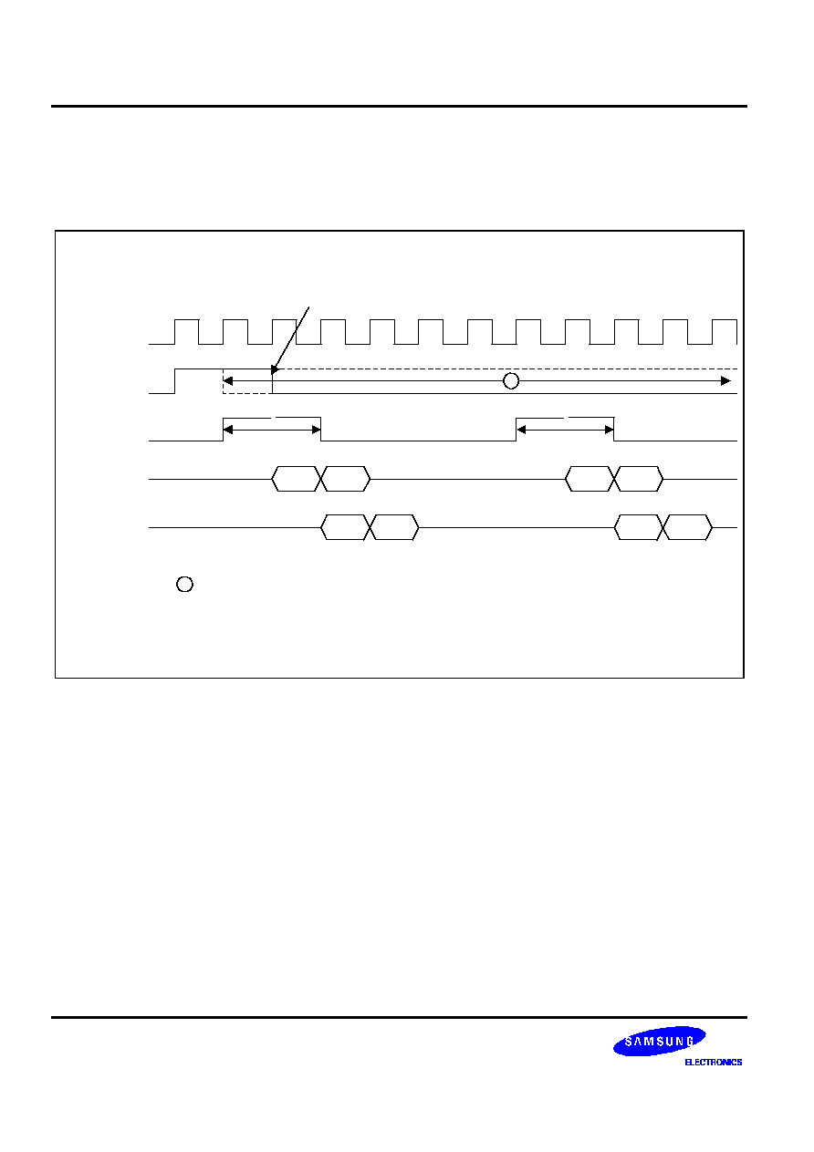
GDMA CONTROLLER
S3C2501X
9-22
9.6.3 BLOCK AND ONE DATA BURST MODE (DCON[3:1] = 001, [4] = 1, [5] = 0)
xGDMA_Req and xGDMA_Ack signals are active high.
GDMA transfers data from single xGDMA_Req signal till GDMA Transfer Count Register (DTCR) consumes to 0.
HCLK
xGDMA_Req
Recommand
deasserted time
xGDMA_Ack
Address
Data
NOTE:
' ' is in the block mode, GDMA starts to operate with first xGDMA_Req signal. So in the ideal case,
GDMA does not care the number of xGDMA_Req signal pulse. But I recommand that xGDMA_Req
siganl is deasserted when xGDMA_Ack signal is active state.
SA0
DA0
SD0
DD0
SA1
DA1
SD1
DD1
Programmable by
DCON[16:13]
Programmable by
DCON[16:13]
~ ~
~ ~
a
a
Figure 9-13. Block and One Data Burst Mode Timing

S3C2501X
GDMA CONTROLLER
9-23
9.6.4 BLOCK AND FOUR DATA BURST (DCON[3:1] = 001, [4] = 1, [5] = 1)
This timing diagram is the same with block and one data burst, except that it is four data burst.
HCLK
xGDMA_Req
Recommand
deasserted time
xGDMA_Ack
Address
Data
NOTE:
' ' is in the block mode, GDMA starts to operate with first xGDMA_Req signal. So in the ideal case,
GDMA does not care the number of xGDMA_Req signal pulse. But I recommand that xGDMA_Req
siganl is deasserted when xGDMA_Ack signal is active state.
Programmable by
DCON[16:13]
~ ~
a
SA2
SA3
SA1
SA0
DA0
DA1
DA2
DA3
SD2
SD3
SD1
SD0
DD0
DD1
DD2
DD3
a
Figure 9-14. Block and Four Data Burst Timing
one data burst; source address0 and source data0
destination address0 and destination data0
....
four data burst; source address0 and source data0
source address1 and source data1
source address2
and source data2
source address3 and source data3
destination address0 and destination
data0
destination address1 and destination data1
destination address2 and destination
data2
destination address3 and destination data3
source address4 and source data4
...
NOTE
In four data burst mode, GDMA transfers four data and GDMA Transfer Count Register (DTCR) value
decreases by four.

GDMA CONTROLLER
S3C2501X
9-24
NOTES

S3C2501X
SERIAL I/O (CONSOLE UART)
10-1
10
SERIAL I/O (CONSOLE UART)
10.1 OVERVIEW
The S3C2501X Console UART (Universal Asynchronous Receiver/Transmitter) unit provides one independent
asynchronous serial I/O (SIO) port. The port can operate in interrupt-based mode. That is, the Console UART can
generate internal interrupts to transfer data between the CPU and the serial I/O port.
10.2 FEATURES
The most important features of the S3C2501X Console UART include:
∑
Programmable baud rates
∑
Console UART source clock selectable (Internal clock: PCLK2, External clock: EXT_UCLK)
∑
(PCLK2 = PCLK / 2)
∑
Infra-red (IR) transmit/receive
∑
Insertion of one or two Stop bits per frame
∑
Selectable 5-bit, 6-bit, 7-bit, or 8-bit data transfers
∑
Parity checking
SIO unit has a baud rate generator, transmitter, receiver, and a control unit, as shown in Figure 10-1. The baud-
rate generator can be driven by the internal system clock, PCLK2, or by the external clock, EXT_UCLK. The
transmitter and receiver blocks have independent data registers and shifters.
Transmit data is written first to the transmit data register. From there, it is copied to the transmit shifter and then
shifted out by the transmit data pin, CUTXD. Receive data is shifted in by the receive data pin, CURXD. It is then
copied from the shifter to the receive data register when one data byte has been received.
The SIO control unit provides software controls for mode selection, and for status and interrupt generation. In
S3C2501X, software flow control can be selected according to the application.
The SIO control unit supports echo mode. Received data from CURXD send to not only CURXBUF but also
CUTXD. This mode is for test only.

SERIAL I/O (CONSOLE UART)
S3C2501X
10-2
S
Y
S
T
E
M
B
U
S
Control Character1,2
(CUCHAR1,2)
UART Status Register
(CUSTAT)
UART Interrupt Enable
(CUINT)
UART Control Register
(CUCON)
Transmit Shift Register
Transmit Data Register
(CUTXBUF)
Receive Shift Register
Receive Data Register
(CURXBUF)
IR Rx
Decoder
CURXD
0
1
IR Tx
Decoder
0
1
Baud Rate Divisor
Baud Rate Generator
CUTXD
Figure 10-1. Console UART Block Diagram

S3C2501X
SERIAL I/O (CONSOLE UART)
10-3
10.3 CONSOLE UART SPECIAL REGISTERS
Table 10-1. Console UART Special Registers Overview
Register
Address
R/W
Description
Size
Reset Value
CUCON
0xF0060000
R/W
Console UART control register
W
0x00000000
CUSTAT
0xF0060004
R/W
Console UART status register
W
0x00060800
CUINT
0xF0060008
R/W
Console UART interrupt enable register
W
0x00000000
CUTXBUF
0xF006000C
W
Console UART transmit data register
B
≠
CURXBUF
0xF0060010
R
Console UART receive data register
B
≠
CUBRD
0xF0060014
R/W
Console UART baud rate divisor register
H
0x0000
CUCHAR1
0xF0060018
R/W
Console UART control character register 1
W
0x00000000
CUCHAR2
0xF006001C
R/W
Console UART control character register 2
W
0x00000000

SERIAL I/O (CONSOLE UART)
S3C2501X
10-4
10.3.1 CONSOLE UART CONTROL REGISTERS
Table 10-2. CUCON Registers
Register
Address
R/W
Description
Size
Reset Value
CUCON
0xF0060000
R/W
Console UART control register
W
0x00000000
Table 10-3. Console UART Control Register Description
Bit Number
Bit Name
Description
[1:0]
Transmit mode
(TMODE)
This two-bit value determine which function is currently able to write
TX data to the Console UART transmit data register, CUTXBUF.
00 = Disable TX mode 01 = CPU request
10 = Reserved 11 = Reserved
[3:2]
Receive mode (RMODE) This two-bit value determine which function is currently able to read
RX data from the Console UART receive data register, CURXBUF.
NOTE: Changing these bits (TMODE, RMODE) while
transmitting/receiving cause abnormal UART operation. To
prevent Tx/Rx data from being lost, changing these bits while
transmitting/receiving is strictly prohibited.
00 = Disable RX mode 01 = CPU request
10 = Reserved 11 = Reserved
[4]
Send Break (SBR)
Set this bit to one to cause the Console UART to send a break. If
this bit value is zero, a break does not send. A break is defined as a
continuous Low level signal on the transmit data output with the
duration of more than one frame transmission time.
[5]
Serial Clock Select
(SCSEL)
This select bit specifies the clock source
0 = Internal (PCLK2)
1 = External (EXT_UCLK)
[6]
Reserved
Reserved
[7]
Loop-back mode
(LOOPB)
Setting this bit causes the Console UART to enter Loop-back mode.
In Loop-back mode, the transmit data output, CUTXD, keeps '1' and
the transmit data register, CUTXBUF, is internally connected to the
receive data register, CURXBUF.
NOTE: This mode is provided for test purposes only. For normal
operation, this bit should always be '0'.
[10:8]
Parity mode (PMD)
The 3-bit parity mode value specifies how parity generation and
checking are performed during Console UART transmit and receive
operations:
0xx = No parity 100 = Odd parity 101 = Even parity
110 = Parity is forced/checked as a '1'
111 = Parity forced/checked as a '0'
[11]
Number of Stop bits
(STB)
This bit specifies how many stop bits are used to signal end-of-
frame (EOF):
0 = One stop bit per frame 1 = Two stop bit per frame

S3C2501X
SERIAL I/O (CONSOLE UART)
10-5
Table 10-3. Console UART Control Register Description (Continued)
Bit Number
Bit Name
Description
[13:12]
Word Length (WL)
This two bit word length value indicates the number of data bits to
be transmitted or received per frame:
00 = 5bits 01 = 6bits 10 = 7bits 11 = 8bits
[14]
Infra-red mode (IR)
The S3C2501X Console UART block supports infra-red (IR)
transmit and receive operations. In IR mode, the transmit period is
pulsed at a rate of 3/16 that of the normal serial transmit rate
(when the transmit data value in the CUTXBUF register is zero).
To enable IR mode operation, you set CUCON[14] to '1'.
Otherwise, the Console UART operates in normal mode. In IR
receive mode, the receiver must detect the 3/16 pulsed period to
recognize a zero value in the receiver data register, CURXBUF, as
the IR receive data.
When this bit is '0', normal Console UART mode is selected. When
it is '1', infra-red TX/RX mode is selected.
NOTE: Changing this bit while tranmitting cause one Tx data losing.
Because level of infra-red frame start bit and idle state of
normal frame are identically high.
[28:15]
Reserved
Reserved
[29]
Software Flow Control
Enable (SFEN)
This bit determines whether Console UART select software flow
control or not. If you set CUCON[29] to '1', Console UART will act
in software flow control.
In this mode, you have to use Control Character register.
[30]
Echo Mode Enable
(ECHO)
If you set CUCON[30] to '1', RX data is sent not only CURXBUF
but also TX port directly, so CUTXBUF data will not be transmitted.
[31]
Reserved
Reserved

SERIAL I/O (CONSOLE UART)
S3C2501X
10-6
W
L
P
M
D
L
O
O
P
B
S
T
B
R
M
O
D
E
T
M
O
D
E
I
R
S
F
E
N
31
0
3
4
5
1
2
30 29 28 27 26 25
23 22
20 19
15 14
10
24
21
18 17 16
13 12 11
8
7
6
E
C
H
O
S
C
S
E
L
S
B
R
[1:0] SIO transmit mode selection (TMODE)
00 = Disable
01 = CPU request
10 = Reserved
11 = Reserved
[3:2] SIO receive mode selection (RMODE)
00 = Disable
01 = CPU request
10 = Reserved
11 = Reserved
[4] Send Break (SBR)
0 = Send normal TxData
1 = Send break signal
[5] Serial Clock Select (SCSEL)
0 = Internal (PCLK2)
1 = External (EXT_UCLK)
[6] Reserved (This bit should be cleared)
[7] Loopback Mode (LOOPB)
0 = Normal operating mode.
1 = Enable Loopback mode (only for test)
[10:8] Parity Mode (PMD)
0xx = No parity.
100 = Odd parity.
101 = Even parity.
110 = Parity forced/checked as 1
111 = Parity forced/checked as 0
[11] Stop Bits (STB)
0 = 1 stop bit
1 = 2 stop bits.
[13:12] Word Length (WL)
00 = 5-bit
01 = 6-bit
10 = 7-bit
11 = 8-bit
[14] Infra-red mode (IR)
0 = Normal operating mode
1 = Infra-red Tx/Rx mode
Figure 10-2. Console UART Control Register

S3C2501X
SERIAL I/O (CONSOLE UART)
10-7
S
B
R
W
L
P
M
D
L
O
O
P
B
S
T
B
R
M
O
D
E
T
M
O
D
E
I
R
S
F
E
N
31
0
3
4
5
1
2
30 29 28
26 25
23 22
20 19
15 14
10
24
21
18 17 16
13 12 11
8
7
6
E
C
H
O
S
C
S
E
L
[28:15] Reserved (This bit should be cleared)
[29] Software Flow Control Enable (SFEN)
0 = Disable Software Flow Control
1 = Enable Software Flow Control
[30] Echo Test Enable (ECHO)
0 = Disable Echo Test
1 = Enable Echo Test
[31] Reserved (This bit should be cleared)
Figure 10-3. Console UART Control Register

SERIAL I/O (CONSOLE UART)
S3C2501X
10-8
10.3.2 CONSOLE UART STATUS REGISTERS
Table 10-4. CUSTAT Registers
Register
Address
R/W
Description
Size
Reset Value
CUSTAT
0xF0060004
R/W
Console UART status register
W
0x00060800
Table 10-5. Console UART Status Register Description
Bit Number
Bit Name
Description
[0]
Receive Data Valid
(RDV)
This bit is automatically set to one when CURXBUF contains a valid
data received over the serial port. The received data can be read
from CURXBUF. When this bit is '0', there is no valid data.
If you set CUCON[3:2] to 2'b01 and CUINT[0] to 1'b1, the RDV
interrupt is requested. You can clear this bit by reading CURXBUF.
[1]
Break Signal Detected
(BKD)
This bit is automatically set to one to indicate that a break signal
has been received in CURXBUF.
If the BSD interrupt enable bit, CUINT[1], is '1', a interrupt is
generated when a break occurs.
You can clear this bit by writing '1' to this bit.
[2]
Frame Error (FER)
This bit is automatically set to '1' whenever a frame error occurs
during a serial data receive operation. A frame error occurs when a
zero is detected instead of the stop bit(s).
If the FER interrupt enable bit, CUINT[2], is '1' a interrupt is
generated when a frame error occurs.
You can clear this bit by writing '1' to this bit.
[3]
Parity Error (PER)
This bit is automatically set to '1' whenever a parity error occurs
during a serial data receive operation. If the PER interrupt enable
bit, CUINT[3], is '1', a interrupt is generated when a parity error
occurs.
You can clear this bit by writing '1' to this bit.

S3C2501X
SERIAL I/O (CONSOLE UART)
10-9
Table 10-5. Console UART Status Register Description (Continued)
Bit Number
Bit Name
Description
[4]
Overrun Error (OER)
This bit is automatically set to '1' whenever an overrun error occurs
during a serial data receive operation. When CURXBUF has a
previous valid data and a new received data is going to be written
into CURXBUF, CUSTAT[4] is set to '1'.
If the OER interrupt enable bit, CUINT[4], is '1', a interrupt is
generated when a overrun error occurs.
You can clear this bit by writing '1' to this bit.
[5]
Control Character Detect
(CCD)
CUSTAT[5] is automatically set to '1' to indicate that a control
character has been received.
If the CCD interrupt enable bit, CUINT[5], is '1', an interrupt is
generated when a control character is detected.
You can clear this bit by writing '1' to this bit.
NOTE: Software Flow Control mode does not affects Tx/Rx operation
this bit. This bit informs only whether UART receives control
character or not. Namely, if user want to stop Tx/Rx operation.
User must program that routine.
[10:6]
Reserved
Reserved
[11]
Receiver in idle
(RXIDLE)
This bit is only for CPU to monitor the receiver state of console
UART. The RXIDLE status bit indicates that the inactive state of
CURXBUF.
[16:12]
Reserved
[17]
Transmitter Idle (TI)
CUSTAT[17] is automatically set to '1' when the transmit holding
register has no valid data to transmit and when the TX shift register
is empty. The reset value is '1'
[18]
Transmit Holding
Register Empty (THE)
When CUTXBUF is empty without regarding TX shift register , this
bit set to '1'.
An interrupt is generated when CUSTAT[18] is '1', CUCON[1:0] is
'01', and CUINT[18] is '1'.
You can clear this bit by writing some data into CUTXBUF.
[31:19]
Reserved
Reserved

SERIAL I/O (CONSOLE UART)
S3C2501X
10-10
[0] Receive Data Valid (RDV)
0 = No valid data (Receive FIFO top or CURXBUF)
1 = Valid data present (Receive FIFO top or CURXBUF)
[1] Break Signal Deteced (BKD)
0 = No Break Signal (Receive FIFO top or CURXBUF)
1 = Break received
[2] Frame Error (FER)
0 = No Frame Error (Receive FIFO top or CURXBUF)
1 = Frame Error occured
[3] Parity Error (PER)
0 = No Frame Error (Receive FIFO top or CURXBUF)
1 = Parity Error occured
[4] Overrun Error (OER)
0 = No Overrun Error (Receive FIFO top or CURXBUF)
1 = Overrun Error occured
[5] Control Character Detect (CCD)
0 = No Control Character (Receive FIFO top or CURXBUF)
1 = Control character present (Receive FIFO top or CURXBUF)
[10:6] Reserved
[11] Receiver in IDLE (IDLE)
0 = Receiver is in active state
1 = Receiver is in IDLE state
[16:12] Reserved
[17] Transmitter Idle (TI)
0 = Transmit is in progress
1 = Transmitter is in idle: no data for Tx
[18] Transmit Holding Register Empty (THE)
0 = Tranmit holding register is not empty
1 = Transmit holding register is empty
[31:19] Reserved
C
C
D
O
E
R
T
H
E
T
I
I
D
L
E
F
E
R
R
D
V
B
K
D
P
E
R
31
0
3
4
5
1
2
19
10
18 17 16
12 11
6
Figure 10-4. Console UART Status Register

S3C2501X
SERIAL I/O (CONSOLE UART)
10-11
10.3.3 CONSOLE UART INTERRUPT ENABLE REGISTER
Table 10-6. CUINT Registers
Register
Address
R/W
Description
Size
Reset Value
CUINT
0xF0060008
R/W
Console UART interrupt enable register
W
0x00000000
Table 10-7. Console UART Interrupt Enable Register Description
Bit Number
Bit Name
Description
[0]
RDVIE
Receive Data Valid interrupt enable
[1]
BKDIE
Break Signal Detected interrupt enable
[2]
FERIE
Frame Error interrupt enable
[3]
PERIE
Parity Error interrupt enable
[4]
OERIE
Overrun Error interrupt enable
[5]
CCDIE
Control Character Detect interrupt enable
[16:6]
Reserved
[17]
TIIE
Transmitter Idle interrupt enable
[18]
THEIE
Transmit Holding Register Empty interrupt enable
[31:19]
Reserved

SERIAL I/O (CONSOLE UART)
S3C2501X
10-12
[0] Receive Data Valid Interrupt Enable (RDVIE)
[1] Break Signal Detected Interrupt Enable (BKDIE)
[2] Frame Error Interrupt Enable (FERIE)
[3] Parity Error Interrupt Enable (PERIE)
[4] Overrun Error Interrupt Enable (OERIE)
[5] Control Character Detect Interrupt Enable (CCDIE)
[16:6] Reserved
[17] Transmitter Idle (TIIE)
[18] Transmit Holding Register Empty Interrupt Enable (THEIE)
[31:19] Reserved
C
C
D
I
E
O
E
R
I
E
T
H
E
I
E
T
I
I
E
F
E
R
I
E
R
D
V
I
E
B
K
D
I
E
P
E
R
I
E
31
0
3
4
5
1
2
19 18 17 16
6
Figure 10-5. Console UART Interrupt Enable Register

S3C2501X
SERIAL I/O (CONSOLE UART)
10-13
10.3.4 UART TRANSMIT DATA REGISTER
Table 10-8. CUTXBUF Registers
Register
Address
R/W
Description
Size
Reset Value
CUTXBUF
0xF006000C
W
Console UART transmit data register
B
≠
Table 10-9. Console UART Transmit Register Description
Bit Number
Bit Name
Description
[7:0]
Transmit data
This field contains the data to be transmitted over the single
channel Console UART.
When this register is written, the transmit data register empty bit in
the status register, CUSTAT[18], should be `1'. This is to prevent
overwriting of transmit data that may already be present in the
CUTXBUF.
Whenever the CUTXBUF is written with a new value, the transmit
register empty bit, CUSTAT[18], is automatically cleared to `0'.
31
[7:0] Transmit data for UART
Transmit Data
0
7
8
Figure 10-6. Console UART Transmit Data Register

SERIAL I/O (CONSOLE UART)
S3C2501X
10-14
10.3.5 UART RECEIVE DATA REGISTER
Table 10-10. CURXBUF Registers
Register
Address
R/W
Description
Size
Reset Value
CURXBUF
0xF0060010
R
Console UART receive data register
B
≠
Table 10-11. Console UART Receive Register Description
Bit Number
Bit Name
Description
[7:0]
Receive data
This field contains the data received over the single channel
Console UART. When the Console UART finishes receiving a data
frame, the receive data ready bit in the Console UART status
register, CUSTAT[0], should be `1'. This prevents reading invalid
receive data that may already be present in the CURXBUF.
Whenever the CURXBUF is read, the receive data valid
bit(CUSTAT[0]) is automatically cleared to `0'.
31
[7:0] Receive data for UART
Receive Data
0
7
8
Figure 10-7. Console UART Receive Data Register

S3C2501X
SERIAL I/O (CONSOLE UART)
10-15
10.3.6 UART BAUD RATE DIVISOR REGISTER
The values stored in the baud rate divisor registers, CUBRD, let you determine the serial TX/RX clock rate (baud
rate) as follows:
BRGOUT =
PCLK2 or EXT_UCLK
(CNT0+1)
◊
16
CNT1
◊
16
Table 10-12. CUBRD Registers
Register
Address
R/W
Description
Size
Reset Value
CUBRD
0xF0060014
R/W
Console UART baud rate divisor register
H
0x0000
[3:0] Baud rate divisor value CNT1
xxx0 = Divide by 1
xxx1 = Divide by 16
[15:4] Time constant value for CNT0
31
15
16
0
18 17
19
21 20
22
23
24
25
26
27
28
29
30
CNT0
4 3
CNT1
Figure 10-8. Console UART Baud Rate Divisor Register

SERIAL I/O (CONSOLE UART)
S3C2501X
10-16
10.3.7 CONSOLE UART BAUD RATE EXAMPLES
If the system clock frequency is 133 MHz and PCLK2 is selected, the maximum BRGOUT output clock rate is
PCLK2/16 (= 4,156,250 Hz).
EXT_UCLK is the external clock input pin for Console UART. PCLK2 and EXT_UCLK can be selected by
CUCON[5] register.
Select
Clock
PCLK2
BRGOUT
EXT_UCLK
12-bit Counter
Divide by 1 or 16
Divide by 16
Sample Clock
CNT0
CNT1
NOTE:
CNT0 = CUBRD[15:4], CNT1 = CUBRD[3:0], Select Clock = CUCON[5]
Figure 10-9. Console UART Baud Rate Generator (BRG)
Table 10-13. Typical Baud Rates Examples of Console UART
Baud Rates
PCLK2 = 66.5 MHz
EXT_UCLK = 29.4912 MHz
(BRGOUT)
CNT0
(DEC/HEX)
CNT1
Freq.
Dev.(%)
CNT0
(DEC/HEX)
CNT1
Freq.
Dev.(%)
1200
3463/D87
0
1199.84
0.01
1535/5FF
0
1200.00
0.00
2400
1731/6C3
0
2399.68
0.01
767/2FF
0
2400.00
0.00
4800
865/361
0
4799.36
0.01
383/17F
0
4800.00
0.00
9600
432/1B0
0
9598.73
0.01
191/BF
0
9600.00
0.00
19200
215/D7
0
19241.90
0.01
95/5F
0
19200.00
0.00
38400
107/6B
0
38483.80
0.22
47/2F
0
38400.00
0.00
57600
71/47
0
57725.69
0.22
31/1F
0
57600.00
0.00
115200
35/23
0
115451.39
0.22
15/F
0
115200.00
0.00

S3C2501X
SERIAL I/O (CONSOLE UART)
10-17
10.3.8 UART CONTROL CHARACTER REGISTER 1 AND 2
These Control Character registers can be used for Software Flow control. In Software Flow Control mode, you
should write control characters into these registers. Any character in these registers can be used as a software
control flow character and you can use maximum 8 characters for it.
Table 10-14. CUCHAR 1, 2 Registers
Register
Address
R/W
Description
Size
Reset Value
CUCHAR1
0xF0060018
R/W
Console UART control character register 1
W
0x00000000
CUCHAR2
0xF006001C
R/W
Console UART control character register 2
W
0x00000000
31
15
16
[7:0] Control Character 0
[15:8] Control Character 1
[23:16] Control Character 2
[31:24] Control Character 3
CHAR0
0
24 23
7
8
CHAR1
CHAR3
CHAR2
Figure 10-10. Console UART Control Character 1 Register
31
15
16
[7:0] Control Character 4
[15:8] Control Character 5
[23:16] Control Character 6
[31:24] Control Character 7
CHAR4
0
24 23
7
8
CHAR5
CHAR7
CHAR6
Figure 10-11. Console UART Control Character 2 Register

SERIAL I/O (CONSOLE UART)
S3C2501X
10-18
<RECEIVE>
<TRANSMIT>
CURXBUF
INT_RXD
CURXD
INT_TXD
THE
CUTXD
Parity
Start
Data Bits (5-8)
Stop
(1-2)
Start
Parity
Data Bits (5-8)
Stop
(1-2)
Start
Start
Data Bits
Receive Data
Receive Data
Figure 10-12. Interrupt-Based Serial I/O Transmit and Receive Timing Diagram

S3C2501X
SERIAL I/O (CONSOLE UART)
10-19
0
1
0
1
0
0
1
1
0
1
Start
Bit
Stop
Bit
Data Bits
SIO Frame
Figure 10-13. Serial I/O Frame Timing Diagram (Normal Console UART)
0
1
0
1
0
0
1
1
0
1
Start
Bit
Stop
Bit
Data Bits
IR Transmit Frame
Bit frame = T
3/16T
7/16T 6/16T
Figure 10-14. Infra-Red Transmit Mode Frame Timing Diagram

SERIAL I/O (CONSOLE UART)
S3C2501X
10-20
0
1
0
1
0
0
1
1
0
1
Start
Bit
Stop
Bit
Data Bits
IR Receive Frame
Bit frame = T
3/16T
13/16T
Figure 10-15. Infra-Red Receive Mode Frame Timing Diagram

S3C2501X
SERIAL I/O (HIGH-SPEED UART)
11-1
11
SERIAL I/O (HIGH-SPEED UART)
11.1 OVERVIEW
The S3C2501X High-Speed UART (Universal Asynchronous Receiver/Transmitter) unit provides one
independent asynchronous serial I/O (SIO) ports. High-Speed UART can operate in interrupt-based or DMA-
based mode (DMA 3, 4, 5 for High-Speed UART channel). That is, the High-Speed UART can generate internal
interrupts or DMA requests to transfer data between the CPU and the serial I/O ports.
11.2 FEATURES
The most important features of the S3C2501X High-Speed UART include:
∑
Programmable baud rates
∑
32-byte Transmit FIFO and 32-byte Receive FIFO
∑
High-Speed UART source clock selectable (Internal clock: PCLK2, External clock : EXT_UCLK)
∑
(PCLK2 = PCLK / 2)
∑
Infra-red (IR) transmit/receive
∑
Insertion of one or two Stop bits per frame
∑
Selectable 5-bit, 6-bit, 7-bit, or 8-bit data transfers
∑
Parity checking
SIO unit has a baud rate generator, transmitter, receiver, and a control unit, as shown in Figure 11-1. The baud-
rate generator can be driven by the internal system clock divided by 2, PCLK2, or by the external clock,
EXT_UCLK. Auto Baud Rate Generator tries to get the baud rate from input data in this mode. The transmitter
and receiver blocks have independent data buffer registers and data shifters. And 32-byte transmit FIFO and 32-
byte receive FIFO is also provided which include transmit and receive buffer.
In non-FIFO mode, transmit data is written first to the transmit buffer register. From there, it is copied to the
transmit shifter and then shifted out by the transmit data pin, HUTXD. Receive data is shifted in by the receive
data pin, HURXD. It is then copied from the shifter to the receive buffer register when one data byte has been
received.
Otherwise, you can select FIFO mode. In FIFO mode, transmitter and receiver use transmit FIFO and receive
FIFO, instead of Tx/Rx buffer register(HUTXBUF/HURXBUF). They are controlled by each FIFO trigger level.
The SIO control units provide software controls for mode selection, and for status and interrupt generation.
In S3C2501X, software flow control or hardware flow control can be selected according to the application.

SERIAL I/O (HIGH-SPEED UART)
S3C2501X
11-2
Control
and
Status
Block
BaudRate Generator
and Detector
Modem Control Signal
TxBuffer Register
--------------
Transmit FIFO
(32 Bytes)
Transmit Shift
Register
RxBuffer Register
--------------
Receiver FIFO
(32 Bytes)
IR Tx Encoder
IR Rx Decoder
1
0
HUART
TX pin
HUART
RX pin
EXT_UCLK
Baud Rate
Divisor
Transmit Data
Receive Data
Transmit Control
Receive Control
Receive Status
Transmit Status
Control Character Register
PCLK2
HUCON: UCLK
HUCON: IR
S
Y
S
T
E
M
B
U
S
0
1
0
1
UART_CLK
Receiver Shift
Register
Figure 11-1. High-Speed UART Block Diagram

S3C2501X
SERIAL I/O (HIGH-SPEED UART)
11-3
11.3 HIGH-SPEED UART SPECIAL REGISTERS
Table 11-1. High-Speed UART Special Registers Overview
Register
Address
R/W
Description
Size
Reset Value
HUCON
0xF0080000
R/W
High-Speed UART control register
W
0x00000000
HUSTAT
0xF0080004
R/W
High-Speed UART status register
W
≠
HUINT
0xF0080008
R/W
High-Speed UART interrupt enable register
W
0x00000000
HUTXBUF
0xF008000C
W
High-Speed UART transmit data register
B
≠
HURXBUF
0xF0080010
R
High-Speed UART receive data register
B
≠
HUBRD
0xF0080014
R/W
High-Speed UART baud rate divisor register
H
0x00000000
HUCHAR1
0xF0080018
R/W
High-Speed UART control character register 1
W
0x00000000
HUCHAR2
0xF008001C
R/W
High-Speed UART control character register 2
W
0x00000000
HUABB
0xF0080020
R/W
High-Speed UART autobaud boundary register
W
0x170B0502
HUABT
0xF0080024
R/W
High-Speed UART autobaud table register
W
0x1F0F0703

SERIAL I/O (HIGH-SPEED UART)
S3C2501X
11-4
11.3.1 HIGH-SPEED UART CONTROL REGISTERS
Table 11-2. High-Speed UART Control Register
Registers
Address
R/W
Description
Reset Value
HUCON
0xF0080000
R/W
High-Speed UART control register
0x00000000
Table 11-3. High-Speed UART Control Register Description
Bit Number
Bit Name
Description
[1:0]
Transmit mode (TMODE) This two-bit value determines which function is currently able to write
Tx data to the High-Speed UART transmit buffer register, HUTXBUF.
00 = Disable Tx mode. 01 = Interrupt request
10 = GDMA request 11 = Reserved
(High-speed UART can use only GDMA 3,4,5 channel)
[3:2]
Receive mode (RMODE) This two-bit value determine which function is currently able to read
Rx data to the High-Speed UART receive buffer register, HURXBUF.
NOTE: Changing these bits (TMODE, RMODE) while
transmitting/receiving cause abnormal High-speed UART
operation. To prevent Tx/Rx data from being lost, changing these
bits while transmitting/receiving is strictly prohibited.
00 = Disable Rx mode. 01 = Interrupt request
10 = GDMA request 11 = Reserved
(High-speed UART can use only GDMA 3,4,5 channel)
[4]
Send Break (SBR)
Set this bit to one to cause the High-Speed UART to send a break. If
this bit value is zero, a break does not send. A break is defined as a
continuous Low level signal on the transmit data output with the
duration of more than one frame transmission time.
[5]
Serial Clock Selection
(UCLK)
This selection bit specifies the clock source.
0 = Internal (PCLK2)
1 = External (EXT_UCLK)
[6]
Auto Baud Rate Detect
(AUBD)
Setting this bit causes the High-Speed UART to enter Auto Baud
Rate Detect mode. In this mode, High-Speed UART try to get the
baud rate from input data. This bit automatically cleared when Auto
Baud Rate Detection procedure is successfully finished.
[7]
Loop-back mode
(LOOPB)
Setting this bit causes the High-Speed UART to enter Loop-back
mode. In Loop-back mode, the transmit data output is sent High level
and the transmit buffer register, HUTXBUF, is internally connected to
the receive buffer register, HURXBUF.
NOTE: This mode is provided for test purposes only.
For normal operation, this bit should always be "0".
[10:8]
Parity mode (PMD)
The 3-bit parity mode value specifies how parity generation and
checking are to be performed during High-Speed UART transmit and
receive operations.
0xx = no parity 100 = odd parity 101 = even parity
110 = parity is forced/checked as a "1"
111 = parity forced/checked as a "0"

S3C2501X
SERIAL I/O (HIGH-SPEED UART)
11-5
Table 11-3 High-Speed UART Control Register Description (Continued)
Bit Number
Bit Name
Description
[11]
Number of Stop bits
(STB)
This bit specifies how many stop bits are used to signal end-of-frame
(EOF).
0 = one stop bit per frame 1 = two stop bit per frame
[13:12]
Word Length (WL)
This two bit word length value indicates the number of data bits to be
transmitted or received per frame.
00 = 5-bit 01 = 6-bit 10 = 7-bit 11 = 8-bit
[14]
Infra-red mode (IR)
The S3C2501X High-Speed UART block supports infra-red (IR)
transmits and receives operations. In IR mode, the transmit period is
pulsed at a rate of 3/16 that of the normal serial transmit rate (when
the transmit data value in the HUTXBUF register is zero).
To enable IR mode operation, you set HUCON[14] to "1". Otherwise,
the High-Speed UART operates in normal mode. In IR receive mode,
the receiver must detect the 3/16 pulsed period to recognize a zero
value in the receiver buffer register, HURXBUF, as the IR receive
data.
When this bit is "0", normal High-Speed UART mode is selected.
When it is "1", infra-red Tx/Rx mode is selected.
NOTE: Changing this bit while tranmitting cause one Tx data losing.
Because level of infra-red frame start bit and idle state of
normal frame are identically high.
[15]
Reserved
This bit should be cleared by zero.
[16]
Transmit FIFO enable
(TFEN)
S3C2501X High-Speed UART block support 32-byte FIFO. If this bit
set to one, transmit data moved to Tx FIFO and then sent.
[17]
Receive FIFO enable
(RFEN)
S3C2501X High-Speed UART block support 32-byte FIFO. If this bit
set to one, receive data moved to Rx FIFO.
NOTE: Changing these bits (TFEN, RFEN) while transmitting/receiving
sending/receiving unexpected data. To prevent this, changing
these bits while transmitting/receiving is strictly prohibited.
[18]
Transmit FIFO reset
(TFRST)
You set this bit to '1', transmit FIFO will be reset. In this case, if there
is data in transmit shift register, it will be sent.
NOTE: This bit will not cleared automatically.
[19]
Receive FIFO reset
(RFRST)
You set this bit to '1', receive FIFO will be reset. In this case, if there is
data in receive shift register, it will be received.
NOTE: This bit will not cleared automatically.
[21:20]
Transmit FIFO trigger
level (TFTL)
This two bit trigger level value determines when the transmitter start to
transmit data in 32-byte transmit FIFO.
00 = 30-byte empty/32-byte 01 = 24/32
10 = 16/32 11 = 8/32
[23:22]
Receive FIFO trigger
level (RFTL)
This two bit trigger level value determines when the receiver starts to
move the received data in 32-byte receive FIFO.
00 = 1-byte valid/32-byte 01 = 8/32
10 = 18/32 11 = 28/32
[24]
Data Terminal Ready
to pin (DTR)
This bit directly controls the HUnDTR pin. Setting this bit to one, the
HUnDTR pin goes to Low level. If you set this bit to zero, it goes High
level.

SERIAL I/O (HIGH-SPEED UART)
S3C2501X
11-6
Table 11-3. High-Speed UART Control Register Description (Continued)
Bit Number
Bit Name
Description
[25]
Request to Send to pin
(RTS)
This bit directly controls the High-Speed UART pin only when the
High-Speed UART is not hardware flow control mode. If this bit set
to one, High-Speed UART pin goes Low level. Otherwise, it remains
High level.
[27:26]
Reserved
This bit should be cleared by zero.
[28]
Hardware Flow Control
Enable (HFEN)
This bit determines whether High-Speed UART select hardware flow
control or not. If this bit set to one, High-Speed UART will control all
pins concerning to hardware flow control.
[29]
Software Flow Control
Enable (SFEN)
This bit determines whether High-Speed UART select software flow
control or not. If this bit set to one, High-Speed UART will act in
software flow control.
In this mode, you have to use Control Character register.
[30]
Echo Mode
(ECHO)
If this bit is set to one, RX data is sent not only HURXBUF but also
TX port directly, so HUTXBUF data will not be transmitted.
[31]
RTS/RTR selection
(RTS/RTR)
This selection bit determines output of HUnRTS0/HUnRTS1 pin
0 = RTS
1 = RTR
NOTE: In RxFIFO mode, RTR goes to '1' when RxFIFO is full,
In NonRxFIFO mode, RTR goes to '1' when RxBUF is not empty.

S3C2501X
SERIAL I/O (HIGH-SPEED UART)
11-7
[1:0] SIO transmit mode selection (TMODE)
00 = Disable
01 = Interrupt request
10 = GDMA request
11 = Reserved
[3:2] SIO receive mode selection (RMODE)
00 = Disable
01 = Interrupt request
10 = GDMA request
11 = Reserved
[4] Send Break (SBR)
0 = Send normal TxData
1 = Send Break signal
[5] Serial Clock Selection (SCSEL)
0 = Internal systen clock divided 2 (PCLK2)
1 = External UART clock (EXT_UCLK)
[6] Auto Baud Rate Detect (AUBD)
0 = Normal operating mode.
1 = Auto Baud Rate Detect mode
[7] Loopback mode (LOOPB)
0 = Normal operating mode.
1 = Enable Loopback mode (only for test)
[10:8] Parity mode (PMD)
0xx = No parity.
100 = Odd parity.
101 = Even parity.
110 = Parity forced/checked as 1
111 = Parity forced/checked as 0
[11] Stop Bits (STB)
0 = 1 stop bit
1 = 2 stop bits.
[13:12] Word Length (WL)
00 = 5-bit
01 = 6-bit
10 = 7-bit
11 = 8-bit
[14] Infra-red mode (IR)
0 = normal operating mode.
1 = Infra-red Tx/Rx mode
[15] Reserved (This bit should be cleared)
31
0
3
4
5
1
2
30 29 28 27 26 25
23 22
20 19
15 14
10
24
21
18 17 16
13 12 11
8
7
6
H
F
E
N
S
C
S
E
L
S
B
R
R
T
S
D
T
R
R
F
T
L
T
F
T
L
W
L
R
F
R
S
T
T
F
R
S
T
R
F
E
N
T
F
E
N
P
M
D
L
O
O
P
B
A
U
B
D
S
T
B
R
M
O
D
E
T
M
O
D
E
I
R
S
F
E
N
E
C
H
O
R
T
S
R
T
R
Figure 11-2. High-Speed UART Control Register

SERIAL I/O (HIGH-SPEED UART)
S3C2501X
11-8
[16] Transmit FIFO Enable (TFEN)
0 = Disable Transmit FIFO
1 = Enable Transmit FIFO
[17] Receive FIFO Enable (RFEN)
0 = Disable Receive FIFO
1 = Enable Receive FIFO
[18] Tranmit FIFO Reset (TFRST)
0 = Normal operation
1 = Reset Transmit FIFO
[19] Receive FIFO Reset (RFRST)
0 = Normal operation
1 = Reset Receive FIFO
[21:20] Transmit FIFO Trigger Level (TFTL)
00 = 30/32 byte data
01 = 24/32 byte data
10 = 16/32 byte data
11 = 8/32 byte data (empty Tx data / TxFIFO depth)
[23:22] Receive FIFO Trigger Level (RFTL)
00 = 1/32 byte data
01 = 8/32 byte data
10 = 18/32 byte data
11 = 28/32 byte data (valid Rx data / RxFIFO depth)
[24] Data Terminal Ready to pin (DTR)
0 = HUnDTR goes high level
1 = HUnDTR goes low level
[25] Request To Send to pin (RTS)
0 = HUnRTS goes high level
1 = HUnRTS goes low level
[27:26] Reserved (This bit should be cleared)
[28] Hardware Flow Control Enable (HFEN)
0 = Disable Hardware Flow Control
1 = Enable Hardware Flow Control
[29] Software Flow Control Enable (SFEN)
0 = Disable Software Flow Control
1 = Enable Software Flow Control
[30] Echo Mode (ECHO)
0 = Normal
1 = ECHO mode
[31] RTS/RTR selection (RTS/RTR)
0 = RTS
1 = RTR
H
F
E
N
S
C
S
E
L
S
B
R
R
T
S
D
T
R
R
F
T
L
T
F
T
L
W
L
R
F
R
S
T
T
F
R
S
T
R
F
E
N
T
F
E
N
P
M
D
L
O
O
P
B
A
U
B
D
S
T
B
R
M
O
D
E
T
M
O
D
E
I
R
S
F
E
N
31
0
3
4
5
1
2
30 29 28 27 26 25
23 22
20 19
15 14
10
24
21
18 17 16
13 12 11
8
7
6
E
C
H
O
R
T
S
R
T
R
Figure 11-2. High-Speed UART Control Register (Continued)

S3C2501X
SERIAL I/O (HIGH-SPEED UART)
11-9
11.3.2 HIGH-SPEED UART STATUS REGISTERS
Table 11-4. High-Speed UART Status Register
Registers
Offset Address
R/W
Description
Reset Value
HUSTAT
0xF0080004
R/W
High-Speed UART status register
≠
Table 11-5. High-Speed UART Status Register Description
Bit Number
Bit Name
Description
[0]
Receive Data Valid
(RDV)
This bit automatically set to one when Receive FIFO-top or
HURXBUF contains a valid data received over the serial port. The
received data can be read from Receive FIFO-top or HURXBUF .
When this bit is "0", there is no valid data.
According to the current setting of the High-Speed UART receive
mode bits, an interrupt or DMA request is generated when
HUSTAT[0]="1". In case of HUCON[3:2]="01" and
HUINT[0],interrupt requested, and HUCON[3:2]="10" or "11", DMA
request occurred.
You can clear this bit by reading Receive FIFO or HURXBUF.
NOTE: Whether Receive FIFO-top or HURXBUF depends on the
HUCON[17].
[1]
Break Signal Detected
(BKD)
This bit automatically set to one to indicate that a break signal has
been received in Receive FIFO-top or HURXBUF.
If the BSD interrupt enable bit, HUINT[1], is "1", a interrupt is
generated when a break occurs.
You can clear this bit by writing '1' to this bit.
[2]
Frame Error (FER)
This bit automatically set to "1" whenever a frame error occurs
during a serial data receives operation. A frame error occurs when a
zero is detected instead of the stop bit(s).
If the FER interrupt enable bit, HUINT[2], is "1", a interrupt is
generated when a frame error occurs.
You can clear this bit by writing '1' to this bit.
[3]
Parity Error (PER)
This bit automatically set to "1" whenever a parity error occurs
during a serial data receives operation. If the PER interrupt enable
bit, HUINT[3], is "1", a interrupt is generated when a parity error
occurs.
You can clear this bit by writing '1' to this bit.

SERIAL I/O (HIGH-SPEED UART)
S3C2501X
11-10
Table 11-5. High-Speed UART Status Register Description (Continued)
Bit Number
Bit Name
Description
[4]
Overrun Error (OER)
This bit automatically set to "1" whenever an overrun error occurs
during a serial data receives operation. When HURXBUF has a
previous valid data, but a new received data is going to be written
into HURXBUF during Non-FIFO mode and when a new received
data is going to be written into RXFIFO with FIFO full during FIFO
mode. HUSTAT[4] is set to "1".
If the OER interrupt enable bit, HUINT[4], is "1", a interrupt is
generated when a overrun error occurs.
You can clear this bit by writing "1" to this bit.
[5]
Control Character Detect
(CCD)
HUSTAT[5] is automatically set to "1" to indicate that a control
character has been received.
If the CCD interrupt enable bit, HUINT[5], is "1", an interrupt is
generated when a control character is detected.
You can clear this bit by writing "1" to this bit.
NOTE: Software Flow Control mode does not affects Tx/Tx operation this
bit . This bit informs only whether UART receives control
character or not. Namely, if user want to stop Tx/Rx operation.
User must program that routine.
[6]
Data carrier Detect Lost
(DCDL)
This bit set to 1, if HUnDCD pin is high at the time High-Speed UART
Receiver checks a newly received data whether the data is good
frame or not.
If the DCD interrupt enable bit, HUINT[6], is "1", a interrupt is
generated when a data carrier is detected.
This bit can be used for error check bit in hardware flow control
mode.
[7]
Receive FIFO Data
trigger level reach
(RFREA)
In Receive FIFO mode, this bit indicates Receive FIFO has valid
data and reaches Rx trigger level. So High-Speed UART request
DMA to move data in Receive FIFO. In non-FIFO mode, if
HURXBUF has a received data , this bit is set to '1' also,
An interrupt or DMA request is generated when HUSTAT[7]="1". In
case of HUCON[3:2]= "01" and HUINT[7]= "1",interrupt requested,
and HUCON[3:2]= "10" or "11", DMA request occurred.
You can clear this bit by reading Receive FIFO or HURXBUF with a
good data. If any error, this bit is cleared by writing "1" to
corresponding error bit in HUSTAT register.
[8]
Receive FIFO empty
(RFEMT)
This bit is only for CPU to monitor High-Speed UART. When Receive
FIFO is empty, this bit is set to "1". After reset, default value is "1".
[9]
Receive FIFO full
(RFFUL)
This bit is only for CPU to monitor High-Speed UART. When Receive
FIFO is full, this bit is set to '1'. After reset, default value is '0'
[10]
Receive FIFO overrun
(RFOV)
This bit is set to "1" when Receive FIFO overrun occurs during the
Receive FIFO mode.
You can clear this bit by writing "1" to this bit.
[11]
Receiver in idle (RIDLE)
This bit is only for CPU to monitor the receiver state of High-Speed
UART. The RxIDLE status bit indicates that the inactive state of
RxDATA.

S3C2501X
SERIAL I/O (HIGH-SPEED UART)
11-11
Table 11-5. High-Speed UART Status Register Description (Continued)
Bit Number
Bit Name
Description
[12]
Receive Event time out
(E_RxTO)
During Receive FIFO mode, if there is a valid data in HURXFIFO or
Receive FIFO within a promised time internal which is determined
according to WL(Word Length) , this bit is set to '1'. HURXFIFO is
for non-FIFO mode and Receive FIFO is for FIFO mode.
If the E_RxTO interrupt enable bit, HUINT[12], is "1", an interrupt is
generated when a receive event time out is detected and valid data
reside in HURXBUF or Receive FIFO. You can clear this bit by
writing '1' to this bit.
NOTE: Event time = WL*4 +12
This bit set to one when the Rx data resides in RxFIFO.
[13]
AutoBaud Rate
Detection (AUBDDN)
This bit is automatically set to "1" when High-Speed UART finishes
AutoBaud Rate Detection procedure. You can clear this bit by
writing "1" to this bit.
[14]
Data Set ready (DSR)
This bit is only for CPU to monitor High-Speed UART.
When HUnDSR level is low, this bit is set. And HUnDSR high, this
bit is cleared.
[15]
Clear To Send (CTS)
This bit is only for CPU to monitor High-Speed UART.
When HUnCTS level is low , this bit is set. And HUnCTS high, this
bit is cleared.
[16]
CTS Event occurred
(E_CTS)
This bit is set to '1' whenever HUnCTS level changed.
If the E_CTS interrupt enable bit, HUINT[16], is "1", a interrupt is
generated when a CTS event is occurred.
You can clear this bit by writing '1' to this bit.
[17]
Transmitter Idle (TI)
HUSTAT[17] is automatically set to `1' when the transmit holding
register has no valid data to transmit and when the TX shift register
is empty. The reset value is '1'
[18]
Transmit Holding
Register Empty (THE)
In Transmit FIFO mode, when Transmit FIFO is empty to trigger
level, this bit set to '1'.
In Non-FIFO mode, when HUTXBUF is empty without regarding Tx
shift register , this bit set to '1'.
An interrupt or DMA request is generated when HUSTAT[18] is "1".
In case of HUCON[1:0]='01' and HUINT[18]=1, an interrupt
requested, and HUCON[1:0]='10' or '11', DMA request occurred.
You can clear this bit by writing TxDATA into HUTXBUF or Transmit
FIFO.
[19]
Transmit FIFO Empty
(TFEMT)
This bit is only for CPU to monitor High-Speed UART.
When Transmit FIFO is empty, this bit is set to '1'.
After reset, default value is '1'
[20]
Transmit FIFO full
(TFFUL)
This bit is only for CPU to monitor High-Speed UART.
When Transmit FIFO is full, this bit is set to '1'.
After reset, default value is '0' .
[31:21]
Reserved
Not applicable.

SERIAL I/O (HIGH-SPEED UART)
S3C2501X
11-12
[0] Receive Data Valid (RDV)
0 = No valid data (Receive FIFO-top or HURXBUF)
1 = Valid data present (Receive FIFO-top or HURXBUF)
[1] Break Signal Deteced (BKD)
0 = No Break Signal (Receive FIFO-top or HURXBUF)
1 = Break received
[2] Frame Error (FER)
0 = No Frame Error (Receive FIFO-top or HURXBUF)
1 = Frame Error occured
[3] Parity Error (PER)
0 = No Frame Error (Receive FIFO-top or HURXBUF)
1 = Frame Error occured
[4] Overrun Error (OER)
0 = No Overrun Error (Receive FIFO-top or HURXBUF)
1 = Overrun Error occured
[5] Control Character Detect (CCD)
0 = No Control Character (Receive FIFO-top or HURXBUF)
1 = Control character present (Receive FIFO-top or HURXBUF)
[6] Data Carrier Detect Lost (DCDL)
0 = DCD pin is Low at the receiver checking time
1 = DCD pin is High at the receiver checking time
[7] Receive FIFO Data Trigger Level Reach (RFREA)
0 = No valid data in HURXBUF or Not reached to trigger level
1 = In RxFIFO mode, RxFIFO has valid data and reach trigger level
In non-FIFO mode, HURXBUF has valid data
[8] Receive FIFO Empty (RFEMT)
0 = Receive FIFO is not empty
1 = Receive FIFO is empty
[9] Receive FIFO Full (RFFUL)
0 = Receive FIFO is not full
1 = Receive FIFO is full
[10] Receive FIFO Overrun (RFOV)
0 = Receive FIFO is not occured
1 = Receive FIFO overrun occured
[11] Receiver in IDLE (IDLE)
0 = Receiver is in IDLE state
1 = Receiver is in active state
31
0
3
4
5
1
2
20 19
15 14
10 9
21
18 17 16
13 12 11
8
7
6
C
C
D
O
E
R
T
F
F
U
L
E
_
R
X
T
O
T
F
E
M
T
T
H
E
T
I
E
_
C
T
S
R
F
F
U
L
R
F
R
E
A
D
C
D
L
I
D
L
E
F
E
R
R
D
V
D
S
R
B
K
D
P
E
R
R
F
E
M
T
R
F
O
V
C
T
S
A
U
B
D
D
N
Figure 11-3. High-Speed UART Status Register

S3C2501X
SERIAL I/O (HIGH-SPEED UART)
11-13
[12] Receive Event Time out (E_RxTO)
0 = A promised time is not elapsed during receiving.
1 = Valid data in a promised time
NOTE: A promised time is determined according to
WL (Word Length): Promised time = 4*WL + 12)
[13] Auto Baud Rate Detection Done (AUBDDN)
0 = Before AutoBaud Rate Detection
1 = After AutoBaud Rate Detection
[14] Data Set Ready (DSR)
0 = DSR pin goes High
1 = DSR pin goes Low
[15] Clear To Send (CTS)
0 = CTS pin goes High
1 = CTS pin goes Low
[16] CTS event occured (E_CTS)
0 = CTS pin has changed.
1 = CTS pin keep it's level
[17] Transmitter Idle (TI)
0 = Transmit is in progress.
1 = Transmitter is in idle; no data for Tx
[18] Transmit Holding Register Empty (THE)
0 = TxFIFO at trigger level or tranmit holding register is not empty.
1 = In TxFIFO mode, TxFIFO at trigger level is empty.
In non-FIFO mode, transmit holding register is empty.
[19] Transmit FIFO Empty (TFEMT)
0 = Transmit FIFO is not empty
1 = Transmit FIFO is empty
[20] Transmit FIFO full (TFFUL)
0 = Transmit FIFO is not full
1 = Transmit FIFO is full
[31:21] Reserved
31
0
3
4
5
1
2
20 19
15 14
10 9
21
18 17 16
13 12 11
8 7 6
C
C
D
O
E
R
T
F
F
U
L
E
_
R
X
T
O
T
F
E
M
T
T
H
E
T
I
E
_
C
T
S
R
F
F
U
L
R
F
R
E
A
D
C
D
L
I
D
L
E
F
E
R
R
D
V
D
S
R
B
K
D
P
E
R
R
F
E
M
T
R
F
O
V
C
T
S
A
U
B
D
D
N
Figure 11-3. High-Speed UART Status Register (Continued)

SERIAL I/O (HIGH-SPEED UART)
S3C2501X
11-14
11.3.3 HIGH-SPEED UART INTERRUPT ENABLE REGISTER
Table 11-6. High-Speed UART Interrupt Enable Register
Registers
Offset Address
R/W
Description
Reset Value
HUINT
0xF0080008
R/W
High-Speed UART Interrupt Enable register
0x00
Table 11-7. High-Speed UART Interrupt Enable Register Description
Bit Number
Bit Name
Description
[0]
RDVIE
Receive Data Valid interrupt enable
[1]
BKDIE
Break Signal Detected interrupt enable
[2]
FERIE
Frame Error interrupt enable
[3]
PERIE
Parity Error interrupt enable
[4]
OERIE
Overrun Error interrupt enable
[5]
CCDIE
Control Character Detect interrupt enable
[6]
DCDLIE
DCD High at receiver checking time interrupt enable
[7]
RFREAIE
Receive FIFO Data trigger level reach interrupt enable
[9:8]
Reserved
[10]
OVFFIE
Receive FIFO overrun interrupt enable
[11]
Reserved
[12]
E_RxTOIE
Receive Event time out interrupt enable
[13]
AUBDDNIE
AutoBaud Rate Detection done interrupt enable
[15:14]
Reserved
[16]
E_CTSIE
CTS Event occurred interrupt enable
[17]
TIIE
Transmitter Idle interrupt enable
[18]
THEIE
Transmit Holding Register Empty interrupt enable
[31:19]
Reserved

S3C2501X
SERIAL I/O (HIGH-SPEED UART)
11-15
[0] Receive Data Valid Interrupt Enable (RDVIE)
[1] Break Signal Detected Interrupt Enable (BKDIE)
[2] Frame Error Interrupt Enable (FERIE)
[3] Parity Error Interrupt Enable (PERIE)
[4] Overrun error Interrupt Enable (OERIE)
[5] Control Character Detect Interrupt Enable (CCDIE)
[6] Data Carrier Detect Lost Interrupt Enable (DCDLIE)
[7] Receive FIFO Data Trigger Level Reach Interrupt Enable (RFREAIE)
[9:8] Reserved
[10] Receive FIFO overrun Interrupt Enable (OVFFIE)
[11] Reserved
[12] Receive Event Time out Interrupt Enable (E_RxTOIE)
[13] AutoBaud Rate Detection done interrupt enable (AUBDDNIE)
[15:14] Reserved
[16] CTS event occured Interrupt Enable (E_CTSIE)
[17] Transmitter Idle (TIIE)
[18] Transmit Holding Register Empty Interrupt Enable (THEIE)
This bit used in FIFO mode for interrupt enable when transmit
FIFO empty as much transmit data trigger level.
[31:19] Reserved
31
0
3
4
5
1
2
19
15
10 9
18 17 16
13 12 11
8 7 6
C
C
D
I
E
O
E
R
I
E
E
_
R
x
T
O
I
E
T
H
E
I
E
E
_
C
T
S
I
E
R
F
R
E
A
I
E
D
C
D
L
I
E
F
E
R
I
E
R
D
V
I
E
B
K
D
I
E
P
E
R
I
E
O
V
F
F
I
E
T
I
I
E
A
U
B
D
D
N
I
E
14
Figure 11-4. High-Speed UART Interrupt Enable Register

SERIAL I/O (HIGH-SPEED UART)
S3C2501X
11-16
11.3.4 HIGH-SPEED UART TRANSMIT BUFFER REGISTER
S3C2501X has a 32-byte Transmit FIFO, and the bottom of FIFO is HUTXBUF. All data to be transmitted are
stored into this register at first in FIFO mode, if next buffer has invalid data, then shifted to next buffer. But in
non-FIFO mode, a new data to transmit will be moved from HUTXBUF to Tx shift register. The High-Speed
UART transmit buffer registers, HUTXBUF, contain an 8-bit data value to be transmitted over the High-Speed
UART channel.
Table 11-8. High-Speed UART Transmit Register
Registers
Offset Address
R/W
Description
Reset Value
HUTXBUF
0xF008000C
W
High-Speed UART transmit buffer register
≠
Table 11-9. High-Speed UART Transmit Register Description
Bit Number
Bit Name
Description
[7:0]
Transmit data
This field contains the data to be transmitted over the single channel High-
Speed UART.
When this register is written, the transmit buffer register empty bit in the
status register, HUSTAT[18], should be "1". This is to prevent overwriting of
transmit data that may already be present in the HUTXBUF.
Whenever the HUTXBUF is written with a new value, the transmit register
empty bit, HUSTAT[18], is automatically cleared to "0".
31
[7:0] Transmit data for UART
Transmit Data
0
7
8
Figure 11-5. High-Speed UART Transmit Buffer Register

S3C2501X
SERIAL I/O (HIGH-SPEED UART)
11-17
11.3.5 HIGH-SPEED UART RECEIVE BUFFER REGISTER
S3C2501X has a 32-byte Receive FIFO, and the bottom of FIFO is HURXBUF. All data to be received are stored
in this register at first in FIFO mode, if next buffer has invalid data, then shifted to next buffer. But in Non-FIFO
mode, a new received data will be moved to HURXBUF. The High-Speed UART receive buffer registers,
HURXBUF contain an 8-bit data value to be received over the High-Speed UART channel.
Table 11-10. High-Speed UART Receive Register
Registers
Offset Address
R/W
Description
Reset Value
HURXBUF
0xF0080010
R
High-Speed UART receive buffer register
≠
Table 11-11. High-Speed UART Receive Register Description
Bit Number
Bit Name
Description
[7:0]
Receive data
This field contains the data received over the single channel High-Speed
UART. When the High-Speed UART finishes receiving a data frame, the
receive data ready bit in the High-Speed UART status register,
HUSTAT[14], should be "1". This prevents reading invalid receive data that
may already be present in the HURXBUF. Whenever the HURXBUF is read,
the receive data valid bit(HUSTAT[14]) is automatically cleared to "0".
31
[7:0] Receive data for UART
Receive Data
0
7
8
Figure 11-6. High-Speed UART Receive Buffer Register

SERIAL I/O (HIGH-SPEED UART)
S3C2501X
11-18
11.3.6 HIGH-SPEED UART BAUD RATE DIVISOR REGISTER
The values stored in the baud rate divisor registers, HUBRD let you determine the serial Tx/Rx clock rate (baud
rate) as follows:
BRGOUT =
PCLK2 or EXT_UCLK
(CNT0+1)
◊
16
CNT1
◊
16
Table 11-12. High-Speed UART Transmit Register
Registers
Offset Address
R/W
Description
Reset Value
HUBRD
0xF0080014
R/W
High-Speed UART baud rate divisor register
0x00
31
19
15
16
[3:0] Baud reate divisor value CNT1
xxx0 = divide by 1
xxx1 = divide by 16
[15:4] Time constant value for CNT0
CNT0
0
18 17
20
30 29 28 27 26 25 24 23 22 21
3
4
CNT1
Figure 11-7. High-Speed UART Baud Rate Divisor Register

S3C2501X
SERIAL I/O (HIGH-SPEED UART)
11-19
11.3.7 HIGH-SPEED UART BAUD RATE EXAMPLES
High-Speed UART BRG input clock, PCLK2 is the system clock frequency divided by 2.
If the system clock frequency is 133 MHz and PCLK2 is selected, the maximum BRGOUT output clock rate is
PCLK2/16 (= 4,156,250 Hz).
EXT_UCLK is the external clock input pin for High-Speed UART, PCLK2, EXT_UCLK can be selected by
HUCON[6] register.
Select Clock
PCLK2
BRGOUT
EXT_UCLK
12-bit Counter
Divide by 1 or 16
Divide by 16
Sample Clock
CNT0
CNT1
NOTE:
CNT0 = HUBRD[15:4], CNT1 = HUBRD[3:0], Select Clock = HUCON[6]
Figure 11-8. High-Speed UART Baud Rate Generator (BRG)
Table 11-13. Typical Baud Rates Examples of High-Speed UART
Baud Rates
PCLK2 = 66.5 MHz
EXT_UCLK = 29.4912 MHz
(BRGOUT)
CNT0
(DEC/HEX)
CNT1
Freq.
Dev.(%)
CNT0
(DEC/HEX)
CNT1
Freq.
Dev.(%)
1200
3463/D87
0
1199.84
0.01
1535/5FF
0
1200.00
0.00
2400
1731/6C3
0
2399.68
0.01
767/2FF
0
2400.00
0.00
4800
865/361
0
4799.36
0.01
383/17F
0
4800.00
0.00
9600
432/160
0
9598.73
0.01
191/BF
0
9600.00
0.00
19200
215/D7
0
19241.90
0.01
95/5F
0
19200.00
0.00
38400
107/6B
0
38483.80
0.22
47/2F
0
38400.00
0.00
57600
71/47
0
57725.69
0.22
31/1F
0
57600.00
0.00
115200
35/23
0
115451.39
0.22
15/F
0
115200.00
0.00
230400
17/11
0
230902.78
0.22
7/7
0
230400.00
0.00
460800
8/8
0
461805.56
0.22
3/3
0
460800.00
0.00
921600
4/4
0
831250.00
9.80
1/1
0
921600.00
0.00

SERIAL I/O (HIGH-SPEED UART)
S3C2501X
11-20
11.3.8 HIGH-SPEED UART CONTROL CHARACTER 1 REGISTER
This Control Character registers can be used for Software Flow control. In Software Flow Control mode, you
should write control characters into this registers. If not, the reset value will be used as control character. For
example, even if you want to use one control character, all control characters will have same value with it.
Table 11-14. High-Speed UART Control Charater 1 Register
Registers
Offset Address
R/W
Description
Reset Value
HUCHAR1
0xF0070018
R/W
High-Speed UART control character1 register
0x00
31
15
16
[7:0] Control Character 0
[15:8] Control Character 1
[23:16] Control Character 2
[31:24] Control Character 3
CONCHAR0
0
24 23
7
8
CONCHAR1
CONCHAR3
CONCHAR2
Figure 11-9. High-Speed UART Control Character 1 Register

S3C2501X
SERIAL I/O (HIGH-SPEED UART)
11-21
11.3.9 HIGH-SPEED UART CONTROL CHARACTER 2 REGISTER
This Control Character registers can be used for Software Flow control. In Software Flow Control mode, you
should write control characters into this registers. If not, the reset value will be used as control character. For
example, even if you want to use one control character, all control characters will have same value with it.
Table 11-15. High-Speed UART Control Character 2 Register
Registers
Offset Address
R/W
Description
Reset Value
HUCHAR2
0xF008001C
R/W
High-Speed UART control character2 register
0x00
31
15
16
[7:0] Control Character 4
[15:8] Control Character 5
[23:16] Control Character 6
[31:24] Control Character 7
CONCHAR4
0
24 23
7
8
CONCHAR5
CONCHAR7
CONCHAR6
Figure 11-10. High-Speed UART Control Character 2 Register

SERIAL I/O (HIGH-SPEED UART)
S3C2501X
11-22
11.3.10 HIGH-SPEED UART AUTOBAUD BOUNDARY REGISTER
This autobaud boundary register limit range of each baud rate value that is auto-detected. ABB0 is the lowest
boundary value (high baud rate) and ABB3 is the highest value (low baud rate) of autobaud boundary register
(actually the highest boundary value is ABT3). Refer figure 11-13 for detail range.
ABT3
ABB3
ABB1
ABT0
ABB0
~
~
~
.
.
.
.
.
ABT3
ABT0
Figure 11-11. AutoBaud Boundary Register Range
Table 11-16. High-Speed UART AutoBaud Boundary Register
Registers
Offset Address
R/W
Description
Reset Value
HUABB
0xF0080020
R/W
High-Speed UART autobaud boundary register
0x170B0502
31
15
16
[7:0] AutoBaud Boundary 0
[15:8] AutoBaud Boundary 1
[23:16] AutoBaud Boundary 2
[31:24] AutoBaud Boundary 3
ABB0
0
24 23
7
8
ABB1
ABB3
ABB2
Figure 11-12. High-Speed UART AutoBaud Boundary Register

S3C2501X
SERIAL I/O (HIGH-SPEED UART)
11-23
11.3.11 HIGH-SPEED UART AUTOBAUD TABLE REGSITER
This autobaud table register corrects each baud rate divisor value that is auto-detected. For detail refer figure 11-
15. If high-speed UART uses external UCLK (29.4912 MHz) and you want to use 460800 baud rate, though high-
speed UART detects baud rate divisor register value (CNT0, CNT1) as 0x04, autobaud mechanism will correct
baud rate divisor register value as 0x03, because detected value is between 0x05 (ABB1) and 0x02 (ABB0).
ABT0 is lowest table value and ABT3 is highest table value, also ABT3 is highest boundary value of total range.
If out of range value is detected, it will be written normally without modification.
If 0x1F was detected
Rewrite: 0x1F
If 0x0B was detected
If 0x04 was detected
Rewrite: 0x07
Rewrite: 0x03
ABT3
0x1F
ABB3
0x17
ABT2
0x0F
ABB2
0x0B
ABT1
0x07
ABB1
0x05
ABT0
0x03
ABB0
0x02
Figure 11-13. Example of AutoBaud Table Register Setting
Table 11-17. High-Speed UART AutoBaud Table Register
Registers
Offset Address
R/W
Description
Reset Value
HUABT
0xF0080024
R/W
High-Speed UART autobaud boundary register
0x1F0F0703
31
15
16
[7:0] AutoBaud Table 0
[15:8] AutoBaud Table 1
[23:16] AutoBaud Table 2
[31:24] AutoBaud Table 3
ABT0
0
24 23
7
8
ABT1
ABT3
ABT2
Figure 11-14. High-Speed UART AutoBaud Table Register

SERIAL I/O (HIGH-SPEED UART)
S3C2501X
11-24
11.4 HIGH-SPEED UART OPERATION
Data Transmit Operation Flow:
If there is no data at Tx Buffer FIFO of High-Speed UART (in case of FIFO, if data in the Tx FIFO are empty as
same amount of trigger level), High-Speed UART generates interrupt or GDMA request signal. It depends on
High-Speed UART mode. CPU(or software) or GDMA controller will read data from memory where High-Speed
UART transmit data are stored, and send them to Tx Buffer/FIFO. Transfer unit is byte. When data come from
High-Speed UART Rx pin, data are stored to Rx Buffer/FIFO, via shift register. If valid Rx data are received,
High-Speed UART generates interrupt or GDMA request signal. (Similar to Tx Block, in case of FIFO, it is same
as Tx block. Data should be stored as the same level of trigger level.) If there is an error on Rx data, High-Speed
UART does not generate GDMA request signal but generates interrupt even in case of GDMA mode.
(Although High-Speed UART is FIFO mode, if error data shift to FIFO top, then High-Speed UART generates
interrupt.) Transfer unit is byte, same as at Tx block.
11.4.1 FIFO OPERATION
Tx FIFO Operation:
If there is no valid data on trigger level of TX FIFO, High-Speed UART generates interrupt (INT_TXD) or sends a
request signal to GDMA. During this operation trigger level should be 30/32 (empty depth/FIFO depth), 24/32,
16/32 or 8/32. CPU or GDMA fills data into TX FIFO by byte.
Rx FIFO Operation:
If received data are filled up to RX FIFO trigger level, High-Speed UART generate interrupt (INT_RXD) or send
request signal to GDMA. The size of transferred data is 1 byte. If RX data contains error in case of GDMA mode
operation, High-Speed UART generates interrupt instead of sending request signal to GDMA. Then CPU
executes interrupt service routine for error data. So GDMA transmits (error free) valid data only from received
data.
11.4.2 HARDWARE FLOW CONTROL
Hardware Flow Control for Transmit Operation:
When CTS signal level is high during Transmit operation -
High-Speed UART transmits TX DATA to TX line normally.
When CTS signal level is low during Transmit operation -
If CTS signal level is low when High-Speed UART transmits TX DATA to TX line, High-Speed UART stops data
transmission immediately. In this case, transmitting TX data will be lost.
Hardware Flow Control for Receive Operation:
In the hardware flow control, during High-Speed UART receive data from Rx pin, DCD level have to be low. If
DCD level goes high, received data will be pull up by High-Speed UART Rx block from that time.

S3C2501X
SERIAL I/O (HIGH-SPEED UART)
11-25
Start Bit
Data Size
TXD
RTS
CTS
Figure 11-15. When CTS Signal Level is High During Transmit Operation
Start Bit
Data Region
TXD
RTS
CTS
Stop Bit
Figure 11-16. When CTS Signal Level is Low During Transmit Operation

SERIAL I/O (HIGH-SPEED UART)
S3C2501X
11-26
Start Bit
Data Region
RXD
RTS
CTS
Stop Bit
Figure 11-17. Normal Received Rx Data
Data Region
RXD
Pin Signal
DCD
RXD
Internal
Signal
Start Bit
Stop Bit
Start Bit
Figure 11-18. DCD Lost During Rx Data Receive
11.4.3 SOFTWARE FLOW CONTROL
Software can control High-Speed UART by control characters. High-Speed UART compares received data with
control characters, and if they are identical, it sets "1" at state bit (CCD:HUSTAT[5]) and generates interrupt
which masked by Interrupt enable register.
11.4.4 AUTO BAUD RATE DETECTION
To use Auto Baud Rate Detection, Set ABB(AutoBaud rate Boundary), ABT(AutoBaud rate Table) Register and
Auto Baud Detect bit(AUBD:HUCON[6]), When RXD level is low, High-Speed UART counts low-level of start
singal ( `A' ) and rewrites counting value of low-level by comparing ABB, ABT Register. This automatically
corrects Baud Rate(CNT0 and CNT1)

S3C2501X
SERIAL I/O (HIGH-SPEED UART)
11-27
<RECEIVE>
<TRANSMIT>
HURXBUF
INT_RXD
RX DATA
INT_TXD
THE
TX DATA
Parity
Start
Data Bits (5-8)
Stop
(1-2)
Start
Parity
Data Bits (5-8)
Stop
(1-2)
Start
Start
Data Bits
Receive Data
Receive Data
Figure 11-19. Interrupt-Based Serial I/O Transmit and Receive Timing Diagram

SERIAL I/O (HIGH-SPEED UART)
S3C2501X
11-28
<TRANSMITTER>
uart_tx_req
TX DATA
TMODE
Select DMA Mode
uart_tx_ack
Parity
Start
Data Bits (5-8)
Stop
(1-2)
Figure 11-20. DMA-Based Serial I/O Timing Diagram (Tx Only)
< RECEIVER >
HU_RXBUF
uart_rx_req
RX DATA
Previous Receive Data
Parity
Data Bits (5-8)
Stop
(1-2)
Start
Start
Data Bits
Valid Receive Data
RMODE
Select DMA Mode
uart_rx_ack
Figure 11-21. DMA-Based Serial I/O Timing Diagram (Rx Only)

S3C2501X
SERIAL I/O (HIGH-SPEED UART)
11-29
0
1
0
1
0
0
1
1
0
1
Start
Bit
Stop
Bit
Data Bits
SIO Frame
Figure 11-22. Serial I/O Frame Timing Diagram (Normal High-Speed UART)
0
1
0
1
0
0
1
1
0
1
Start
Bit
Stop
Bit
Data Bits
IR Transmit Frame
Bit frame = T
3/16T
7/16T 6/16T
Figure 11-23. Infra-Red Transmit Mode Frame Timing Diagram

SERIAL I/O (HIGH-SPEED UART)
S3C2501X
11-30
0
1
0
1
0
0
1
1
0
1
Start
Bit
Stop
Bit
Data Bits
IR Transmit Frame
Bit frame = T
3/16T
13/16T
Figure 11-24. Infra-Red Receive Mode Frame Timing Diagram

S3C2501X
I/O PORTS
12-1
12
I/O PORTS
12.1 OVERVIEW
S3C2501X has 64 programmable I/O ports. I/O port function control registers (IOPCON2: upper word, IOPCON1:
lower word) select either function's port or GPIO. If IOPCON1/2 register is set to GPIO, IOPMODE1/2 register
should be set to either input mode or output mode.
For example, if you select IOPCON1/2 for GPIO and IOPMODE1/2 for input, then I/O port can be used for GPIO
input mode. When the value is latched in IOPDATA1/2 register, CPU can read IOPDATA1/2 register value. If you
select IOPCON1/2 for GPIO and IOPMODE1/2 for output, then CPU can write the data to IOPDATA1/2 register
and the value can be transferred to the output port.
I/O Ports
= Pad Ports
(or PP)
Function's Port
GPIO
Input Mode
Output Mode
If you select IOPCON1[14] for xGDMA Req[0], then the port is used for GDMA Req port mode. I/O port signal
decision register (IOPGDMA) is used when IOPCON1 is selected for GDMA Req/Ack. IOPGDMA controls
external GDMA Req/Ack signals.
IOPEXTINTPND register is used for external interrupt status. IOPEXTINTPND is set when external interrupt is
generated and is cleared when IOPEXTINTPND register is re-written to '1'.
12.2 FEATURES
∑
64 Programmable I/O Ports
∑
Configurable to Input, Output, or I/O Mode for Dedicated Signals
∑
6 External Interrupt Requests
∑
4 External GDMA Requests
∑
4 External GDMA Acknowledges
∑
6 Timer Outputs
∑
7 UART Signals
NOTE
PP[27] - PP[18] ports support external software reset. When PP[27:18] are in GPIO output mode and
when nRESET or System Reset (including watchdog reset) is asserted, the external devices that are
connected to PP[27:18] are also reset. (That is, the output signals stay high, and fall back to low.)

I/O PORTS
S3C2501X
12-2
12.3 I/O PORT SPECIAL REGISTER
Table 12-1. I/O Port Special Registers
Register
Address
R/W
Description
Reset Value
IOPMODE1
0xF0030000
R/W
I/O port mode select register for port 0 to 31
0xF003FFFF
IOPMODE2
0xF0030004
R/W
I/O port mode select register for port 32 to 63
0xFFFFFFFF
IOPCON1
0xF0030008
R/W
I/O port function control register for port 0 to 31
0xFFFFFF00
IOPCON2
0xF003000C
R/W
I/O port function control register for port 32 to 63
0xFFFFFC07
IOPGDMA
0xF0030010
R/W
I/O port special function register for GDMA
0x00000000
IOPEXTINT
0xF0030014
R/W
I/O port special function register for external
interrupt
0x00000000
IOPEXTINT
PND
0xF0030018
R/W
I/O port external interrupt clear register
0x00000000
IOPDATA1
0xF003001C
R/W
I/O port data register for port 0 to 31
Undefined
IOPDATA2
0xF0030020
R/W
I/O port data register for port 32 to 63
Undefined
IOPDRV1
0xF0030024
R/W
I/O port drive control register for port 0 to 31
0x00000000
IOPDRV2
0xF0030028
R/W
I/O port drive control register for port 32 to 63
0x00000000
12.3.1 I/O PORT MODE SELECT REGISTER (IOPMODE1/2)
If you set IOPCON1/2 registers to GPIO, then IOPMODE1/2 registers should determine whether input or output
mode for each port.
Table 12-2. IOPMODE1/2 Registers
Register
Address
R/W
Description
Reset Value
IOPMODE1
0xF0030000
R/W
I/O port mode select register for port 0 to 31
0xF003FFFF
IOPMODE2
0xF0030004
R/W
I/O port mode select register for port 32 to 63
0xFFFFFFFF

S3C2501X
I/O PORTS
12-3
31
X
0
12
13
14
9
10
11
6
7
8
3
4
5
1
2
X
X
X
X
X
X
15
16
17
18
19
20
21
22
23
24
25
26
27
28
29
30
X
X
X
X
X
X
X
X
X
X
X
X
X
X
X X
X
IOPMODE1
X X X X X
X
X
X
31
X
0
12
13
14
9
10
11
6
7
8
3
4
5
1
2
X
X
X
X
X
X
15
16
17
18
19
20
21
22
23
24
25
26
27
28
29
30
X
X
X
X
X
X
X
X
X
X
X
X
X
X
X X
X
IOPMODE2
X X X X X
X
X
X
Signal port
Bit
NOTE: IOPMODE1/2 registers bit value 1 is input mode, bit value 0 is output mode.
IOPMODE1
Reset value
GPIO[31]
GPIO[30]
GPIO[29]
GPIO[28]
GPIO[27]
GPIO[26]
GPIO[25]
GPIO[24]
GPIO[23]
GPIO[22]
GPIO[21]
GPIO[20]
GPIO[19]
GPIO[18]
GPIO[17]
GPIO[16]
GPIO[15]
GPIO[14]
GPIO[13]
GPIO[12]
GPIO[11]
GPIO[10]
GPIO[9]
GPIO[8]
GPIO[7]
GPIO[6]
GPIO[5]
GPIO[4]
GPIO[3]
GPIO[2]
GPIO[1]
GPIO[0]
1
1
1
1
0
0
0
0
0
0
0
0
0
0
1
1
1
1
1
1
1
1
1
1
1
1
1
1
1
1
1
1
GPIO[63]
GPIO[62]
GPIO[61]
GPIO[60]
GPIO[59]
GPIO[58]
GPIO[57]
GPIO[56]
GPIO[55]
GPIO[54]
GPIO[53]
GPIO[52]
GPIO[51]
GPIO[50]
GPIO[49]
GPIO[48]
GPIO[47]
GPIO[46]
GPIO[45]
GPIO[44]
GPIO[43]
GPIO[42]
GPIO[41]
GPIO[40]
GPIO[39]
GPIO[38]
GPIO[37]
GPIO[36]
GPIO[35]
GPIO[34]
GPIO[33]
GPIO[32]
1
1
1
1
1
1
1
1
1
1
1
1
1
1
1
1
1
1
1
1
1
1
1
1
1
1
1
1
1
1
1
1
Signal port
IOPMODE2
Reset value
31
30
29
28
27
26
25
24
23
22
21
20
19
18
17
16
15
14
13
12
11
10
9
8
7
6
5
4
3
2
1
0
See NOTE on
Page 12-1.
Figure 12-1. I/O Port Mode Registers 1/2 (IOPMODE1/2)

I/O PORTS
S3C2501X
12-4
12.3.2 I/O PORT FUNCTION CONTROL REGISTER (IOPCON1/2)
The I/O port function select registers, IOPCON1/2, are used for function select. IOPCON1/2 are used to
configure external interrupt signals, GDMA Req/Ack signals, timer signals and UART Tx/Rx signals. For
example, if you set IOPCON1[14] to '0', then port14 is used for GDMA Req port. If you set the IOPGDMA[14] to
`1', then port14 is used for GPIO.
NOTE
If the port is used for a function's port such as an external interrupt request or an external GDMA
Req/Ack signal, its signal function is determined by IOPGDMA or IOPEXTINT register.
Table 12-3. IOPCON1/2 Register
Register
Address
R/W
Description
Reset Value
IOPCON1
0xF0030008
R/W
I/O port function control register for port 0 to 31
0xFFFFFF00
IOPCON2
0xF003000C
R/W
I/O port function control register for port 32 to 63
0xFFFFFC07

S3C2501X
I/O PORTS
12-5
1
31
Multiplexed signals (0 / 1)
Default signal
IOPCON1
default value
Bit
1
30
1
29
1
28
1
27
1
26
1
25
1
24
1
23
1
22
1
21
1
20
1
19
1
18
1
17
1
16
1
15
1
14
1
13
1
12
1
11
1
10
1
9
1
8
Reserved
7-0
GPIO[31]
GPIO[30]
GPIO[29]
GPIO[28]
Timer Output(TOUT)[5] / GPIO[27]
Timer Output(TOUT)[4] / GPIO[26]
Timer Output(TOUT)[3] / GPIO[25]
Timer Output(TOUT)[2] / GPIO[24]
Timer Output(TOUT)[1] / GPIO[23]
Timer Output(TOUT)[0] / GPIO[22]
xGDMA Ack[3] / GPIO[21]
xGDMA Ack[2] / GPIO[20]
xGDMA Ack[1] / GPIO[19]
xGDMA Ack[0] / GPIO[18]
xGDMA Req[3] / GPIO[17]
xGDMA Req[2] / GPIO[16]
xGDMA Req[1] / GPIO[15]
xGDMA Req[0] / GPIO[14]
External Interrupt(xINT)[5] / GPIO[13]
External Interrupt(xINT)[4] / GPIO[12]
External Interrupt(xINT)[3] / GPIO[11]
External Interrupt(xINT)[2] / GPIO[10]
External Interrupt(xINT)[1] / GPIO[9]
External Interrupt(xINT)[0] / GPIO[8]
GPIO[31]
GPIO[30]
GPIO[29]
GPIO[28]
GPIO[27]
GPIO[26]
GPIO[25]
GPIO[24]
GPIO[23]
GPIO[22]
GPIO[21]
GPIO[20]
GPIO[19]
GPIO[18]
GPIO[17]
GPIO[16]
GPIO[15]
GPIO[14]
GPIO[13]
GPIO[12]
GPIO[11]
GPIO[10]
GPIO[9]
GPIO[31]
31
X
0
12
13
14
9
10
11
7
8
X
X
X
X
X
X
Reserved
15
16
17
18
19
20
21
22
23
24
25
26
27
28
29
30
X
X
X
X
X
X
X
X
X
X
X
X
X
1
1 1
1
IOPCON1
See NOTE on
Page 12-1.
Figure 12-2. I/O Function Control Register 1 (IOPCON1)

I/O PORTS
S3C2501X
12-6
IOPCON2
default value
1
1
1
1
1
1
1
1
1
1
1
1
1
1
1
1
1
1
1
1
1
1
0
0
0
0
0
0
0
1
1
1
Multiplexed signals (0 / 1)
GPIO[63]
Bit
GPIO[62]
GPIO[61]
GPIO[60]
GPIO[59]
GPIO[58]
GPIO[57]
GPIO[56]
GPIO[55]
GPIO[54]
GPIO[53]
GPIO[52]
GPIO[51]
GPIO[50]
GPIO[49]
GPIO[48]
GPIO[47]
GPIO[46]
GPIO[45]
GPIO[44]
GPIO[43]
GPIO[42]
High speed UART nDCD1(HUARTnDCD1)/GPIO[41]
High speed UART nCTS1(HUARTnCTS1)/GPIO[40]
High speed UART nRTS1(HUARTnRTS1)/GPIO[39]
High speed UART nDSR1(HUARTnDSR1)/GPIO[38]
High speed UART nDTR1(HUARTnDTR1)/GPIO[37]
High speed UART TXD1(HUARTTXD1)/GPIO[36]
High speed UART RXD1(HUARTRXD1)/GPIO[35]
GPIO[34]
GPIO[33]
GPIO[32]
31
30
29
28
27
26
25
24
23
22
21
20
19
18
17
16
15
14
13
12
11
10
9
8
7
6
5
4
3
2
1
0
31
1
0
12
13
14
9
10
11
6
7
8
3
4
5
1
2
1
X
X
1
1
1
15
16
17
18
19
20
21
22
23
24
25
26
27
28
29
30
1
1
1
1
1
1
1
1
1
1
1
1
1
1
1 1
1
IOPCON2
X X X X X
1
1
1
GPIO[63]
Default signal
GPIO[62]
GPIO[61]
GPIO[60]
GPIO[59]
GPIO[58]
GPIO[57]
GPIO[56]
GPIO[55]
GPIO[54]
GPIO[53]
GPIO[52]
GPIO[51]
GPIO[50]
GPIO[49]
GPIO[48]
GPIO[47]
GPIO[46]
GPIO[45]
GPIO[44]
GPIO[43]
GPIO[42]
HUARTnDCD1
HUARTnCTS1
HUARTnRTS1
HUARTnDSR1
HUARTnDTR1
HUARTTXD1
HUARTRXD1
GPIO[34]
GPIO[33]
GPIO[32]
Figure 12-3. I/O Function Control Register 2 (IOPCON2)

S3C2501X
I/O PORTS
12-7
12.3.3 I/O PORT CONTROL REGISTER FOR GDMA (IOPGDMA)
If the port is used for a function's port such as an external GDMA Req/Ack signal, its signal function is determined
by the IOPGDMA register. IOPGDMA register is used to configure GDMA Req/Ack signal. I/O ports provide 3-tap
filtering, and you can select filtering on or off. External signals can be active high or low, so you must set the
active high or low bits for the proper operation.
Table 12-4. IOPGDMA Register
Register
Address
R/W
Description
Reset Value
IOPGDMA
0xF0030010
R/W
I/O port special function register for GDMA
0x00000000
[11] Control external GDMA Acknowledge3 output for port 21(xGDMA_Ack3)
[11] 0 = active low
1 = active high
[10] Control external GDMA Acknowledge2 output for port 20 (xGDMA_Ack2)
[10] 0 = active low
1 = active high
[9] Control external GDMA Acknowledge1 output for port 19(xGDMA_Ack1)
[9] 0 = active low
1 = active high
[8] Control external GDMA Acknowledge0 output for port 18 (xGDMA_Ack0)
[8] 0 = active low
1 = active high
[7:6] Control external GDMA Request3 input for port 17 (xGDMA_Req3)
[7] 0 = filtering off
1 = filtering on
[6] 0 = active low
1 = active high
[5:4] Control external GDMA Request2 input for port 16 (xGDMA_Req2)
[5] 0 = filtering off
1 = filtering on
[4] 0 = active low
1 = active high
[3:2] Control external GDMA Request1 input for port 15 (xGDMA_Req1)
[3] 0 = filtering off
1 = filtering on
[2] 0 = active low
1 = active high
[1:0] Control external GDMA Request0 input for port 14 (xGDMA_Req0)
[1] 0 = filtering off
1 = filtering on
[0] 0 = active low
1 = active high
31
0
12
9
10
11
6
7
8
3
4
5
1
2
X
X
X
X
X
X
IOPGDMA
X
X
X
X
X
X
Reserved
Figure 12-4. I/O Port Control Register for GDMA (IOPGDMA)

I/O PORTS
S3C2501X
12-8
12.3.4 I/O PORT CONTROL REGISTER FOR EXTERNAL INTERRUPT (IOPEXTINT)
If the port is used for a function's port such as an external interrupt request, its signal function is determined by
the IOPEXTINT register. IOPEXTINT register is used to configure external interrupt request signals. I/O ports
provide 3-tap filtering, and you can select filtering on or off. External interrupt provides level or rising or falling
edge detection. If you set rising or falling edge detection, rising or falling edge interrupt makes interrupt status
high. You can clear the interrupt by writing IOPEXTINTPND register to '1'. If you set level detection, then external
interrupt level goes direct to interrupt controller. External signals can be active high or low, so you must set the
active high or low bits for the proper operation.
Table 12-5. IOPEXTINT Register
Register
Address
R/W
Description
Reset Value
IOPEXTINT
0xF0030014
R/W
I/O port special function register for external
interrupt
0x00000000

S3C2501X
I/O PORTS
12-9
[23:20] Control external interrupt request5 input for port 13 (xINT5)
[23] 0 = active low
1 = active high
[22] 0 = filtering off
1 = filtering on
[21:20] 00 = level detection
01 = rising edge detection
10 = falling edge detection
[19:16] Control external interrupt request4 input for port 12 (xINT4)
[19] 0 = active low
1 = active high
[18] 0 = filtering off
1 = filtering on
[17:16] 00 = level detection
01 = rising edge detection
10 = falling edge detection
[15:12] Control external interrupt request3 input for port 11 (xINT3)
[15] 0 = active low
1 = active high
[14] 0 = filtering off
1 = filtering on
[13:12] 00 = level detection
01 = rising edge detection
10 = falling edge detection
[11:8] Control external interrupt request2 input for port 10 (xINT2)
[11] 0 = active low
1 = active high
[10] 0 = filtering off
1 = filtering on
[9:8] 00 = level detection
01 = rising edge detection
10 = falling edge detection
[7:4] Control external interrupt request1 input for port 9 (xINT1)
[7] 0 = active low
1 = active high
[6] 0 = filtering off
1 = filtering on
[5:4] 00 = level detection
01 = rising edge detection
10 = falling edge detection
[3:0] Control external interrupt request0 input for port 8 (xINT0)
[3] 0 = active low
1 = active high
[2] 0 = filtering off
1 = filtering on
[1:0] 00 = level detection
01 = rising edge detection
10 = falling edge detection
31
0
12
13
14
9
10
11
6
7
8
3
4
5
1
2
X
X
X
X
X
X
IOPEXTINT
15
16
17
18
19
20
21
22
23
24
X
X
X
X
X
X
X
X
X
X
X
X
X
X
X
X
X
X
Reserved
Figure 12-5. I/O Port Control Register for External Interrupt (IOPEXTINT)

I/O PORTS
S3C2501X
12-10
12.3.5 I/O PORT EXTERNAL INTERRUPT CLEAR REGISTER (IOPEXTINTPND)
External interrupt clear register (IOPEXTINTPND) is set when external interrupt is generated, and you can clear
the interrupt status by writing the IOPEXTINTPND status register to '1'.
Table 12-6. IOPEXTINTPND Register
Register
Address
R/W
Description
Reset Value
IOPEXTINTPND
0xF0030018
R/W
I/O port external interrupt clear register
0x00000000
NOTE:
IOPEXTINTPND is set when external interrupt is generated and is cleared
by writing '1' to the appropriate bit of IOPEXTINTPND register.
[5] EXTINTCLR5
[4] EXTINTCLR4
[3] EXTINTCLR3
[2] EXTINTCLR2
[1] EXTINTCLR1
[0] EXTINTCLR0
31
0
6
3
4
5
1
2
X
X
X
X
X
X
IOPEXTINTPND
Reserved
Figure 12-6. I/O Port External Interrupt Clear Register (IOPEXTINTPND)

S3C2501X
I/O PORTS
12-11
12.3.6 I/O PORT DATA REGISTER (IOPDATA1/2)
The I/O port data registers, IOPDATA1/2, contain one-bit read values for I/O ports that are configured to input
mode and one-bit write values for ports that are configured to output mode.
Table 12-7. IOPDATA1/2 Register
Register
Address
R/W
Description
Reset Value
IOPDATA1
0xF003001C
R/W
I/O port data register for port 0 to 31
Undefined
IOPDATA2
0xF0030020
R/W
I/O port data register for port 32 to 63
Undefined
12.3.7 I/O PORT DRIVE CONTROL REGISTER (IOPDRV1/2)
The I/O port drive control registers, IOPDRV1/2, control the pad type for which is operating as a tri-state output
mode or an open-drain output mode. This register's each bit value programmed as write `1' value for open-drain
output mode or write `0' value for tri-state output mode.
Table 12-8. IOPDRV1/2 Register
Register
Address
R/W
Description
Reset Value
IOPDRV1
0xF0030024
R/W
I/O port drive control register for port 0 to 31
0x00000000
IOPDRV2
0xF0030028
R/W
I/O port drive control register for port 32 to 63
0x00000000

I/O PORTS
S3C2501X
12-12
NOTES

S3C2501X
INTERRUPT CONTROLLER
13-1
13
INTERRUPT CONTROLLER
13.1 OVERVIEW
The S3C2501X interrupt controller has a total of 29 interrupt sources. Interrupt requests can be generated by
internal function blocks or external pins.
The ARM940T core recognizes two kinds of interrupts: a normal interrupt request (IRQ) and a fast interrupt
request (FIQ). Therefore all S3C2501X interrupts can be categorized as either IRQ or FIQ. The S3C2501X
interrupt controller is level sensitive to each interrupt source.
Three special registers are used to control interrupt generation and handling:
-- Interrupt priority registers (INTPRIORn): The index number of each interrupt source is written to the pre-
defined interrupt priority register field to obtain that priority. The interrupt priorities are pre-defined from 0x0
to 0x26.
-- Interrupt mode register (INTMOD, EXTMOD): Defines the interrupt mode, IRQ or FIQ, for each interrupt
source.
-- Interrupt mask register (INTMASK, EXTMASK): Indicates that the current interrupt has been disabled if the
corresponding mask bit is "1". If an interrupt mask bit is "0" the interrupt will be serviced normally. If the
global mask bit (bit 31) of EXTMASK register is set to "1", no interrupt is serviced. When the global mask bit
has been set to "0", the interrupt is serviced.
13.2 FEATURES
∑
Supports IRQ and FIQ Interrupt Request
∑
Level Sensitive Interrupt Sources
∑
Supports 23 Internal Interrupt Sources
∑
Supports 6 External Interrupt Sources
∑
Supports Interrupt Sources Programmable to Different Priorities
∑
Supports Global Interrupt Masking

INTERRUPT CONTROLLER
S3C2501X
13-2
13.3 INTERRUPT SOURCES
The 29 interrupt sources in the S3C2501X interrupt structure are listed, in brief, as follows:
Table 13-1. S3C2501X Internal Interrupt Sources
Index Values
Interrupt Sources
[31]
Watchdog Timer interrupt
[30]
32-bit Timer 5 interrupt
[29]
32-bit Timer 4 interrupt
[28]
32-bit Timer 3 interrupt
[27]
32-bit Timer 2 interrupt
[26]
32-bit Timer 1 interrupt
[25]
32-bit Timer 0 interrupt
[24]
GDMA channel 5 interrupt
[23]
GDMA channel 4 interrupt
[22]
GDMA channel 3 interrupt
[21]
GDMA channel 2 interrupt
[20]
GDMA channel 1 interrupt
[19]
GDMA channel 0 interrupt
[18]
DES interrupt
[17]
Ethernet 1 RX interrupt
[16]
Ethernet 1 TX interrupt
[15]
Ethernet 0 RX interrupt
[14]
Ethernet 0 TX interrupt
[13]
Reserved
[12]
Reserved
[11]
Reserved
[10]
Reserved
[9]
Reserved
[8]
Reserved
[7]
Reserved
[6]
CUART RX interrupt
[5]
CUART TX interrupt
[4]
HUART RX interrupt
[3]
HUART TX interrupt
[2]
Reserved
[1]
Reserved
[0]
IIC interrupt

S3C2501X
INTERRUPT CONTROLLER
13-3
Table 13-2. S3C2501X External Interrupt Sources
Index Values
Interrupt Sources
[6]
Reserved
[5]
External interrupt 5
[4]
External interrupt 4
[3]
External interrupt 3
[2]
External interrupt 2
[1]
External interrupt 1
[0]
External interrupt 0
13.4 INTERRUPT CONTROLLER SPECIAL REGISTERS
13.4.1 INTERRUPT MODE REGISTERS
Bit settings in the interrupt mode registers, INTMOD and EXTMOD, specify if an interrupt is to be serviced as a
fast interrupt (FIQ) or a normal interrupt (IRQ).
Table 13-3. INTMOD, EXTMOD Register
Register
Address
R/W
Description
Reset Value
INTMOD
0xF0140000
R/W
Internal interrupt mode register
0x00000000
EXTMOD
0xF0140004
R/W
External interrupt mode register
0x00000000

INTERRUPT CONTROLLER
S3C2501X
13-4
[31:0] Internal interrupt mode bits
NOTE:
Each of the 23 bits in the interrupt mode enable register, INTMOD,
corresponds to an interrupt source. When the source interrupt mode bit
is set to 1, the interrupt is processed by the ARM940T core in FIQ
(fast interrupt) mode. Otherwise, it is processed in IRQ mode (normal
interrupt). The 23 interrupt sources are mapped as follows:
[31] Watchdog Timer interrupt
(0 = IRQ interrupt mode, 1 = FIQ interrupt mode)
[30] 32-bit Timer 5 interrupt
[29] 32-bit Timer 4 interrupt
[28] 32-bit Timer 3 interrupt
[27] 32-bit Timer 2 interrupt
[26] 32-bit Timer 1 interrupt
[25] 32-bit Timer 0 interrupt
[24] GDMA channel 5 interrupt
[23] GDMA channel 4 interrupt
[22] GDMA channel 3 interrupt
[21] GDMA channel 2 interrupt
[20] GDMA channel 1 interrupt
[19] GDMA channel 0 interrupt
[18] DES interrupt
[17] Ethernet 1 RX interrupt
[16] Ethernet 1 TX interrupt
[15] Ethernet 0 RX interrupt
[14] Ethernet 0 TX interrupt
[13:7] Reserved
[6] CUART RX interrupt
[5] CUART TX interrupt
[4] HUART RX interrupt
[3] HUART TX interrupt
[2:1] Reserved
[0] IIC interrupt
31
R
0
12
13
14
9
10
11
6
7
8
3
4
5
1
2
X
R
R
R
R
R
X
X
X
X
R
X
R
R
INTMOD
15
16
17
18
19
20
21
22
23
24
25
26
27
28
29
30
X
X
X
X
X
X
X
X
X
X
X
X
X
X
X X
X
Figure 13-1. Internal Interrupt Mode Register (INTMOD)

S3C2501X
INTERRUPT CONTROLLER
13-5
[6:0] External interrupt mode bits
NOTE:
Each of the 6 bits in the external interrupt mode enable register, EXTMOD,
corresponds to an external interrupt source. When the source interrupt
mode bit is set to 1, the interrupt is processed by the ARM940T core
in FIQ (fast interrupt) mode. Otherwise, it is processed in IRQ mode
(normal interrupt). The 6 external interrupt sources are mapped as follows:
[5] EXT 5 interrupt
(0 = IRQ interrupt mode, 1 = FIQ interrupt mode )
[4] EXT 4 interrupt
[3] EXT 3 interrupt
[2] EXT 2 interrupt
[1] EXT 1 interrupt
[0] EXT 0 interrupt
31
0
12
13
14
9
10
11
6
7
8
3
4
5
1
2
X
X
X
X
X
X
EXTMOD
15
16
17
18
19
20
21
22
23
24
25
26
27
28
29
30
R
Figure 13-2. External Interrupt Mode Register (EXTMOD)
13.4.2 INTERRUPT MASK REGISTERS
The interrupt mask registers, INTMASK and EXTMASK, contain interrupt mask bits for each interrupt source.
Table 13-4. INTMASK, EXTMASK Register
Register
Address
R/W
Description
Reset Value
INTMASK
0xF0140008
R/W
Internal Interrupt mask register
0xFFFFFFFF
EXTMASK
0xF014000C
R/W
External Interrupt mask register
0x8000007F

INTERRUPT CONTROLLER
S3C2501X
13-6
[31:0] Individual internal interrupt mask bits
NOTE:
Each of the 23 bits in the interrupt mask register, INTMASK,
corresponds to an interrupt source.
When a source interrupt mask bit is 1, the interrupt is not serviced by the
ARM940T when the corresponding interrupt request is generated. If the mask
bit is 0, the interrupt is serviced upon request. The 23 interrupt sources are
mapped as follows:
[31] Watchdog Timer interrupt
(0 = non-Masking, 1 = Masking)
[30] 32-bit Timer 5 interrupt
[29] 32-bit Timer 4 interrupt
[28] 32-bit Timer 3 interrupt
[27] 32-bit Timer 2 interrupt
[26] 32-bit Timer 1 interrupt
[25] 32-bit Timer 0 interrupt
[24] GDMA channel 5 interrupt
[23] GDMA channel 4 interrupt
[22] GDMA channel 3 interrupt
[21] GDMA channel 2 interrupt
[20] GDMA channel 1 interrupt
[19] GDMA channel 0 interrupt
[18] DES interrupt
[17] Ethernet 1 RX interrupt
[16] Ethernet 1 TX interrupt
[15] Ethernet 0 RX interrupt
[14] Ethernet 0 TX interrupt
[13:7] Reserved
[6] CUART RX interrupt
[5] CUART TX interrupt
[4] HUART RX interrupt
[3] HUART TX interrupt
[2:1] Reserved
[0] IIC interrupt
INTMASK
31
1
0
12
13
14
9
10
11
6
7
8
3
4
5
1
2
X
1
1
1
1
1
X
X
X
X
1
X
1
1
15
16
17
18
19
20
21
22
23
24
25
26
27
28
29
30
X
X
X
X
X
X
X
X
X
X
X
X
X
X
X
X
X
Figure 13-3. Internal Interrupt Mask Register (INTMASK)

S3C2501X
INTERRUPT CONTROLLER
13-7
[6:0] Individual external interrupt mask bits
NOTE:
Each of the 6 bits in the external interrupt mask register, EXTMASK,
(except for the global mask bit, G) corresponds to an external interrupt source.
When a source interrupt mask bit is 1, the interrupt is not serviced by the
ARM940T when the corresponding interrupt request is generated. If the mask
bit is 0, the interrupt is serviced upon request. And if global mask bit
(bit 31) is 1, no interrupts (include internal and external interrupts) are serviced.
After the global mask bit is cleared, the interrupt is serviced.
The 6 interrupt sources are mapped as follows:
[5] EXT 5 interrupt
(0 = non-Masking, 1 = Masking)
[4] EXT 4 interrupt
[3] EXT 3 interrupt
[2] EXT 2 interrupt
[1] EXT 1 interrupt
[0] EXT 0 interrupt
[31] Global interrupt mask bit
0 = Enable all interrupt requests
1 = Disable all interrupt requests
EXTMASK
31
0
12
13
14
9
10
11
6
7
8
3
4
5
1
2
X
X
X
X
X
X
15
16
17
18
19
20
21
22
23
24
25
26
27
28
29
30
G
1
Figure 13-4. External Interrupt Mask Register (EXTMASK)

INTERRUPT CONTROLLER
S3C2501X
13-8
13.4.3 INTERRUPT PRIORITY REGISTERS
The interrupt priority registers, INTPRIOR0≠INTPRIOR9, contain information about which interrupt source is
assigned to the pre-defined interrupt priority field. Each INTPRIORn register value determines the priority of the
corresponding interrupt source. The lowest priority value is 0x0, and the highest priority value is 0x26.
The index value of each interrupt source is written to one of the above 39 positions (see Figure 13-5). The
position value then becomes the written interrupt's priority value. The index value of each interrupt source is
listed in Table 13-7.
NOTE
The priority values in priority registers (INTPRIOR0-9) should not be repeated.
Table 13-5. Interrupt Priority Register
Register
Address
R/W
Description
Reset Value
INTPRIOR0
0xF0140020
R/W
Interrupt priority register 0
0x03020100
INTPRIOR1
0xF0140024
R/W
Interrupt priority register 1
0x07060504
INTPRIOR2
0xF0140028
R/W
Interrupt priority register 2
0x0B0A0908
INTPRIOR3
0xF014002C
R/W
Interrupt priority register 3
0x0F0E0D0C
INTPRIOR4
0xF0140030
R/W
Interrupt priority register 4
0x13121110
INTPRIOR5
0xF0140034
R/W
Interrupt priority register 5
0x17161514
INTPRIOR6
0xF0140038
R/W
Interrupt priority register 6
0x1B1A1918
INTPRIOR7
0xF014003C
R/W
Interrupt priority register 7
0x1F1E1D1C
INTPRIOR8
0xF0140040
R/W
Interrupt priority register 8
0x23222120
INTPRIOR9
0xF0140044
R/W
Interrupt priority register 9
0x00262524
INTPRIOR0
30
18 17 16 15 14 13 12 11 10 9
8
7
6
5
4
3
2
1
0
19
20
21
22
23
24
28
29
31
INTPRIOR1
INTPRIOR2
High Priority
Low Priority
Low
Priority
High
Priority
INTPRIOR3
INTPRIOR4
INTPRIOR5
INTPRIOR6
INTPRIOR7
INTPRIOR8
INTPRIOR9
0
0 0 0
0
0
PRIORITY1
PRIORITY5
PRIORITY9
PRIORITY13
PRIORITY17
PRIORITY21
PRIORITY25
PRIORITY29
PRIORITY33
PRIORITY37
PRIORITY0
PRIORITY4
PRIORITY8
PRIORITY12
PRIORITY16
PRIORITY20
PRIORITY24
PRIORITY28
PRIORITY32
PRIORITY36
PRIORITY3
PRIORITY7
PRIORITY11
PRIORITY15
PRIORITY19
PRIORITY23
PRIORITY27
PRIORITY31
PRIORITY35
PRIORITY2
PRIORITY6
PRIORITY10
PRIORITY14
PRIORITY18
PRIORITY22
PRIORITY26
PRIORITY30
PRIORITY34
PRIORITY38
0
0
0
0
0
0
0
0
0
0
0
0
0
0
0
0
0
0
0
0
0
0
0
0
0
0
0
0
0
0
0
0
0
0
0
0
0
0
0
0
0
0
0
0
0
0
0
0
0
0
0
0
0
0
0
0
0
0
0
0
0
0
0
0
0
0
0
0
0
0
0
0
0
0
0
0
0
0
0
0
27 26 25
Figure 13-5. Interrupt Priority Register (INTPRIORn)

S3C2501X
INTERRUPT CONTROLLER
13-9
13.4.4 INTERRUPT OFFSET REGISTER
The interrupt offset registers, INTOFFSET_FIQ and INTOFFSET_IRQ, contain the interrupt offset address of the
interrupt, which has the highest priority among the pending interrupts. The content of the interrupt offset address
is "index value of the interrupt source".
If all interrupt pending bits are "0" when you read this register, the return value is "0x00000027".
This register is valid only under the IRQ or FIQ mode in the ARM940T. In the interrupt service routine, you
should read this register before changing the CPU mode.
NOTE
If the lowest interrupt priority (priority 0) is pending, the INTOFFSET value will be "0x00000000". The
reset value will, therefore, be changed to "0x00000027" (to be different from interrupt pending priority 0).
Table 13-6. INTOFFSET_FIQ, INTOFFSET_IRQ Register
Register
Address
R/W
Description
Reset Value
INTOFFSET_FIQ
0xF0140018
R
FIQ interrupt offset register
0x00000027
INTOFFSET_IRQ
0xF014001C
R
IRQ interrupt offset register
0x00000027

INTERRUPT CONTROLLER
S3C2501X
13-10
Table 13-7. Index Value of Interrupt Sources
Index Value
Type of Interrupt Sources
Returned Default Offset Value (Hex)
[38]
Watchdog Timer interrupt
0 x 26
[37]
32 bit Timer 5 interrupt
0 x 25
[36]
32 bit Timer 4 interrupt
0 x 24
[35]
32 bit Timer 3 interrupt
0 x 23
[34]
32 bit Timer 2 interrupt
0 x 22
[33]
32 bit Timer 1 interrupt
0 x 21
[32]
32 bit Timer 0 interrupt
0 x 20
[31]
GDMA channel 5 interrupt
0 x 1F
[30]
GDMA channel 4 interrupt
0 x 1E
[29]
GDMA channel 3 interrupt
0 x 1D
[28]
GDMA channel 2 interrupt
0 x 1C
[27]
GDMA channel 1 interrupt
0 x 1B
[26]
GDMA channel 0 interrupt
0 x 1A
[25]
DES interrupt
0 x 19
[24]
Ethernet 1 RX interrupt
0 x 18
[23]
Ethernet 1 TX interrupt
0 x 17
[22]
Ethernet 0 RX interrupt
0 x 16
[21]
Ethernet 0 TX interrupt
0 x 15
[20]
Reserved
Reserved
[19]
Reserved
Reserved
[18]
Reserved
Reserved
[17]
Reserved
Reserved
[16]
Reserved
Reserved
[15]
Reserved
Reserved
[14]
Reserved
Reserved
[13]
CUART RX interrupt
0 x D
[12]
CUART TX interrupt
0 x C
[11]
HUART RX interrupt
0 x B
[10]
HUART TX interrupt
0 x A

S3C2501X
INTERRUPT CONTROLLER
13-11
Table 13-7. Index Value of Interrupt Sources (Continued)
Index Value
Type of Interrupt Sources
Returned Default Offset Value (Hex)
[9]
Reserved
Reserved
[8]
Reserved
Reserved
[7]
IIC interrupt
0 x 7
[6]
Reserved
Reserved
[5]
External interrupt 5
0 x 5
[4]
External interrupt 4
0 x 4
[3]
External interrupt 3
0 x 3
[2]
External interrupt 2
0 x 2
[1]
External interrupt 1
0 x 1
[0]
External interrupt 0
0 x 0

INTERRUPT CONTROLLER
S3C2501X
13-12
13.4.5 INTERRUPT BY PRIORITY REGISTER
The interrupt by priority registers, IPRIORHI and IPRIORLO, contain interrupt pending bits, which are re-ordered
by the INTPRIORn register settings. IPRIORLO[13] is mapped to the interrupt source of whichever bit index is
written into the priority 13 field of the INTPRIORn registers.
This register is useful for testing. To validate the interrupt pending by priority value, you can obtain the highest
priority pending interrupt from the interrupt offset register, INTOFFSET.
Table 13-8. IPRIORHI, IPRIORLO Register
Register
Address
R/W
Description
Reset Value
IPRIORHI
0xF0140010
R
High bits, 38-32 bit, Interrupt by priority register
0x00000000
IPRIORLO
0xF0140014
R
Low bits, 31-0 bit, Interrupt by priority register
0x00000000
13.4.6 INTERRUPT TEST REGISTER
The interrupt test registers, INTTSTHI and INTTSTLO, are used to monitor a interrupt pending status. The
interrupt pending test registers, INTTSTHI and INTTSTLO, are also useful for testing.
Table 13-9. INTTSTHI, INTTSTLO Register
Register
Address
R/W
Description
Reset Value
INTTSTHI
0xF0140048
R
High bits, 38-7 bit, Interrupt test register
0x00000000
INTTSTLO
0xF014004C
R
Low bits, 6-0 bit, Interrupt test register
0x00000000

S3C2501X
32-BIT TIMERS
14-1
14
32-BIT TIMERS
14.1 OVERVIEW
The timer has six 32-bit timers and one watchdog timer. Six 32-bit timers have Timer Mode register (TMOD)
which is used to control the operation of the six 32-bit timers, Timer Data registers (TDATAn) which are data
registers for counting, Timer Count registers (TCNTn) which are count value registers, and Timer Interrupt Clear
register (TIC) which is used to clear the current interrupt. These timers can operate in interval mode or in toggle
mode. The output signals are TOUTn. The user can enable or disable timers by setting control bits in Timer Mode
register (TMOD). An interrupt request is generated whenever a timer count-out (down count) occurs. Watchdog
Timer (WDT) has Watchdog Timer register (WDT), which has control bits and data value.
14.2 FEATURE
∑
6 Programmable Timers
∑
Interval Mode or Toggle Mode Operation
∑
Hardware Watchdog Timer

32-BIT TIMERS
S3C2501X
14-2
14.3 INTERVAL MODE OPERATION
In interval mode, a timer generates one-shot pulse of preset timer clock duration whenever a time-out occurs.
This pulse generates a time-out interrupt that is directly output at the timer's configured output pin (TOUTn). In
this case, the timer frequency monitored at the TOUTn pin is calculated as:
f
TOUT
= f
SYSCLK
/ Timer data value, where f
SYSCLK
is the system bus clock frequency.
14.4 TOGGLE MODE OPERATION
In toggle mode, the timer pulse continues to toggle whenever a time-out occurs. An interrupt request is generated
whenever the level of the timer output signal is inverted (that is, when the level toggles). The toggle pulse is
output directly at the configured output pin. Using toggle mode, you can achieve a flexible timer clock range with
50% duty. In toggle mode, the timer frequency monitored at the TOUTn pin is calculated as follows:
f
TOUT
= f
SYSCLK
/ (2
◊
Timer data value)
f
TOUT
f
TOUT
Time-out
Time-out
Time-out
Interval Mode
Toggle Mode
(Initial TOUTn is 0)
Time-out
Time-out
Time-out
Figure 14-1. Timer Output Signal Timing

S3C2501X
32-BIT TIMERS
14-3
14.5 TIMER OPERATION GUIDELINES
The block diagram in Figure 14-2 shows how the 32-bit timers are configured in the S3C2501X. The following
guidelines apply to the timer functions.
When a timer is enabled, it loads a data value (TDATA) to its count register (TCNT) and begins decrement of the
count register value (TCNT).
When the count register (TCNT) reaches to zero, the associated interrupt is generated. The base value (TDATA)
is then reloaded to the count register (TCNT), and the timer continues decrement of its count register value
(TCNT).
If a timer is disabled, you can write a new base value into its registers (TDATA).
If the timer is halted while it is running, the base value is not automatically re-loaded.
f
SYSCLK
32-Bit Timer Count
Register (TCNTn)
[Down Counter]
32-Bit Timer Data
Register (TDATAn)
Pulse
Generator
TMOD.TEn
TMOD.TMDn
TMOD.TCLRn
TIC
INTMASK
Interrupt
Request
Port 22 - 27
Data Out
IOPCON1
Auto
Re-load
TOUTn
Figure 14-2. 32-Bit Timer Block Diagram

32-BIT TIMERS
S3C25
14-4
14.6.1 TIMER MODE REGISTER
The timer mode register, TMOD, is used to control the operation of the six 32-bit timers.
Table 14-1. TMOD Register
Register
R/W
Description
TMOD
0xF0040000
Timer mode register
0x00000000

S3C2501X
32-BIT TIMERS
14-5
[0] Timer 0 enable (TE0)
0 = Disable timer 0
1 = Enable timer 0
[1] Timer 0 mode selection (TMD0)
0 = Interval mode
1 = Toggle mode
[2] Timer 0 initial TOUT0 value (TCLR0)
0 = Initial TOUT0 is 0 in toggle mode
1 = Initial TOUT0 is 1 in toggle mode
[3] Timer 1 enable (TE1)
0 = Disable timer 1
1 = Enable timer 1
[4] Timer 1 mode selection (TMD1)
0 = Interval mode
1 = Toggle mode
[5] Timer 1 initial TOUT1 value (TCLR1)
0 = Initial TOUT1 is 0 in toggle mode
1 = Initial TOUT1 is 1 in toggle mode
[6] Timer 2 enable (TE2)
0 = Disable timer 2
1 = Enable timer 2
[7] Timer 2 mode selection (TMD2)
0 = Interval mode
1 = Toggle mode
[8] Timer 2 initial TOUT2 value (TCLR2)
0 = Initial TOUT2 is 0 in toggle mode
1 = Initial TOUT2 is 1 in toggle mode
31
0
6
3
4
5
1
2
T
M
D
0
T
E
1
T
E
0
T
M
D
1
T
C
L
R
1
T
C
L
R
0
T
E
2
T
M
D
2
T
C
L
R
2
T
E
3
T
M
D
3
T
C
L
R
3
T
E
4
T
M
D
4
T
C
L
R
4
T
E
5
T
M
D
5
T
C
L
R
5
7
13
10
11
12
8
9
17
14
15
16
[9] Timer 3 enable (TE3)
0 = Disable timer 3
1 = Enable timer 3
[10] Timer 3 mode selection (TMD3)
0 = Interval mode
1 = Toggle mode
[11] Timer 3 initial TOUT3 value (TCLR3)
0 = Initial TOUT3 is 0 in toggle mode
1 = Initial TOUT3 is 1 in toggle mode
[12] Timer 4 enable (TE4)
0 = Disable timer 4
1 = Enable timer 4
[13] Timer 4 mode selection (TMD4)
0 = Interval mode
1 = Toggle mode
[14] Timer 4 initial TOUT4 value (TCLR4)
0 = Initial TOUT4 is 0 in toggle mode
1 = Initial TOUT4 is 1 in toggle mode
[15] Timer 5 enable (TE5)
0 = Disable timer 5
1 = Enable timer 5
[16] Timer 5 mode selection (TMD5)
0 = Interval mode
1 = Toggle mode
[17] Timer 5 initial TOUT5 value (TCLR5)
0 = Initial TOUT5 is 0 in toggle mode
1 = Initial TOUT5 is 1 in toggle mode
18
Figure 14-3. Timer Mode Register (TMOD)

32-BIT TIMERS
S3C2501X
14-6
14.6.2 TIMER DATA REGISTERS
The timer data registers, TDATA0 - TDATA5, contain a value that specifies the time-out duration for each timer.
The formula for calculating the time-out duration is: (Timer data) cycles.
The timer is dependent on the system bus clock. When the system bus is 133 MHz, the minimum value, 0x1 for
TDATA, generates interrupt at every 7.5n sec. It takes about 32.2 sec for TDATA to go from 0x0 to
0xFFFFFFFF.
Although TOUT signal is designed to come out whenever time-out occurs, it is possible for TOUT signal not to
work properly for some TDATA values when interrupt is enabled. The reason is that ARM940T spends the
specific time to reach interrupt service routine after time-out takes place. The elapsed time from time-out to
interrupt service routine is approximately 27 cycles (200n sec, at 133 MHz). Therefore, TDATA should be set to
the bigger value than `0x1A', to avoid another time-out, while it is carrying out the process between time-out and
interrupt routine.
Table 14-2. TDATA0 - TDATA5 Registers
Register
Address
R/W
Description
Reset Value
TDATA0
0xF0040010
R/W
Timer 0 data register
0x00000000
TDATA1
0xF0040018
R/W
Timer 1 data register
0x00000000
TDATA2
0xF0040020
R/W
Timer 2 data register
0x00000000
TDATA3
0xF0040028
R/W
Timer 3 data register
0x00000000
TDATA4
0xF0040030
R/W
Timer 4 data register
0x00000000
TDATA5
0xF0040038
R/W
Timer 5 data register
0x00000000
31
0
Timer Data
[31:0] Timer 0-5 data value
Figure 14-4. Timer Data Registers (TDATA0 - TDATA5)

32-BIT TIMERS
14-7
The timer count registers, TCNT0 - TCNT5, contain the current timer 0 - 5 count value, respectively, during the
normal operation.
Register
Address
Description
Reset Value
0xF0040014
R/W
0xFFFFFFFF
TCNT1
R/W
Timer 1 count register
TCNT2
0xF0040024
Timer 2 count register
0xFFFFFFFF
0xF004002C
R/W
0xFFFFFFFF
TCNT4
R/W
Timer 4 count register
TCNT5
0xF004003C
Timer 5 count register
0xFFFFFFFF
31
0
Timer Count
[31:0] Timer 0-5 count value
Figure 14-5. Timer Count Registers (TCNT0 - TCNT5)

32-BIT TIMERS
S3C2501X
14-8
14.6.4 TIMER INTERRUPT CLEAR REGISTERS
Timer Interrupt Clear register (TIC) clears the current interrupt of the six 32-bit timers and one watchdog timer.
Table 14-4. Timer Interrupt Clear Registers
Register
Address
R/W
Description
Reset Value
TIC
0xF0040004
R/W
Timer Interrupt Clear
0x00000000
[0] WDT interrupt clear (WDTIC)
0 = no interrupt clear
1 = interrupt clear
[1] Timer0 interrupt clear (TIC0)
0 = no interrupt clear
1 = interrupt clear
[2] Timer1 interrupt clear (TIC1)
0 = no interrupt clear
1 = interrupt clear
[3] Timer2 interrupt clear (TIC2)
0 = no interrupt clear
1 = interrupt clear
[4] Timer3 interrupt clear (TIC3)
0: no interrupt clear
1: interrupt clear
[5] Timer4 interrupt clear (TIC4)
0 = no interrupt clear
1 = interrupt clear
[6] Timer5 interrupt clear (TIC5)
0 = no interrupt clear
1 = interrupt clear
TIC
31
0
6
3
4
5
1
2
T
I
C
0
7
W
D
T
I
C
T
I
C
1
T
I
C
2
T
I
C
3
T
I
C
4
T
I
C
5
Figure 14-6. Timer Interrupt Clear Register

S3C2501X
32-BIT TIMERS
14-9
14.6.5 WATCHDOG TIMER REGISTER (WDT)
To use Watchdog Timer, Watchdog Timer Register (WDT) must be set. If WDT[29] (RST) is `1' when WDT[31]
(EN) was asserted, the timeout counter in watchdog timer is cleared as `0'. Following this cycle, WDT[29] (RST)
is automatically deasserted. Watchdog Timer Timeout Value (WDTVAL) can be set as shown in Table 14-6. If
the user set two or more bits of WDTVAL, the lowest significant bit of those let the watch dog timer time out.
Table 14-5. WDT Register
Register
Address
R/W
Description
Reset Value
WDT
0xF0040008
R/W
Watchdog Timer Register
0x00000000
Watchdog Timer Timerout Value (WDTVAL)
[17:0] Watchdog Timer Timerout Value (WDTVAL)
[29] Watchdog Timer Counter Reset (RST)
When set to '1', Watchdog Timer Counter is reset.
[30] Watchdog Timer Mode (MODE)
0 = Interrupt Mode
1 = Reset Mode
[31] Watchdog Timer Enable (EN)
0 = Disable
1 = Enable
31
M
O
D
E
30 29 28
18 17
0
R
S
T
E
N
Figure 14-7. Watchdog Timer Register (WDT)

32-BIT TIMERS
S3C2501X
14-10
Table 14-6. Watchdog Timer Timeout Value (WDTVAL, X: Don't Care)
(When watchdog timer operates at 133 MHz)
16
15
13
12
10
9
7
6
4
3
1
0
0
0
0
0
0
0
0
0
0
0
0
0
No Operation
X
X
X
X
X
X
X
X
X
X
X
1
2 (3.8us)
X
X
X
X
X
X
X
X
X
X
X
0
2 (30.7us)
X
X
X
X
X
X
X
X
X
X
1
0
2 (245.8us)
X
X
X
X
X
X
X
X
X
1
0
0
2 (491.5us)
X
X
X
X
X
X
X
X
X
0
0
0
2 (983.0us)
X
X
X
X
X
X
X
X
1
0
0
0
2 (1.97ms)
X
X
X
X
X
X
X
1
0
0
0
0
2 (3.93ms)
X
X
X
X
X
X
X
0
0
0
0
0
2 (7.86ms)
X
X
X
X
X
X
1
0
0
0
0
0
2 (15.72ms)
X
X
X
X
X
1
0
0
0
0
0
0
2 (31.45ms)
X
X
X
X
X
0
0
0
0
0
0
0
2 (62.91ms)
X
X
X
X
1
0
0
0
0
0
0
0
2 (125.82ms)
X
X
X
1
0
0
0
0
0
0
0
0
2 (251.65ms)
X
X
X
0
0
0
0
0
0
0
0
0
2 (503.31ms)
X
X
1
0
0
0
0
0
0
0
0
0
2 (1.00s)
X
1
0
0
0
0
0
0
0
0
0
0
2 (2.01s)
X
0
0
0
0
0
0
0
0
0
0
0
2
(4.02s)
1
0
0
0
0
0
0
0
0
0
0
0
2
(8.05s)

S3C2501X
ELECTRICAL DATA
15-1
15
ELECTRICAL DATA
15.1 OVERVIEW
This chapter describes the S3C2501X electrical data.
15.2 ABSOLUTE MAXIMUM RATINGS
Table 15-1. Absolute Maximum Ratings
Symbol
Parameter
Rating
Unit
V
DD
DC supply voltage
1.8V V
DD
2.7
V
3.3V V
DD
3.8
V
IN
DC input voltage
3.3V input buffer
3.8
V
OUT
DC output voltage
3.3V input buffer
3.8
I
LATCH
Latch-up current
±
200
mA
T
STG
Storage termperature
- 65 to 150
∞
C
15.3 RECOMMENDED OPERATING CONDITIONS
Table 15-2. Recommended Operating Conditions
Symbol
Parameter
Rating
Unit
V
DD
DC supply voltage
1.8V Core
1.8
±
5%
V
3.3V I/O
3.3
±
5%
PLL DC supply voltage
1.8V Core
1.8
±
5%
V
IN
DC input voltage
3.3V input buffer
3.0 - 3.6
V
OUT
DC output voltage
3.3V output buffer
3.0 - 3.6
T
A
Commercial temperature range
≠40 to 85
∞
C

ELECTRICAL DATA
S3C2501X
15-2
15.4 DC ELECTRICAL SPECIFICATIONS
V
DD
A
= -40 to 85 C
Symbol
Condition
Min
Max
Unit
IH
High level input voltage
LVCMOS interface
2.0
≠
V
Low level input voltage
V
≠
≠
VT
Switching threshold
1.4
V
+
Schmitt trigger, positive-going
CMOS
≠
2.0
V
_
Schmitt trigger, negative-
CMOS
0.8
≠
V
IH
High level input current
A
Input buffer
IN
V
-10
≠
Input buffer with pull-
down
33
60
IL
Low level input current
A
Input buffer
IN
V
-10
≠
Input buffer with pull-up
-60
-10
V
High level output voltage
V
I
OH
=
µ
A
DD
-0.05
≠
Type B1
OH
-1
2.4
Type B2
OH
-2
Type B4
I
= -4 mA
I
OH
-8
Type B12
I
=
mA
Type B12
OH
-12
Type B16
I
= -16 mA
I
OH
=
mA
Type B24
OH
-24

S3C2501X
ELECTRICAL DATA
15-3
Table 15-3. D.C Electric Characteristics (Continued)
Symbol
PARAMETER
Condition
Min
Type
Max
Unit
V
OL
Low level output voltage
V
Type B1 to B12
I
OL
=
1
µ
A
≠
≠
0.05
Type B1
I
OL
=
1 mA
0.4
Type B2
I
OL
=
2 mA
Type B4
I
OL
=
4 mA
Type B8
I
OL
=
8 mA
Type B12
I
OL
=
12 mA
Type B16
I
OL
=
16 mA
Type B20
I
OL
=
20 mA
Type B24
I
OL
=
24 mA
I
OZ
Tri-state output leakage
current
V
OUT
= V
SS
or V
DD
-10
10
µ
A
I
DS
Quiescent supply current
100
µ
A
I
DD
Maximum operating current
V
DD
= 3.3 V/1.8 V
Frequency = 133MHz
(note)
mA
C
IN
Input capacitance
Any Input Bi-directional
Buffers
4
pF
C
OUT
Output capacitance
Any Output Buffer
4
pF
NOTE: Later, It will be updated.

ELECTRICAL DATA
S3C2501X
15-4
15.5 AC ELECTRICAL CHARACTERISTICS
Table 15-4. Operating Frequency
Characteristic
Min
Max
Units
Core frequency
33
166
MHz
System bus frequency
33
133
MHz
USB Frequency
48
48
MHz
Table 15-5. Clock AC timing specification
Characteristic
Min
Max
Units
Internal PLL lock time
≠
150
µ
s
Frequency of operation (XCLK)
≠
133
MHz
XCLK cycle time
7.5
≠
ns
XCLK duty cycle
45
55
%
Frequency of operation (HCLKO)
≠
133
MHz
HCLKO cycle Time
7.5
≠
ns
HCLKO duty cycle
45
55
%

S3C2501X
ELECTRICAL DATA
15-5
Table 15-6. AC Electrical Characteristics for S3C2501X
Signal Name
Description
Min
Max
Unit
tnRCSd
ROM/SRAM chip select delay time
1.32
3.43
ns
tnRCSh
ROM/SRAM chip select hold time
1.17
3.02
ns
tnOEd
ROM/SRAM output enable delay time
0.79
1.93
ns
tnOEh
ROM/SRAM output enable hold time
0.69
1.7
ns
tnSDWEd
ROM/SRAM write byte enable delay time
1.23
2.82
ns
tnSDWEh
ROM/SRAM write byte enable hold time
1.42
3.28
ns
tADDRd
ROM/SRAM address delay time
1.02
2.39
ns
tADDRh
ROM/SRAM address hold time
0.94
2.24
ns
tDATAd
ROM/SRAM data delay time
1.55
3.79
ns
tDATAh
ROM/SRAM data hold time
1.37
3.18
ns
tALEd
ROM/SRAM address latch enable delay time
1.43
3.01
ns
tALEh
ROM/SRAM address latch enable hold time
1.26
3.09
ns
tMADDRd
ROM/SRAM muxed bus address delay time
1.86
4.42
ns
tMADDRh
ROM/SRAM muxed bus address hold time
1.09
2.72
ns
tnWAITd
ROM/SRAM WAIT signal delay time
1
5.11
ns
tnWAITh
ROM/SRAM WAIT signalhold time
1
5.11
ns
tCC
SDRAM Clock Cycle Time
7.5
7.5
ps
tCH
SDRAM Clock High Pulse Width
4.1
4.5
ps
tCL
SDRAM Clock Low Pulse Width
3.4
3.5
ps
tCASd
SDRAM Column Address Strobe Delay Time
2.0
4.7
ps
tCASh
SDRAM Column Address Strobe Hold Time
2.0
4.6
ps
tRASd
SDRAM Row Address Strobe Delay Time
2.0
4.8
ps
tRASh
SDRAM Row Address Strobe Hold Time
2.0
4.7
ps
tCSd
SDRAM Chip Select Delay Time
2.0
4.8
ps
tCSd
SDRAM Chip Select Hold Time
2.0
4.7
ps
tWEd
SDRAM Write Enable Delay Time
1.7
4.0
ps
tWEh
SDRAM Write Enable Hold Time
1.7
3.9
ps
tWDd
SDRAM Write Data Delay Time
2.3
5.3
ps
tWDh
SDRAM Write Data Hold Time
1.6
3.5
ps
tRDd
SDRAM Read Data Delay Time
6.0
7.0
ps
tRDh
SDRAM Read Data Hold Time
6.0
7.0
ps
tADDRd
SDRAM Address Delay Time
2.2
5.0
ps
tADDRh
SDRAM Address Hold Time
2.2
4.9
ps
tDQMd
SDRAM Data Input/Output Mask Delay Time
2.0
4.9
ps
tDQMh
SDRAM Data Input/Output Mask Hold Time
1.8
4.2
ps

ELECTRICAL DATA
S3C2501X
15-6
NOTES

S3C2501X
MECHANICAL DATA
16-1
16
MECHANICAL DATA
16.1 OVERVIEW
The S3C2501X is available in a 272-pin BGA package (272-BGA-2727-AN).

MECHANICAL DATA
S3C2501X
16-2
27.00
±
0.10
24.00
±
0.10
0.60
±
0.10
1 2 3 4 5 6 7 8 9 10 11 12 13 14
K
J
H
G
F
E
D
C
B
A
N
M
L
1.17
±
0.05
0.36(0.56)
±
0.10
2.13(2.33)
±
0.20
0.15 MAX
272-BGA-2727-AN
0.38 MAX
18 19 20
1.27
Y
W
V
U
272-
0.76
±
0.015
15 17 17
1.27
T
R
P
27.00
±
0.10
24.00
±
0.10
Figure 16-1. 272-BGA-2727-AN Package Dimensions