5
SAI
Series
Features
q
Surface-mount package with high output and
efficiency
q
Requires only 4 external components
q
Phase correction and output voltage adjustment
performed internally
q
Built-in reference oscillator (60 kHz)
q
Built-in overcurrent and thermal protection circuits
Applications
q
For power supplies in telephone sets
q
For power supplies in office equipment
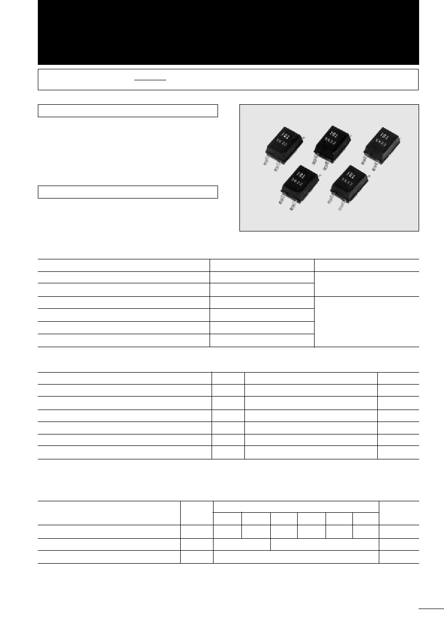
External View
Type No.
V
O
(V)
I
O
(A)
SAI01
5
SAI02
3.3
SAI03
12
SAI04
15
0.4
SAI05
13
SAI06
9
s
Absolute Maximum Ratings
Parameter
Symbol
Ratings
Unit
DC Input Voltage
V
IN
35
V
Power Dissipation
P
D
0.75
W
Junction Temperature
T
j
+125
∞
C
Storage Temperature
T
stg
≠40 to +125
∞
C
SW Terminal Applied Reverse Voltage
V
SW
≠1
V
Thermal Resistance* (junction-to-case)
R
th(j-c)
20
∞
C/W
* Refer to Outline Drawing for the case temperature measuring points.
s
Recommended Operating Conditions
0.5
s
Lineup
Switching Type
Surface-mount and Separate Excitation Type
Ratings
Parameter
Symbol
SAI01
SAI02
SAI03
SAI04
SAI05
SAI06
Unit
DC Input Voltage Range
V
IN
7 to 33 5.3 to 33 15 to 33 18 to 33 16 to 33 12 to 33
V
Output Current Range
I
O
0 to 0.5
0 to 0.4
A
Operating Junction Temperature Range
T
jop
≠30 to +125
∞
C

6
Ratings
Parameter
Symbol
SAI01
SAI02
SAI03
SAI04
SAI05
SAI06
Unit
min
typ max min
typ max min
typ max min
typ max min
typ max min
typ max
V
O
4.80
5.00 5.20
3.17 3.30 3.43 11.40 12.00 12.60 14.25 15.00 15.75 12.35 13.00 13.65 8.55 9.00 9.45
Condition
V
IN
=20V, I
O
=0.3A V
IN
=15V, I
O
=0.3A V
IN
=24V, I
O
=0.3A V
IN
=27V, I
O
=0.3A V
IN
=25V, I
O
=0.3A V
IN
=21V, I
O
=0.3A
80
75
88
89
88
86
Condition
VIN=20V, IO=0.3A
V
IN
=15V, I
O
=0.3A
V
IN
=24V, I
O
=0.3A
V
IN
=27V, I
O
=0.3A
V
IN
=25V, I
O
=0.3A
V
IN
=21V, I
O
=0.3A
f
60
60
60
60
60
60
Condition
V
IN
=20V, I
O
=0.3A
V
IN
=15V, I
O
=0.3A
V
IN
=24V, I
O
=0.3A
V
IN
=27V, I
O
=0.3A
V
IN
=25V, I
O
=0.3A
V
IN
=21V, I
O
=0.3A
V
OLINE
80
100
60
80
100
130
100
130
100
130
90
110
Condition V
IN
=10 to 30V, I
O
=0.3A V
IN
=8 to 30V, I
O
=0.3A V
IN
=18 to 30V, I
O
=0.3A V
IN
=21 to 30V, I
O
=0.3A V
IN
=19 to 30V, I
O
=0.3A V
IN
=15 to 30V, I
O
=0.3A
V
OLOAD
30
40
20
30
70
95
90
120
75
100
50
80
Condition V
IN
=20V, I
O
=0.1 to 0.4A V
IN
=15V, I
O
=0.1 to 0.4A V
IN
=24V, I
O
=0.1 to 0.4A V
IN
=27V, I
O
=0.1 to 0.4A V
IN
=25V, I
O
=0.1 to 0.4A V
IN
=21V, I
O
=0.1 to 0.4A
Temperature Coefficient
Vo/
T
±
0.5
±
0.5
±
1.5
±
1.5
±
1.5
±
1.0
of Output Voltage
R
REJ
45
45
45
45
45
45
Condition
f=100 to 120Hz
I
S
0.55
0.55
0.45
0.45
0.45
0.45
Condition
V
IN
=10V
V
IN
=8V
V
IN
=18V
V
IN
=21V
V
IN
=19V
V
IN
=15V
s
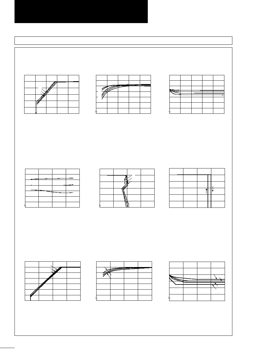
Electrical Characteristics
s
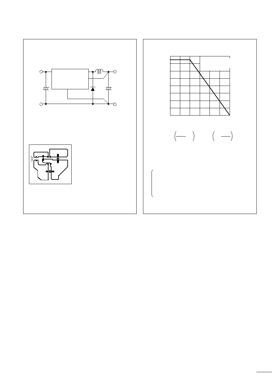
Outline Drawing (unit:mm)
s
Block Diagram
a. Type
b. Lot number
A Case temperature
measuring point
Plastic Mold Package Type
Flammability: UL94V-0
Weight: Approx. 0.22 g
SAI
Series
Output Voltage
V
Efficiency
%
Switching Frequency
kHz
Line Regulation
mV
Load Regulation
mV
mV/
∞
C
Ripple Rejection
dB
Overcurrent Protection
A
Starting Current
Terminal Connections
(1) Input
(2) Switching output
(3) Output Voltage
Detection
(4) Ground
A
3V
OS
a
b
4
.GND
2 SW
1V
IN
6.8
max.
4.0
max.
4.7
max.
2.54
±
0.25
4.32
±
0.2
8.0
±
0.5
3.6
±
0.2
1.4
±
0.2
3.0
±
0.2
9.8
±
0.3
0~0.1
6.3
±
0.2
1.0
±
0.3
0.89
±
0.15
0.26
0.75
+0.15
≠0.05
0.3
+0.15
≠0.05
SW
V
OS
V
IN
4
GND
3
2
1
Osc
Reg.
Ocp
Comp.
Reset
Drive
TSD
Amp.
V
REF
7
s
Example of Printed-circuit board
The efficiency depends on the input voltage and the
output current. Thus, obtain the value from the
efficiency graph on page 8 and substitute the per-
centage in the formula above.
V
O
: Output voltage
I
O
: Output current
: Efficiency (%)
V
F
: Diode forward voltage
SFPB54-0.3V
Thermal design for D
1
must be performed sepa-
rately.
s
Selecting external components
1. Inductor L1
q
It must be suited for switching regulators.
Do not use inductors for noise filters as they generate excessive heat.
w
It must have the appropriate inductance value.
If the inductance is too small (150
µ
H or lower), abnormal oscillation may occur causing operation problems in
the overcurrent protection circuit within the rated current range.
e
The rated current must be satisfied.
If the rated current is exceeded, magnetic saturation leads to overcurrent.
2. Capacitors C1 and C2
q
They must satisfy the breakdown voltage and allowable ripple current.
Use of these capacitors over their derating values shortens their service lives and may also cause abnormal
oscillation of the IC.
w
C
2
must be a low-impedance type capacitor.
A low-impedance type capacitor is recommended for C
2
to ensure minimum ripple voltage and stable switching
operation.
3. Diode D1
The Sanken SFPB54 diode is recommended for D
1
. If you intend to use an equivalent diode, be sure to make use
of a Schottky barrier diode and make sure that the reverse voltage applied to terminal 2 of the IC does not exceed
the value (≠1V) given in the absolute maximum ratings. If you use a fast recovery diode or any other diode, application
of a reverse voltage generated from the recovery or ON voltage of the diode may damage the IC.
a) For optimum operation,
there must be only one
GND line originating from
terminal 4 and each com-
ponent must be con-
nected with the shortest
possible wiring.
b) To prevent heating of the
IC, it is best to make the
GND pattern larger since
the internal frame and ter-
minal 4 (GND) are con-
nected to each other.
s
Standard External Circuit
s
Ta-PD Characteristics
+
+
V
IN
D
I1
C1
L
1
C
2
GND
SW
V
o
1
2
3
4
SAI
V
IN
C1
D1
L1
3.3
V
5
V
: 200
µ
H
12
V
13
V
15
V
: 300
µ
H
100
µ
F
C2
330
µ
F
V
IN
DC Input
V
OUT
DC Output
SFPB54
(Sanken)
GND
GND
GND
SAI
SW
V
OS
1
2
3
4
+
+
0.8
0.7
0.6
0.5
0.4
0.3
0.2
0.1
0
-30
0
25
50
75
100
125
∑ Glass epoxy substrate
(95
◊
69
◊
1.2)
∑ Natural cooling
Power Dissipation P
D
(W)
Ambient temperature Ta (
∞
C)
≠V
F
∑ I
O
V
O
1≠
V
IN
P
D
= V
O
∑ I
O
100
≠1