 | –≠–ª–µ–∫—Ç—Ä–æ–Ω–Ω—ã–π –∫–æ–º–ø–æ–Ω–µ–Ω—Ç: SAP10 | –°–∫–∞—á–∞—Ç—å:  PDF PDF  ZIP ZIP |
SAP
series
Part Number
SAP15P/SAP15N
SAP10P/SAP10N
SAP08P/SAP08N
150
100
80
160
150
150
15
12
10
0.22
0.22
0.22
5000 to 20000
5000 to 20000
5000 to 20000
P
C
(W)
V
CEO
( V )
I
C
(A)
Emitter resistor (
)
h
FE
R :70
Typ.
D
S
R
E
: 0.22
Typ.
E
C
B
B
D
R: 70
Typ.
C
S
E
Emitter resistor
R
E
: 0.22
Typ.
Emitter resistor
B D
S
C
E
E S
D
C
B
NPN
PNP
15.4
±
0.3
4.5
±
0.2
(7.62)
(12.7)
17.8
±
0.3
4
±
0.1
3.3
±
0.2
3.4max
5
±
0.2
22
±
0.3
23
±
0.3
28
±
0.3
2
±
0.1
(18)
(2.5)
(41)
7
±
0.2
9.9
±
0.2
1.6
±
0.2
3.2
±
0.2
1.35
(36
∞
)
+0.2
≠0.1
0.65
+0.2
≠0.1
0.8
+0.2
≠0.1
0.65
+0.2
≠0.1
1
±
0.1
2.54
±
0.1
2.54
±
0.1
3.81
±
0.1
3.81
±
0.1
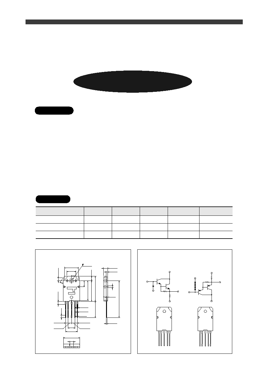
Darlington transistors with
built-in temperature compensation diodes
for audio amplifier applications
qBuilt-in temperature compensation diodes and one emitter resistor
qReal time temperature compensation
The temperature compensation diodes are mounted on one chip and placed in the center of the chip to
detect temperature rises directly.
qElimination of the temperature dependency of the idling current
The temperature coefficient of the diodes is optimized to have the idling current stabilized; thus one of
the fatal failure modes in conventional Darlington transistors, Thermal Runaway, is avoidable.
qSymmetrical design for the PNP and the NPN pinouts
The new design minimizes the length of the pattern layout, and output distortions are controlled.
qDarlington transistors, temperature compensation diodes and one emitter resistor are
incorporated in one package, so labor for parts insertion as well as the parts count is
reduced.
Features
Line up
sExternal Dimentions
(Unit : mm)
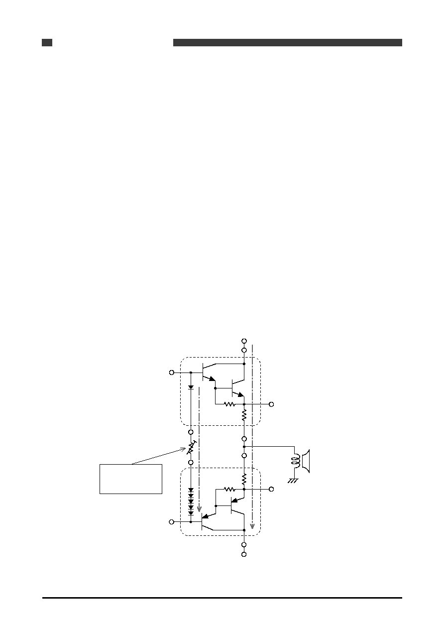
sEquivalent Circuit Diagram
a
b
Weight: approx 8.3g
a. Part Number
b. Lot Number
B
D
2.5mA
40mA
D
C
NPN
S
S
E
E
PNP
C
B
≠V
CC
+V
CC
Application Information
1. Recommended Operating Conditions
Add a variable resistor (VR) between diode terminals to adjust the idling current. The
resistor having 0 to 200
is to be used.
Adjust the forward current flowing over the diodes at 2.5mA.
Adjust the idling current at 40mA with the external variable resistor.
Both the temperature coefficients for the transistor and the diodes are matched under the above conditions.
Both the PNP and the NPN are Darlington transistors, so the temperature change ratio of the total four V
BE
of the transistors is subject to the compensation. One PN junction diode in the NPN and five Schottky
barrier diodes in the PNP are built-in, and the total six diodes are operating as the temperature compensation.
The temperature coefficient of the total diodes (its variable value) becomes smaller with a larger forward
current (approximately ≠ 0.2mV/
∞
C to 1mA), and the coefficient of the total transistors (its variable value)
also becomes smaller with a larger idling current (approximately ≠ 0.1mV/
∞
C to 10mA), but the both variable
values are small.
Thus, the distortion of the temperature coefficient caused by the different current is small, so the thermal
runaway may not be occurred due to the changes of the recommended ratings; however, the actual operation
is to be confirmed by using an experimental equipment or board.
External variable
resistor (VR)
(0 to 200
)

Di V
F
TR V
BE
Variations
Variations
V
BE
V
BE
Min.
(P and N: h
FE
Max.)
V
BE
Max.
(P and N: h
FE
Min.)
I
C
40mA
V
F
=500mV
2. External Variable Resistor
Total forward voltage (at I
F
=2.5mA) of the diodes is designed to be equal or less than that of total V
BE
(at I
C
= 40mA) of the transistor, thus the idling current is required to be adjusted at 40mA with an additional
external variable resistor.
The relations are shown as below:
Total V
F
of Diode Total V
BE
of Transistor + Total V
RE
of Emitter Resistor
V=0 to 500mV
The V
BE
of the transistor is dependent to the h
FE
, and the V
BE
is lower with higher h
FE
and vice versa. The
h
FE
for both the PNP and the NPN varies between 5k and 20k; thus the V
BE
is the lowest with the
combination of maximum h
FE
(20k) each and it is the highest with the combination of minimum h
FE
(5k)
each.
Presuming the voltage difference between the V
F
of the diodes and the V
BE
of the transistors (including the
total voltage drops of the two emitter resistors) as
V.
Minimum V
BE
≠ Maximum V
F
variations of the diodes = 0
Maximum V
BE
≠ Minimum V
F
variations of the diodes = 500mV
The current flowing over the diodes and the VR is adjusted at 2.5mA; therefore
500mV 2.5mA = 200
Consequently, the applicable VR value is to be 0 to 200
1.0
10.0
5.0
0
500
1000
1500
V
F
(mV)
I
F
(mA)
I
F ≠
V
F
Characteristics
2000
2500
3000
PN-Di
SBD
(5 diodes Total)
PN≠Di+SBD
3. Characteristics of the temperature compensation diodes
The several temperature compensation diodes are connected in series, so the forward voltage is varied with
small current fluctuations. Therefore, in case the forward current flowing over the diodes is set at 2.5mA and
over, the forward voltage rises, and in the worst combinations, the idling current reaches to 40mA and over
with minimum VR of 0
. On the contrary, in case the forward current is set at 2.5mA or below, the idling
current may not reach to 40mA with maximum VR of 200
.
4. Parallel push-pull application
Adjustments of the idling current are required by each the resistor in parallel push-pull applications. One
side adjustment will cause the idling current to be unstable (seesaw operation) because of the different h
FE
.
Ta=25
∞
C
To be adjusted individually
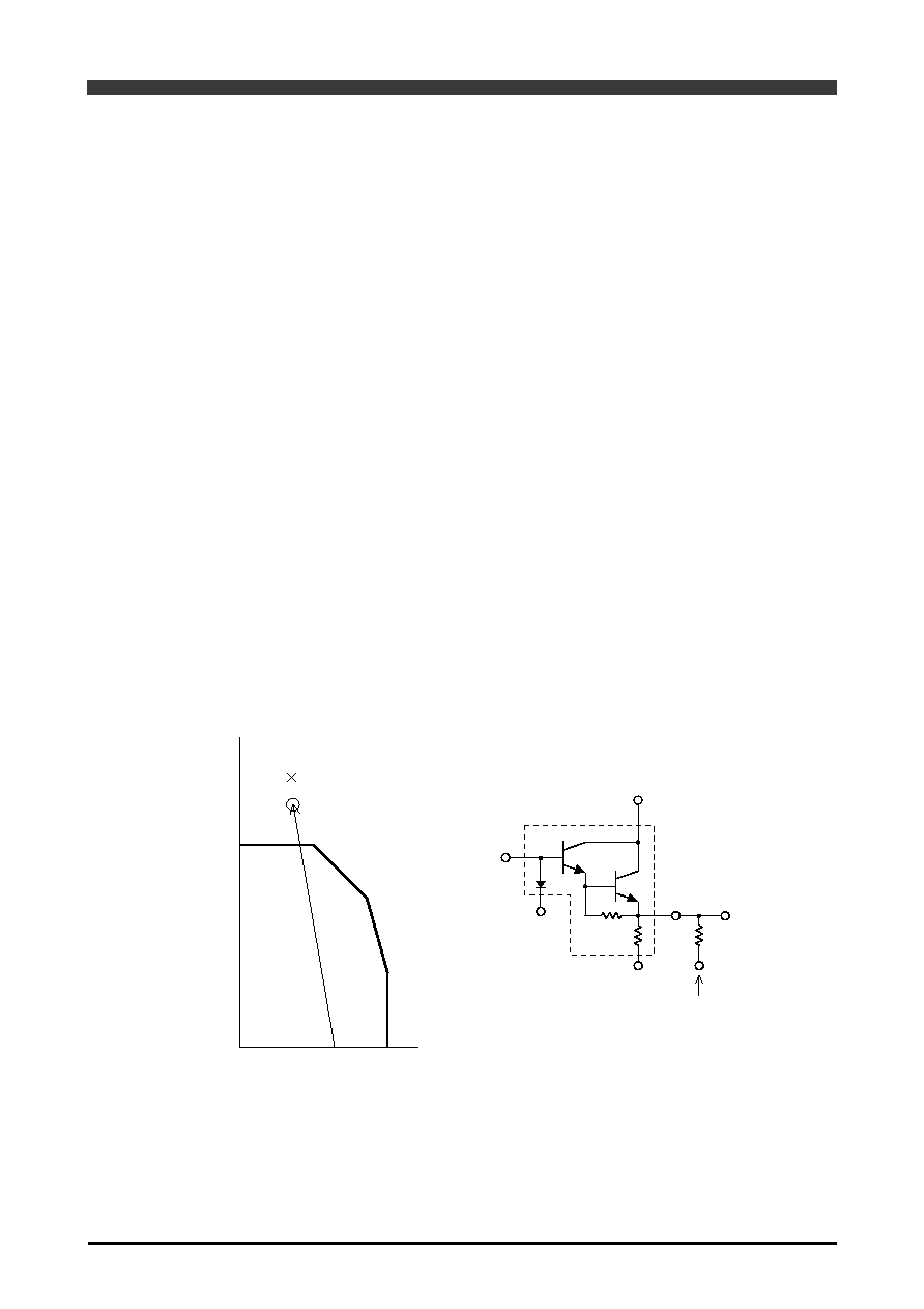
I
C
V
CE
Transistor destruction point
Thick-film resistor
destruction point
A.S.O.
Curve
B
D
C
S
E
5. Destruction capacity of the built-in emitter resistor
The built-in resistor is fabricated with polysilicone on the chip for the SAP08P/N and a thick-film resistor is
used for the SAP10P/N and SAP15P/N. The latter, the thick-film resistor, has weaker destruction point in
the Pc area (especially for large current flowing area) rather than that of the transistor chip itself. This is
subject to the area beyond Safe Operating Area (S.O.A).
However, under the evaluation like a short circuit test in which the current exceeds the guaranteed value, it
may cause the emitter resistor to be destroyed before the transistor itself is destroyed.
Consequently, the current value (or time) that operates the protection circuit is to be set at lower than that of
discrete device configurations. In the application of car audio amplifiers, the same manners as the above
need to be considered because the large current is flowed at low impedance.
In addition, once the transistor falls into thermal runaway due to a soldering failure to the external VR added
between diodes or other failure manners, as the worst case, there may cause a resin crack or smoke emissions
by flare up. Flame retardant molding resin is used, and the material of the product is conformed to the most
sever standard UL94V0. However it is recommended that the careful consideration be given to a protection
circuit, and the protection circuits should be provided appropriately in due course.
If the operating conditions are not to be matched to the ratings, it is also recommended that the E (Emitter
resistor) terminal should be opened and the external emitter resistor should be added to the S (Sensing)
terminal shown as below. (However this is not applicable to the SAP08P/N because a thin inner lead is used
for S terminal.)
External
emitter resistor
Output terminal