 | –≠–ª–µ–∫—Ç—Ä–æ–Ω–Ω—ã–π –∫–æ–º–ø–æ–Ω–µ–Ω—Ç: SI-3123N | –°–∫–∞—á–∞—Ç—å:  PDF PDF  ZIP ZIP |

12
Parameter
DC Input Voltage
DC Output Current
Power Dissipation
Junction Temperature
Ambient Operating Temperature
Storage Temperature
Thermal Resistance (junction to case)
Thermal Resistance (junction to ambient air)
I
Features
∑ Compact full-mold package (equivalent to TO220)
∑ Output current: 1.0A
∑ Low dropout voltage: V
DIF
0.5V (at I
O
=1.0A)
∑ Built-in dropping overcurrent, overvoltage, thermal protection circuits
∑ Supports constant current load and plus/minus power supplies.
I
Applications
∑ For stabilization of the secondary stage of switching power supplies
∑ Electronic equipment
I
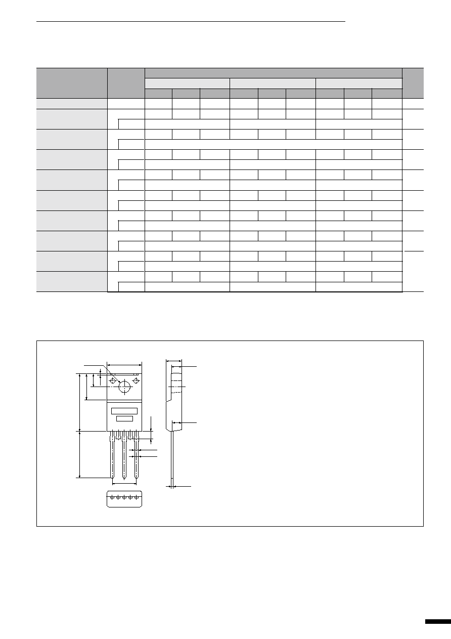
Absolute Maximum Ratings
(T
a
=25
∞
C)
SI-3003N Series
3-Terminal, Full-Mold, Low Dropout Voltage Dropper Type
G
SI-3003N Series
Ratings
SI-3053N
SI-3123N
SI-3153N
25
30
30
1.0*
1
20(With infinite heatsink)
1.5(Without heatsink, stand-alone operation)
≠40 to +125
≠30 to +100
≠40 to +125
5.0
66.7(Without heatsink, stand-alone operation)
Symbol
V
IN
I
O
P
D1
P
D2
T
j
T
op
T
stg
R
th(j-c)
R
th(j-a)
Unit
V
A
W
W
∞
C
∞
C
∞
C
∞
C/W
∞
C/W
13
I
Electrical Characteristics
Unit
V
V
V
mV
mV
mV/
∞
C
dB
mA
A
I
External Dimensions
a. Part Number
b. Lot Number
Pin Arrangement
q
GND
w
V
O
e
V
IN
Plastic Mold Package Type
Flammability: UL94V-0
Weight: Approx. 2.3g
0.95
±
0.15
0.85
+0.2
10
±
0.2
4.2
±
0.2
2.8
±
0.2
2.6
±
0.15
q
w
e
3.2
±
0.2
2
max.
0.5
16.9
±
0.3
7.9
±
0.2
4
±
0.2
(13.5)
0.45
+0.2
≠0.1
P3.4
±
0.1
◊
2=6.8
≠0.1
a
b
G
SI-3003N Series
Symbol
V
IN
V
O
Conditions
V
DIF
Conditions
V
OLINE
Conditions
V
OLOAD
Conditions
V
O
/
T
a
Conditions
R
REJ
Conditions
I
q
Conditions
I
S1
Conditions
I
S2
Conditions
(unit:mm)
(T
a
=25
∞
C unless otherwise specified)
Parameter
Input Voltage
Output Voltage
Dropout Voltage
Line Regulation
Load Regulation
Temperature Coefficient
of Output Voltage
Ripple Rejection
Quiescent Circuit
Current
Overcurrent Protection
Starting Current
*4,5
Limited Current at
Overcurrent Protection
*1: V
IN(max)
and I
O(max)
are restricted by the relation P
D(max)
=(V
IN
-V
O
)∑I
O
=20(W).
*2: Refer to the dropout voltage.(Refer to Setting DC Input Voltage on page 7.)
*3: I
S
1 is specified at ≠5(%) drop point of output voltage V
O
on the condition that V
IN
=V
O
+3V, I
O
=1A.
Ratings
SI-3053N
SI-3123N
SI-3153N
min.
typ.
max.
min.
typ.
max.
min.
typ.
max.
6
*2
15
*1
13
*2
22
*1
16
*2
25
*1
4.90
5.00
5.10
11.76
12.00
12.24
14.70
15.00
15.30
V
IN
=8V, I
O
=1.0A
V
IN
=15V, I
O
=1.0A
V
IN
=18V, I
O
=1.0A
0.5
0.5
0.5
I
O
1.0A
10
30
24
64
30
90
V
IN
=6V to 15V, I
O
=1.0A
V
IN
=13V to 22V, I
O
=1.0A
V
IN
=16V to 25V, I
O
=1.0A
20
50
40
120
50
150
V
IN
=8V, I
O
=0 to 1.0A
V
IN
=15V, I
O
=0 to 1.0A
V
IN
=18V, I
O
=0 to 1.0A
±
0.5
±
1.5
±
1.5
V
IN
=8V, I
O
=5mA, T
j
=0 to 100
∞
C
V
IN
=15V, I
O
=5mA, T
j
=0 to 100
∞
C V
IN
=18V, I
O
=5mA, T
j
=0 to 100
∞
C
54
54
54
V
IN
=8V, f=100 to 120H
Z
V
IN
=15V, f=100 to 120H
Z
V
IN
=18V, f=100 to 120H
Z
3
10
3
10
3
10
V
IN
=8V, I
O
=0A
V
IN
=15V, I
O
=0A
V
IN
=18V, I
O
=0A
1.2
1.2
1.2
V
IN
=8V
V
IN
=15V
V
IN
=18V
1.2
1.2
1.2
V
IN
=8V, V
O
=0A
V
IN
=15V, V
O
=0A
V
IN
=18V, V
O
=0A
14
I
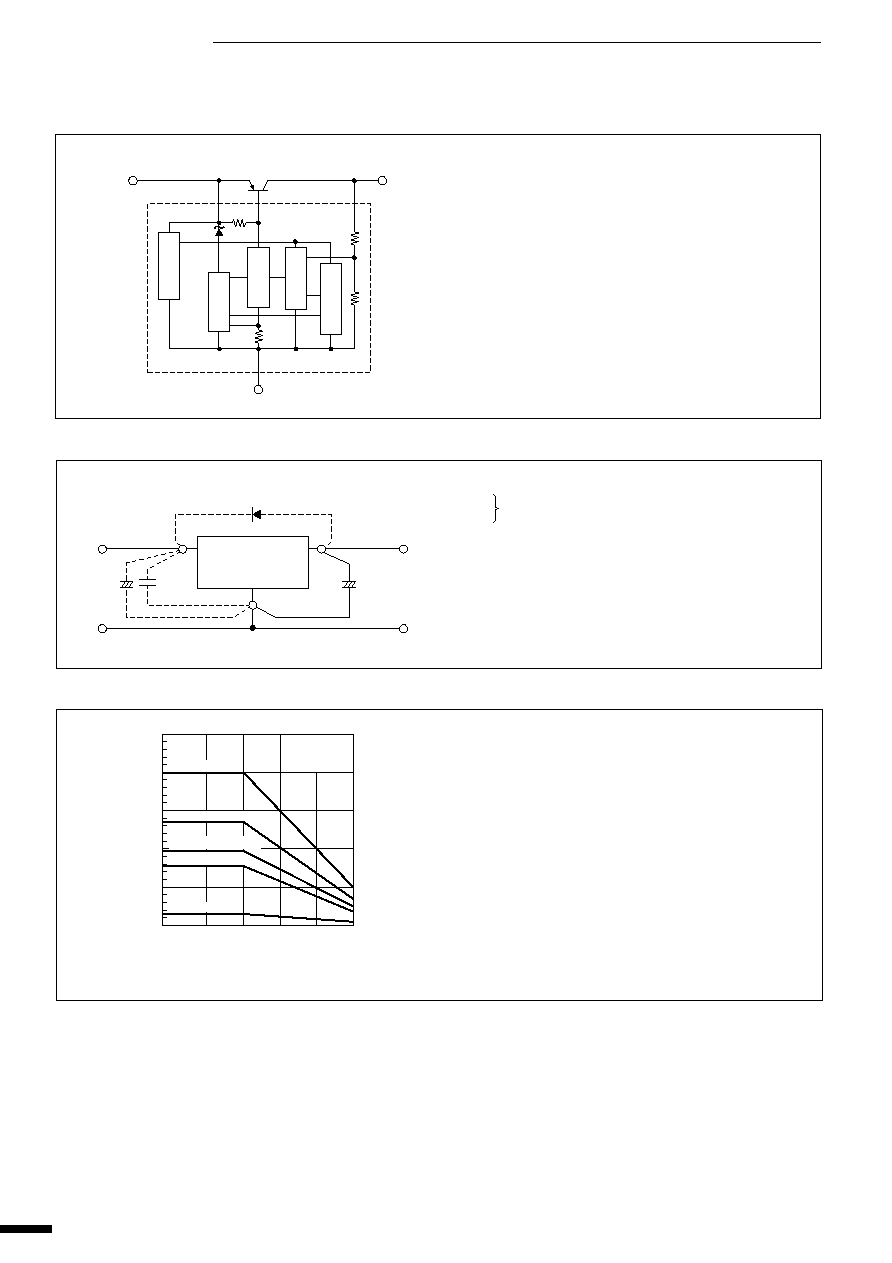
Block Diagram
I
Standard External Circuit
3
Reg.
Protection
Amp.
V
REF
Drive
MIC
1
2
T
r1
D
1
C
0
C
2
C
1
DC Input
DC Output
V
IN
V
O
GND
GND
3
2
1
SI-3003N
*
1
*
2
+
+
I
T
a
-P
D
Characteristics
P
D
=I
O
∑[V
IN
(mean)≠V
O
]
C
0
: Output capacitor (47 to 100
µ
F)
*1 C
1
: Oscillation prevention capacitor
C
2
(C
1
: Approx. 47
µ
F, C
2
: 0.33
µ
F)
These capacitors are required if the input line is inductive
and in the case of long wiring. Tantalum capacitors are
recommended for C
1
and C
0
, particularly at low tempera-
tures.
*2 D
1
: Protection diode
This diode is required for protection against reverse bias-
ing of the input and output. Sanken EU2Z is recommended.
25
20
15
10
5
0
Power Dissipation P
D
(W)
75
◊
75
◊
2mm (7.6
∞
C/W)
100
◊
100
◊
2mm (5.2
∞
C/W)
200
◊
200
◊
2mm (2.3
∞
C/W)
≠30
0
25
50
Ambient Temperature T
a
(
∞
C)
75
100
Infinite heatsink
Without heatsink
With Silicon Grease
Heatsink: Aluminum
G
SI-3003N Series
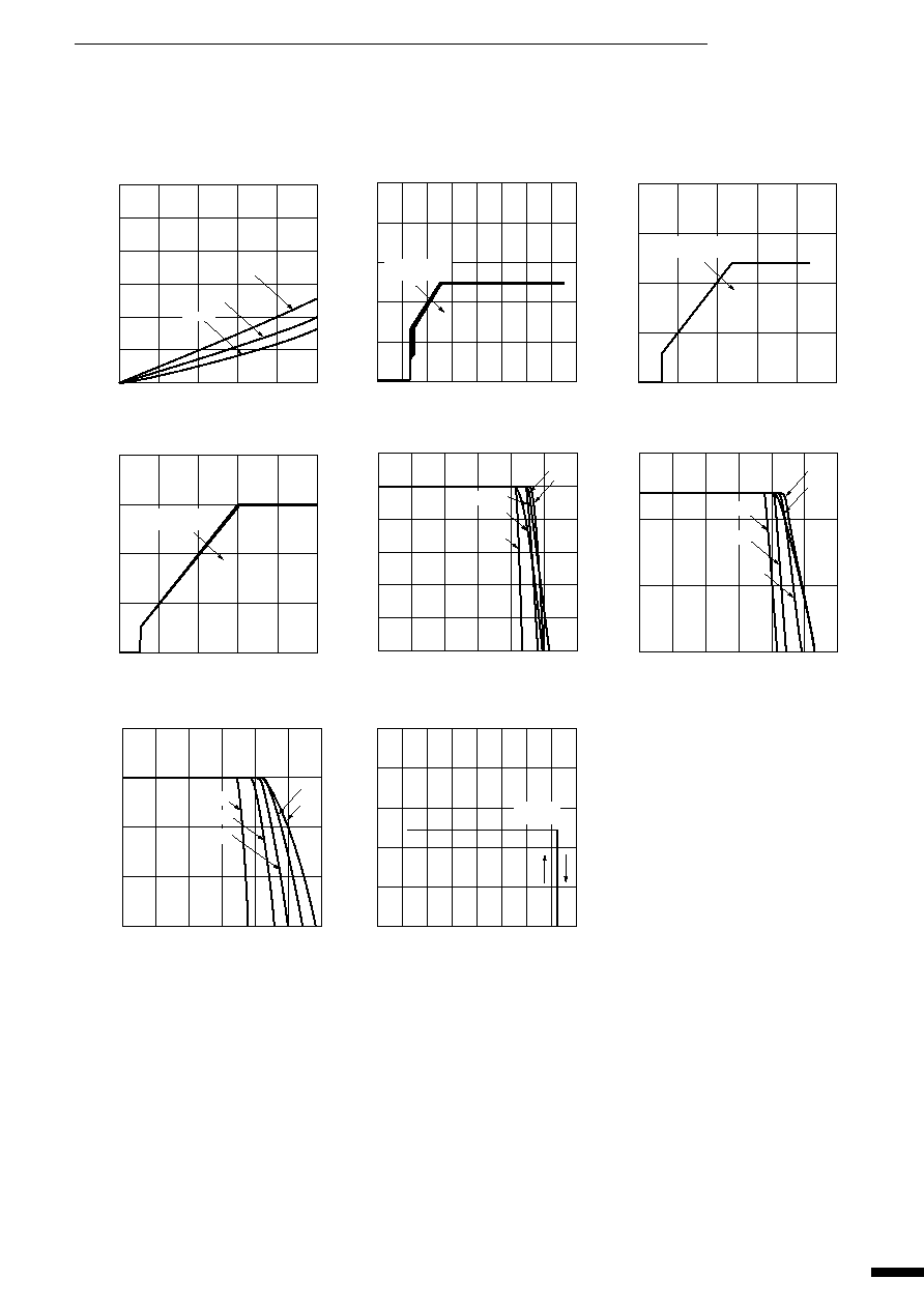
15
I
Typical Characteristics
I
O
vs. V
DIF
Characteristics
Output Voltage(SI-3053N)
Output Voltage(SI-3123N)
Output Voltage(SI-3153N)
Overcurrent Protection Characteristics(SI-3053N)
Overcurrent Protection Characteristics(SI-3123N)
Overcurrent Protection Characteristics(SI-3153N)
Thermal Protection Characteristics(SI-3053N)
Output Voltage V
O
(V)
0
2
4
6
8
Input Voltage V
IN
(V)
10
12
14
16
10
8
6
4
2
0
I
O
=
0 to 1A
(0.25A step)
Input Voltage V
IN
(V)
Output Voltage V
O
(V)
20
15
10
5
00
5
10
15
20
25
I
O
=
0 to 1A
(0.25A step)
Output Voltage V
O
(V)
Input Voltage V
IN
(V)
20
15
10
5
0
I
O
=
0 to 1A
(0.25A step)
0
5
10
15
20
25
Output Current I
O
(A)
6
5
4
3
2
1
0
0
0.5
1.0
1.5
2.0
2.5
3.0
V
IN
=12V
8V
10V
6V
15V
Output Voltage V
O
(V)
Output Current I
O
(A)
15
10
5
0
0
0.5
1.0
1.5
2.0
2.5
3.0
V
IN
=22V
15V
13V
18V
20V
Output Voltage V
O
(V)
Output Current I
O
(A)
20
15
10
5
0
0
0.5
1.0
1.5
2.0
2.5
3.0
V
IN
=25V
18V
16V
22V
Output Voltage V
O
(V)
20V
Ambient Temperature T
a
(
∞
C)
Output Voltage V
O
(V)
10
8
6
4
2
0
0
20
40
60
80
100
120
140
160
V
IN
=8V
I
O
=10mA
Note on Thermal Protection:
The thermal protection circuit is intended for
protection against heat during instantaneous
short-circuiting. Its operation is not guaran-
teed for continuous heating condition such
as short-circuiting over extended periods of
time.
(T
a
=25
∞
C)
G
SI-3003N Series
Output Current I
O
(A)
Dropout Voltage V
DIF
(V)
0.6
0.5
0.4
0.3
0.2
0.1
0
0
0.2
0.4
0.6
0.8
1.0
≠30
∞
C
25
∞
C
100
∞
C