 | –≠–ª–µ–∫—Ç—Ä–æ–Ω–Ω—ã–π –∫–æ–º–ø–æ–Ω–µ–Ω—Ç: SI-3150 | –°–∫–∞—á–∞—Ç—å:  PDF PDF  ZIP ZIP |
39
Unit
V
V
A
W
W
∞
C
∞
C
∞
C
∞
C/W
∞
C/W
Symbol
V
IN
V
C
I
O
P
D1
P
D2
T
j
T
op
T
stg
R
th(j-c)
R
th(j-a)
s
Features
∑ Compact full-mold package (equivalent to TO220)
∑ Output current: 1.5A
∑ Low dropout voltage: V
DIF
1V (at I
O
=1.5A)
∑ Variable output voltage (rise only)
May be used for remote sensing
∑ Output ON/OFF control terminal is compatible with LS-TTL. (It may be
directly driven by LS-TTL or standard CMOS logic.)
∑ Built-in foldback overcurrent (SI-3033C: Drooping type overcurrent), ov-
ervoltage, thermal protection circuits
s
Applications
∑ For stabilization of the secondary stage of switching power supplies
∑ Electronic equipment
s
Absolute Maximum Ratings
(T
a
=25
∞
C)
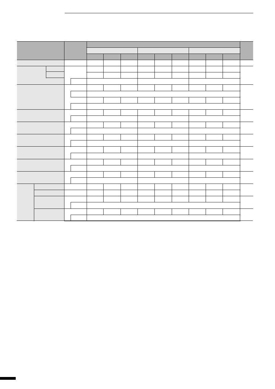
SI-3000C Series
5-Terminal, Multi-Function, Full-Mold, Low Dropout Voltage Dropper Type
Ratings
SI-3033C
SI-3050C/3090C SI-3120C/3150C
SI-3240C
20
35
35
45
V
IN
1.5
*2
18(With infinite heatsink)
1.5(Without heatsink, stand-alone operation)
≠40 to +125
≠30 to +100
≠40 to +125
5.5
66.7(Without heatsink, stand-alone operation)
q
SI-3000C Series
Parameter
DC Input Voltage
Voltage of Output Control Terminal
DC Output Current
Power Dissipation
Junction Temperature
Ambient Operating Temperature
Storage Temperature
Thermal Resistance (junction to case)
Thermal Resistance (junction to ambient air)
40
Parameter
Input Voltage
Output Voltage
Dropout Voltage
Line Regulation
Load Regulation
Temperature Coefficient
of Output Voltage
Ripple Rejection
Quiescent Circuit Current
Overcurrent Protection
Starting Current
*4,6
Control Voltage (Output ON)
Control Voltage (Output OFF)
Control Current
(Output ON)
Control Current
(Output OFF)
Symbol
V
IN
V
O
Conditions
V
DIF
Conditions
Conditions
V
OLINE
Conditions
V
OLOAD
Conditions
V
O
/
T
a
Conditions
R
REJ
Conditions
I
q
Conditions
I
S1
Conditions
V
C.
IH
V
C.
IL
I
C.
IH
Conditions
I
C.
IL
Conditions
s
Electrical Characteristics
*1: "A" may be indicated to the right of the Sanken logo.
*2: V
IN(max)
and I
O(max)
are restricted by the relation P
D(max)
=(V
IN
-V
O
)∑I
O
=18(W).
*3: Refer to the dropout voltage.(Refer to Setting DC Input Voltage on page 7.)
*4: I
S
1 is specified at ≠5(%) drop point of output voltage V
O
on the condition that V
IN
=V
O
+3V, I
O
=0.5A.
*5: Output is ON even when output control terminal V
C
is open. Each input level is equivalent to LS-TTL. Therefore, it may be directly driven by an
LS-TTL circuit.
*6: A foldback type overcurrent protection circuit is built into the I
C
regulator (excluding SI-3033C). Therefore, avoid using it for the following applica-
tions as it may cause starting errors:
(1) Constant current load (2) Plus/minus power (3) Series power (4) V
O
adjustment by raising ground voltage
Unit
V
V
V
mV
mV
mV/
∞
C
dB
mA
A
V
µ
A
mA
SI-3000C
*1
SI-3000CA
Ratings
SI-3033C
SI-3050C
SI-3090C
min.
typ.
max.
min.
typ.
max.
min.
typ.
max.
*3
15
*2
6
*3
30
*2
10
*3
30
*2
3.168
3.300
3.432
4.80
5.00
5.20
8.64
9.00
9.36
3.234
3.300
3.366
4.90
5.00
5.10
8.82
9.00
9.18
V
IN
=5V, I
O
=1.0A
V
IN
=8V, I
O
=1.0A
V
IN
=12V, I
O
=1.0A
0.5
0.5
0.5
I
O
1.0A
1.0
1.0
1.0
I
O
1.5A
10
30
10
30
18
48
V
IN
=4.5 to 12V, I
O
=1.0A
V
IN
=6 to 15V, I
O
=1.0A
V
IN
=10 to 20V, I
O
=1.0A
40
100
40
100
70
180
V
IN
=5V, I
O
=0 to 1.5A
V
IN
=8V, I
O
=0 to 1.5A
V
IN
=12V, I
O
=0 to 1.5A
±
0.5
±
0.5
±
1.0
V
IN
=5V, I
O
=5mA, T
j
=0 to 100
∞
C V
IN
=8V, I
O
=5mA, T
j
=0 to 100
∞
C V
IN
=12V, I
O
=5mA, T
j
=0 to 100
∞
C
54
54
54
V
IN
=5V, f=100 to 120H
Z
V
IN
=8V, f=100 to 120H
Z
V
IN
=12V, f=100 to 120H
Z
3
10
5
10
5
10
V
IN
=5V, I
O
=0A
V
IN
=8V, I
O
=0A
V
IN
=12V, I
O
=0A
1.6
1.6
1.6
V
IN
=5V
V
IN
=8V
V
IN
=12V
2.0
2.0
2.0
0.8
0.8
0.8
20
20
20
V
C
=2.7V
≠0.3
≠0.3
≠0.3
V
C
=0.4V
(T
a
=25
∞
C unless otherwise specified)
q
SI-3000C Series
V
C
Terminal
*5
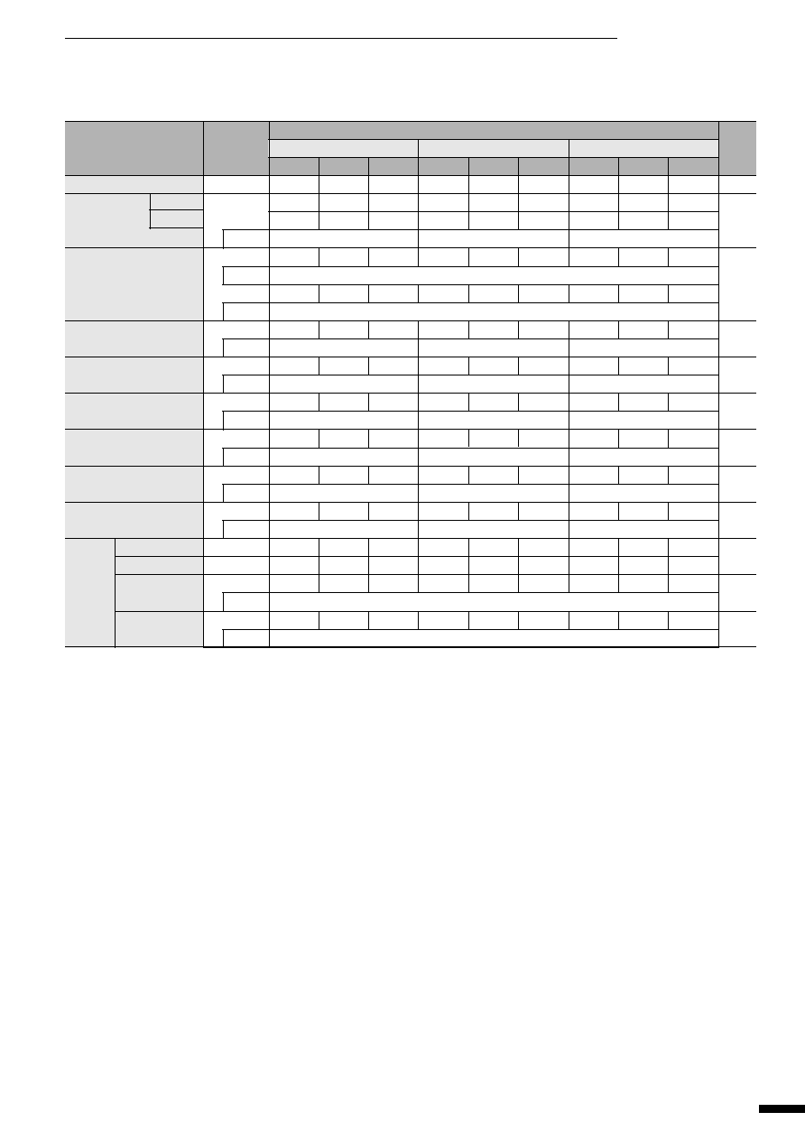
41
Parameter
Input Voltage
Output Voltage
Dropout Voltage
Line Regulation
Load Regulation
Temperature Coefficient
of Output Voltage
Ripple Rejection
Quiescent Circuit Current
Overcurrent Protection
Starting Current
*4,6
Control Voltage (Output ON)
Control Voltage (Output OFF)
Control Current
(Output ON)
Control Current
(Output OFF)
s
Electrical Characteristics
*1: "A" may be indicated to the right of the Sanken logo.
*2: V
IN(max)
and I
O(max)
are restricted by the relation P
D(max)
=(V
IN
-V
O
)∑I
O
=18(W).
*3: Refer to the dropout voltage.(Refer to Setting DC Input Voltage on page 7.)
*4: I
S
1 is specified at ≠5(%) drop point of output voltage V
O
on the condition that V
IN
=V
O
+3V, I
O
=0.5A.
*5: Output is ON even when output control terminal V
C
is open. Each input level is equivalent to LS-TTL. Therefore, it may be directly driven by an
LS-TTL circuit.
*6: A foldback type overcurrent protection circuit is built into the I
C
regulator (excluding SI-3033C). Therefore, avoid using it for the following applica-
tions as it may cause starting errors:
(1) Constant current load (2) Plus/minus power (3) Series power (4) V
O
adjustment by raising ground voltage
Unit
V
V
V
mV
mV
mV/
∞
C
dB
mA
A
V
µ
A
mA
Symbol
V
IN
V
O
Conditions
V
DIF
Conditions
Conditions
V
OLINE
Conditions
V
OLOAD
Conditions
V
O
/
T
a
Conditions
R
REJ
Conditions
I
q
Conditions
I
S1
Conditions
V
C.
IH
V
C.
IL
I
C.
IH
Conditions
I
C.
IL
Conditions
Ratings
SI-3120C
SI-3150C
SI-3240C
min.
typ.
max.
min.
typ.
max.
min.
typ.
max.
13
*3
30
*2
16
*3
30
*2
25
*3
40
*2
11.52
12.00
12.48
14.40
15.00
15.60
23.04
24.00
24.96
11.76
12.00
12.24
14.70
15.00
15.30
23.52
24.00
24.48
V
IN
=15V, I
O
=1.0A
V
IN
=18V, I
O
=1.0A
V
IN
=27V, I
O
=1.0A
0.5
0.5
0.5
I
O
1.0A
1.0
1.0
1.0
I
O
1.5A
24
64
30
90
48
128
V
IN
=13 to 25V, I
O
=1.0A
V
IN
=16 to 25V, I
O
=1.0A
V
IN
=25 to 38V, I
O
=1.0A
93
240
120
300
120
300
V
IN
=15V, I
O
=0 to 1.5A
V
IN
=18V, I
O
=0 to 1.5A
V
IN
=27V, I
O
=0 to 1.5A
±
1.5
±
1.5
±
2.5
V
IN
=15V, I
O
=5mA, T
j
=0 to 100
∞
C
V
IN
=18V, I
O
=5mA, T
j
=0 to 100
∞
C
V
IN
=27V, I
O
=5mA, T
j
=0 to 100
∞
C
54
54
54
V
IN
=15V, f=100 to 120H
Z
V
IN
=18V, f=100 to 120H
Z
V
IN
=27V, f=100 to 120H
Z
5
10
5
10
5
10
V
IN
=15V, I
O
=0A
V
IN
=18V, I
O
=0A
V
IN
=27V, I
O
=0A
1.6
1.6
1.6
V
IN
=15V
V
IN
=18V
V
IN
=27V
2.0
2.0
2.0
0.8
0.8
0.8
20
20
20
V
C
=2.7V
≠0.3
≠0.3
≠0.3
V
C
=0.4V
q
SI-3000C Series
(T
a
=25
∞
C unless otherwise specified)
V
C
Terminal
*5
SI-3000C
*1
SI-3000CA

42
q
GND
w
V
C
e
V
O
r
V
OS
t
V
IN
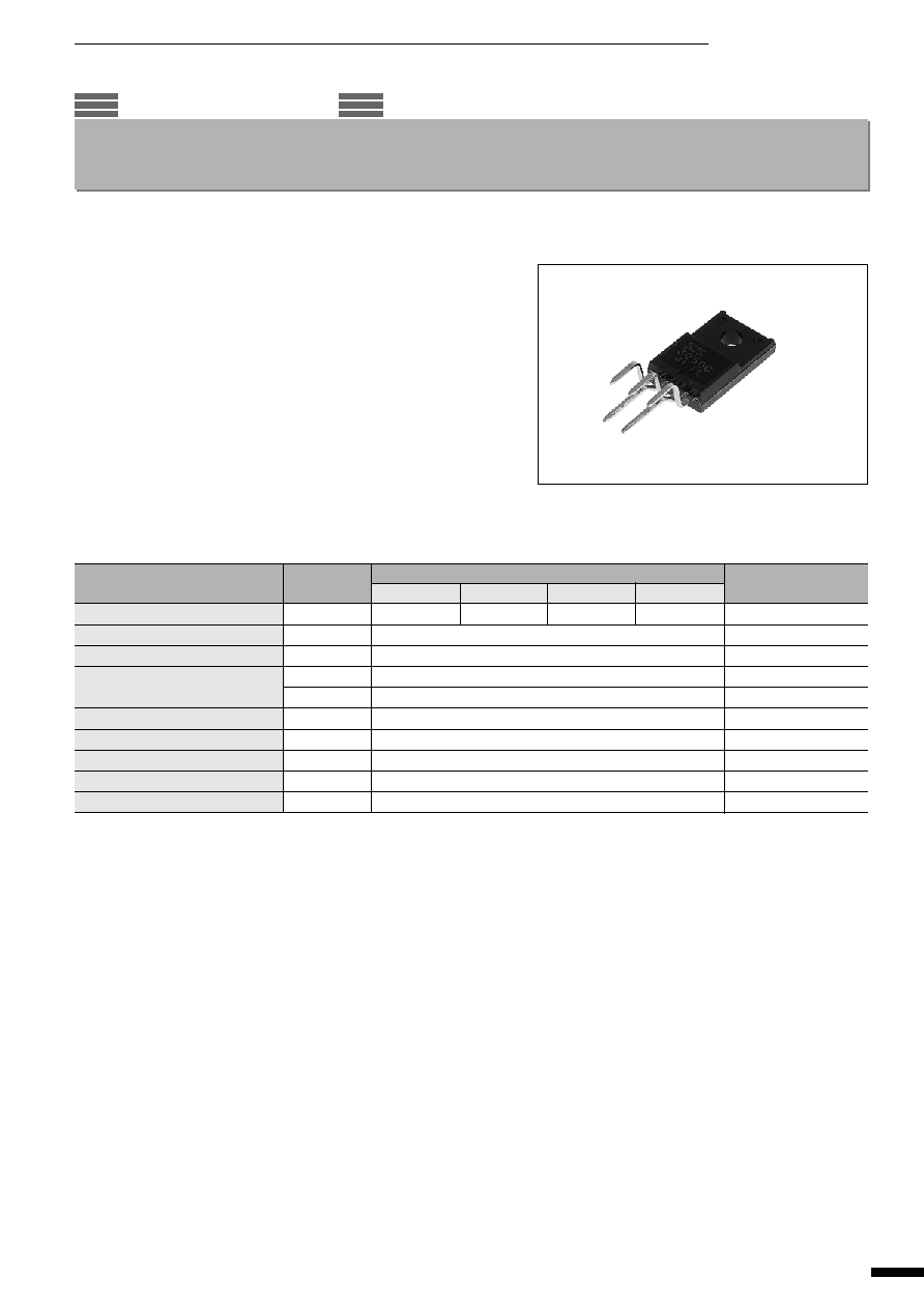
Plastic Mold Package Type
Flammability: UL94V-0
Weight: Approx. 2.3g
s
Block Diagram
SI-3000C
s
Standard External Circuit
C
0
: Output capacitor (47 to 100
µ
F)
*1 C
1
: Oscillation prevention capacitor (C
1
: Approx. 47
µ
F,
C
2
C
2
: 0.33
µ
F)
These capacitors are required if the input line is inductive
and in the case of long wiring. Tantalum capacitors are rec-
ommended for C
1
and C
0
, particularly at low temperatures.
*2 D
1
: Protection diode
This diode is required for protection against reverse biasing
of the input and output. Sanken EU2Z is recommended.
s
Outline Drawing
1
2
5
Reg.
ON/OFF
Protection
Drive
Amp.
V
REF
3
4
MIC
T
r1
Equivalent
to LS-TTL
D
1
C
0
C
2
C
1
DC Input
V
IN
DC Output
V
O
5
SI-3000C
OPEN
2
3
4
1
*
1
*
2
+
+
(unit:mm)
q
SI-3000C Series
10.0
±
0.2
4.2
±
0.2
0.95
±
0.15
8.2
±
0.7
2.6
±
0.1
3.9
±
0.7
(4.3)
(4.6)
(8.0)
(17.9)
(2.0)
0.85
+0.2
≠0.1
0.45
+0.2
≠0.1
3.2
±
0.2
4.0
±
0.2
7.9
±
0.2
5.0
±
0.6
16.9
±
0.3
0.5
1 2 3 4 5
P1.7
±
0.7
◊
4=6.8
±
0.7
2.8
±
0.2
Forming No. 1101
Part Number
Lot Number
43
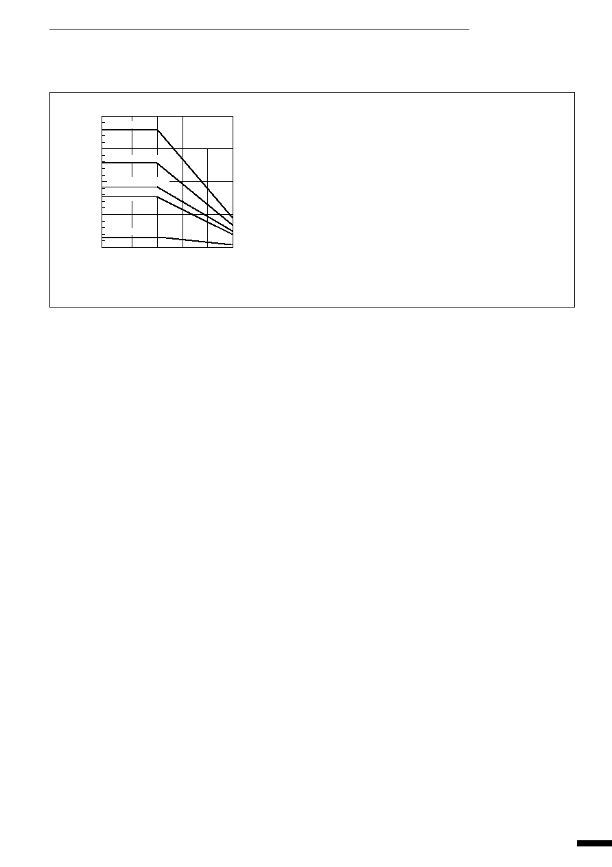
s
T
a
-P
D
Characteristics
P
D
=I
O
∑[V
IN
(mean)≠V
O
]
q
SI-3000C Series
15
20
10
5
0
≠30
0
25
50
Ambient Temperature T
a
(
∞
C)
Power Dissipation P
D
(W)
75
100
75
◊
75
◊
2mm (7.6
∞
C/W)
100
◊
100
◊
2mm (5.2
∞
C/W)
200
◊
200
◊
2mm (2.3
∞
C/W)
Infinite heatsink
Without heatsink
With Silicon Grease
Heatsink: Aluminum