86
s
Features
∑ High output current (6A:STR7000 series, 12A: STR7100 series)
∑ High efficiency (70 to 90%)
∑ Wide DC input voltage range
∑ Built-in drooping type overcurrent protection circuit
∑ Foldback type overcurrent protection can be set externally.
∑ Output voltage adjustment
∑ Built-in reference oscillator (35kHz)
∑ Output ON/OFF control
s
Applications
∑ Electronic equipment
s
Lineup
s
Absolute Maximum Ratings
Power Section: STR7000/STR7100 (T
a
=25
∞
C)
s
Control Section: SI-8020 Series (T
a
=25
∞
C)
Separate Excitation Switching Type
STR7000+SI-8020 Series
q
STR7000+SI-8020 Series
Unit
V
W
∞
C
∞
C
Symbol
V
IN
P
D
T
OP
T
Stg
V
O
(V)
I
O
(A)
6
12
Paraneter
DC Input Voltage
Power Dissipation
Operating Temperature
Storage Temperature
Unit
V
V
V
A
W
W
∞
C/W
∞
C
∞
C
∞
C
Symbol
V
4-1
V
4-5
V
1-2
I
C
P
D1
P
D2
R
th(j-c)
T
j
T
OP
T
Stg
Parameter
Power Transistor Breakdown Voltage
Drive Transistor Breakdown Voltage
Diode Breakdown Voltage
Collector Current
Power Dissipation
Power Transistor Thermal Resistance
Power Transistor Junction Temperature
Operating Temperature
Storage Temperature
Ratings
55
1
≠20 to +85
≠20 to +100
Ratings
STR7000 Series
STR7100 Series
60
60
60
6(peak 7.5)
12(peak 15)
100(T
C
=25
∞
C)
125(T
C
=25
∞
C)
4.3(Without heatsink)
1.25
1.0
+150
≠30 to +125(T
C
)
≠30 to +125
5
12
15
24
STR7001+SI-8020
STR7002+SI-8021
STR7002+SI-8022
STR7003+SI-8023
STR7101+SI-8020
STR7102+SI-8021
STR7102+SI-8022
STR7103+SI-8023
87
q
STR7000+SI-8020 Series
s
Electrical Characteristics: 6A Type
(T
a
=25
∞
C)
Unit
V
V
%
kH
Z
mV
mV
dB
A
A
s
Electrical Characteristics: 12A Type
(T
a
=25
∞
C)
Unit
V
V
%
kH
Z
mV
mV
dB
A
A
Symbol
V
IN
V
O
Conditions
Conditions
f
Conditions
V
OLINE
Conditions
V
OLOAD
Conditions
R
REJ
Conditions
I
S1
I
S2
Conditions
Parameter
DC Input Voltage Range
Output Voltage
Efficiency
Switching Frequency
Line Regulation
Load Regulation
Ripple Rejection
Overcurrent Protection Starting Current
Limited Current at Overcurrent
Protection Operation
Parameter
DC Input Voltage Range
Output Voltage
Efficiency
Switching Frequency
Line Regulation
Load Regulation
Ripple Rejection
Overcurrent Protection Starting Current
Limited Current at Overcurrent
Protection Operation
Ratings
STR7101+SI-8020
STR7102+SI-8021
STR7102+SI-8022
STR7103+SI-8023
min.
typ.
max.
min.
typ.
max.
min.
typ.
max.
min.
typ.
max.
11
40
18
50
21
50
30
50
5.0
5.1
5.2
11.8
12.0
12.2
14.8
15.0
15.2
23.7
24.0
24.3
V
IN
=20V, I
O
=6.0A
V
IN
=27V, I
O
=6.0A
V
IN
=30V, I
O
=6.0A
V
IN
=40V, I
O
=6.0A
70
82
84
87
V
IN
=20V, I
O
=6.0A
V
IN
=27V, I
O
=6.0A
V
IN
=30V, I
O
=6.0A
V
IN
=40V, I
O
=6.0A
35
35
35
35
V
IN
=20V, I
O
=6.0A
V
IN
=27V, I
O
=6.0A
V
IN
=30V, I
O
=6.0A
V
IN
=40V, I
O
=6.0A
80
120
150
200
V
IN
=15 to 25V, I
O
=6.0A
V
IN
=22 to 32V, I
O
=6.0A
V
IN
=25 to 35V, I
O
=6.0A
V
IN
=35 to 45V, I
O
=6.0A
30
40
40
50
V
IN
=20V, I
O
=3 to 9A
V
IN
=27V, I
O
=3 to 9A
V
IN
=30V, I
O
=3 to 9A
V
IN
=40V, I
O
=3 to 9A
45
45
45
45
f=100 to 120H
Z
f=100 to 120H
Z
f=100 to 120H
Z
f=100 to 120H
Z
12
15
12
15
12
15
12
15
12
15
12
15
12
15
12
15
R
S
=0.01
R
S
=0.01
R
S
=0.01
R
S
=0.01
Ratings
STR7001+SI-8020
STR7002+SI-8021
STR7002+SI-8022
STR7003+SI-8023
min.
typ.
max.
min.
typ.
max.
min.
typ.
max.
min.
typ.
max.
11
40
18
50
21
50
30
50
5.0
5.1
5.2
11.8
12.0
12.2
14.8
15.0
15.2
23.7
24.0
24.3
V
IN
=20V, I
O
=3.0A
V
IN
=27V, I
O
=3.0A
V
IN
=30V, I
O
=3.0A
V
IN
=40V, I
O
=3.0A
72
84
86
90
V
IN
=20V, I
O
=3.0A
V
IN
=27V, I
O
=3.0A
V
IN
=30V, I
O
=3.0A
V
IN
=40V, I
O
=3.0A
35
35
35
35
V
IN
=20V, I
O
=3.0A
V
IN
=27V, I
O
=3.0A
V
IN
=30V, I
O
=3.0A
V
IN
=40V, I
O
=3.0A
80
120
150
200
V
IN
=15 to 25V, I
O
=3.0A
V
IN
=22 to 32V, I
O
=3.0A
V
IN
=25 to 35V, I
O
=3.0A
V
IN
=35 to 45V, I
O
=3.0A
30
40
40
50
V
IN
=20V, I
O
=1 to 5A
V
IN
=27V, I
O
=1 to 5A
V
IN
=30V, I
O
=1 to 5A
V
IN
=40V, I
O
=1 to 5A
45
45
45
45
f=100 to 120H
Z
f=100 to 120H
Z
f=100 to 120H
Z
f=100 to 120H
Z
6.0
7.5
6.0
7.5
6.0
7.5
6.0
7.5
6.0
7.5
6.0
7.5
6.0
7.5
6.0
7.5
R
S
=0.02
R
S
=0.02
R
S
=0.02
R
S
=0.02
Symbol
V
IN
V
O
Conditions
Conditions
f
Conditions
V
OLINE
Conditions
V
OLOAD
Conditions
R
REJ
Conditions
I
S1
I
S2
Conditions
88
s
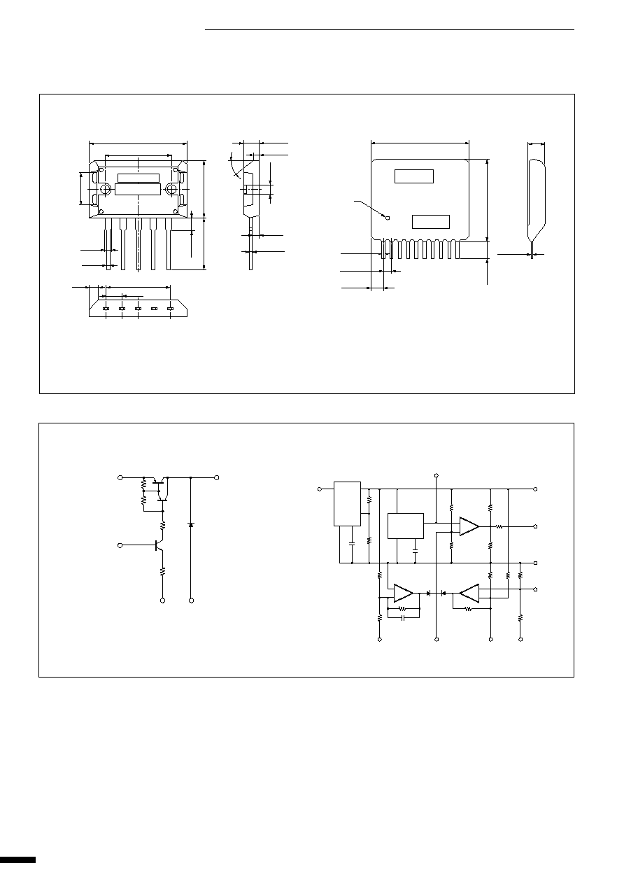
Outline Drawing
q
SW
OUT
(backside of case)
w
F
ly
W
heel
(ground)
e
Drive
r
V
IN
t
GND
Plastic Mold Package
Flammability: UL94V-0
Weight: Approx. 14.5g
Plastic Mold Package
(powder coating)
Weight: Approx. 3.4g
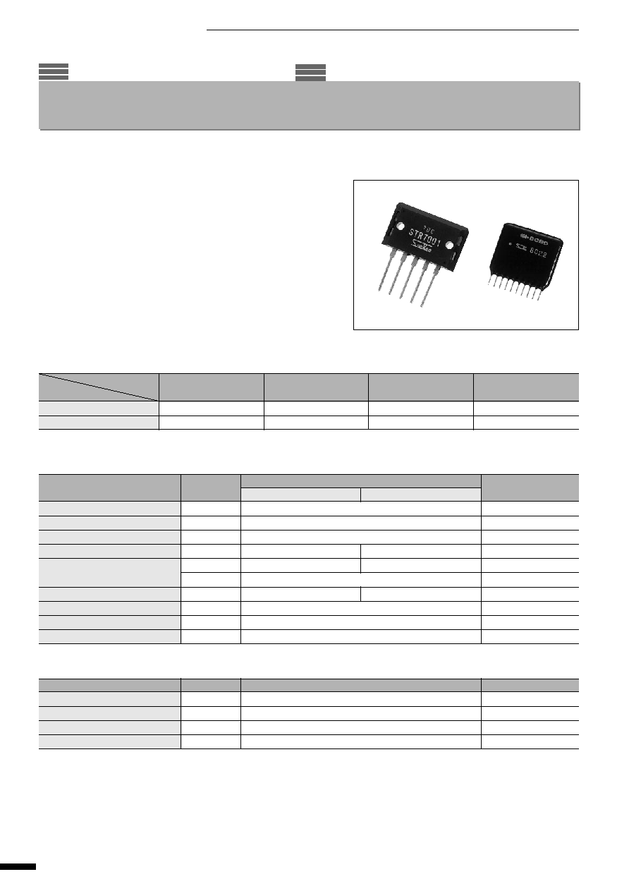
STR7000/7100 Series
SI-8020 Series
s
Block Diagram
STR7000/7100 Series
SI-8020 Series
V
IN
DRIVE
GND
F.WHEEL
SW.OUT
4
3
5
2
1
V
IN
10
7 V
REF
5 DRIVE
1 GND
2 V
O ADJ
3 V
O
.SENSE
6
8
4
COMPENSATION. B
COMPENSATION. A
CURR.SENSE
OSC.OUT SHUT DOWN
PWM COMP
V
O
AMP
I
O
AMP
VOLTAGE
REFERENCE
and
REGULATOR
9
+
≠
+
≠
+
≠
DEAD TIME
CONTROLLED
RAMP
GENERATOR
q
STR7000+SI-8020 Series
(unit: mm)
36.0
±
0.3
2.0
±
0.2
24.4
±
0.2
5.45
◊
4
2.0
3.0
30
∞
3.5
5.45
1.0
+0.2
≠0.1
0.6
+0.2
≠0.1
12.0
±
0.3
21.2
±
0.3
3.2
±
0.1
4.7
max.
6.0
max.
20.0
min.
q
w
e
r
t
Lot Number
Part Number
6
max.
30
max.
1 Pin
DOT
25
max.
0.27
±
0.05
0.5
±
0.05
2.54
±
0.1
7
max.
1
2
3
4
5
6
7
8
9 10
4.5
±
1.0
Part Number
Lot Number
89
s
Standard External Circuit
s
Notes of Pattern Design
1) Thick lines in the Standard External Circuit are lines through which a large current flows. Make these pattern lines as thick as possible.
2) Place capacitor C
1
on the input side as closely as possible to terminals no.2 and no.4 of the STR7000/7100 series. C
1
may be used in
combination with a smoothing capacitor for rectifying, but the above points must be taken into consideration. In cases where C
1
is not provided
or it is placed too far from the terminals stated above, abnormal oscillation due to poorer transient response or increased ringing may occur.
3) Connect voltage sensing terminal V
O.S
and GND as closely as possible to output capacitor C
4
(a current of approximately 1mA flows into the
V
O.S
terminal). If they are placed too far from C
4
, abnormal oscillation due to decreased regulation or increased switching ripple may occur.
4) Connect current sensing terminal C.S and GND as closely as possible to the detection resistor Rs (a current of approximately 0.5mA flows
from the CS terminal).
If they are placed too far from Rs, a decrease of the overcurrent setting point due to the voltage drop in the pattern, or malfunction of the
protection circuit due to increased ringing may occur.
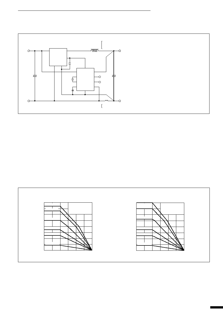
s
T
a
-P
D
Characteristics
STR7000 Series
STR7100 Series
3
2
9
4
V
IN
C
1
C
5
330P
C
2
330p
C
3
10
µ
F
2200
µ
F
C
4
1500
µ
F
◊
2 (parallel)
V
O
GND
*
C
5
STR7100 Series only
1
2
5
5
1
10
8
6
7
3
4
V
IN
GND
F/W
DRIVE
STR7000
STR7100
SERIES
SW
V
IN
V
O.S
R
S
V
O
. ADJ
OSC. OUT
SHUT DOWN
V
REF
C.S
C.A
C.B
GND
DRIVE
L
*
6A ... 0.02
12A ... 0.01
5V ... 200
µ
H
12V ...
250
µ
H
15V
24V ... 300
µ
H
SI-8020
SERIES
40
35
30
25
20
15
10
5
0
≠20
0
25
50
75
100
125
Power Dissipation P
D
(W)
Ambient Temperature T
a
(
∞
C)
200
◊
300
◊
2
200
◊
200
◊
2
100
◊
200
◊
2
100
◊
100
◊
2
75
◊
75
◊
2
Without heatsink
Without Mica
With Silicon Grease
Heatsink: Aluminum
Unit: mm
40
35
30
25
20
15
10
5
0
≠20
0
25
50
75
100
125
Power Dissipation P
D
(W)
Ambient Temperature T
a
(
∞
C)
200
◊
300
◊
2
200
◊
200
◊
2
100
◊
200
◊
2
100
◊
100
◊
2
75
◊
75
◊
2
Without heatsink
Without Mica
With Silicon Grease
Heatsink: Aluminum
Unit: mm
q
STR7000+SI-8020 Series
90
s
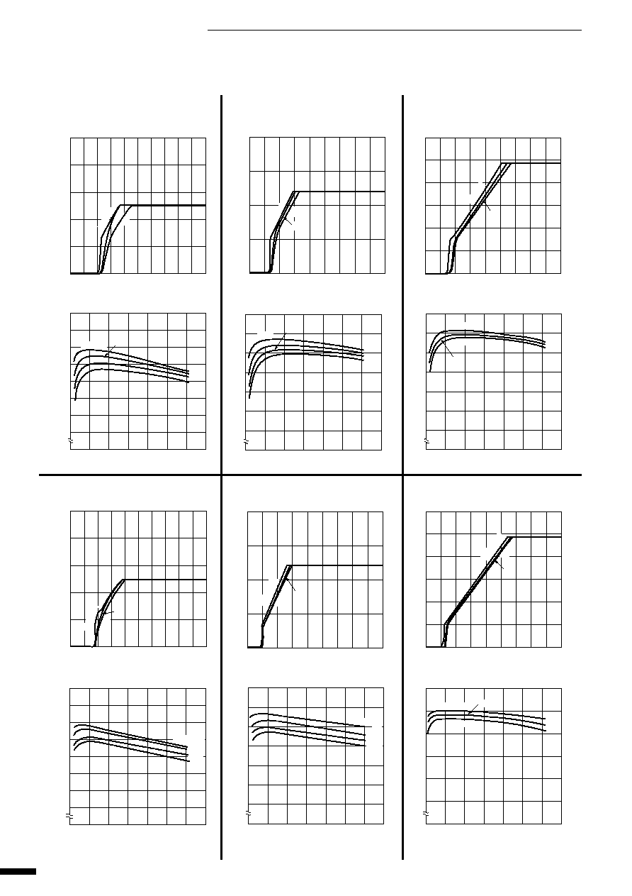
Typical Characteristics
STR7001+SI-8020(5V)
STR7002+SI-8021(12V)
STR7003+SI-8023(24V)
Rise Characteristics
Rise Characteristics
Rise Characteristics
Efficiency Characteristics
Efficiency Characteristics
Efficiency Characteristics
0
10
8
6
4
2
0
2
4
6
8
10
12
14
16
18
20
Input Voltage V
IN
(V)
Output Voltage V
O
(V)
I
O
=0.1A
3A
6A
100
90
80
70
60
50
40
30
0
0
1
2
3
4
5
6
7
Output Current I
O
(A)
Efficiency
(%)
V
IN
=11V
20V
30V
40V
0
5
10
15
20
25
30
35
40
45
I
O
=0.1A
6A
20
15
10
5
0
Input Voltage V
IN
(V)
Output Voltage V
O
(V)
3A
100
90
80
70
60
50
40
0
0
1
2
3
4
5
6
7
V
IN
=18V
30V
40V
50V
Output Current I
O
(A)
Efficiency
(%)
0
5
10
15
20
25
30
35
40
45
Input Voltage V
IN
(V)
3A
I
O
=0.1A
6A
30
25
20
15
10
5
0
Output Voltage V
O
(V)
100
90
80
70
60
50
40
0
0
1
2
3
4
5
6
7
V
IN
=30V
40V
50V
Output Current I
O
(A)
Efficiency
(%)
0
15
5
10
20
25
30
45
40
35
30
25
20
15
10
5
0
Input Voltage V
IN
(V)
Output Voltage V
O
(V)
lo=0.1 A12 A
0
6
2
4
8
10
12
14
100
90
80
70
60
50
0
Output Current I
O
(A)
Efficiency
(%)
V
IN
=30V
40V
50V
STR7101+SI-8020(5V)
STR7102+SI-8021(12V)
STR7103+SI-8023(24V)
Rise Characteristics
Rise Characteristics
Rise Characteristics
Efficiency Characteristics
Efficiency Characteristics
Efficiency Characteristics
0
2
4
6
8
10
12
14
16
18
20
10
8
6
4
2
0
Input Voltage V
IN
(V)
Output Voltage V
O
(V)
l
O
=0.1 A
6 A
12 A
0
6
2
4
8
10
12
14
100
90
80
70
60
50
40
30
0
Output Current I
O
(A)
Efficiency
(%)
VIN=11V
20V
30V
40V
0
20
5
10
15
25
30
35
45
40
20
15
10
5
0
Input Voltage V
IN
(V)
Output Voltage V
O
(V)
lo=0.1 A
6 A
12 A
0
6
2
4
8
10
12
14
100
90
80
70
60
50
40
0
Output Current I
O
(A)
Efficiency
(%)
V
IN
=18V
30V
40V
50V
(T
a
=25
∞
C)
q
STR7000+SI-8020 Series