SanRex 50 Seaview Blvd. Port Washington, NY 11050-4618 PH.(516)625-1313 FAX(516)625-8845 E-mail: semi@sanrex.com
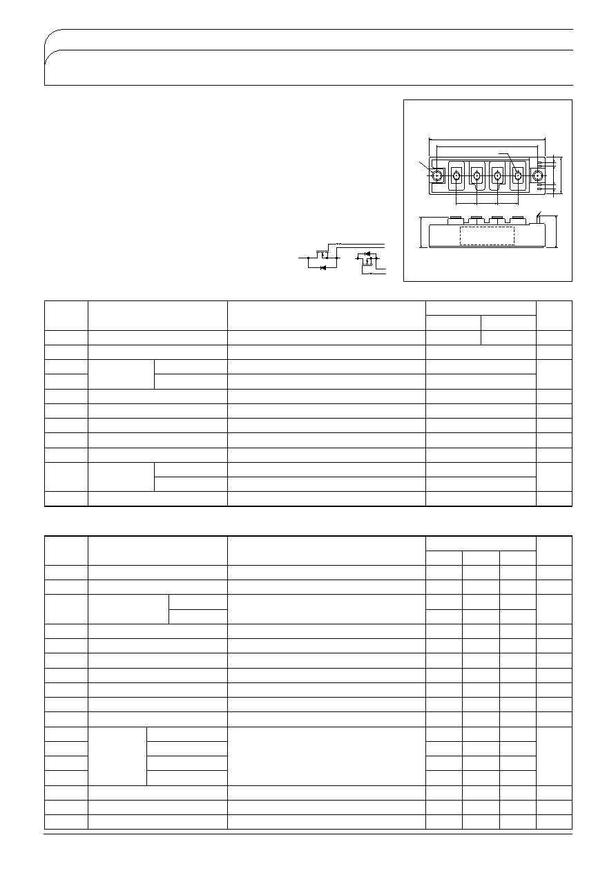
FBA75CA45/50
MOSFET MODULE
UL;E76102
M
FBA75CA45/50 is a dual power MOSFET module designed for fast swiching
applications of high voltage and current.
2 devices are serial connected. The
mounting base of the module is electrically isolated from semiconductor elements for
simple heatsink construction.
I
D
75A, V
DSS
500V
Suitable for high speed switching applications.
Low ON resistance.
Wide Safe Operating Areas.
Applications
UPS
CVCF
, Motor Control, Switching Power Supply, etc.
107.5
±
0.6
19
1
4
3
2
19
19
NAME PLATE
2
-
6.5
93
±
0.3
35
±
0.6
31max
30max
4
-
M5
8
4
17
4
7
6
5
TAB
=
110
T0.5
Unit
A
Maximum Ratings
Tj25 unless otherwise specified
Symbol
Item
Conditions
Ratings
FBA75CA45 FBA75CA50
Unit
V
DSS
Drain-Source Voltage
450
500
V
V
GSS
Gate-Source Voltage
±20
V
I
D
Drain
Current
D.C.
Pulse
Duty
36%
75
A
I
DP
150
-I
D
Source Current
75
A
P
T
Total Power Dissipation
Tc
25
400
W
Tj
Channel Temperature
150
Tstg
Storage Temperature
-40 to 125
V
ISO
Isolation Voltage
R.M.S.
A.C. 1minute
2500
V
Mounting
Torque
Mounting
M6
Terminal
M5
Recommended Value 2.5-3.9
25-40
4.7
48
N
m
kgfB
Recommended Value 1.5-2.5
15-25
2.7
28
Mass
Typical Value
220
g
q
D2 S1
D1
G2
S2
S1
G1
S2
S1
i
u
y
t
w e
r
Electrical Characteristics
Tj25 unless otherwise specified
Symbol
Item
Conditions
Ratings
Min.
Typ.
Max.
±1.0
Unit
I
GSS
Gate Leakage Current
V
GS
±20VV
DS
0V
A
1.0
I
DSS
Zero Gate Voltage Drain Current
V
GS
0VV
DS
500V
mA
450
V
BR
DSS
Drain-Source
Breakdown Voltage
FBA75CA45
FBA75CA50
V
GS
0VI
D
1mA
V
500
1.0
5.0
V
GS
th
Gate-Source Threshold Voltage
V
DS
V
GS
I
D
10mA
V
0.10
R
DS
on
Drain-Source On-State Resistance
I
D
40AV
GS
15V
4.0
V
DS
on
Drain-Source On-State Voltage
I
D
40AV
GS
15V
V
40
gfs
Forward Transconductance
V
DS
10VV
D
40A
S
13500
Ciss
Input Capacitance
V
GS
0VV
DS
25Vf1.0MHz
pF
2500
Coss
Output Capacitance
V
GS
0VV
DS
25Vf1.0MHz
pF
1000
Crss
Reverse Transfer Capacitance
V
GS
0VV
DS
25Vf1.0MHz
pF
60
tr
Switching
Time
Rise Time
Turn-on Delay Time
Fall Time
Turn-off Delay Time
R
L
7.5R
GS
50V
GS
15V
I
D
40AR
G
5
ns
120
td
on
700
tf
210
td
off
1.5
V
SDS
Diode Forward Voltage
I
D
40AV
GS
0V
V
700
trr
Reverse Recovery Time
I
D
40AV
GS
0Vdi/dt100A/s
ns
0.31
Rth
j-c Thermal Resistance
/W
50 Seaview Blvd. Port Washington, NY 11050-4618 PH.(516)625-1313 FAX(516)625-8845 E-mail: semi@sanrex.com
FBA75CA45/50
Tj
25
V
GS
4V
Pulse Test
5V
6V
8V
10V
15V
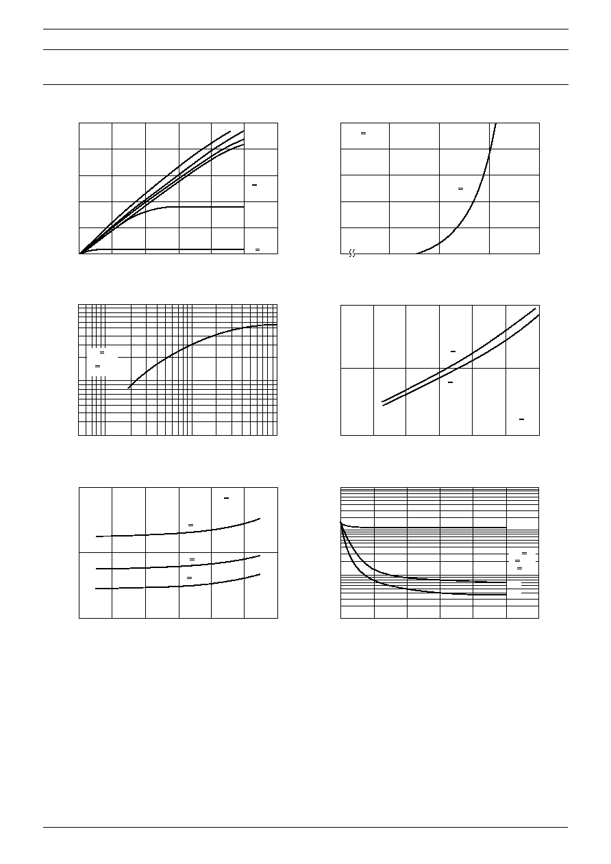
Output CharacteristicsTypical
Drain Current I
D
A
Drain-Source Voltage V
V
Tj
25
V
DS
10V
Pulse Test
Forward Transfer CharacteristicsTypical
Drain Current I
D
A
Gate-Source Voltage V
V
Pulse Test
V
DS
10V
Tj
25
(Typical)
Forward Transconductance Vs.
Drain Current
Drain Current
A
0
Forward Transconductance
S
Pulse Test
V
GS
10V
I
D
75A
I
D
37.5A
Drain-Source On-State Resistance Vs.
Channel Temperature
-
-
Channel Temperature
Drain-Source On-State Resistance
Pulse Test
V
GS
10V
Tj
25
Tj
100
Tj
-25
Drain Current
A
Drain-Source On-State Resistance Vs.
Drain Current
Drain-Source On-State Resistance
Ciss
V
GS
0V
f
1MHz
Tj
25
Coss
Crss
Input Capacitance, Output Capacitance,
Reverse Transfer CapacitanceTypical
Capacitance
Drain-Source Voltage V
DS
V
SanRex
Æ
50 Seaview Blvd. Port Washington, NY 11050-4618 PH.(516)625-1313 FAX(516)625-8845 E-mail: semi@sanrex.com
FBA75CA45/50
Pw
10
s
100
s
1m
s
10m
s
D.C.
FBA75CA45
FBA75CA50
Safe Operating Area
Drain Current I
D
A
Drain-Source Voltage V
V
-
1
1
0
Tj
25
(Typical)
Pulse Test
Forward Voltage of Free Wheeling Diode
Source Current
I
S
A
Source-Drain Voltage V
V
Max.
50msec
-
10sec
50sec
-
50msec
Max.
Transient Thermal Impedance
Thermal Impedance
-
/
-
-
Time
sec
D
0.5
0.2
0.1
0.05
0.02
0.01
0
Normalized Transient Thermal Impedanse
Vs. Pulse Width
Pulse
sec
Normalized Transient Thermal Impedanse
/
SanRex
Æ