SanRex 50 Seaview Blvd. Port Washington, NY 11050-4618 PH.(516)625-1313 FAX(516)625-8845 E-mail: semi@sanrex.com
PK
(PD,PE)
40FG
THYRISTOR MODULE
Symbol
Item
Conditions
Ratings
40
Unit
I
T
AV
Average On-state Current
I
T
RMS
R.M.S. On-state Current
Single phase, half wave, 180
∞conduction, Tc83
Single phase, half wave, 180
∞conduction, Tc83
I
TSM
Surge On-state Current
I
2
t
I
2
t
P
GM
Peak Gate Power Dissipation
P
G
AV
Average Gate Power Dissipation
I
FGM
Peak Gate Current
V
FGM
Peak Gate Voltage (Forward)
1
2
Cycle, 50/60H
Z
, Peak Value, non-repetitive
Value for one cycle surge current
A
62
A
870/950
A
3760
10
A
2
S
W
1
V
RGM
Peak Gate Voltage (Reverse)
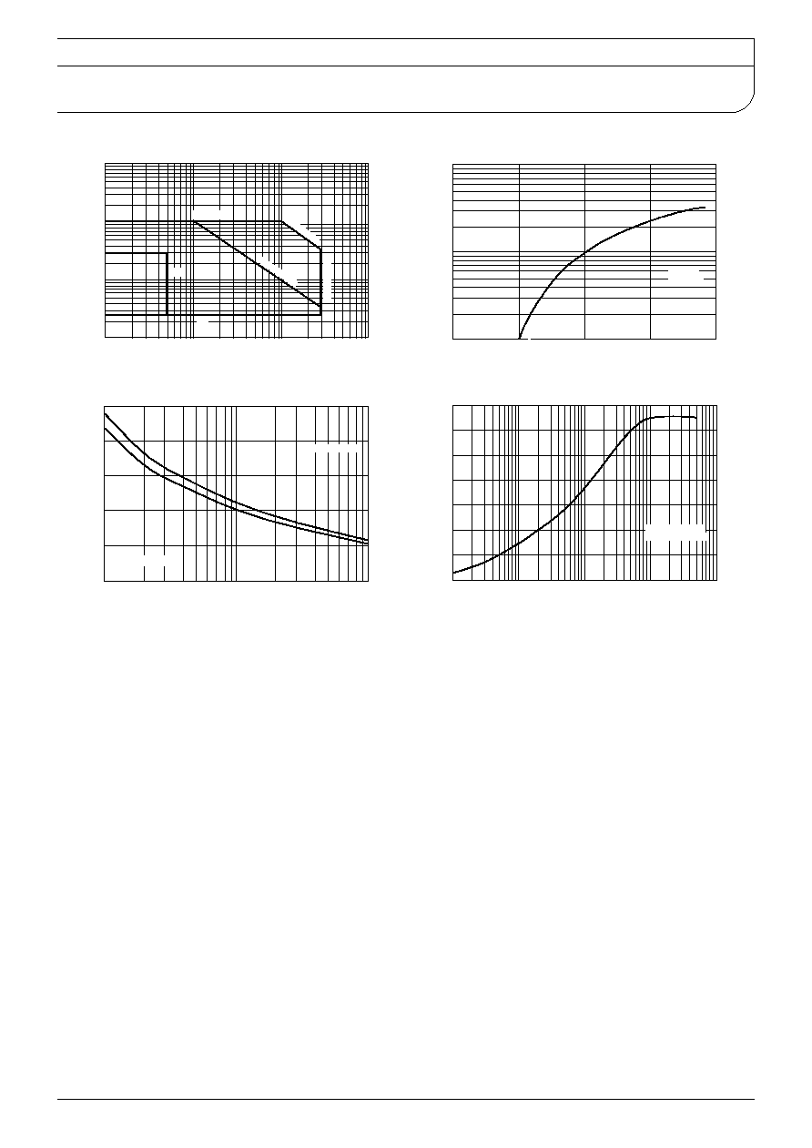
di/dt
Critical Rate of Rise of On-state Current
I
G
100mA
V
D
1
2
V
DRM
di
G
/dt0.1A/s
Tj
Operating Junction Temperature
Tstg
Storage Temperature
Mounting
Torque
Mounting
M5
Terminal
M5
Mass
Recommended Value 1.5-2.5
15-25
Recommended Value 1.5-2.5
15-25
Typical Value
3
W
A
10
V
5
V
100
A/
s
-40 to 125
V
ISO
Isolation Breakdown VoltageR.M.S.
A.C. 1minute
2500
V
-40 to 125
2.7
28
2.7
28
170
N
m
fB
g
Symbol
Item
Conditions
Ratings
10
Unit
I
DRM
Repetitive Peak off-state Current,max
I
RRM
Repetitive Peak Reverse Current,max
Tj
125V
D
V
DRM
Tj
125V
D
V
DRM
V
TM
On-state Voltage,max
I
GT
Gate Trigger Current,max
V
GD
Gate Non-Trigger Voltage,min
dv/dt
Critical Rate of Rise of off-state Voltage,min
I
T
120A
V
D
6VI
T
1A
mA
10
mA
1.6
V
50
Tj
125V
D
1
2
V
DRM
0.25
mA
V
GT
Gate Trigger Voltage,max
V
D
6VI
T
1A
3
V
V
Tj
125V
D
2
3
V
DRM
Rth
j-cThermal Impedance,max
Junction to case
1000
V/
s
0.65
/W
Electrical Characteristics
Maximum Ratings
Tj25 unless otherwise specified
92
2
2
2
±
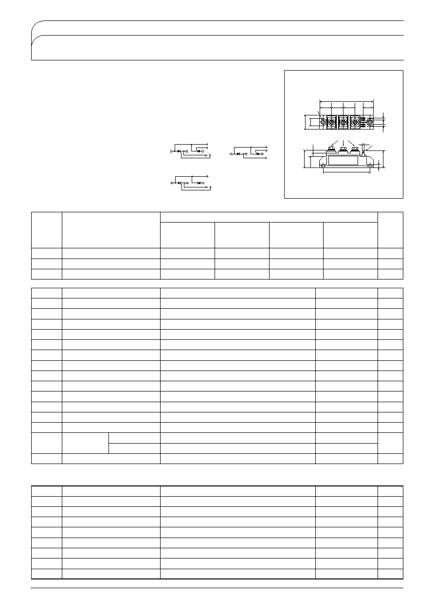
NAME PLATE
M◊1
±
MAX
3
5
5
4-TAB
-6
K
G
K
G
Unit
A
I
T(AV)
40A, I
T(RMS)
62A, I
TSM
950A
di/dt 100A/
s
dv/dt 1000V/
s
Applications
Various rectifiers
AC/DC motor drives
Heater controls
Light dimmers
Static switches
Internal Configurations
Power Thyristor/Diode Module PK40FG series are designed for various rectifier circuits
and power controls. For your circuit application, following internal connections and wide
voltage ratings up to 1600V are available. and electrically isolated mounting base make
your mechanical design easy.
Symbol
Item
PK40FG40
PD40FG40
PE40FG40
Ratings
PK40FG120
PD40FG120
PE40FG120
Unit
V
RRM
Repetitive Peak Reverse Voltage
400
1200
V
480
1300
V
400
PK40FG80
PD40FG80
PE40FG80
800
960
800
1200
PK40FG160
PD40FG160
PE40FG160
1600
1700
1600
V
V
RSM
V
DRM
Non-Repetitive Peak Reverse Voltage
Repetitive Peak off-state Voltage
markThyristor and Diode part. No markThyristor part
UL;E76102
M
K1
A2
K2
A1K2
G1
K2
G2
1
2
3
PK
K1
A2
K2
A1K2
K2
G2
1
2
3
PE
K1
A2
K2
A1K2
G1
K2
1
2
3
PD