2SC5417
Ordering number : EN5817
Inverter Lighting Applications
NPN Triple Diffused Planar Silicon Transistor
SANYO Electric Co.,Ltd. Semiconductor Bussiness Headquarters
TOKYO OFFICE Tokyo Bldg., 1-10, 1 Chome, Ueno, Taito-ku, TOKYO, 110-8534 JAPAN
51598TS (KOTO) TA-1043 No.5817-1/4
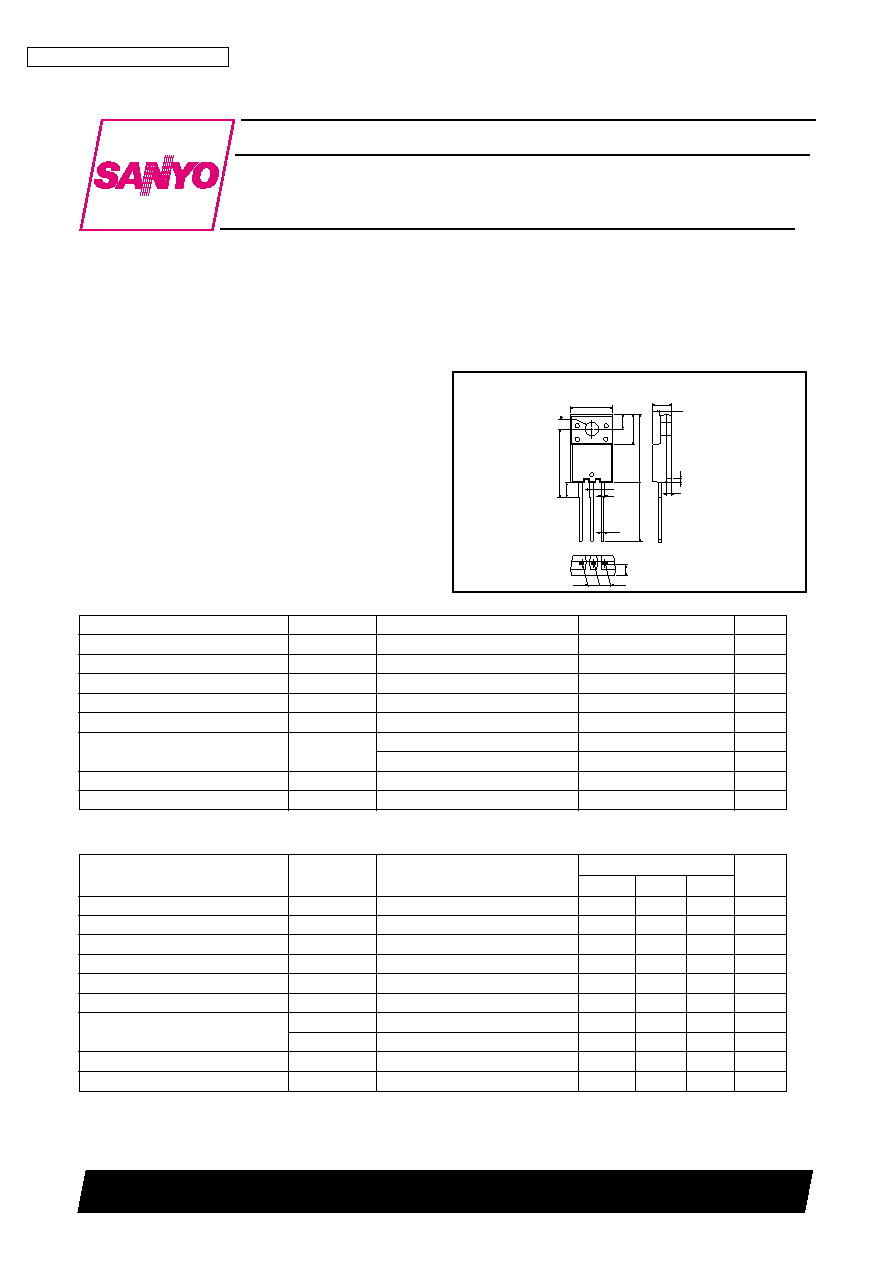
Package Dimensions
unit: mm
2079B-TO220FI (LS)
[2SC5417]
SANYO : TO220FI (LS)
1 : Base
2 : Collector
3 : Emitter
3.5
7.2
16.0
16.1
3.6
10.0
0.9
1.2
14.0
0.75
4.5
2.8
0.6
0.7
2.4
2.55
2.55
1
2
3
3.2
Specifications
Absolute Maximum Ratings
at Ta=25∞C
Parameter
Symbol
Conditions
Ratings
Unit
Collector-to-Base Voltage
VCBO
1200
V
Collector-to-Emitter Voltage
VCEO
600
V
Emitter-to-Base Voltage
VEBO
9
V
Collector Current
IC
3
A
Collector Current (Pulse)
ICP
6
A
Collector Dissipation
PC
2
W
Tc=25∞C
25
W
Junction Temperature
Tj
150
∞C
Storage Temperature
Tstg
≠55 to +150
∞C
Electrical Characteristics
at Ta=25∞C
Parameter
Symbol
Conditions
Ratings
min
typ
max
Unit
Collector Cutoff Current
ICBO
VCB=600V, IE=0
10
µA
Collector Cutoff Current
ICES
VCE=1200V, RBE=0 1.0
mA
Collector Sustain Voltage
VCEO(sus)
IC=100mA, IB=0
600
V
Emitter Cutoff Current
IEBO
VEB=9V, IC=0
1.0
mA
C-E Saturation Voltage
VCE(sat)
IC=1.5A, IB=0.3A
1.0
V
B-E Saturation Voltage
VBE(sat)
IC=1.5A, IB=0.3A
1.5
V
DC Current Gain
hFE(1)
VCE=5V, IC=0.1A
30
40
50
hFE(2)
VCE=5V, IC=1.0A
10
Storage Time
tstg
IC=1.5A, IB1=0.3A, IB2=≠0.6A
2.5
µs
Fall Time
tf
IC=1.5A, IB1=0.3A, IB2=≠0.6A
0.15
µs
Features
∑ High breakdown voltage.
∑ High reliability (Adoption of HVP process).
∑ Adoption of MBIT process.

Switching Time Test Circuit
2SC5417
No.5817-2/4
IB1
IB2
VOUT
RC
VCC
IB1
0.1 VOUT
IB2
VOUT
tstg tf
0.9 VOUT
D
C
C
u
r
r
e
n
t
G
a
i
n
,
h
F
E
Collector Current,I
C
≠ A
Collector Current,I
C
≠ A
C
o
l
l
e
c
t
o
r
C
u
r
r
e
n
t
,
I
C
≠
A
h
FE
≠ I
C
Collector-to-Emitter Voltage, V
CE
≠ V
I
C
≠ V
CE
C
o
l
l
e
c
t
o
r
C
u
r
r
e
n
t
,
I
C
≠
A
I
C
≠ V
BE
V
CE
(
sat
)
≠ I
C
Collector Current,I
C
≠ A
Base-to-Emitter Voltage, V
BE
≠ V
C
o
l
l
e
c
t
o
r
-
t
o
-
E
m
i
t
t
e
r
S
a
t
u
r
a
t
i
o
n
V
o
l
t
a
g
e
,
V
C
E
(
s
a
t
)
≠
V
V
BE
(
sat
)
≠ I
C
Collector Current,I
C
≠ A
B
a
s
e
-
t
o
-
E
m
i
t
t
e
r
S
a
t
u
r
a
t
i
o
n
V
o
l
t
a
g
e
,
V
B
E
(
s
a
t
)
≠
V
S
w
i
t
c
h
i
n
g
T
i
m
e
,
S
W
T
i
m
e
≠
µ
s
SW Time ≠ I
C
S
0
0
1
2
3
4
5
6
7
8
9
10
1
2
3
5
4
0
0
0.2
0.4
0.6
0.8
1.0
1.2
1.4
1
2
3
4
1.0
0.01
0.1
1.0
10
7
2
3
5
100
7
2
3
5
7
2
3
5 7
2
3
5
2
3
5
7
1.0
10
2
3
5
2
3
5
7
7
0.1
2
3
0.01
5
7
0.01
0.1
1.0
7
2
3
5
7
2
3
5
2
3
5
7
0.1
0.01
0.1
1.0
1.0
7
2
3
5
2
3
5
7
10
7
2
3
5 7
2
3
5
2
3
5
7
0.1
1.0
7
2
3
5
7
2
3
5
1.0
10
2
3
5
5
2
3
5
7
7
0.1
7
I
B
= 0
V
CE
=5V
V
CC
= 200V
I
C
/
I
B1
=5
I
B2
/ I
B1
=2
R
load
T
a=
1
2
0
∞
C
2
5
∞
C
≠
4
0
∞
C
25
∞
C
≠40
∞
C
≠4
0
∞
C
25
∞
C
T
a=
1
2
0
∞
C
Ta=120
∞
C
t
f
t
stg
2.0A
0.2A
0.4A
0.6A
0.8A
1.0A
1.2A
1.8A
0.05A
0.1A
1.4A
1.6A
V
CE
=5V
I
C
/
I
B
=5
I
C
/
I
B
=5
120
∞
C
Ta=≠40
∞
C
25
∞
C

2SC5417
No.5817-3/4
Collector-to-Emitter Voltage, V
CE
≠ V
Base Current, I
B2
≠ A
S
w
i
t
c
h
i
n
g
T
i
m
e
,
S
W
T
i
m
e
≠
µ
s
Forward Bias A S O
SW Time ≠ I
B2
C
o
l
l
e
c
t
o
r
C
u
r
r
e
n
t
,
I
C
≠
A
0.1
1.0
7
2
3
5
7
2
3
1.0
2
3
5
5
7
10
2
3
5
7
0.1
7
10
100
0.01
5
7
0.1
2
3
5
2
3
5
2
3
5
7
1.0
7
10
7
5
7
2
3
5
7
1000
2
3
2
3
5
7
PT
<
50
µ
s
V
CC
=200V
I
C
=1.5A
I
B1
=0.3A
R
load
t
f
t
stg
I
C
I
CP
10
0
µ
s
30
0
µ
s
1m
s
10
m
s
D
C
o
pe
ra
tio
n
Tc=25
∞
C
1Pulse
C
o
l
l
e
c
t
o
r
D
i
s
s
i
p
a
t
i
o
n
,
P
C
≠
W
C
o
l
l
e
c
t
o
r
D
i
s
s
i
p
a
t
i
o
n
,
P
C
≠
W
80
100
120
140
160
60
40
20
0
80
100
120
140
160
60
40
20
0
0
10
20
25
30
0
1
2
3
Ambient Temperature, Ta ≠
∞
C
Case Temperature, Tc ≠
∞
C
P
C
≠ Ta
P
C
≠ Tc
0.1
2
3
5
1.0
7
2
3
5
10
7
100
5
7
1000
2
3
5
2
3
7
Collector-to-Emitter, V
CE
≠ V
Reverse Bias A S O
C
o
l
l
e
c
t
o
r
C
u
r
r
e
n
t
,
I
C
≠
A
No
he
at s
ink
L=200
µ
H
I
B2
=≠1A
Tc=25
∞
C
1 pulse

2SC5417
No.5817-4/4
No products described or contained herein are intended for use in surgical implants, life-support systems,
aerospace equipment, nuclear power control systems, vehicles, disaster/crime-prevention equipment and
the like, the failure of which may directly or indirectly cause injury, death or property loss.
Anyone purchasing any products described or contained herein for an above-mentioned use shall:
Accept full responsibility and indemnify and defend SANYO ELECTRIC CO., LTD., its affiliates,
subsidiaries and distributors and all their officers and employees, jointly and severally, against any
and all claims and litigation and all damages, cost and expenses associated with such use:
Not impose any responsibilty for any fault or negligence which may be cited in any such claim or
litigation on SANYO ELECTRIC CO., LTD., its affiliates, subsidiaries and distributors or any of
their officers and employees jointly or severally.
Information (including circuit diagrams and circuit parameters) herein is for example only; it is not guarant-
eed for volume production. SANYO believes information herein is accurate and reliable, but no guarantees
are made or implied regarding its use or any infringements of intellectual property rights or other rights of
third parties.
This catalog provides information as of May, 1998. Specifications and information herein are subject to
change without notice.