 | –≠–ª–µ–∫—Ç—Ä–æ–Ω–Ω—ã–π –∫–æ–º–ø–æ–Ω–µ–Ω—Ç: 2SC5645 | –°–∫–∞—á–∞—Ç—å:  PDF PDF  ZIP ZIP |
2SC5645
No.6588-1/6
UHF to S Band Low-Noise Amplifier
and OSC Applications
Features
∑
Low noise : NF=1.5dB typ (f=2GHz).
∑
High cutoff frequency : fT=10GHz typ (VCE=1V).
: fT=12.5GHz typ (VCE=3V).
∑
Low-voltage operating .
∑
High gain :
S21e
2
=9.5dB typ (f=2GHz).
Specifications
Absolute Maximum Ratings
at Ta=25
∞
C
Parameter
Symbol
Conditions
Ratings
Unit
Collector-to-Base Voltage
VCBO
9
V
Collector-to-Emitter Voltage
VCEO
4
V
Emitter-to-Base Voltage
VEBO
2
V
Collector Current
IC
30
mA
Collector Dissipation
PC
100
mW
Junction Temperature
Tj
150
∞
C
Storage Temperature
Tstg
--55 to +150
∞
C
Electrical Characteristics
at Ta=25
∞
C
Ratings
Parameter
Symbol
Conditions
min
typ
max
Unit
Collector Cutoff Current
ICBO
VCB=5V, IE=0
1.0
µ
A
Emitter Cutoff Current
IEBO
VEB=1V, IC=0
10
µ
A
DC Current Gain
hFE
VCE=1V, IC=5mA
100
160
Gain-Bandwidth Product
fT1
VCE=1V, IC=5mA
8
10
GHz
fT2
VCE=3V, IC=15mA
12.5
GHz
Output Capacitance
Cob
VCE=1V, f=1MHz
0.55
0.7
pF
Reverse Transfer Capacitance
Cre
VCE=1V, f=1MHz
0.4
pF
Forward Transfer Gain
S21e
2
1
VCE=1V, IC=5mA, f=2GHz
8
9.5
dB
S21e
2
2
VCE=3V, IC=15mA, f=2GHz
10.5
dB
Noise Figure
NF
VCE=1V, IC=3mA, f=2GHz
1.5
2.3
dB
Marking : NF
SANYO Electric Co.,Ltd. Semiconductor Company
TOKYO OFFICE Tokyo Bldg., 1-10, 1 Chome, Ueno, Taito-ku, TOKYO, 110-8534 JAPAN
2SC5645
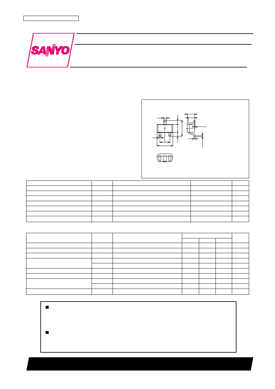
Package Dimensions
unit : mm
2106A
[2SC5645]
90100 TS IM TA-3001
Any and all SANYO products described or contained herein do not have specifications that can handle
applications that require extremely high levels of reliability, such as life-support systems, aircraft's
control systems, or other applications whose failure can be reasonably expected to result in serious
physical and/or material damage. Consult with your SANYO representative nearest you before using
any SANYO products described or contained herein in such applications.
SANYO assumes no responsibility for equipment failures that result from using products at values that
exceed, even momentarily, rated values (such as maximum ratings, operating condition ranges, or other
parameters) listed in products specifications of any and all SANYO products described or contained
herein.
NPN Epitaxial Planar Silicon Transistor
1 : Base
2 : Emitter
3 : Collector
SANYO : SMCP
0.8
0.4
0.4
2
3
1.6
0.2
1.6
0.3
0.5 0.5
1
0.75
0.6
0 to 0.1
0.1
0.1max
Ordering number : ENN6588

2SC5645
No.6588-2/6
VCE=3V
1V
0
0
2
Collector-to-Emitter Voltage, VCE -- V
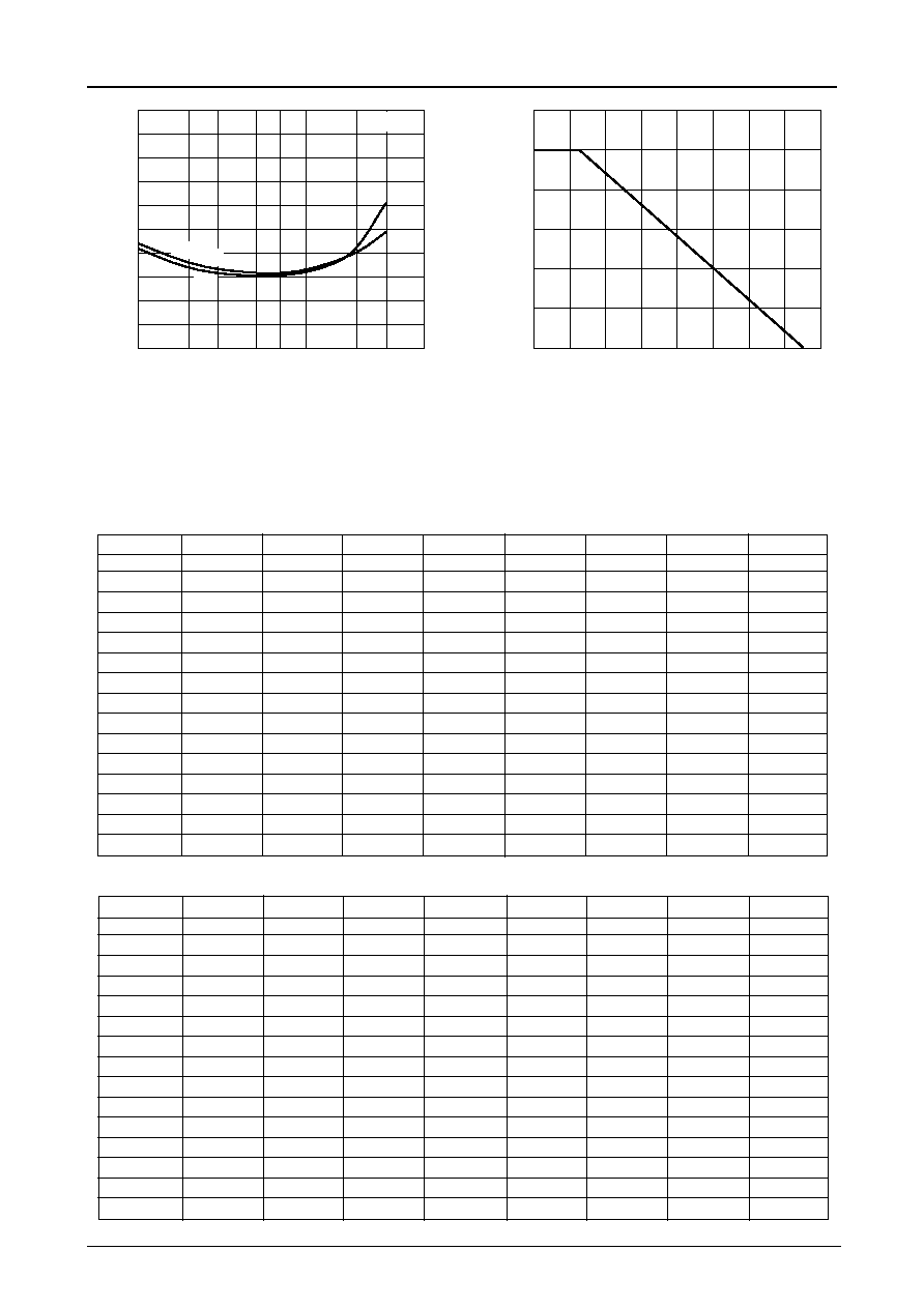
IC -- VCE
Collector Current, I
C
-
-
mA
IT02250
IT02252
IT02254
IT02251
IT02253
IT02255
4
6
8
10
1
3
2
4
5
0
0
Base-to-Emitter Voltage, VBE -- V
IC -- VBE
Collector Current, I
C
-
-
mA
0.2
0.4
0.6
0.8
1.0
1.2
20
30
10
10
Collector Current, IC -- mA
hFE -- IC
DC Current Gain, h
FE
1.0
2
3
5
7
3
5
7
2
3
5
7
10
100
100
2
3
5
1000
7
2
3
5
7
1.0
Collector Current, IC -- mA
f T -- IC
Gain-Bandwidth Product, f
T
-
-
GHz
2
3
5
7
10
2
3
5
7
100
1.0
2
3
5
7
2
3
5
7
100
10
0.1
0.1
Collector-to-Base Voltage, VCB -- V
Cob -- VCB
Output Capacitance, Cob -
-
pF
1.0
2
3
5
7
2
3
5
7
10
2
3
5
7
1.0
0.1
Collector-to-Base Voltage, VCB -- V
Cre -- VCB
Re
v
erse
T
ransfer Capacitance, Cre -
-
pF
2
3
5
7
2
3
5
7
1.0
10
0.1
2
3
5
7
1.0
IB=0
0.05mA
0.04mA
0.03mA
0.02mA
0.01mA
V
CE
=3V
1V
VCE=3V
1V
VCE=3V
1V
f=1MHz
f=1MHz
IT02256
IT02257
S21e
2
-- IC
1.0
Collector Current, IC -- mA
S21e
2
-- IC
F
orw
ard T
ransfer
Gain,
S21e
2
-
-
dB
2
3
5
7
2
3
5
7
10
100
0
2
4
6
8
18
16
14
12
10
1.0
Collector Current, IC -- mA
F
orw
ard T
ransfer
Gain,
S21e
2
-
-
dB
10
2
3
5
7
2
3
5
7
100
0
2
4
6
8
10
12
14
18
16
f=1GHz
VCE
=3V
1V
f=2GHz
2SC5645
No.6588-3/6
1.0
0
1.0
0.5
1.5
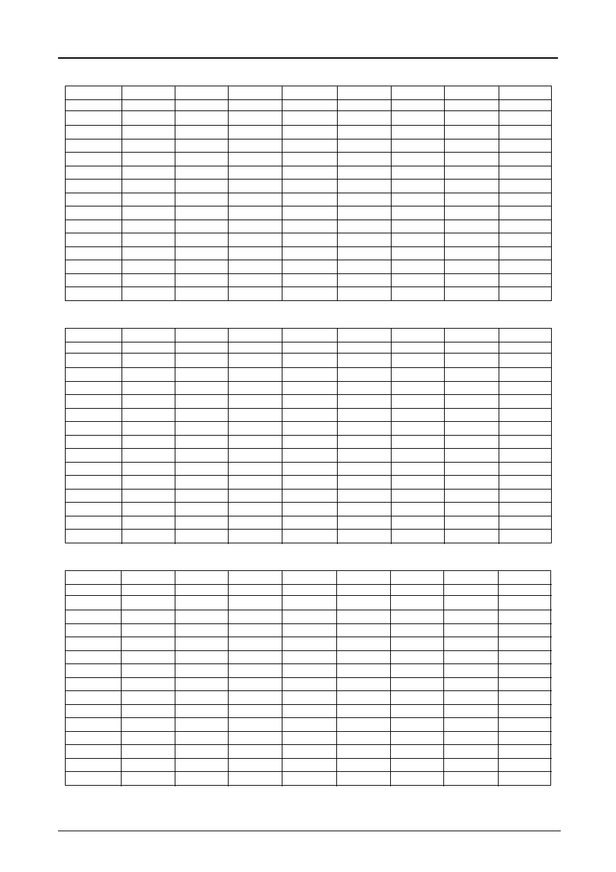
Collector Current, IC -- mA
NF -- IC
Noise Figure, NF
--
dB
IT02258
2.0
2.5
3.0
4.0
3.5
5.0
4.5
5
3
2
7
5
3
2
10
0
0
20
Ambient Temperature, Ta --
∞
C
PC -- Ta
Collector Dissipation, P
C
-
-
mW
IT02259
40
60
100
80
120
40
20
100
120
60
80
140
160
VCE=3V
1V
f=2GHz
S Parameters (Common emitter)
VCE=1V, IC=1mA, ZO=50
Freq(MHz)
S
11
S
11
S
21
S
21
S
12
S
12
S
22
S
22
200
0.971
--13.1
3.176
166.5
0.047
79.7
0.975
--10.2
400
0.939
--25.7
3.090
153.7
0.089
70.4
0.946
--19.8
600
0.872
--36.9
2.916
142.1
0.123
59.5
0.878
--28.0
800
0.806
--49.0
2.622
131.1
0.155
53.0
0.838
--36.8
1000
0.782
--59.2
2.581
121.1
0.179
47.6
0.798
--43.8
1200
0.711
--69.6
2.440
111.0
0.193
42.4
0.757
--49.3
1400
0.656
--78.1
2.242
102.3
0.210
38.1
0.721
--55.4
1600
0.617
--86.0
2.116
95.2
0.220
34.0
0.682
--60.1
1800
0.551
--93.3
1.997
86.9
0.224
31.4
0.660
--63.8
2000
0.537
--100.8
1.848
82.7
0.228
27.8
0.615
--68.1
2200
0.482
--108.2
1.816
74.4
0.233
27.4
0.620
--70.7
2400
0.472
--113.9
1.663
69.5
0.238
24.0
0.591
--76.3
2600
0.439
--122.5
1.647
63.6
0.236
24.0
0.574
--77.5
2800
0.425
--126.1
1.529
58.2
0.239
23.0
0.554
--80.4
3000
0.423
--134.7
1.523
53.3
0.247
24.2
0.588
--80.3
VCE=1V, IC=5mA, ZO=50
Freq(MHz)
S
11
S
11
S
21
S
21
S
12
S
12
S
22
S
22
200
0.828
--34.4
11.283
152.9
0.046
70.9
0.899
--25.1
400
0.701
--62.6
9.573
131.4
0.076
57.2
0.743
--44.4
600
0.599
--83.6
7.640
116.9
0.098
49.6
0.613
--57.0
800
0.522
--100.4
6.319
105.7
0.108
45.7
0.528
--65.6
1000
0.475
--112.6
5.241
98.5
0.119
44.0
0.458
--72.6
1200
0.436
--124.0
4.498
92.0
0.125
43.4
0.423
--76.9
1400
0.420
--132.7
3.954
86.0
0.131
44.9
0.404
--80.1
1600
0.401
--141.0
3.503
80.7
0.140
45.2
0.378
--83.7
1800
0.391
--147.6
3.186
75.8
0.148
45.6
0.369
--86.0
2000
0.387
--152.3
2.887
71.5
0.157
45.6
0.357
--88.6
2200
0.378
--158.0
2.663
67.2
0.168
45.3
0.353
--90.4
2400
0.377
--161.6
2.482
63.4
0.175
45.7
0.352
--94.5
2600
0.370
--166.2
2.298
59.8
0.181
46.2
0.329
--93.8
2800
0.365
--170.2
2.136
57.1
0.193
47.3
0.343
--89.8
3000
0.364
--172.7
2.045
54.0
0.206
46.9
0.400
--93.3

2SC5645
No.6588-4/6
VCE=1V, IC=10mA, ZO=50
Freq(MHz)
S
11
S
11
S
21
S
21
S
12
S
12
S
22
S
22
200
0.709
--49.8
15.927
143.7
0.043
64.8
0.811
--34.2
400
0.565
--84.6
11.658
121.5
0.064
52.7
0.605
--54.7
600
0.484
--107.0
8.751
107.8
0.078
49.2
0.477
--66.3
800
0.435
--123.1
6.913
98.8
0.086
49.8
0.397
--73.6
1000
0.408
--135.0
5.714
91.7
0.097
50.7
0.356
--79.1
1200
0.390
--144.5
4.851
86.1
0.107
50.7
0.327
--83.0
1400
0.386
--152.0
4.211
81.2
0.115
51.8
0.307
--86.6
1600
0.380
--158.3
3.720
76.6
0.128
52.3
0.296
--89.0
1800
0.377
--164.1
3.347
72.4
0.138
53.3
0.287
--91.6
2000
0.377
--168.0
3.040
68.5
0.148
53.4
0.289
--92.7
2200
0.373
--172.1
2.780
64.8
0.160
53.0
0.290
--94.2
2400
0.372
--175.7
2.571
61.5
0.173
53.1
0.295
--98.2
2600
0.367
--178.3
2.397
57.8
0.182
53.7
0.274
--97.0
2800
0.365
178.9
2.231
55.1
0.197
53.9
0.291
--91.5
3000
0.367
176.1
2.136
52.3
0.209
52.1
0.351
--95.0
VCE=1V, IC=20mA, ZO=50
Freq(MHz)
S
11
S
11
S
21
S
21
S
12
S
12
S
22
S
22
200
0.571
--71.7
17.704
133.8
0.038
60.1
0.677
--42.5
400
0.472
--110.6
11.551
112.1
0.053
51.3
0.465
--61.1
600
0.434
--132.2
8.287
100.3
0.065
52.2
0.359
--70.5
800
0.415
--145.7
6.393
92.4
0.076
54.2
0.303
--76.0
1000
0.405
--155.0
5.241
86.4
0.085
55.7
0.275
--80.7
1200
0.402
--162.7
4.397
81.2
0.096
57.3
0.258
--84.0
1400
0.404
--168.4
3.800
76.4
0.108
58.5
0.251
--86.9
1600
0.402
--173.4
3.349
72.2
0.122
58.8
0.249
--88.8
1800
0.403
--176.9
3.012
68.1
0.133
58.7
0.248
--92.0
2000
0.401
--179.8
2.722
64.5
0.145
58.7
0.253
--92.5
2200
0.401
176.6
2.498
60.9
0.158
58.4
0.264
--94.4
2400
0.404
173.7
2.297
57.8
0.169
57.9
0.272
--97.7
2600
0.401
171.4
2.151
54.3
0.182
58.6
0.254
--97.0
2800
0.396
169.5
2.012
51.8
0.199
58.0
0.273
--91.6
3000
0.400
167.2
1.919
48.9
0.211
56.0
0.337
--95.4
VCE=3V, IC=1mA, ZO=50
Freq(MHz)
S
11
S
11
S
21
S
21
S
12
S
12
S
22
S
22
200
0.978
--11.3
3.288
167.6
0.041
80.9
0.973
--8.8
400
0.951
--22.6
3.167
156.1
0.078
72.6
0.950
--17.2
600
0.898
--33.0
2.983
146.6
0.109
62.5
0.897
--24.6
800
0.837
--42.3
2.805
132.8
0.137
56.1
0.858
--32.8
1000
0.805
--53.1
2.683
123.8
0.160
51.5
0.828
--39.1
1200
0.748
--60.9
2.484
116.0
0.178
46.6
0.794
--44.1
1400
0.707
--68.6
2.299
107.5
0.192
41.9
0.758
--50.0
1600
0.653
--77.0
2.152
99.1
0.202
38.4
0.720
--54.7
1800
0.599
--82.1
2.028
93.8
0.211
34.6
0.698
--58.4
2000
0.570
--90.8
1.913
85.2
0.212
32.7
0.659
--62.2
2200
0.519
--94.9
1.830
80.7
0.223
30.6
0.660
--65.2
2400
0.510
--102.7
1.775
72.9
0.223
28.5
0.635
--70.2
2600
0.458
--108.1
1.659
68.4
0.229
27.1
0.614
--71.9
2800
0.462
--113.4
1.644
62.7
0.224
27.2
0.596
--74.0
3000
0.428
--119.8
1.568
56.7
0.241
28.1
0.630
--74.6
2SC5645
No.6588-5/6
VCE=3V, IC=5mA, ZO=50
Freq(MHz)
S
11
S
11
S
21
S
21
S
12
S
12
S
22
S
22
200
0.839
--31.1
11.349
155.2
0.040
70.9
0.916
--22.0
400
0.723
--56.3
9.627
135.7
0.070
61.0
0.787
--38.3
600
0.610
--77.4
8.210
119.8
0.087
51.7
0.661
--50.6
800
0.535
--91.6
6.749
109.4
0.101
48.1
0.583
--58.0
1000
0.468
--106.1
5.728
101.1
0.107
47.9
0.507
--64.8
1200
0.435
--114.5
4.939
94.3
0.117
45.9
0.469
--68.7
1400
0.418
--122.7
4.335
88.5
0.127
45.9
0.429
--72.7
1600
0.394
--130.6
3.867
83.3
0.134
46.4
0.399
--75.7
1800
0.376
--138.2
3.497
78.6
0.141
46.4
0.390
--78.5
2000
0.364
--145.6
3.179
74.5
0.149
47.2
0.373
--80.8
2200
0.358
--150.0
2.907
70.0
0.158
47.8
0.377
--82.1
2400
0.354
--154.6
2.674
66.6
0.165
47.4
0.378
--85.6
2600
0.349
--157.2
2.513
62.5
0.172
47.9
0.356
--84.6
2800
0.342
--160.6
2.357
59.6
0.185
50.0
0.373
--81.1
3000
0.343
--163.4
2.253
56.6
0.196
49.0
0.435
--85.5
VCE=3V, IC=10mA, ZO=50
Freq(MHz)
S
11
S
11
S
21
S
21
S
12
S
12
S
22
S
22
200
0.743
--42.4
16.570
147.1
0.038
66.4
0.850
--29.2
400
0.599
--72.5
12.565
125.5
0.060
57.3
0.657
--48.1
600
0.492
--95.5
9.637
111.5
0.071
53.1
0.526
--58.7
800
0.433
--111.2
7.714
102.1
0.082
51.5
0.447
--65.4
1000
0.396
--123.7
6.393
94.8
0.092
52.8
0.395
--70.6
1200
0.370
--133.7
5.443
89.1
0.101
52.2
0.359
--74.2
1400
0.359
--142.1
4.722
84.3
0.110
52.9
0.335
--76.6
1600
0.349
--149.7
4.192
79.5
0.122
54.0
0.319
--78.9
1800
0.343
--154.2
3.770
75.4
0.131
54.6
0.313
--81.4
2000
0.343
--159.3
3.434
71.4
0.142
54.5
0.309
--82.7
2200
0.337
--164.0
3.140
67.5
0.151
55.3
0.311
--84.0
2400
0.337
--168.2
2.910
64.4
0.163
54.4
0.315
--88.0
2600
0.332
--171.4
2.696
60.8
0.173
55.2
0.295
--86.2
2800
0.328
--173.4
2.516
58.1
0.186
55.3
0.313
--81.2
3000
0.330
--176.3
2.401
55.4
0.197
53.9
0.376
--86.3
VCE=3V, IC=20mA, ZO=50
Freq(MHz)
S
11
S
11
S
21
S
21
S
12
S
12
S
22
S
22
200
0.622
--56.3
20.099
139.6
0.033
62.8
0.767
--35.4
400
0.482
--92.2
13.906
117.8
0.048
55.9
0.554
--53.5
600
0.414
--115.1
10.166
105.0
0.061
55.5
0.431
--62.3
800
0.378
--130.3
7.947
96.7
0.072
56.2
0.361
--67.1
1000
0.360
--141.1
6.534
90.5
0.082
57.9
0.323
--71.0
1200
0.348
--149.9
5.513
85.3
0.093
58.4
0.297
--73.7
1400
0.348
--156.3
4.777
80.7
0.103
59.5
0.284
--76.1
1600
0.343
--161.7
4.214
76.6
0.115
60.1
0.278
--77.8
1800
0.342
--166.9
3.800
72.6
0.127
59.9
0.274
--80.3
2000
0.341
--170.7
3.435
69.0
0.138
60.3
0.277
--81.6
2200
0.342
--174.6
3.140
65.5
0.149
59.8
0.282
--82.7
2400
0.343
--177.5
2.898
62.3
0.162
59.2
0.287
--86.8
2600
0.339
--179.8
2.700
58.9
0.171
59.3
0.270
--84.6
2800
0.337
178.0
2.512
56.3
0.186
58.6
0.293
--79.2
3000
0.339
175.6
2.399
53.8
0.200
57.7
0.355
--85.1
2SC5645
No.6588-6/6
Specifications of any and all SANYO products described or contained herein stipulate the performance,
characteristics, and functions of the described products in the independent state, and are not guarantees
of the performance, characteristics, and functions of the described products as mounted in the customer's
products or equipment. To verify symptoms and states that cannot be evaluated in an independent device,
the customer should always evaluate and test devices mounted in the customer's products or equipment.
SANYO Electric Co., Ltd. strives to supply high-quality high-reliability products. However, any and all
semiconductor products fail with some probability. It is possible that these probabilistic failures could
give rise to accidents or events that could endanger human lives, that could give rise to smoke or fire,
or that could cause damage to other property. When designing equipment, adopt safety measures so
that these kinds of accidents or events cannot occur. Such measures include but are not limited to protective
circuits and error prevention circuits for safe design, redundant design, and structural design.
In the event that any or all SANYO products(including technical data,services) described or
contained herein are controlled under any of applicable local export control laws and regulations,
such products must not be expor ted without obtaining the expor t license from the author ities
concerned in accordance with the above law.
No part of this publication may be reproduced or transmitted in any form or by any means, electronic or
mechanical, including photocopying and recording, or any information storage or retrieval system,
or otherwise, without the prior written permission of SANYO Electric Co. , Ltd.
Any and all information described or contained herein are subject to change without notice due to
product/technology improvement, etc. When designing equipment, refer to the "Delivery Specification"
for the SANYO product that you intend to use.
Information (including circuit diagrams and circuit parameters) herein is for example only ; it is not
guaranteed for volume production. SANYO believes information herein is accurate and reliable, but
no guarantees are made or implied regarding its use or any infringements of intellectual property rights
or other rights of third parties.
This catalog provides information as of September, 2000. Specifications and information herein are subject
to change without notice.
PS