 | –≠–ª–µ–∫—Ç—Ä–æ–Ω–Ω—ã–π –∫–æ–º–ø–æ–Ω–µ–Ω—Ç: 2SC5960 | –°–∫–∞—á–∞—Ç—å:  PDF PDF  ZIP ZIP |
2SC5960
No.7610-1/4
Features
∑
High breakdown voltage and high reliability.
∑
High-speed switching.
∑
Wide ASO.
∑
Adoption of MBIT process.
Specifications
Absolute Maximum Ratings
at Ta=25
∞
C
Parameter
Symbol
Conditions
Ratings
Unit
Collector-to-Base Voltage
VCBO
500
V
Collector-to-Emitter Voltage
VCEO
400
V
Emitter-to-Base Voltage
VEBO
7
V
Collector Current
IC
7
A
Collector Current (Pulse)
ICP
PW
300
µ
s, Duty Cycle
10%
14
A
Base Current
IB
3
A
Collector Dissipation
PC
2.5
W
Tc=25
∞
C
60
W
Junction Temperature
Tj
150
∞
C
Storage Temperature
Tstg
--55 to +150
∞
C
Electrical Characteristics
at Ta=25
∞
C
Ratings
Parameter
Symbol
Conditions
min
typ
max
Unit
Collector Cutoff Current
ICBO
VCB=400V, IE=0
10
µ
A
Emitter Cutoff Current
IEBO
VEB=5V, IC=0
10
µ
A
Continued on next page.
Ordering number : ENN7610
2SC5960
Switching Regulator Applications
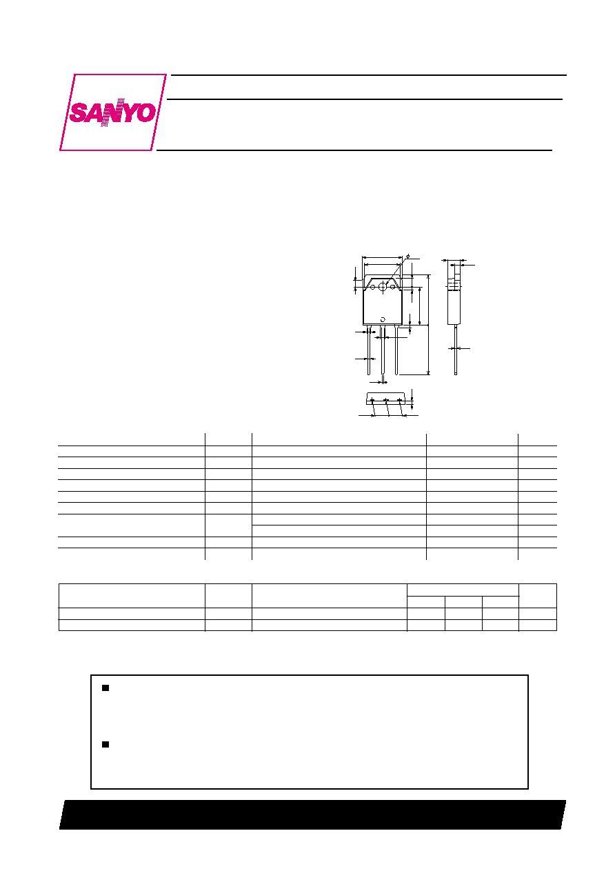
Package Dimensions
unit : mm
2022A
[2SC5960]
31504KB TS IM TA-100660
Any and all SANYO products described or contained herein do not have specifications that can handle
applications that require extremely high levels of reliability, such as life-support systems, aircraft's
control systems, or other applications whose failure can be reasonably expected to result in serious
physical and/or material damage. Consult with your SANYO representative nearest you before using
any SANYO products described or contained herein in such applications.
SANYO assumes no responsibility for equipment failures that result from using products at values that
exceed, even momentarily, rated values (such as maximum ratings, operating condition ranges, or other
parameters) listed in products specifications of any and all SANYO products described or contained
herein.
NPN Triple Diffused Planar Silicon Transistor
1 : Base
2 : Collector
3 : Emitter
SANYO : TO-3PB
15.6
2.6
3.5
1.2
14.0
1.6
1.0
2.0
0.6
20.0
20.0
15.0
1.3
3.2
4.8
2.0
0.6
5.45
5.45
1.4
1
2
3
SANYO Electric Co.,Ltd. Semiconductor Company
TOKYO OFFICE Tokyo Bldg., 1-10, 1 Chome, Ueno, Taito-ku, TOKYO, 110-8534 JAPAN
2SC5960
No.7610-2/4
6
10
8
4
2
0
0
2
6
4
8
1
3
7
5
9
10
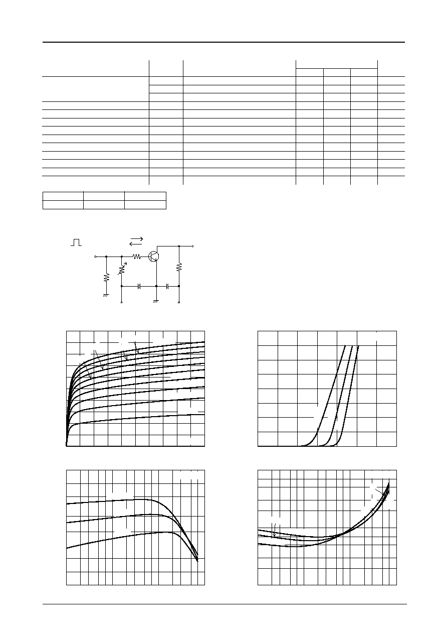
IC -- VCE
IT05057
1000mA
IB=0
300mA
200mA
100mA
400mA
500mA
600mA
5
9
7
3
1
700mA
800mA
900mA
Collector-to-Emitter Voltage, VCE -- V
Collector Current, I
C
--
A
Base-to-Emitter ON-State Voltage, VBE(on) -- V
Collector Current, I
C
--
A
IT05149
8
6
7
4
5
3
2
1
0
0
0.2
0.4
0.6
0.8
1.0
1.4
1.2
IC -- VBE(on)
VCE=5V
T
a=120
∞
C
25
∞
C
--40
∞
C
Collector Current, IC -- A
DC Current Gain, h
FE
10
7
5
100
7
5
3
2
2
3
5
7
2
3
5
7
2
3
5
7
0.1
0.01
1.0
10
hFE -- IC
IT05151
VCE=5V
Ta=120
∞
C
25
∞
C
--40
∞
C
Collector Current, IC -- A
Collector
-to-Emitter
Saturation V
oltage, V
CE
(sat) -
-
V
0.1
0.01
1.0
5
3
2
7
5
3
2
7
3
2
5 7
3
2
5 7
3
2
5 7
1.0
0.01
0.1
10
VCE(sat) -- IC
IT05152
IC / IB=5
Ta= --40
∞
C
Ta=120
∞
C
120
∞
C
--40
∞
C
25
∞
C
25
∞
C
Continued from preceding page.
Ratings
Parameter
Symbol
Conditions
min
typ
max
Unit
hFE1
VCE=5V, IC=0.8A
20*
50*
DC Current Gain
hFE2
VCE=5V, IC=4A
10
hFE3
VCE=5V, IC=1mA
10
Collector-to-Emitter Saturation Voltage
VCE(sat)
IC=4A, IB=0.8A
0.8
V
Base-to-Emitter Saturation Voltage
VBE(sat)
IC=4A, IB=0.8A
1.5
V
Gain-Bandwidth Product
fT
VCE=10V, IC=0.8A
15
MHz
Output Capacitance
Cob
VCB=10V, f=1MHz
50
pF
Collector-to-Base Breakdown Voltage
V(BR)CBO
IC=1mA, IE=0
500
V
Collector-to-Emitter Breakdown Voltage
V(BR)CEO
IC=5mA, RBE=
400
V
Emitter-to-Base Breakdown Voltage
V(BR)EBO
IE=1mA, IC=0
7
V
Turn-On Time
ton
IC=5A, IB1=1A, IB2=--2A, RL=40
, VCC=200V
0.5
µ
s
Storage Time
tstg
IC=5A, IB1=1A, IB2=--2A, RL=40
, VCC=200V
2.5
µ
s
Fall Time
tf
IC=5A, IB1=1A, IB2=--2A, RL=40
, VCC=200V
0.3
µ
s
* : The hFE1 of the 2SC5960 is classified as follows.
Rank
M
N
hFE
20 to 40
30 to 50
Switching Time Test Circuit
D.C.
1%
VR
RB
VCC=200V
VBE= --5V
+
+
50
INPUT
OUTPUT
RL
100
µ
F
470
µ
F
PW=20
µ
s
IB1
IB2
2SC5960
No.7610-3/4
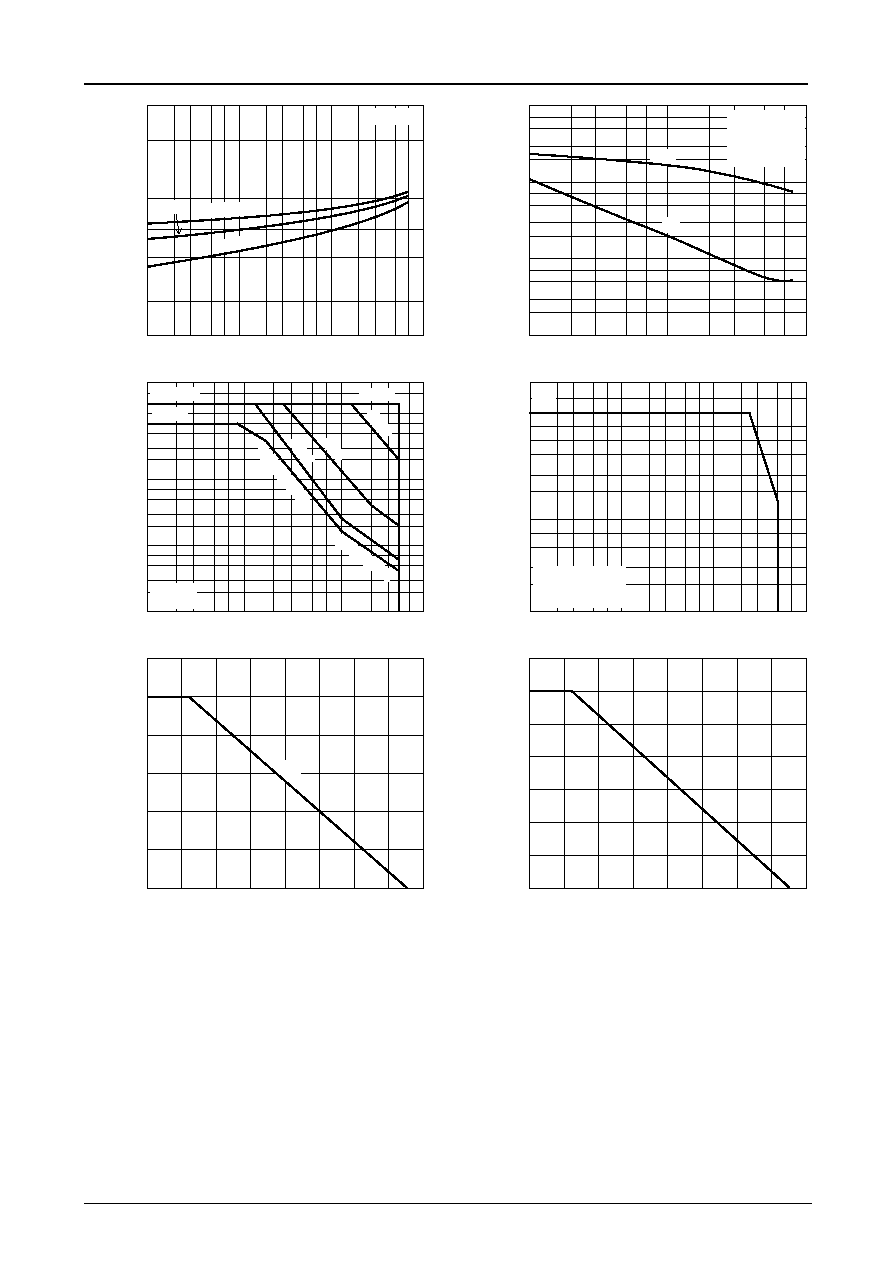
Reverse Bias A S O
IT05863
0.1
5
7
3
2
5
7
3
2
3
2
1.0
10
100
10
5
7
1.0
2
3
5
7
2
3
1000
5
7
2
3
IT05063
ICP
Tc=25
∞
C
IB2= --1.2A Const.
L=500
µ
H
Forward Bias A S O
Collector-to-Emitter Voltage, VCE -- V
Collector Current, I
C
-
-
A
Collector-to-Emitter Sustain Voltage, VCEX(sus) -- V
Collector Current, I
C
-
-
A
IT05864
Collector Current, IC -- A
SW Time -- IC
Switching
T
ime, SW
T
ime -
-
µ
s
0.1
0.01
5
7
3
2
5
7
3
2
5
7
3
2
1.0
10
1.0
0.1
2
3
5
7
2
3
5
7
10
IT05923
tstg
tf
VCC=200V
IC/IB=5
IB2/IB1= --2.5
R load
IT05150
7
1.0
5
3
2
3
2
0.01
7
5
3
2
0.1
7
5
3
2
1.0
7
5
3
2
10
VBE(sat) -- IC
IC / IB=5
Ta= --40
∞
C
120
∞
C
25
∞
C
Collector Current, IC -- A
Base-to-Emitter
Saturation V
oltage, V
BE
(sat) -
-
V
0.1
0.01
5
7
3
2
5
7
3
2
5
7
3
2
3
2
1.0
10
100
10
5
7
2
3
1.0
2
3
5
7
2
3
5
7
IT06395
10ms
1ms
DC operation
S / B Limited
100
µ
s
50
µ
s
ICP=14A
IC=7A
Tc=25
∞
C
Single pulse
0
0.5
1.0
1.5
2.0
3.0
2.5
0
PC -- Ta
40
20
100
120
60
80
140
160
Ambient Temperature, Ta --
∞
C
Collector Dissipation, P
C
-
-
W
No heat sink
0
10
20
30
40
50
60
70
0
PC -- Tc
40
20
100
120
60
80
140
160
Collector Dissipation, P
C
-
-
W
Case Temperature, Tc --
∞
C
2SC5960
No.7610-4/4
Specifications of any and all SANYO products described or contained herein stipulate the performance,
characteristics, and functions of the described products in the independent state, and are not guarantees
of the performance, characteristics, and functions of the described products as mounted in the customer's
products or equipment. To verify symptoms and states that cannot be evaluated in an independent device,
the customer should always evaluate and test devices mounted in the customer's products or equipment.
SANYO Electric Co., Ltd. strives to supply high-quality high-reliability products. However, any and all
semiconductor products fail with some probability. It is possible that these probabilistic failures could
give rise to accidents or events that could endanger human lives, that could give rise to smoke or fire,
or that could cause damage to other property. When designing equipment, adopt safety measures so
that these kinds of accidents or events cannot occur. Such measures include but are not limited to protective
circuits and error prevention circuits for safe design, redundant design, and structural design.
In the event that any or all SANYO products(including technical data,services) described or
contained herein are controlled under any of applicable local export control laws and regulations,
such products must not be expor ted without obtaining the expor t license from the author ities
concerned in accordance with the above law.
No part of this publication may be reproduced or transmitted in any form or by any means, electronic or
mechanical, including photocopying and recording, or any information storage or retrieval system,
or otherwise, without the prior written permission of SANYO Electric Co. , Ltd.
Any and all information described or contained herein are subject to change without notice due to
product/technology improvement, etc. When designing equipment, refer to the "Delivery Specification"
for the SANYO product that you intend to use.
Information (including circuit diagrams and circuit parameters) herein is for example only ; it is not
guaranteed for volume production. SANYO believes information herein is accurate and reliable, but
no guarantees are made or implied regarding its use or any infringements of intellectual property rights
or other rights of third parties.
This catalog provides information as of March, 2004. Specifications and information herein are subject
to change without notice.
PS