Specifications and information herein are subject to change without notice.
981224TM2fXHD
Absolute Maximum Ratings / Ta=25
∞
C
Drain to Source Voltage
Gate to Source Voltage
Drain Current (D.C)
Drain Current (Pulse)
Channel Temperature
Storage Temperature
Allowable power Dissipation
V
V
A
A
∞
C
∞
C
W
Electrical Characteristics / Ta=25
∞
C
Drain to Source Breakdown Voltage
Gate to Source Breakdown Voltage
Zero Gate Voltage Drain Current
Gate to Source Leakage Current
Cutoff Voltage
Static Drain to Source on State Resistance
Input Capacitance
Output Capacitance
Reverse Transfer Capacitance
Turn-ON Delay Time
Rise Time
Turn-oFF Delay Time
Fall Time
Diode Forward Voltage
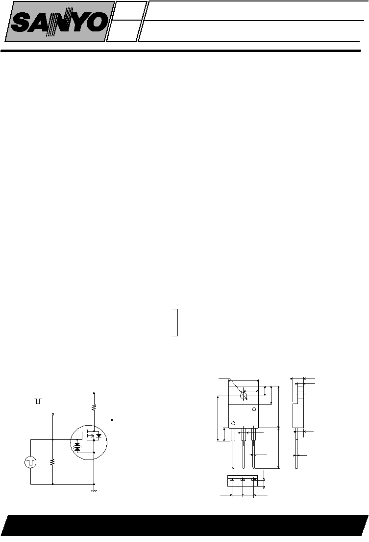
Switching Time Test Circuit
VDSS
VGSS
ID
IDP
PD
Tch
Tstg
TENTATIVE
PW
10
µ
S, dutycycle
1%
Tc=25
∞
C
unit
Forward Transfer Admittance
Features and Applications
∑ Low ON-state resistance.
∑ Very high-speed switching.
∑ Low-voltage dreve.
SANYO Electric Co., Ltd. Semiconductor Business Headquarters
TOKYO OFFICE Tokyo Bldg., 1-10,1 Chome, Ueno, taito-ku, 110 JAPAN
--60
±
20
--10
--40
150
--55 to +150
60
min
--60
±
20
--100
±
10
V
V
µ
A
µ
A
--1.0
V
S
pF
pF
pF
ns
ns
ns
ns
--2.0
4
0.15
7.5
0.11
0.15
1230
390
100
16
40
230
150
--1.0
V
0.2
--1.5
V(BR)DSS
V(BR)GSS
ID=--1mA , VGS=0
ID=
±
100
µ
A , VGS=0
IDSS
VDS=--60V , VGS=0
IGSS
VGS=
±
16V , VDS=0
VGS(OFF)
VDS=--10V , ID=--1mA
| yfs |
VDS=--10V , ID=--5A
RDS(On)1
ID=--5A , VGS=--10V
RDS(On)2
ID=--5A , VGS=--4V
Ciss
VDS=--20V , f=1MHz
Coss
VDS=--20V , f=1MHz
Crss
VDS=--20V , f=1MHz
td(On)
tr
td(Off)
tf
VSD
IS =--1.0A , VGS = 0
Case Outline
See Specified Test
Circuit .
2SJ261
P- Channel Silicon MOS FET
Very High-Speed Switching Applications
typ
max
unit
50
P.G
S
G
D
VOUT
VDD=--30V
VIN
ID=--5A
RL=--6
PW=10uS
D.C
1%
VIN
0V
--10V
2SJ261
TO-220(unit ; mm)
1 : Gate
2 : Drain
3 : Source
10.2
5.1
3.6
1.2
0.8
5.6
18.0
2.7
6.3
15.1
14.0
4.5
1.3
2.7
0.4
1
2
2.55
2.55
3
2.7