 | –≠–ª–µ–∫—Ç—Ä–æ–Ω–Ω—ã–π –∫–æ–º–ø–æ–Ω–µ–Ω—Ç: 2SK3738 | –°–∫–∞—á–∞—Ç—å:  PDF PDF  ZIP ZIP |
2SK3738
No.7671-1/3
Application
∑
Impedance conversion.
∑
Infrared sensor.
Features
∑
Small IGSS.
∑
Small Ciss.
∑
Ultrasmall package permitting applied sets to be
small and slim.
Specifications
Absolute Maximum Ratings
at Ta=25
∞
C
Parameter
Symbol
Conditions
Ratings
Unit
Drain-to-Source Voltage
VDSS
40
V
Gate-to-Drain Voltage
VGDS
--40
V
Gate Current
IG
10
mA
Drain Current
ID
1
mA
Allowable Power Dissipation
PD
100
mW
Junction Temperature
Tj
150
∞
C
Storage Temperature
Tstg
--55 to +150
∞
C
Electrical Characteristics
at Ta=25
∞
C
Ratings
Parameter
Symbol
Conditions
min
typ
max
Unit
Gate-to-Drain Breakdown Voltage
V(BR)GDS
IG=--10
µ
A, VDS=0
--40
V
Gate-to-Source Leakage Current
IGSS
VGS=--20V, VDS=0
--500
pA
Cutoff Voltage
VGS(off)
VDS=10V, ID=1
µ
A
--1.5
--2.3
V
Zero-Gate Voltage Drain Current
IDSS
VDS=10V, VGS=0
50
130
µ
A
Forward Transfer Admittance
yfs
VDS=10V, VGS=0, f=1kHz
0.06
0.13
mS
Input Capacitance
Ciss
VDS=10V, VGS=0, f=1MHz
1.7
pF
Reverse Transfer Capacitance
Crss
VDS=10V, VGS=0, f=1MHz
0.7
pF
Marking : KB
N-Channel Junction Silicon FET
Ordering number : ENN7671
2SK3738
42004GB TS IM TA-100829
Any and all SANYO products described or contained herein do not have specifications that can handle
applications that require extremely high levels of reliability, such as life-support systems, aircraft's
control systems, or other applications whose failure can be reasonably expected to result in serious
physical and/or material damage. Consult with your SANYO representative nearest you before using
any SANYO products described or contained herein in such applications.
SANYO assumes no responsibility for equipment failures that result from using products at values that
exceed, even momentarily, rated values (such as maximum ratings, operating condition ranges, or other
parameters) listed in products specifications of any and all SANYO products described or contained
herein.
Impedance Converter Applications
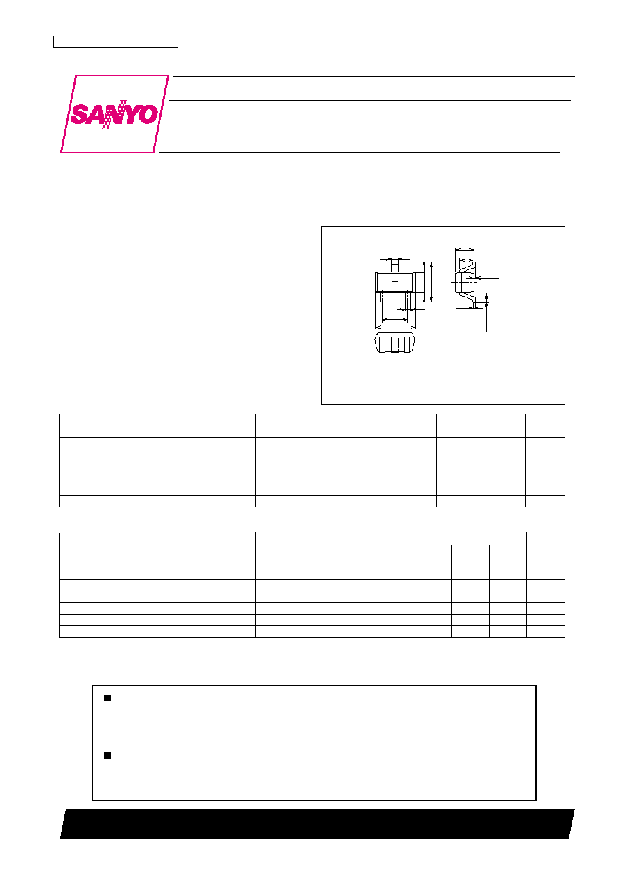
Package Dimensions
unit : mm
2124
[2SK3738]
SANYO Electric Co.,Ltd. Semiconductor Company
TOKYO OFFICE Tokyo Bldg., 1-10, 1 Chome, Ueno, Taito-ku, TOKYO, 110-8534 JAPAN
1 : Source
2 : Drain
3 : Gate
SANYO : SMCP
0.8
0.4
0.4
2
3
1.6
0.2
1.6
0.3
0.5
1
0.5
0.75
0.6
0~0.1
0.1
0.1max
2SK3738
No.7671-2/3
ITR00837
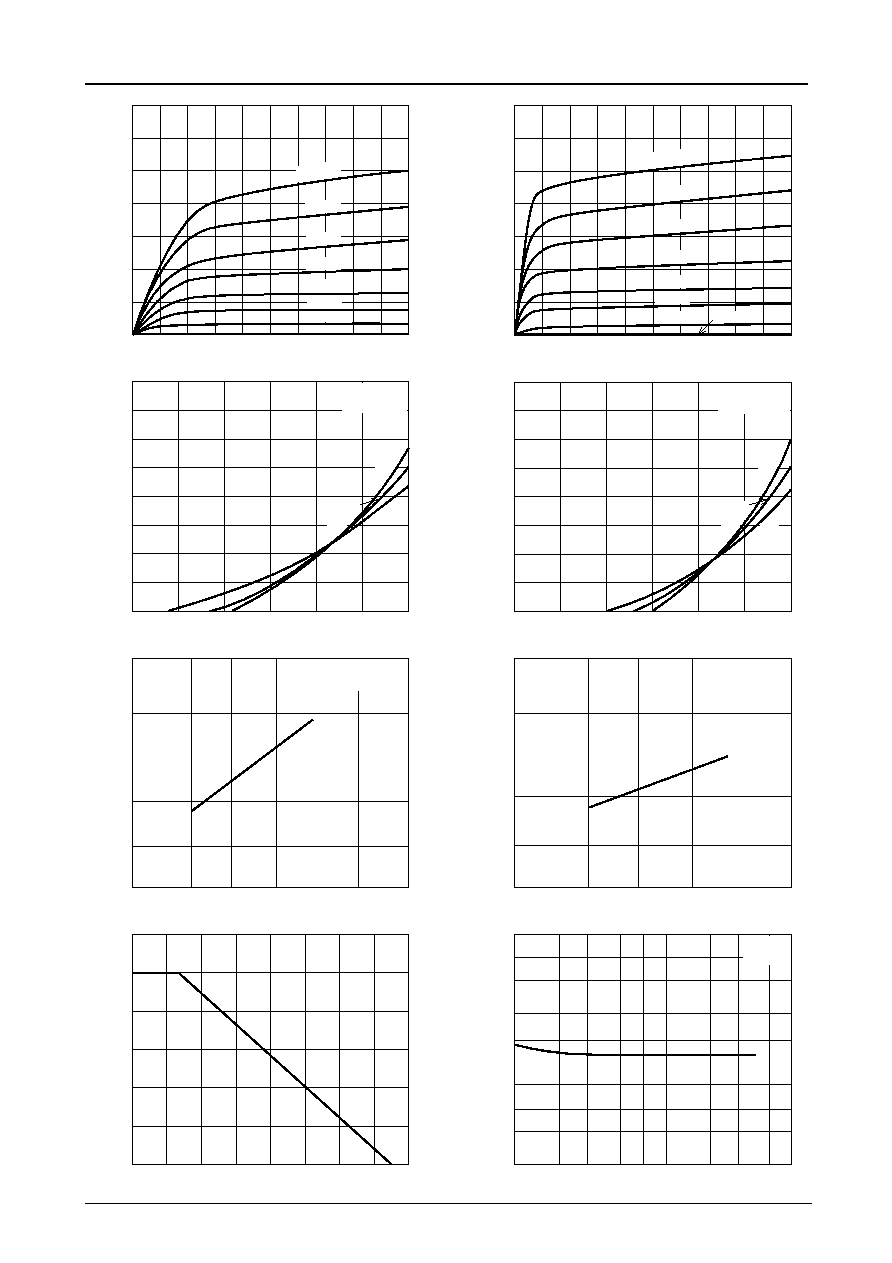
ID -- VDS
0
1
2
3
4
5
0
20
40
60
80
140
100
120
VGS=0
--0.2V
--0.4V
--0.6V
--0.8V
--1.0V
--1.2V
--1.4V
VGS=0
--0.2V
--0.4V
--0.6V
--0.8V
--1.0V
--1.2V
--1.4V
ITR00839
ID -- VGS
--1.2
--1.0
--0.8
--0.6
--0.4
--0.2
0
0
10
20
30
40
50
60
70
80
ITR00838
ID -- VDS
0
4
8
12
16
20
0
20
40
60
80
100
120
140
VGS(off) -- IDSS
IT06669
y
fs
-- IDSS
IT06668
VDS=10V
IDSS=50
µ
A
VDS=10V
IDSS=100
µ
A
ITR00840
ID -- VGS
--2.0
--2.4
--1.6
--1.2
--0.8
--0.4
0
0
20
40
60
80
100
120
140
160
0
20
40
60
80
100
120
160
140
0
20
40
80
100
60
120
PD -- Ta
IT06670
Ta=25
∞
C
75
∞
C
--25
∞
C
Ta=25
∞
C
75
∞
C
--25
∞
C
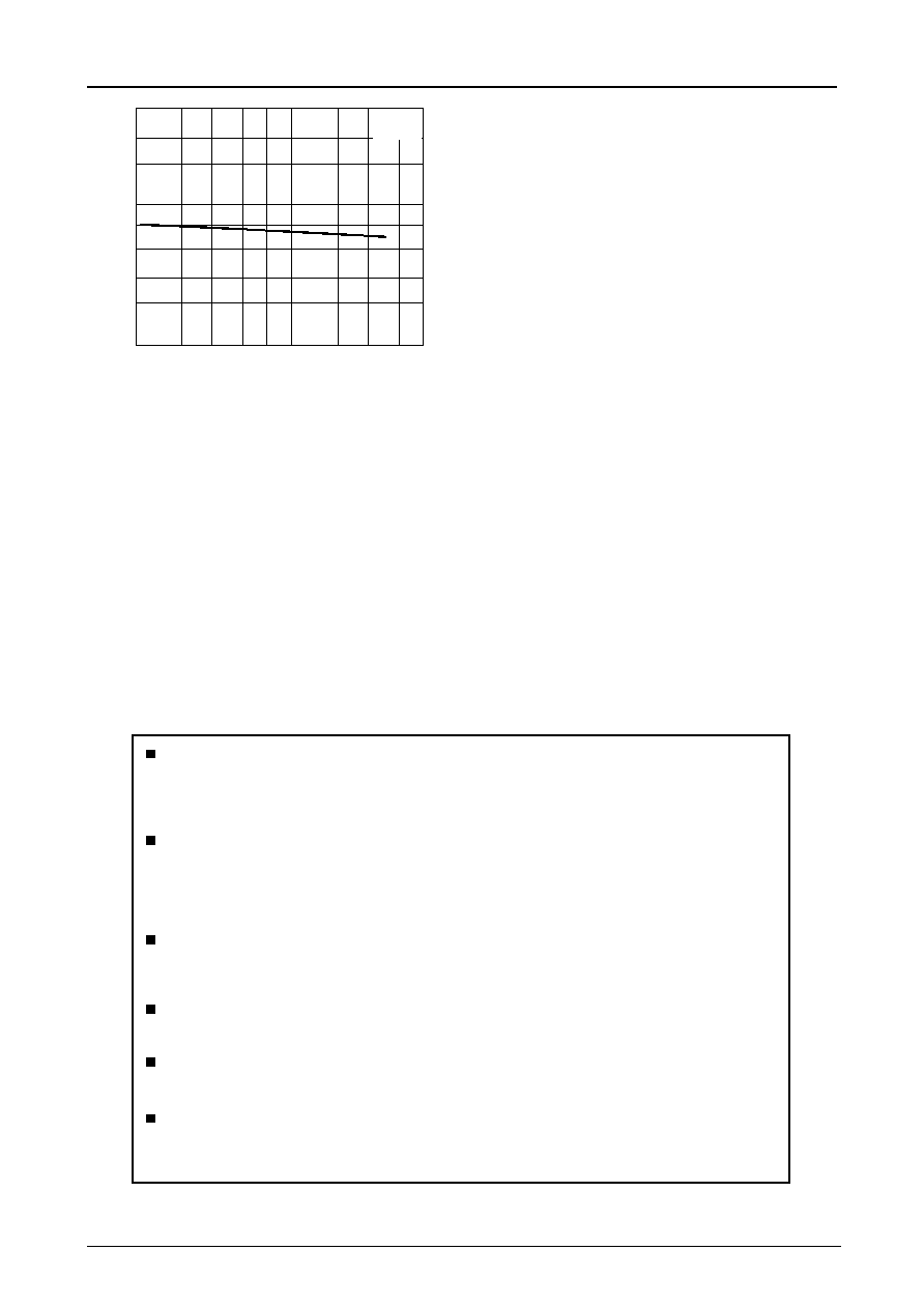
IT06671
VGS=0
f=1MHz
1.0
2
3
5
7
10
3
5
7
2
2
7
5
7
5
3
3
1.0
10
Ciss -- VDS
Drain-to-Source Voltage, VDS -- V
Input Capacitance, Ciss -
-
pF
Ambient Temperature, Ta --
∞
C
Allo
w
able Po
wer Dissipation, P
D
-
-
mW
Drain Current, IDSS --
µ
A
F
orw
ard T
ransfer
Admittance,
y
fs
-
-
mS
Drain Current, IDSS --
µ
A
Cutof
f
V
oltage, V
GS
(of
f)
--
V
Gate-to-Source Voltage, VGS -- V
Gate-to-Source Voltage, VGS -- V
Drain Current, I
D
--
µ
A
Drain Current, I
D
--
µ
A
Drain Current, I
D
--
µ
A
Drain Current, I
D
--
µ
A
Drain-to-Source Voltage, VDS -- V
Drain-to-Source Voltage, VDS -- V
5
7
2
3
3
100
7
--1.0
3
5
2
VDS=10V
ID=1
µ
A
2
3
7
5
100
3
2
0.1
5
7
VDS=10V
VGS=0
f=1kHz
2SK3738
No.7671-3/3
Specifications of any and all SANYO products described or contained herein stipulate the performance,
characteristics, and functions of the described products in the independent state, and are not guarantees
of the performance, characteristics, and functions of the described products as mounted in the customer's
products or equipment. To verify symptoms and states that cannot be evaluated in an independent device,
the customer should always evaluate and test devices mounted in the customer's products or equipment.
SANYO Electric Co., Ltd. strives to supply high-quality high-reliability products. However, any and all
semiconductor products fail with some probability. It is possible that these probabilistic failures could
give rise to accidents or events that could endanger human lives, that could give rise to smoke or fire,
or that could cause damage to other property. When designing equipment, adopt safety measures so
that these kinds of accidents or events cannot occur. Such measures include but are not limited to protective
circuits and error prevention circuits for safe design, redundant design, and structural design.
In the event that any or all SANYO products(including technical data,services) described or
contained herein are controlled under any of applicable local export control laws and regulations,
such products must not be exported without obtaining the export license from the authorities
concerned in accordance with the above law.
No part of this publication may be reproduced or transmitted in any form or by any means, electronic or
mechanical, including photocopying and recording, or any information storage or retrieval system,
or otherwise, without the prior written permission of SANYO Electric Co. , Ltd.
Any and all information described or contained herein are subject to change without notice due to
product/technology improvement, etc. When designing equipment, refer to the "Delivery Specification"
for the SANYO product that you intend to use.
Information (including circuit diagrams and circuit parameters) herein is for example only ; it is not
guaranteed for volume production. SANYO believes information herein is accurate and reliable, but
no guarantees are made or implied regarding its use or any infringements of intellectual property rights
or other rights of third parties.
This catalog provides information as of April, 2004. Specifications and information herein are subject
to change without notice.
PS
IT06672
VGS=0
f=1MHz
1.0
2
3
5
7
10
5
7
2
3
1.0
0.1
2
7
5
3
2
5
3
Crss -- VDS
Drain-to-Source Voltage, VDS -- V
Re
v
erse
T
ransfer Capacitance, Crss -
-
pF