13001 RM (IM) No.6764-1/8
Ver.1.6
12898
Overview
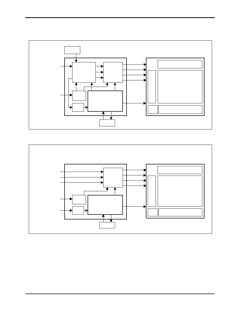
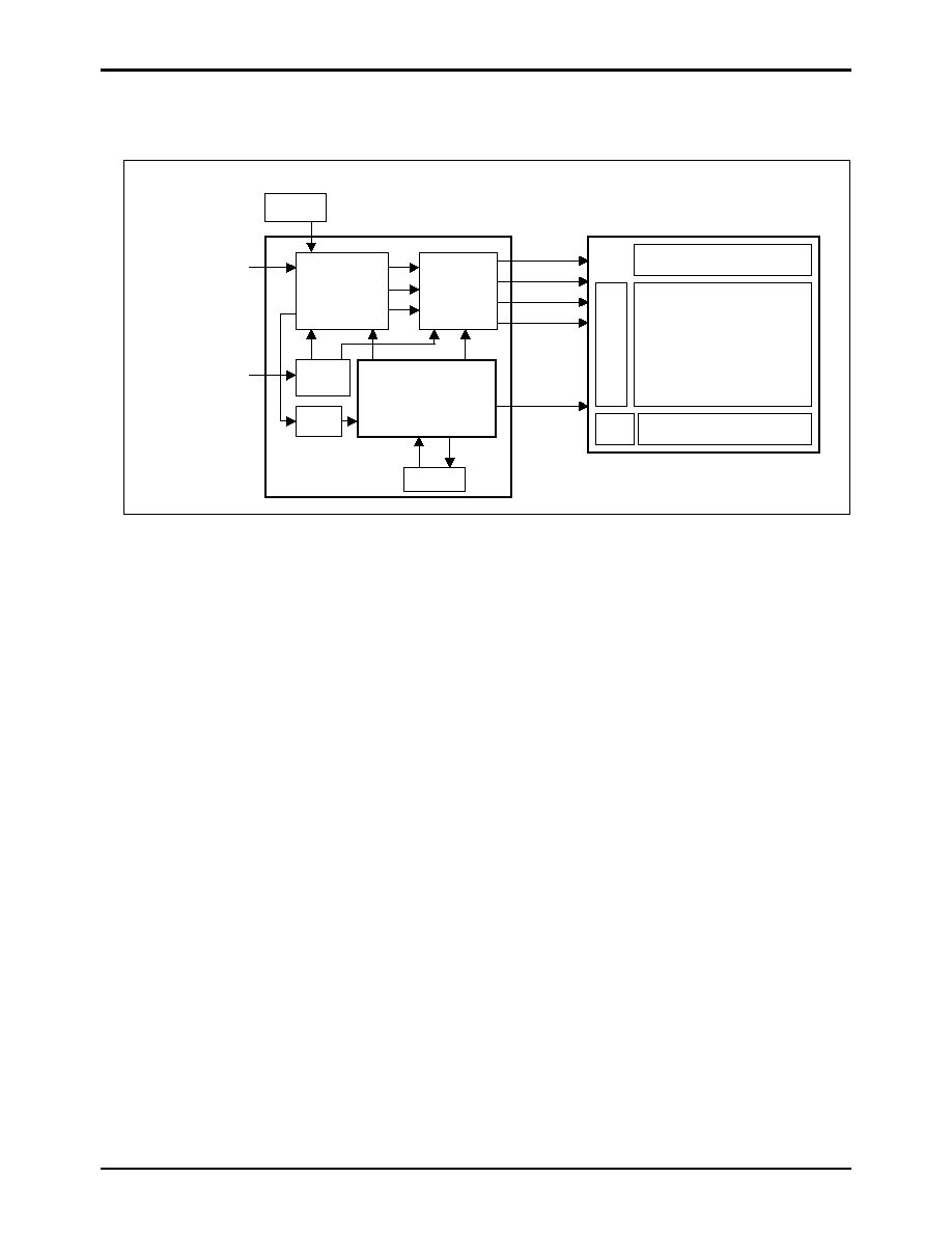
This wide viewing type 2.5 inch low temperature poly- silicon TFT-LCD module consists of LCD panel and backlight.
This is suitable for digital still camera or for digital video camera.
Features
∑ Diagonal 6.3cm (2.5inch) display size.
∑ 881 ◊ 228 = 200,868 dots.
∑ RGB delta color arrangement.
∑ Wide viewing angle,
Survival
Æ
. (Super Ranged Viewing by Vertical Alignment)
∑ Operating temperature (Panel) is -10 to +60∞C. Ambient temperature during storage is -20 to +70∞C.
∑ Slim design, light weight and narrow frame. (t=0.7mm glass)
∑ Up / down and right / left inverse function.
∑ Built-in shifter circuit.
∑ Conform to NTSC, PAL when using recommended IC : LV4131W, LV4133W, (LV4139W : Under development).
∑ Wide-viewing film, Anti-glare (AG) / Anti-reflection (AR) coat.
∑ Builds in fluorescent lamp backlight unit. (Not contains inverter unit)
∑ Panel power consumption is Typ.171mW at NTSC.
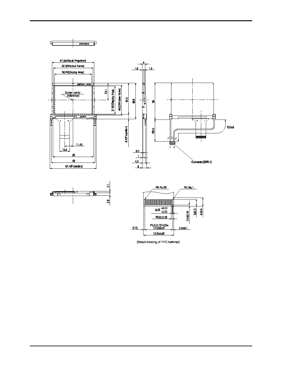
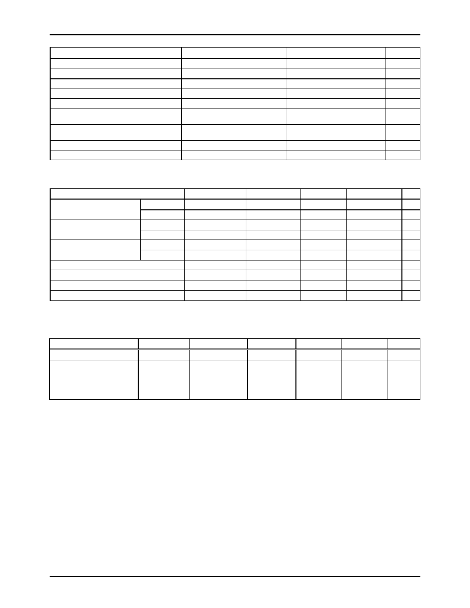
Specifications
Item Specifications
Unit
Remarks
Dot count (H) ◊ (V)
881 ◊ 228
dot
Effective display dimensions (H) ◊ (V)
50.25 ◊ 37.62
mm
Display size (diagonal)
6.3(2.5inch)
cm
Dot pitch (H) ◊ (V)
0.057 ◊ 0.165
mm
Color arrangement
RGB Delta
-
External Dimensions (W) ◊ (H) ◊ (D)
TYP 62.4 ◊ 48.6 ◊ 6.0
mm
Note1
Weight TBD
g
*Note1: Excluding flexible cable and protrusions.
Low-Temperature Polysilicon
2.5-inch TFT LCD Module
ALP234FCX
Ordering number : ENN6764
LCD Module
ALP234FCX
No.6764-2/8
Absolute Maximum Ratings
at HVSS=0V, VVSS=0V
Item Symbol
Ratings
Unit
H driver power supply voltage
HVDD
-1.0 to +17
V
V driver power supply voltage
VVDD
-1.0 to +17
V
Common electrode voltage
VCOM
-1.0 to +17
V
Driving direction signal voltage
CSH, CSV
-1.0 to +17
V
H driver input voltage
STH, XSTH, CKH1, CKH2
-1.0 to +17
V
V driver / precharge data
input voltage
STV, XSTV, CKV1, CKV2,
ENB, XENB, PCG, XPCG
-1.0 to +17
V
Video / precharge data
input voltage
VG, VR, VB, VPCD
-1.0 to +13
V
Operating temperature (panel)
Topr
-10 to +60
∞
C
Storage temperature
Tstg
-20 to +70
∞
C
Operating Conditions
Power supply voltage
HVDD 15.5V ± 0.5V, VVDD 15.5V ± 0.5V, VVSS 0V, HVSS 0V
Item Symbol
MIN
TYP
MAX
Unit
Low VHIL -0.3 0.0 0.3
V
H driver input voltage
High VHIH 2.5 3.0 4.0
V
Low VVIL -0.3 0.0 0.3
V
V driver input voltage
High VVIH 2.5 3.0 4.0
V
Low VSIL -0.3 0.0 0.3
V
CSV, CSH
High VSIH 11.5 VDD VDD
V
Video signal center voltage
VVC
6.3
6.5
6.8
V
Video signal input voltage range *1
VG, VR, VB
VVC-5.0
-
VVC+5.0
V
Common electrode voltage*2
VCOM
(VVC-3.5)-0.2
(VVC-3.5)
(VVC-3.5)+0.2
V
Precharge data signal *1
VPCD
-
VVC±5.0
-
V
*1 Video signal and precharge data signal shall be input symmetrically around VVC.
*2 Set common electrode voltage to the optimum voltage.
Optical Specifications
Item Symbol
Condition
MIN
TYP
MAX
Unit
Contrast ratio
CR
25
∞
C
- 100 -
-
T 50
B 50
L 50
Viewing angle range
R
CR >= 10
-
50
- deg
ALP234FCX
No.6764-3/8
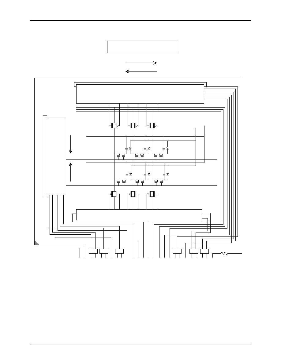
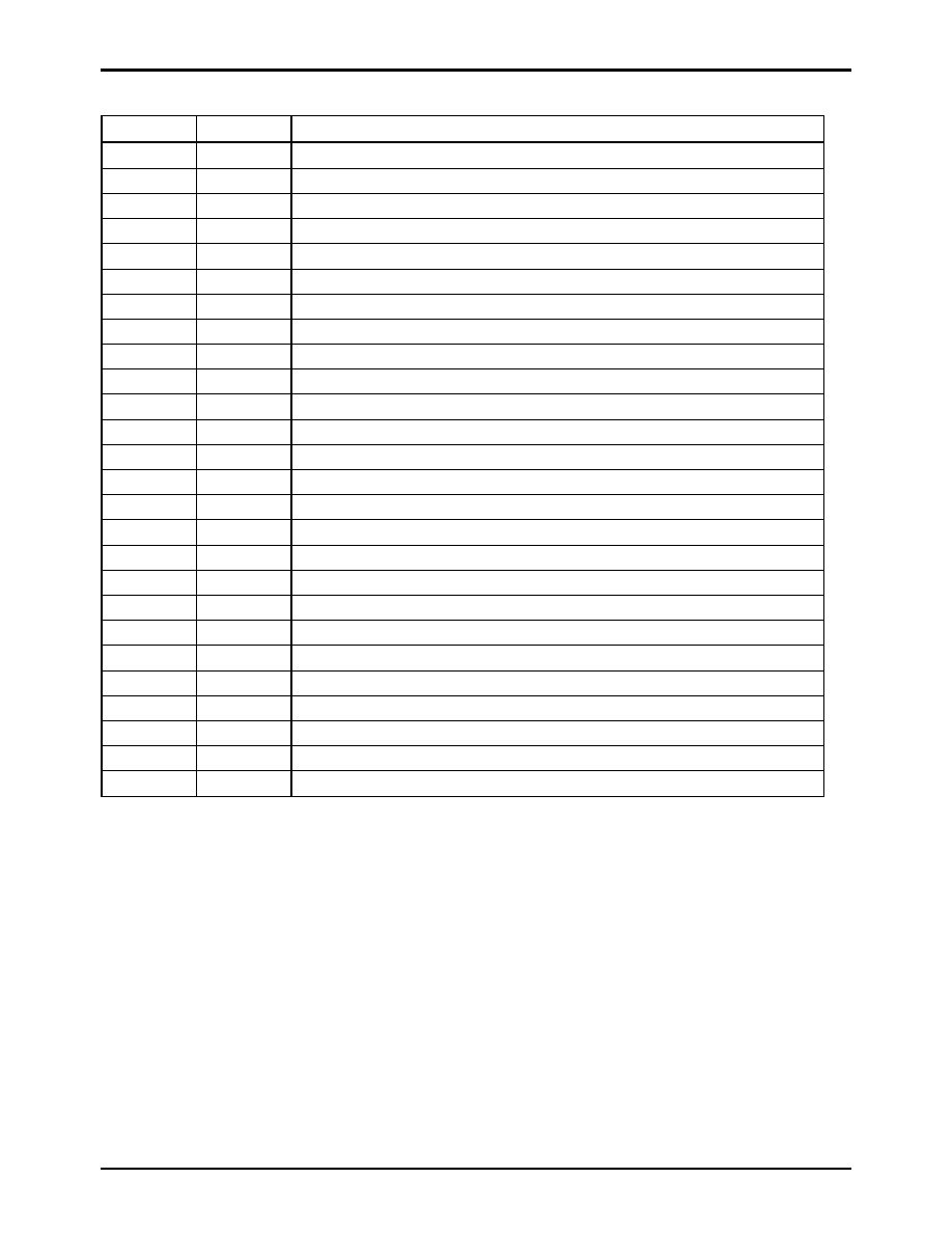
Pin Function
Pin No
Symbol
Function
1
NC
Leave this pin open
2
COM
Common electrode voltage
3
CKV2
V clock 2
4
CKV1
V clock 1
5
XSTV
Inverted signal of STV
6
STV
V start signal
7
VVSS
VSS for V drive
8
XENB
Inverted signal of ENB
9 ENB
Enable
signal
10
VVDD
VDD for V drive
11
CSV
Up / down inverse control signal (H : Normal scan, L : Reverse scan)
12
NC
Leave this pin open
13
PCD
Precharge data signal
14
B
Video signal (B)
15
R
Video signal (R)
16
G
Video signal (G)
17
CSH
Right / left inverse control signal (H : Normal scan, L : Reverse scan)
18
HVSS
VSS for H drive
19
XSTH
Inverted signal of STH
20
STH
H start signal
21
HVDD
VDD for H drive
22
XPCG
Inverted signal of PCG
23
PCG
Precharge gate signal
24
CKH2
H clock 2
25
CKH1
H clock 1
26
NC
Leave this pin open