 | –≠–ª–µ–∫—Ç—Ä–æ–Ω–Ω—ã–π –∫–æ–º–ø–æ–Ω–µ–Ω—Ç: ALP239CXX | –°–∫–∞—á–∞—Ç—å:  PDF PDF  ZIP ZIP |
13001 RM (IM) No.6772-1/8
Ver.1.6
12898
Overview
This 2 inch low temperature poly- silicon TFT-LCD module is suitable for digital still camera or for digital video camera.
Features
∑ Diagonal 5.1cm (2.0inch) display size.
∑ 557 ◊ 234 = 130,338 dots.
∑ RGB delta color arrangement.
∑ Operating temperature (panel) is -10 to +60∞C. Ambient temperature during storage is -20 to +70∞C.
∑ Slim design, light weight and narrow frame. (t=0.7mm glass)
∑ Up / down and right / left inverse function.
∑ Built-in level shifter circuit.
∑ Conform to NTSC, PAL when using recommended IC : LV4135W, LV4137W, (LV4139W : Under development)
∑ Anti-reflection (AR) coat.
∑ Panel power consumption is Typ.61mW at NTSC.
∑ Optical transmittance is approx. 8%.
∑ Low power consumption by 12V drive.
Specifications
Item Specifications
Unit
Remarks
Dot count (H) ◊ (V)
557 ◊ 234
dot
Effective display dimensions (H) ◊ (V)
40.98 ◊ 30.77
mm
Display size (diagonal)
5.1 (2.0inch)
cm
Dot pitch (H) ◊ (V)
0.0735 ◊ 0.1315
mm
Color arrangement
RGB Delta
-
External Dimensions (W) ◊ (H) ◊ (D)
TYP 47.9 ◊ 39.9 ◊ 2.1
mm
Note1
Weight Approx.
8
g
*Note1: Excluding flexible cable and protrusions.
Low-Temperature Polysilicon
2.0-inch TFT LCD Module
ALP239CXX
Ordering number : ENN6772
LCD Module
ALP239CXX
No.6772-2/8
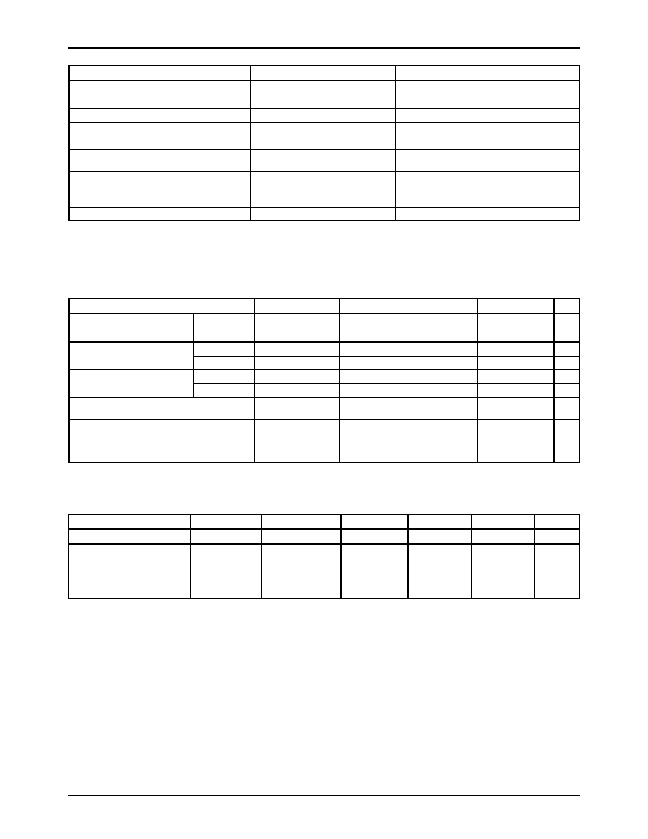
Absolute Maximum Ratings
at VSS=0V
Item Symbol
Ratings
Unit
H driver power supply voltage
HVDD
-1.0 to +14
V
V driver power supply voltage
VVDD
-1.0 to +14
V
Common electrode voltage
VCOM
-1.0 to +14
V
Driving direction signal voltage
CSH, CSV
-1.0 to +14
V
H driver input voltage
STH, XSTH, CKH1, CKH2
-1.0 to +14
V
V driver / precharge data
input voltage
STV, XSTV, CKV1, CKV2,
ENB, XENB, PCG, XPCG
-1.0 to +14
V
Video / precharge data
input voltage
VG, VR, VB, VPCD
-1.0 to +13
V
Operating temperature (panel)
Topr
-10 to +60
∞
C
Storage temperature
Tstg
-20 to +70
∞
C
Operating Conditions
Power supply voltage
HVDD LV4135W LV4137W : 12.0V±0.3V
VVDD LV4135W LV4137W : 12.0V±0.3V
VSS LV4135W LV4137W : 0V
Item Symbol
MIN
TYP
MAX
Unit
Low VHIL -0.3 0.0 0.3
V
H driver input voltage
High VHIH 2.5 3.0 4.0
V
Low VVIL -0.3 0.0 0.3
V
V driver input voltage
High VVIH 2.5 3.0 4.0
V
Low VSIL -0.3 0.0 0.3
V
CSV, CSH
High VSIH 11.5 VDD VDD
V
Video signal
center voltage
LV4135W, LV4137W
VVC
5.0
5.2
5.4
V
Video signal input voltage range *1
VG, VR, VB
VVC-3.5
-
VVC+3.5
V
Common electrode voltage*2
VCOM
(VVC-0.2)-0.2
(VVC-0.2)
(VVC-0.2)+0.2
V
Precharge data signal *1
VPCD
VVC±1.5
VVC±2.0
VVC±2.5
V
*1 Video signal and precharge data signal shall be input symmetrically around VVC.
*2 Set common electrode voltage to the optimum voltage.
Optical Specifications
Item Symbol
Condition
MIN
TYP
MAX
Unit
Contrast ratio
CR
25
∞
C
- 100 -
-
T 15
B 35
L 45
Viewing angle range
R
CR >= 10
-
45
- deg

ALP239CXX
No.6772-3/8
Pin Function
Pin No
Symbol
Function
1
NC
Leave this pin open
2
COM
Common electrode voltage
3
CKV1
V clock 1
4
CKV2
V clock 2
5
VVDD
VDD for V drive
6
STV
V start signal
7
XSTV
Inverted signal of STV
8
CSV
Up / down inverse control signal (H : Normal scan, L : Reverse scan)
9 ENB
Enable
signal
10
XENB
Inverted signal of ENB
11
PCD
Precharge data signal
12
B
Video signal (B)
13
R
Video signal (R)
14
G
Video signal (G)
15
VSS
VSS for V and H drive
16
XPCG
Inverted signal of PCG
17
PCG
Precharge gate signal
18
CSH
Right / left inverse control signal (H : Normal scan, L : Reverse scan)
19
XSTH
Inverted signal of STH
20
STH
H start signal
21
CKH2
H clock 2
22
CKH1
H clock 1
23
HVDD
VDD for H drive
24
NC
Leave this pin open
ALP239CXX
No.6772-4/8
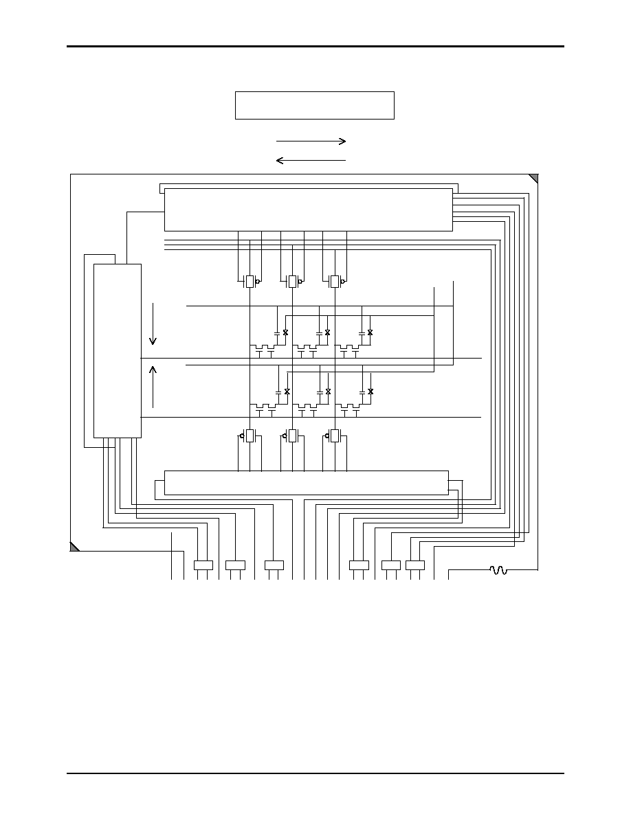
Block Diagram
H-DRIVER
G
R
B
PRECHARGE CIRCUIT
VVDD
COM
...
...
...
...
...
...
...
...
24
.
N
C
23
.
H
V
D
D
22
.
C
K
H
1
21
.
C
K
H
2
20
.
S
TH
19
.
X
S
T
H
18
.
C
S
H
17
.
P
C
G
16
.
X
P
C
G
1
5
.
VSS
14
.
G
13
.
R
12
.
B
11
.
P
C
D
10
.
X
E
N
B
9.
E
N
B
8.
C
S
V
7.
X
S
T
V
6.
S
T
V
5
.
VVDD
4
.
CKV2
3
.
CKV1
2.
C
O
M
1.
N
C
STH
CKH1
CKH2
HVDD
CSH
VSS
VSS
V
-
DRI
VE
R
L/S
PCD
VVD
D
EN
B
CS
V
ST
V
C
KV2
C
KV1
PCG
XPCG
VSS
L/S
L/S
L/S
L/S
L/S
Front View
Normal Scan
Reverse Scan
Reverse Scan
Normal Scan
ALP239CXX
No.6772-5/8
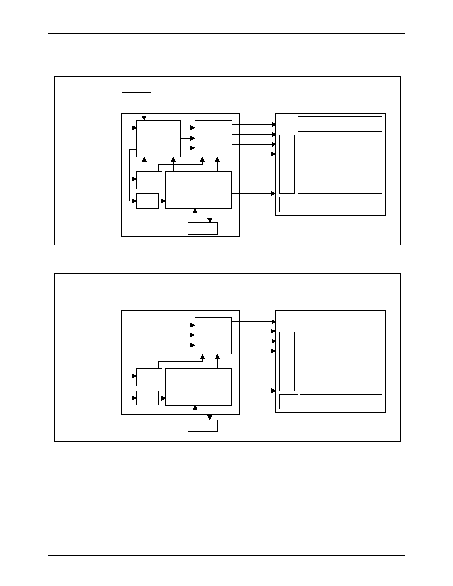
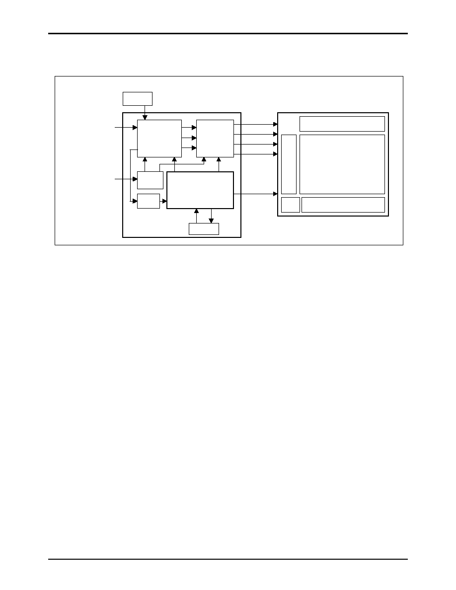
System Configuration
ALP 239
Video
chrom a
signal
processing
RG B
drivers
(S&H)
Tim ing
controller
VCO
X'tal
LV 4137W
S ig nal processing IC
R
G
B
R
G
Horizontal scanner
Display area
Precharge circuit
V
e
r
t
i
c
al
sc
ann
er
Lo w -tem perature p-S i
TF T-L C D
BUS
I/F
Serial control
Sync.
sep.
PCD
Level
shifter
B
Video signal
Com posite
Y/C
Y/Color
difference
RG B
drivers
(S&H)
Tim ing
controller
VCO
Analog RG B
LV 4135W
S ig nal processing IC
R
G
B
R
G
Horizontal scanner
Display area
Precharge circuit
V
e
r
t
i
c
al
sc
ann
er
Lo w -tem perature p-S i
TF T-L C D
BUS
I/F
Serial control
Sync.
sep.
PCD
Level
shifter
Synchronus
signal
Video signal
ALP 239
B
ALP239CXX
No.6772-6/8
System Configuration
Video
chrom a
signal
processing
RG B
drivers
(S&H)
Tim ing
controller
VCO
X'tal
Video signal
Com posite
Y/C
Y/Color
difference
R
G
B
R
G
Horizontal scanner
Display area
Precharge circuit
V
e
r
t
i
c
al
sc
ann
er
Lo w -tem perature p-S i
TF T-L C D
BUS
I/F
Serial control
Sync.
sep.
PCD
Level
shifter
ALP 239
B
LV 4139W
S ig nal processing IC
**Un der develo pm ent
ALP239CXX
No.6772-7/8
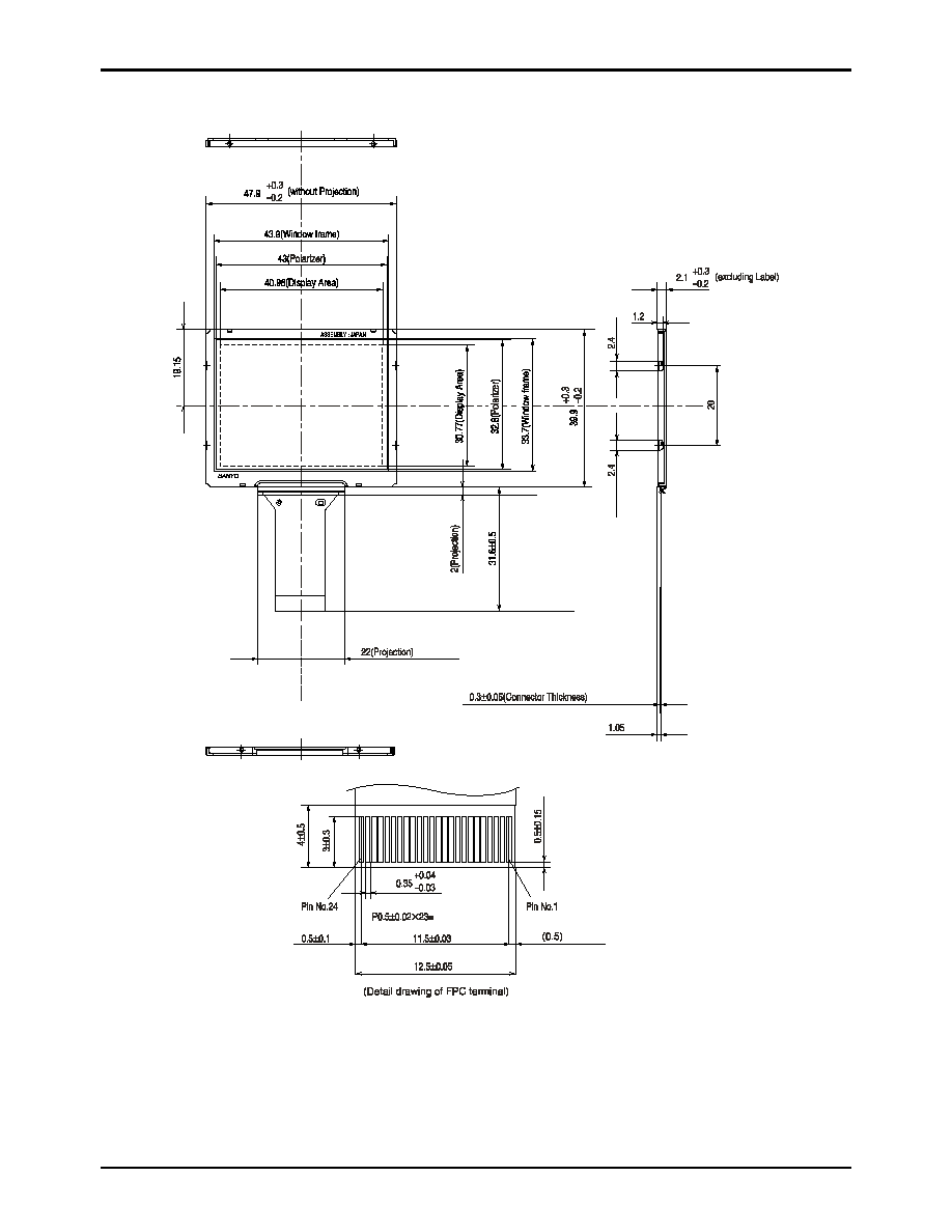
Package Dimension
ALP239CXX
No.6772-8/8
PS