 | –≠–ª–µ–∫—Ç—Ä–æ–Ω–Ω—ã–π –∫–æ–º–ø–æ–Ω–µ–Ω—Ç: CPH5811 | –°–∫–∞—á–∞—Ç—å:  PDF PDF  ZIP ZIP |
CPH5811
No.8234-1/6
SANYO Electric Co.,Ltd. Semiconductor Company
TOKYO OFFICE Tokyo Bldg., 1-10, 1 Chome, Ueno, Taito-ku, TOKYO, 110-8534 JAPAN
Ordering number : ENN8234
CPH5811
MOSFET : N-Channel Silicon MOSFET
SBD : Schottky Barrier Diode
DC / DC Converter Applications
Features
∑
Composite type with an N-Channel Sillicon MOSFET (MCH3406) and a Schottky Barrier Diode (SBS004)
contained in one package facilitating high-density mounting.
[MOSFET]
∑
Low ON-resistance.
∑
Ultrahigh-speed switching.
∑
1.8V driver
[SBD]
∑
Short reverse recovery time.
∑
Low forward voltage.
Specifications
Absolute Maximum Ratings
at Ta=25
∞
C
Parameter
Symbol
Conditions
Ratings
Unit
[MOSFET]
Drain-to-Source Voltage
VDSS
20
V
Gate-to-Source Voltage
VGSS
±
10
V
Drain Current (DC)
ID
3
A
Drain Current (Pulse)
IDP
PW
10
µ
s, duty cycle
1%
12
A
Allowable Power Dissipation
PD
Mounted on a ceramic board (600mm
2
!
0.8mm) 1unit
0.9
W
Channel Temperature
Tch
150
∞
C
Storage Temperature
Tstg
--55 to +125
∞
C
[SBD]
Repetitive Peak Reverse Voltage
VRRM
15
V
Nonrepetitive Peak Reverse Surge Voltage
VRSM
15
V
Average Output Current
IO
1
A
Surge Forward Current
IFSM
50Hz sine wave, 1 cycle
10
A
Junction Temperature
Tj
--55 to +125
∞
C
Storage Temperature
Tstg
--55 to +125
∞
C
Marking : QM
Any and all SANYO products described or contained herein do not have specifications that can handle
applications that require extremely high levels of reliability, such as life-support systems, aircraft's
control systems, or other applications whose failure can be reasonably expected to result in serious
physical and/or material damage. Consult with your SANYO representative nearest you before using
any SANYO products described or contained herein in such applications.
SANYO assumes no responsibility for equipment failures that result from using products at values that
exceed, even momentarily, rated values (such as maximum ratings, operating condition ranges, or other
parameters) listed in products specifications of any and all SANYO products described or contained
herein.
22805PE TS IM TB-00001212
CPH5811
No.8234-2/6
Electrical Characteristics
at Ta=25
∞
C
Ratings
Parameter
Symbol
Conditions
min
typ
max
Unit
[MOSFET]
Drain-to-Source Breakdown Voltage
V(BR)DSS
ID=1mA, VGS=0
20
V
Zero-Gate Voltage Drain Current
IDSS
VDS=20V, VGS=0
1
µ
A
Gate-to-Source Leakage Current
IGSS
VGS=
±
8V, VDS=0
±
10
µ
A
Cutoff Voltage
VGS(off)
VDS=10V, ID=1mA
0.4
1.3
V
Forward Transfer Admittance
yfs
VDS=10V, ID=1.5A
3.36
5.6
S
RDS(on)1
ID=1.5A, VGS=4V
48
63
m
Static Drain-to-Source On-State Resistance
RDS(on)2
ID=1A, VGS=2.5V
58
82
m
RDS(on)3
ID=0.5A, VGS=1.8V
72
100
m
Input Capacitance
Ciss
VDS=10V, f=1MHz
280
pF
Output Capacitance
Coss
VDS=10V, f=1MHz
60
pF
Reverse Transfer Capacitance
Crss
VDS=10V, f=1MHz
38
pF
Turn-ON Delay Time
td(on)
See specified Test Circuit.
13
ns
Rise Time
tr
See specified Test Circuit.
35
ns
Turn-OFF Delay Time
td(off)
See specified Test Circuit.
35
ns
Fall Time
tf
See specified Test Circuit.
25
ns
Total Gate Charge
Qg
VDS=10V, VGS=4V, ID=3A
8.8
nC
Gate-to-Source Charge
Qgs
VDS=10V, VGS=4V, ID=3A
0.85
nC
Gate-to-Drain "Miller" Charge
Qgd
VDS=10V, VGS=4V, ID=3A
0.85
nC
Diode Forward Voltage
VSD
IS=3A, VGS=0
0.82
1.2
V
[SBD]
Reverse Voltage
VR
IR=1mA
15
V
Forward Voltage
VF1
IF=0.5A
0.30
0.35
V
VF2
IF=1A
0.35
0.40
V
Reverse Current
IR
VR=6V
500
µ
A
Interterminal Capacitance
C
VR=10V, f=1MHz cycle
42
pF
Reverse Recovery Time
trr
IF=IR=100mA, See specified Test Circuit.
15
ns
Therminal Resistance
Rth(j-a)
Mounted on a ceramic board (600mm
2
!
0.8mm)
110
∞
C / W
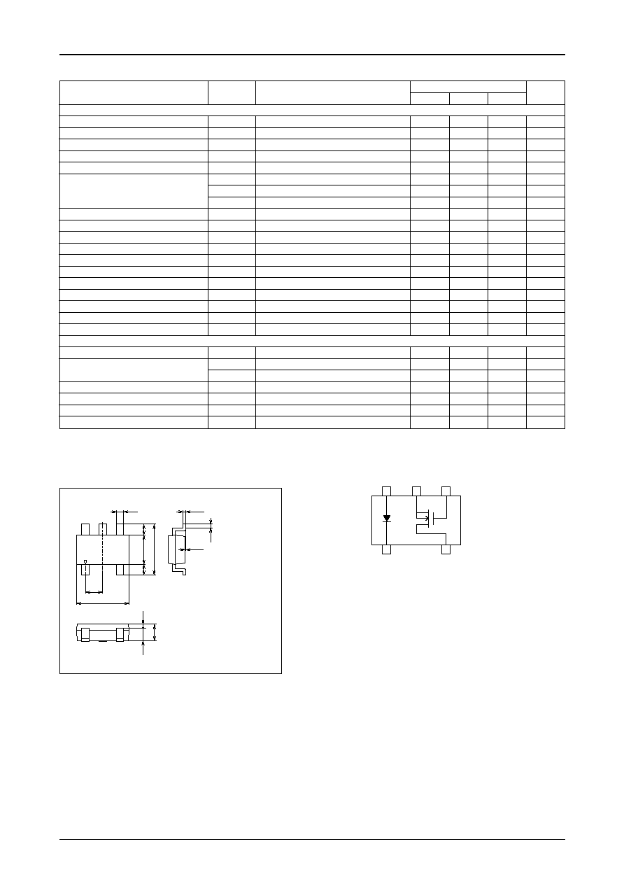
Package Dimensions
Electrical Connection
unit : mm
2171A
1 : Cathode
2 : Drain
3 : Gate
4 : Source
5 : Anode
SANYO : CPH5
2.9
0.95
0.05
1
2
3
4
5
0.2
0.7
0.9
2.8
1.6
0.6
0.6
0.2
0.4
0.15
1
4
2
5
3
1 : Cathode
2 : Drain
3 : Gate
4 : Source
5 : Anode
Top view
CPH5811
No.8234-3/6
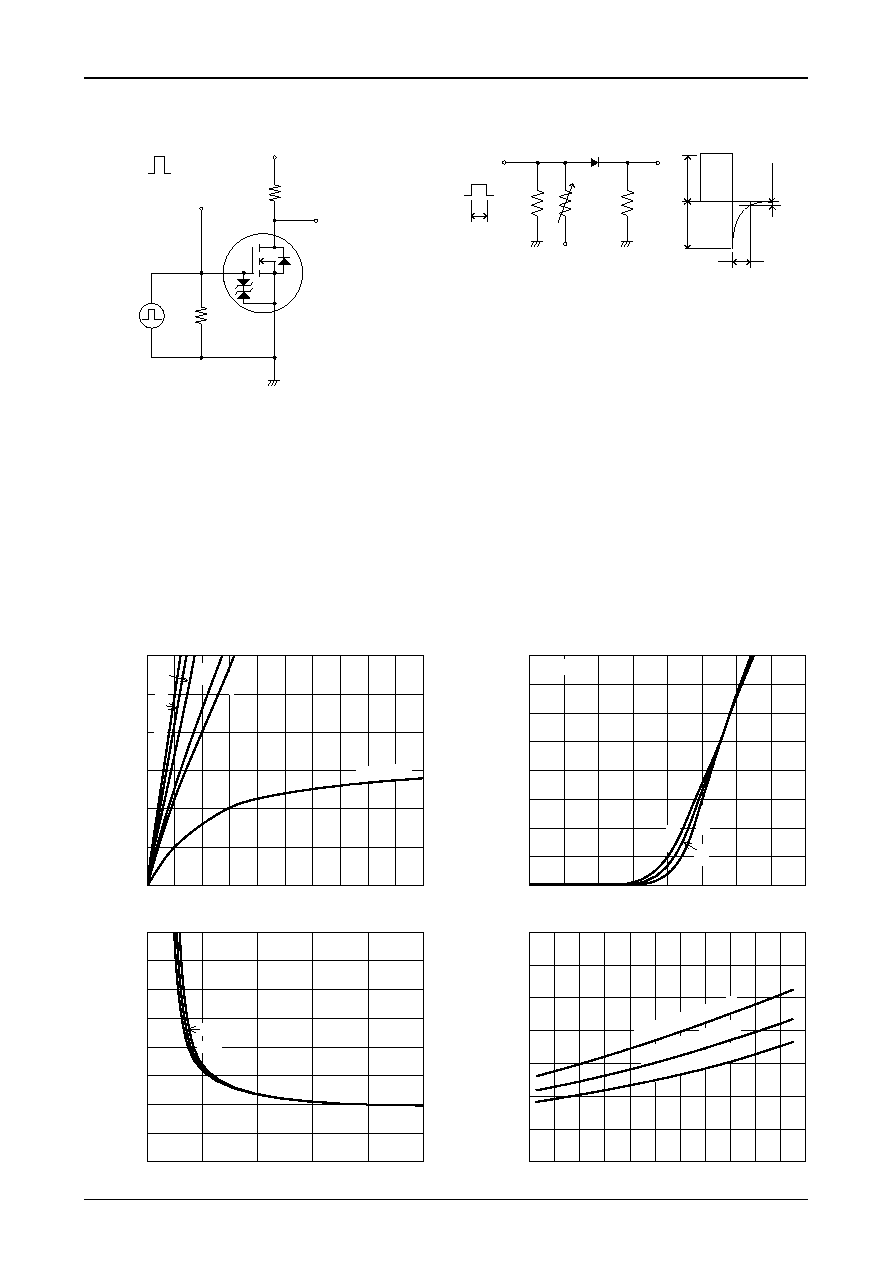
Switching Time Test Circuit
trr Test Circuit
[MOSFET]
[SBD]
PW=10
µ
s
D.C.
1%
P.G
50
G
S
D
ID=1.5A
RL=6.67
VDD=10V
VOUT
CPH5811
VIN
4V
0V
VIN
Duty
10%
50
100
10
--5V
trr
100mA
100mA
10mA
10
µ
s
20
40
60
80
100
120
140
0
20
40
60
80
100
120
140
160
0
0
0.5
1.0
1.5
2.0
2.5
3.0
3.5
4.0
--60
--40
--20
0
20
40
60
80
100
120
140
160
IT03492
0.5
1.0
1.5
2.0
2.5
3.0
0
0
0.1
0.2
0.3
0.4
0.5
0.6
0.7
0.8
0.9
1.0
IT03490
IT03491
IT03493
ID=0.5A, V
GS
=1.8V
ID=1.0A, V
GS
=2.5V
ID=1.5A, V
GS
=4.0V
VGS=1.0V
10.0V
--25
∞
C
T
a=75
∞
C
0
2
4
6
8
10
ID=0.5A
1.5A
Ta=25
∞
C
4.0V
2.5V
1.8V
1.5V
0
0.2
0.4
0.6
0.8
1.0
1.2
1.4
1.6
VDS=10V
25
∞
C
1.0A
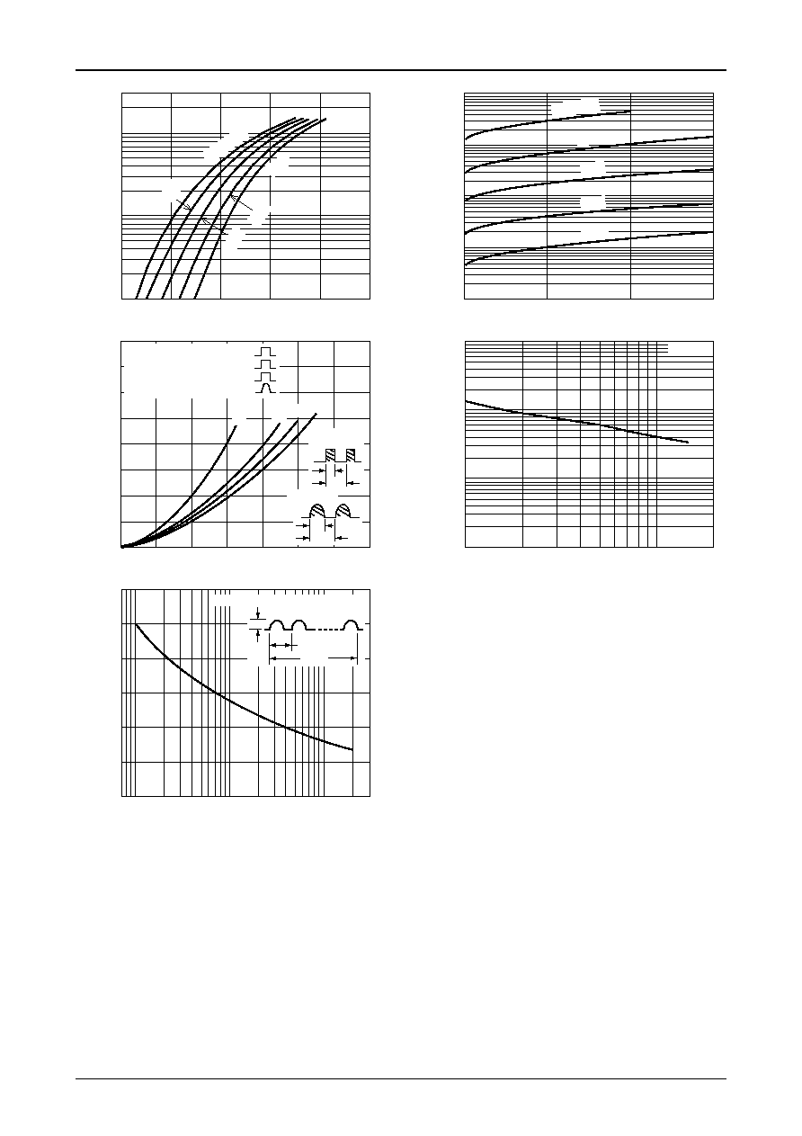
RDS(on) -- VGS
ID -- VDS
ID -- VGS
RDS(on) -- Ta
Static Drain-to-Source
On-State Resistance, R
DS
(on) -
-
m
Static Drain-to-Source
On-State Resistance, R
DS
(on) -
-
m
Gate-to-Source Voltage, VGS -- V
Drain-to-Source Voltage, VDS -- V
Drain Current, I
D
--
A
Gate-to-Source Voltage, VGS -- V
Drain Current, I
D
--
A
Ambient Temperature, Ta --
∞
C
[MOSFET]
[MOSFET]
[MOSFET]
[MOSFET]
CPH5811
No.8234-4/6
0
1
2
3
4
5
6
7
8
9
10
0.1
2
3
5
7
1.0
2
3
5
7
10
1.0
10
100
7
5
3
2
3
2
7
5
3
2
IT03498
0.5
1.0
1.5
2.0
2.5
3.0
3.5
4.0
0
VDD=10V
VGS=4V
td(on)
td(off)
t r
IT03496
IT03494
0.1
2
3
5
7 1.0
0.01
2
3
5
7
2
3
5
7 10
0.1
1.0
10
7
5
3
2
3
2
7
5
3
2
VDS=10V
75
∞
C
Ta= -
-25
∞
C
IT03495
0.2
0.3
0.4
0.5
0.6
0.7
0.8
0.9
1.0
1.1
1.2
0
2
4
6
8
10
12
14
16
18
20
0.1
1.0
7
5
3
2
10
7
5
3
2
0.01
7
5
3
2
VGS=0
--25
∞
C
25
∞
C
T
a=75
∞
C
IT03497
10
100
2
7
5
3
1000
2
7
5
3
Ciss
Coss
Crss
f=1MHz
VDS=10V
ID=3A
25
∞
C
tf
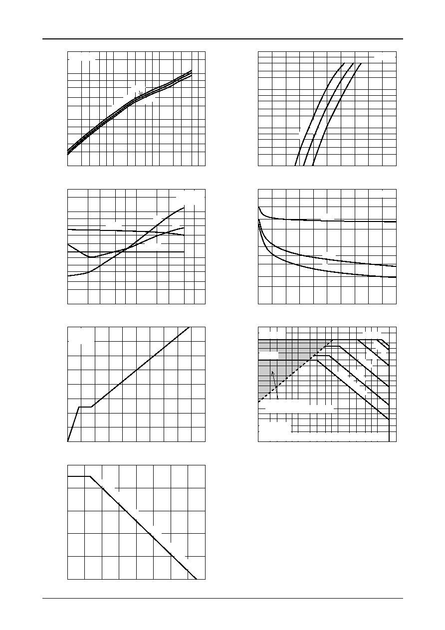
SW Time -- ID
Ciss, Coss, Crss -- VDS
y
fs
-- ID
IF -- VSD
Drain Current, ID -- A
Switching
T
ime, SW
T
ime -
-
ns
Drain Current, ID -- A
Forward T
ransfer
Admittance,
y
fs
-
-
S
Diode Forward Voltage, VSD -- V
Forward Current, I
F
--
A
Drain-to-Source Voltage, VDS -- V
Ciss, Coss, Crss -
-
pF
VGS -- Qg
PD -- Ta
A S O
Total Gate Charge, Qg -- nC
Gate-to-Source V
oltage, V
GS
--
V
Ambient Temperature, Ta --
∞
C
Allowable Power Dissipation, P
D
--
W
Drain-to-Source Voltage, VDS -- V
Drain Current, I
D
-
-
A
[MOSFET]
[MOSFET]
[MOSFET]
[MOSFET]
[MOSFET]
[MOSFET]
[MOSFET]
0.2
0.4
0.6
0.8
0.9
1.0
0
0
20
40
60
80
100
120
140
160
IT09178
0.01
2
2
3
5
7
10
1.0
2
3
5
7
0.1
3
5
7
2
3
2
3
5 7
1.0
10
2
3
5 7
0.1
2
3
5 7
0.01
2
3
IT09177
IDP=12A
ID=3A
Operation in this
area is limited by RDS(on).
100
µ
s
100ms
DC operation
1ms
10ms
<10
µ
s
Ta=25
∞
C
Single pulse
Mounted on a ceramic board (600mm
2
!0.8mm) 1unit
Mounted on a ceramic board (600mm
2
!
0.8mm) 1unit
CPH5811
No.8234-5/6
1.0
10
2
2
3
5
100
1000
1.0
10
7
2
3
5
7
2
3
5
7
3
5
7
2
Reverse Voltage, VR -- V
C -- VR
Interterminal Capacitance, C
-
-
pF
f=1MHz
0
100
10
1.0
0.1
0.01
5
7
3
2
5
7
3
2
5
7
3
2
5
7
3
2
15
5
10
Reverse Voltage, VR -- V
IR -- VR
Reverse Current, I
R
-
-
mA
0
0
0.2
0.4
0.6
0.8
0.8
0.7
0.6
0.4
0.3
0.2
0.1
0.5
1.0
1.2
1.4
Average Forward Current, IO -- A
PF(AV) -- IO
A
verage Forward Power Dissipation, P
F
(A
V)
-
-
W
0
0.1
0.01
0.3
0.4
0.5
0.1
0.2
1.0
3
2
7
5
3
2
7
5
3
2
Forward Voltage, VF -- V
Forward Current, I
F
--
A
IF -- VF
Ta=125
∞
C
25
∞
C
50
∞
C
75
∞
C
100
∞
C
Ta=125
∞
C
25
∞
C
50
∞
C
75
∞
C
100
∞
C
IT00622
IT00623
IT00624
IT00625
[SBD]
[SBD]
[SBD]
[SBD]
(1)
(2) (4)
(3)
7 0.01
2
3
7 0.1
0
5
2
2
3
7 1.0
5
12
10
8
6
4
2
3
Time, t -- s
Sur
ge Forward Current, I
FSM
(Peak)
--
A
IT00626
[SBD]
Is
20ms
t
Current waveform 50Hz sine wave
IFSM -- t
180
∞
360
∞
360
∞
(1)Rectangular wav
e
=60
∞
(2)Rectangular wav
e
=120
∞
(3)Rectangular wav
e
=180
∞
(4)Sine wav
e
=180
∞
Sine
wave
Rectangular
wave

CPH5811
No.8234-6/6
Specifications of any and all SANYO products described or contained herein stipulate the performance,
characteristics, and functions of the described products in the independent state, and are not guarantees
of the performance, characteristics, and functions of the described products as mounted in the customer's
products or equipment. To verify symptoms and states that cannot be evaluated in an independent device,
the customer should always evaluate and test devices mounted in the customer's products or equipment.
SANYO Electric Co., Ltd. strives to supply high-quality high-reliability products. However, any and all
semiconductor products fail with some probability. It is possible that these probabilistic failures could
give rise to accidents or events that could endanger human lives, that could give rise to smoke or fire,
or that could cause damage to other property. When designing equipment, adopt safety measures so
that these kinds of accidents or events cannot occur. Such measures include but are not limited to protective
circuits and error prevention circuits for safe design, redundant design, and structural design.
In the event that any or all SANYO products(including technical data,services) described or
contained herein are controlled under any of applicable local export control laws and regulations,
such products must not be exported without obtaining the export license from the authorities
concerned in accordance with the above law.
No part of this publication may be reproduced or transmitted in any form or by any means, electronic or
mechanical, including photocopying and recording, or any information storage or retrieval system,
or otherwise, without the prior written permission of SANYO Electric Co. , Ltd.
Any and all information described or contained herein are subject to change without notice due to
product/technology improvement, etc. When designing equipment, refer to the "Delivery Specification"
for the SANYO product that you intend to use.
Information (including circuit diagrams and circuit parameters) herein is for example only ; it is not
guaranteed for volume production. SANYO believes information herein is accurate and reliable, but
no guarantees are made or implied regarding its use or any infringements of intellectual property rights
or other rights of third parties.
This catalog provides information as of February, 2005. Specifications and information herein are subject
to change without notice.
PS
Note on usage : Since the CPH5811 is a MOSFET product, please avoid using this device in the vicinity
of highly charged objects.