DBA20
No.647-1/2
Features
∑
Plastic molded structure.
∑
Glass passivation for high reliability.
∑
Peak reverse voltage : VRM=200, 600V.
∑
Average rectified current : IO=2.0A.
Specifications
Absolute Maximum Ratings
at Ta=25
∞
C
Parameter
Symbol
Conditions
DBA20C
DBA20G
Unit
Peak Reverse Voltage
VRM
200
600
V
Average Recitified Current
IO
Ta=40
∞
C
®
2.0
A
Surge Forward Current
IFSM
50Hz sine wave, 1cycle
®
40
A
Junction Temperature
Tj
®
150
∞
C
Storage Temperature
Tstg
®
--30 to +150
∞
C
Electrical Characteristics
at Ta=25
∞
C
Ratings
Parameter
Symbol
Conditions
min
typ
max
Unit
Forward Voltage
VF
IF=1.0A
1.05
V
Reverse Current
IR
VR : At each VRM
10
µ
A
Note : Mountiong torque : 0.49N∑m max.
SANYO Electric Co.,Ltd. Semiconductor Company
TOKYO OFFICE Tokyo Bldg., 1-10, 1 Chome, Ueno, Taito-ku, TOKYO, 110-8534 JAPAN
Ordering number : ENN647D
DBA20
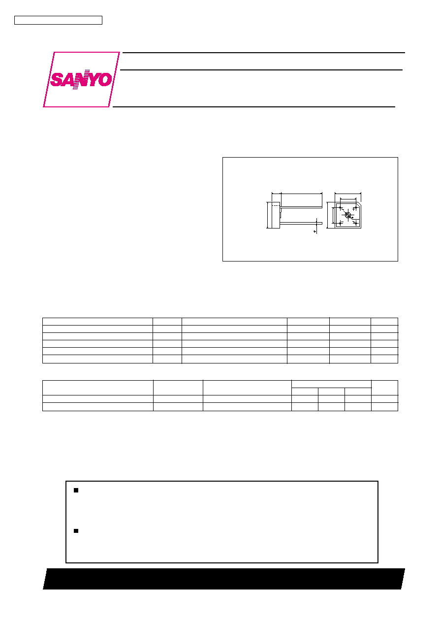
Package Dimensions
unit : mm
1087
[DBA20]
41000 GI IM / 52098 HA (KT) / 1129 YT, TS
Any and all SANYO products described or contained herein do not have specifications that can handle
applications that require extremely high levels of reliability, such as life-support systems, aircraft's
control systems, or other applications whose failure can be reasonably expected to result in serious
physical and/or material damage. Consult with your SANYO representative nearest you before using
any SANYO products described or contained herein in such applications.
SANYO assumes no responsibility for equipment failures that result from using products at values that
exceed, even momentarily, rated values (such as maximum ratings, operating condition ranges, or other
parameters) listed in products specifications of any and all SANYO products described or contained
herein.
Diffused Junction Type Silicon Diode
2.0A Single-Phase Bridge Rectifier
12.5
20.0 min
7.0
7.5
12.5
12.5
7.5
3.2
1.2
DBA20
No.647-2/2
Specifications of any and all SANYO products described or contained herein stipulate the performance,
characteristics, and functions of the described products in the independent state, and are not guarantees
of the performance, characteristics, and functions of the described products as mounted in the customer's
products or equipment. To verify symptoms and states that cannot be evaluated in an independent device,
the customer should always evaluate and test devices mounted in the customer's products or equipment.
SANYO Electric Co., Ltd. strives to supply high-quality high-reliability products. However, any and all
semiconductor products fail with some probability. It is possible that these probabilistic failures could
give rise to accidents or events that could endanger human lives, that could give rise to smoke or fire,
or that could cause damage to other property. When designing equipment, adopt safety measures so
that these kinds of accidents or events cannot occur. Such measures include but are not limited to protective
circuits and error prevention circuits for safe design, redundant design, and structural design.
In the event that any or all SANYO products(including technical data,services) described or
contained herein are controlled under any of applicable local export control laws and regulations,
such products must not be exported without obtaining the export license from the authorities
concerned in accordance with the above law.
No part of this publication may be reproduced or transmitted in any form or by any means, electronic or
mechanical, including photocopying and recording, or any information storage or retrieval system,
or otherwise, without the prior written permission of SANYO Electric Co. , Ltd.
Any and all information described or contained herein are subject to change without notice due to
product/technology improvement, etc. When designing equipment, refer to the "Delivery Specification"
for the SANYO product that you intend to use.
Information (including circuit diagrams and circuit parameters) herein is for example only ; it is not
guaranteed for volume production. SANYO believes information herein is accurate and reliable, but
no guarantees are made or implied regarding its use or any infringements of intellectual property rights
or other rights of third parties.
This catalog provides information as of April, 2000. Specifications and information herein are subject to
change without notice.
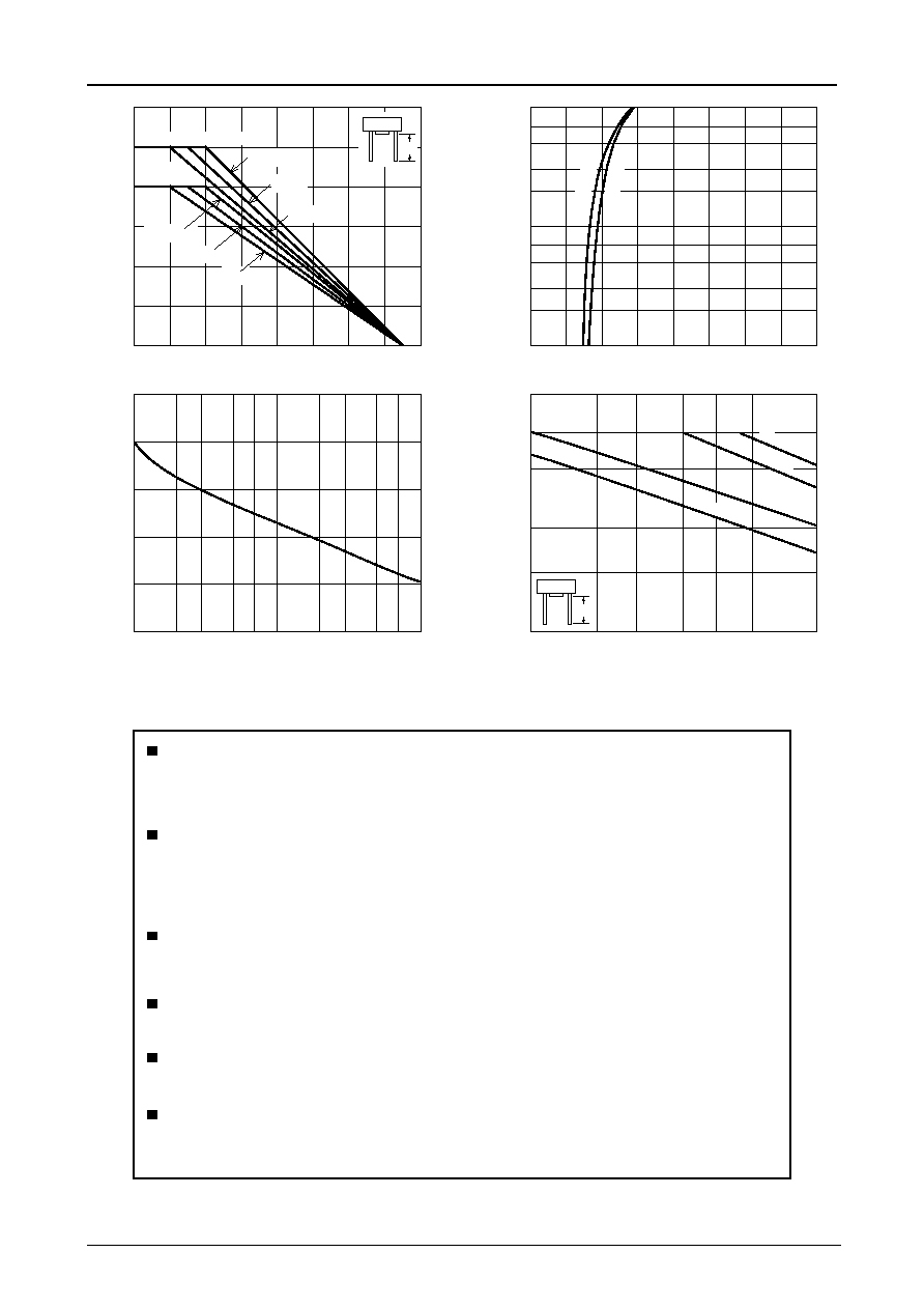
PS
Sur
ge F
o
w
ard Current, I
FSM
--
A
Number of Cycles at 50Hz, n
IFSM -- n
Solder Dip Time, t -- s
Soldering Temperature -- t
Solder
T
emperature -
-
∞
C
0
20
40
60
80
100
120
140
160
0
0.4
0.8
1.2
1.6
2.4
2.0
0
0.5
1.0
1.5
2.0
2.5
3.0
3.5
4.0
0
10
20
30
40
50
Ambient Temperature, Ta --
∞
C
IO -- Ta
A
v
erage Rectif
ied Current, I
O
--
A
0.1
1.0
10
5
7
2
3
5
7
2
3
100
5
3
4
2
Forward Voltage, VF -- V
IF -- VF
F
orw
ard Current, I
F
--
A
ID01172
ID01174
ID01173
ID01171
1.0
10
2
5
3
7
100
2
5
3
7
1.0
10
2
5
3
7
2
Resistive, inductive load
Capacitive
load
10mm
1.5mm
5mm
L=15mm
50Hz
T
a=150
∞
C
25
∞
C
L
L
L=20mm
5mm
15mm
5mm
L=20mm
15mm