
81004TN (OT) No. 7944-1/24
Any and all SANYO products described or contained herein do not have specifications that can handle
applications that require extremely high levels of reliability, such as life-support systems, aircraft's control
systems, or other applications whose failure can be reasonably expected to result in serious physical and/or
material damage. Consult with your SANYO representative nearest you before using any SANYO products
described or contained herein in such applications.
SANYO assumes no responsibility for equipment failures that result from using products at values that
exceed, even momentarily, rated values (such as maximum ratings, operating condition ranges, or other
parameters) listed in products specifications of any and all SANYO products described or contained herein.
SANYO Electric Co., Ltd. Semiconductor Company
TOKYO OFFICE Tokyo Bldg., 1-10, 1 chome, Ueno, Taito-ku, TOKYO, 110-8534 JAPAN
SANYO Semiconductors
DATA SHEET
LV8041FN
Bi-CMOS IC
Seven-Channel Motor Driver IC
for Digital Cameras
Overview
The LV8041FN is a digital camera motor driver IC that integrates seven driver channels on a single chip.
Features
� Two PWM current control microstepping drive stepping motor driver channels
� One constant current forward/reverse motor driver
� Two PWM drive forward/reverse motor driver channels (one channel of which can be switched to function as a
microstepping drive stepping motor driver)
� Stepping motor drivers 1 and 2 support 2-phase, 1-2 phase, 2W1-2 phase, and 4W1-2 phase drive.
� Stepping motor driver 3 operates in fixed 2W1-2 phase drive mode.
� Microstepping drive step advance can be controlled with a single clock input (stepping motor drivers 1, 2, and 3)
� The constant current control chopping frequency can be adjusted with an external resistor (stepping motor drivers
1, 2, and 3)
� Phase detection monitor pins provided (stepping motor drivers 1, 2, and 3)
� The states of all of the drivers can be set up and controlled over an 8-bit serial data interface.
Specifications
Absolute Maximum Ratings at Ta 25 C
Parameter
Symbol
Conditions
Ratings
Unit
Supply voltage 1
Vmmax
6
V
Supply voltage 2
V
CC
max
6
V
Peak output current
I
O
peak
1ch/2ch/3ch/4ch/5ch/6ch/7ch
600
mA
Continuous output current
I
O
max
1ch/2ch/3ch/4ch/5ch/6ch/7ch
400
mA
Pd max1
Independent IC
0.35
W
Allowable power dissipation
Pd max2
Mounted on a 30 50 0.8 mm glass epoxy PCB
2.2
W
Operating temperature
Topr
20 to 85
C
Storage temperature
Tstg
55 to 150
C
Allowable Operating Ranges at Ta 25 C
Parameter
Symbol
Conditions
Ratings
Unit
Supply voltage range 1
VM
2 to 5.5
V
Supply voltage range 2
V
CC
2.7 to 5.5
V
Logic input voltage
V
IN
0 to V
CC
0.3
V
Chopping frequency
fchop
1ch, 2ch, 3ch, 4ch, 5ch, 6ch
50 to 200
KHz
Clock frequency
fCLK
CLK12, CLK34, CLK56
Up to 64
KHz
PWM frequency
fPWM
PWM5, PWM6
Up to 100
KHz
Ordering number : ENN7944
LV8041FN
No.7944
-
2/24
Electrical Characteristics at Ta = 25�C, VM = 5 V, V
CC
= 5 V
Ratings
Parameter
Symbol
Conditions
min
typ
max
Unit
Standby mode current drain
Istn
ST low
1
A
IM
ST high
PWM5 PWM6 IN72 high, No load
50
100
A
Current drain
I
CC
ST high
PWM5 PWM6 IN72 high, No load
3.5
4.5
5.5
mA
V
CC
low-voltage cutoff voltage
VthV
CC
2.1
2.35
2.6
V
Low-voltage sensing hysteresis
VthHIS
100
150
200
mV
VG reference voltage
VGL
4.5
4.7
5.0
V
Charge pump step-up voltage
VGH
8.5
9
9.5
V
Charge pump startup time
tONG
C (VGH) 0.1 F
0.1
0.2
ms
Charge pump oscillator frequency
Fchg
R 20 k
100
125
150
kHz
Thermal shutdown temperature
TSD
Design guarantee value
150
160
170
C
Thermal shutdown hysteresis
TSD
Design guarantee value
5
10
20
C
Stepping Motor Drivers (Channels 1, 2, 3, and 4)
Ronu
Ta 25 C, I
O
400mA,
Upper side on-resistance
0.45
0.55
Output on-resistance
Rond
Ta 25 C, I
O
400mA,
Lower side on-resistance
0.45
0.55
Output leakage current
I
O
leak
1
50
A
Diode forward voltage
VD1
ID 400mA
0.6
0.9
1.2
V
I
IN
L
V
IN
0 V (ST, CLK12, CLK34)
1.0
A
Logic pin input current
I
IN
H
V
IN
5 V (ST, CLK12, CLK34)
50
70
A
Logic high-level input voltage
V
IN
H
ST, CLK12, CLK34
3.5
V
Logic low-level input voltage
V
IN
L
ST, CLK12, CLK34
1.5
V
Step 16 (Initial state, channel 1 comparator
level)
0.188
0.2
0.218
V
Step 15 (Initial state 1)
0.188
0.2
0.218
V
Step 14 (Initial state 2)
0.188
0.2
0.218
V
Step 13 (Initial state 3)
0.177
0.192
0.207
V
Step 12 (Initial state 4)
0.170
0.185
0.200
V
Step 11 (Initial state 5)
0.163
0.178
0.193
V
Step 10 (Initial state 6)
0.156
0.171
0.186
V
Step 9 (Initial state 7)
0.148
0.163
0.178
V
Step 8 (Initial state 8)
0.133
0.148
0.163
V
Step 7 (Initial state 9)
0.117
0.132
0.147
V
Step 6 (Initial state 10)
0.100
0.115
0.130
V
Step 5 (Initial state 11)
0.083
0.098
0.113
V
Step 4 (Initial state 12)
0.065
0.080
0.095
V
Step 3 (Initial state 13)
0.050
0.062
0.077
V
Step 2 (Initial state 14)
0.030
0.043
0.058
V
4W1-2 phase
drive
Step 1 (Initial state 15)
0.010
0.023
0.038
V
Step 16 (Initial state, channel 1 comparator
level)
0.188
0.2
0.218
V
Step 14 (Initial 1)
0.188
0.2
0.218
V
Step 12 (Initial 2)
0.170
0.185
0.200
V
Step 10 (Initial 3)
0.156
0.171
0.186
V
Step 8 (Initial 4)
0.133
0.148
0.163
V
Step 6 (Initial 5)
0.100
0.115
0.130
V
Step 4 (Initial 6)
0.065
0.080
0.095
V
2W1-2 phase
drive
Step 2 (Initial 7)
0.030
0.043
0.058
V
Step 16 (Initial state, channel 1 comparator
level)
0.188
0.2
0.218
V
1-2 phase
drive
Step 8 (Initial state + 1)
0.133
0.148
0.163
V
Current selection
reference voltage
levels
2-phase drive
Step 8
0.188
0.2
0.218
V
Chopping frequency
Fchop
R 20 k
100
125
150
kHz
VMOH
IMO 50 A, VM 5V
4.5
4.9
V
CC
V
Monitor pin (MO pin) output voltage
VMOL
IMO 50 A
0
0.1
0.5
V
Continued on next page
LV8041FN
No.7944
-
3/24
Continued from preceding page.
Parameter
Symbol
Conditions
Ratings
Unit
H Bridge Drivers (Channels 5 and 6)
Ronu
Ta 25 C, I
O
400 mA,
Upper side on-resistance
0.45
0.55
Output on-resistance
Rond
Ta 25 C, I
O
400 mA,
Lower side on-resistance
0.45
0.55
Output leakage current
I
O
leak
1
50
A
Diode forward voltage 1
VD1
ID 400 mA
0.6
0.9
1.2
V
I
IN
L
V
IN
0 V (PWM5, PWM6)
1.0
A
Logic pin input current
I
IN
H
V
IN
5 V (PWM5, PWM6)
50
70
A
Logic high-level input voltage
V
IN
H
PWM5, PWM6
3.5
V
Logic low-level input voltage
V
IN
L
PWM5, PWM6
1.5
V
Step 16 (Initial state, channel 5 comparator
level)
0.188
0.2
0.218
V
Step 14 (Initial state +1)
0.188
0.2
0.218
V
Step 12 (Initial state +2)
0.170
0.185
0.200
V
Step 10 (Initial state +3)
0.156
0.171
0.186
V
Step 8 (Initial state +4)
0.133
0.148
0.163
V
Step 6 (Initial state +5)
0.100
0.115
0.130
V
Step 4 (Initial state +6)
0.065
0.080
0.095
V
Current selection
reference levels when
microstepping is
selected
2W1-2
phase
drive
Step 2 (Initial state +7)
0.030
0.043
0.058
V
VMOH
IMO 50 A, VM 5 V
4.5
4.9
V
CC
V
Monitor pin (MO56 pin) output
voltage
VMOL
IMO 50 A
0
0.1
0.5
V
VSEN1
(D7, D6) (0, 0)
0.188
0.2
0.218
V
VSEN2
(D7, D6) (0, 1)
0.119
0.134
0.149
V
VSEN3
(D7, D6) (1, 0)
0.085
0.1
0.115
V
Current control reference voltage
VSEN4
(D7, D6) (1, 1)
0.051
0.066
0.081
V
Constant Current Forward/Reverse Motor Driver (Channel 7)
Ronu
Ta 25 C, I
O
400 mA,
Upper side on-resistance
0.5
0.6
Output on-resistance
Rond
Ta 25 C, I
O
400 mA,
Lower side on-resistance
0.5
0.6
Output leakage current
I
O
leak
1
50
A
Diode forward voltage 1
VD1
ID 400 mA
0.6
0.9
1.2
V
I
IN
L
V
IN
0 V (IN71, IN72)
1.0
A
Logic pin input current
I
IN
H
V
IN
5 V (IN71, IN72)
50
70
A
Logic high-level input voltage
V
IN
H
IN71, IN72
3.5
V
Logic low-level input voltage
V
IN
L
IN71, IN72
1.5
V
Constant current output
I
OUT
Rload 3 , RF 0.5 ,
LIM7 0.2 V
384
400
416
mA
VREF7 output voltage
VREF7
0.19
0.2
0.21
V
LIM7 input current
ILIM7
LIM7 0 V
1.0
A
FC7 Rapid charge current
Irafc7
500
670
850
A
FC7 steady-state charge current
Ichfc7
5
10
15
A
FC7 steady-state discharge current
Idisfc7
5
10
15
A
Serial Data Transfer Pins
I
IN
L
V
IN
0 V (SCLK, DATA, STB)
1.0
A
Logic pin input current
I
IN
H
V
IN
5 V (SCLK, DATA, STB)
50
70
A
Logic high-level input voltage
V
IN
H
SCLK, DATA, STB
3.5
V
Logic low-level input voltage
V
IN
L
SCLK, DATA, STB
1.5
V
Minimum SCLK high-level pulse width
Tsch
0.125
s
Minimum SCLK low-level pulse width
Tscl
0.125
s
Stipulated STB time
Tlat
0.125
s
Minimum STB pulse width
Tlatw
0.125
s
Data setup time
Tds
0.125
s
Data hold time
Tdh
0.125
s
Maximum CLK frequency
Fclk
4
MHz
LV8041FN
No.7944
-
4/24
CLK
SET
D0 D1 D2
D6
D7
Tds
Tscl
Tsch
Tlat
Fclk
Tlatw
DATA
Tdh
Package Dimensions
unit: mm
3305
SANYO : VQFN52 (7.0 7.0)
0
ILV00179
--20
2.5
1.5
2.0
2.2
0.5
0.35
1.0
20
0
40
60
80
100
1.14
0.18
Ambient temperature, Ta -- �C
Pd max -- Ta
Allowable
power
dissipation,
Pd
max
-
-
W
Specified PCB: 30.0 � 50.0 � 0.8 mm
PCB material: glass epoxy
Independent IC

LV8041FN
No.7944
-
5/24
PG
N
D
3
OUT1A
41
42
45
44
46
50
52
51
49
48
47
43
8
9
10
11
12
6
7
4
5
2
3
1
21
14
15
16
17
18
19
20
22
23
24
25
38
37
39
28
30
29
31
33
32
34
36
35
40
26
27
13
Top view
LV8041FN
51
50
47
48
46
42
40
41
43
44
45
49
32
31
30
29
28
34
33
36
35
38
37
39
19
26
25
24
23
22
21
20
18
17
16
15
2
3
1
12
10
11
9
7
8
6
4
5
52
14
13
27
LV8041FN
Bottom view
SEN1
OUT1B
VM12
OUT2A
SEN2
OUT2B
OUT3A
SEN3
OUT3B
VM34
OUT4A
SEN4
OUT
4
B
CLK34
MO34
ST
GND
DAT
A
ST
B
SCL
K
VCC
R
PWM
5
/
CLK56
PWM
6
/
MO56
OUT5A
SEN5
OUT5B
VM56
OUT6A
SEN6
OUT6B
PGND
OUT7A
SEN7
OUT7B
VM7
CPL1
PG
N
D
1
CLK12
MO12
IN72
IN71
VRE
F
7
LIM
7
FC
7
VG
H
CPH
2
CPH
1
VG
L
CP
L2
OUT1A
SEN1
OUT1B
VM12
OUT2A
SEN2
OUT2B
OUT3A
SEN3
OUT3B
VM34
OUT4A
SEN4
OUT5A
SEN5
OUT5B
VM56
OUT6A
SEN6
OUT6B
PGND
OUT7A
SEN7
OUT7B
VM7
CPL1
PG
N
D
3
OUT
4
B
CLK34
MO34
ST
GND
DAT
A
ST
B
SCL
K
VCC
R
PG
N
D
1
2
CLK12
MO12
IN72
IN71
VRE
F
7
LIM
7
FC
7
VG
H
CPH
2
CPH
1
VG
L
CP
L2
PWM
5
/
CLK56
PWM
6
/
MO56
Pin Assignment
LV8041FN
No.7944
-
6/24
Block Diagram
0.2
V
5
5
4
2
Bridge
driver
Channel
1
Bridge
driver
Channel
2
Bridge
driver
Channel
3
Bridge
driver
Channel
4
Bridge
driver
Channel
5
Bridge
driver
Channel
6
Bridge
driver
Channel
7
Output
control
logic
Serial-parallel
converter
Output
control
logic
Current selection
circuit
Reference
voltage circuit
Current selection
circuit
Charge
pump
circuit
Output
control
logic
Output
control
logic
OSC
CPL1
CPL2
VGL
CPH1
CPH2
VGH
VM56
OUT5A
OUT5B
SEN5
PWM5/
CLK56
PWM6/
MO56
OUT6A
OUT6B
SEN6
OUT7A
OUT7B
SEN7
FC7
IN71
IN72
SEN1
OUT1A
OUT1B
VM12
SEN2
OUT2A
OUT2B
CLK12
MO12
SCLK
DATA
STB
R
MO34
CLK34
OUT3A
OUT3B
SEN3
OUT4A
VM34
OUT4B
SEN4
M
M
VGH
VGL
VGH
VGL
VGH
VGL
VGH
VGL
VGH
VGL
VGH
VGL
LVS
TSD
LVS
TSD
LVS
TSD
LVS
TSD
LVS
TSD
LVS
TSD
PGND12
ST
GND
VCC
VCC
PGND7
PGND34
VM7
VREF7
LIM7
Constant current selection
circuit

LV8041FN
No.7944
-
7/24
Pin Functions
Pin No.
Symbol
Pin description
4
VM12
STP 1: Motor power supply
1
OUT1A
STP 1: Channel 1 OUTA output
3
OUT1B
STP 1: Channel 1 OUTB output
2
SEN1
STP 1: Channel 1 current sensing resistor connection
5
OUT2A
STP 1: Channel 2 OUTA output
7
OUT2B
STP 1: Channel 2 OUTB output
6
SEN2
STP 1: Channel 2 current sensing resistor connection
52
PGND12
STP 1: Power system ground
51
CLK12
STP 1: Clock signal input
50
MO12
STP 1: Phase detector monitor
22
SCLK
Serial data transfer clock input
20
DATA
Serial data input
21
STB
Serial data latch pulse input
24
R
Oscillator frequency setting resistor connection
11
VM34
STP 2: Motor power supply
8
OUT3A
STP 2: Channel 3 OUTA output
10
OUT3B
STP 2: Channel 3 OUTB output
9
SEN3
STP 2: Channel 3 current sensing resistor connection
12
OUT4A
STP 2: Channel 4 OUTA output
15
OUT4B
STP 2: Channel 4 OUTB output
13
SEN4
STP 2: Channel 4 current sensing resistor connection
14
PGND34
STP 2: Power system ground
16
CLK34
STP 2: Clock signal input
17
MO34
STP 2: Phase detector monitor
30
VM56
PWM: Channels 5 and 6 motor power supply
27
OUT5A
PWM: Channel 5 OUTA output
STP 3: Channel 5 OUTA output
29
OUT5B
PWM: Channel 5 OUTB output
STP 3: Channel 5 OUTB output
28
SEN5
STP 3: Channel 5 current sensing resistor connection
25
PWM5/CLK56
PWM: Channel 5 PWM signal input
STP 3: Clock signal input
31
OUT6A
PWM: Channel 6 OUTA output
STP 3: Channel 6 OUTA output
33
OUT6B
PWM: Channel 6 OUTB output
STP 3: Channel 6 OUTB output
32
SEN6
STP 3: Channel 6 current sensing resistor connection
26
PWM6/MO56
PWM: Channel 6 PWM signal input
STP 3: Phase detector monitor
38
VM7
Constant current drive: Channel 7 motor power supply
45
FC7
Constant current drive: Channel 7 phase compensation capacitor connection
36
SEN7
Constant current drive: Channel 7 current sensing resistor connection
35
OUT7A
Constant current drive: Channel 7 OUTA output
37
OUT7B
Constant current drive: Channel 7 OUTB output
48
IN71
Constant current drive: Channel 7 logic input 1
49
IN72
Constant current drive: Channel 7 logic input 2
34
PGND7
Constant current drive: Channel 7 power system ground
47
VREF7
Constant current drive: Channel 7 current control reference voltage output
46
LIM7
Constant current drive: Channel 7 constant current setting
39
CPL1
Charge pump capacitor connection
40
CPL2
Charge pump capacitor connection
42
CPH1
Charge pump capacitor connection
43
CPH2
Charge pump capacitor connection
41
VGL
Lower side DMOS gate voltage capacitor connection
44
VGH
Upper side DMOS gate voltage capacitor connection
18
ST
Chip enable
23
V
CC
Logic system power supply
19
GND
Signal system ground
LV8041FN
No.7944
-
8/24
Serial Data Input Specifications
Register (D1, D0): Data transfer target register selection
D1
D0
Mode
0
0
Monitor/channels 5 and 6 drive mode settings
0
1
STP1 settings
1
0
STP2 settings
1
1
PWM/STP3 settings
The D1 and D0 bits in the serial data select the register used to set the motor driver state as shown above.
Monitor/channel 5 and 6 drive mode settings
Register No.
Data
Symbol
Functions
D0
0
RG_SELECT1
Register selection 1
D1
0
RG_SELECT2
Register selection 2
D2
1 or 0
MO_SELECT1
MO12 output selection 1
D3
1 or 0
MO_SELECT2
MO12 output selection 2
D4
1 or 0
MO12_MD
MO12 output mode setting
D5
1 or 0
MO34_MD
MO34 output mode setting
D6
1 or 0
MO56_MD
MO56 output mode setting
D7
1 or 0
PWM/MICRO
Channel 5 and 6 drive mode setting
STP1 Settings
Register No.
Data
Symbol
Functions
Channel
D0
1
RG_SELECT1
Register selection 1
D1
0
RG_SELECT2
Register selection 2
D2
1 or 0
F/R1
Forward/reverse setting
D3
1 or 0
MS11
Microstep selection 1
D4
1 or 0
MS12
Microstep selection 2
D5
1 or 0
HOLD1
Step/hold setting
D6
1 or 0
RESET1
Logic reset
D7
1 or 0
OUT ENABLE1
Output enable
1ch, 2ch
(STP1)
STP2 Settings
Register No.
Data
Symbol
Functions
Channel
D0
0
RG_SELECT1
Register selection 1
D1
1
RG_SELECT2
Register selection 2
D2
1 or 0
F/R2
Forward/reverse setting
D3
1 or 0
MS21
Microstep selection 1
D4
1 or 0
MS22
Microstep selection 2
D5
1 or 0
HOLD2
Step/hold setting
D6
1 or 0
RESET2
Logic reset
D7
1 or 0
OUT ENABLE2
Output enable
3ch, 4ch
(STP2)
Channel 5 and 6 Driver Settings
Symbol
Functions
Channel 5 and 6 drive mode
setting register D7
Register No.
Data
"0"
"1"
PWM mode
STP3 mode
Channel
D0
1
RG_SELECT1
Register selection 1
D1
1
RG_SELECT2
Register selection 2
D2
1 or 0
F/R5
F/R3
Forward/reverse setting
Forward/reverse setting
D3
1 or 0
DECAY5
HOLD3
Current attenuation mode
setting
Step/hold setting
5ch
PWM
D4
1 or 0
F/R6
RESET3
Forward/reverse setting
Logic reset
D5
1 or 0
DECAY6
OUT
ENABLE3
Current attenuation mode
setting
Output enable
6ch
PWM
5ch/6ch
STP
D6
1 or 0
VSEN1
Current control reference voltage selection 1
D7
1 or 0
VSEN2
Current control reference voltage selection 2
5ch/6ch
STP

LV8041FN
No.7944
-
9/24
Serial Data Input Settings
D0
DATA
SCLK
STB
ST
State setting data latched
D1 D2 D3 D4 D5 D6 D7
Data is input in order from data bit 0 to data bit 7. The data is transferred on the clock signal rising edge and after all
the data has been transferred, it is latched on the rising edge of the STB signal.
Timing with which the serial data is reflected in the output
Type 1: For the forward/reverse (FR) and drive mode (MS) settings in STP setting mode, after the data is latched,
after the clock falling edge is detected, the new settings are reflected in the output on the next rising edge
on the clock signal.
Type 2: For the reset and output enable settings, after the data is latched, the new settings are reflected in the output
on the next rising edge on the clock signal.
Type 3: For settings other than those listed above, the new settings are reflected in the output at the same time as
the data is latched with the STB signal.
Falling edge detection
Reflected on the
rising edge
CLK
STB
Data latch timing
F/R (STP)
MS
Example: 2-phase drive
Example:
4W1-2 phase drive
Reflected on the rising edge
CLK
STB
Data latch timing
Cases other
than those shown
at the left or above
Example: reset
RESET
ENABLE
Example: Reset cleared
STB signal timing
LV8041FN
No.7944
-
10/24
Stepping Motor Drivers (STP1 (channels 1 and 2) and STP2 (channels 3 and 4))
Clock Function (STP1 (Items in parentheses refer to STP2))
Input
ST
CLK12 (CLK34)
Operating mode
Charge pump circuit
Low
Standby mode
Stopped
High
Drive step operate
High
Drive step hold
Operating
STP State Setting Serial Data Truth Table: Six bits (STP1/STP2 settings register)
D7 (OE)
D6 (RES)
D5 (HOLD)
D4 (MS2)
D3 (MS1)
D2 (F/R)
Operating mode
0
Clockwise (forward)
1
Counterclockwise (reverse)
0
0
2-phase drive
0
1
1-2 phase drive
1
0
2W1-2 phase drive
1
1
4W1-2 phase drive
0
Step/hold clear
1
Step/hold
0
Counter reset (Drive returns to the initial position)
1
Counter reset clear
0
Outputs set to the high-impedance state
1
Outputs set to the operating state
Note : Don't Care
Initial Drive Position
Drive mode
1ch (3ch)
2ch (4ch)
2-phase
100
100
1-2 phase
100
0
2W1-2 phase
100
0
4W1-2
100
0
Procedure for Calculating the Set Current
I
OUT
= (reference voltage set current ratio)/(sense resistor (SEN) value)
Since the reference voltage is 0.2 V, the following output current flows when the set current ratio is 100% and the
sense resistor is 1 .
I
OUT
0.2 V 100 /1
200 mA
Vary the value of the sense resistor (SEN) to vary the output current.
LV8041FN
No.7944
-
11/24
Output Current Vector Locus (One step is normalized to 90�)
0
20
40
60
80
100
0
20
40
60
80
100
0
1
2
3
5
6
7
8
8 (2-phase)
9
10
11
12
13
14
15
16
Channel 1 (chann
el 3) phase cur
r
ent
ratio (
%
)
Channel 2 (channel 4) phase current ratio (%)
Set Current Ratios in the Various Drive Modes
4W1-2 phase (%)
2W1-2 phase (%)
1-2 phase (%)
2 phase (%)
STEP
1ch(3ch)
2ch(4ch)
1ch(3ch)
2ch(4ch)
1ch(3ch)
2ch(4ch)
1ch(3ch)
2ch(4ch)
0
0
100
0
100
0
100
1
8.69
100
2
17.39
100
17.39
100
3
26.08
95.65
4
34.78
91.3
34.78
91.3
5
43.48
86.95
6
52.17
82.61
52.17
82.61
7
60.87
78.26
8
69.56
69.56
69.56
69.56
69.56
69.56
100
100
9
78.26
60.87
10
82.61
52.17
82.61
52.17
11
86.95
43.48
12
91.3
34.78
91.3
34.78
13
95.65
26.08
14
100
17.39
100
17.39
15
100
8.69
16
100
0
100
0
100
0
LV8041FN
No.7944
-
12/24
2-Phase Drive (D4 = 0, D3 = 0, D2 = 0: clockwise mode)
CLK
MO
I1
I2
100
100
0
100
0
100
(%)
(%)
1-2 Phase Drive (D4 = 0, D3 = 1, D2 = 0: clockwise mode)
CLK
MO(initial)
I1
I2
100
0
100
100
0
100
(%)
(% )
MO(quarter)

LV8041FN
No.7944
-
13/24
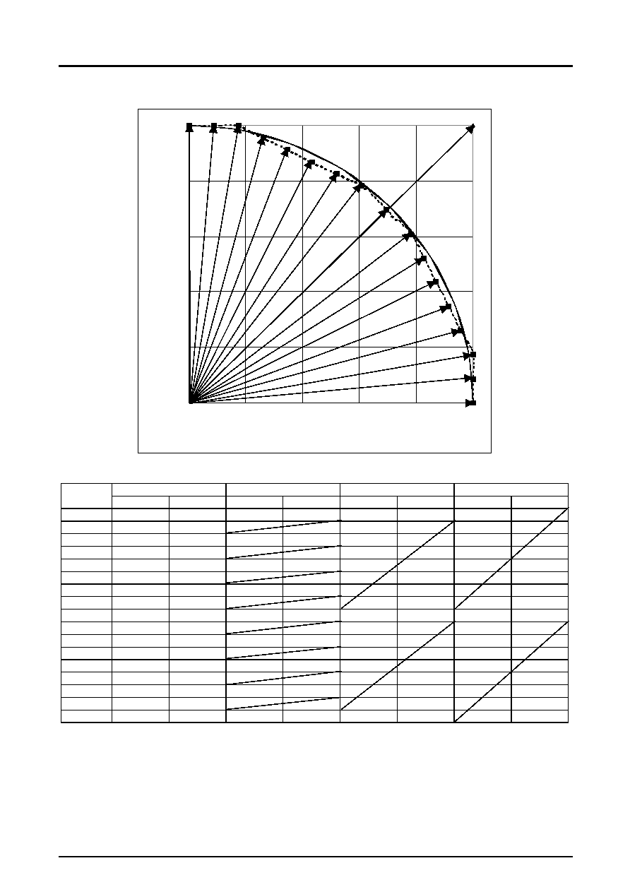
2W1-2 Phase Drive (D4 = 1, D3 = 0, D2 = 0: clockwise mode)
2W1-2 phase drive (channel 1 (channel 3): clockwise)
-100
-80
-60
-40
-20
0
20
40
60
80
100
0
10
20
30
11
(
%
)
2W1-2 phase drive (channel 2 (channel 4): clockwise)
-100
-80
-60
-40
-20
0
20
40
60
80
100
0
10
20
30
12
(
%
)
CLK
MO(initial)
MO(quarter)
LV8041FN
No.7944
-
14/24
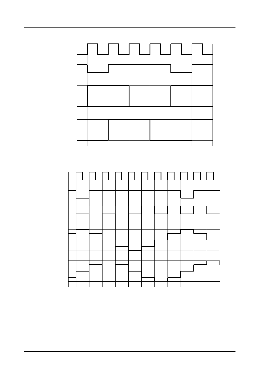
4W1-2 Phase Drive (D4 = 1, D3 = 1, D2 = 0: clockwise mode)
-100
-80
-60
-40
-20
0
20
40
60
80
100
0
10
20
30
40
50
60
11
(
)
-100
-80
-60
-40
-20
0
20
40
60
80
100
0
10
20
30
40
50
60
12 (
)
CLK
MO(initial)
MO(quarter)

LV8041FN
No.7944
-
15/24
Set Current Step Switching (CLK pin), Forward/Reverse Switching (D2 (F/R)) Basic Operation
CLK
D2 (F/R)
Channel
1 output
Channel
2 output
Position
number
Clockwise mode
Clockwise mode
Counter-
clockwise
mode
The IC internal D/A converter advances by one bit on the rising edge of each input clock pulse.
The clockwise/counterclockwise direction mode is switched by the D2 (F/R) data bit, and the direction in which the
position number advances is changed by switching this mode.
In clockwise mode, the channel 2 current phase is delayed by 90� as seen from the channel 1 current.
In counterclockwise mode, the channel 2 current phase leads by 90� as seen from the channel 1 current.
Output Enable (D7) and Reset (D6) Operational Description
0%
CLK
RST(D6)
Channel
1 output
Channel
2 output
MO
Initial mode
CLK
OE(D7)
Channel
1 output
Channel
2 output
MO
The outputs are in the high-impedance state
0%
Power saving
mode
When OE (D7) is set to 0, the outputs will be turned off on the next clock rising edge and set to the high-impedance
state. However, since the internal logic circuits continue to operate, the position number will advance if the clock signal
is input. Therefore, when OE (D7) is returned to 1, the IC will output levels according to the position number that has
been advanced by the clock input.
When RST (D6) is set to 0, the outputs are set to the initial state at the next clock rising edge, and the MO output goes
to the low level. When RST (D6) is set to one after that, the operation starts from the initial state on the next clock
input, and the position number begins advancing.
LV8041FN
No.7944
-
16/24
Hold Bit (D5) Operational Description
Internal logic
(External) clock
Internal clock
HOLD(D5)
logic
logic
(External)
clock
HOLD (D5)
Channel
1 output
Channel
2 output
Internal
clock
Held at the
low level
0%
Held at the
high level
Hold state
Hold state
Step/hold
(1)
Step/hold
release
Step/hold
(2)
Step/hold
release
When the HOLD bit (D5) is set to 1, the internal clock signal is held at the state of the external clock at that point.
Since the external clock is low at the timing of the step/hold (1) operation in the figure, the internal clock is then held at
the low level. Similarly, since the external clock is high at the timing of the step/hold (2) operation in the figure, the
internal clock is then held at the high level.
When the HOLD bit (D5) is set to 0, the internal clock is synchronized with the normal (external) clock.
The outputs retain their states at the time the step/hold operation was input, and after the step/hold is released, they
proceed with the timing of the next input clock rising edge.
As long as the IC is in the hold state, the position number will not be advanced even if the external clock signal is input.
LV8041FN
No.7944
-
17/24
Current Control Operation Specifications
Sine Wave Increasing Direction
Coil current
fchop
Set current
CHARGE
CLK
Set current
SLOW FAST
Current
mode
CHARGE SLOW
FAST
Sine Wave Decreasing Direction
Each current mode operates with the following sequence.
C o il c u rre n t
fc h o p
S e t c u rre n t
C H A R G E
C L K
S e t c u rre n t
S L O W FA S T
C u rre n t
m o d e
C H A R G E FA S T
S L O W
C H A R G E
The IC goes to charge mode during chopping oscillation startup. (A period in which the IC forcibly operates in
charge mode exists as 1/8 of a single chopping period regardless of the relationship between the magnitudes of the
coil current (ICOIL) and the set current (IREF).)
During charge mode, the IC compares the coil current (ICOIL) and the set current (IREF).
If the ICOIL < IREF state occurs during charge mode:
Charge mode continues until ICOIL IREF. After that, the IC switches to slow decay mode and then switches to
fast decay mode for the last 1/8 of a single chopping period.
If the ICOIL < IREF state does not occur during charge mode:
The IC switches to fast decay mode and the coil current is attenuated in fast decay mode until the end of the
single chopping period.
The IC repeats the above operation. Normally, in the sine wave increasing direction, the IC operates in slow (+ fast)
decay mode, and in the sine wave decreasing direction, the IC operates in fast decay mode until the current is attenuate
to the set level, and then the IC operates in slow decay mode.
LV8041FN
No.7944
-
18/24
Setting the Chopping Frequency (fchop)
When this IC performs constant current control, it uses a chopping operation based on a frequency set by an
external resistor.
The chopping frequency set by the value of the resistor connected to the R pin (pin 24) is set as shown in the figure
below.
0
50
100
150
200
250
300
0
10
20
30
40
50
60
70
80
90
100
R' � Ri
k �j
`bs"O
�"g
"
We recommend that a frequency in the range 50 kHz to 200 kHz be used.
Serial Data Truth Table for Monitor Output Settings (Monitor/channel 5 and 6 drive mode settings
register)
MO12 Output Setting: 2 bits
D3(MO_SELECT2)
D2(MO_SELECT1)
MO12 output state
0
0
The STP1 monitor is output
0
1
The STP2 monitor is output
1
0
The STP3 monitor is output (If PWM/MICRO is 1.)
1
1
A fixed high level is output
The MO12 pin can be set up to output any of the stepping motor driver states shown in the table above with the monitor
settings register settings shown in that table.
Monitor Output Mode Setting: 3 bits
D6 (MO56_MD)
D5 (MO34_MD)
D4 (MO12_MD)
Monitor output mode state
0
A low level is output from MO12 in the STP1 initial state
(Only when (D3, D2) (0, 0))
1
A low level is output from MO12 each STP1 1/4 period
(Only when (D3, D2) (0, 0))
0
A low level is output from MO34 in the STP2 initial state
(When (D3, D2) (0, 1) this is also output from MO12)
1
A low level is output from MO34 each STP2 1/4 period
(When (D3, D2) (0, 1) this is also output from MO12)
0
A low level is output from MO56 in the STP3 initial state
(When (D3, D2) (1, 0) this is also output from MO12)
1
A low level is output from MO56 each STP3 1/4 period
(When (D3, D2) (1, 0) this is also output from MO12)
Note : Don't Care
The stepping motor driver monitor outputs can be switched between a mode in which an output is only provided in the
initial position and a mode in which an output is provided each 1/4 period by setting the monitor setting register as
shown in the table above.
Resistance, R (k )
Chopping frequency
(kHz)
LV8041FN
No.7944
-
19/24
PWM Drive Forward/Reverse Motor Driver (Channels 5 and 6)
Drive Mode Setting Serial Data Truth Table: 1 bit (Monitor/channel 5 and 6 drive mode settings register)
Pin functions
D7(PWM/MICRO)
Operating mode
Pin 25
Pin 26
Low
PWM: 2 systems
PWM5
PWM6
High
One microstep drive STP system
CLK56
MO56
The circuit operating mode can be switched between direct PWM drive H bridge drive operation and 2W1-2 phase
microstep drive stepping motor drive operation by setting the D7 bit (PWM/MAICRO) as shown in the table above.
PWM Drive Mode (Channels 5 and 6 drive mode setting register bit D7 = 0)
Truth Table (Channels 5 and 6 driver settings register)
Inputs
Outputs
ST
PWM5
(PWM6)
D2
(D4)
D3
(D5)
OUTA
OUTB
Operating mode
Charge pump
circuit
Low
OFF
OFF
Standby mode
Stopped
High
High
Low
High
Low
Clockwise (forward)
High
High
High
Low
High
Counterclockwise (reverse)
High
Low
Low
OFF
OFF
Fast decay (output off)
High
Low
High
Low
Low
Slow decay (short-circuit braking)
Operating
Note : Don't care
Output Stage Transistor Functions
VM
U1
L1 L2
U2
ON
OFF
ON
OFF
OUTA OUTB
OFF
VM
U1
L1 L2
U2
ON
OFF
ON
OUTA
OUTB
VM
U1
L1 L2
U2
ON
OFF
ON
OFF
OUTA OUTB
(Forward)
(Reverse)
(Brake)
Forward/Reverse Output Operation Timing Chart (D3 = 0)
D2 data
PW M5
U1
L1
U2
L2
OFF
OFF
OFF
OFF
ON
ON
ON
ON
Forward
High
impedance
Forward
Reverse Reverse
High
impedance
High
impedance
"L"
"H"

LV8041FN
No.7944
-
20/24
Brake Mode Output Operation Timing Chart (D3 = 1)
D2 data
PWM5
U1
L1
U2
L2
OFF
OFF
ON
ON
ON
Forward
Forward
Reverse
Brake
Brake
Brake
Reverse
Brake
ON
OFF
OFF
"L" "H"
Microstep Drive Mode (Channels 5 and 6 drive mode setting register bit D7 = 1)
Clock Function (STP3)
Input
ST
CLK56
Operating mode
Charge pump circuit
Low
Standby mode
Stopped
High
Drive step mode
High
Drive step hold
Operating
STP State Setting Serial Data Truth Table: 4 bits (Channels 5 and 6 driver settings register)
D5 (OE3)
D4 (RES3)
D3 (HOLD3)
D2 (F/R3)
Operating mode
0
Clockwise (forward)
1
Counterclockwise (reverse)
0
Step/hold clear
1
Step/hold
0
Counter reset (Drive goes to the initial position)
1
Counter reset release
0
Outputs: high impedance
1
Output operating state
Note : Don't Care
Initial Drive Position
Initial mode
Drive mode
5ch
6ch
2W1-2 phase drive
100%
0%
Reference Voltage Setting Serial Data: 2 bits (Channels 5 and 6 driver settings register)
D7 (VSEN2)
D6 (VSEN1)
Current control reference voltage (when 100%)
0
0
0.2 V
0
1
0.134 V
1
0
0.1 V
1
1
0.066 V
Set Current Calculation
I
OUT
(reference voltage set current ratio)/(sense resistor (SEN) value)
Since the reference voltage can be set to either 0.2, 0.134, 0.1, or 0.066 V with the serial data, the output current
can be set with either the reference voltage or the value of the sense resistor SEN.
LV8041FN
No.7944
-
21/24
Constant Current Forward/Reverse Motor Driver (Channel 7)
Truth Table
Inputs
Outputs
ST
IN71
IN72
OUT7A
OUT7B
Mode
Charge pump circuit
Low
OFF
OFF
Standby mode
Stopped
High
Low
Low
OFF
OFF
Outputs off
High
Low
High
High
Low
Forward
High
High
Low
Low
High
Reverse
High
High
High
Low
Low
Brake
Operating
Note : Don't care
IN71
IN72
VM7
OUT7AA
OUT7BA
Reference
voltage
Fast
charge
circuit
Fast
discharge
circuit
FC7
SEN7
Lo
gic
c
i
rc
uit
s
VREF7
LIM7
OFF
OFF
High
impedance
IN71
IN72
U1
L1
U2
L2
OFF
OFF
Forward
ON
ON
ON
ON
Reverse
Brake
ON
High
impedance
Set Current Calculation
I
OUT
= LIM7 voltage/SEN7 resistor
Since the LIM7 voltage is an external input, the reference voltage can be set arbitrarily.
The reference voltage can be set to 0.2 V by using the VREF7 pin and shorting it to the LIM7 pin. If a voltage
created by resistor dividing the VREF7 voltage is input to LIM7, the reference voltage can be made variable (to
voltages under 0.2 V).
LV8041FN
No.7944
-
22/24
Recommended Application Circuit
The values shown near the various pins are recommended values. See the Allowable Operating Ranges table earlier in
this document for numerical values for the input conditions.
Channels 1 and 2: Microstep drive
Channels 3 and 4: Microstep drive
Channels 5 and 6: Described separately
Channel 7: Constant current drive
1
0.
1
F
10 F
0.
1
F
0.
01
F
PGND
12
PGND
34
OUT5A
OUT1A
41
42
45
44
46
50
52
51
49
48
47
43
8
9
10
11
12
6
7
4
5
2
3
1
21
14
15
16
17
18
19
20
22
23
24
25
38
37
39
28
30
29
31
33
32
34
36
35
40
26
27
13
LV8041FN
SEN1
OUT1B
VM12
OUT2A
SEN2
OUT2B
OUT3A
SEN3
OUT3B
VM34
OUT4A
SEN4
OUT
4
B
CLK34
M
O
34
ST
GND
DAT
A
ST
B
SCLK
VCC
R
PW
M
5
/
CLK56
PW
M
6
/
M
O
56
SEN5
OUT5B
VM56
OUT6A
SEN6
OUT6B
PGND7
OUT7A
SEN7
OUT7B
VM7
CPL1
CLK12
MO
1
2
IN
72
IN
71
VREF7
LIM
7
FC
7
VGH
CPH
2
CPH
1
VGL
CPL2
1
1
1
10 F
10 F
0.
1
F
0.1 F
0.1 F
1
10 F
20
k
5 V
0 V
10
k
10
k
5 V
0 V
5 V
0 V
5 V
0 V
Serial data input
5 V
0 V
M
M
5 V
5 V
5 V
5 V
5 V
The circuit diagram for
the section enclosed in
the dotted line is
provided separately.
( 1)
( 2)
( 3)
Note 1: Use a single point ground for the ground lines if at all possible.
2: Here, a 1 resistor is attached for each of the SEN pin resistors. This sets an output of 200 mA when the current ratio is 100%.
3: The LIM7 reference voltage can be provided either as an external voltage or by using VREF7: either voltage dividing VREF7 (0.2 V) or simply
shorting LIM7 to VREF7.
LV8041FN
No.7944
-
23/24
Channels 5 and 6 Recommended Circuit
The channels 5 and 6 systems can be switched between microstep drive and PWM drive.
Set the mode using the serial data as described earlier in this document.
Application 1 ... Microstep Drive Mode (Fixed 2W1-2 phase drive)
OUT5A
25
28
30
29
31
33
32
26
27
PW
M
5
/
C
L
K56
PW
M
6
/
M
O
56
SEN5
OUT5B
VM56
OUT6A
SEN6
OUT6B
1
1
M
5 V
0 V
( 4)
Note 4: In microstep drive mode, pin 26 functions as a position detection monitor pin.
Application 2 ... PWM Drive Mode (1)
OUT5A
25
28
30
29
31
33
32
26
27
PW
M
5
/
CL
K
5
6
PW
M
6
/
MO
5
6
SEN5
OUT5B
VM56
OUT6A
SEN6
OUT6B
5 V
0 V
5 V
0 V
( 5)
Note 5: Since the current limiter does not operate in PWM drive mode, the sense resistor is not needed.

LV8041FN
No.7944
-
24/24
Application (3) PWM Drive Mode (2) (Doubled output capacity)
OUT5A
25
28
30
29
31
33
32
26
27
PW
M
5
/
CL
K
5
6
PW
M
6
/
MO
5
6
SEN5
OUT5B
VM56
OUT6A
SEN6
OUT6B
5 V
0 V
( 6)
Note 6: Short the inputs together.
(Also short the outputs together. Do not short the outputs incorrectly: short OUT5A to OUT6A and short OUT5B to OUT6B.)
Specifications of any and all SANYO products described or contained herein stipulate the performance,
characteristics, and functions of the described products in the independent state, and are not guarantees
of the performance, characteristics, and functions of the described products as mounted in the customer's
products or equipment. To verify symptoms and states that cannot be evaluated in an independent
device, the customer should always evaluate and test devices mounted in the customer's products or
equipment.
SANYO Electric Co., Ltd. strives to supply high-quality high-reliability products. However, any and all
semiconductor products fail with some probability. It is possible that these probabilistic failures could give
rise to accidents or events that could endanger human lives, that could give rise to smoke or fire, or that
could cause damage to other property. When designing equipment, adopt safety measures so that these
kinds of accidents or events cannot occur. Such measures include but are not limited to protective circuits
and error prevention circuits for safe design, redundant design, and structural design.
In the event that any or all SANYO products (including technical data, services) described or contained
herein are controlled under any of applicable local export control laws and regulations, such products
must not be exported without obtaining the export license from the authorities concerned in accordance
with the above law.
No part of this publication may be reproduced or transmitted in any form or by any means, electronic or
mechanical, including photocopying and recording, or any information storage or retrieval system, of
otherwise, without the prior written permission of SANYO Electric Co., Ltd.
Any and all information described or contained herein are subject to change without notice due to
product/technology improvement, etc. When designing equipment, refer to the "Delivery Specification" for
the SANYO product that you intend to use.
Information (including circuit diagrams and circuit parameters) herein is for example only; it is not
guaranteed for volume production. SANYO believes information herein is accurate and reliable, but no
guarantees are made or implied regarding its use or any infringements of intellectual property rights or
This catalog provides information as of August, 2004. Specifications and information herein are subject to
change without notice.