 | –≠–ª–µ–∫—Ç—Ä–æ–Ω–Ω—ã–π –∫–æ–º–ø–æ–Ω–µ–Ω—Ç: FH201 | –°–∫–∞—á–∞—Ç—å:  PDF PDF  ZIP ZIP |
Any and all SANYO products described or contained herein do not have specifications that can handle
applications that require extremely high levels of reliability, such as life-support systems, aircraft's
control systems, or other applications whose failure can be reasonably expected to result in serious
physical and/or material damage. Consult with your SANYO representative nearest you before using
any SANYO products described or contained herein in such applications.
SANYO assumes no responsibility for equipment failures that result from using products at values that
exceed, even momentarily, rated values (such as maximum ratings, operating condition ranges,or other
parameters) listed in products specifications of any and all SANYO products described or contained
herein.
NPN Epitaxial Planar Silicon Composite Transistor
VCO OSC Circuit Applications
Ordering number:ENN6117
FH201
SANYO Electric Co.,Ltd. Semiconductor Company
TOKYO OFFICE Tokyo Bldg., 1-10, 1 Chome, Ueno, Taito-ku, TOKYO, 110-8534 JAPAN
N0199TS (KOTO) TA-1315 No.6117≠1/8
0 to 0.1
0.65
2.0
1.25
0.425
0.425
2.1
0.25
1
2
5
4
0.15
0.9
0.2
0.2
3
6
Specifications
Absolute Maximum Ratings
at Ta = 25∞C
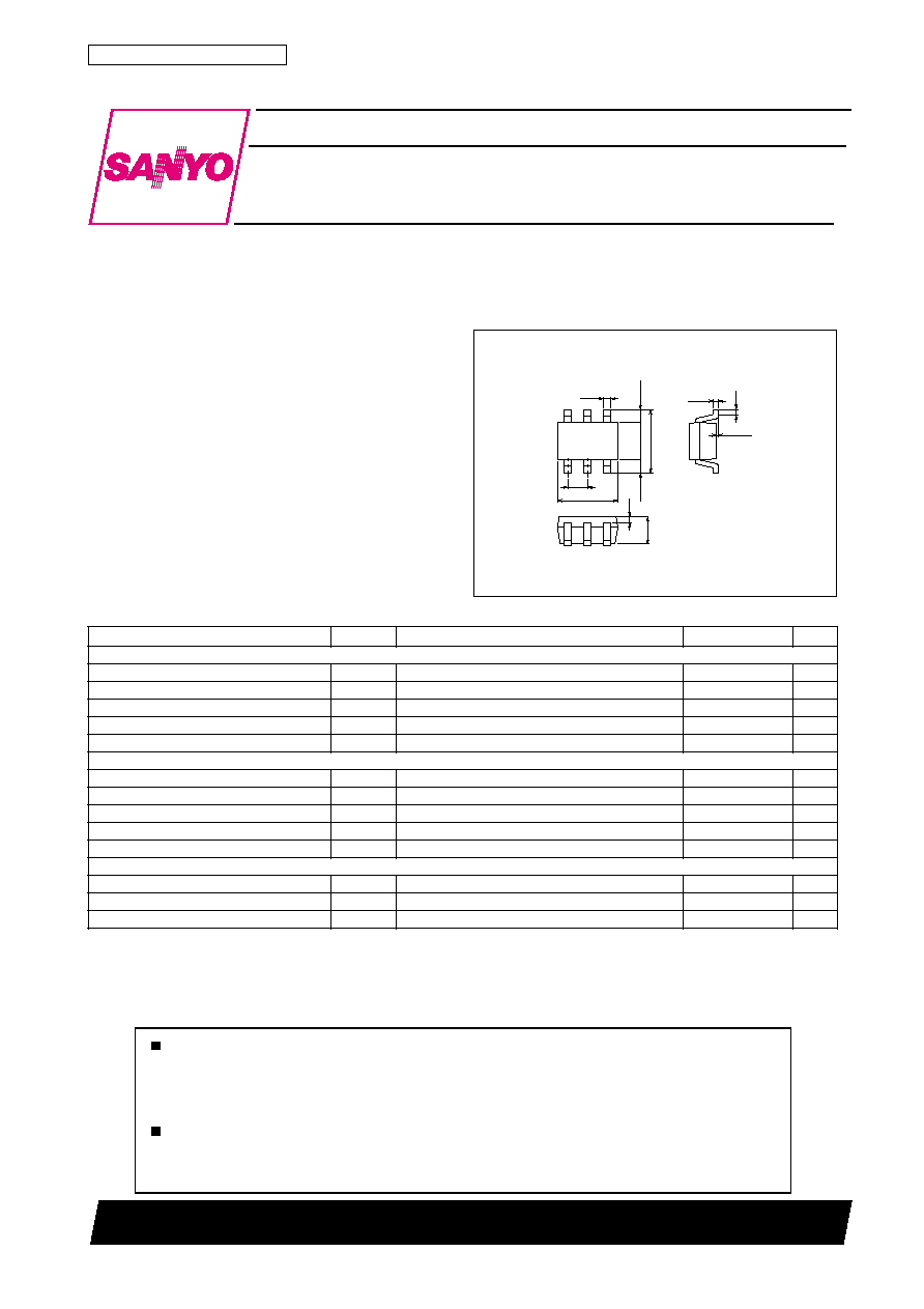
Package Dimensions
unit:mm
2149
[FH201]
Features
∑ Composite type with a buffer transistor (2SC4871)
and a oscillator transistor (2SC4867) contained in
the currently provided MCP package as a VCO
oscillator, improving the mounting efficiency greatly.
∑ The FH201 is formed with two chips, being equiva-
lent to the 2SC4871 and 2SC4867, placed in one
package.
∑ Optimal for use in UHF band oscillator circuit.
∞C
∞C
1 : Collector1
2 : Emitter1
3 : Collector2
4 : Emitter2
5 : Base2
6 : Base1
SANYO : MCP6
r
e
t
e
m
a
r
a
P
l
o
b
m
y
S
s
n
o
i
t
i
d
n
o
C
s
g
n
i
t
a
R
t
i
n
U
]
1
7
8
4
C
S
2
[
1
r
T
e
g
a
t
l
o
V
e
s
a
B
-
o
t
-
r
o
t
c
e
ll
o
C
V
O
B
C
6
1
V
e
g
a
t
l
o
V
r
e
t
t
i
m
E
-
o
t
-
r
o
t
c
e
ll
o
C
V
O
E
C
8
V
e
g
a
t
l
o
V
e
s
a
B
-
o
t
-
r
e
t
t
i
m
E
V
O
B
E
5
.
1
V
t
n
e
r
r
u
C
r
o
t
c
e
ll
o
C
IC
0
2
A
m
n
o
i
t
a
p
i
s
s
i
D
r
o
t
c
e
ll
o
C
PC
0
5
1
W
m
]
7
6
8
4
C
S
2
[
2
r
T
e
g
a
t
l
o
V
e
s
a
B
-
o
t
-
r
o
t
c
e
ll
o
C
V
O
B
C
6
1
V
e
g
a
t
l
o
V
r
e
t
t
i
m
E
-
o
t
-
r
o
t
c
e
ll
o
C
V
O
E
C
8
V
e
g
a
t
l
o
V
e
s
a
B
-
o
t
-
r
e
t
t
i
m
E
V
O
B
E
5
.
1
V
t
n
e
r
r
u
C
r
o
t
c
e
ll
o
C
IC
0
5
A
m
n
o
i
t
a
p
i
s
s
i
D
r
o
t
c
e
ll
o
C
PC
0
5
1
W
m
]
s
n
o
i
t
a
c
i
f
i
c
e
p
s
n
o
m
m
o
C
[
n
o
i
t
a
p
i
s
s
i
D
l
a
t
o
T
PT
0
0
2
W
m
e
r
u
t
a
r
e
p
m
e
T
n
o
i
t
c
n
u
J
j
T
0
5
1
e
r
u
t
a
r
e
p
m
e
T
e
g
a
r
o
t
S
g
t
s
T
0
5
1
+
o
t
5
5
≠

FH201
No.6117≠2/8
Electrical Characteristics
at Ta = 25∞C
Marking : 201
Electrical Connection
B2
B1
Tr1
Tr2
E2
C1
E1
C2
r
e
t
e
m
a
r
a
P
l
o
b
m
y
S
s
n
o
i
t
i
d
n
o
C
s
g
n
i
t
a
R
t
i
n
U
n
i
m
p
y
t
x
a
m
]
1
7
8
4
C
S
2
[
1
r
T
t
n
e
r
r
u
C
f
f
o
t
u
C
r
o
t
c
e
ll
o
C
I
O
B
C
V B
C
I
,
V
0
1
=
E 0
=
0
.
1
A
µ
t
n
e
r
r
u
C
f
f
o
t
u
C
r
e
t
t
i
m
E
I
O
B
E
V B
E
I
,
V
1
=
C 0
=
0
1
A
µ
n
i
a
G
t
n
e
r
r
u
C
C
D
h E
F
V E
C
I
,
V
5
=
C
A
m
4
=
0
9
0
8
1
t
c
u
d
o
r
P
h
t
d
i
w
d
n
a
B
-
n
i
a
G
fT
V E
C
I
,
V
5
=
C
A
m
4
=
0
1
z
H
G
e
c
n
a
t
i
c
a
p
a
C
t
u
p
t
u
O
b
o
C
V B
C
z
H
M
1
=
f
,
V
0
1
=
4
.
0
7
.
0
F
p
n
i
a
G
r
e
f
s
n
a
r
T
d
r
a
w
r
o
F
|
e
1
2
S
|
2
V E
C
I
,
V
5
=
C
z
H
G
1
=
f
,
A
m
7
=
0
1
3
1
B
d
e
r
u
g
i
F
e
s
i
o
N
F
N
V E
C
I
,
V
5
=
C
z
H
G
1
=
f
,
A
m
4
=
3
.
1
8
.
2
B
d
]
7
6
8
4
C
S
2
[
2
r
T
t
n
e
r
r
u
C
f
f
o
t
u
C
r
o
t
c
e
ll
o
C
I
O
B
C
V B
C
I
,
V
0
1
=
E 0
=
0
.
1
A
µ
t
n
e
r
r
u
C
f
f
o
t
u
C
r
e
t
t
i
m
E
I
O
B
E
V B
E
I
,
V
1
=
C 0
=
0
1
A
µ
n
i
a
G
t
n
e
r
r
u
C
C
D
h E
F
V E
C
I
,
V
5
=
C
A
m
5
1
=
0
9
0
8
1
t
c
u
d
o
r
P
h
t
d
i
w
d
n
a
B
-
n
i
a
G
fT
V E
C
I
,
V
5
=
C
A
m
5
1
=
0
.
9
z
H
G
e
c
n
a
t
i
c
a
p
a
C
t
u
p
t
u
O
b
o
C
V B
C
z
H
M
1
=
f
,
V
0
1
=
6
.
0
1
.
1
F
p
n
i
a
G
r
e
f
s
n
a
r
T
d
r
a
w
r
o
F
|
e
1
2
S
|
2
V E
C
I
,
V
5
=
C
z
H
G
1
=
f
,
A
m
5
1
=
0
1
3
1
B
d
e
r
u
g
i
F
e
s
i
o
N
F
N
V E
C
I
,
V
5
=
C
z
H
G
1
=
f
,
A
m
5
=
2
.
1
5
.
2
B
d
5
Cre -- VCB
5
3
2
1.0
7
0.1
7
5
3
2
5
7
0.1
2
3
5
7 1.0
2
3
2
3
5
7 10
5
5
3
2
1.0
7
0.1
7
5
3
2
7
0.1
2
3
5
7 1.0
2
3
2
3
5
7 10
5
Cob -- VCB
3
2
100
7
5
3
2
10
7
5
0.1
2
3
5
7 1.0
2
3
5
7
10
2
3
5
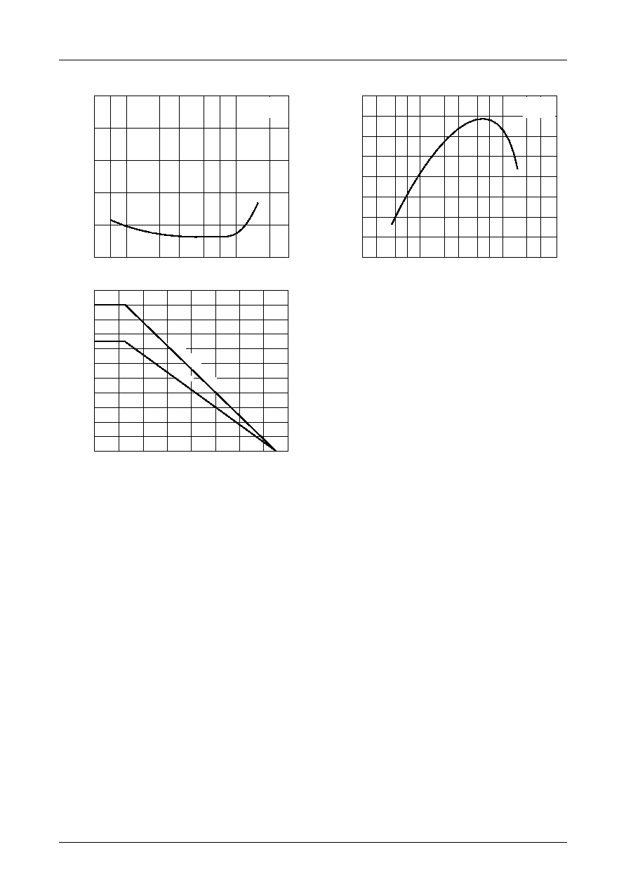
hFE -- IC
VCE=5V
[Tr1]
[Tr1]
[Tr1]
[Tr1]
f=1MHz
f=1MHz
2
10
7
5
7
5
3
2
1.0
3
3
5
1.0
2
3
5
7
2
3
7
10
fT -- IC
VCE=5V
IT00335
IT00336
IT00337
IT00338
DC Current Gain,
h
FE
Gain-Bandwidth Produnt,
f T
≠
GHz
Collector Current, IC ≠ mA
Collector Current, IC ≠ mA
Collector-to-Base Voltage, VCB -- V
Re
v
erse
T
ransfer Capacitance, Cre
≠
p
F
Collector-to-Base Voltage, VCB -- V
Output Capacitance, Cob
≠
p
F
FH201
No.6117≠3/8
2
4
6
8
10
0
1.0
5
7
10
2
3
5
7
2
3
S21e
2
-- IC
10
12
14
16
8
6
4
2
0
NF -- IC
VCE=5V
f=1GHz
VCE=5V
f=1GHz
2
3
5
7
1.0
2
3
5
7
10
2
3
5
[Tr1]
[Tr1]
[Tr1]
120
80
60
100
40
220
180
160
150
200
140
20
0
0
160
140
120
100
80
60
40
20
PC -- Ta
IT00339
IT00341
IT00340
Noise Figure, NF
≠
d
B
Collector Current, IC ≠ mA
Collector Current, IC ≠ mA
F
orw
ard
T
ransfer Gain,
S21e
2
≠d
B
Total dissipation
1 unit
Ambient Temperature, Ta ≠
∞
C
Collector Dissipation, P
C
≠
mW
FH201
No.6117≠4/8
S parameter [Tr1]
j50
j25
j10
0
10
25
--j10
--j25
--j50
--j100
--j150
--j200
--j250
j100
j150
j200
j250
100
150
250
V
CE =5V
IC=7mA
VCE=5V
IC=2mA
2.0GHz
2.0GHz
0.2GHz 0.2GHz
50
IT00342
90
∞
120
∞
150
∞
±
180
∞
--150
∞
--120
∞
--90
∞
--30
∞
--60
∞
0
60
∞
30
∞
10
8
6
4
2
0.2GHz
0.2GHz
2.0GHz
2.0GHz
V
CE =5V
IC=7mA
V CE
=5V
I C
=2mA
IT00343
90
∞
120
∞
150
∞
±
180
∞
--150
∞
--120
∞
--90
∞
--30
∞
--60
∞
0
60
∞
30
∞
0.04 0.08 0.12 0.16 0.2
0.2GHz
0.2GHz
2.0GHz
2.0GHz
V CE
=5V
I C
=2mA
V
CE
=5V
I C
=7mA
IT00344
j50
j25
j10
0
10
25
--j10
--j25
--j50
--j100
--j150
--j200
--j250
j100
j150
j200
j250
100
150
250
VCE=5V
IC=7mA
VCE=5V
IC=2mA
2.0GHz
2.0GHz
0.2GHz
0.2GHz
50
IT00345
VCE=5V
f=200MHz to 2000MHz(200MHz Step)
S11e
VCE=5V
f=200MHz to 2000MHz(200MHz Step)
S12e
VCE=5V
f=200MHz to 2000MHz(200MHz Step)
S22e
VCE=5V
f=200MHz to 2000MHz(200MHz Step)
S21e
FH201
No.6117≠5/8
S Parameters (Common emitter) [Tr1]
V
CE
=5V, I
C
=2mA, Z
O
=50
V
CE
=5V, I
C
=7mA, Z
O
=50
)
z
H
M
(
q
e
r
F
S
|
1
1 |
S 1
1
S
|
1
2 |
S 1
2
S
|
2
1 |
S 2
1
S
|
2
2 |
S 2
2
0
0
2
2
1
9
.
0
6
.
7
1
≠
4
6
7
.
5
5
.
1
6
1
4
3
0
.
0
0
.
9
7
4
7
9
.
0
3
.
0
1
≠
0
0
4
5
3
8
.
0
0
.
3
3
≠
2
8
2
.
5
5
.
5
4
1
5
6
0
.
0
9
.
9
6
9
1
9
.
0
2
.
9
1
≠
0
0
6
2
4
7
.
0
9
.
6
4
≠
3
5
7
.
4
2
.
1
3
1
8
8
0
.
0
8
.
2
6
0
5
8
.
0
3
.
6
2
≠
0
0
8
9
4
6
.
0
9
.
8
5
≠
8
6
2
.
4
4
.
9
1
1
7
0
1
.
0
9
.
7
5
9
8
7
.
0
6
.
1
3
≠
0
0
0
1
8
7
5
.
0
7
.
8
6
≠
0
4
8
.
3
4
.
9
0
1
1
2
1
.
0
5
.
4
5
0
4
7
.
0
5
.
5
3
≠
0
0
2
1
2
1
5
.
0
1
.
8
7
≠
0
4
4
.
3
5
.
0
0
1
4
3
1
.
0
2
.
2
5
8
9
6
.
0
9
.
8
3
≠
0
0
4
1
5
4
4
.
0
3
.
6
8
≠
3
2
1
.
3
5
.
2
9
5
4
1
.
0
3
.
0
5
4
6
6
.
0
6
.
1
4
≠
0
0
6
1
0
0
4
.
0
0
.
3
9
≠
6
3
8
.
2
2
.
5
8
4
5
1
.
0
2
.
9
4
8
3
6
.
0
3
.
4
4
≠
0
0
8
1
9
5
3
.
0
5
.
8
9
≠
8
8
5
.
2
0
.
9
7
4
6
1
.
0
4
.
8
4
5
1
6
.
0
3
.
6
4
≠
0
0
0
2
9
1
3
.
0
6
.
6
0
1
≠
7
9
2
.
2
0
.
3
7
4
7
1
.
0
9
.
7
4
1
0
6
.
0
3
.
8
4
≠
)
z
H
M
(
q
e
r
F
S
|
1
1 |
S 1
1
S
|
1
2 |
S 1
2
S
|
2
1 |
S 2
1
S
|
2
2 |
S 2
2
0
0
2
1
2
7
.
0
1
.
5
3
≠
2
6
2
.
2
1
1
.
7
4
1
0
3
0
.
0
8
.
2
7
0
0
9
.
0
9
.
6
1
≠
0
0
4
5
5
5
.
0
9
.
9
5
≠
5
4
4
.
9
9
.
4
2
1
0
5
0
.
0
4
.
4
6
3
6
7
.
0
6
.
5
2
≠
0
0
6
8
2
4
.
0
5
.
7
7
≠
0
9
2
.
7
2
.
0
1
1
5
6
0
.
0
9
.
1
6
6
6
6
.
0
3
.
9
2
≠
0
0
8
4
4
3
.
0
9
.
9
8
≠
7
7
8
.
5
1
.
0
0
1
8
7
0
.
0
5
.
1
6
1
1
6
.
0
1
.
1
3
≠
0
0
0
1
1
9
2
.
0
6
.
0
0
1
≠
1
1
9
.
4
1
.
2
9
1
9
0
.
0
7
.
1
6
3
8
5
.
0
5
.
2
3
≠
0
0
2
1
4
5
2
.
0
9
.
0
1
1
≠
3
2
2
.
4
1
.
5
8
4
0
1
.
0
5
.
1
6
3
6
5
.
0
1
.
4
3
≠
0
0
4
1
1
2
2
.
0
4
.
1
2
1
≠
3
0
7
.
3
0
.
9
7
7
1
1
.
0
6
.
1
6
1
5
5
.
0
7
.
5
3
≠
0
0
6
1
7
9
1
.
0
9
.
8
2
1
≠
4
9
2
.
3
6
.
3
7
9
2
1
.
0
6
.
1
6
0
4
5
.
0
8
.
7
3
≠
0
0
8
1
8
7
1
.
0
7
.
6
3
1
≠
6
4
9
.
2
5
.
8
6
3
4
1
.
0
1
.
1
6
0
3
5
.
0
7
.
9
3
≠
0
0
0
2
1
7
1
.
0
6
.
8
4
1
≠
2
9
6
.
2
8
.
3
6
7
5
1
.
0
7
.
0
6
9
2
5
.
0
7
.
1
4
≠

FH201
No.6117≠6/8
5
2
4
6
8
10
0
1.0
10
2
3
5
5
7
7
7
2
3
S21e
2
-- IC
10
12
14
16
8
6
4
2
0
NF -- IC
VCE=5V
f=1GHz
VCE=5V
f=1GHz
Cre -- VCB
5
3
2
1.0
7
0.1
7
5
3
2
5
7
0.1
2
3
5
7 1.0
2
3
2
3
5
7 10
5
3
5
7
1.0
2
3
5
7
7
10
100
2
3
5
5
3
2
1.0
7
0.1
7
5
3
2
7 0.1
2
3
5
7 1.0
2
3
2
3
5
7 10
5
Cob -- VCB
3
2
100
7
5
3
2
10
7
5
3
5
7 1.0
2
3
5
7
7
10
100
2
2
3
5
hFE -- IC
VCE=5V
[Tr2]
[Tr2]
[Tr2]
[Tr2]
[Tr2]
[Tr2]
[Tr2]
f=1MHz
f=1MHz
2
10
7
5
7
5
3
2
1.0
3
5
1.0
2
3
5
5
7
7
2
3
7
10
100
fT -- IC
VCE=5V
120
140
160
150
180
200
220
80
60
100
40
20
0
0
160
140
120
100
80
60
40
20
PC -- Ta
IT00346
IT00347
IT00348
IT00349
IT00350
IT00352
IT00351
DC Current Gain,
h
FE
Gain-Bandwidth Product,
f T
≠
GHz
Collector Current, IC ≠ mA
Collector Current, IC ≠ mA
Collector-to-Base Voltage, VCB -- V
Re
v
erse
T
ransfer Capacitance, Cre
≠
pF
Collector-to-Base Voltage, VCB -- V
Output Capacitance, Cob
≠
pF
Noise Figure, NF
≠
d
B
Collector Current, IC ≠ mA
Collector Current, IC ≠ mA
F
orw
ard
T
ransfer Gain,
S21e
2
≠d
B
To
tal dissipation
1 unit
Ambient Temperature, Ta ≠
∞
C
Collector Dissipation, P
C
≠
mW

FH201
No.6117≠7/8
S parameter [Tr2]
j50
j25
j10
0
10
25
--j10
--j25
--j50
--j100
--j150
--j200
--j250
j100
j150
j200
j250
100
150
250
2.0GHz
I
C =15mA
I
C =5mA
2.0GHz
0.2GHz
0.2GHz
50
IT00353
90
∞
120
∞
150
∞
±
180
∞
--150
∞
--120
∞
--90
∞
--30
∞
--60
∞
0
60
∞
30
∞
20
16
12
8
4
0.2GHz
0.2GHz
2.0GHz
2.0GHz
IC=5mA
IC
=15mA
IT00354
90
∞
120
∞
150
∞
±
180
∞
--150
∞
--120
∞
--90
∞
--30
∞
--60
∞
0
60
∞
30
∞
0.04 0.08 0.12 0.16 0.2
0.2GHz
0.2GHz
2.0GHz
2.0GHz
I C
=15mA
I C
=5mA
IT00355
j50
j25
j10
0
10
25
--j10
--j25
--j50
--j100
--j150
--j200
--j250
j100
j150
j200
j250
100
150
250
2.0GHz
2.0GHz
50
IC=15mA
IC=5mA
IT00356
VCE=5V
f=200MHz to 2000MHz(200MHz Step)
S11e
VCE=5V
f=200MHz to 2000MHz(200MHz Step)
S12e
VCE=5V
f=200MHz to 2000MHz(200MHz Step)
S22e
VCE=5V
f=200MHz to 2000MHz(200MHz Step)
S21e

Specifications of any and all SANYO products described or contained herein stipulate the performance,
characteristics, and functions of the described products in the independent state, and are not guarantees
of the performance, characteristics, and functions of the described products as mounted in the customer's
products or equipment. To verify symptoms and states that cannot be evaluated in an independent device,
the customer should always evaluate and test devices mounted in the customer's products or equipment.
SANYO Electric Co., Ltd. strives to supply high-quality high-reliability products. However, any and all
semiconductor products fail with some probability. It is possible that these probabilistic failures could
give rise to accidents or events that could endanger human lives, that could give rise to smoke or fire,
or that could cause damage to other property. When designing equipment, adopt safety measures so
that these kinds of accidents or events cannot occur. Such measures include but are not limited to protective
circuits and error prevention circuits for safe design, redundant design, and structural design.
In the event that any or all SANYO products(including technical data,services) described or
contained herein are controlled under any of applicable local export control laws and regulations,
such products must not be expor ted without obtaining the expor t license from the author ities
concerned in accordance with the above law.
No part of this publication may be reproduced or transmitted in any form or by any means, electronic or
mechanical, including photocopying and recording, or any information storage or retrieval system,
or otherwise, without the prior written permission of SANYO Electric Co. , Ltd.
Any and all information described or contained herein are subject to change without notice due to
product/technology improvement, etc. When designing equipment, refer to the "Delivery Specification"
for the SANYO product that you intend to use.
Information (including circuit diagrams and circuit parameters) herein is for example only ; it is not
guaranteed for volume production. SANYO believes information herein is accurate and reliable, but
no guarantees are made or implied regarding its use or any infringements of intellectual property rights
or other rights of third parties.
This catalog provides information as of November, 1999. Specifications and information herein are subject
to change without notice.
FH201
PS No.6117≠8/8
S Parameters (Common emitter) [Tr2]
V
CE
=5V, I
C
=5mA, Z
O
=50
)
z
H
M
(
q
e
r
F
S
|
1
1 |
S 1
1
S
|
1
2 |
S 1
2
S
|
2
1 |
S 2
1
S
|
2
2 |
S 2
2
0
0
2
9
4
7
.
0
7
.
0
5
≠
9
2
2
.
2
1
6
.
1
4
1
4
4
0
.
0
4
.
5
6
7
4
8
.
0
4
.
5
2
≠
0
0
4
3
8
5
.
0
7
.
5
8
≠
0
0
9
.
8
1
.
8
1
1
8
6
0
.
0
3
.
4
5
5
5
6
.
0
4
.
7
3
≠
0
0
6
7
8
4
.
0
6
.
9
0
1
≠
6
3
6
.
6
7
.
3
0
1
1
8
0
.
0
6
.
1
5
8
3
5
.
0
3
.
2
4
≠
0
0
8
8
2
4
.
0
6
.
6
2
1
≠
6
7
2
.
5
9
.
3
9
3
9
0
.
0
6
.
1
5
3
7
4
.
0
4
.
4
4
≠
0
0
0
1
5
0
4
.
0
3
.
9
3
1
≠
9
7
3
.
4
9
.
5
8
6
0
1
.
0
6
.
2
5
3
4
4
.
0
2
.
6
4
≠
0
0
2
1
7
8
3
.
0
6
.
0
5
1
≠
1
3
7
.
3
7
.
8
7
7
1
1
.
0
6
.
3
5
1
2
4
.
0
1
.
8
4
≠
0
0
4
1
7
7
3
.
0
1
.
0
6
1
≠
8
5
2
.
3
6
.
2
7
0
3
1
.
0
4
.
4
5
5
0
4
.
0
6
.
9
4
≠
0
0
6
1
5
6
3
.
0
8
.
6
6
1
≠
4
2
9
.
2
5
.
7
6
2
4
1
.
0
2
.
5
5
3
9
3
.
0
1
.
2
5
≠
0
0
8
1
2
6
3
.
0
3
.
4
7
1
≠
9
8
5
.
2
9
.
1
6
6
5
1
.
0
6
.
5
5
7
8
3
.
0
3
.
4
5
≠
0
0
0
2
1
6
3
.
0
3
.
8
7
1
3
6
3
.
2
8
.
6
5
1
7
1
.
0
9
.
5
5
3
8
3
.
0
4
.
6
5
≠
V
CE
=5V, I
C
=7mA, Z
O
=50
)
z
H
M
(
q
e
r
F
S
|
1
1 |
S 1
1
S
|
1
2 |
S 1
2
S
|
2
1 |
S 2
1
S
|
2
2 |
S 2
2
0
0
2
7
0
5
.
0
6
.
1
8
≠
2
2
4
.
9
1
2
.
4
2
1
3
3
0
.
0
9
.
1
6
0
5
6
.
0
9
.
6
3
≠
0
0
4
2
8
3
.
0
5
.
9
1
1
≠
5
9
5
.
1
1
8
.
3
0
1
0
5
0
.
0
0
.
1
6
5
4
4
.
0
0
.
3
4
≠
0
0
6
1
4
3
.
0
9
.
0
4
1
≠
6
4
0
.
8
3
.
3
9
5
6
0
.
0
3
.
3
6
5
6
3
.
0
5
.
3
4
≠
0
0
8
2
3
3
.
0
0
.
4
5
1
≠
2
8
1
.
6
4
.
6
8
1
8
0
.
0
1
.
5
6
0
3
3
.
0
3
.
3
4
≠
0
0
0
1
0
2
3
.
0
0
.
3
6
1
≠
3
6
0
.
5
8
.
9
7
9
9
0
.
0
6
.
5
6
8
1
3
.
0
8
.
3
4
≠
0
0
2
1
6
1
3
.
0
9
.
0
7
1
≠
3
6
2
.
4
1
.
4
7
6
1
1
.
0
7
.
5
6
1
1
3
.
0
9
.
5
4
≠
0
0
4
1
5
1
3
.
0
0
.
8
7
1
≠
6
1
7
.
3
2
.
9
6
4
3
1
.
0
0
.
5
6
4
0
3
.
0
4
.
7
4
≠
0
0
6
1
4
1
3
.
0
7
.
6
7
1
0
7
2
.
3
3
.
4
6
0
5
1
.
0
4
.
4
6
7
9
2
.
0
3
.
0
5
≠
0
0
8
1
1
1
3
.
0
2
.
1
7
1
2
2
9
.
2
0
.
0
6
7
6
1
.
0
3
.
3
6
3
9
2
.
0
6
.
2
5
≠
0
0
0
2
3
1
3
.
0
4
.
5
6
1
6
5
6
.
2
9
.
5
5
6
8
1
.
0
1
.
2
6
5
9
2
.
0
8
.
4
5
≠