
52098HA (KT)/N2394TS (KOTO) BX-0370 No.4726-1/4
SANYO Electric Co.,Ltd. Semiconductor Bussiness Headquaters
TOKYO OFFICE Tokyo Bldg., 1-10, 1 Chome, Ueno, Taito-ku, TOKYO, 110-8534 JAPAN
TR:NPN Epitaxial Planar Silicon Transistor
SBD:Schottky Barrier Diode
DC-DC Converter Applications
Ordering number:EN4726
FP302
r
e
t
e
m
a
r
a
P
l
o
b
m
y
S
s
n
o
i
t
i
d
n
o
C
s
g
n
i
t
a
R
t
i
n
U
]
R
T
[
e
g
a
t
l
o
V
e
s
a
B
-
o
t
-
r
o
t
c
e
ll
o
C
V
O
B
C
0
6
V
e
g
a
t
l
o
V
r
e
t
t
i
m
E
-
o
t
-
r
o
t
c
e
ll
o
C
V
O
E
C
5
4
V
e
g
a
t
l
o
V
e
s
a
B
-
o
t
-
r
e
t
t
i
m
E
V
O
B
E
5
V
t
n
e
r
r
u
C
r
o
t
c
e
ll
o
C
IC
5
.
1
A
)
e
s
l
u
P
(
t
n
e
r
r
u
C
r
o
t
c
e
ll
o
C
I P
C
3
A
t
n
e
r
r
u
C
e
s
a
B
IB
0
0
3
A
m
n
o
i
t
a
p
i
s
s
i
D
r
o
t
c
e
ll
o
C
PC
8
.
0
W
e
r
u
t
a
r
e
p
m
e
T
n
o
i
t
c
n
u
J
j
T
0
5
1
e
r
u
t
a
r
e
p
m
e
T
e
g
a
r
o
t
S
g
t
s
T
0
5
1
+
o
t
5
5
≠
]
D
B
S
[
e
g
a
t
l
o
V
e
s
r
e
v
e
R
k
a
e
P
e
v
i
t
i
t
e
p
e
R
V
M
R
R
0
5
V
e
g
a
t
l
o
V
e
g
r
u
S
e
s
r
e
v
e
R
k
a
e
P
e
v
i
t
i
t
e
p
e
r
-
n
o
N
V
M
S
R
5
5
V
t
n
e
r
r
u
C
d
e
i
f
i
t
c
e
R
e
g
a
r
e
v
A
IO
0
0
5
A
m
t
n
e
r
r
u
C
d
r
a
w
r
o
F
e
g
r
u
S
I
M
S
F
e
l
c
y
c
1
,
e
v
a
w
e
n
i
s
z
H
0
5
5
A
e
r
u
t
a
r
e
p
m
e
T
n
o
i
t
c
n
u
J
j
T
5
2
1
+
o
t
5
5
≠
e
r
u
t
a
r
e
p
m
e
T
e
g
a
r
o
t
S
g
t
s
T
5
2
1
+
o
t
5
5
≠
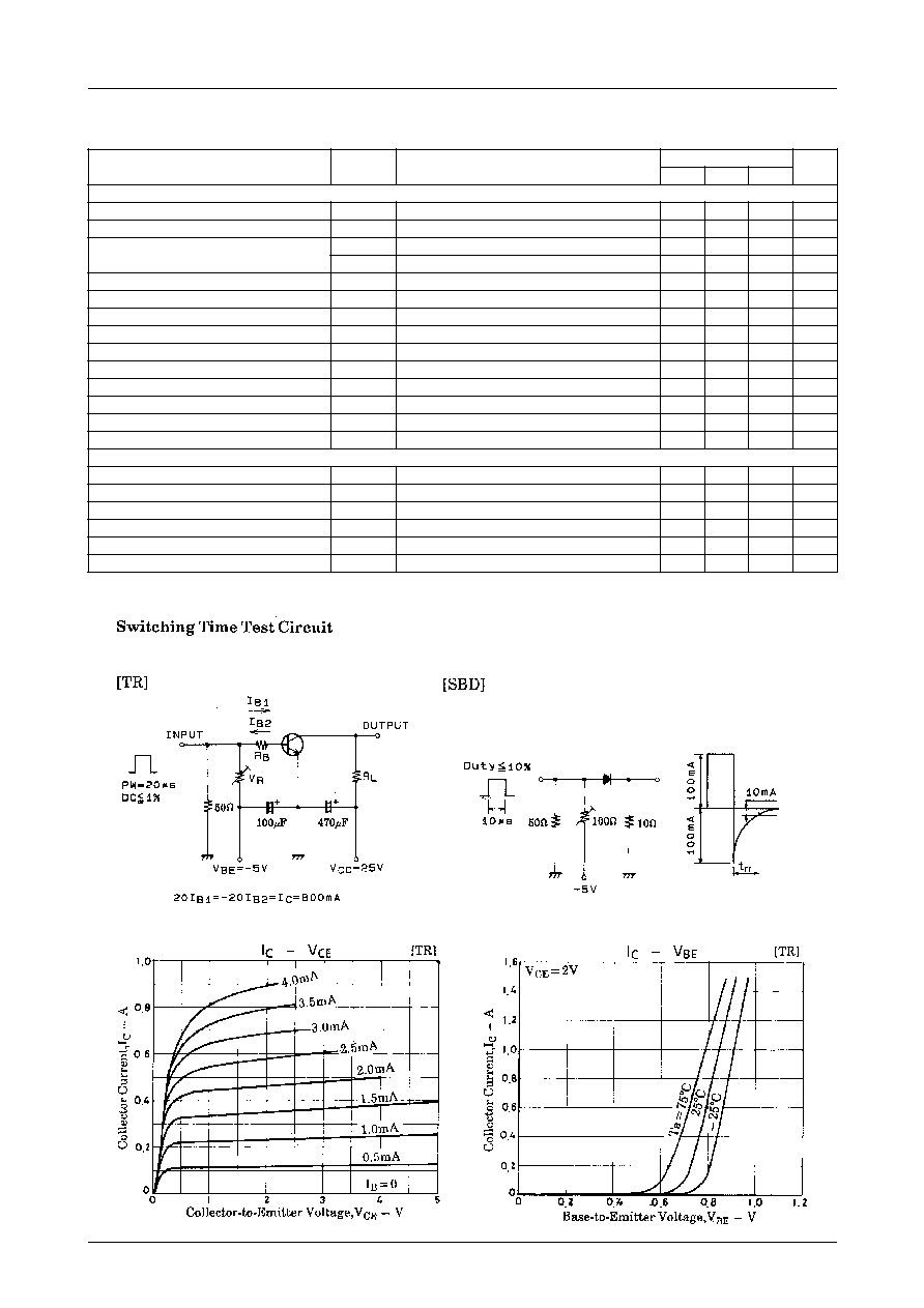
Specifications
Absolute Maximum Ratings
at Ta = 25∞C
Package Dimensions
unit:mm
2099A
[FP302]
Features
∑ Composite type with NPN transistor and Schottoky
barrier diode facilitating high-density mounting.
∑ The FP302 is composed of chips equivalent to the
2SC4520 and SB05-05CP, which are placed in one
package.
∞C
∞C
Mounted on ceramic board (250mm
2
◊
0.8mm)
1:Base
2:Collector
3:Emitter Common
4:Cathode
5:Anode
6:Cathode
7:Collector
SANYO:PCP5
(Bottom view)
∞C
Electrical Connection
Continued on next page.
∞C
1:Base
2:Collector
3:Emitter Common
4:Cathode
5:Anode
6:Cathode
7:Collector
(Top view)
FP302
No.4726-2/4
Continued from preceding page.
Electrical Characteristics
at Ta=25∞C
∞C/W
r
e
t
e
m
a
r
a
P
l
o
b
m
y
S
s
n
o
t
i
d
n
o
C
s
g
n
i
t
a
R
t
i
n
U
n
i
m
p
y
t
x
a
m
]
R
T
[
t
n
e
r
r
u
C
f
f
o
t
u
C
r
o
t
c
e
ll
o
C
I
O
B
C
V B
C
I
,
V
5
4
=
E 0
=
0
.
1
A
µ
t
n
e
r
r
u
C
f
f
o
t
u
C
r
e
t
t
i
m
E
I
O
B
E
V B
E
I
,
V
3
=
C 0
=
0
.
1
A
µ
n
i
a
G
t
n
e
r
r
u
C
C
D
h E
F 1
V E
C
I
,
V
2
=
C
A
m
0
0
1
=
0
0
1
0
0
4
h E
F 2
V E
C
I
,
V
2
=
C
A
5
.
1
=
0
4
t
c
u
d
o
r
P
h
t
d
i
w
d
n
a
B
-
n
i
a
G
fT
V E
C
I
,
V
2
=
C
A
m
0
0
1
=
0
0
3
z
H
M
e
c
n
a
t
i
c
a
p
a
C
t
u
p
t
u
O
b
o
C
V B
C
z
H
M
1
=
f
,
V
0
1
=
3
1
F
p
e
g
a
t
l
o
V
n
o
i
t
a
r
u
t
a
S
E
-
C
V
)
t
a
s
(
E
C
IC
I
,
A
m
0
0
8
=
B
A
m
0
4
=
5
2
.
0
7
.
0
V
e
g
a
t
l
o
V
n
o
i
t
a
r
u
t
a
S
E
-
B
V
)
t
a
s
(
E
B
IC
I
,
A
m
0
0
8
=
B
A
m
0
4
=
9
.
0
3
.
1
V
e
g
a
t
l
o
V
n
w
o
d
k
a
e
r
B
B
-
C
V
O
B
C
)
R
B
(
IC
I
,
A
µ
0
1
=
E 0
=
0
6
V
e
g
a
t
l
o
V
n
w
o
d
k
a
e
r
B
E
-
C
V
O
E
C
)
R
B
(
IC
R
,
A
m
1
=
E
B =
5
4
V
e
g
a
t
l
o
V
n
w
o
d
k
a
e
r
B
B
-
E
V
O
B
E
)
R
B
(
IE
I
,
A
µ
0
1
=
C 0
=
5
V
e
m
i
T
N
O
-
n
r
u
T
t n
o
t
i
u
c
r
i
C
t
s
e
T
d
e
i
f
i
c
e
p
s
e
e
S
0
5
s
n
e
m
i
T
e
g
a
r
o
t
S
t g
t
s
t
i
u
c
r
i
C
t
s
e
T
d
e
i
f
i
c
e
p
s
e
e
S
0
5
1
s
n
e
m
i
T
F
F
O
-
n
r
u
T
t ff
o
t
i
u
c
r
i
C
t
s
e
T
d
e
i
f
i
c
e
p
s
e
e
S
0
8
1
s
n
]
D
B
S
[
e
g
a
t
l
o
V
e
s
r
e
v
e
R
VR
IR
A
µ
0
0
2
=
0
5
V
e
g
a
t
l
o
V
d
r
a
w
r
o
F
VF
IF
A
m
0
0
5
=
5
5
.
0
V
t
n
e
r
r
u
C
e
s
r
e
v
e
R
IR
VR
V
5
2
=
0
5
A
µ
e
c
n
a
t
i
c
a
p
a
C
l
a
n
i
m
r
e
t
r
e
t
n
I
C
VR
e
l
c
y
c
z
H
M
1
=
f
,
V
0
1
=
2
2
F
p
e
m
i
T
y
r
e
v
o
c
e
R
e
s
r
e
v
e
R
t r
r
IF I
= R
.
t
i
u
c
r
i
C
t
s
e
T
d
e
i
f
i
c
p
e
s
e
e
S
,
A
m
0
0
1
=
0
1
s
n
e
c
n
a
t
s
i
s
e
R
l
a
m
r
e
h
T
a
-
j
h
t
R
0
7
1
Mounted on ceramic board (250mm
2
◊
0.8mm)

FP302
PS No.4726-4/4
No products described or contained herein are intended for use in surgical implants, life-support systems,
aerospace equipment, nuclear power control systems, vehicles, disaster/crime-prevention equipment and
the like, the failure of which may directly or indirectly cause injury, death or property loss.
Anyone purchasing any products described or contained herein for an above-mentioned use shall:
Accept full responsibility and indemnify and defend SANYO ELECTRIC CO., LTD., its affiliates,
subsidiaries and distributors and all their officers and employees, jointly and severally, against any
and all claims and litigation and all damages, cost and expenses associated with such use:
Not impose any responsibilty for any fault or negligence which may be cited in any such claim or
litigation on SANYO ELECTRIC CO., LTD., its affiliates, subsidiaries and distributors or any of
their officers and employees jointly or severally.
Information (including circuit diagrams and circuit parameters) herein is for example only; it is not guarant-
eed for volume production. SANYO believes information herein is accurate and reliable, but no guarantees
are made or implied regarding its use or any infringements of intellectual property rights or other rights of
third parties.
This catalog provides information as of May, 1998. Specifications and information herein are subject to
change without notice.
