 | –≠–ª–µ–∫—Ç—Ä–æ–Ω–Ω—ã–π –∫–æ–º–ø–æ–Ω–µ–Ω—Ç: LA17000M | –°–∫–∞—á–∞—Ç—å:  PDF PDF  ZIP ZIP |
Ordering number: ENN6522
SANYO Electric Co.,Ltd. Semiconductor Company
TOKYO OFFICE Tokyo Bldg., 1-10, 1 Chome, Ueno, Taito-ku, TOKYO, 110-8534 JAPAN
Any and all SANYO products described or contained herein do not have specifications that can handle
applications that require extremely high levels of reliability, such as life-support systems, aircraft's
control systems, or other applications whose failure can be reasonably expected to result in serious
physical and/or material damage. Consult with your SANYO representative nearest you before using
any SANYO products described or contained herein in such applications.
SANYO assumes no responsibility for equipment failures that result from using products at values that
exceed, even momentarily, rated values (such as maximum ratings, operating condition ranges, or other
parameters) listed in products specifications of any and all SANYO products described or contained
herein.
Tuner System IC with Built-in PLL
for Car Audio Applications
LA17000M
Monolithic Linear IC
62901RM (II) No. 6522-1/54
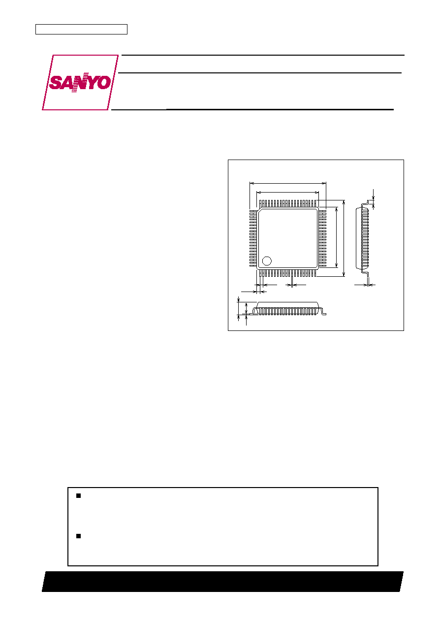
Package Dimensions
unit: mm
3255-QFP80
14.0
14.0
17.2
17.2
0.15
0.1
3.0max
0.25
0.65
(0.83)
(2.7)
0.8
1
20
21
40
41
60
80
61
[LA17000M]
SANYO: QFP80 (14 x 14)
Overview
The LA17000M is an all-in-one car tuner IC that incorpo-
rates a PLL frequency synthesizer and all functions of an
AM/FM tuner in a single chip. By combining two chips, a
PLL (LC72144 equivalent) and an FM tuner IC (LA1781M
equivalent) into a single chip (*PLL + AM (up conversion)
+ FMFE + IF + NC + MCP + MRC), and as a result of
optimal chip partitioning, the LA17000M improves the
performance of car tuner systems, eliminates adjustments,
and provides high reliability, all at a lower cost.
Features
∑ PLL on chip
∑ ADC (6 bits, 1 channel)
∑ IF counter and I/O port on chip permit simplification
of the interface.
∑ Supports AM double conversion.
∑ Enhanced noise countermeasures
∑ Excellent tri-signal characteristics
∑ Improved medium and weak electric field NC
characteristics
∑ Improved separation characteristics
∑ Anti-birdie filter on chip (analog/digital output)
∑ Multipath sensor output (analog/digital output)
∑ Cost-saving features
∑ AM double conversion (Up conversion method)
∑ Enhanced FM-IF circuit
(When there is interference from adjacent frequencies,
the software handles switching of the CF between
wide and narrow automatically.)
∑ Because deviations in IF gain are only 1/3 that of
earlier devices, adjustment is simplified when this IC
is incorporated into a set; this IC also includes a shifter
pin for VSM adjustment.
∑ Suited for smaller devices
∑ Permits high-frequency signal line processing in a
tuner pack.
∑ Easily conformes to FCC standards
LA17000M
No. 6522-2/54
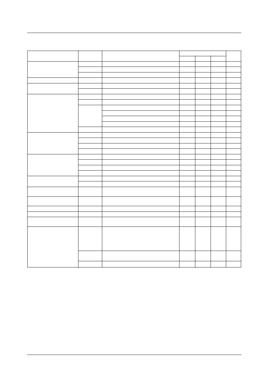
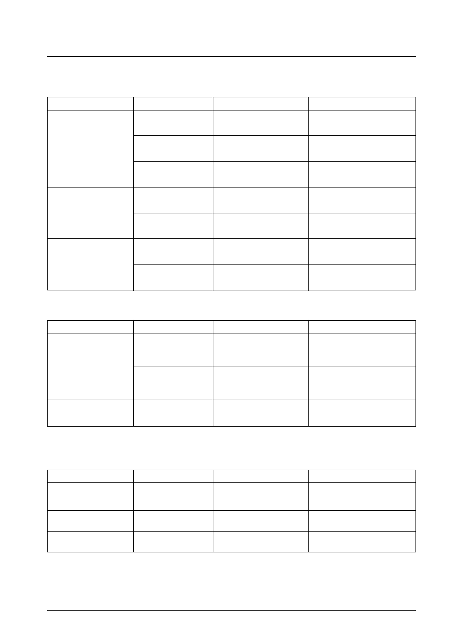
Maximum Ratings at Ta = 25∞C
Parameter
Symbol
Conditions
Ratings
Unit
Maximum supply voltage
V
CC
1 max
Pins 6, 56, and 77
8.7
V
V
CC
2 max
Pins 7, 61, 70, 75, and 76
12.0
V
V
DD
max
Pin 19
6.0
V
Allowable power dissipation
Pd max
Ta
85∞C, * With board
950
mW
Operating temperature
Topr
≠40 to +85
∞C
Storage temperature
Tstg
≠40 to 150
∞C
* Specified board: 114.3
◊ 76.1 ◊ 1.6 mm
3
, glass epoxy
Operating Conditions at Ta = 25∞C
Parameter
Symbol
Conditions
Ratings
Unit
Recommended supply voltage
V
CC
Pins 6, 7, 56, 61, 70, 75, 76, and 77
8.0
V
Pin 19
5.0
V
Operating supply voltage range
V
CC
op
7.5 to 8.5
V
V
DD
op
4.5 to 5.5
V
Tuner Block
Operating Characteristics at Ta = 25∞C, V
CC
= 8.0 V, V
DD
= 5.0 V, in the specified Test Circuit
Parameter
Symbol
Conditions
Ratings
min
typ
max
Unit
[FM characteristics] FM IF input
Current drain
I
CCO
-FM
No input, I56 + I61 + I70 + I75 + I76 + I79
60
98
110
mA
Demodulated output
220
330
445
mVrms
Channel balance
CB
≠1
0
+1
dB
Total harmonic distortion
THD-FMmono 10.7 MHz, 100 dB
µV, 1 kHz, 100% mod, pin 15
0.4
1
%
Signal-to-noise ratio IF
S/N-FM IF
10.7 MHz, 100 dB
µV, 1 kHz, 100% mod, pin 15
75
82
dB
AM suppression ratio IF
AMR IF
55
68
dB
Muting attenuation
Att-1
3
8
13
dB
Att-2
13
18
23
dB
Att-3
26
31
36
dB
Separation
Separation
25
35
dB
Stereo ON level
ST-ON
Pilot modulation at which V17 < 0.5 V
4.1
6.6
%
Stereo OFF level
ST-OFF
Pilot modulation at which V17 > 3.5 V
1.2
3.1
%
Main total harmonic distortion
THD-Main L
0.4
1.2
%
Pilot cancellation
PCAN
12
22
dB
SNC output attenuation
AttSNC
1
5
9
dB
HCC output attenuation
AttHCC-1
1
5
9
dB
AttHCC-2
6
10
14
dB
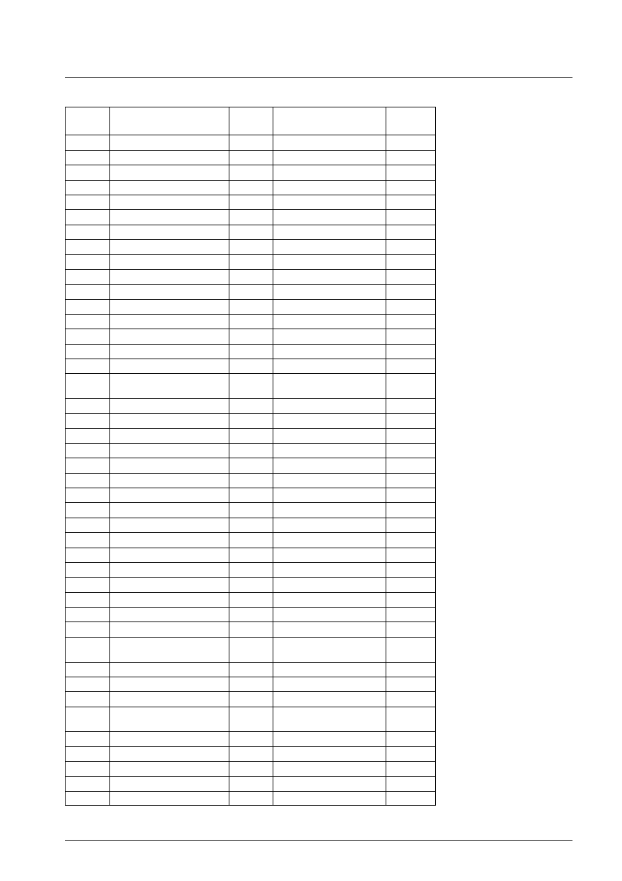
Continued on next page.
10.7 MHz, 100 dB
µV, 1 kHz, 100%mod,
pin 15 output
10.7 MHz, 100 dB
µV, 1 kHz,
ratio of pin15 and pin 16
10.7 MHz, 100 dB
µ, 1 kHz, fm = 1 kHz, pin 15
at 30% AM
10.7 MHz, 100 dB
µV, 1 kHz, attenuation on
pin 15 when V49 = 0
2 V
10.7 MHz, 100 dB
µV, 1 kHz, attenuation on
pin 15 when V49 = 0
2 V *Note 1
10.7 MHz, 100 dB
µV, 1 kHz, attenuation on
pin 15 when V49 = 0
2 V *Note 2
10.7 MHz, 100 dB
µ, L + R = 90%,
pilot = 10%, pin 15 output ratio
10.7 MHz, 100 dB
µV, L + R = 90%,
pilot = 10%, pin 15
10.7 MHz, 100 dB
µV, pilot = 10%,
pin 15 signal/PILOT-LEVEL leak DIN AUDIO
10.7 MHz, 100 dB
µV, L ≠ R = 90%,
pilot = 10%, V44 = 3 V
0.6 V, pin 15
10.7 MHz, 100 dB
µV, 10 kHz, L + R = 90%,
pilot = 10%, V45 = 3 V
0.6 V, pin 15
10.7 MHz, 100 dB
µV, 10 kHz, L + R = 90%,
pilot = 10%, V45 = 3 V
0.1 V, pin 15
LA17000M
No. 6522-3/54
Continued from preceding page.
Parameter
Symbol
Conditions
Ratings
min
typ
max
Unit
Input limiting voltage
V
IN
-LIM
29
36
dB
µ
V
Muting sensitivity
V
IN
-MUTE
IF input level non-mod when V49 = 2 V
19
27
35
dB
µ
V
SD sensitivity
SD-sen1 FM
48
56
64
dB
µ
V
SD-sen2 FM
48
56
64
dB
µ
V
IF counter buffer output
V
IFBUFF-FM
1
145
245
330
mVrms
V
IFBUFF-FM
2
145
245
330
mVrms
Signal meter output
V
SM
FM-1
No input, pin 42 DC output non-mod
0.0
0.1
0.3
V
V
SM
FM-2
50 dB
µ
, pin 42 DC output non-mod
0.65
1.6
2.4
V
V
SM
FM-3
70 dB
µ
, pin 42 DC output non-mod
2.4
3.2
4.2
V
V
SM
FM-4
100 dB
µ
, pin 42 DC output non-mod
4.9
5.8
6.5
V
Muting bandwidth
BW-MUTE
140
210
280
kHz
Muting drive output
V
MUTE
-100
100 dB
µ
V, 0 dB
µ
, pin 49 DC output non-mod
0.00
0.1
0.3
V
[FM FE Block]
N-AGC on input
V
NAGC
72
79
86
dB
µ
V
W-AGC on input
V
WAGC
90
97
104
dB
µ
V
Conversion gain
A. V1
83 MHz, 80 dB
µ
, non-mod, FECF output
9
13
17
dB
A. V2
13
17
21
dB
Oscillator buffer output
V
OSCBUFFFM
No input, pin 5 output
51
67
102
mVrms
[NC Block] NC input (pin 30)
Gate time
GATE
f = 1 kHz, 1
µ
s, 100 mVp-o pulse input
15
µ
s
Noise sensitivity
SN
18
mVp-o
[MRC Block]
MRC output
V
MRC
V42 = 5 V
2.1
2.25
2.4
V
MRC operating level
MRC-ON
22
33
44
mVrms
MRC sensor output
V
MRC
-sensor1 V42 = 5 V, pin 34 output
1.5
1.9
V
V
MRC-
sensor2
V42 = 5 V, pin 48 output, f = 70 kHz, 100 mVrms
2.1
2.9
V
[AM Characteristics] AM ANT input
Practical sensitivity
S/N-30
1 MHz, 30 dB
µ
V, fm = 1 kHz, 30% mod, pin 15
15
dB
Detection output
V
O
-AM
1 MHz, 74 dB
µ
V, fm = 1 kHz, 30% mod, pin 15
105
160
220
mVrms
AGC-F.O.M
V
AGC-FOM
50
55
60
mVrms
Signal-to-noise ratio
S/N-AM
1 MHz, 74 dB
µ
V, fm = 1 kHz, 30% mod
47
52
dB
Total harmonic distortion
THD-AM
1 MHz, 74 dB
µ
V, fm = 1 kHz, 80% mod
0.5
1.2
%
Signal meter output
V
SM
AM-1
1 MHz, 30 dB
µ
V, non - mod
0.6
1
1.4
V
V
SM
AM-2
1 MHz, 120 dB
µ
V, non - mod
3.4
4.5
5.9
V
Oscillator buffer output
V
OSCBUFF
AM-1 No input, pin 5 output
170
210
mVrms
Wideband AGC sensitivity
W-AGCsen1
1.4 MHz, input when V62 = 0.7 V
87
93
99
dB
µ
V
W-AGCsen2
1.4 MHz, input when V62 = 0.7 V (during SEEK)
78
84
90
dB
µ
V
Continued on next page.
10.7 MHz, 100 dB
µ
V, 30% mod, IF input that
decreases the input reference output by ≠3 dB
IF input non-mod (at least 100 mVrms) at
which the IF count buffer output turns on
10.7 MHz, 100 dB
µ
V, non-mod, pin 38 output,
during SEEK
83 MHz, 80 dB
µ
, non-mod, 5 V applied to CF
(pin 10), FECF output
1 kHz, 1
µ
s pulse input that starts noise
canceller operation. Measured at Pin 30.
Input level on pin 48 that is below
pin 42 = 5 V and pin 43 = 2 V, f = 70 kHz
1 MHz, 74 dB
µ
V, output reference, input width
at which output drops by 10 dB, pin 15
10.7 MHz, 100 dB
µ
V, non-mod,
pin 38 output, during RDS mode
100 dB
µ
V, when V49 = 2 V
Bandwidth non-mod
83 MHz, non-mod, input at which pin 2 is
2.0 V or less
83 MHz, non-mod, input at which pin 2 is
2.0 V or less (when KEYED-AGC is 4.0 V)
LA17000M
No. 6522-4/54
Continued from preceding page.
Parameter
Symbol
Conditions
Ratings
min
typ
max
Unit
SD sensitivity
SD-sen1AM
27
33
39
dB
µ
V
SD-sen2AM
1 MHz, ANT input level at which SD pin turns on
27
33
39
dB
µ
V
IF buffer output
V
IFBUFF-AM
1 MHz, 74 dB
µ
V, non-mod, pin 38 output
150
220
mVrms
PLL Block
Allowable Operating Ranges
at Ta = ≠40 to +85∞C, V
DD
= 5 V, V
SS
= 0 V
Parameter
Symbol
Conditions
Ratings
min
typ
max
Unit
High-level input voltage
V
IH
1
CE, CL, DI, I/O-1, I/O-2
2.2
V
DD
+ 0.3
V
Low-level Input voltage
V
IL
1
CE, CL, DI, I/O-1, I/O-2, SDSTSW
0
0.8
V
Output voltage
V
O
1
DO
0
6.5
V
V
O
2
I/O-1, I/O-2
0
13
V
Input amplitude
f
IN
1
X
IN
; Sine wave, capacitor coupled
1
8
MHz
f
IN
2
PLL
IN
; Sine wave, capacitor coupled
10
160
MHz
f
IN
3
HCTR; Sine wave, capacitor coupled
0.4
25
MHz
X'tal
10.1
10.5
MHz
Input amplitude
V
IN
1
X
IN
200
1500
mVrms
V
IN
2-1
PLL
IN
;
10
f < 130 MHz; Note 2
40
1500
mVrms
V
IN
2-2
PLL
IN
; 130
f <160 MHz; Note 2
70
1500
mVrms
V
IN
3-1
40
1500
mVrms
V
IN
3-2
70
1500
mVrms
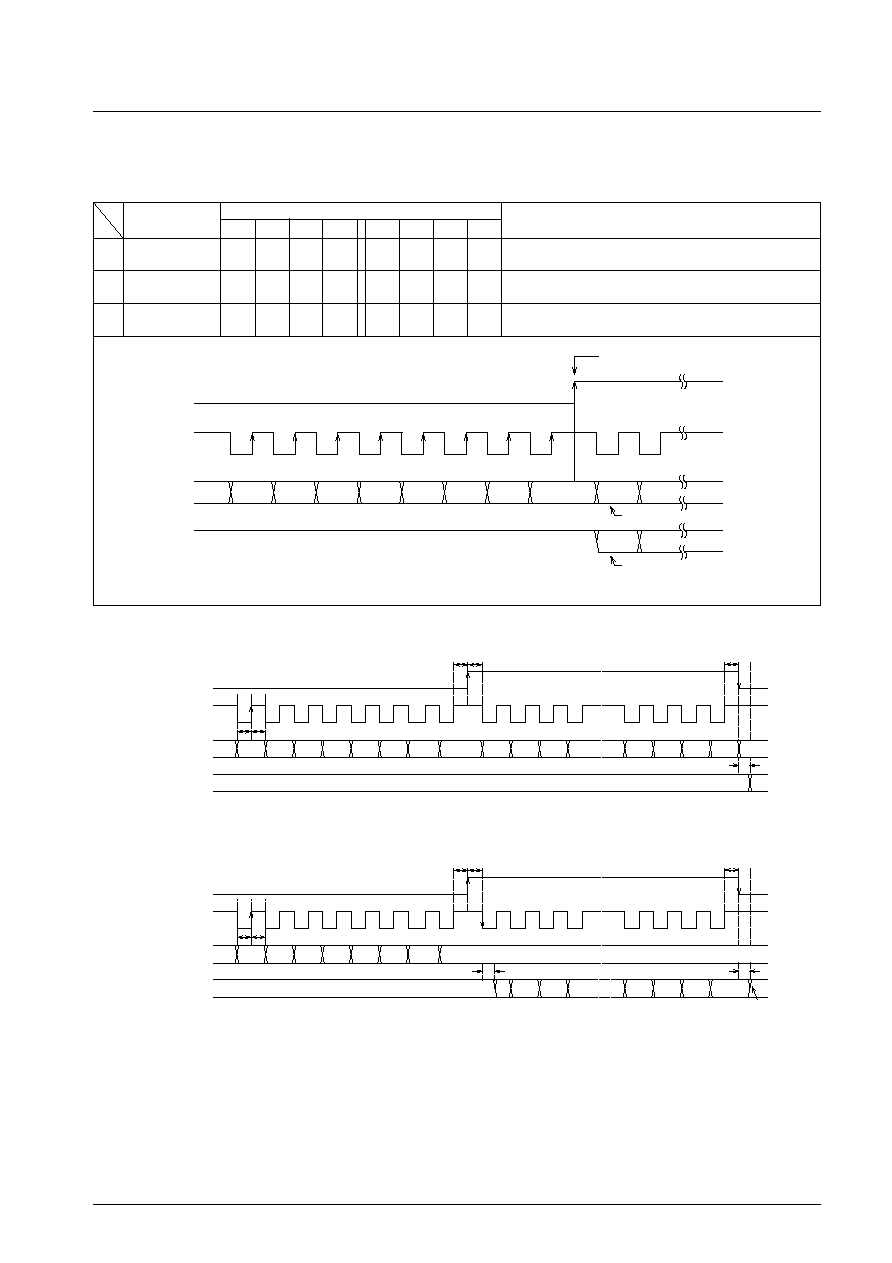
Data setup time
t
SU
DI, CL: Note 5
0.45
µ
s
Data hold time
t
HD
DI, CL: Note 5
0.45
µ
s
Clock low-level time
t
CL
CL: Note 5
0.45
µ
s
Clock high-level time
t
CH
CL: Note 5
0.45
µ
s
CE wait time
t
EL
CE, CL: Note 5
0.45
µ
s
CE setup time
t
ES
CE, CL: Note 5
0.45
µ
s
CE hold time
t
EH
CE, CL: Note 5
0.45
µ
s
Data latch change time
t
LC
Note 5
0.45
µ
s
Data output time
t
DC
0.2
µ
s
t
DH
0.2
µ
s
Note 1:
Recommended CI value for crystal oscillator
CI
70
(X'tal: 10.25, 10.35 MHz)
However, because the characteristics of the X'tal oscillation circuit depend on the board and circuit constants,
we recommend requesting that the X'tal manufacturer perform the evaluation.
Note 2:
Refer to the program divider configuration.
Note 3:
Serial data: CTC = 0
Note 4:
Serial data: CTC = 1
Note 5:
Refer to the serial data timing.
Guaranteed crystal oscillator
ranges
X
IN
, X
OUT
; CI
70
(X'tal: 10.25, 10.35 MHz); Note 1
HCTR; 0.4
f < 25 MHz: Serial data;
CTC = 0: Note 3
HCTR; 8
f <12MHz: Serial data;
CTC = 1: Note 4
DO, CL; Dependent on pull-up resistance,
board capacity: Note 5
DO, CL; Dependent on pull-up resistance,
board capacity: Note 5
1 MHz, ANT input level at which IF count
output turns on
LA17000M
No. 6522-5/54
PLL Characteristics
Electrical Characteristics
at Ta = 25∞C, V
DD
= 5 V, V
SS
= 0 V
Parameter
Symbol
Conditions
Ratings
min
typ
max
Unit
Built-in feedback resistors
Rf1
X
IN
1
M
Rf2
PLL
IN
500
k
Rf3
HCTR
250
k
Hysterisis width
V
HIS
CE, CL, DI
0.1V
DD
V
High-level output voltage
V
OH
1
PD1, PDS, SEEKSW; I
O
= ≠1 mA
V
DD
≠1.0
V
V
OH
2
XBUF; I
O
= ≠0.5 mA
V
DD
≠1.5
V
Low-level output voltage
V
OL
1
PD1, PDS, SEEKSW; I
O
= ≠1 mA
1
V
V
OL
2
XBUFF; I
O
= ≠0.5 mA
1.5
V
V
OL
3
I/O-1 to I/O-2; I
O
= 1.0 mA
0.2
V
I/O-1 to I/O-2; I
O
= 2.5 mA
0.5
V
I/O-1 to I/O-2; I
O
= 5.0 mA
1
V
I/O-1 to I/O-2; I
O
= 9.0 mA
1.8
V
V
OL
4
DO; I
O
= 5.0 mA
1
V
High-level input current
I
IH
1
CE, CL, DI; V
IN
= 6.5 V
5
µ
A
I
IH
2
I/O-1 to I/O-2; V
IN
= 13 V
5
µ
A
I
IH
3
X
IN
; V
IN
= V
DD
2
11
µ
A
I
IH
4
PLL
IN
; V
IN
= V
DD
4
22
µ
A
Low-level input current
I
IL
1
CE, CL, DI; V
IN
= 0 V
5
µ
A
I
IL
2
I/O-1 to I/O-2; V
IN
= 0 V
5
µ
A
I
IL
3
X
IN
; V
IN
= 0 V
2
11
µ
A
I
IL
4
PLL
IN
; V
IN
= 0 V
4
22
µ
A
Output off leakage current
I
OFF
1
I/O-1 to I/O-2; V
O
= 13 V
5
µ
A
I
OFF
2
DO; V
O
= 6.5 V
5
µ
A
I
OFFH
PD1, PDS; V
IN
= V
DD
0.01
200
nA
I
OFFL
PD1, PDS; V
IN
= 0 V
0.01
200
nA
Input capacitance
C
IN
6
pF
A/D converter linearity error
Err
MRC SENSOR AUTO ADJ (MOS)
≠0.5
+0.5
LSB
Rpd1
PLL
IN
80
200
600
k
Supply current
I
DD
1
10
15
mA
I
DD
2
5
10
mA
I
DD
3
V
DD
; PLL block halt, X'tal OSC halt
3
mA
High-level 3-state off leakage
current
Low-level 3-state off leakage
current
Pull-down transistor on
resistance
V
DD
; X'tal = 10.25 MHz,
f
IN
2 = 160 MHz,
V
IN
2 = 70 mVrms,
f
IN
3 = 25 MHz,
V
IN
3 = 40 mVrms
V
DD
; PLL block halt (PLL INHIBIT),
X'tal OSC operation (10.25 MHz)
LA17000M
FM RF AGC
FE GND
FMOSC
OSC BUFFER
AM/FM
AM OSC
NC Sens
NC AGC
XBUFF IN
Gore OUT
LPF OUT
MPX Pdot IN
NC MPX GND
Lch OUT
Rch out
SDSTSW
PLL IN
PLL V
DD
FM MIX IN
FM ANTD
1
2
3
4
5
0.022
µ
F
16V/100
µ
F
0.022
µ
F
0.022
µ
F
0.022
µ
F
8pF
k
k
10.7Hz
10.7MHz
450kHz
1000pF
100
µ
H
FC18
2.2
µ
H
16V/47
µ
F
0.022
µ
F
0.022
µ
F
16V/47
µ
F
0.01
µ
F
0.01
µ
F
0.01
µ
F
0.022
µ
F
82pF
8
2pF
68pF
0.022
µ
F
0.022
µ
F
3.3
µ
F
0.1
µ
F
100
µ
H
0.022
µ
F
33mH
100
µ
H
65pF
6pF
15pF
1SV234
1SV234
0.022
µ
F
30
3
7
4
6
2
k
6
7
8
9
10
11
12
13
14
15
16
17
18
19
AM/FM S-METER
42
MRC OUT
43
SNC
44
HCC
45
NC IN
46
DET OUT
47
FM S-METER MRC IN
48
MUTE
49
AFC IN
50
QD OUT
51
QD IN
52
V
REF
53
FM SD
54
KEYED AGC
55
V
CC
56
C-HCC
57
AM LC
58
PILOT DET
59
IF AGC
60
41
PD1
20
PLL VSS
21
PDS
22
XBUFF
23
I/O2
24
X IN
25
X OUT
26
CE
27
CI
28
CL
29
DO
30
I/O1
31
HCTR
32
SEEKSW
33
MRC SENSOR OUT ADC 0
34
PC IN
35
PC OUT
36
MPX VCO
37
IF COUNT BUFF SEEK/STOP SELECT
38
GND
39
40
80
AM 1st MIX IN
79
1st IF IN (NARROW)
78
FE VCC
77
MIX OUT
76
MIX OUT
75
NARROW AGC IN/MUTE ATT ADJ
74
AM RF AGC OUT
73
1st IF (WIDE)
72
AM SD ADJ/WIDE AGC IN
71
AM MIX OUT
70
1st IF OUT
69
AM IF IN
68
FM IF IN
67
FM IF BYPASS
66
2nd MIX IN
65
RF AGC
64
FM MUTE ADJ
63
AM ANTD/WIDE AGC
AM FT
62
61
LA17000M
+
+
+
+
+
+
+
+5V
--5V
--
+
0.022
µ
F
0.01
µ
F
CC
270pF
30pF
100pF
1M
NC
U
30k
0.47
µ
F
0.015
µ
F
100pF
0.01
µ
F
0.1
µ
F
0.01
µ
F
1000pF
1
µ
F
1
2
3
4
9
8
7
6
712-12
1025MHz
0.01
µ
F
1
µ
F
180pF
112NME
112LDA
0.1
µ
F
1
µ
F
1
µ
F1
µ
F
0.047
µ
F
1
µ
F
0.22
µ
F
0.022
µ
F
912kHz
16V/10
µ
F
16V/1
µ
F
16V/100
µ
F
16V/1
µ
F
0.022
µ
F
0.01
µ
F
0.22
µ
F
0.22
µ
F
22
µ
F
1
µ
F
3.3
µ
F
0.022
µ
F
10.7Hz
10.7Hz
51k
10k
50
51k
350
CR
50
10k
10k
SOFP80
10k
2SK583
1M
50
10k
47k
200
22pF
22pF
47k
47k
33k
5.6k
PHASE COMP
50
1k
330
47k
15k
1M
100k
P1
100k
10k
100k
100k
43k
10k
30k
20k
10k
10k
SIGNAL
-MATER
-Z
SEP
-VOL
-L
SEP
-VOL
-H
SW11
NC
-IN
-GND
NC
-IN
DET
-OUT
MRC
-IN
MUTE
SW12
DET
-ADJ
SYS-PS+15V
SYS-PS-GND
SYS-PS---15V
DZ1
SYS-PS+12V
CENTER-MATER
AM-STREO-OUT
AM-STREO-OUT-GND
1st-IF-OUT
SW13
SW14
FM-IF-INPUT
SW40
SW41
RF-MIX-VCC
RF-MIX-VCC-G
AM-VCC
AM-ANT-INPUT
AM-ANT-DUMP
FM-ANT-INPUT
SW01
FM-ANT-DUMP
FM-AGC
FM-MIX-INPUT
10k
6.8k
10k
100
k
10k
240k
L78MO5T
I
G
O
82pF
82pF
8200pF
750pF
82pF
SVC203
VR
P1
2.2k
D
G
S
150pF
6800pF
112LDA
112LDA
1M
30pF
P1
0.015
µ
F
P1
+
16V/100
µ
F
0.01
µ
F
FM
-V
CC
SW18
OSC
-BUFF
-OUT
NC
-HPF
-OUT
SW02
CF SW
SW03
SW04
SW05
GATE
-OUT
L -
CH
-OUT
NC
-LPF
-OUT
R
-CH
-OUT
ST
-SD
SW06
VF/IMZ
-G
VF/IMZ
-S
VF/IMZ
-F
PLL -VCC
VT-OUT
2nd-OSC-BUFF
IOZ
SW17
X-IN
DUT-CCB-CE
DUT-CCB-CL
DUT-CCB-DI
DO
IO1
SW16
IF-COUNT-IN
IF-COUNT-BUFF
MRC-SENSOR-OUT
SW07
MPX-FREO
SIGNAL-MATER-1
MRC-OUT
SW08
SW09
VDDSNC/HCC1
5V
FMIF AM NC MPX V
CC
PLL
-IN
CC
3
U
7
4
6
2
+
+5V
--5V
--
0.01
µ
F
CC
0.01
µ
F
CC
CR
+12V
NC
3
7
6
5
1
2
+
+15V
--
NC
NC
0.1
µ
F
3
7
5
1
4
6
2
+
+15V
--15V
--15V
--
0.1
µ
F
0.01
µ
F
NC
NC
0.1
µ
F
3
7
8
1
4
5
6
2
+
--15V
+15V
+15V
+15V
+5V
--5V
--15V
+12V
--
0.1
µ
F
NC
NC
0.1
µ
F
3
7
5
1
4
6
2
+
--15V
--15V
--
0.1
µ
F
NC
NC
0.1
µ
F
0.01
µ
F
50
1M
+5V
3
7
4
6
2
+
--5V
--
0.01
µ
F
0.01
µ
F
0.022
µ
F
0.022
µ
F
50
330
4
0.1
µ
F
PLL VCC
D
C
B
S
E
G
0.022
µ
F
1M
50
3
U
7
4
6
2
+
+5V
--5V
--
0.01
µ
F
CC
0.01
µ
F
CC
CR
50
50
1M
CR
50
3
U
7
4
6
2
+
+5V
--5V
--
0.01
µ
F
CC
0.01
µ
F
CC
CR
5pF
10pF
18pF
100pF
30
150
30
200k
30k
510
100
30k
200k
3SK263
30k
150
560
33
100k
100k
0.01
µ
F
2200pF
180pF
180k
100k
50
25
30
10pF
15pF
18k
1SV234
1SV234
1000pF
16V/100
µ
F
+
15pF
1000pF
50
16V/47
µ
F
0.01
µ
F
+
L79MO5T
I
G
O
A13289
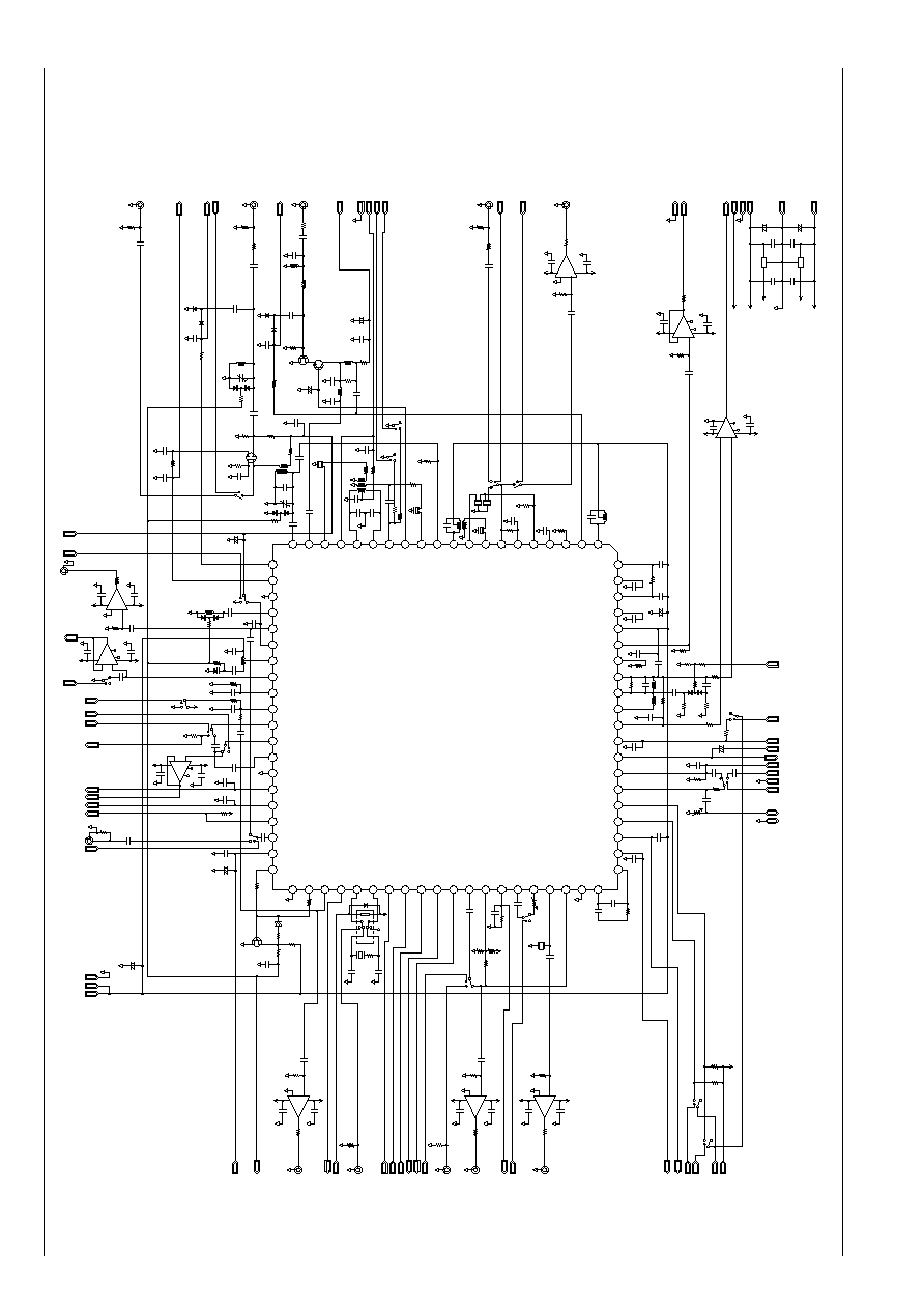
Test Circuit
No. 6522-6/54

LA17000M
No. 6522-7/54
[FM IF Selectivity Switching Circuit]
Features
1) Comprises an FM/AM one-chip system.
2) Up conversion method is adopted for AM.
3) Uses an IF filter with a center frequency that is the same as the middle frequency of FM.
4) Uses a narrowband filter in AM mode.
5) Uses a narrowband filter in FM mode only during SEEK or when there is interference from adjacent frequencies.
6) Uses a wideband filter for normal reception in FM mode.
7) For an RDS AF search, switches to a narrowband filter and detects SD.
8) High sensitivity for detecting interference from adjacent frequencies.
Advantages
1) This FM/AM one-chip tuner system (an IC that includes a microcontroller interface) allows for improved adjacent
frequency interference characteristics without increased cost.
2) Prevents SD and IF count misdetection (station detection) during seek search, RDS AF search, and auto memory
operations.
3) Permits adoption of an IC for certain functions without increasing the number of IC pins.
4) CF selectivity can be switched by the software in the microcontroller that controls the tuner, making it easy to
achieve performance differentiation through the software.
(The software can freely set the CF switching timing and conditions.)
5) Detects the radio wave status in the field through detection of SD, desired station field intensity, IF count output, and
adjacent station field intensity. This IC offers improved adjacent frequency interference characteristics by switching
the CF automatically when interference is being generated from an adjacent frequency.
[IF Band Switching Circuit]
Purpose
This AM/FM one-chip tuner IC automatically switches the FM selectivity, prevents misdetection during SEEK opera-
tions, and offers improved adjacent frequency interference characteristics without any increase in cost.
New Technological Features
1.
Comprises an AM/FM one-chip IC.
2.
Because the narrowband CF that is used by the AM UP conversion system is also used for FM, additional external
components required by earlier systems can be eliminated.
3.
Uses a wideband CF during normal FM reception for high sound quality.
4.
Uses a narrowband CF for AM reception, and if interference is being generated from adjacent frequencies during
FM reception.
5.
Uses a narrowband CF during SEEK and RDSAF search operations, preventing misdetection of SD and IF count
due to adjacent stations.
6.
CF switching is performed at the first IF amp input, and the amp gain is adjusted automatically to a suitable level
according to the CF band form AM/FM or FM.
7.
Switching of the CF input and the first IF amp gain is controlled by a microcontroller through the interface. The
pins that are controlled are connected to the I/O ports of the microcontroller, and are controlled by the
microcontroller's internal software.
8.
Detection of adjacent frequency interference during FM reception is based on S-meter output, SD, and IF count
output. The IF count buffer frequency fluctuates when interference is being generated from adjacent frequencies.
This fluctuation is used to make the detection of interference from adjacent frequencies possible. (Related patents
have been applied for.)
Conventional Technologies
1.
Comprised of a dedicated IC for IF band switching, or of multiple ICs.
2.
None of the AM/FM all-in-one chip systems include the functions provided by the LA17000M.
3.
Requires a narrowband CF especially for FM, resulting in increased costs. (Does not share the AM narrowband CF.)
4.
Because CF switching control is handled by analog circuits or logic circuits, the switching timing can only be
controlled through uniform conditions. Control by software is not possible.
LA17000M
No. 6522-8/54
VCC
LO
SL
A13290
10.7
Fd
FdL
FdH
f (MHz)
A13291
10.7
Fd
Fud
f (MHz)
A13292
A13293
Fd
FdL
FdH
A13294
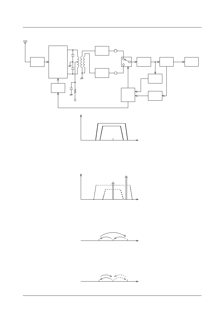
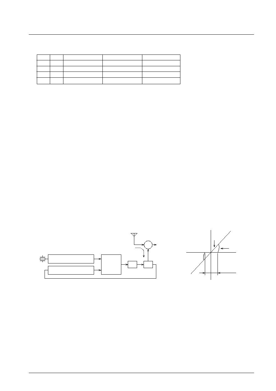
Conceptual Diagram of the FM-IF Band Switching System
Mixing
FM
RF
FM
DET
Local
oscillation
Wideband
filter
Narrowband
filter
Control
circuit
Wideband
filter
Limiter
amp
IF
counter
Field
intensity
Level
A
B
C
D
Wideband
Narrowband
LA17000M
No. 6522-9/54
I/O Port Assignment Table
I/O-0
DI data
I/O-1
I/O-2
DI data
I/O-3
DO data
OUTPUT
PLL output port
INPUT
PLL input port
OUTPUT
PLL output port
INPUT
I/O-3 = 0 (input port)
OUT3 = 1 (OPEN or high)
PLL input port
Cannot be set as output port
L: Reception mode
H: Seek mode
OPEN: RDS
Unused
H: Dx mode
L: Lo mode
When reception mode is set
H: Monaural
L: Stereo
When seek mode is set
H: SD ON
L: SD OFF
The MRC sensor reads DO data from the PLL microcontroller's 6-bit A/D converter.
Currently, aside from the CCB data lines, only three lines are connected to the controller microcontroller: CF/SW,
AUDIO mute, and AM/FM band switching port.
Selectivity Switching Evaluation Software State-based Data Switching Table
Tuner processing
Seek
Manual preset
Receiving
Remarks
I/O port state
CF switching
WIDE
NARROW
AUDIO mute output
ON
Switchable but fixed by software
OFF
Switchable but fixed by software
Lo/Dx
Lo
Processing is performed according
to the setting
Dx
Processing is performed according
to the setting
Mode switching
Seek mode
I/O-3 is SD output
Reception mode
I/O-3 is monaural/stereo output
RDS mode
I/O-3 is SD output
IF count
Output ON
Seek mode
RDS mode
Output OFF
Reception mode
LA17000M
No. 6522-10/54
Additional Settings (Added to the LC72144M)
Output (DI)
Mode
Settings
When set
Seek mode
For seek
Tuner mode switch
Reception mode
For seek-stop and for receiving
RDS mode
For AF search
Lo mode
When setting Lo mode
Lo/Dx switch
Dx mode
When setting Dx mode
Mute ON
For tuning processing
Hard mute *1
Mute OFF
When switching reception mode
DI data IN2
I/O-0 = 1 (output port)
OUT0 = 1 (Hi)
DI data IN2
I/O-0 = 1 (output port)
OUT0 = 0 (Lo)
DI data IN2
I/O-0 = 0 (input port)
OUT0 = 1 (OPEN)
DI data IN2
I/O-2 = 0 (output port)
OUT2 = 0 (Lo)
DI data IN2
I/O-2 = 1 (output port)
OUT2 = 1 (Hi)
DI data IN2
I/O-0 = 1 (output port)
OUT1 = 1 (Hi)
DI data IN2
I/O-0 = 1 (output port)
OUT1 = 1 (Lo)
Note: *1. Depends on the I/O ports usage.
Input (DO)
DO data
Conditions
When the tuner mode is set to
reception mode
*2
Sensor
When the tuner mode is set to seek or
RDS mode
*2
MRC output
Start AD conversion and then read
after conversion is completed.
3.3 V at 6-bit resolution
OUT data I3 = 1 (Hi)
Monaural state
OUT data I3 = 0 (Lo)
Stereo state
OUT data I3 = 1 (Hi)
SD ON
OUT data I3 = 0 (Lo)
SD OFF
OUT data ADC0
AD00 to AD05
6 bit
Monaural/stereo
SD
Note: *2. I/O-3 = 0 (input port) and OUT3 = 1 (Hi) must already be set in the DI data (IN2) settings.
Other settings
In the LA17000
Setting
When set
For normal operation
CF switch
Pin 10
When there is interference from
adjacent frequencies
Soft mute (AUDIO mute)
Pin 49
Hi: Forced mute
When setting mute
Lo: Mute off
When cancelling mute
AM/FM switch
Pin 6
Lo: AM
For AM reception
Hi: FM
For FM reception
Hi: Wide (wideband setting)
Lo: Narrow (narrowband
setting)
LA17000M
No. 6522-11/54
Correspondence of Pins Between the LA17000M, the LA1781M, and the LC72144M
LA1781
Pin Function
LA17000M
Pin Function
LC72144M
Pin No.
Pin No.
Pin No.
1
FN ANTD
1
2
FM RF AGC
2
3
FE GND
3
4
FM OSC
4
5
AM/FM OSC buff.
5
6
FE V
CC
6
7
AM V
CC
7
8
Noise AGC-Sense
8
9
Noise AGC-ADJ
9
10
AM 2nd OSC
10
11
Gate Out
11
12
Memory circuit pin
12
13
Pilot In
13
14
NC, MPX GND
14
15
MPX L-Out
15
16
MPX R-Out
16
26
Seek
AM/FM SD
17
Both I/O-3 and SD/ST-IND
23
Stop
FM ST IND
18
FMIN
16
19
V
DD
17
20
PD1
18
21
V
SS
19
22
PDS
20
23
XBUF
22
24
I/O-2
8
25
XIN
24
26
XOUT
1
27
CE
2
28
DI
3
29
CL
4
30
DO
5
31
I/O-1
9
32
HCTR/I-6
11
33
I/O-0
12
19
MRC sensor output
34
7
17
Pilot Can. ADJ
35
18
Pilot Can. ADJ
36
20
MPX VCO
37
23
38
25
GND
39
21
PHASE COMP.
40
22
PHASE COMP.
41
24
AM/FM S-meter
42
27
MRC OUT
43
Continued on next page.
Both ADC0 and MRC
sensor output
IF count buffer and
seek/stop switch
LA17000M
No. 6522-12/54
Continued from preceding page.
LA1781
Pin Function
LA17000M
Pin Function
LC72144M
Pin No.
Pin No.
Pin No.
28
SNC control input
44
29
HCC control input
45
30
Noise canceller IN
46
31
AM/FM detector output
47
32
FM S-meter output
48
33
MUTE drive
49
34
AFC IN
50
35
QD OUT
51
36
CD IN
52
37
VREF
53
38
FMSD
54
39
GND Keyed AGC
55
40
V
CC
56
41
HCC capacitor
57
42
AM L.C.
58
43
Pilot detector
59
44
IF AGC
60
45
AM IFT (IF output)
61
46
AM ANTD
62
W-AGC IN
47
FM Mute ON ADJ
63
48
RF AGC
64
49
AM 2nd MIX IN
65
50
FM IF BYPASS
66
51
FM IF IN
67
52
AM IF IN
68
53
1st IF amplifier output
69
54
AM MIX OUT
70
55
W-AGC IN
71
AM SD ADJ
56
1st IF IN
72
57
AM RF AGC OUT
73
58
N-AGC IN
74
59
1st MIX OUT
75
60
1st MIX OUT
76
61
F.E.V
CC
77
64
FM MIX IN
78
1st IF narrow IN
62
AM MIX IN
79
63
FM MIX IN
80

LA17000M
No. 6522-13/54
PLL Block Functions
∑ High-speed programmable divider
∑ FMIN
: 10 to 160 MHz .......................... Pulse swallower method
∑ General-purpose counter
∑ HCTR
: 0.4 to 25.0 MHz ........................ Frequency measurement
∑ Crystal oscillator
: Two frequencies selectable: 10.35/10.25 MHz
∑ Reference frequencies : 12 frequencies selectable:
50, 30, 25, 12.5, 6.25, 3.125, 10, 9, 3, 5, and 1kHz
*1 *1 *1
*1: Not available when using the 10.25 MHz crystal oscillator
∑ Phase comparator
∑ Dead zone can be controlled
∑ Unlock detection circuit
∑ Sub-charge pump for high-speed locking
∑ Deadlock clear circuit on chip
∑ A/D converter ................................ 6 bits: 1 input (linked directly to MRC sensor output)
∑ Serial data I/O
Communications with controller possible in CCB format
∑ Power-on reset circuit
∑ On-chip crystal oscillator output buffer
∑ 2nd IF injection signal for AM up conversion (10.35/10.25 MHz)
∑ I/O port .......................................... General-purpose I/O: four ports
LA17000M
No. 6522-14/54
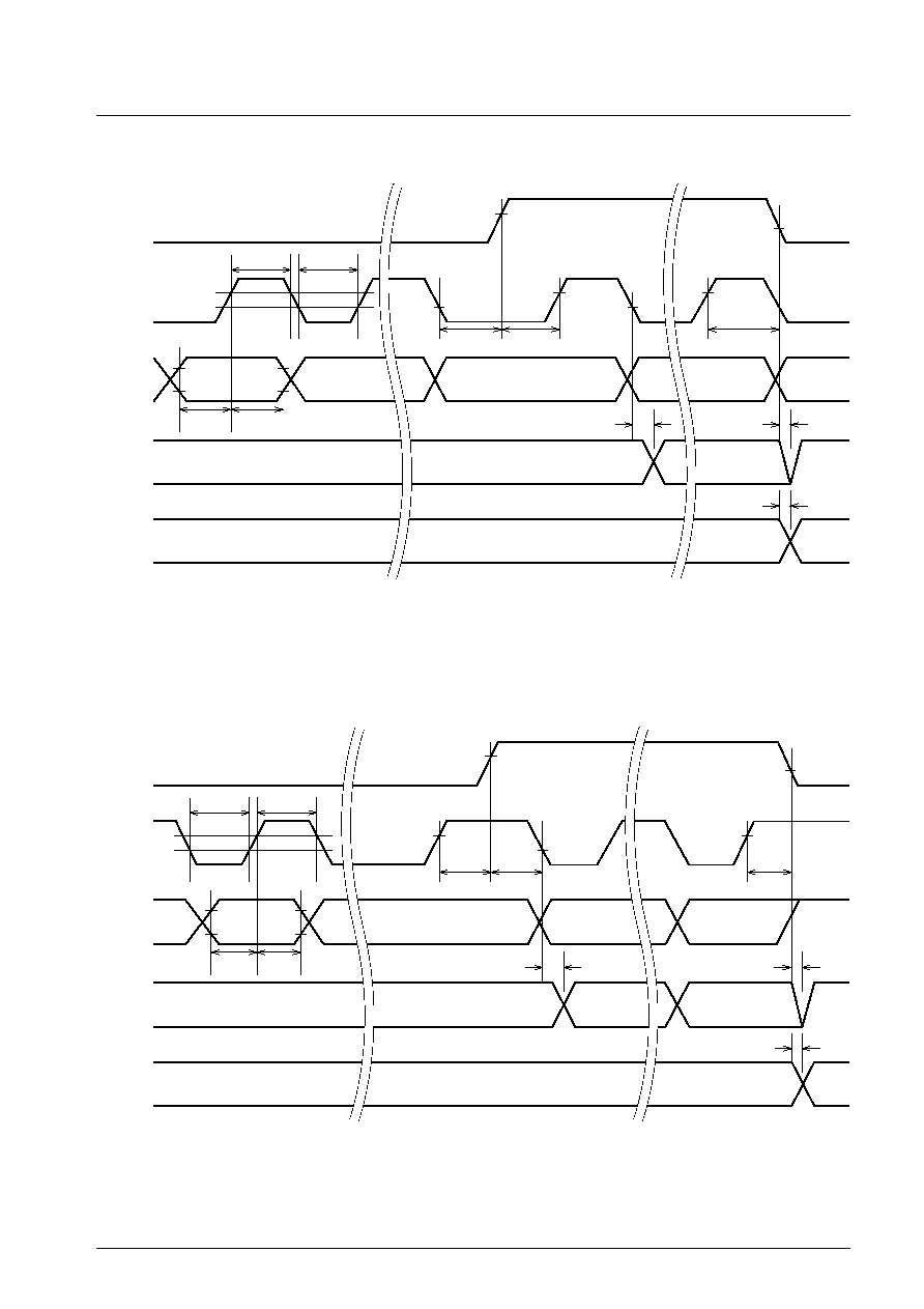
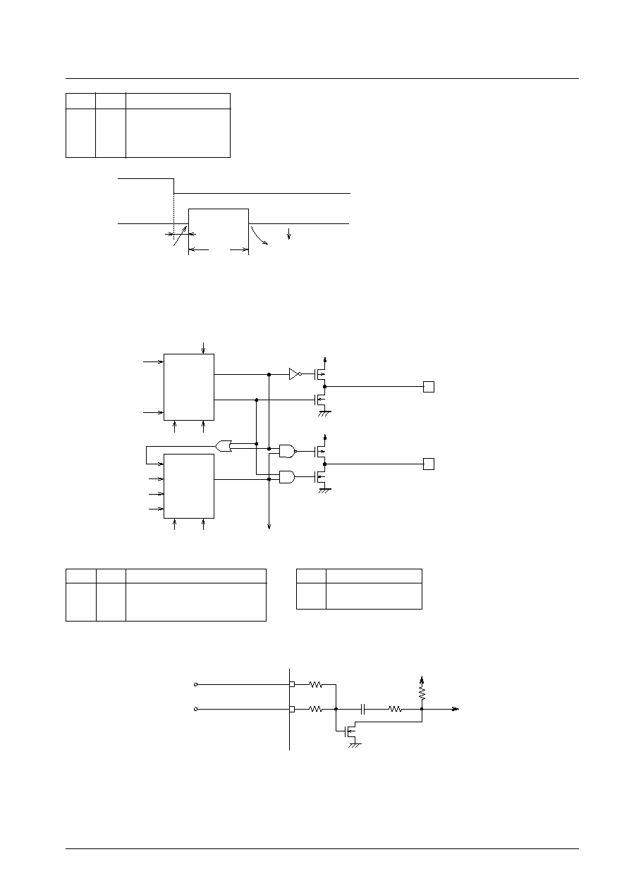
Serial Data Timing
tCH
tSU
tHD
VIH
VIH
VIH
VIL
VIH
VIL
VIL
VIH
VIL
VIH
VIL
VIL
tCL
tEL
tES
tEH
tDC
tDH
tLC
DI
CL
DO
CE
A13295
A13296
tCL
tSU tHD
VIH
VIH
VIH
VIL
VIH
VIL
VIL
VIH
VIL
VIH
VIL
tCH
tEL
tES
tEH
tDC
tDH
tLC
DI
CL
DO
CE
Internal
data latch
Internal
data latch
Old
New
Old
New
When CL is Stopped at the low level
When CL is Stopped at the high level

LA17000M
No. 6522-15/54
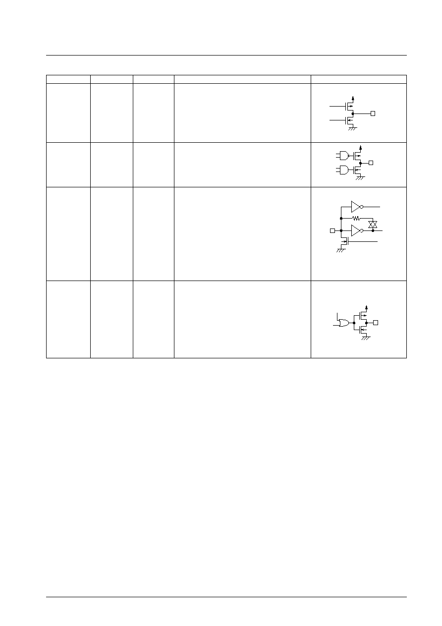
PLL Block Pin Description
Symbol
Pin No.
Description
Function
Pin Circuit
XIN
25
X'tal OSC
XOUT
26
PLL IN
18
CE
27
Chip enable
CL
29
Clock
DI
28
Input data
DO
30
Output data
V
DD
19
Power supply
V
SS
21
Ground
∑ This is the PLL ground pin.
I/O-1
31
I/O-2
24
STSD SW
17
SEEK SW
33
ADC0
34
ADC input
Continued on next page.
A13297
A13298
A13302
A13303
A13299
A13300
A13301
A13304
Local
oscillator
signal input
∑ For connecting the crystal oscillator.
(10.35, 10.25, 7.2 or 4.5 MHz)
∑ FMIN is selected when DVS in the serial data
input is set to 1.
∑ The input frequency range is from 10 to
160 MHz.
∑ The signal is transmitted to the swallow
counter.
∑ The divisor can be set to a value in the range
272 to 65535.
∑ This pin is set high during serial data input to
the PLL (DI) or during serial data output (DO).
∑ This pin is the clock for data synchronization
during serial data input to the PLL (DI) or
during serial data output (DO).
∑ This is the input pin for serial data that is
transferred from the controller to the PLL.
∑ This is the output pin for serial data that is
transferred from the controller to the PLL.
∑ This is the PLL power supply pin. Supply 4.5 V
to 5.5 V to this pin when the PLL is operating.
∑ When power is first applied to this pin, the
power-on reset circuit operates.
∑ These are general-purpose I/O ports.
∑ The output circuits open-drain.
∑ During a power-on reset, I/O-1 and I/O-2
become input ports. STSD SW becomes an
output port, and is fixed low.
∑ These ports can be switched between input
and output according to the serial data that is
transferred from the controller (I/O-1, I/O-2,
STSD SW).
∑ This is a general-purpose I/O port.
∑ The output circuits are complementary
circuits.
∑ During a power-on reset, this port becomes
an input port.
∑ This port can be specified as an input or
output port by the serial data that is trans-
ferred from the controller.
∑ This is the A/D converter input pin.
The converter is a 6-bit successive-approxi-
mation A/D converter.
For details, refer to the page that describes
the A/D converter configuration.
General-
purpose
I/O ports
General-
purpose
I/O port
A13305
LA17000M
No. 6522-16/54
Continued from preceding page.
Symbol
Pin No.
Description
Function
Pin Circuit
PD1
20
0
PDS
22
HCTR
32
XBUF
23
Main
charge
pump
output
∑ This is the PLL charge pump output pin.
When the frequency of the local oscillation
signal frequency is divided by N is higher than
the reference frequency, a high level signal is
output from the PD1 pin. When the frequency
is lower, a low level signal is output. If the
frequencies match, the pin goes to high
impedance.
∑ A high-speed lockup circuit can be formed by
using this pin in combination with the main
charge pump.
∑ For details, refer to page that describes the
charge pump configuration.
∑ Serial data: HCTR is selected if CTS1 = 1 is
set.
∑ The input frequency is 0.4 to 25 MHz.
∑ The signal is passed through to the general-
purpose counter internally, via the 1/2
frequency divider. An integrating count can
also be kept.
∑ The count result is output from the MSB of
the general-purpose counter through the
output pin DO.
∑ For details, refer to page that describes the
general-purpose counter configuration.
∑ Serial data: Prohibited when HCTR = 0.
∑ This is the output buffer for the crystal
oscillator circuit.
∑ Serial data: When XB = 1 is set, the output
buffer operates and the crystal oscillator
signal (pulse) is output.
When XB = 0, this pin outputs a low level.
(When a power-on reset is executed, XB = 0
and the output buffer is fixed at the low level.)
Sub-charge
pump
output
General-
purpose
counter
X'tal
oscillator
buffer
A13306
A13307
A13309
A13308
XOUT
LA17000M
No. 6522-17/54
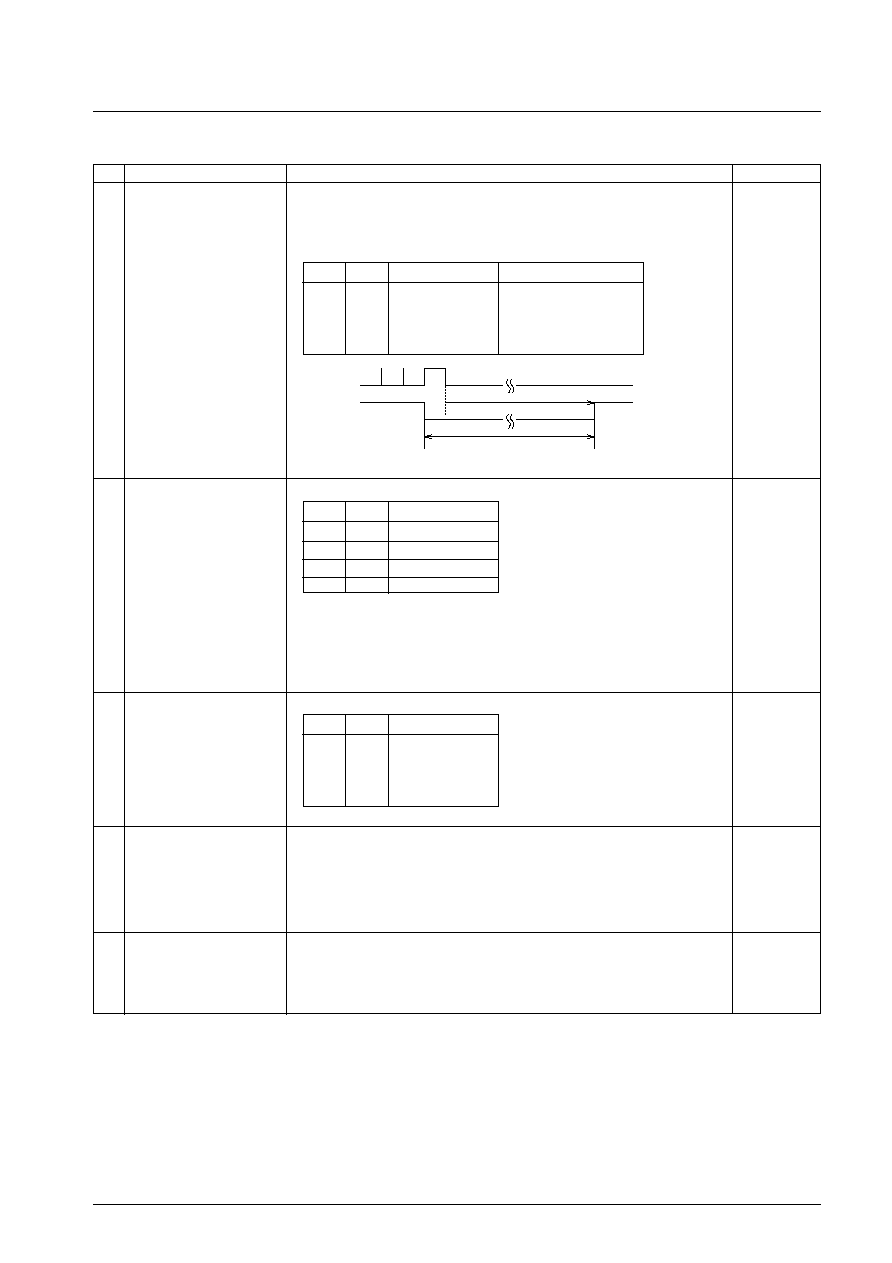
Procedures for Input and Output of Serial Data
Data I/O is handled through the Computer Control Bus (CCB), SANYO's audio IC serial bus format. This IC uses CCB
with 8-bit addressing.
I/O mode
Address
Description
B0
B1
B2
B3
A0
A1
A2
A3
[1]
IN1
0
0
0
1
0
1
0
0
∑ Control data input (serial data input) mode.
∑ 32-bit data input
[2]
IN2
1
0
0
1
0
1
0
0
∑ Control data input (serial data input) mode.
∑ 32-bit data input
[3]
OUT
0
1
0
1
0
1
0
0
∑ Data output (serial data output) mode.
∑ The bit count output is equal to the clock cycle count.
First Data IN1/2
B0
B1
B2
B3
A0
A1
A2
A3
CE
CL
DI
DO
First Data OUT
A13310
I/O mode setting
i) Serial Data Input (IN1/IN2)
ii) Serial data output (OUT)
*1: Because the DO pin is an N-channel open drain pin, the data transition time varies according to the pull-up resistance
and the board capacitance.
*2: The DO pin is normally open.
B0
B1
B2
B3
A0
A1
A2
A3
P0
P1
P2
P3
CTS0 CTS1 GT0
GT1
tEH
tEC
tES
tHD
tSU
tSUtHDtEStECtEH 0.45s
tLC 0.45s
tLC
CE
CL
DI
A13311
B0
B1
B2
B3
A0
A1
A2
A3
I7
I6
I5
I4
AD13 AD12 AD11 AD10
tEH
tEC
tES
tHD
tSU
tSUtHDtEStECtEH 0.45s
tLCtDH 0.2s (*1)
tDH
tDC
CE
CL
DI
DO
(*2)
(*2)
A13312
Internal data
LA17000M
No. 6522-18/54
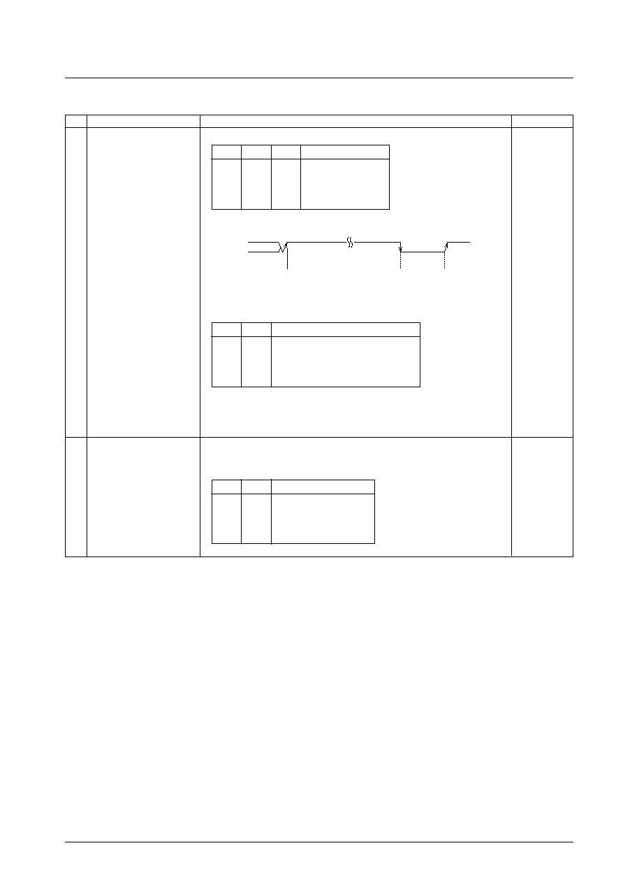
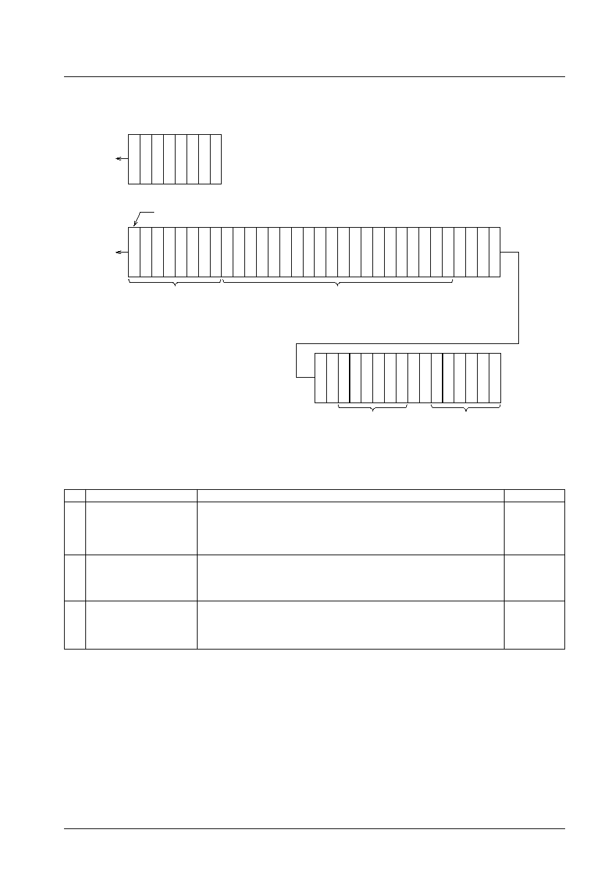
DI Control Data (Serial Data Input) Configuration
[1] IN1
0 0 0 1 0 1 0 0
P0
(1) P-CTR
(2) PD-C
(3) R-CTR
(4) DO-C
(5) ADC
(6) U-CTR
P1
P2
P3
P4
P5
P6
P7
P8
P9
P10
P11
P12
P13
P14
P15
SNS
DVS
PDC0
PDC1
R0
R1
R2
R3
DT0
DT1
ADS
CTE
CTS0
CTS1
GT0
GT1
First Data IN1
DI
A13313
1 0 0 1 0 1 0 0
SEEKSW
SDSTSW
(7) I/O-C
(8) SEEK-PORT
(9) SDST-PORT
(5) ADC
(10) O-PORT
(6) U-CTR
(4) DO-C
(11) U/I-C
(12) UNLOCK
(13) XTAL
(14) DZ-C
(16) TEST
(15) PD-L
I/O-1
I/O-2
1
1
ADI0
ADI1
OUT0
OUT1
OUT2
OUT3
0
0
CTP
CTC
HCTR
1
IL0
IL1
ULD
UL0
UL1
XS0
XS1
XB
DZ0
DZ1
TEST0
TEST1
TEST2
DLC
First Data IN2
DI
A13314
Address
[2] IN2 Mode
Address

LA17000M
No. 6522-19/54
Description of DI Control Data
No.
Control block/Data
Description
Related data
Programmable divider data
∑ This data sets divisor for the programmable divider. P15 is a binary value that is
designated as the MSB. The LSB changes depending on DVS and SNS.
P0 to P15
* DVS = 1 (DVS = 0: Prohibited)
∑ These values select the signal input pin (PLL IN) for the programmable divider,
and switch the input frequency range.
DVS, SNS
* For details, refer to "Programmable Divider Configuration."
Sub-charge pump
∑ This data controls the sub-charge pump.
control data
PDC, PDC1
* The sub-charge pump can be used to form a high-speed lockup circuit in
combination with PD0 and PD1 (main charge pump).
∑ For details, refer to the page on charge pump.
Reference divider data
∑ This is the reference frequency (fref) selection data.
R0 to R3
*1: Prohibited when X'tal OSC = 10.25 MHz.
*2: PLL INHIBIT (backup mode)
The programmable divider block stops, the PLL IN pin is pulled down to
GND, and the charge pump output goes to the floating state.
Continued on next page.
DVS
SNS
ISB
Divisor setting (N)
1
1
P0
272 to 65535
DVS
SNS
Input pin
Input pin frequency range
1
1
PLLIN
10 to 160 MHz
PDC1
PDC0
Subcharge pump status
0
*
High impedance
1
0
Charge pump on (when unlocked)
1
1
Charge pump on (normal operation)
R3
R2
R1
R0
Reference frequency
0
0
0
0
Prohibited
0
0
0
1
50
0
0
1
0
25
0
0
1
1
25
0
1
0
0
12.5
0
1
0
1
6.25
0
1
1
0
3.125
0
1
1
1
3.125
1
0
0
0
10
1
0
0
1
9 *1
1
0
1
0
5
1
0
1
1
1
1
1
0
0
9 *1
1
1
0
1
30 *1
1
1
1
0
*2 PLL INHIBIT + X'tal OSC STOP
1
1
1
1
*2 PLL INHIBIT
UL0, UL1,
DLC
(2)
(1)
(3)
LA17000M
No. 6522-20/54
Continued from preceding page.
No.
Control block/Data
Description
Related data
DO, I/O-5 pin control data
∑ This data determines the output on the DO pin and the I/O-5 pin.
ULD
DT0, DT1
IL0, IL1
end-AD: End of conversion by the A/D converter
end-UC: End of conversion by the general-purpose counter
* 1
* However, if the I/O-1 and I/O-2 pins are specified as output ports, these pins
are open.
Note: Cannot be used when X'tal OSC is set to STOP. (DO does not change.)
[When the reference divider data: R3 = R2 = R1 = 1 and R0 = 0]
A/D converter control data
∑ A/D converter conversion start data.
ADS = 1: A/D conversion reset and start
0: A/D conversion reset
ADS
ADI0
Continued on next page.
ULD
DT1
DT0
DO pin
0
0
0
Low when unlocked
0
0
1
end-AD
0
1
0
end-UC
0
1
1
IN (*1)
I/O-1
I/O-2
(4)
(5)
DO
CEHi
A13315
Start
End
(I-1 changes)
IL1
IL
IN
0
0
Open
0
1
I-1 (pin status)
1
0
I-2 (pin status)
1
1
If I-1 changes, DO goes low. (Note)
ADI1
ADI0
AD input pin
1
1
Stopped
1
0
ADC0
0
1
Not usable
0
0
Not usable

LA17000M
No. 6522-21/54
Continued from preceding page.
No.
Control block/Data
Description
Related data
∑ This data sets the general-purpose counter input pin (HCTR).
∑ General-purpose counter measurement start data
CTE = 1: Count start
= 0: Count reset
∑ This data determines the measurement time (frequency mode) and number of
periods (period mode) for the general-purpose counter.
∑ CTP = 0: When a count reset is executed (CTE = 0), the general-purpose
counter input is pulled down.
= 1: When a count reset is executed (CTE = 0), the general-purpose
counter input is not pulled down, and the wait time is reduced.
However, immediately after CTP = 1 is set, the start of the count
must wait until the general purpose counter input pin is biased.
∑ The input sensitivity is reduced when CTC = 1. (Sensitivity: 10 to 30 mVrms)
I/O port control data
∑ This data specifies whether an I/O port is an input port or an output port.
"data"= 0: Input port
= 1: Output port
I/O-1 to I/0-2
* During a power-on reset, I/O-0 and I/O-2 become input ports.
STSD SW becomes an output port.
∑ This data determines the status of the SEEK SW pin.
"data" = 0: 2.5[V] output
SEEK SW
* This pin is open and the midpoint bias is output by an external circuit.
"data" = 1: 0[V] or 5[V] output
* Determined by the OUT0 data.
∑ AM/FM SD, FM-ST IND output dual-purpose pin
SDST SW
"data" = 0: Fixed
= 1: Prohibited
Output port data
∑ This data determines the output on output ports O-0 through O-3.
"data" = 1: Open or Hi
OUT0 to OUT2
= 0: Low
* Invalid if specified as an input port or unlocked output.
∑ This data converts the general-purpose counter pin to an input port.
HCTR = 0: Prohibited
= 1: HCTR (general-purpose counter)
Continued on next page.
CTS1
Measurement time
Measurement mode
1
HCTR
Frequency
0
--
Not measured
HCTR
(6)
Frequency measurement mode
Period
GT1
GT0
Measurement Wait time (ms)
measurement
time (ms)
CTP = 0
CTP = 1
mode
0
0
4
3 to 4
1 to 2
1 period
0
1
8
3 to 4
1 to 2
1 period
1
0
32
7 to 8
1 to 2
2 periods
1
1
64
7 to 8
1 to 2
2 periods
OUT0 to OUT3
ULD
I/O-0 to I/O-3
ULD
I/O-0 to I/O-3
ULD
I/O-0 to I/O-3
ULD
CTS1
(7)
(8)
(9)
(10)
(11)
General-purpose counter
control data
CTS0, CTS1
CTE
GT0, GT1
CTP
CTC
General-purpose counter
input control data
HCTR
LA17000M
No. 6522-22/54
Continued from preceding page.
No.
Control block/Data
Description
Related data
Unlock detection data
∑ This data selects the phase error (¯E) detection width that is used for evaluating
PLL lock.
If a phase error that exceeds the ¯E detection width in the following table is
generated, the signal is deemed to be unlocked. When the signal is unlocked,
the detection pin (DO or I/O-5) goes low.
UL1, UL0
∑ This is the crystal oscillator selection data.
* When a power-on reset is executed, 10.25 MHz is selected.
∑ Crystal oscillator buffer (XBUF) output control data.
XB = 0: Buffer output: OFF (This mode is selected when a power-on reset is
executed.)
XB = 1: Buffer output ON
* For FM reception (using the PD0 pin), XBUF output must be off.
∑ This data controls the phase comparator dead zone.
∑ When a power-on reset is executed, DZA is selected.
∑ This data is used to force the charge pump output to the low level (V
SS
level).
DLC = 1: Low level
= 0: Normal operation
* If a deadlock occurs because the VCO control voltage (Vtune) is 0 V and VCO
oscillation is stopped, it is possible to escape the deadlock by forcing the
charge pump output to low level and setting Vtune to V
CC
.
When a power-on reset is executed, normal operation mode is selected.
∑ This is the IC test data.
Set TEST0 = 0.
TEST1 = 0
TEST2 = 0
* When a power-on reset is executed, all the test data is set to zero.
(12)
ULD
DT0, DT1
R0 to R3
(13)
UL1
DT0
¯E detection width
Detection pin output
0
0
Stop
Open
0
1
0
Direct output of ¯E
1
0
±0.5
µ
s
Extend ¯E by 1 to 2 ms
1
1
±1
µ
s
Extend ¯E by 1 to 2 ms
Unlocked output
E
DO
1 to 2ms
A13316
XS1
XS0
X'tal OSC
0
0
Prohibited
0
1
Prohibited
1
0
10.25 MHz
1
1
10.35 MHz
DZ1
DZ0
Dead zone mode
0
0
DZA
0
1
DZB
1
0
DZC
1
1
DZD
(14)
(15)
(16)
Extention
Crystal oscillator circuit
XS0, XS1
XB
Phase comparator control
data
DZ0, DZ1
Charge pump control data
DLC
IC test data
TEST0
TEST1
TEST2
LA17000M
No. 6522-23/54
DO Output Data (Serial Data Output) Configuration
[3] OUT mode
0 1 0 1 0 1 0 0
(2) U-CTR
(1) IN-PORT
I3
I2
I1
I0
C19
C18
C17
C16
C15
C14
C13
C12
C11
C10
AD05
AD04
AD03
AD02
AD01
AD00
C9
C8
C7
C6
C5
C4
C3
C2
C1
C0
(3) ADC0
(4) ADC1
First Data OUT
DI
DO
A13317
Address
: "0" data
No.
Control block/Data
Description
Related data
I/O port data
∑ I0 to I3 is the latched data reflecting the status of the input ports: I/O-0 to I/O-3.
The data is latched at the point that data output mode is set.
I3 to I0
The pin status is latched regardless of the input/output specification.
Pin status = Hi: 1
Low: 0
General-purpose counter
∑ C19 to C0 is the latched data reflecting the contents of the general-purpose
binary data
counter (a 20-bit binary counter).
C19
MSB of binary counter
C19 to C0
C0
LSB of binary counter
A/D converter
∑ AD05 to AD00 is the latched data reflecting the results when the ADC0 pin
input signal undergoes AD conversion.
AD05
MSB
AD05 to AD00
AD00
LSB
(1)
(2)
(3)
I/O-1 to I/O-2
SEEK SW
HCTR
CTS0
CTS1
CTE
ADI1
ADS
ADC0 data
LA17000M
No. 6522-24/54
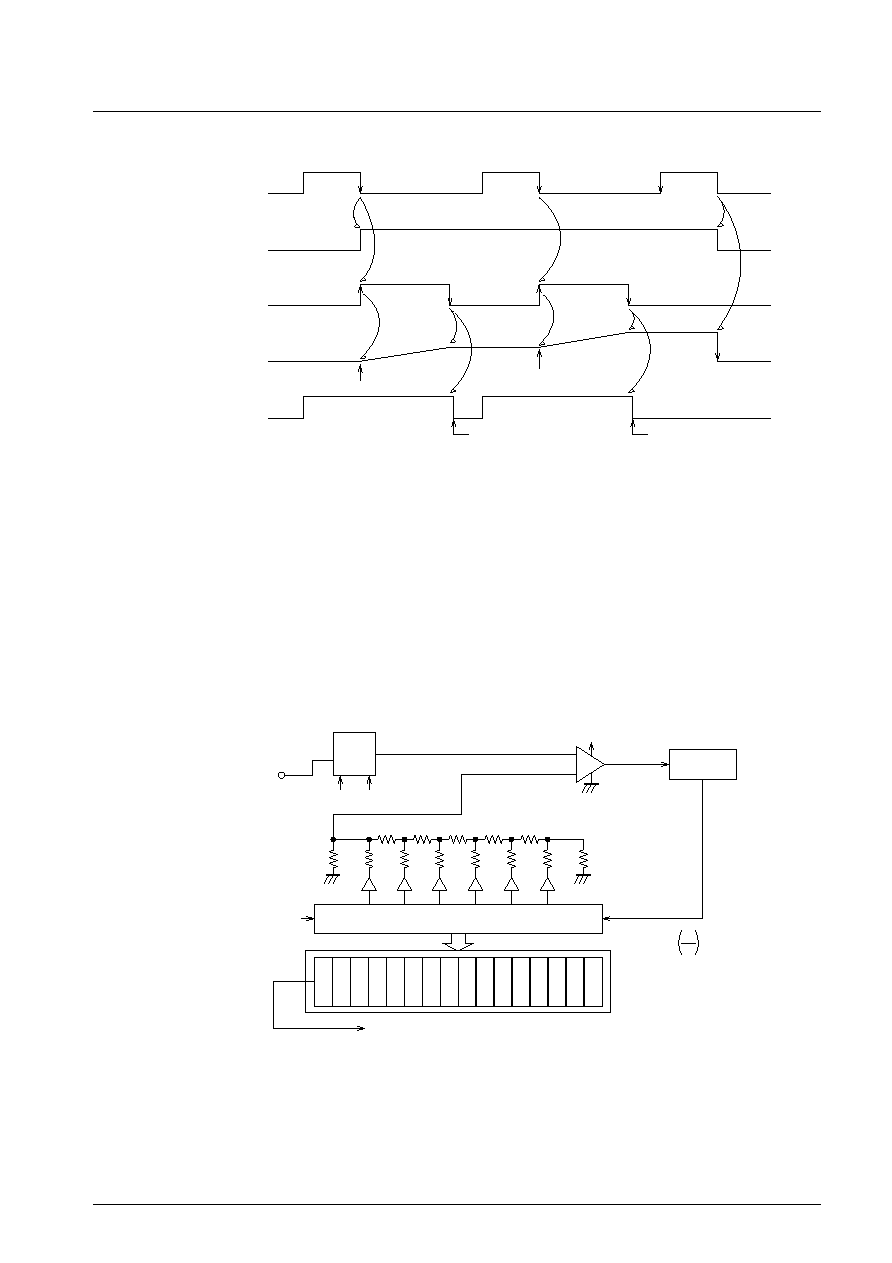
Programmable Divider Configuration
DVS SNS
Input pin
Divisor setting (N)
Input frequency range
(A)
1
*
PLL IN
272 to 65535
10 to 160 MHz
Minimum input sensitivity f[MHz]
(A) PLL IN
10
f < 130
130
f <160
40 mVrms
70 mVrms
General-purpose Counter Configuration
In the LA17000M, the general-purpose counter consists of a 20-bit binary counter. The count results can be read
through the DO pin, MSB first.
When using the general-purpose counter for cycle measurement, the measurement period can be selected from among 4,
8, 32, and 64 ms through the GT0 and GT1 data. The cycle of the signal that is input to the HCTR pin or the LCTR pin
can then be measured by counting the number of pulses that are input to the general-purpose counter within this mea-
surement period.
When using the general-purpose counter to measure a cycle, it is also possible to measure the cycle of a signal that is
input to the LCTR pin according to the number of check signals (refer to the "Check Signal Frequency" table below)
input to the general-purpose counter within one or two cycles of the signal that is input to the LCTR.
Check Signal Frequency
X tal OSC
10.25 MHz
10.35 MHz
fref = 30, 9, 3 kHz
fref other than 30, 9, 3 kHz
Check signal
10.25 kHz
1030 kHz
1150 kHz
CTS1
Input pin
Measurement mode
Frequency range
Input sensitivity
S1
1
HCTR
Frequency
0.4 to 25.0 MHz
40 mVrms *1
*1 CTC = 0: 40 mVrms; however, when CTC = 1, the frequency range is HCTR: 8 to 12 MHz
CTC = 1: 70 mVrms
PLL IN
4bits
(A)
12bits
fvco/N
fref
fvco = fref ◊ N
PD
E
Swallow
Counter
Programmable
Divider
A13318
HCTR
0
to
3 4
to
7 8
to
11 12
to
1516
to
19
4/8/32/64
ms
GT
(FIF)
L
S
B
M
S
B
CTE
C = FIF ◊ GT
GT1, GT0
A13319
1
2
CTS
General-purpose counter
(20-bit binary counter)
DO pin

LA17000M
No. 6522-25/54
CTC data: This is the input sensitivity switch data; when CTC = 1, the input sensitivity is degraded.
HCTR: Minimum input sensitivity standard f [MHz]
CTC
0.4
f < 8
8
f < 12
12
f < 25
0 (Normal mode)
40 mVrms
40 mVrms
40 mVrms
(1 to 10 mVrms)
1 (Degraded mode)
--
70 mVrms
--
(30 to 40 mVrms)
--: Not stipulated (operation not guaranteed)
( ): Actual performance estimates (reference value)
CTP data: This is data that determines the status of the general-purpose counter input pin (HCTR/LCTR) when a
general-purpose counter reset (CTE = 0) is executed.
CTP = 0: Pulls down the general-purpose counter input pin.
= 1: Does not pull down the general-purpose counter input pin, reducing the wait time to 1 or 2 ms.
When setting CTP = 1, do so at least 4 ms prior to starting the count (CTE = 1). If the counter is not to be
used, set CTP = 0.
IF Counter Operation
Before starting counting with the general-purpose counter, the general-purpose counter must first be reset by setting CTE
= 0. The general-purpose counter is made to start counting by setting serial data CTE = 1. The serial data is finalized
within the PLL by changing CE from high to low, but input to the HCTR pin must be started within the wait period after
CE is sent low at the very latest. After measurement ends, the count results from the general-purpose counter must be
read while CTE = 1. (Once CTE is set to zero, the general-purpose counter is reset.) Furthermore, the signal that was
input to the HCTR pin is passed through to the general-purpose counter after having been divided by 1/2 internally.
Therefore, the general-purpose count results are actually 1/2 the actual frequency of the signal that was input to the
HCTR pin.
Frequency measurement mode
Cycle
GT1
GT0
Measurement Wait time
measurement
time
CTP = 0
CTP = 1
mode
0
0
4 ms
3 to 4 ms
1 cycle
0
1
8
1 to 2 ms
1
0
32
7 to 8 ms
2 cycles
1
1
64
CE
A13320
40 mVrms or more*
(when measuring frequency)
* CTC = 0: 40 mVrms
CTC = 1: 70 mVrms
Signal input
Measurement
time
Wait time
Frequency measurement time
CTE = 1
data
LA17000M
No. 6522-26/54
Integrated Count
* CTE: 0
∑ General-purpose counter reset
1
∑ General-purpose counter start
∑ Setting to "1" again causes a restart.
When using integrated counting, the count value is accumulated in the general-purpose counter.
Be careful about counter overflows.
Count value: 0
H
to FFFFF
H
(1048575)
When using integrated counting, resending serial data (IN1) with CTE = 1 restarts measurement with the
general-purpose counter, and the count results are added to the previous count results.
A/D Converter Configuration
This is a 6-bit successive-approximation converter with a conversion time of 0.56 ms. Full scale (when the data is 3F
H
)
is (63/96) x V
DD
.
Count end
CE
CTE=1
Start
Restart
Reset
CTE=1
CTE=0
A13321
Internal data latch
(CTE)
General-purpose counter
(integration)
ADO0
ADO1
ADO2
ADO3
ADO4
ADO5
ADS
ADC0
2R
MSB
LSB
2R
2R
R
R
R
R
R
-
2R
2R
2R
2R
2R
ADI0 ADI1
Vref
63
96
Vref max=◊VDD
VDD
A13322
Multi-
plexer
Comparator
Evaluation
circuit
Decoder
REGISTER
: "0" data
DO pin
GT
end-UC
LA17000M
No. 6522-27/54
ADI1
ADI0
Input pin
1
1
Prohibited
1
0
ADC0
0
1
Prohibited
0
0
Prohibited
Charge Pump Configuration
PDC1 PDC0
PDS (sub-charge pump status)
0
*
High impedance
1
0
Charge pump on (when unlocked)
1
1
Charge pump on (at all times)
If the unlocked state is detected during a channel change, the PDS (sub-charge pump) operates, R1
R1M/R1S, the
low-pass filter time constant is reduced, and lockup is accelerated.
* Unlock detection data: UL1 = 1 must be set. This sets the unlock detection width to "±0.5
µ
s" or "±1
µ
s" mode; if a
phase difference that is greater than the value in question is detected, the signal is unlocked and the sub-charge pump
operates. As the locked condition is approached and the phase difference falls to less than the unlocked detection
width, the sub-charge pump stops operating (goes to high impedance).
* Since the PLL block in the LA17000M does not provide an
external pin for ADI1, the function cannot be used. ADI0
is linked directly to the pin 34 MRC sensor output, and is
used exclusively for multipath signal intensity detection.
Conversion start
A13324
A13323
PDC0 PDC1
Unlock
PDS
PD1
DLC
CTS=1
tWA1
tAD
ADC0
tWA10.08 to 0.11ms
tWA20.08 to 0.09ms
tAD 0.56 to 0.62ms
end-AD
fvco/N
CE
fref
Clock
UL0
UL1
DZ1
DZ0
Phase
Detector
Unlock
Detector
and
Subcharge
Pump Cont
(SUB)
(MAIN)
Conversion
Conversion end
D0, I/O-5 pin
DLC
PD1, PDS
0
Normal operation
1
Forced low
A13325
PD0
R1M
Vtune
VCC
R1S
PDS
LA17000M
No. 6522-28/54
Other Items
[1] Notes on the Phase Comparator Dead Zone
DZ1
DZ0
Dead zone mode
Charge pump
Dead zone
0
0
DZA
ON/OFF
≠ ≠0 s
0
1
DZB
ON/ON
≠0 s
1
0
DZC
OFF/OFF
+0 s
1
1
DZD
OFF/OFF
++0 s
Since correction pulses are output from the charge pump even if the PLL is locked when the charge pump is in the
ON/ON state, the loop can easily become unstable. This point requires special care when designing application
circuits.
The following problems may occur in the ON/ON state.
∑ Side band generation due to reference frequency leakage
∑ Side band generation due to both the correction pulse envelope and low frequency leakage
Schemes in which a dead zone is present (OFF/ON) have good loop stability, but have the problem that acquiring a
high C/N ratio can be difficult. On the other hand, although it is easy to acquire a high C/N ratio with schemes in
which there is no dead zone, it is difficult to achieve high loop stability. Therefore, it can be effective to select DZA
or DZB, which have no dead zone, in applications which require an FM S/N ratio in excess of 90 to 100 dB, or in
which an increased AM stereo pilot margin is desired. On the other hand, we recommend selecting DZC or DZD,
which provide a dead zone, for applications which do not require such a high FM signal-to-noise ratio and in which
either AM stereo is not used or an adequate AM stereo pilot margin can be achieved.
Dead Zone
The phase comparator compares fp to a reference frequency (fr) as shown in Fig. 1. Although the characteristics of
this circuit (see Fig. 2) are such that the output voltage is proportional to the phase difference ¯ (line A), a region
(the dead zone) in which it is not possible to compare small phase differences occurs in actual ICs due to internal
circuit delays and other factors (line B). A dead zone as small as possible is desirable for products that must provide
a high S/N ratio.
However, since a larger dead zone makes this circuit easier to use, a larger dead zone is appropriate for popularly-
priced products. This is because it is possible for RF signals to leak from the mixer to the VCO and modulate the
VCO in popularly-priced products in the presence of strong RF inputs. When the dead zone is narrow, the circuit
outputs correction pulses and this output can further modulate the VCO and generate beat frequencies with the RF
signal.
[2] Notes on the PLL IN and HCTR pins
Coupling capacitors must be placed extremely close to these pins. The capacitance should be about 100 pF. If a
capacitor with a capacitance of 100 pF or less is not used with HCTR in particular, there will be a long wait until the
bias level is reached, which may sometimes cause miscounting.
[3] Notes on IF counting
When using the general-purpose counter for IF counting, be certain to have the microcontroller determine whether
the IF-IC SD (Station Detector) signal is present or not, and to turn on the IF count buffer output and conduct the
count, but only if the SD signal is present. Conducting an auto search using only the IF count is not reliable, since
there is a possibility of stopping even where there is no station due to leaked output from the IF count buffer.
[4] Using the DO pin
Aside from data output mode, the DO pin can also be used to check for the completion of counting by the general-
purpose counter, unlock detection output, and to check for changes in the input pins. It is also possible to input the
status of the input pins (I/O-1, I/O-2) to the controller, unchanged, via the DO pin.
A13326
A13327
Dead Zone
RF
fr
fp
Reference Divider
Programmable Divider
Phase
Detector
MIX
(ns)
(B)
(A)
V
LFP
VCO
Leak
Fig. 1
Fig. 2
LA17000M
No. 6522-29/54
[5] Cautions concerning the use of XBUF
When the XBUF output is on (AM up conversion is being used), the XBUF signal may leak to the adjacent pins
(PD0, I/O-3), so do not use PD0 and I/O-3 for AM reception control. (Use the PD1 pin for the AM reception charge
pump.) When using PD0 and I/O-3 for FM reception control, the XBUF output must be turned off (XB data = 0).
[6] Power supply pins
To filter out noise, insert a capacitor of at least 2000 pF between the power supply pins V
DD
and V
SS
. The capacitor
must be located as close to the pins as possible.
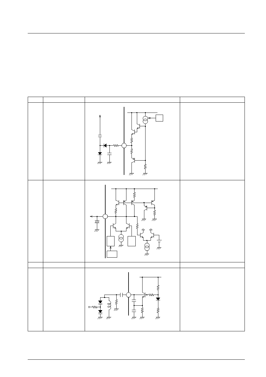
Tuner Block Pin Description
Pin No.
Function
Equivalent circuit
Description
1
Antenna damping drive
pin.
2
RF AGC
FET 2nd gate voltage control pin.
3
F.E.GND
4
OSC
OSC pin with built-in Tr. capacitor for
oscillator circuit.
1
2
ANT
1000pF
1000pF
100
100
300
VCC
RF
AGC
N
AGC
DET
W
AGC
DET
KEYED
AGC
ANT
DAMPING
DRIVER
VCC
VCC
12k
FET
2ND GATE
4
VCC
18pF
20pF
60pF
VT
The antenna damping current flows
to this pin when the pin 2: RF AGC
voltage is V
CC
-V
D
.
A13328
A13329
A13330
Continued on next page.
Pin 62

LA17000M
No. 6522-30/54
Continued from preceding page.
Pin No.
Function
Equivalent circuit
Description
6
F.E.V
CC
, AM/FM switch
Pin 6 is shared for FM F.E.V
CC
and
pin
the AM/FM SW circuit.
7
AM OSC
First OSC for AM.
Permits oscillation up to the SW
band.
ALC circuit connected.
8
Noise AGC sensitivity
9
AGC adjusting pin
10
AM 2nd OSC
A13366
3
6
-
FM.F.E
AGC
SD
VCC
510
100k
3.3V
GND
8V
AM/FM Switch
Circuit
V6 voltage
Mode
8V
FM
OPEN
AM
8
9
7
VCC
A L C
3k
15k
3k
3k
1M
0.01F
0.47F
200
Pin 8 is the noise sensitivity setting
pin. After setting a moderate field
(approximately 50 dB
µ
), use the pin 9
AGC adjusting pin to make the
setting for weak fields (approximately
20 to 30 dB
µ
).
Shared pin.
CF selectivity switch.
Select either 10.7 MHz 1st IF input
pin 72 or pin 78.
∑ A second local oscillation signal is
injected by the PLL XBuffer.
* The PLL X'tal is as follows:
AM 9 kHz step 10.35 MHz
AM 10 kHz step 10.25 MHz
(NDK AT-51 type: XTAL oscillator)
10
10k
10k
10k
51k
SW
10k
5.6V
100pF
5V
TO 2nd
MIX
PLL
XBuffer
A13331
A13332
A13367
Continued on next page.
SWON
pin 78 input
SOWOPen pin 78 input
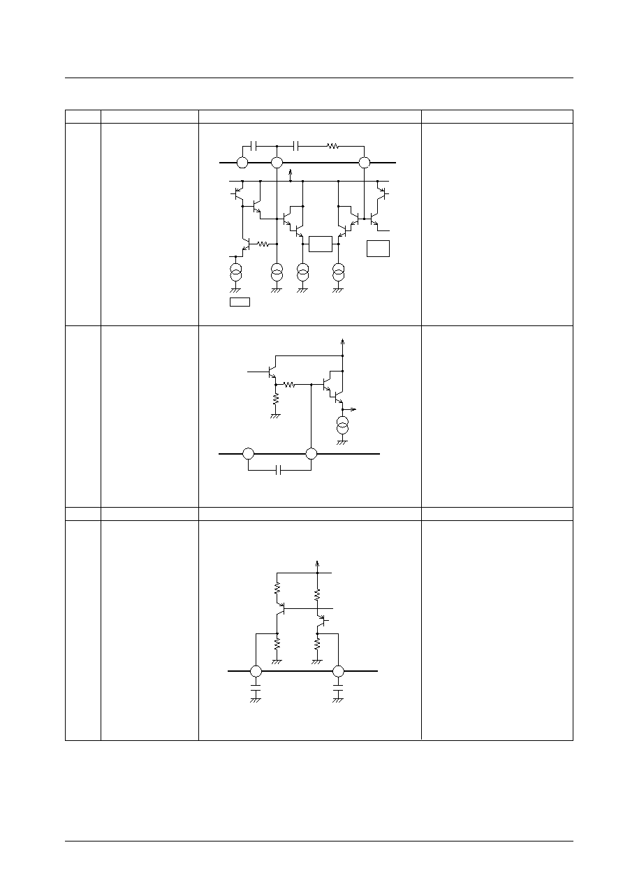
LA17000M
No. 6522-31/54
Continued from preceding page.
Pin No.
Function
Equivalent circuit
Description
11
Memory circuit pin
12
Memory circuit pin
13
Pilot input
Pin 13 - PLL circuit signal input pin.
14
N.C, MPX, MRC, GND
GND for N.C/MPX/MRC circuit.
15
MPX output (LEFT)
De-emphasis
16
MPX output (RIGHT)
50
µ
s; 0.015
µ
F
75
µ
s; 0.022
µ
F
A13333
A13334
A13335
Continued on next page.
Memory circuit used when the noise
canceller is in operation.
13
12
11
VCC
3.9k
0.01F
6800pF
LPF
15
12
13
30k
3.3k
3.3k
VCC
VCC
PLL
N.C
0.01F
0.015F
0.015F
16
Gate
circuit
Differential
amp
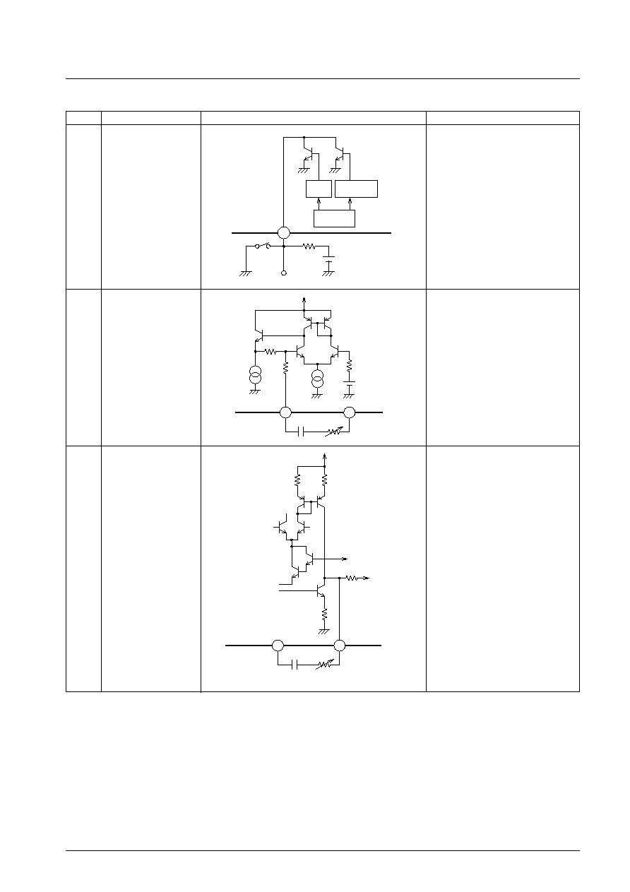
LA17000M
No. 6522-32/54
Continued from preceding page.
Pin No.
Function
Equivalent circuit
Description
17
SD pin
Stereo indicator
35
36
Pin 36 pilot canceller signal output
pin.
A13342
A13336
A13337
Continued on next page.
For FM:
V17 switches among three modes
according to the following voltages.
5 V: Operates in conjunction with
the SD pin and the IF count
buffer.
2.5 V:Operates as SD pin in forced
SD mode. RDS AF9AR.
0 V: Reception mode stereo
indicator
For AM: (two modes: 0 and 5 V)
5 V: Operates as SEEK SD pin.
0 V: Reception mode, not used
17
100k
VDD
Stereo
indicator
SEEK/STOP
switch
AM/FM
SD
The pilot signal level requires
adjustment since it changes
according to variations in the IF
output level, etc.
35
36
35
36
VCC
VCC
20k
10k
0.01F
0.01F
100k
1.5k
100k
6.7k
Pilot canceller signal
output
Pilot canceller signal
input
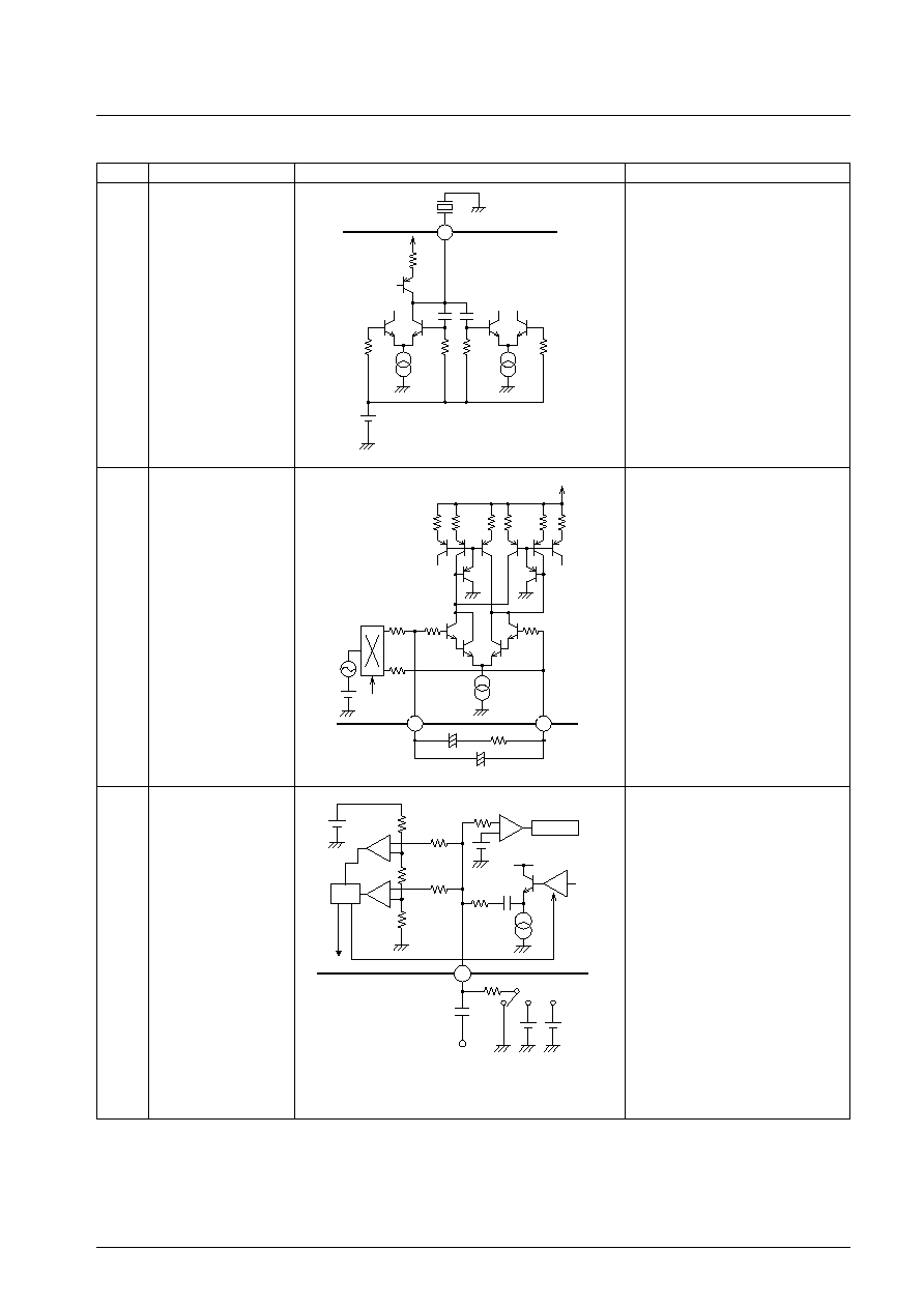
LA17000M
No. 6522-33/54
Continued from preceding page.
Pin No.
Function
Equivalent circuit
Description
37
VCO
Oscillation frequency: 912 kHz.
Murata CSB912JF108
40
PHASE COMP.
41
PHASE COMP.
38
IF count buffer
SEEK/STOP switch
A13338
A13339
A13340
Continued on next page.
40
41
37
CSB
912
JF108
VREF
10pF
15k
15k
19k
VREF
Forced
SD 2.5V
Shared pin for the IF count buffer (AC
output) and SEEK/STOP switch (DC
input).
V38 switches among three modes
according to the following voltages.
For FM:
5 V: SEEK mode
2.5 V: Forced SD mode, RDS mode
0 V: Reception mode
For AM (two modes: 0 and 5V)
5 V: SEEK mode
0 V: Reception mode
*When interference from an adjacent
FM frequency is detected:
2.5 V: Use RDS mode.
38
-
-
-
4.9V
50k
150
50F
1.3V
10k
51k
STOP
IF
BUFF.
SW
VCC
AM MUTE
SD circuit
IF count buffer
SEEK
5V
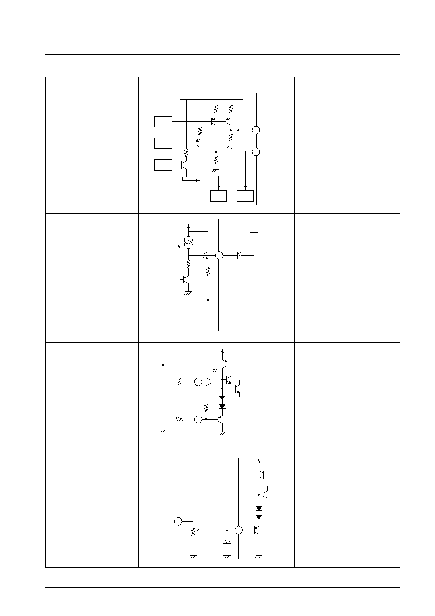
LA17000M
No. 6522-34/54
Continued from preceding page.
Pin No.
Function
Equivalent circuit
Description
42
AM/FM S-meter
Constant current drive-type S-meter
output.
48
Dedicated FM S-meter
When AM is set, pin 48 outputs a
1 mA current, which turns HCC OFF.
43
MRC control voltage
time constant
44
SNC control input pin
45
HCC control input pin
A13341
A13343
A13345
Continued on next page.
Controls sub-output with an input of 0
to 1 V.
SNC voltage is determined by the RA
and RB component voltage. This
sets the separation blend curve.
RB = 5 k
on chip
RA is external
48
42
10k
10k
VCC
AM/FM
SW
MRC
FM
S-meter
AM
S-meter
AM/FM
SW
The MRC detection time constant is
determined 1 k
and C2 when
discharging and by a constant
current of 7
µ
A and C2 when
charging.
48
44
43
43
7A
500
5k
RB
RA
1F
C2
VCC
VREF
VCC
VCC
45
VREF
VCC
A13344
Controls high frequency output with
an input of 0 to 1 V.
Control through the MRC output is
also possible.
Use at least a 100 k
resistor when
using pin 48 FM S-meter for control.
to pin 44
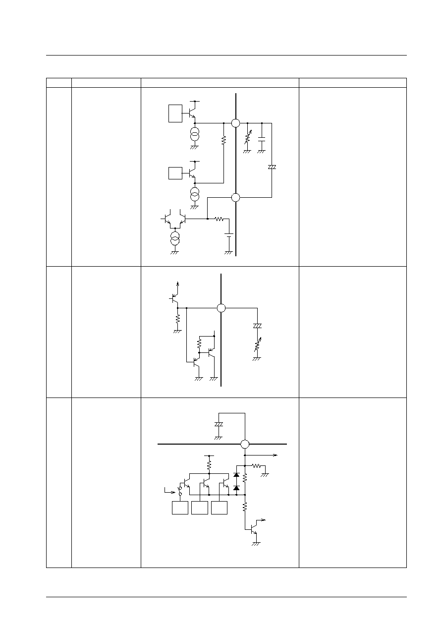
LA17000M
No. 6522-35/54
Continued from preceding page.
Pin No.
Function
Equivalent circuit
Description
46
Noise canceller input
47
AM/FM detection
output
48
IF S-meter output and
MRC DC input pin
49
Mute driver output
A13346
A13347
Continued on next page.
FM
detec-
tion
output
AM
detec-
tion
FM S-meter output block
MRC AC input block
Adjust an external 1-k
resistor to
attenuate and control the MRC AC
input.
A13348
1) The mute time constant is
determined by an external CR as
follows:
Attack time
T
A
= 10 k
◊
C1
Release time
T
R
= 50 k
◊
C1
2) Noise convergence adjustment
Fine adjustments can be made
when there is no input to the ANT
input by inserting a resistor
between pin 49 and GND.
3) Mute off function
Short pin 49 with GND using a
4-k
resistor.
47
46
48
VCC
VCC
VCC
10k
10k
1k
1F
1F
50k
4.2V
Pin 46: N.C. input
Input impedance 50 k
Pin 47: AM.FM detection output
For FM: Low impedance
For AM: 10 k
output
To improve low-band separation, use
a coupling capacitor of at least 10
µ
.
49
HOLE
DET
SOFT
MUTE
SEEK
OFF
VCC
0.1F
C1
50k
10k
50k
MUTE
AMP.
SD circuit
BAND
MUTE
MRC input
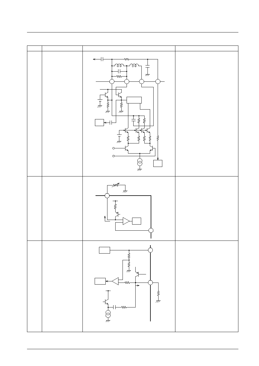
LA17000M
No. 6522-36/54
Continued from preceding page.
Pin No.
Function
Equivalent circuit
Description
50
AFC
51
QD output
52
QD input
53
V
REF
54
FM SD Adi
55
Keyed AGC
AM stereo buffer
A13349
A13350
Continued on next page.
A13351
∑ R1: Resistor that determines the
band muting function.
Increasing the value of R1 narrows
the band
Reducing the value of R1 widens
the band.
∑ Null voltage
Voltage between pins 50 and 53
during tuning:
V
50-53
= 0 V
Band muting turns on when
|V
50-53
|
0.7 V.
V
53
= 4.9V
53
52
51
50
HOLE
DET
0.1F VREF
R1
R2
VCC
VCC
C
390
1k
3pF
Quadrature
detection
Current of 130
µ
A flows from pin 54
and comparison voltage is
determined by external resistance.
The keyed AGC operates when the
voltage divided by the 6.4-k
and
3.6-k
resistors on S-meter output
pin 42 falls below the voltage
determined by the resistor between
pin 55 and GND.
Shared pin for the AM stereo decoder
IF buffer.
42
55
42
54
-
-
KEYED
AGC
SD
R
SD ADJ
130A
6.4k
3.6k
1.3V
50pF
150
90A
VCC
AM IF out
S-meter
S-meter
BAND
MUTE
1F limiter AMP
Comparator
Comparator
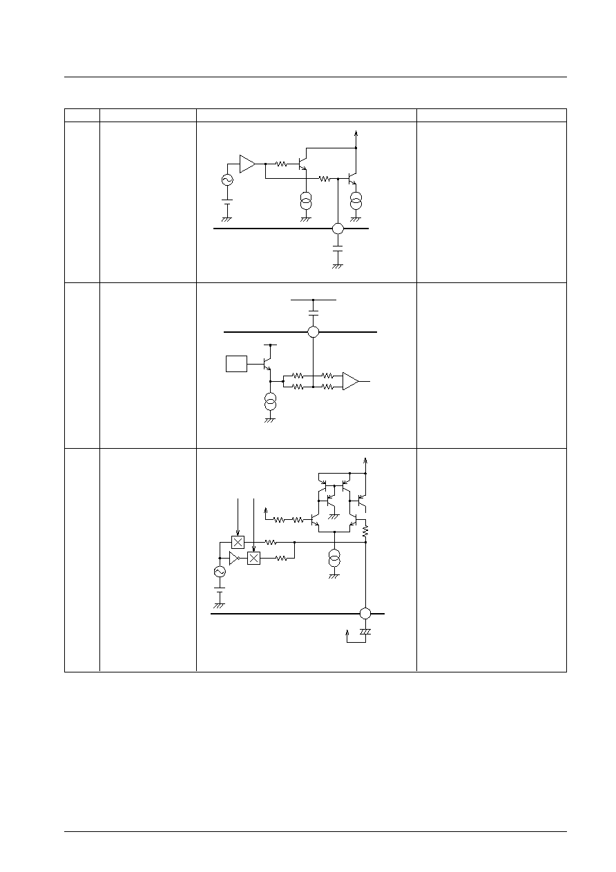
LA17000M
No. 6522-37/54
Continued from preceding page.
Pin No.
Function
Equivalent circuit
Description
57
HCC capacitor
58
AM L.C. pin
59
Pilot detector
A13352
A13353
Continued on next page.
A13354
HCC frequency characteristics are
determined by the capacitance of the
external capacitor.
In AM mode, this changes the
frequency characteristics of the
unneeded audio band below 100 Hz
in order to produce clear audio.
Note:
The capacitor for the LC must be
connected to V
CC
(pin 56) (because
the detection circuit operates with
V
CC
as a reference).
The cutoff frequency f
C
is determined
by the following formula:
f
C
= 1/2
◊
50 k
◊
C
Inserting a 1-M
resistor between
pin 59 and V
CC
forces MONO.
57
2200pF
20k
20k
VCC
59
58
-
DET
VCC
VCC
VCC
C
50k
50k
30k
30k
30k
19kHz 0∞
BIAS
1F
1k
1k
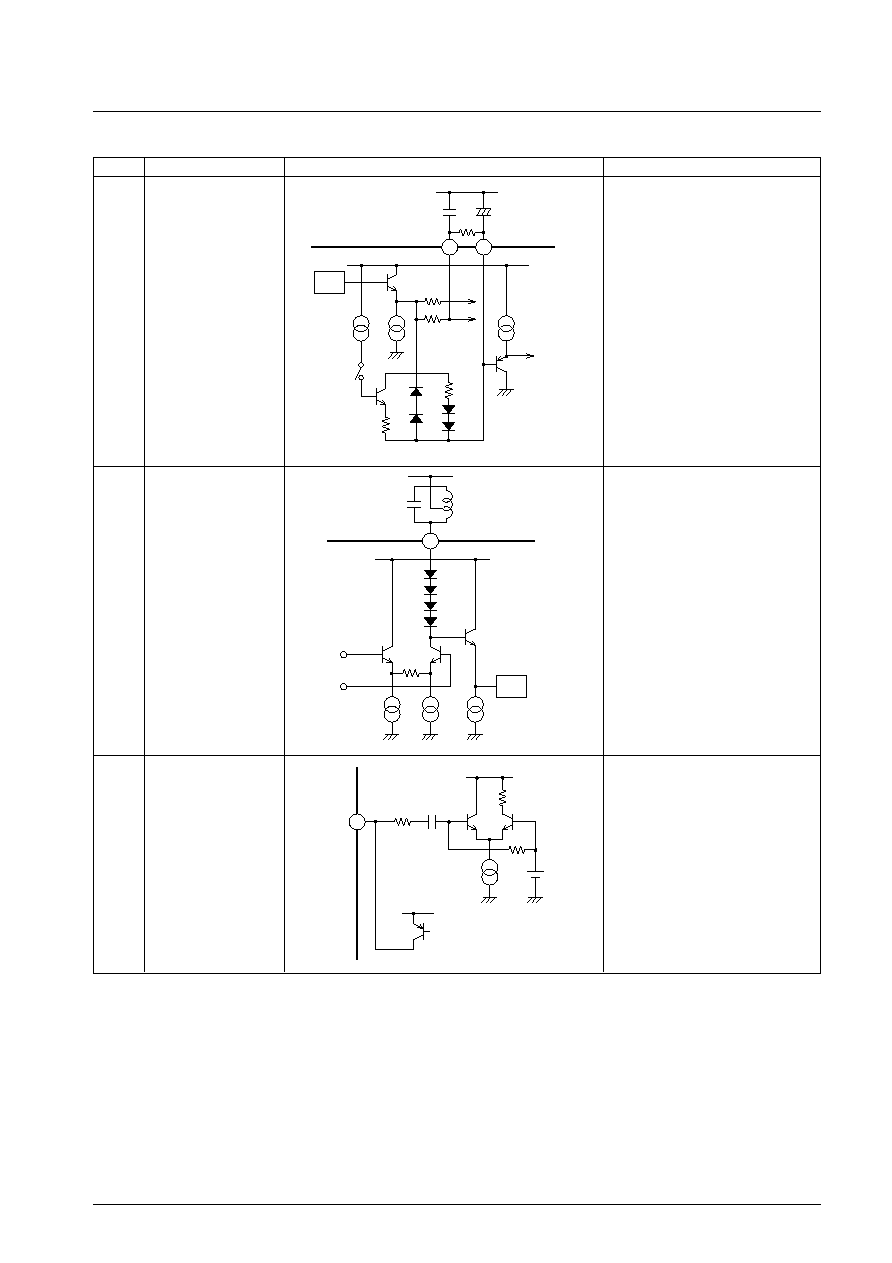
LA17000M
No. 6522-38/54
Continued from preceding page.
Pin No.
Function
Equivalent circuit
Description
60
IF AGC
61
IF output
IF amplifier load
62
AM
ANT damping
drive output
Wideband AGC input
A13355
A13356
Continued on next page.
A13357
Q1: Seek time constant switch
= 2.2
µ
F
◊
300 k
2 SEEK
= 2.2
µ
F
◊
10
Connect external C to V
CC
(because
the IF amplifier operates with V
CC
as
a reference).
I62 = 6 mA max
ANT damping current
58
DET
60
VCC
VCC
C
2.2F
0.022F
50k
50k
240k
G1
10
SEEK
ON
IF
AGC
62
61
DET
VCC
VCC
50pF
100
20k
ANT DAMPING
DRIVER
W.AGC AMP.
Pin56 V
CC
Pin56 V
CC

LA17000M
No. 6522-39/54
Continued from preceding page.
Pin No.
Function
Equivalent circuit
Description
63
FM mute on Adjust
64
RF AGC bypass
73
RF AGC
66
IF bypass
67
FM IF input
68
IF input
Input impedance 2 k
A13358
A13359
Continued on next page.
A13360
Vary the external resistor to adjust
the mute on level.
Be careful in regards to the GND
point for the limiter amplifier input C.
Ground C1 at a point that does not
increase AMR.
Inverter circuit
63
-
VCC
30k
R
140A
24
MUTE
68
66
67
64
73
-
VCC
5.6V
2.6V
10k
10k
10k
C1
0.022F
330
IF in
3.3F
47F
2k
100
RF AGC rectification capacitor
The distortion in low-frequency
modulation is determined as follows.
C64, C73
Increase
Distortion
Good
Response
Slow
C64, C73
Decrease
Distortion
Worsens
Response
Fast
A13361
For AGC
Antenna
damping
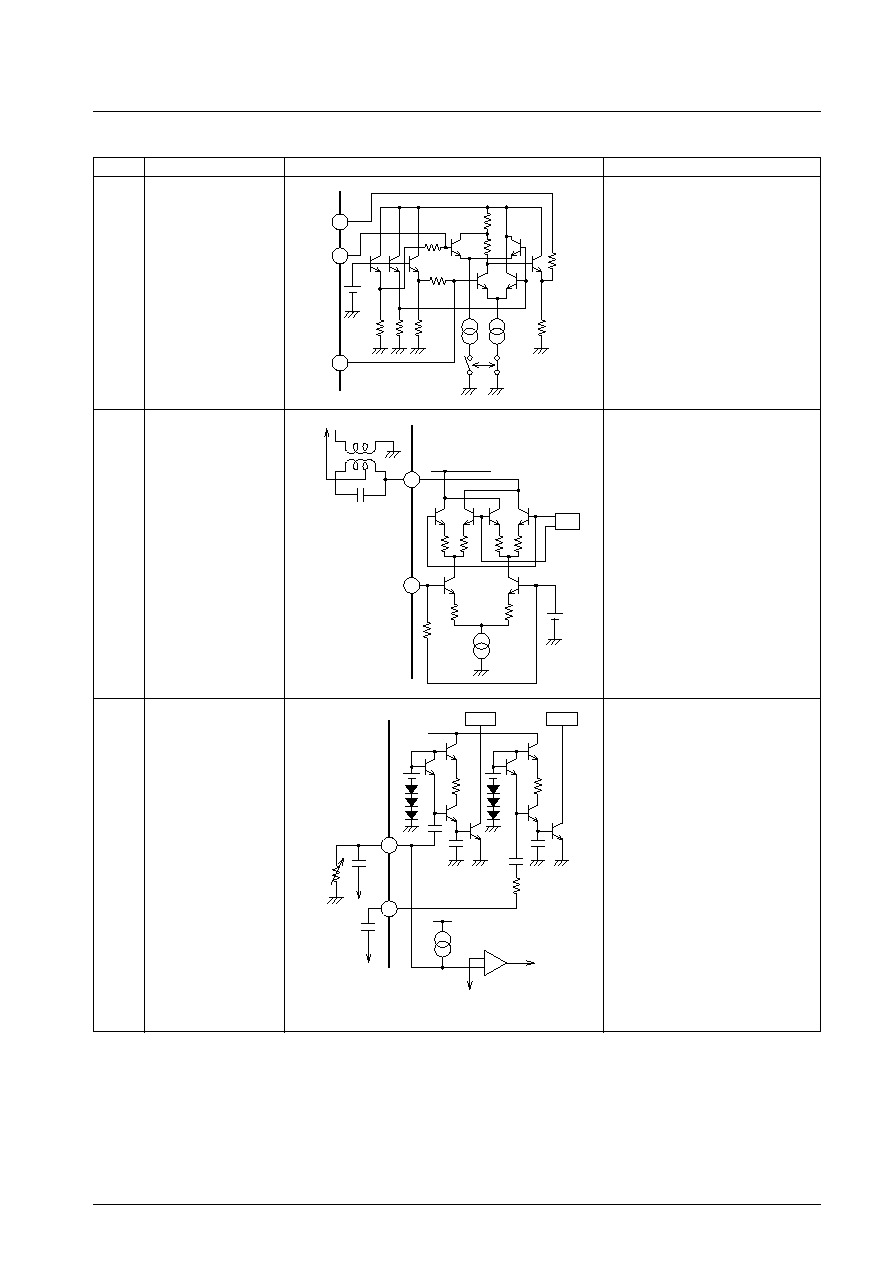
LA17000M
No. 6522-40/54
Continued from preceding page.
Pin No.
Function
Equivalent circuit
Description
69
72
78
70
MIX output 130
µ
A
65
MIX input
71
W-AGC IN
AM SD Adjust
74
N-AGC IN
mute attenuation
adjusting pin
A13362
A13363
Continued on next page.
A13364
∑ 1ST.IF amplifier I/O pin
∑ Inversion amplifier
V78 = 2 V Narrow 1st IF input
V72 = 2 V Wide 1st IF input
Input impedance
R
IN
= 330
V59 = 5.3 V
Output impedance
R
OUT
= 330
When SW1 open, SW2 short
When SW1 short, SW2 open
Switched by the CF band, switched
by voltage on pin 10.
Pin 71, 74 DC cut capacitors are on
chip.
The AGC on level is determined by
the capacitance of C1 and C2.
Pin 71 is the SD sensitivity adjusting
pin for AM.
Output current I71 = 50
µ
A, and V71
varies according to the external
resistance.
SD is put into operation by
comparing V71 with the S-meter
voltage.
Wire the MIX coil that is connected to
the pin 70 MIX output to pin 56
(V
CC
).
Pin 65 MIX input.
Input impedance
330
69
78
IF OUT
72
W IF IN
N IF IN
2.75V
300
300
500
1.3k
SW2
SW1
VCC
300
71
74
70
65
-
W-AGC
OSC
330
N-AGC
30pF
50pF
50A
AM SD
C1
MIX
IN
MIX
OUT
Pin 56
V
CC
V
CC
pin 56
Pin 77
V
CC
S-meter
IF amplifier output
IF amplifier input wide
input
IF amplifier input
narrow input
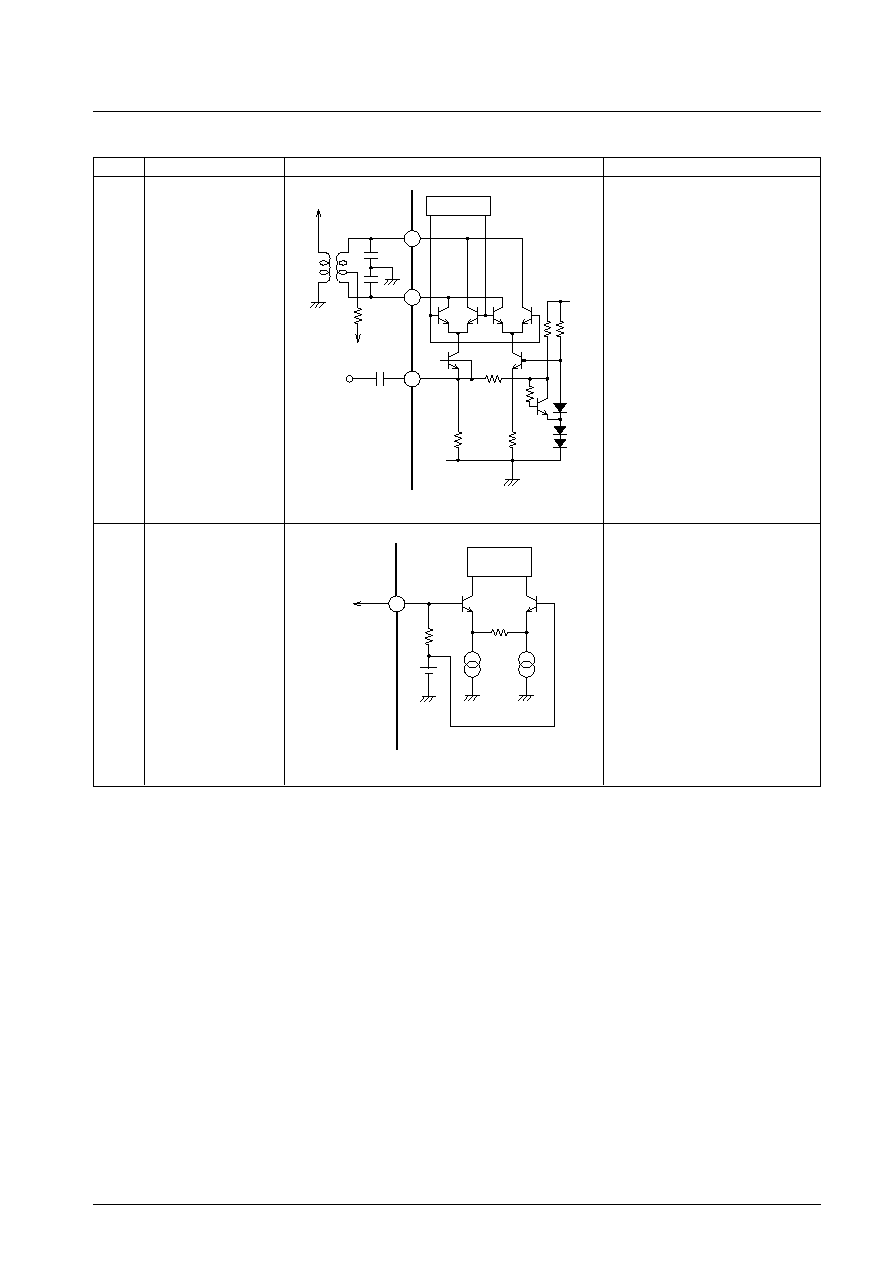
LA17000M
No. 6522-41/54
Continued from preceding page.
Pin No.
Function
Equivalent circuit
Description
75
MIX ouput
76
80
MIX input
79
1st MIX
INPUT
A13365
A13368
Double-balance type mixer
Pins 75 and 76, MIX output,
10.7 MHz output
Pin 80, MIX input
Emitter injection method and injection
amount are determined by the values
of C1 and C2.
Note:
The line for pin 80 must not approach
pins 75 and 76.
1st MIX input
Input impedance:
approximately 10 k
75
76
80
O S C
1ST.IF
30
VCC
C1
5pF
RF AMP
500
500
VCC
10k
79
AM 1st
MIX
to RF
Amp.
10k
2.1V
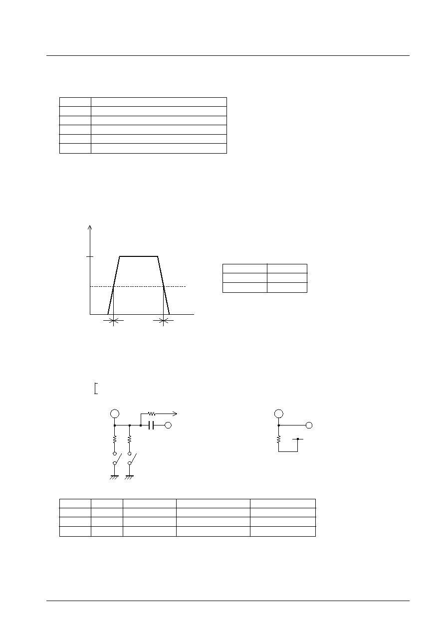
LA17000M
No. 6522-42/54
Methods for Using the LA17000M
(1) About V
CC
and GND
Pin 56
V
CC
for FM IF, AM, NC, MPX, and MRC
Pin 39
GND for FM IF and AM
Pin 14
GND for NC, MPX and MRC
Pin 77
V
CC
for FM FE, AM 1st MIX, and 1st OSC
*Pin 6
V
CC
for FM FE and AGC, and AM/FM switch
Pin 3
GND for FM FE, AM 1st MIX, and 1st OSC
(2) Notes on AM coil connection
V
CC
for the 1st OSC coil that is connected to pin 7 should have the same electric potential as pin 77.
Connect pin 61 IFT to pin 70 MIX coil. V
CC
should have the same electric potential as pin 56.
(3) AM/FM switch
Pin 6 serves as FM, FE, and RFAGC V
CC
.
(4) Relationship between pin 38 and pin 17
4-1. For FM
Pin 17
STEREO indicator and SD dual-purpose pin
Pin 38
DC input SEEK, STOP pin (control pin)
AC output IF count buffer pin
SW1
SW2
Pin 38 voltage
Pin 17
Pin 17
OPEN
OPEN
5 V
IF count buffer on
SD
ON
OPEN
2.5 V
IF count buffer on
High-speed SD
--
ON
0.7 V or less
OFF
Stereo indicator
Relationship Between Pin 38 Control Method and Output from Pins 38 and 17
V
6pin
8
3.3
AM
FM
AM
A13369
Pin 6 voltage
Mode
8
FM
OPEN
AM
IF count buffer
38
17
51k
100k
5V
51k
SW1
SW2
5V
A13370
A13371
0 to several k

LA17000M
No. 6522-43/54
Relationship between FMSD, IF count buffer output, S-meter, and mute drive output
ON as
SD
5V
OFF
OFF
SD ON
SD
ON
V38DC
V38AC
V17
V49
V54
V42
5V
2.5V
0V
A13372
Note: IF count output is off in the LA1780/81. Turn the
IF count output on in the LA17000M only.
(This is done for use in detecting interference from
adjacent frequencies.)
S-meter
R
38
larger
R
38
smaller
V49
0.7 V or
more
IF count output ON
IF count
buffer
on
Monaural
Stereo
V49
0.7 V or
more
Switch this mode for use in SD
detection in RDSAF search, etc.
Use 2.5 V mode for detecting interference
from adjacent frequencies, and confirm
the IF count frequency.
Band
mute
About FM SD
FM IF
HOLE
CLET
STEREO
IND
54
42
49
38
17
-
-
-
4.9V
R
R
R
2.5V 5V
SD
STEREO/MONO
5V
A13373
51k
Connected
directly to PLL
and I/O-3
IF count output
IF count buffer
Mute drive
output
S-
meter

LA17000M
No. 6522-44/54
4-2. For AM
Pin 71 AM, SD, Adj Pin
(5) AM STEREO support pin
5V
OFF
IF Buffer ON
SD ON
V38AC
V38DC
V17
V71
V42pin
0V
A13374
61
55
VCC
VCC
IFT
50pF 150
IF AMP.
KEYED AGC
GND
A13375
S-meter
R
71
larger
R
71
smaller
400 mVrms
450 kHz output
∑ To attenuate the pin 55 AC level, add capacitance between GND and pin 55. For example, if pin 67 is added between
GND and pin 55, the AM IF output decreases by about 6 dB.
To AM ST decoder
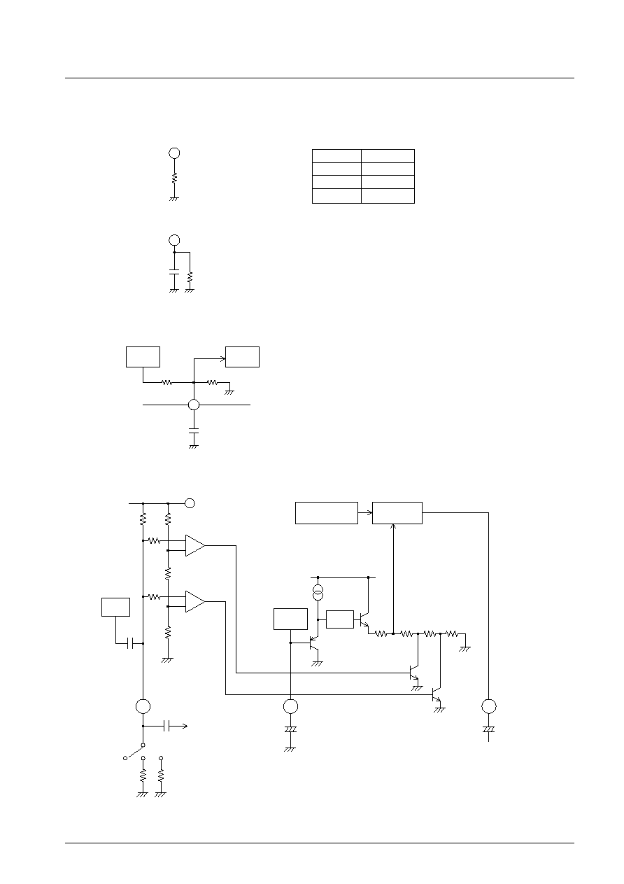
LA17000M
No. 6522-45/54
(6) About MUTE ATT
It is possible to switch to one of three levels (≠20 dB, ≠30 dB, or ≠40 dB) by means of the resistor between pin 74
and GND. (This also has an effect on the total gain of the tuner.)
The attenuation can be reduced as shown
in the table above by reducing R49.
74
MUTE
AMP
MUTE
DRIVE
10k
50k
C49
R49
100k
R58
A13376
A13377
A13378
49
49
-
-
74
49
47
200k
R
VCC
R
R
N-AGC
to MIX OUT
OPEN
200k
30k
MUTE
DRIVE
MUTE AMP.
VCA
DET OUT
A13379
R
Mute ATT
OPEN
≠20 dB
200 k
≠30 dB
30 k
≠40 dB
MUTE time constant
Attack 10 k
◊
C49
Release 50 k
◊
C49
Quadrature
detector
Limiter
LA17000M
No. 6522-46/54
(7) MRC circuit
1) When there is no AC noise on pin 48
V42 = V43≠V
BE
Q
MRC
V43 is approximately 2.5 V when ANT input is 60 dB
µ
or higher.
2) Because the MRC noise amplifier gain is fixed, adjust MRC by reducing the AC input level.
3) The MRC attack and release are determined by C43 on pin 43.
Attack 7
µ
A ∑ C27
Release 500
∑ C27
(8) FM soft mute
42
48
43
28
MRC
48
6.4k
10k
30k
3.6k
75pF 1k
DC BUFFER
VCC
VCC
7A
50
5k
R28
OMRC
C43
VCC
NOISE AMP
fc=70kHzMPFAMP
A13380
A13381
The stereo blend curve can be adjusted
through the R28 external resistor.
V42
V63
A13382
S-meter
FM
S-meter
Compare the pin 63 MUTE ON adjusting voltage and the V42 S-meter voltage, and adjust the MUTE ON point.
R
63
larger
R
63
smaller
R
63
larger
R
63
smaller
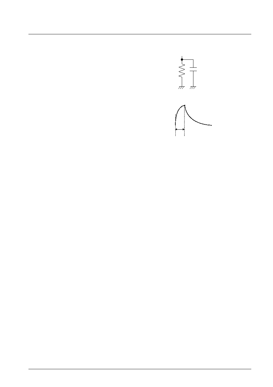
LA17000M
No. 6522-47/54
(9) About the noise canceller
The noise canceller improves the characteristics by implementing the circuits that determine the gate time with a
logic circuit.
Because a conventional noise canceller determines the time
constant according to CR as shown in Fig. 5, the rise time is
dependent on the CR, as shown in Fig. 6. This caused a delay
in the rise, which resulted in a deterioration of noise filtering
performance when the rise was delayed too much.
In the LA17000, the circuits that determine the gate time have
been configured with logic, resulting in a faster rise and
making more reliable noise filtering possible.
A13383
A13384
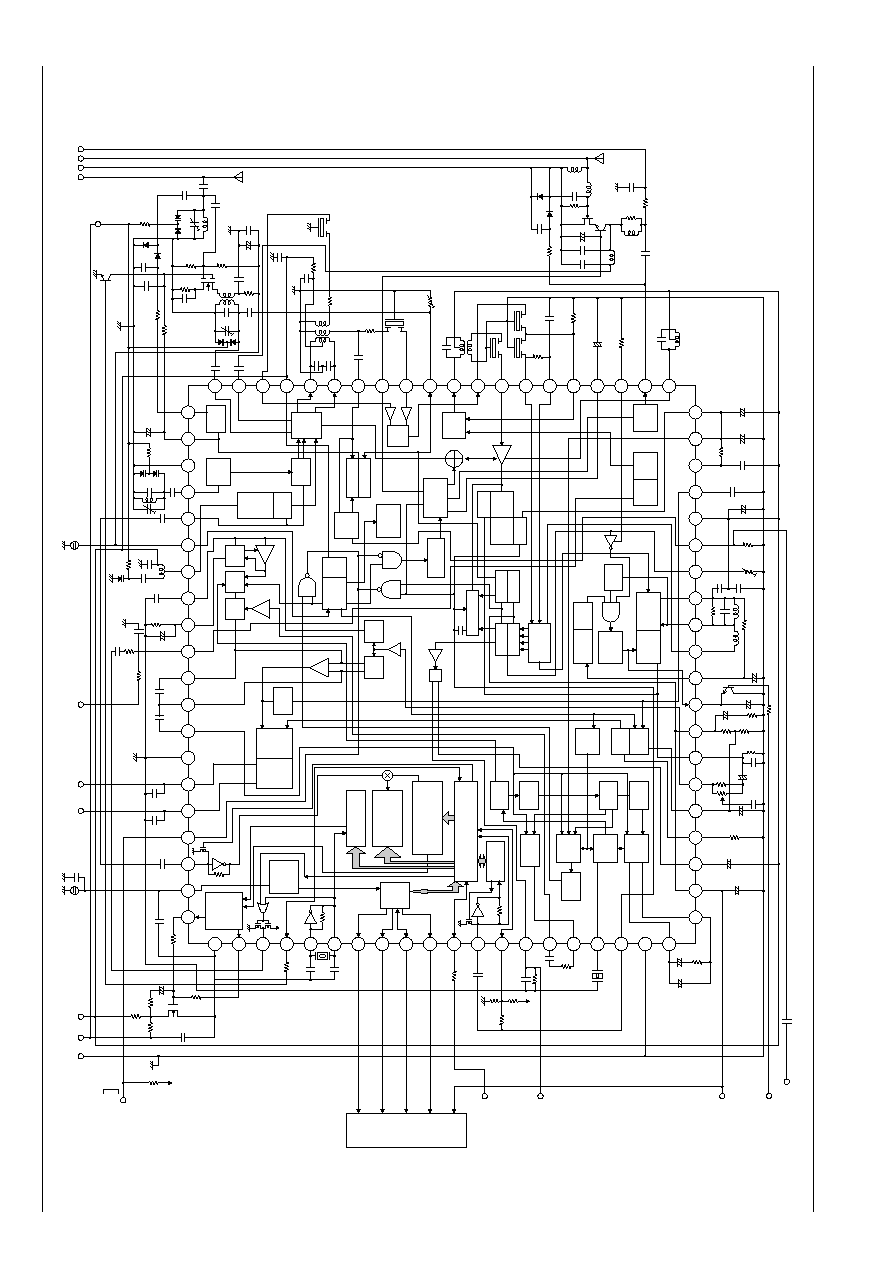
LA17000M
Block Diagram
No. 6522-48/54
1
FM
ANTD
ANT
D
2
FM RF
AGC
3
FE
GND
4
FM
OSC
5
6
AM/FM
SW
7
AM
OSC
8
NC
Sens
9
NC
AGC
10
AM
OSC
11
Gore
OUT
12
13
MPX
Pdot IN
14
NC MPX
GND
15
16
17
SD
ST-IND
18
PLL IN
19
20
PD1
41
AM/FM
S-METER
42
43
MRC
OUT
44
SNC
HCC
NC
45
46
47
DET
OUT
SEP
ADJ
48
FM
S-METER
49
MUTE
DRIVE
50
AFC
IN
51
QD
OUT
52
QD
IN
53
VREF
54
FM
SD
55
KEYED
AGC
56
VCC
57
C.
HCC
58
AM
LC
59
PILOT
DET
60
IF
AGC
21
PLL
VSS
22
PDS
23
XBUFF
24
I/O-2
25
X' IN
26
X' OUT
27
CE
28
DI
29
CL
30
DO
31
I/O-1
32
HCTR
33
SEEKSW
34
35
36
37
MPX VCO
38
IF COUNT BUFF
SEEK/STOP
switch
CSB912TF108
39
GND
40
PHASE
COMP
61
AM DET
62
AM ANTD
WIDE AGC
63
FM MUTE
ON ADJ
64
RF AGC
65
2nd MIX IN
66
FM IF BYPASS
VSM
SHIFTER
67
FM IF
IN
68
69
1st IF OUT
70
AM MIX OUT
71
AM SD ADJ
WIDE AGC IN
72
1st IF IN
73
AM RF AGC OUT
74
75
N-AGC IN
MUTE ATT ADJ
76
MIX OUT
77
FE VCC
78
1st IF
Narrow IN
79
AM 1st
MIX IN
80
FM
MIX IN
3.3
µ
F
0.022
µ
F
0.022
µ
F
0.01
µ
F
0.47
µ
F
1
µ
F
0.01
µ
F
0.022
µ
F
0.015
µ
F
6800pF
0.01
µ
F
30k
1M
350
51k
30k
10k
22k
51k
10k
11k
300
51k
470
100k
510
33
10k
10k
24k
30k
12k
62k
82k
560
56k
33k
33k
1000pF
10k
50k
5.6k
47k
47k
47k
100k
100k
51k
5V
10k
100k
10k
10pF
300pF
150pF
100pF
30pF
VCC=8V
FM ANT IN
5pF
AGC
HPH
HOLE
DET
F.F.19k
90
PHASE
COMP.
VCO
PILOT
DET.
CCB
I/F
POWER
ON
RESET
PHASE
DETECTOR
CHARGE
PUMP
F.F.19k
90
F.F.30k
0
F.F.
PILOT
CAN.
UNTVERSAL
COUNTER
DATA SHIFT REGISTER
LATCH
12Bits
PROGRAMMABLE
DIVIDER
SWALLOW
COUNTER
1/16,1/17 4Bits
REFERENCE
DIVIDER
TRIG
HCC
SNC
VCO
STOP
OC-C
DET
AFC
CI AMP
LPF
TRIG
GATE
+
--
MIX
MIX
ANT
D
OSC
BUFF
OSC
Q.DET
MUTE
AMP.
MUTE
DRIVE
DET
IF
AGC
L.C.
BUFF
OSC
BUFF
AM
1ST
OSC
BUFF
IF LIMIT
AMP.
Keyed
AGC
MAIN
HC
SUB
DEC
MAT
RIX
F.E
REG
FM/AM
SWICH
AM/FM
VREF
CF
SW
W.B AGC
RF AGC
AM SM
AM SD
FM SM
FM SD
IF BUFFER
MRC
RF AGC
WB AGC
TWEET
+
+
+
+
+
+
+
+
+
+
+
+
+
+
+
+
0.015
µ
F
0.22
µ
F
3.3
µ
F
15pF
15pF
0.022
µ
F
0.022
µ
F
100
µ
H
100
µ
H
0.022
µ
F
0.022
µ
F
47
µ
F
FC18
100
µ
H
1MH
0.022
µ
F
1
µ
F
0.022
µ
F
100
µ
F
+
2.2
µ
F
0.47
µ
F
1
µ
F
10
µ
F
0.22
µ
F
2200pF
0.1
µ
F
0.47
µ
F
0.01
µ
F
0.22
µ
F
1
µ
F
1
µ
F
0.22
µ
F
1
µ
F
0.47
µ
F
0.01
µ
F
0.022
µ
F
Pdot C
ADJ
100pF
5V
24pF
24pF
micro contlorrer
10.25
MHz
PLL VDD=5V
FM BF GND
L-CH
CF SW
R-CH
FMIF AMNC
MPX VCC
FM/AM
VT
FMIF AM
GND
SEEK
AM/FM SD
STOP
FM ST IND
SDSTSW
I/O-1
To
microcontroller
MUTE
OFF(RDS)
AM
(STEFEO)
IF OUT
MRC
SENOR
AUTO ADJ
+
30
200k
100
100k
100k
220
30k
15
30
100k
150
0.022
µ
F
5pF
0.022
µ
F
0.022
µ
F
0.1
µ
F
0.022
µ
F
100
µ
F
1000pF
1000pF
37pF
6pF
1000pF
8pF
1000pF
18pF
62pF
AM ANT IN
AM V
CC
A13385
LA17000M
No. 6522-49/54
Recommended External Components
Component name
Manufacturer
Component
Component model number
number
AM loading coil
Toko
L1
7TL-269ANS-0720Z
Sumida Electronics Co., Ltd.
SA-1062
AM ANT-IN
Toko
L2
7PSU-385BNS-027Z
Sumida Electronics Co., Ltd.
SA-1048
AM RF LPF
Toko
L3
5VUS-A286LBIS-15327
Sumida Electronics Co., Ltd.
SA-1051
AM choke coil
Toko
L4
8RB-187LY-222J
Sumida Electronics Co., Ltd.
RC875-222J
AM 2nd MIX coil
Toko
L7
5PG-5PGLC-5310N
Sumida Electronics Co., Ltd.
SA-264
AM IF coil
Toko
L8
7PSGTC-50002Y=S
Sumida Electronics Co., Ltd.
SA-1063/SA-1112
AM OSC1 coil
Toko
L9
7KSS-V666SNS-213BY
Sumida Electronics Co., Ltd.
SA-359
AM/FM MIX coil with
Toko
L10
7PSG-8261N-5202D=S
selectivity switch
AM/FM MIX coil
Sumida Electronics Co., Ltd.
L10
SA-266
without selectivity switch
Toko
371DH-1108FYH
FM detection coil
Sumida Electronics Co., Ltd.
L14
SA-208
Toko
DM600DEAS-8407GLF
FM OSC coil
Sumida Electronics Co., Ltd.
L11
SA-125 (JP), SA-278 (US)
Toko
T-666NF-251APZ (JP), T-666SNF-2471B (US)
FM RF coil
Sumida Electronics Co., Ltd.
L12
SA-143 (JP), SA-250 (US)
Toko
T-666NF-269X (JP), T-666SNF-246JA (US)
FM ANT coil
Sumida Electronics Co., Ltd.
L13
SA-144 (JP), SA-231 (US)
Toko
T-666NF-268Z (JP), T-666SNF-244X (US)
MPX ceramic oscillator
Murata Manufacturing Co., Ltd.
VCO1
CSB912JF108 (912 kHz)
Kyocera
KRB-912F108 (912kHz)
PLL X'tal oscillator
Nihon Dempa kogyo
VCO2
LN-P-0001 (10.25, 10.35 MHz)
FM ceramic filter
Murata Manufacturing Co., Ltd.
CF1
SFE 10.7MS3A50K-A
FM/AM narrow band
Murata Manufacturing Co., Ltd.
CF2
SFE 10.7 MTE
ceramic filter
AM ceramic filter
Toko
CF3
LFCM450H
Murata Manufacturing Co., Ltd.
SFPS450H
AM pin diode
SANYO Electric Co., Ltd.
PIN1
1SV234/267
AMRF FET+TR
SANYO Electric Co., Ltd.
FET1
FC18
AM OSC1 varactor
SANYO Electric Co., Ltd.
VD2
SVC252/253
FM pin diode
SANYO Electric Co., Ltd.
PIN2
1SV234
FM RF amplifier FET
SANYO Electric Co., Ltd.
FET2
3SK263/264
FM RF/ANT/OSC varactor
SANYO Electric Co., Ltd.
VD3
SVC231/208
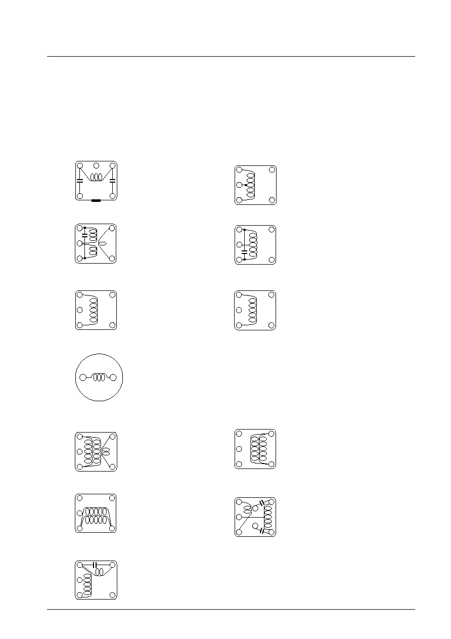
LA17000M
No. 6522-50/54
Crystal oscillator
Nihon Dempa Kogyo Co., Ltd.
Frequency:
10.25 MHz
10.35 MHz
CL:
16pF
16pF
Model name:
LN-P-0001
LN-P-0001
Coil specifications
Sumida Electronics Co., Ltd.
[AM block]
AM FILTER (SA-1051)
AM OSC (SA-359)
AM IF1 (SA-264)
AM IF2 (SA-1063)
AM loading (SA-1062)
AM ANT IN (SA-1048)
For AM RF amplifier (RC875-222J)
[FM block]
FM RF (SA-1060)
FM ANT (SA-1061)
FM OSC (SA-1052)
FM MIX (SA-266)
FM DET (SA-208)
3
2
4
1
6
S
3
2
4
1
6
S
1
2
3
6
4
3
2
4
1
6
S
3
2
4
1
6
S
0.12UEW
3
2
4
1
6
S
S
S
3
2
4
1
6
S
S
3
2
4
1
6
S
3
2
4
1
6
S
3
2
4
8
7
1
6
S
S
C1
C2
3
2
4
1
6
S
S
(without selectivity switch)
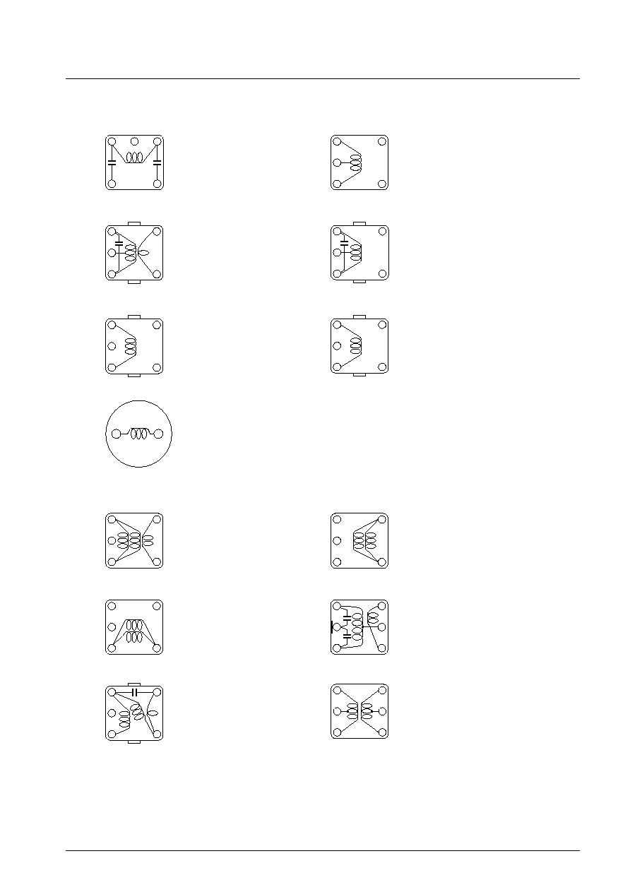
LA17000M
No. 6522-51/54
TOKO Co., Ltd.
[AM block]
AM FILTER (A286LBIS-15327)
AM OSC (V666SNS-213BY)
AM IF1 (7PSGTC-5001A=S)
AM IF2 (7PSGTC-5002Y=S)
AM loading (269ANS-0720Z)
AM ANT IN (385BNS-027Z)
For AM RF amplifier (187LY-222)
[FM block]
FM RF (V666SNS-208AQ)
FM ANT (V666SNS-209BS)
FM OSC (V666SNS-205APZ)
FM MIX (371DH-1108FYH)
FM DET (DM600DEAS-8407GLF)
FM MIX (826IN-5202D=S)
3
2
4
5
1
6
S
S
0.062UEW
3
2
4
1
6
0.072MUEW
3
2
5
4
1
6
S
S
0.07-2UEW
3
2
4
1
6
S
0.12-2UEW
3
2
4
1
6
S
0.1-2UEW
3
2
4
1
6
S
S
0.1-2UEW
0.12UEW
3
2
4
1
6
0.063UEW
3
2
4
1
6
0.053UEW
3
2
4
1
6
0.053UEW
3
2
4
1
6
0.053UEW
1
2
3
6
4
3
2
4
1
6
0.12UEW
(with selectivity switch)
External 82P2 in parallel (1-G, 3-G)
(without selectivity switch)
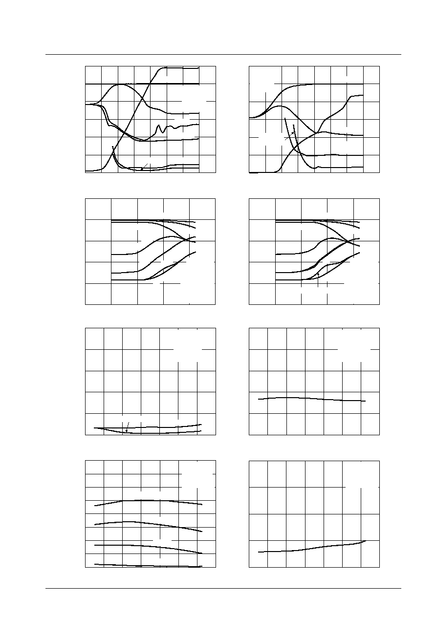
LA17000M
No. 6522-52/54
-80
-100
-60
-40
-20
0
20
-80
-100
-60
-40
-20
0
20
-20
0
20
40
60
80
100
120
140
-20
0
20
40
60
80
100
120
140
-60
-80
-40
-20
0
20
-60
-80
-40
-20
0
20
40
60
80
100
120
140
40
60
80
100
120
140
VSM
VSM
MOD ON
MOD ON
MOD OFF
MOD OFF
THD 100
THD 80
fm=400Hz
THD 30
fm=400Hz
THD 30
80dBSN
80dBSN
60dBSN
60dBSN
40dBSN
40dBSN
40dBIN
40dBIN
60dBIN
60dBIN
80dBIN
80dBIN
fud modu ON
fud modu ON
SEP
AMR
V
SM
, THD - V, %
V
SM
, THD - V, %
VCC=8.4V
fr=98.1MHz
fm=1kHz
dev=22.5kHz
VCC=8.5V
fD=1000kHz
fm=400Hz
modu=30
fuD=1040kHz
fm=1kHz ON/OFF
modu=30
VCC=8.5V
fD=1000kHz
fm=400Hz
modu=30
fuD=1400kHz
fm=1kHz ON/OFF
modu=30
VCC=8.4V
fr=1MHz
fm=1kHz
dev=30
1
0
2
3
4
5
-40
-20
0
20
40
60
80
100
20
0
40
60
80
100
-40
-20
0
20
40
60
80
100
-40
-20
0
20
40
60
80
100
1
0
2
3
4
5
6
7
8
-40
-20
0
20
40
60
80
100
20
0
40
60
80
dev=75kHz
VSM=60dB
40dB
20dB
-20dB
dev=22.5kHz
LS
L
S
- dB
VCC=8.4V
fr=98.1MHz
fm=1kHz
dev=kHz
ANT IN=80dB
VCC=8.4V
fr=98.1MHz
fm=1kHz
dev=22.5kHz
VCC=8.4V
fr=98.1MHz
fm=1kHz
dev=22.5kHz
VCC=8.4V
fr=98.1MHz
fm=1kHz
dev=22.5kHz
ANT IN=80dB
FM I/O Characteristics
AM I/O Characteristics
AF output, noise ≠ dB
AF output, noise ≠ dB
AF output, noise ≠ dB
AF output, noise ≠ dB
AM2 Signal Interference Characteristics
AM2 Signal Interference Characteristics
ANT input, IN ≠ dB
µ
ANT input, IN ≠ dB
µ
ANT input, IN ≠ dB
µ
ANT input, IN ≠ dB
µ
T
otal harmonic distortion,
THD ≠ %
S-meter voltage,
V
SM
--
V
FM Antenna input Temperature Characteristics (1)
FM Antenna input Temperature Characteristics (2)
Ambient temperature, Ta ≠ ∞C
Ambient temperature, Ta ≠ ∞C
Ambient temperature, Ta ≠ ∞C
Ambient temperature, Ta ≠ ∞C
Separation, Sep -- dB
FM Antenna input Temperature Characteristics (3)
FM Antenna input Temperature Characteristics (4)
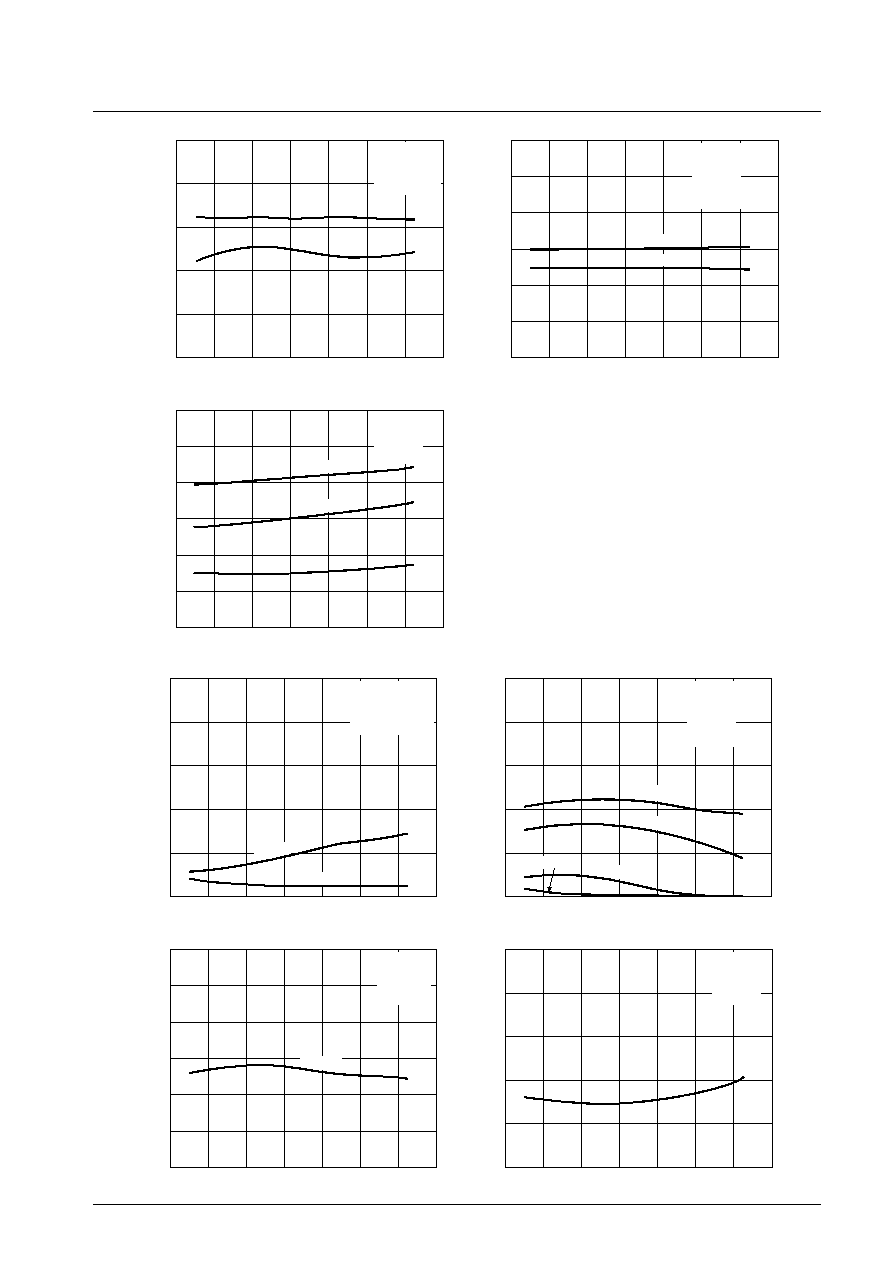
LA17000M
No. 6522-53/54
1
0
2
3
4
5
-40
-20
0
20
40
60
80
100
-40
-20
0
20
40
60
80
100
1
0
2
3
4
5
-40
-20
0
20
40
60
80
100
-40
-20
0
20
40
60
80
100
20
0
40
60
80
100
120
20
0
40
60
80
100
dev=80
dev=30
SD
VSM=60dB
40dB
20dB
-20dB
AGCFOM
AGCFOM - dB
VCC=8.4V
fr=1MHz
fm=400Hz
dev=30
ANT IN=80dB
VCC=8.4V
fr=1MHz
fm=400Hz
dev=30
VCC=8.4V
fr=1MHz
fm=400Hz
dev=30
VCC=8.4V
fr=1MHz
fm=400Hz
ANT IN=80dB
-40
-20
0
20
40
60
80
100
-40
-20
0
20
40
60
80
100
-40
-20
0
20
40
60
80
100
20
0
40
60
80
100
-60
-40
-80
-20
0
20
40
S/N
W-AGC
N-AGC
SD
AMR
S/N, AMR - dB
SD, W-AGC N-AGC
- dB
20
40
0
60
80
100
120
fm=1kHz
fm=10kHz
VCC=8.4V
fr=98.1MHz
fm=1kHz
dev=22.5kHz
ANT IN=80dB
VCC=8.4V
fr=98.1MHz
fm=1kHz
dev=22.5kHz
VCC=8.4V
fr=98.1MHz
fm=1kHz
dev=22.5kHz
FM Antenna input Temperature Characteristics (5)
FM Antenna input Temperature Characteristics (6)
Ambient temperature, Ta ≠ ∞C
Ambient temperature, Ta ≠ ∞C
Output voltage,
V
O
≠ dBm
Ambient temperature, Ta ≠ ∞C
FM Antenna input Temperature Characteristics (7)
AM Antenna input Temperature Characteristics (1)
AM Antenna input Temperature Characteristics (2)
T
otal harmonic distortion,
THD ≠ %
S-meter voltage,
V
SM
--
V
Ambient temperature, Ta ≠ ∞C
Ambient temperature, Ta ≠ ∞C
Ambient temperature, Ta ≠ ∞C
Ambient temperature, Ta ≠ ∞C
SD sensitivity
, SD ≠ dB
µ
AM Antenna input Temperature Characteristics (3)
AM Antenna input Temperature Characteristics (4)
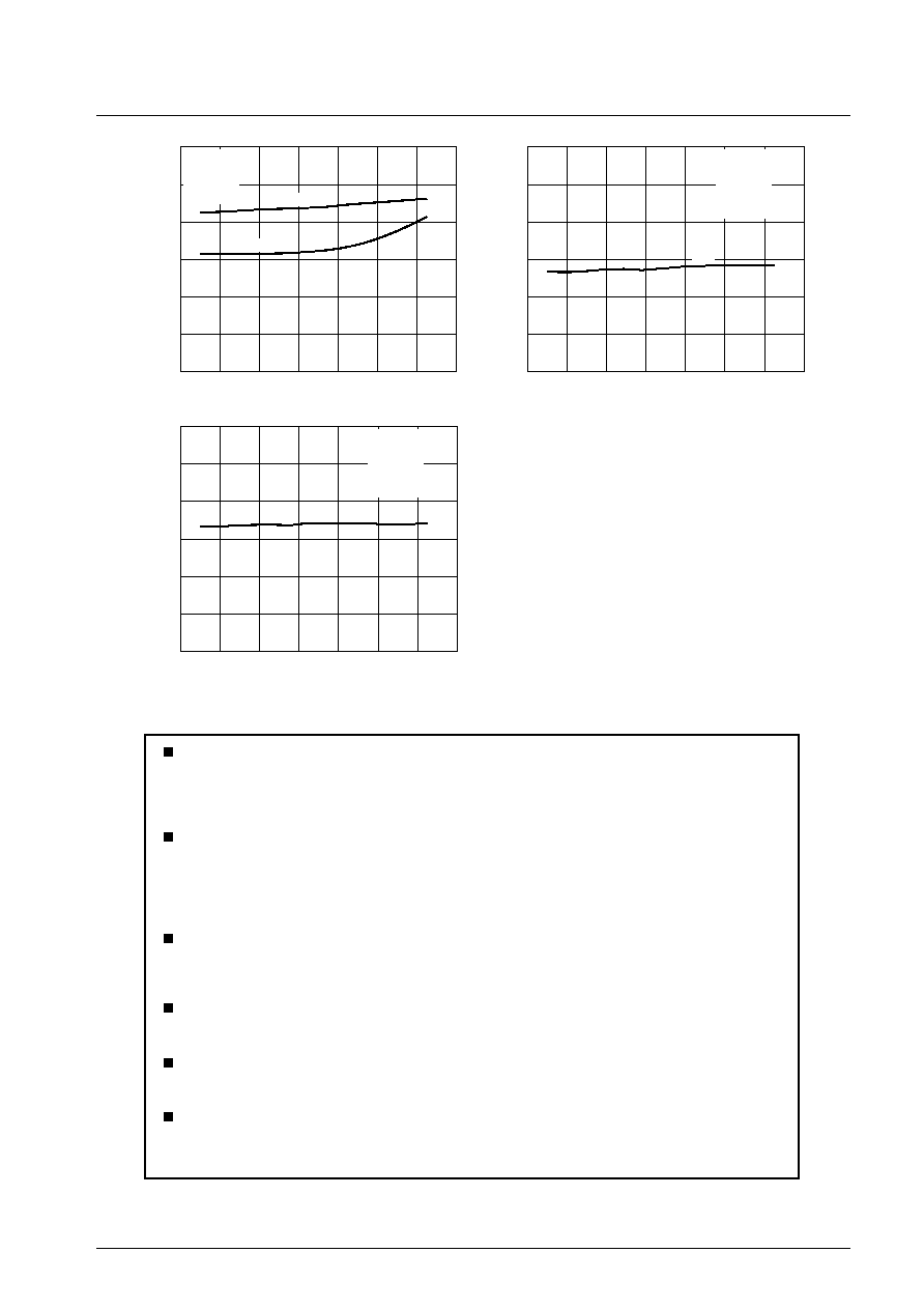
LA17000M
No. 6522-54/54
-40
-20
0
20
40
60
80
100
-40
-20
0
20
40
60
80
100
-40
-20
0
20
40
60
80
100
20
0
40
60
80
100
120
40
20
0
60
80
100
120
W-AGC
N-AGC
W-AGC, N-AGC - dB
S/N - dB
-40
-60
-80
-20
0
20
40
S/N
VO
VCC=8.4V
fr=1MHz
fm=400Hz
dev=30
ANT IN=80dB
VCC=8.4V
fr=1MHz
fm=400Hz
dev=30
ANT IN=80dB
VCC=8.4V
fr=1MHz
fm=400Hz
dev=30
AM Antenna input Temperature Characteristics (5)
AM Antenna input Temperature Characteristics (6)
AM Antenna input Temperature Characteristics (7)
Output voltage,
V
O
≠ dBm
Ambient temperature, Ta ≠ ∞C
Ambient temperature, Ta ≠ ∞C
Ambient temperature, Ta ≠ ∞C
Specifications of any and all SANYO products described or contained herein stipulate the performance,
characteristics, and functions of the described products in the independent state, and are not guarantees
of the performance, characteristics, and functions of the described products as mounted in the customer's
products or equipment. To verify symptoms and states that cannot be evaluated in an independent device,
the customer should always evaluate and test devices mounted in the customer's products or equipment.
SANYO Electric Co., Ltd. strives to supply high-quality high-reliability products. However, any and all
semiconductor products fail with some probability. It is possible that these probabilistic failures could
give rise to accidents or events that could endanger human lives, that could give rise to smoke or fire,
or that could cause damage to other property. When designing equipment, adopt safety measures so
that these kinds of accidents or events cannot occur. Such measures include but are not limited to protective
circuits and error prevention circuits for safe design, redundant design, and structural design.
In the event that any or all SANYO products (including technical data, services) described or contained
herein are controlled under any of applicable local export control laws and regulations, such products must
not be exported without obtaining the export license from the authorities concerned in accordance with the
above law.
No part of this publication may be reproduced or transmitted in any form or by any means, electronic or
mechanical, including photocopying and recording, or any information storage or retrieval system,
or otherwise, without the prior written permission of SANYO Electric Co., Ltd.
Any and all information described or contained herein are subject to change without notice due to
product/technology improvement, etc. When designing equipment, refer to the "Delivery Specification"
for the SANYO product that you intend to use.
Information (including circuit diagrams and circuit parameters) herein is for example only; it is not
guaranteed for volume production. SANYO believes information herein is accurate and reliable, but
no guarantees are made or implied regarding its use or any infringements of intellectual property rights
or other rights of third parties.
This catalog provides information as of June, 2001. Specifications and information herein are subject to
change without notice.