 | –≠–ª–µ–∫—Ç—Ä–æ–Ω–Ω—ã–π –∫–æ–º–ø–æ–Ω–µ–Ω—Ç: LA1780M | –°–∫–∞—á–∞—Ç—å:  PDF PDF  ZIP ZIP |

Any and all SANYO products described or contained herein do not have specifications that can handle
applications that require extremely high levels of reliability, such as life-support systems, aircraft's
control systems, or other applications whose failure can be reasonably expected to result in serious
physical and/or material damage. Consult with your SANYO representative nearest you before using
any SANYO products described or contained herein in such applications.
SANYO assumes no responsibility for equipment failures that result from using products at values that
exceed, even momentarily, rated values (such as maximum ratings, operating condition ranges, or other
parameters) listed in products specifications of any and all SANYO products described or contained
herein.
Overview
The LA1780M integrates all six blocks required in a car
radio tuner on a single chip. The LA1780M is based on
the LA1888NM, and features improvements to each of the
blocks; improvements designed to provide improved noise
characteristics, especially for noise related to multipath,
three-signal intermodulation distortion, and two-signal
suppression.
Functions
∑ FM front end
∑ FM IF
∑ Noise canceller
∑ Multiplex
∑ AM up-conversion
∑ FM/AM switch
∑ MRC
Features
∑ Improved noise reduction methods
-- The FM front end provides excellent 3-signal
characteristics equivalent to those of the LA1193M.
-- Superlative listenability due to improved medium and
weak field noise canceller characteristics.
-- Improved separation characteristics
-- Anti-birdie filter
-- Improved AM and FM thermal characteristics
-- Excellent FM signal meter linearity
-- Modified N.C. circuit for improved noise rejection
∑ Double conversion AM tuner (up conversion)
Reduces the number of external components required as
compared to earlier double conversion tuners, in
particular, no crystal is required (when used in
conjunction with the LC72144).
∑ Sample-to-sample variation reduction circuit built into
the FM IF circuit.
(Fixed resistors are used for the SD, keyed AGC, mute
on adjustment, ATT, SNC, and HCC functions.)
∑ Since the LA1780M retains the block structure of the
LA1888NM, products using that IC can be easily
converted, allowing further end product miniaturization.
Package Dimensions
Unit:mm
3159-QFP64E
Monolithic Linear IC
Ordering number : ENN5724A
33100TN (OT)/92498RM (OT) No. 5724-1/38
SANYO Electric Co.,Ltd. Semiconductor Company
TOKYO OFFICE Tokyo Bldg., 1-10, 1 Chome, Ueno, Taito-ku, TOKYO, 110-8534 JAPAN
Single-Chip Tuner IC for Car Radios
LA1780M
14.0
17.2
1.0
1.0
1.6
0.15
0.35
0.1
15.6
0.8
0.8
3.0max
1
16
17
32
33
48
49
64
2.7
14.0
17.2
1.0
1.0
1.6
0.8
Allowable power dissipation,
Pdmax -- mW
Ambient temperature, Ta -- ∞C
Mounted on a 40
◊
80
◊
1.3 mm
3
glass epoxy printed circuit board
Independent IC
SANYO: QFP64E (QIP64E)
[LA1780M]

Ratings
Parameter
Symbol
Conditions
min
typ
max
unit
[FM Characteristics] At the FM IF input
Current drain
I
CCO
-FM
No input,
I
40 +
I
45 +
I
54 +
I
59 +
I
60 +
I
61
60
94
110
mA
Demodulation output
V
O
-FM
10.7 MHz, 100dBµ, 1 kHz, 100%mod, The pin 15 output
205
310
415
mVrms
Pin 31 demodulation output
V
O
-FM31
10.7 MHz, 100dBµ, 1 kHz, 100%mod, The pin 31 output
190
295
380
mVrms
Channel balance
CB
The ratio between pins 15 and 16 at 10.7 MHz, 100 dBµ, 1 kHz
≠1
0
+1
dB
Total harmonic distortion
THD-FM mono
10.7 MHz, 100 dBµ, 1 kHz, 100% mod, pin 15
0.3
1
%
Signal-to-noise ratio: IF
S/N-FM IF
10.7 MHz, 100 dBµ, 1 kHz, 100% mod, pin 15
75
82
dB
AM suppression ratio: IF
AMR IF
10.7 MHz, 100 dBµ, 1 kHz, f
m
= 1 kHz, 30% AM, pin 15
55
68
dB
Att-1
10.7 MHz, 100 dBµ, 1 kHz. The pin 15
5
10
15
dB
attenuation when V33 goes from 0 to 2 V
Muting attenuation
Att-2
10.7 MHz, 100 dBµ, 1 kHz. The pin 15
15
20
25
dB
attenuation when V33 goes from 0 to 2 V
*
1
Att-3
10.7 MHz, 100 dBµ, 1 kHz. The pin 15
28
33
38
dB
attenuation when V33 goes from 0 to 2 V
*
2
Separation
Separation
10.7 MHz, 100 dBµ, L+R = 90%, pilot = 10%. The pin 15 output
30
40
dB
ratio
Stereo on level
ST-ON
The pilot modulation such that V26 < 0.5 V
1.2
2.4
4.4
%
Stereo off level
ST-OFF
The pilot modulation such that V26 > 3.5 V
0.6
1.6
%
Main total harmonic distortion
THD-Main L
10.7 MHz, 100 dBµ, L+R = 90%, pilot = 10%. The pin 15 signal
0.3
1.2
%
Pilot cancellation
PCAN
10.7 MHz, 100 dBµ, pilot = 10%.
20
30
dB
The pin 15 signal/the pilot level leakage. DIN audio
SNC output attenuation
AttSNC
10.7 MHz, 100 dBµ, L-R = 90%, pilot = 10%.
1
5
9
dB
V28 = 3 V
0.6 V, pin 15
AttHCC-1
10.7 MHz, 100 dBµ, 10 kHz, L+R = 90%, pilot = 10%.
0.5
4.5
8.5
dB
HCC output attenuation
V29 = 3 V
0.6 V, pin 15
AttHCC-2
10.7 MHz, 100 dBµ, 10 kHz, L+R = 90%,
6
10
14
dB
pilot = 10%. V29 = 3 V
0.1 V, pin 15
Input limiting voltage
Vi-lim
100 dBµ, 10.7 MHz, 30% modulation. The IF input such
33
40
47
dBµ
that the input reference output goes down by 3 dB
Muting sensitivity
Vi-mute
The IF input level (unmodulated) when V33 = 2 V
27
35
43
dBµ
SD-sen1 FM
The IF input level (unmodulated) (over 100 mV rms)
54
62
70
dBµ
SD sensitivity
such that the IF counter buffer output goes on
SD-sen2 FM
54
62
70
dBµ
IF counter buffer output
V
IFBUFF-FM
10.7 MHz, 100 dBµ, unmodulated. The pin 23 output
220
330
440
mVrms
V
SM
FM-1
No input. The pin 24 DC output, unmodulated
0.0
0.1
0.3
V
Signal meter output
V
SM
FM-2
50 dBµ. The pin 24 DC output, unmodulated
0.4
1.0
1.5
V
V
SM
FM-3
70 dBµ. The pin 24 DC output, unmodulated
2.0
2.7
3.5
V
V
SM
FM-4
100 dBµ. The pin 24 DC output, unmodulated
4.7
5.5
6.2
V
Muting bandwidth
BW-mute
100 dBµ. The bandwidth when V33 = 2 V, unmodulated
100
150
200
kHz
Mute drive output
V
MUTE-100
100 dBµ, 0 dBµ. The pin 33 DC output, unmodulated
0.00
0.03
0.20
V
Operating Characteristics
at Ta = 25∞C, V
CC
= 8.0V, in the specified test cricuit for the FM IF input
Continued on next page.
No. 5724-2/38
LA1780M
Specifications
Maximum Ratings
at Ta = 25∞C
Operating Conditions
at Ta = 25∞C
Parameter
Symbol
Conditions
Ratings
Unit
Maximum supply voltage
V
CC
1 max
Pins 6, 40, and 61
9
V
V
CC
2 max
Pins 7, 45, 54, 59, and 60
12
V
Allowable power dissipation
Pd max
Ta
55∞C
950
mW
Operating temperature
Topr
≠40 to +85
∞C
Storage temperature
Tstg
≠40 to +150
∞C
Parameter
Symbol
Conditions
Ratings
Unit
Recommended supply voltage
V
CC
Pins 6, 7, 40, 45, 54, 59, 60, and 61
8
V
V
CC
ST IND
Pin 26
5 V
Operating supply voltage range
V
CC
op
7.5 to 9.0
V

Ratings
Parameter
Symbol
Conditions
min
typ
max
unit
[FM FE Mixer Input
N-AGC on input
V
N
-AGC
83 MHz, unmodulated.
80
87
94
dBµ
The input such that the pin 2 voltage is 2.0 V or below
W-AGC on input
V
W
AGC
83 MHz, unmodulated. The input such that the pin 2
100
106
112
dBµ
voltage is 2.0 V or below. (When the keyed AGC is set to 4.0 V.)
Conversion gain
A.V
83 MHz, 80 dBµ, unmodulated. The FE CF output
19
30
48
mVrms
Oscillator buffer output
V
OSCBUFFFM
No input
260
370
480
mVrms
[NC Block] NC input (pin 30)
Gate time
GATE1
f = 1 kHz, for a 1-µs, 100-mV p-o pulse
55
µs
Noise sensitivity
SN
The level of a 1 = kHz, 1-µs pulse input that starts
40
mVp-o
noise canceller operation. Measured at pin 30.
The pulse rejection effect provided by the noise canceller.
NC effect
SN-NC
For a repeated 1-µs wide pulse, frequency = 10 kHz,
5
150 mV p-o. The ratio of the FM mode pin 15 output
referenced to the AM mode pin 15 output (effective value)
[Multipath Rejection Circuit] MRC input (pin 27)
MRC output
VMRC
V24 = 5 V
2.2
2.3
2.4
V
MRC operating level
MRC-ON
The pin 32 input level at f = 70 kHz such that
10
15
20
mVrms
pin 24 goes to 5 V and pin 27 goes to 2 V
[AM Characteristics] AM ANT input
Practical sensitivity
S/N-30
1 MHz, 30 dBµ, f
m
= 1 kHz, 30% modulation, pin 15
20
dB
Detector output
V
O
-AM
1 MHz, 74 dBµ, f
m
= 1 kHz, 30% modulation, pin 15
85
120
170
mVrms
Pin 31 detector output
V
O
-AM31
1 MHz, 74 dBµ, f
m
= 1 kHz, 30% modulation, pin 31
75
110
150
mVms
AGC F.O.M.
V
AGC-FOM
1 MHz, 74 dBµ, referenced to the output, the input amplitude
56
61
66
dB
such that the output falls by 10 dB. Pin 15
Signal-to-noise ratio
S/N-AM
1 MHz, 74 dBµ, f
m
= 1 kHz, 30% modulation
47
52
dB
Total harmonic distortion
THD-AM
1 MHz, 74 dBµ, f
m
= 1 kHz, 80% modulation
0.3
1
%
Signal meter output
V
SM
AM-1
No input
0.0
0.2
0.5
V
V
SM
AM-2
1 MHz, 130 dBµ, unmodulated
3.8
4.8
6.2
V
Oscillator buffer output
V
OSCBUFF AM1
No input, the pin 5 output
185
230
mVrms
Wide band AGC sensitivity
W-AGCsen1
1.4 MHz, the input when V46 = 0.7 V
83
89
95
dBµ
W-AGCsen2
1.4 MHz, the input when V46 = 0.7 V (seek mode)
74
80
86
dBµ
SD sensitivity
SD-sen1 AM
1 MHz, the ANT input level such that the IF counter output turns on.
26
32
38
dBµ
SD-sen2 AM
1 MHz, the ANT input level such that the SD pin goes to the on state.
26
32
38
dBµ
IF buffer output
V
IFBUFF-AM
1 MHz, 74 dBµ, unmodulated. The pin 23 output
200
290
mVrms
No. 5724-3/38
LA1780M
Note: These measurements must be made using the either the IC-51-0644-824 or KS8277 IC socket (manufactured by Yamaichi Electronics).
*
1. When the resistor between pin 58 and ground is 200 k
.
*
2. When the resistor between pin 58 and ground is 30 k
.
Continued from preceding page.

No. 5724-4/38
LA1780M
Parameter
Symbol
Switch states
SW1
SW2
SW3
SW4
SW5
SW6
SW7
SW8
SW9
SW10
Current drain
I
CCO
-FM
ON
b
OFF
b
--
ON
OFF
OFF
ON
--
Demodulation output
V
O
-FM
ON
b
OFF
b
--
ON
OFF
OFF
ON
--
Pin 31 demodulation output
V
O
-FM31
ON
b
OFF
b
--
ON
OFF
OFF
ON
--
Channel balance
CB
ON
b
OFF
b
--
ON
OFF
OFF
ON
--
Total harmonic distortion
THD-FMmono
ON
b
OFF
b
--
ON
OFF
OFF
ON
--
Signal-to-noise ratio: IF
S/N-FM IF
ON
b
OFF
b
--
ON
OFF
OFF
ON
--
AM suppression ratio: IF
AMR IF
ON
b
OFF
b
--
ON
OFF
OFF
ON
--
Muting attenuation 1
Att-1
ON
b
OFF
b
--
ON
OFF
OFF
ON
--
Muting attenuation 2
Att-2
ON
b
OFF
b
--
ON
OFF
OFF
ON
--
Muting attenuation 3
Att-3
ON
b
OFF
b
--
ON
OFF
OFF
ON
--
Separation
Separation
ON
b
OFF
b
--
ON
OFF
OFF
ON
--
Stereo on level
ST-ON
ON
b
OFF
b
--
ON
OFF
OFF
ON
--
Stereo off level
ST-OFF
ON
b
OFF
b
--
ON
OFF
OFF
ON
--
Main total harmonic distortion
THD-Main L
ON
b
OFF
b
--
ON
OFF
OFF
ON
--
Pilot cancellation
PCAN
ON
b
OFF
b
--
ON
OFF
OFF
OFF/ON
--
SNC output attenuation
AttSNC
ON
b
OFF
b
--
ON
OFF
OFF
ON
--
HCC output attenuation 1
AttHCC-1
ON
b
OFF
b
--
ON
OFF
OFF
ON
--
HCC output attenuation 2
AttHCC-2
ON
b
OFF
b
--
ON
OFF
OFF
ON
--
Input limiting voltage
Vi-lim
ON
b
OFF
b
--
ON
OFF
OFF
ON
ON
Muting sensitivity
Vi-mute
ON
b
OFF
b
--
ON
OFF
OFF
ON
--
SD sensitivity 1
SD-sen1 FM
ON
b
OFF
b
OFF
OFF
OFF
OFF
ON
--
SD sensitivity 2
SD-sen2 FM
ON
b
OFF
b
ON
OFF
OFF
OFF
ON
--
IF counter buffer output
V
IFBUFF-FM
ON
b
OFF
b
OFF
OFF
OFF
OFF
ON
--
Signal meter output 1
V
SM
FM-1
ON
b
OFF
b
--
ON
OFF
OFF
ON
--
Signal meter output 2
V
SM
FM-2
ON
b
OFF
b
--
ON
OFF
OFF
ON
--
Signal meter output 3
V
SM
FM-3
ON
b
OFF
b
--
ON
OFF
OFF
ON
--
Signal meter output 4
V
SM
FM-4
ON
b
OFF
b
--
ON
OFF
OFF
ON
--
Muting bandwidth
BW-mute
ON
b
OFF
b
--
ON
OFF
OFF
ON
--
Mute drive output
V
MUTE-100
ON
b
OFF
b
--
ON
OFF
OFF
ON
--
N-AGC on input
V
NAGC
ON
a
ON
b
--
ON
OFF
OFF
--
--
W-AGC on input
V
WAGC
ON
a
ON
b
--
ON
OFF
OFF
--
--
Conversion gain
A.V
ON
a
ON
b
--
ON
OFF
OFF
--
--
Oscillator buffer output
V
OSCBUFFFM
ON
a
ON
b
--
ON
OFF
OFF
--
--
Gate time 1
GATE1
ON
--
OFF
a
--
ON
OFF
OFF
--
--
Noise sensitivity
SN
ON
--
OFF
a
--
ON
OFF
OFF
--
--
NC effect
SN-NC
ON/OFF
--
OFF
a
--
ON
OFF
OFF
--
--
MRC output
V
MRC
ON
--
OFF
b
--
ON
OFF
OFF
--
--
MRC operating level
MRC-ON
ON
--
OFF
b
--
ON
OFF
OFF
--
--
Practical sensitivity
S/N-30
OFF
--
OFF
b
ON
ON
--
--
--
--
Detection output
V
O
-AM
OFF
--
OFF
b
ON
ON
--
--
--
--
Pin 31 detection output
V
O
-AM31
OFF
--
OFF
b
ON
ON
--
--
--
--
AGC F.O.M.
V
AGC-FOM
OFF
--
OFF
b
ON
ON
--
--
--
--
Signal-to-noise ratio
S/N-AM
OFF
--
OFF
b
ON
ON
--
--
--
--
Total harmonic distortion
THD-AM
OFF
--
OFF
b
ON
ON
--
--
--
--
Signal meter output 1
V
SM
AM-1
OFF
--
OFF
b
ON
ON
--
--
--
--
Signal meter output 2
V
SM
AM-2
OFF
--
OFF
b
ON
ON
--
--
--
--
Oscillator buffer output
V
OSCBUFF AM-1
OFF
--
OFF
b
ON
ON
--
--
--
--
Wide band AGC sensitivity 1
W-AGCsen 1
OFF
--
OFF
b
ON
ON
--
--
--
--
Wide band AGC sensitivity 2
W-AGCsen 2
OFF
--
OFF
b
ON
ON
--
--
--
--
SD sensitivity 1
SD-sen1 AM
OFF
--
OFF
b
OFF
OFF
--
--
--
--
SD sensitivity 2
SD-sen2 AM
OFF
--
OFF
b
OFF
OFF
--
--
--
--
IF buffer output
V
IFBUFF-AM
OFF
--
OFF
b
OFF
OFF
--
--
--
--
Test Conditions

Block Diagram
No. 5724-5/38
LA1780M
IF limiter
amplifier

Function List
FM Front End (Equivalent to the Sanyo LA1193)
∑ Double input type double balanced mixer
∑ Pin diode drive AGC output
∑ MOSFET second gate drive AGC output
∑ Keyed AGC adjustment pin
∑ Differential IF amplifier
∑ Wide band AGC sensitivity setting pin, and narrow
band AGC sensitivity setting pin
∑ Local oscillator
FM IF
∑ IF limiter amplifier
∑ S-meter output (also used for AM) 6-stage pickup
∑ Multipath detection pin (shared FM signal meter)
∑ Quadrature detection
∑ AF preamplifier
∑ AGC output
∑ Band muting
∑ Weak input muting
∑ Soft muting adjustment pin
∑ Muting attenuation adjustment pin
∑ IF counter buffer output (also used for AM)
∑ SD (IF counter buffer on level) adjustment pin
∑ SD output (active high) (also used for AM)
Noise Canceller
∑ High-pass filter (first order)
∑ Delay circuit based low-pass filter (fourth order)
∑ Noise AGC
∑ Pilot signal compensation circuit
∑ Noise sensitivity setting pin
∑ Function for disabling the noise canceller in AM
mode
Multiplex Functions
∑ Adjustment-free VCO circuit
∑ Level follower type pilot canceller circuit
∑ HCC (high cut control)
∑ Automatic stereo/mono switching
∑ VCO oscillation stop function (AM mode)
∑ Forced monaural
∑ SNC (stereo noise controller)
∑ Stereo display pin
∑ Anti-birdie filter
AM
∑ Double balanced mixer (1st, 2nd)
∑ IF amplifier
∑ Detection
∑ RF AGC (narrow/wide)
∑ Pin diode drive pin
∑ IF AGC
∑ Signal meter output (also used for FM)
∑ Local oscillator circuits (first and second)
∑ Local oscillator buffer output
∑ IF counter buffer output (also used by the FM IF)
∑ SD (IF counter buffer on level) adjustment pin
∑ SD output (active high) (also used for AM)
∑ Wide AGC
∑ Detection output frequency characteristics
adjustment pin (low cut, high deemphasis)
∑ AM stereo buffer
MRC (multipath noise rejection circuit)
AM/FM switching output (linked to the FM V
CC
)
No. 5724-6/38
LA1780M

Pin No.
Function
Description
Equivalent circuit
3
F.E.GND
Pin Descriptions
No. 5724-7/38
LA1780M
62 pin
An antenna damping current flows
1
Antenna damping drive
when the RF AGC voltage (pin 2)
reaches V
CC
-V
D
.
2
RF AGC
Used to control the FET
second gate.
Oscillator connection
4
OSC
The transistor and capacitors
required for the oscillator circuit
are integrated on the chip.
AM first oscillator
7
AM OSC
This circuit can oscillator up to the
SW band.
An ALC circuit is included.
Continued on next page.

No. 5724-8/38
LA1780M
Pin No.
Function
Description
Equivalent circuit
13
Pilot input
Pin 13 is the PLL circuit input pin.
14
N.C, MPX, MRC, GND
Ground for the N.C., MPX, and
MRC circuits.
After setting up the medium field
(about 50 dBµ) sensitivity with the
8
Noise AGC sensitivity
noise sensitivity setting pin (pin 8),
9
AGC adjustment
set the weak field (about 20 to
30 dBµ) sensitivity with the AGC
adjustment pin (pin 9)
11
Memory circuit connection
Recording circuit used during
12
Memory circuit connection
noise canceller operation.
Continued from preceding page.
Continued on next page.
Differential
amp
Gate
circuit
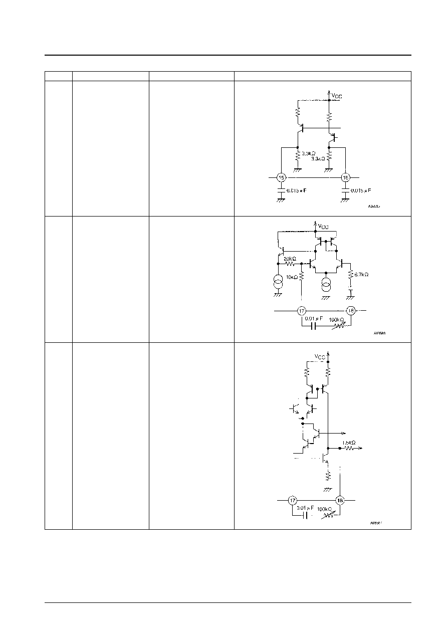
No. 5724-9/38
LA1780M
Pin No.
Function
Description
Equivalent circuit
15
MPX output (left)
Deemphasis
16
MPX output (right)
50 µs: 0.015 µF
75 µs: 0.022 µF
Adjustment is required since the
pilot signal level varies with the
17
Pilot canceller signal output
sample-to-sample variations in
the IF output level and other
parameters.
18
Pilot canceller signal output
Pin 18 is the output pin for the
pilot canceller signal.
Continued from preceding page.
Continued on next page.

No. 5724-10/38
LA1780M
Pin No.
Function
Description
Equivalent circuit
20
VCO
The oscillator frequency is 912 Hz.
KBR-912F108
(Kyocera Corporation)
CSB-912JF108
(Murata Mfg. Co., Ltd.)
Composite
signal
Use a trimmer to adjust the
19
Separation
subdecoder input level.
adjustment pin
(The output level is not modified in
mono and main modes.)
21
PHASE COMP.
22
PHASE COMP.
Continued from preceding page.
Continued on next page.

No. 5724-11/38
LA1780M
Pin No.
Function
Description
Equivalent circuit
Forced
SD: 2.5 V
SD circuit
IF counter
buffer
FM
S-meter
AM
S-meter
Outputs a 1-mA
current during AM
reception
Stereo
indicator
Seek/stop
switching
Continued from preceding page.
Continued on next page.
This pin functions both as the IF
counter buffer (AC output) and as
the seek/stop switch pin.
The voltage V23 switches
between the following three
modes.
23
IF counter buffer seek/stop
During FM reception:
switching
5 V:
Seek mode
2.5 V: Forced SD mode
0 V:
Reception mode
AM reception
(two modes: 0 and 5 V)
5 V:
Seek mode
0 V:
Reception mode
24
AM/FM signal meter
Fixed-current drive signal meter
output
In AM mode, pin 32 outputs a
32
Dedicated FM signal meter
1-mA current. Thus the HCC
circuit is turned off.
FM reception: the voltage V23
switches between three modes
as follows.
5 V:
The SD pin operates linked
to the IF counter buffer.
26
Stereo indicator for the SD pin
2.5 V: Forced SD mode: operates
as the SD pin.
0 V:
Reception mode: stereo
indicator
AM reception: (two modes: 0 and 5 V)
5 V:
Operates as the seek SD pin.
0 V:
Reception mode. Not used.
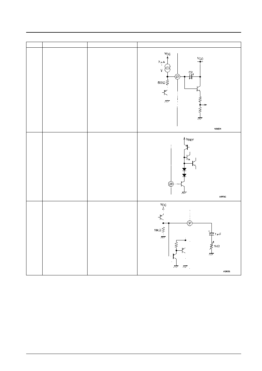
No. 5724-12/38
LA1780M
Pin No.
Function
Description
Equivalent circuit
Pin 28
Continued from preceding page.
Continued on next page.
The MRC detector time constant
27
MRC control voltage time
is determined by a 1-k
resistor
constant
and C2 when discharging and by
the 7-µA current and C2 when
charging.
28
SNC control input
The sub-output is controlled by a
0 to 1-V input.
The high band frequency output is
controlled by a 0 to 1-V input.
It can also be controlled by the
29
HCC control input
MRC output.
Use a resistor of at least 100 k
when controlling with the pin 32
FM S-meter signal.
MRC input
No. 5724-13/38
LA1780M
Pin No.
Function
Description
Equivalent circuit
SD circuit
FM
detector
output
AM
detector
Noise
canceller
MRC input
Band
muting
Continued from preceding page.
Continued on next page.
30
Noise canceller input
Pin 30 is the noise canceller input.
The input impedance is 50 k
.
Pin 31 is the AM and FM detector
output
In FM mode, this is a low-
impedance output.
31
AM/FM detector output
In AM mode, the output
impedance is 10 k
.
To improve the low band
separation, use a coupling
capacitor of over 10 µF.
FM S-meter output block
32
IF S-meter output and MRC
MRC AC input block
DC input
Adjust the external 1-k
resistor
to attenuate the MRC AC input
and control the circuit.
∑The muting time constant is
determined by an external RC
circuit as described below.
Attack time: T
A
= 10 k
◊
C1
Release time: T
R
= 50 k
◊
C1
∑Noise convergence adjustment
33
Mute drive output
The noise convergence can be
adjusted when there is no input
signal by inserting a resistor
between pin 33 and ground.
∑Muting off function
Ground pin 33 through a 4-k
resistor.
No. 5724-14/38
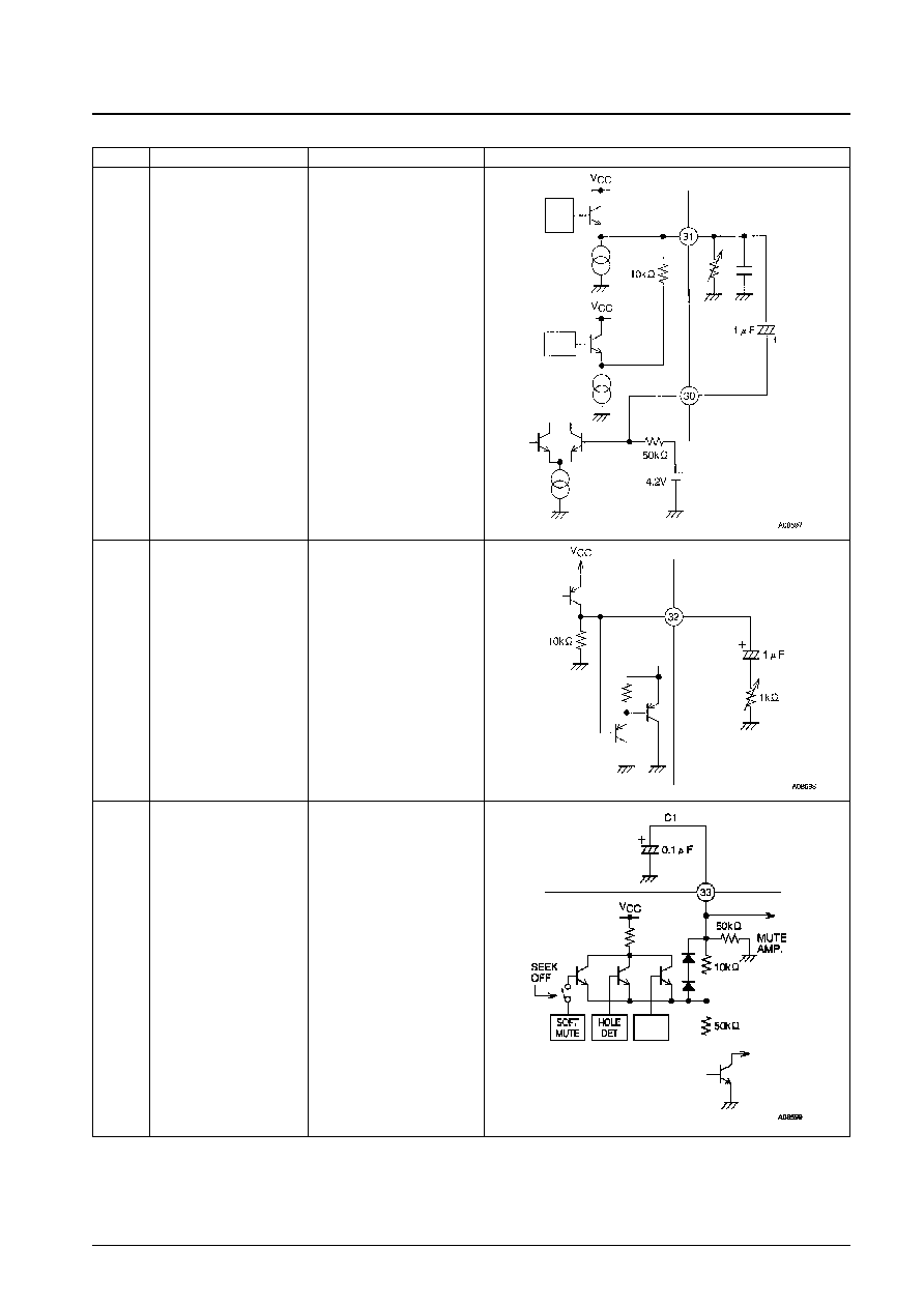
LA1780M
Pin No.
Function
Description
Equivalent circuit
Comparator
Quadrature
detector
IF limiter amplifier
Band
muting
Comparator
S-meter
S-meter
Continued from preceding page.
Continued on next page.
∑The resistor R
1
determines the
width of the band muting function.
Increasing the value of R
1
narrows the band.
Reducing the value of R
1
widens
the band.
34
AGC
35
QD output
∑Null voltage
36
QD input
When tuned, the voltage between
37
V
REF
pins 34 and 37, V
34 ≠ 37
, will be 0 V.
The band muting function turns
on when |V
34 ≠ 37
|
0.7 V.
V
37
= 4.9 V
A 130-µA current flows from pin
38
FM SD ADJ
38 and, in conjunction with the
external resistance R, determines
the comparison voltage.
The keyed AGC operates when
the voltage created by dividing the
pin 24 S-meter output voltage by
the 6.4 and 3.6 k
resistors
39
Keyed AGC
becomes lower than the voltage
AM stereo buffer
determined by the resistor
between pin 39 and ground.
This pin also is used as the AM
stereo IF buffer pin.

No. 5724-15/38
LA1780M
Pin No.
Function
Description
Equivalent circuit
Continued from preceding page.
Continued on next page.
The HCC frequency characteristics
41
HCC capacitor
are determined by the external
capacitor connected at this pin.
This pin is used to change the
frequency characteristics of the
unneeded audio band under
100 Hz in AM mode to produce
a clear audio signal.
Note: The LC capacitor must be
connected between this pin
and V
CC
(pin 40).
42
AM L.C. pin
This is because the detector
circuit operates referenced
to V
CC
.
The cutoff frequency f
C
is
determined by the following
formula.
f
C
= 1/2
◊
50 k
◊
C
Inserting a 1-M
resistor between
43
Pilot detector
pin 43 and V
CC
will force the IC
to mono mode.

No. 5724-16/38
LA1780M
Pin No.
Function
Description
Equivalent circuit
45
IF output
The IF amplifier load
Pin 40 V
CC
Pin 40 V
CC
Continued from preceding page.
Continued on next page.
Q1: Used for time constant
switching during seeks.
= 2.2 µF
◊
300 k
∑ Seek
44
IF AGC
= 2.2 µ
◊
10
The external capacitors are
connected to V
CC
.
This is because the IF amplifier
operates referenced to V
CC
.
AM antenna damping
I
46 = 6 mA (maximum)
46
drive output
This is the antenna damping
Wide band AGC input
current.

No. 5724-17/38
LA1780M
Pin No.
Function
Description
Equivalent circuit
52
IF input
The input impedance is 2 k
.
Antenna
damping
Inverter
Pin 24
For AGC
use
Continued from preceding page.
Continued on next page.
FM muting on level
Modify the value of the external
47
adjustment
resistor to adjust the muting on
level.
RF AGC rectification capacitor
The low frequency distortion is
determined as follows:
Increasing C48 and C57 improves
48
RF AGC bypass
the distortion but makes the
57
RF AGC
response slower.
Reducing C48 and C57
aggravates the distortion but
makes the response faster.
50
IF bypass
51
FM IF input
Due to the high gain of the limiter
amplifer, care must be taken when
choosing the grounding point for
the limiter amplifer input capacitor
to prevent oscillation.

No. 5724-18/38
LA1780M
Pin No.
Function
Description
Equivalent circuit
Pin 40 V
CC
Pin 40 V
CC
Pin 62
V
CC
Continued from preceding page.
Continued on next page.
∑ Input and output pin or the first
IF amplifier
∑ Inverting amplifier
53
IF amplifier output
V56 = 2 V
56
IF amplifier input
Input impedance: R
IN
= 330
V53 = 5.3 V
Output impedance
R
OUT
= 330
The mixer coil connected to the
54
Mixer output: 130 µA
pin 54 mixer output must be
49
Mixer input
wired to V
CC
(pin 40).
The pin 49 mixer input
impedance is 330
Pins 55 and 58 include built-in
DC cut capacitors.
The AGC on level is determined
by the values of the capacitors
C1 and C2.
55
W-AGC IN
Pin 55 functions as the SD
AM SD ADJ
sensitivity adjustment pin in
AM mode.
58
N-AGC IN
Muting attenuation
The output current I55 is 50 µA,
adjustment pin
and V55 varies depending on the
value of the external resistor.
The SD function operates by
comparing V55 with the S-meter
voltage.
Signal meter

No. 5724-19/38
LA1780M
Pin No.
Function
Description
Equivalent circuit
AM/FM
switching circuit
To RF
Amp.
To 2nd
MIX
Continued from preceding page.
Continued on next page.
Double balanced mixer
Pins 60 and 61 are the mixer
10.7-MHz output
Pins 63 and 64 are the mixer
input.
59
Mixer output
This is an emitter insertion type
60
circuit, and the amount of
63
Mixer input
insertion is determined by the
64
capacitors C1 and C2.
Note:The lines for pins 63 and 64
must be kept separated from
the lines for pins 60 and 61.
Pin 62 functions both as the FM
front end V
CC
and the AM/FM
switching circuit.
6
Front end V
CC
AM/FM
switching
1st MIX
First mixer input
62
INPUT
The input impedance is about
10 k
.
Crystal oscillator circuit
10
AM 2nd OSC
The Kinseki, Ltd. HC-49/U-S and
a C
L
of 20 pF must be used.
V6 voltage
Mode
When 8 V
FM
OPEN
AM

Usage Notes
1. Notes on V
CC
and Ground
2. Notes on AM Coil Connection
The V
CC
used for the first oscillator coil connected to pin 7 must be at the same potential as pin 61.
Connect to the IFT connected with pin 45, and to the MIX coil connected with pin 54. V
CC
must be at the same
potential as pin 40.
3. AM/FM Switching
Pin 6 is also used as the FM front end and RF AGC V
CC
4. Relationship between Pin 23 and Pin 26
∑ FM mode
Pin 26 functions as both the stereo indicator and the SD pin.
Pin 23: DC-input seek/stop pin (control pin)
AC output IF counter buffer pin
The Pin 23 Control Function and the Relationship between Pin 23 and Pin 26
No. 5724-20/38
LA1780M
Pin 40
V
CC
for the FM IF, AM, NC, MPX, and MRC blocks
Pin 25
Ground for the FM IF and AM blocks
Pin 14
Ground for the NC, MPX, and MRC blocks
Pin 61
V
CC
for the FM front end, AM first mixer, and first oscillator blocks
*
Pin 6
V
CC
for the FM front end and AGC blocks, and the AM/FM switching pin
Pin 3
Ground for the FM front end, first mixer, and first oscillator blocks
Pin 6 voltage
Mode
8
FM
OPEN
AM
Between 0 and a few
thousand Ohms.
IF counter buffer
SW1
SW2
Pin 23 voltage
Pin 26
Pin 26
OPEN
OPEN
5 V
IF counter buffer on
SD
ON
OPEN
2.5 V
OFF
High-speed SD
--
ON
Under 0.7 V
OFF
Stereo indicator
No. 5724-21/38
LA1780M
Used as RDS and similar function
SD detection by switching this mode.
Larger
R
38
Smaller R
38
S-meter
V
33
0.7 V or
over
On and
function-
ing as
SD
IF
counter
buffer
on
V
33
0.7 V or
over
Stereo
Mono
IF counter output off
Notes on FM SD
Band
muting
Mute drive
output
S-meter
IF counter buffer
IF counter output
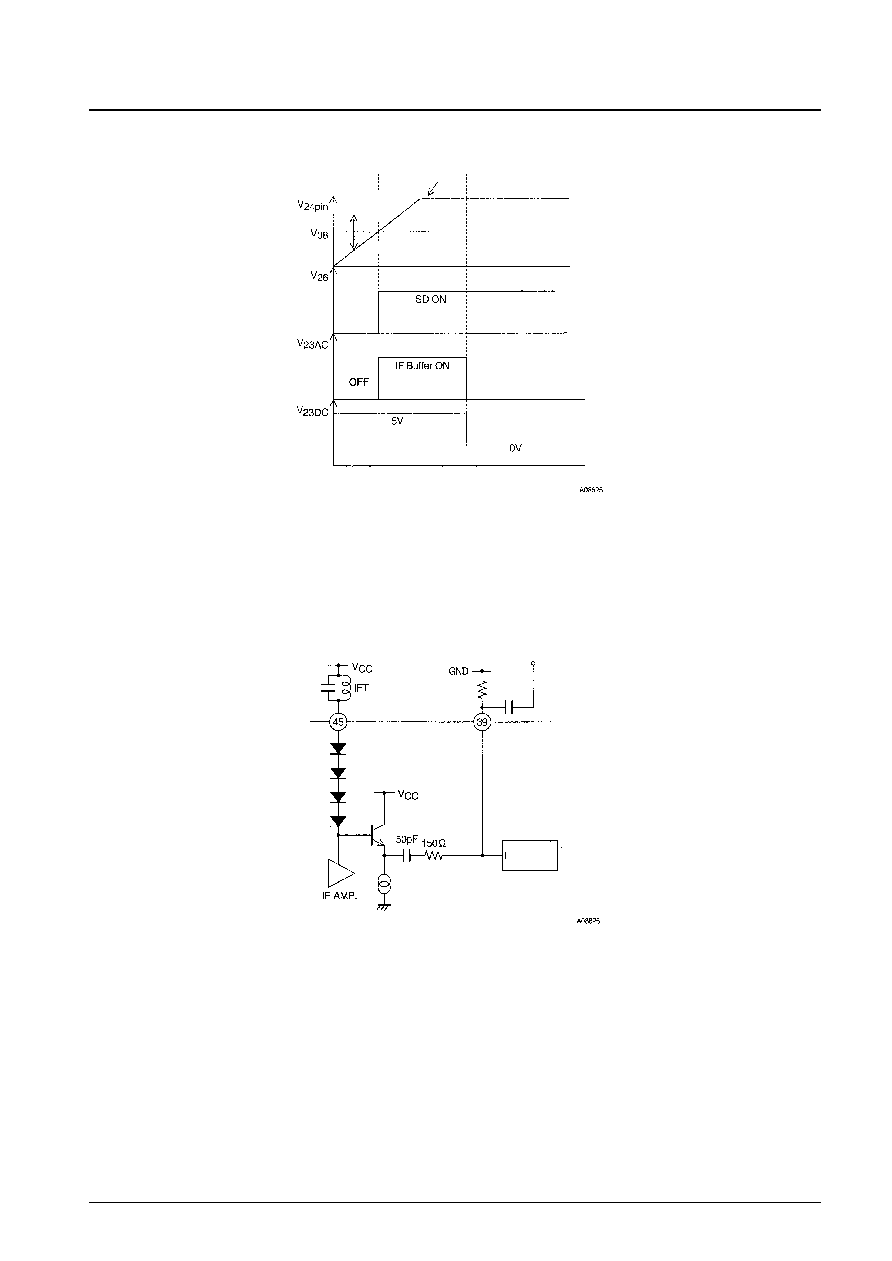
∑ AM mode
Pin 55: AM SD Adjustment Pin
No. 5724-22/38
LA1780M
∑ Pins that support AM stereo
∑ To attenuate the pin 39 AC level:
Add a capacitor between pin 39 and ground.
For example, if a capacitor is added between pin 39 and ground, and pin 51 is attached, the AM IF output will be
reduced by about 6 dB.
S-meter
Larger
R
55
Smaller R
35
Keyed
AGC
To an AM
stereo decoder
400-mV rms
450-kHz output
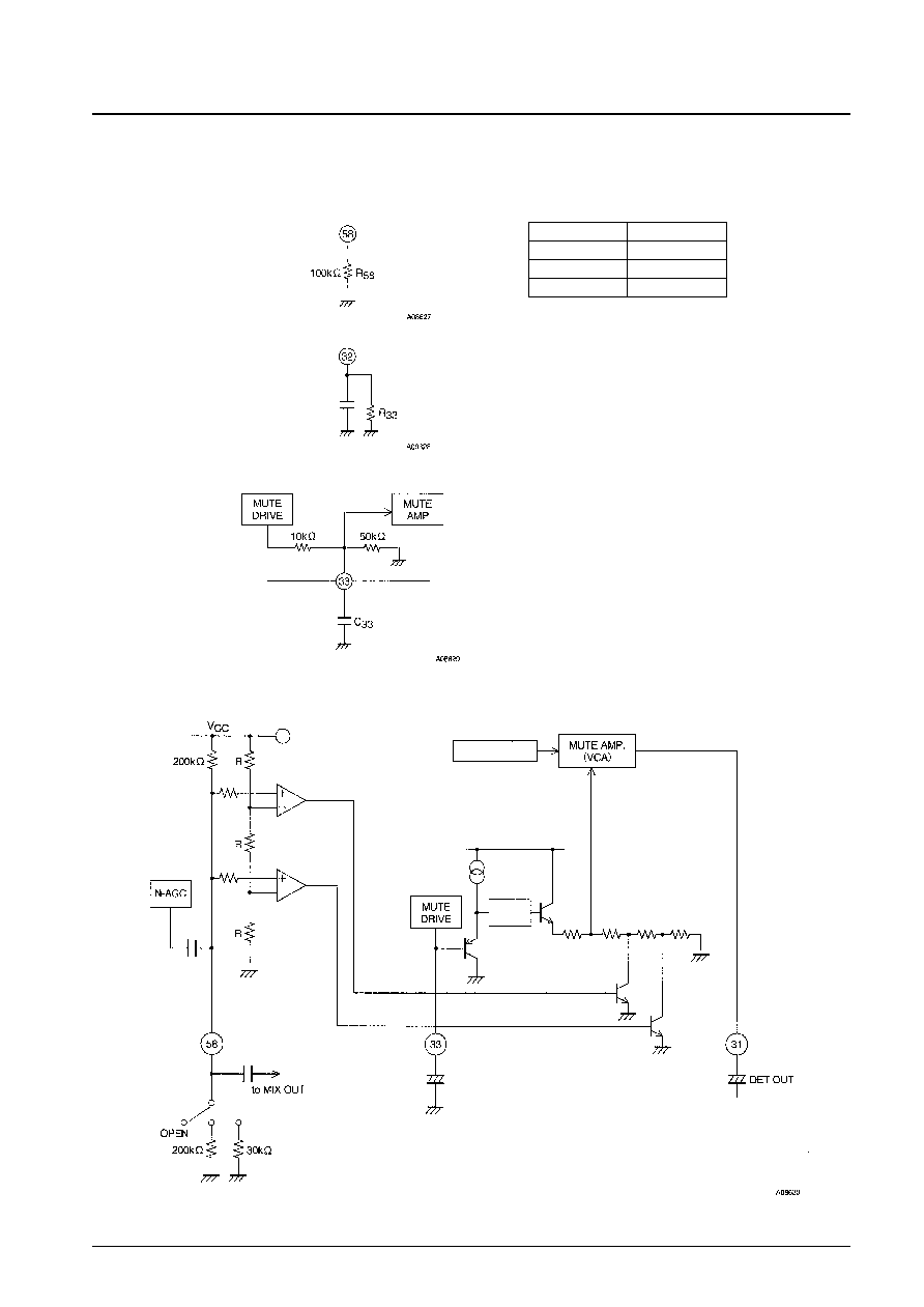
∑ Notes on the muting attenuation
The resistor between pin 58 and ground switches the muting attenuation to one of three levels, ≠20, ≠30, and ≠40 dB.
This is also related to the tuner's total gain.
No. 5724-23/38
LA1780M
R
Mute ATT
OPEN
≠20 dB
200k
≠30 dB
30k
≠40 dB
If R33 is reduced, the attenuation will be
reduced as listed in the table above.
Muting time constants
Attack: 10 k
◊
C33
Release: 50 k
◊
C33
Quadrature detector
Limiter
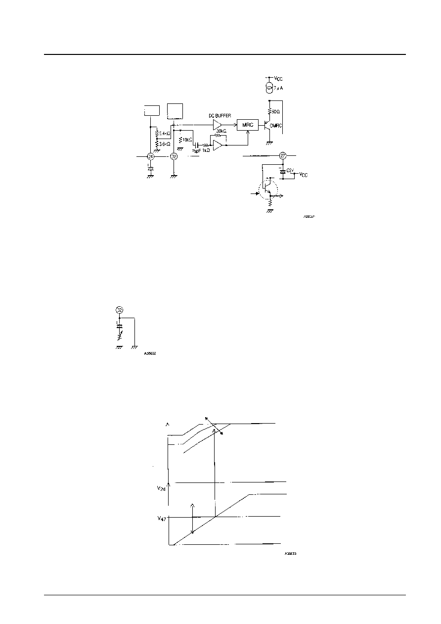
∑ MRC circuit
∑ If there is no AC noise on pin 32:
V27 will be about 2.5 V for an antenna input of 60 dBµ or higher.
∑ Since the MRC noise amplifier gain is fixed, the MRC circuit is adjusted by reducing the AC input level.
∑ The MRC circuit attack and release times are determined by the capacitor C27 on pin 27.
Attack: 7 µA
◊
C27
Release: 500
◊
C27
5. FM Soft Muting
By comparing the pin 47 mute on adjustment voltage to the S-meter voltage (V24), the muting on point can be adjusted.
No. 5724-24/38
LA1780M
S-meter
FM
S-meter
To SNC
Pin 28
Noise amplifier
fc = The MPF + AMP 70 kHz
Required external transistor: 2SC536 or equivalent
Reason: Since the LA1780M MRC is a simplified
circuit, an OMRC level shifter is required.
V24 = V27 ≠ V
BE
Q
MRC
Smaller R
47
Larger R
47
Larger
R
47
Smaller R
47
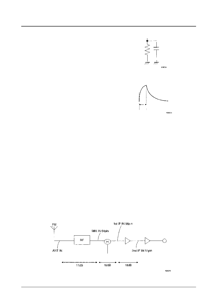
∑ Noise canceller notes
The characteristics of the noise canceller have been
improved by implementing the circuit that determines the
gate time in logic. In earlier noise canceller circuits, since
the time constant was determined with an RC circuit such
as the one shown in figure 5, the rise time was influenced
by the RC circuit time constant as show in figure 6. This
meant that the rise was delayed and the associated
switching delay resulted in a reduction of the circuit's
ability to exclude noise.
In the LA1780M, the rise time is made shorter by
implementing the circuit that determines the gate time in
logic. This allows the LA1780M to eliminate noise
reliably.
∑ Gain distribution (FM)
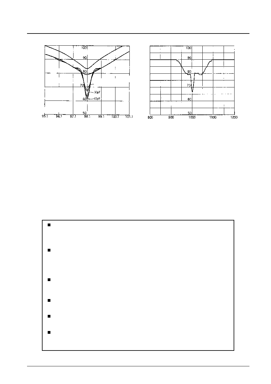
This section analyzes the gain in each of the blocks in the LA1780M when the Sanyo recommended circuit is used.
Test conditions
Ambient temperature:
26∞C
Antenna and mixer input frequency: 98.1 MHz
First and second IF input frequency: 10.7 MHz
Input levels when VSM = 2 V were measured to be:
Antenna input: 19 dBµ
Mixer input:
30 dBµ
First IF input:
42 dBµ
Second IF input: 60 dBµ
These values allow the gains in each block to be calculated as follows.
RF gain:
11 dB
Mixer gain: 12 dB
No. 5724-25/38
LA1780M
Figure 5
Figure 6

AM
This section analyzes the gain in each of the blocks in the LA1780 when the Sanyo recommended circuit is used.
Test conditions
Ambient temperature:
26∞C
Antenna and mixer 1 input frequency: 1 MHz
Mixer 2 input frequency:
10.71 MHz
IF and detector input frequencies:
450 kHz
An AM dummy is attached.
When an input level such that the output becomes ≠35 dBm is determined, the I/O characteristics of each stage were
determined to be as follows:
Antenna input: 9.5 dBµ
Mixer 1 input: 25.6 dBµ
Mixer 2 input: 29.5 dBµ
IF input:
36.0 dBµ
Detector input: 102.0 dBµ
These values allow the gains in each block to be calculated as follows.
RF gain:
16.1 dB
Mixer 1 gain: 3.9 dB
Mixer 2 gain: 6.5 dB
IF gain:
66.0 dB
No. 5724-26/38
LA1780M
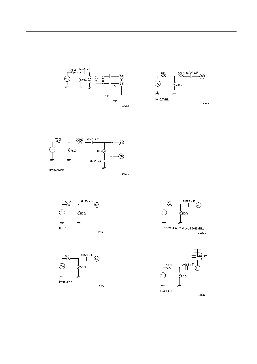
∑ Input circuits used at each stage
[FM]
Mixer input
First IF input
No. 5724-27/38
LA1780M
Actual
measurement
IF input
[AM]
First mixer input
Second mixer input
IF input
Detector input

∑ 3D AGC (keyed AGC) settings
∑ The antenna damping function operates by providing the pin diode antenna damping current from the pin when the
pin 2 voltage becomes equal to V
CC
≠ V
BE
.
∑ The noise AGC circuit operates as follows:
When the pin 39 voltage is greater than (6.4/3.6) times the pin 24 voltage, the ACG circuit is off.
When the pin 39 voltage is less than (6.4/3.6) times the pin 24 voltage, the ACG circuit is on.
No. 5724-28/38
LA1780M
S-meter
VS-meter
AM AGC System
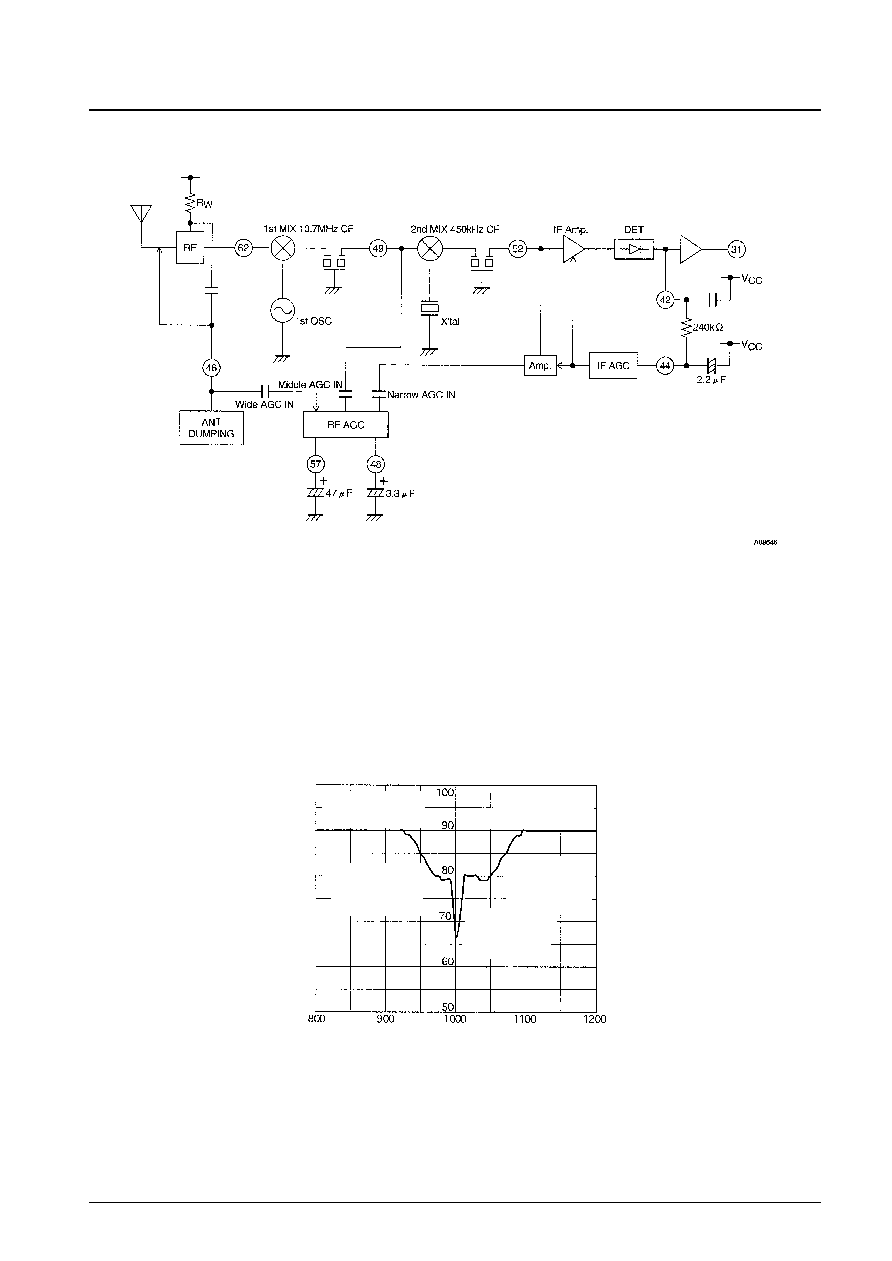
The LA1780M RF AGC is picked up from three locations.
∑ The wide AGC determined by Rw
∑ The middle AGC picked up from the pin 49 second mixer input
The operating bandwidth is 150 kHz to 180 kHz (the bandwidth of the 10.7 MHz CF)
∑ The narrow AGC picked up from pin 52
The operating bandwidth is 7 kHz (the bandwidth of the 450 kHz CF)
No. 5724-29/38
LA1780M
AM AGC Frequency Characteristics
AGC on level
Frequency, -- Hz
Wide AGC
Operates for wide-band
interfering stations.
Wide AGC
Operates for wide-band
interfering stations.
Middle AGC
Operates for interfering
stations that are
±70 kHz from the
received frequency.
Middle AGC
Operates for interfering
stations that are ±70
kHz from the received
frequency.
Narrow AGC
Operates at the
received frequency.

∑ Sample AM application using the LC72144 and the LA1780M
No. 5724-30/38
LA1780M
AM 1st IF
Step
FM IF
1
f
OSC
10.25 MHz
10.7 MHz
10 K, 1 K
10.7 MHz
2
f
OSC
10.35 MHz
10.8 MHz
9 K, 10 K
10.8 MHz

No. 5724-31/38
LA1780M
Crystal Oscillator Element (Kinseki, Ltd.)
HC-49/U-S
Frequency: 10.26 MHz
Load capacitance: 20 pF
Equivalent series resistance: 90
Coil Specifications (SUMIDA ELECTRIC CO., LTD.)
Application:
AM Block
∑ SA-359 (AM FILTER)
∑ SA-1063 (AM IF2)
∑ SA-1048 (AM ANT IN)
∑ SA-264 (AM IF1)
∑ SA-1062 (AM loading)
x ≠ y 16T
y ≠ z 16T
0.08 UEW
x ≠ y 75T
y ≠ z 75T
0.05 UEW
x ≠ z 74T
0.07 UEW
x ≠ y 30T
} ≠ { 19T
y ≠ z 151T
0.05 UEW
x ≠ z 850T
0.05 UEW
Prototype number
Model number
[AM Block]
AM FILTER
SA-1051
Y-5G (For the first mixer input: 5 mm diagonal)
AM OSC
SA-359
S-7LB
AM IF1 (MIX)
SA-264
PG78
SA-1111
PG57 (5 mm, high reliability)
SA-1009
P-5DJ (5 mm diagonal)
AM IF2
SA-1063
PG78
SA-1112
PG57 (5 mm, high reliability)
SA-265
P-5DJ (5 mm diagonal)
AM loading
SA-1062
MG78
AM antenna input
SA-1048
MG78
AM RF amplifier
RC875-222J
RC875
[FM Block]
FM RF
SA-1060
S-7LDJ
FM ANT
SA-1061
S-7LDJ
FM OSC
SA-1052
S-7LDJ
FM MIX
SA-266
P-7LFJ (Double balanced mixer)
FM DET
SA-208
QU-7L (Quadrature detector)
SA-360
QU57 (5 mm diagonal, quadrature detector)

No. 5724-32/38
LA1780M
FM Block
∑ SA-1060 (FM RF)
∑ SA-1052 (FM OSC)
∑ SA-208 (FM DET)
∑ SA-1061 (FM ANT)
∑ SA-266 (FM MIX)
} ≠ { 1T
0.10 UEW
z ≠ x 3T
z ≠ x 3T
0.16 UEW
} ≠ x 2T
} ≠ x 2T
0.18 UEW
{ ≠ z 18
1
T
4
0.08 UEW
z ≠ x 70
1
T
4
0.06 UEW
} ≠ { 3T
} ≠ { 3T
0.16 UEW
z ≠ x 3T
} ≠ y 6
1
T
2
y ≠ { 6
1
T
2
0.10 UEW
Coil Specifications (Toko INC)
[AM Block]
Toko Part No.
AM ANT
269ANS-0720
ANT
385BNS-027Z
Choke
187LY-222K
MIX LPF
A286LBIS-15327
AM 2nd MIX
L7TCS-3039A
AM OSC
V666SNS-213BY
AM IFT2
7PSG-5002
[FM Block]
AM, FM, MIX
3710H-1108FYH
FM DET
DM600DEAS-8407
FM ANT
666SNS-219NK
FM RF
666SNS-218AQ
FM OSC
V666SNS-205APZ

No. 5724-33/38
LA1780M
FM Block
∑ 3710H-1108FYH (AM ∑ FM ∑ MIX)
∑ 666SNS-219NK (FM ANT)
∑ V666SNS 205APZ (FM OSC)
∑ DM600DEAS-8407GLF (FM DET)
∑ 666SNS-218AQ (FM RF)
{ ≠ } 2
1
T
2
0.1¯ ZUEW
z ≠ x 2
1
T
2
} ≠ { 1T
0.1¯ ZUEW
z ≠ x 13T
z ≠ | 6
1
T
2
| ≠ x 6
1
T
2
} ≠ { 2T
0.07¯ ZUEW
} ≠ z 19
1
T
2
} ≠ { 2
1
T
2
z ≠ x 59T
0.07¯ ZUEW
} ≠ x 2
0.12¯ ZUEW
AM Block
∑ 269ANS-072Z (AM ANT)
∑ 187LY-222K (Choke)
∑ 385BNS-027Z (ANT)
∑ A286LBIS-15327 (MIX LPF)
x ≠ z 60T
0.06 3UEW
243
0.1¯ ZUEW
x ≠ z 60T
0.06¯ 3UEW
No. 5724-34/38
LA1780M
∑ L7TCS-3039A (AM 2nd MIX)
∑ 7PSG-500Z (AM IFTZ)
∑ V666SNS-213BY (AM OSC)
x ≠ z 152T
x ≠ y 25T
y ≠ z 127T
} ≠ { 16T
0.05¯ 3UEW
x ≠ z 148T
x ≠ y 74T
y ≠ z 74T
0.05¯ 3UEW
z ≠ x 24
1
T
2
z ≠ y 12
1
T
4
y ≠ x 12
1
T
4
0.1¯ ZUEW

No. 5724-35/38
LA1780M
FM I/O Characteristics
FM I/O Characteristics
Antenna input, -- dBµ
FM Distortion
Antenna input, -- dBµ
FM Sensitivity Suppression
Antenna input, -- dBµ
FM Gain Distribution (1)
Antenna input, -- dBµ
FM Gain Distribution (2)
Input, -- dBµ
Mixer I/O Characteristics
Input, -- dBµ
First IF I/O Characteristics
Mixer input, -- dBµ
First IF input, -- dBµ
Output, noise, AM output, LR output -- dB
HCC, SNC, RF AGC, muting voltage, S-
meter voltage, V
SM
-- V
Total harmonic distortion, THD -- %
Output, noise -- dB
Output, noise, AM output -- dB
DCV -- V
Mixer output -- dBµ
First IF output -- dBµ
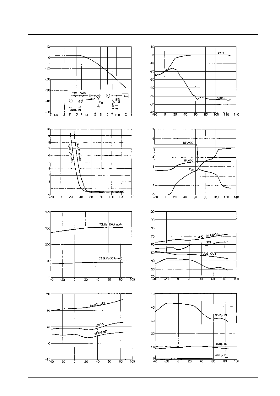
No. 5724-36/38
LA1780M
First IF Frequency Characteristics.
AM I/O Characteristics
Frequency, -- MHz
AM Distortion
Antenna input, -- dBµ
AM DC Characteristics
Antenna input, -- dBµ
FM Antenna Input Temperature Characteristics (1)
Antenna input, -- dBµ
FM Antenna Input Temperature Characteristics (2)
Ambient temperature, Ta -- ∞C
FM Antenna Input Temperature Characteristics (3)
Ambient temperature, Ta -- ∞C
FM Antenna Input Temperature Characteristics (4)
Ambient temperature, Ta -- ∞C
Ambient temperature, Ta -- ∞C
First IF output -- dB
Output, noise -- dB
Output -- dB
Total harmonic distortion, THD -- %
AGC, S-meter voltage -- V
Output - mV rms
S/N, AM output -- dB
AGC on, separation, input level -- dBµ
Antenna input -- dBµ
Separation, Sep -- dB
Separation

No. 5724-37/38
LA1780M
FM Antenna Input Temperature Characteristics (5)
FM Antenna Input Temperature Characteristics (6)
Ambient temperature, Ta -- ∞C
AM Antenna Input Temperature Characteristics (1)
Ambient temperature, Ta -- ∞C
AM Antenna Input Temperature Characteristics (2)
Ambient temperature, Ta -- ∞C
AM Antenna Input Temperature Characteristics (3)
Ambient temperature, Ta -- ∞C
FM Soft Muting (1)
Ambient temperature, Ta -- ∞C
FM Soft Muting (2)
Antenna input, -- dBµ
FM Soft Muting (3)
Antenna input, -- dBµ
Antenna input, -- dBµ
Total harmonic distortion, THD -- %
S-meter voltage, V
SM
-- V
AGC on level -- dBµ
AGC FOM, S/N, QS, SD sensitivity -- dBµ
Total harmonic distortion, THD -- %
S-meter voltage, V
SM
-- V
Output -- mV rms
Output, noise -- dB
Output, noise -- dB
Output -- dB
Output -- dB
Specifications of any and all SANYO products described or contained herein stipulate the performance,
characteristics, and functions of the described products in the independent state, and are not guarantees
of the performance, characteristics, and functions of the described products as mounted in the customer's
products or equipment. To verify symptoms and states that cannot be evaluated in an independent device,
the customer should always evaluate and test devices mounted in the customer's products or equipment.
SANYO Electric Co., Ltd. strives to supply high-quality high-reliability products. However, any and all
semiconductor products fail with some probability. It is possible that these probabilistic failures could
give rise to accidents or events that could endanger human lives, that could give rise to smoke or fire,
or that could cause damage to other property. When designing equipment, adopt safety measures so
that these kinds of accidents or events cannot occur. Such measures include but are not limited to protective
circuits and error prevention circuits for safe design, redundant design, and structural design.
In the event that any or all SANYO products (including technical data, services) described or contained
herein are controlled under any of applicable local export control laws and regulations, such products must
not be exported without obtaining the export license from the authorities concerned in accordance with the
above law.
No part of this publication may be reproduced or transmitted in any form or by any means, electronic or
mechanical, including photocopying and recording, or any information storage or retrieval system,
or otherwise, without the prior written permission of SANYO Electric Co., Ltd.
Any and all information described or contained herein are subject to change without notice due to
product/technology improvement, etc. When designing equipment, refer to the "Delivery Specification"
for the SANYO product that you intend to use.
Information (including circuit diagrams and circuit parameters) herein is for example only; it is not
guaranteed for volume production. SANYO believes information herein is accurate and reliable, but
no guarantees are made or implied regarding its use or any infringements of intellectual property rights
or other rights of third parties.
PS No. 5724-38/38
LA1780M
This catalog provides information as of March, 2000. Specifications and information herein are subject to
change without notice.
AGC on level -- dBµ
With a 10-pF capacitor
connected to pin 58
AGC on level -- dBµ
Frequency, -- MHz
Frequency, -- Hz
AM AGC Frequency Characteristics
AM AGC Frequency Characteristics