 | –≠–ª–µ–∫—Ç—Ä–æ–Ω–Ω—ã–π –∫–æ–º–ø–æ–Ω–µ–Ω—Ç: LA1833NM | –°–∫–∞—á–∞—Ç—å:  PDF PDF  ZIP ZIP |
Ordering number : ENN6568
D1500RM (OT) No. 6568-1/10
Overview
The LA1833N/NM is an AM/FM IF and MPX system-on-
chip IC that supports electronic tuning for home stereo
systems. It is optimal for use in auto-seek systems that use
SD (station detect) and IF counting in parallel.
Functions
∑ AM: RF amplifier, mixer, oscillator, IF amplifier,
detector, AGC, SD, oscillator buffer, IF buffer, and
stereo IF output
∑ FM IF: IF amplifier, quadrature detector, S meter, SD,
S-curve detector, IF buffer
∑ MPX: PLL stereo decoder, stereo indicator, forced
mono, VCO stop, audio muting, adjacent channel
interference reduction function, pilot canceller
Features
∑ Improvements over the LA1832
-- The MPX VCO circuit has been integrated on the
same IC (no ceramic element required)
-- Built-in adjacent channel interference reduction
function (114 kHz, 190 kHz)
-- Built-in pilot canceler function (19 kHz)
-- AM and FM output levels can be set independently
-- Improved FM reception characteristics (IF beating
improved)
∑ Other features
-- Pin arrangement nearly identical to that of the
LA1832
-- AM coil specifications can be the same as those used
for the LA1832.
-- ST operating dynamic range improved over that of
the LA1833
-- FM total harmonic distortion detuning
characteristics and signal-to-noise ratio improved
over those of the LA1833
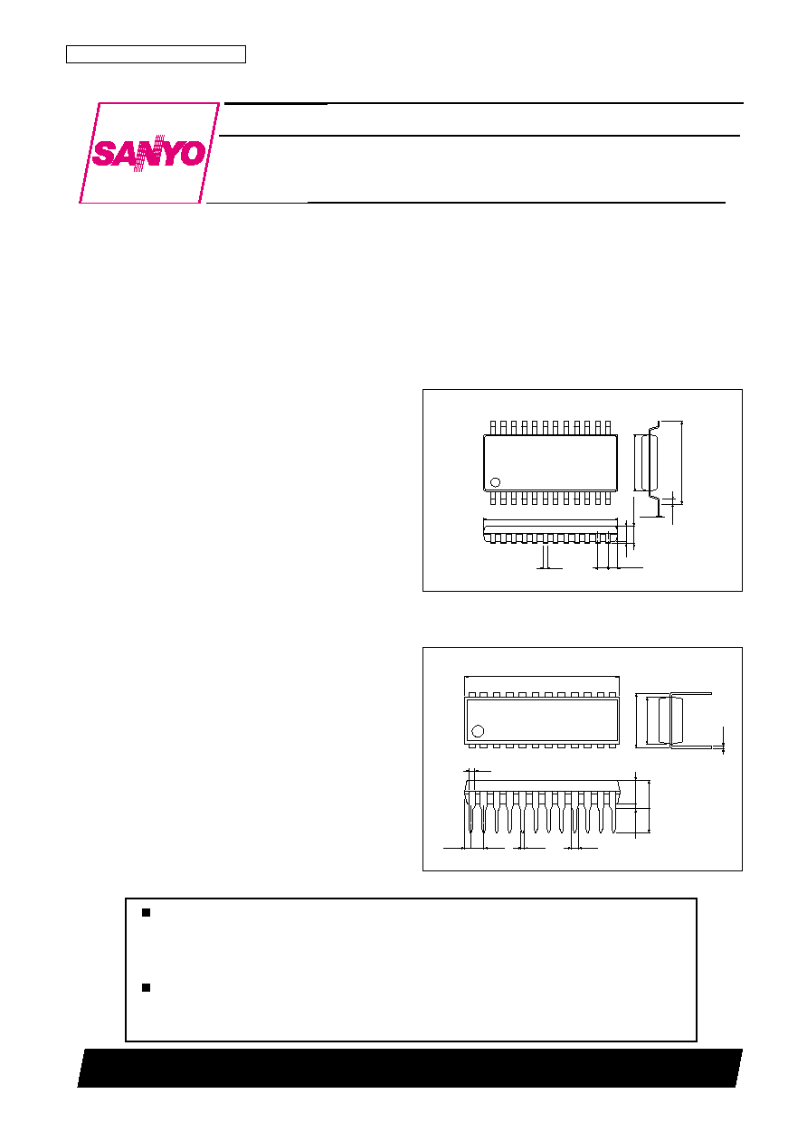
Package Dimensions
unit: mm
3112A-MFP24S
unit: mm
3067A-DIP24S
1
12
24
13
12.5
(0.75)
1.0
0.15
0.35
5.4
7.6
0.63
1.7max
1.5
0.1
SANYO: MFP24S (300 mil)
[LA1833N]
LA1833N, 1833NM
SANYO Electric Co.,Ltd. Semiconductor Company
TOKYO OFFICE Tokyo Bldg., 1-10, 1 Chome, Ueno, Taito-ku, TOKYO, 110-8534 JAPAN
System-on-Chip Tuner IC for Home Stereo Systems
Monolithic Linear IC
Any and all SANYO products described or contained herein do not have specifications that can handle
applications that require extremely high levels of reliability, such as life-support systems, aircraft's
control systems, or other applications whose failure can be reasonably expected to result in serious
physical and/or material damage. Consult with your SANYO representative nearest you before using
any SANYO products described or contained herein in such applications.
SANYO assumes no responsibility for equipment failures that result from using products at values that
exceed, even momentarily, rated values (such as maximum ratings, operating condition ranges, or other
parameters) listed in products specifications of any and all SANYO products described or contained
herein.
0.48
(3.25)
3.3
3.9max
0.51min
21.0
(0.71)
1.78
0.25
7.62
6.4
1
12
24
13
0.95
0.9
SANYO: DIP24S (300 mil)
[LA1833NM]

No. 6568-2/10
LA1833N, 1833NM
Parameter
Symbol
Conditions
Ratings
Unit
Maximum supply voltage
V
CC
max
9
V
(LA1833N)
400
mW
Allowable power dissipation
Pd max
(LA1833NM) (Ta
45∞C)
400
mW
(LA1833NM) (Ta = 70∞C)
270
mW
Operating temperature
Topr
≠20 to +70
∞C
Storage temperature
Tstg
≠40 to +125
∞C
Specifications
Maximum Ratings
at Ta = 25∞C
Parameter
Symbol
Conditions
Ratings
Unit
Recommended supply voltage
V
CC
5
V
Operating supply voltage range
V
CC
op
4 to 8
V
Operating Conditions
at Ta = 25∞C
Parameter
Symbol
Conditions
Ratings
Unit
min
typ
max
[FM Mono Characteristics: fc = 10.7 MHz, fm = 1 kHz]
Current drain
I
CCO
-FM
No input
18
28
38
mA
Demodulator output
V
O
-FM
100 dBµ, 100% mod. The pin 13 output
210
330
420
mVrms
Channel balance
C.B-mono
100 dBµ, 100% mod.
≠1.5
0
1.5
dB
The ratio (pin 13 output)/(pin 14 output)
Total harmonic distortion (mono)
THD-FM
100 dBµ, 100% mod. The pin 13 output
0.5
1.5
%
Signal-to-noise ratio
S/N-FM
100 dBµ, 100% mod. The pin 13 output
70
78
dB
AM rejection ratio
AMR
100 dBµ, AM = 30% mod. fm = 1 kHz
45
63
dB
Input limiting voltage
≠3dBL. S
100 dBµ, 100% mod. The pin 13 output
34
42
dBµ
Referenced to the output, when the input is down by ≠3 dB
SD LED on sensitivity
SD-On-FM
32
42
52
dBµ
IF counter buffer output
V
IFBuff
-FM 100 dBµ, the pin 10 output
200
275
400
mVrms
Muting attenuation
Mute Att
100 dBµ, 100% mod. fm = 1 kHz
76
dB
[Stereo Characteristics: fc = 10.7 MHz, 100 dBµ, fm = 1 kHz, L + R = 90%, pilot = 10%]
Separation
Sep
Left channel modulated,
28
42
dB
the ratio (pin 13 output)/(pin 14 output)
Stereo on level
ST-on
The pilot modulation level such that V7 becomes
1.5
3.5
5.5
%
less than 0.7 V
Total harmonic distortion (main)
THD-main L + R modulation, the pin 13 output
0.7
1.5
%
Adjacent channel interference
Brej-3rd
fs = 113 kHz, Vs = 90%, Pilot = 10%; the pin 13 output
36
dB
rejection ratio
with respect to an L ≠ R modulated 1 kHz demodulator output
Adjacent channel interference
Brej-5th
fs = 189 kHz, Vs = 90%, Pilot = 10%; the pin 13 output
41
dB
rejection ratio
with respect to an L ≠ R modulated 1 kHz demodulator output
Carrier leakage
CL
L + R = 90%, De-emph asis 50 µs, Pilot = 10%
38
44
dB
[AM Characteristics: fc = 1000 kHz, fm = 1 kHz]
Current drain
I
CCO
-AM
No input
11
22
33
mA
Detector output
V
O
-AM (1) 23 dBµ, 30% modulation. The pin 13 output
40
80
160
mVrms
Detector output
V
O
-AM (2) 80 dBµ, 30% modulation. The pin 13 output
90
160
230
mVrms
Signal-to-noise ratio
S/N-AM (1) 23 dBµ, 30% modulation. The pin 13 output
16
21
dB
S/N-AM (2) 80 dBµ, 30% modulation. The pin 13 output
48
54
dB
Total harmonic distortion
THD-AM (1) 80 dBµ, 30% modulation. The pin 13 output
0.4
1.1
%
THD-AM (2) 100 dBµ, 30% modulation. The pin 13 output
0.5
1.3
%
SD LED on sensitivity
SD-On-AM
14
24
34
dBµ
Local oscillator buffer output
V
OSC
-AM No input, the pin 24 output
140
200
mVrms
IF counter buffer output
V
IFBuff
-AM 80 dBµ, no modulation, the pin 10 output
140
285
400
mVrms
Electrical Characteristics
at V
CC
= 5 V, in the specified test circuit

No. 6568-3/10
LA1833N, 1833NM
Pin Descriptions
Pin No.
Pin
Voltage (V)
Functional description
Equivalent circuit
1
FM IF input
Vreg
ILA00220
1
3
Continued on next page.
The input impedance, r
i
, is 330
2
ILA00221
2
AM MIX output
V
CC
The mixer coil is connected between pins
2 and 9
ILA00222
3
3
REG
2.1
Vreg = 2.1 V
ILA00223
4
4
AM IF input
Vreg
The input impedance, ri, is 2 k
5
GND
0
ILA00224
7
6
6
7
Tu-LED
ST-LED
Also functions as the
AM stereo IF output
V
CC
These are active-low open-collector
outputs.
Set up the current flowing in to these pins
to exceed 100 µA.
ILA00225
8
8
FM-DET
V
CC
≠ 2.1
Recommended ceramic discriminators
FCD1070MA11UK2L (TDK)
CDA10.7MG86N (Murata Mfg. Co., Ltd.)
9
V
CC
5.0
ILA00226
10
10
AM/FM IF counter
output
Also functions as a
control switch
Also functions as the
muting switch
0
V10
0.5 V: Reception state (normal)
1.4 V
V10
2.2 V: Muting on state.
V10
3.5 V: Muting on and IF counter on
(seek state).

No. 6568-4/10
LA1833N, 1833NM
Continued from preceding page.
Pin No.
Pin
Voltage (V)
Functional description
Equivalent circuit
11
Phase comparator
filter connection
Also functions as the
FM/AM switching
input
V
CC
≠ 1.0
ILA00227
11
Continued on next page.
The IC switches to AM mode if a current in
excess of 200 µA flows from this pin
12
ILA00228
12
Pilot detector filter
connection
Also functions as the
forced mono setting
Also functions as the
VCO stop control
V
CC
≠ 1.0
The IC switches to forced mono mode if a
current in excess of 50 µA flows from this
pin.
The VCO circuit is stopped if a current in
excess of 200 µA flows from this pin.
(
)
ILA00229
13
14
13
14
Left output
Right output
1.8
The output impedance, r
o
, is 3.3 k
ILA00230
15
3
15
Pilot canceller output
Vreg
ILA00231
16
RNF
16
Decoder input
Vreg
Inverting input
RNF = 20 k
ILA00232
17
17
PLL input
Vreg
The input impedance, r
i
, is 20 k
ILA00234
19
100V
19
AM detector output
0 (FM)
1.5 (AM)
The output impedance, r
o
, is 10 k
ILA00233
18
18
FM demodulator output
Vreg
The output impedance, r
o
, is 2.3 k
.
The separation can be adjusted by
changing the value of the capacitor
connected between this pin and ground.

No. 6568-5/10
LA1833N, 1833NM
Continued from preceding page.
Pin No.
Pin
Voltage (V)
Functional description
Equivalent circuit
20
S meter
Also functions as the
AM AGC
0.2 (FM)
0.9 (AM)
ILA00235
20
R
Internal load resistor R = 13.9 k
.
The SD response speed during seek
operations is set by the value of the
external capacitor connected to pin 20.
21
ILA00236
21
AM RF-IN
Vreg
Pin 21 and pin 22 (the AFC voltage) are
used at the same potential
ILA00237
22
22
AFC
Vreg
The FM SD bandwidth can be adjusted by
an external resistor connected between
pin 22 and pin 3 (the regulator voltage).
Note: A bandwidth of 180 kHz or higher is
appropriate for the FM SD bandwidth.
ILA00238
23
23
OSC
V
CC
The oscillator coil is connected between
pin 23 and pin 9 (the V
CC
voltage).
Note: The oscillator coil impedance
(secondary side) must be at least
5 k
.
ILA00239
24
R
24
Oscillator buffer
Also functions as the
FM SD adjustment
V
CC
≠ 1.4
The FM SD sensitivity can be adjusted
with an external resistor on pin 24.
R = 200
Note: The resistance of the pin 24 external
resistor must be at least 3.3 k
.

No. 6568-6/10
LA1833N, 1833NM
Block Diagram
ILA00240
24
23
22
21
20
19
FM-IN
(10.7MHz)
450kHz
+
+
+
+
R
L
B
UFF
ALC
AG
C
AM
IF
AM
DET
AM
MIX
FM
BAND-W
AM
RF
.
AMP
OSC
B
UFF
VT
FM SD
ADJ
OSC
RF
V
-SM
AM
OSC
S-CUR
VE
FM
DET
FM
IF
LEVEL
DET
TUNING
DRIVE
COMP
AM / FM
IF
B
UFF
GND
REG
STEREO
SW
FF
38k
VCO
304kHz
P-DET
ÿ
PILO
T
DET
FF
19k
0
FF
19k
2
PILO
T
CANCEL
DECODER
ANTI-BIRDIE
V
CC
2
3
4
5
6
7
8
10
11
+
+
+
12
TU-LED
ST-LED
AM / FM
IF-BUFF
AM
MONO
FM
ST
V
CC
(4.0 to 8.0 V)
SEEK
MUTE
18
17
16
15
14
13
9
1
AM stereo IF output

No. 6568-7/10
LA1833N, 1833NM
Test Circuit
ILA00241
L OUT
R OUT
0.015
µ
F
0.015
µ
F
0.0047
µ
F
0.1
µ
F
0.01
µ
F
39m
39pF
20pF
4.7
µ
F
0.047
µ
F
0.047
µ
F
10
µ
F
1000pF
65k
20k
20k
0 dB
24
23
22
21
20
19
FM-IN
(10.7MHz)
HW6215
0.047
µ
F
0.047
µ
F
33
µ
F
300
75
+
2
3
5
6
7
8
10
*
*
*
*
*
*
*
*
*
*
**
*
*
11
12
MFP = 33
TU-LED
LA1833N / 1833NM
ST-LED
AM IF
AM / FM
IF-BUFF
AM
0.47
µ
F
1
µ
F
1
µ
F
3k
MONO
FM
V
CC
Top view
5.0 V
18
17
16
15
14
13
9
1
4
SEEK
NORMAL
20pF
1000pF
1000pF
V-ST
V-SD
100
50k
50k
+
+
+
OSC
B
UFF
6.8k
1000pF
HW50425
AM-IN
(1MHz)
+
+
+
22
µ
F
3.3
µ
F
50
5.6k
A
A
LPF
LPF
CDA10.7MG1-B
(For the DUT socket
printed circuit board)
The places that differ with the LA1833 are (1) the value of the pin 8 resistor and (2) the circuits in the vicinity of pins 17
and 18.
*
: Pins with the same functionality as those on the LA1832.

No. 6568-8/10
LA1833N, 1833NM
0
--10
--20
--40
--30
--60
--50
--70
--80
--90
20
0
--20
--40
--60
--80
--100
10
8
6
4
2
0
12
0
50
100
150
ILA00242
ILA00244
4
2
6
10
8
60
55
50
40
45
35
30
25
20
ILA00245
2
10
4
6
8
20
0
--20
--40
--60
--80
10
8
6
4
2
0
ILA00246
20
0
40
140
80
100
120
60
S
AM
N
3.0
2.5
1.5
2.0
1.0
0.5
0
10.55
10.65
10.75
10.85
10.6
10.7
10.8
ILA00243
THD
N
AM
S
Qs
3dB LS
V
O
Noise
AGC
SD - OUT
THD(80%Mod)
THD(30%Mod)
0
--20
--40
--60
--10
--30
--50
--80
--70
1.2
1.0
0.8
0.6
0.4
0.2
0
1.6
1.4
ILA00247
4
2
6
10
8
Noise
Vout
THD(80%Mod)
THD(30%Mod)
80
60
40
20
70
50
30
0
10
ILA00248
4
2
6
10
8
AGC
SD -- ON
SD - OUT
100
80
60
40
20
0
ILA00249
--40
100
--20
0
20
40
60
80
S / N
SD -- ON
--3dB LS
Input -- dBµ
Output, -- dBV
Total harmonic distortion, THD -- %
Frequency -- MHz
Demodulator output, V
O
-- dBm
Supply voltage, V
CC
-- V
Supply voltage, V
CC
-- V
SD on range, Qs -- dBµ
3 dB limiting sensitivity, Qs -- dBµ
Supply voltage, V
CC
-- V
Input -- dBµ
Output, -- dBµ
Output, -- dBV
Useable sensitivity, Qs -- dBµ
SD sensitivity, SD -- dBµ
Supply voltage, V
CC
-- V
Ambient temperature, Ta -- ∞C
3 dB limiting sensitivity, 3dBLS -- dB
Signal-to-noise ratio, SD on, 3dBLS -- dB
FM IF I/O Characteristics
FM IF THD Detuning Characteristics
FM IF V
CC
Characteristics
FM IF V
CC
Characteristics
AM Characteristics
AM V
CC
Characteristics
AM V
CC
Characteristics
FM IF Temperature Characteristics
SD on range
Useable sensitivity
Total harmonic distortion, THD -- %
SD, AGC -- V
Total harmonic distortion, THD -- %

No. 6568-9/10
LA1833N, 1833NM
3.0
2.5
2.0
1.5
1.0
0.5
0
ILA00250
--40
100
--20
0
20
40
60
80
60
50
40
30
20
10
0
ILA00252
--40
100
--20
0
20
40
60
80
10
1.0
0.1
THD -- fm
ILA00254
100000
10
100
1000
10000
10
1.0
0.1
2
3
5
7
2
3
5
7
THD -- V
CC
ILA00256
0
1
2
3
4
5
6
7
8
9
50
40
30
20
10
0
Sep -- fm
ILA00255
100000
10
100
1000
10000
3.0
2.5
2.0
1.5
1.0
0.5
0
ILA00253
--40
100
--20
0
20
40
60
80
100dB
µ
50dB
µ
0dB
µ
70
60
50
40
30
20
10
0
3.0
2.5
2.0
1.5
1.0
0.5
0
3.5
ILA00251
0
--20
--40
20
100
40
60
80
100
80
60
40
20
0
Sep, S / N -- V
CC
ILA00257
2
10
4
6
8
THD
Sep
Pilot ON
SD -
- ON
23dB
µ
80dB
µ
20dB
µ
80dB
µ
0dB
µ
THD main
THD sub
THD st
Sep L
Sep R
THD sub
THD main
THD mono
THD st
Sep L
Sep R
S / N
Ambient temperature, Ta -- ∞C
S-meter voltage, V
SM
-- V
Channel separation, Sep -- dB
Ambient temperature, Ta -- ∞C
Signal-to-noise ratio, S/N -- dB
SD on level -- dBµ
Ambient temperature, Ta -- ∞C
Ambient temperature, Ta -- ∞C
AGC voltage, V
AGC
-- V
Modulation frequency, fm -- kHz
Modulation frequency, fm -- kHz
Channel separation, Sep -- dB
Total harmonic distortion, THD -- %
Supply voltage, V
CC
-- V
Supply voltage, V
CC
-- V
Channel separation, Sep -- dB
Signal-to-noise ratio, S/N -- dB
FM IF Temperature Characteristics
FM ST V
CC
Characteristics
AM Temperature Characteristics
AM Temperature Characteristics
Total harmonic distortion, THD, pilot on -- %
Total harmonic distortion, THD -- %

PS No. 6568-10/10
LA1833N, 1833NM
This catalog provides information as of December, 2000. Specifications and information herein are
subject to change without notice.
Specifications of any and all SANYO products described or contained herein stipulate the performance,
characteristics, and functions of the described products in the independent state, and are not guarantees
of the performance, characteristics, and functions of the described products as mounted in the customer's
products or equipment. To verify symptoms and states that cannot be evaluated in an independent device,
the customer should always evaluate and test devices mounted in the customer's products or equipment.
SANYO Electric Co., Ltd. strives to supply high-quality high-reliability products. However, any and all
semiconductor products fail with some probability. It is possible that these probabilistic failures could
give rise to accidents or events that could endanger human lives, that could give rise to smoke or fire,
or that could cause damage to other property. When designing equipment, adopt safety measures so
that these kinds of accidents or events cannot occur. Such measures include but are not limited to protective
circuits and error prevention circuits for safe design, redundant design, and structural design.
In the event that any or all SANYO products (including technical data, services) described or contained
herein are controlled under any of applicable local export control laws and regulations, such products must
not be exported without obtaining the export license from the authorities concerned in accordance with the
above law.
No part of this publication may be reproduced or transmitted in any form or by any means, electronic or
mechanical, including photocopying and recording, or any information storage or retrieval system,
or otherwise, without the prior written permission of SANYO Electric Co., Ltd.
Any and all information described or contained herein are subject to change without notice due to
product/technology improvement, etc. When designing equipment, refer to the "Delivery Specification"
for the SANYO product that you intend to use.
Information (including circuit diagrams and circuit parameters) herein is for example only; it is not
guaranteed for volume production. SANYO believes information herein is accurate and reliable, but
no guarantees are made or implied regarding its use or any infringements of intellectual property rights
or other rights of third parties.
8
6
4
0
2
--2
--4
--6
--8
10
15
20
25
30
35
3.0
2.5
2.0
1.5
1.0
0.5
0
V
L
on, off -- V
CC
ILA00258
ILA00259
2
10
4
6
8
V
L
off
V
L
on
CR+
CR--
Supply voltage, V
CC
-- V
Stereo sensitivity, V
L
-- %
Pilot input voltage -- mV
Capture range, CR -- %
Capture Range Characteristics