 | –≠–ª–µ–∫—Ç—Ä–æ–Ω–Ω—ã–π –∫–æ–º–ø–æ–Ω–µ–Ω—Ç: LA1845N | –°–∫–∞—á–∞—Ç—å:  PDF PDF  ZIP ZIP |

Ordering number : ENN7185
91002RM (OT) No. 5888-1/10
Overview
The LA1845N/1845NM is designed for use in mini
systems and is a single-chip tuner IC that provides
electronic tuning functions using SD/IF-count technigue.
It incorporates a pilot canceler and an adjustment-free
MUX VCO circuit, thus allows additional parts to be
reduced.
Functions
∑ AM:
RF amplifier, mixer, oscillator, IF amplifier,
detector, AGC, SD, oscillator buffer, IF buffer,
stereo IF output, AGC time constant switch
∑ FM IF: IF amplifier, quadrature detector, S-meter, SD
(signal detection), S-curve detection, IF buffer
output
∑ MPX:
PLL stereo decoder, stereo display, forced
monaural, VCO stop, audio muting, adjacent
channel interference rejection function, pilot
canceler
Features
∑ Integrated MPX VCO (ceramic resonators are no longer
required.)
∑ Built-in adjacent channel interference rejection function
(114 kHz, 190 kHz)
∑ Supports both SD and IF-count techniques
∑ Both FM SD sensitivity and bandwidth can be set
∑ Pilot canceler built in.
Package Dimensions
unit: mm
3067A-DIP24S
unit: mm
3112A-MFP24S
1
12
24
13
12.5
(0.75)
1.0
0.15
0.35
5.4
7.6
0.63
1.7max
1.5
0.1
SANYO: MFP24S
[LA1845NM]
0.48
(3.25)
3.3
3.9max
0.51min
21.0
(0.71)
1.78
0.25
7.62
6.4
1
12
24
13
0.95
0.9
SANYO: DIP24S
[LA1845N]
LA1845N, 1845NM
SANYO Electric Co.,Ltd. Semiconductor Company
TOKYO OFFICE Tokyo Bldg., 1-10, 1 Chome, Ueno, Taito-ku, TOKYO, 110-8534 JAPAN
Single-Chip Home Stereo IC
Monolithic linear IC
Any and all SANYO products described or contained herein do not have specifications that can handle
applications that require extremely high levels of reliability, such as life-support systems, aircraft's
control systems, or other applications whose failure can be reasonably expected to result in serious
physical and/or material damage. Consult with your SANYO representative nearest you before using
any SANYO products described or contained herein in such applications.
SANYO assumes no responsibility for equipment failures that result from using products at values that
exceed, even momentarily, rated values (such as maximum ratings, operating condition ranges, or other
parameters) listed in products specifications of any and all SANYO products described or contained
herein.
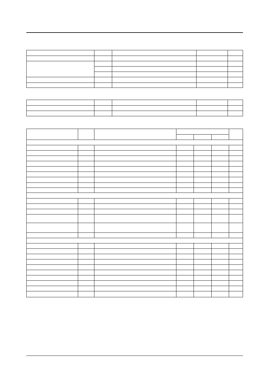
Specifications
Maximum Ratings
at Ta = 25∞C
Operating Conditions
at Ta = 25∞C
Operating Characteristics
at Ta = 25∞C, V
CC
= 8 V, in the specified test circuit.
No. 5888-2/10
LA1845N, 1845NM
Parameter
Symbol
Conditions
Ratings
Unit
Maximum supply voltage
V
CC
max
9
V
Pd max
Ta
45∞C
400
mW
Allowable power dissipation
Pd max
Ta = 80∞C (DIP)
400
mW
Pd max
Ta = 80∞C (MFP)
260
mw
Operating temperature
Topr
≠20 to +80
∞C
Storage temperature
Tstg
≠40 to +125
∞C
Parameter
Symbol
Conditions
Ratings
Unit
Recommended supply voltage
V
CC
8
V
Operating supply voltage range
V
CC
op
Ta = 80∞C
4.3 to 8.5
V
Parameter
Symbol
Conditions
Ratings
Unit
min
typ
max
[FM Mono Characteristics] fc = 10.7 MHz, Vi = 100 dBµ, fm = 1 kHz, Mod = 75 kHz
Current drain
I
CCO-FM
With no input signal
20
30
40
mA
Demodulator output
V
OFM
100 dBµ, 100% modulation, fm = 1 kHz
230
360
460
mVrms
Total harmonic distortion
THD
FM
100 dBµ, 100% modulation, fm = 1 kHz
0.35
1.5
%
Signal-to-noise ratio
S/N
FM
100 dBµ, 100% modulation, fm = 1 kHz
73
80
dB
AM rejection ratio
AMR
100 dBµ, AM 30% modulation, fm = 1 kHz
47
65
dB
3 dB sensitivity
100 dBµ, 100% modulation, fm = 1 kHz, -3 dB input
32
40
dBµ
SD sensitivity
0% modulation
38
47
56
dBµ
IF counter buffer output
V
IFBuff-FM
100 dBµ, the pin 13 output
80
120
160
mVrms
Mute attenuation
Mute-Att
100 dBµ, 100% modulation, fm = 1 kHz
75
85
dB
[FM Stereo Characteristics] fc = 10.7 MHz, Vi = 100 dBµ, fm = 1 kHz, L + R = 90%, Pilot = 10%
Separation
Sep
L
Left channel modulated. The pin 16 output/the pin 17 output
30
42
dB
Stereo on level
ST
ON
The pilot modulation such that V7 falls under 0.7 V
1.5
3.5
5.5
%
Total harmonic distortion
THD-main
Left + right modulation. The pin 16 output.
0.45
1.5
%
fs = 113 kHz, Vs = 90%, pilot = 10%
Adjacent channel rejection ratio 1
Brej-3rd
The left - right modulation, demodulated output
36
dB
fs = 189 kHz, Vs = 90%, pilot = 10%
Adjacent channel rejection ratio 2
Brej-5th
The left - right modulation, demodulated output
41
dB
Carrier leak
L + R = 90%, pilot = 10% reference, pilot = 10% output
38
44
dB
[AM Characteristics] fc = 1000 kHz, Vi = 80 dBµ, fm = 1 kHz, Mod = 30%
Current drain
I
CCO-AM
With no input signal
13
27
39
mA
Detector output 1
V
OAM1
23 dBµ, 30% modulation, fm = 1 kHz
40
80
160
mVrms
Detector output 2
V
OAM2
80 dBµ, 30% modulation, fm = 1 kHz
90
160
230
mVrms
Signal-to-noise ratio 1
S/N
AM1
23 dBµ, 30% modulation, fm = 1 kHz
17
23
dB
Signal-to-noise ratio 2
S/N
AM2
80 dBµ, 30% modulation, fm = 1 kHz
46
52
dB
Total harmonic distortion 1
THD
AM1
80 dBµ, 30% modulation, fm = 1 kHz
0.4
1.1
%
Total harmonic distortion 2
THD
AM2
107 dBµ, 30% modulation, fm = 1 kHz
0.5
1.3
%
SD sensitivity
0% modulation
11
20
29
dBµ
Local oscillator buffer output
V
OSC-AM
With no input signal
100
140
200
mVrms
IF counter buffer output
V
IFBuff-AM
23 dBµ
140
285
400
mVrms
Block Diagram
AC Test Circuit
No. 5888-3/10
LA1845N, 1845NM
(8.0 to 9.0 V)
24
23
22
21
20
19
18
17
16
15
14
13
1
2
3
4
5
6
7
8
9
10
11
12
LA1845N/1845NM
OSC
BUFF
1000pF
6.8k
5.6k
39pF 20pF
AM-IN
(1MHz)
39MH
3.3
µ
F
50
22
µ
F
0.047
µ
F
20k
10
µ
F
20k
4.7
µ
F
1000pF
0.1
µ
F
65k
A
LPF
LPF
LOUT
ROUT
0dB
0.0047
µ
F
0.015
µ
F
50k
50k
0.01
µ
F
0.047
µ
F
300
75
FM-IN
(10.7MHz)
33
µ
F
0.047
µ
F
HW6215
V-SD
V-ST
TU-LED
ST-LED
AM IF
10k
FM
AM
SEEK
VCC
8.0V
MONO
1
µ
F
1
µ
F
3k
AM/FM
IF-BUFF
1000pF
HW50425
A
0.047
µ
F
600BEAS-10471
detector coil
Top view
0.015
µ
F
1000pF
20pF
NORMAL
0.47
µ
F
Pin No.
Pin function
Pin voltage
Notes
Equivalent circuit
V
CC
V
CC
Vreg
Pin Functions
No. 5888-4/10
LA1845N, 1845NM
FM IF input
AM mixer output
1
2
Input impedance r
i
= 330
Connect the mixer coil between this pin and V
CC
1
3
A10635
2
A10636
3
A10635
2.3
REG
3
Vreg = 2.3 V
4
A10637
Vreg
0 V
AM IF input
GND
4
5
Input impedance r
i
= 2 k
6
7
A10638
V
CC
V
CC
TU-LED
ST-LED / AF-IF
output
6
7
Active low
Open collector
FM detector
8
The 600BEAS-10471 (Toko Mfg. Co., Ltd.) is
recommended for detector coil.
V
CC
9
Continued on next page.
0 V
AM / FM IF
counter output,
output control
switch, mute
switch
10
V10
0.5 V: Reception state
1.4 V
V10
2.2 V: Muting on
V10
3.5 V: IF counter output and muting on
10
A10643
V
CC
≠ 1.0
Phase comparator
low-pass filter
(AM/FM switching)
11
The device operates in AM mode when a current
of over 200 µA flows from pin.12.
Limit values for the resistor:
2.7 k
(When V
CC
= 7 V)
3.9 k
(8 V)
11
A10641

Continued from preceding page.
No. 5888-5/10
LA1845N, 1845NM
Pin No.
Pin function
Pin voltage
Notes
Equivalent circuit
V
CC
≠ 1.0
Pilot detector low-
pass filter (Forced
mono) (VCO stop)
12
The device is forced to monaural when a current of
over 50 µA flows from this pin.
The VCO is stopped when a current of over 200 µA
flows from this pin.
The limit values for the resistor are the same as
those for pin 11.
12
A10642
3.2 V
3.2 V
L outputs
R outputs
13
14
Output impedance r
o
= 3.3 k
13
14
A10647
( )
Vreg
Pilot canceler
output
15
15
3
A10645
Vreg
Decoder input
16
Inverting input pin
RNF = 20 k
16
RNF
Vreg
PLL input
17
Input impedance ri = 20 k
17
Continued on next page.
Vreg + 0.7 (FM)
Vreg + 0.7 (AM)
FM demodulator
output
18
Output impedance r
o
= 2.3 k
The channel separation can be adjusted with an
external capacitor connected between this pin and
ground.
18
A10649
0 V (FM)
1.5 V (AM)
AM detector
output
19
Output impedance r
o
= 10 k
100V
19
0.2 V (FM)
0.9 V (AM)
S meter,
AM AGC
20
The resistance of the built-in resistor R is 13.9 k
The SD responce during seek operation is
determined with the external capacitor connected
to this pin.
20
A10651
R
Continued from preceding page.
No. 5888-6/10
LA1845N, 1845NM
Pin No.
Pin function
Pin voltage
Notes
Equivalent circuit
Vreg
AFC
22
The FM SD bandwidth can be adjusted with the
external resistor connected between this pin and
pin 3 (Vreg)
22
Vreg
AM RF input
21
Must be used at the same potential as pin 22
21
A10653
Vcc
OSC
23
Connect the oscillator coil between this pin and
pin 9 (Vcc)
Note: Impedance of the secondary oscillator coil
must be 5 k
or higher.
23
A10655
Vcc - 1.4
Oscillator buffer
output,
FM SD sensitivity
adjustment
24
The FM SD sensitivity can be adjusted with an
external resistor connected to this pin.
Output impedance r
o
= 200
Note: Resistance of the external resistor
connected to the pin 24 must be 3.3 k
or higher.
24
A10656
R
No. 5888-7/10
LA1845N, 1845NM
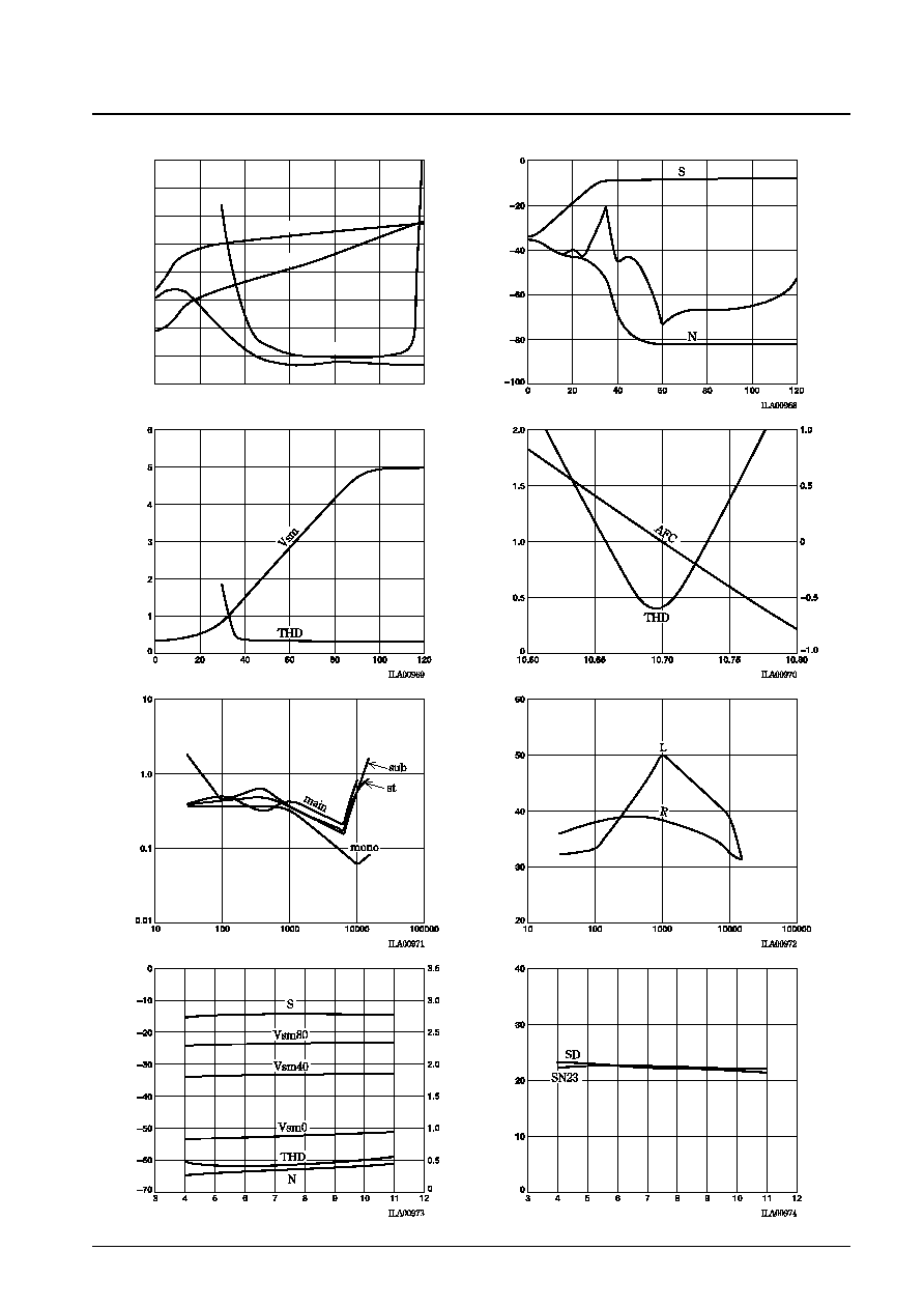
ILA00967
0
20
40
60
80
100
120
0
--10
--20
--30
--70
--40
--50
--60
10
0
1.5
1.0
0.5
2.0
2.5
4.0
3.5
3.0
S
Vsm
THD
N
AM
AM Input/Output Characteristics
FM Input/Output Characteristics 2
Multiplex Frequency Characteristics 1
AM Supply Voltage Characteristics 1
AM Supply Voltage Characteristics 2
Multiplex Frequency Characteristics 2
FM Detuning Characteristics
FM Input/Output Characteristics 1
Output voltage, V
O
-- dBV
S-meter voltage, Vsm -- V
Total harmonic distortion, THD -- %
Total harmonic distortion, THD -- %
Output voltage, V
O
-- dBV
Signal-to-noise ratio, SN -- dB
Channel separation, Sep -- dB
Channel separation, Sep -- dB
AFC voltage, Vafc -- V
Total harmonic distortion, THD -- %
Output voltage, V
O
-- dBV
Total harmonic distortion, THD -- %
S-meter voltage, Vsm -- V
Input, INPUT -- dB
µ
Input, INPUT -- dB
µ
Modulation frequency, fm -- Hz
Supply voltage, V
CC
-- V
Supply voltage, V
CC
-- V
Modulation frequency, fm -- Hz
Frequency, fc -- MHz
Input, INPUT -- dB
µ

No. 5888-8/10
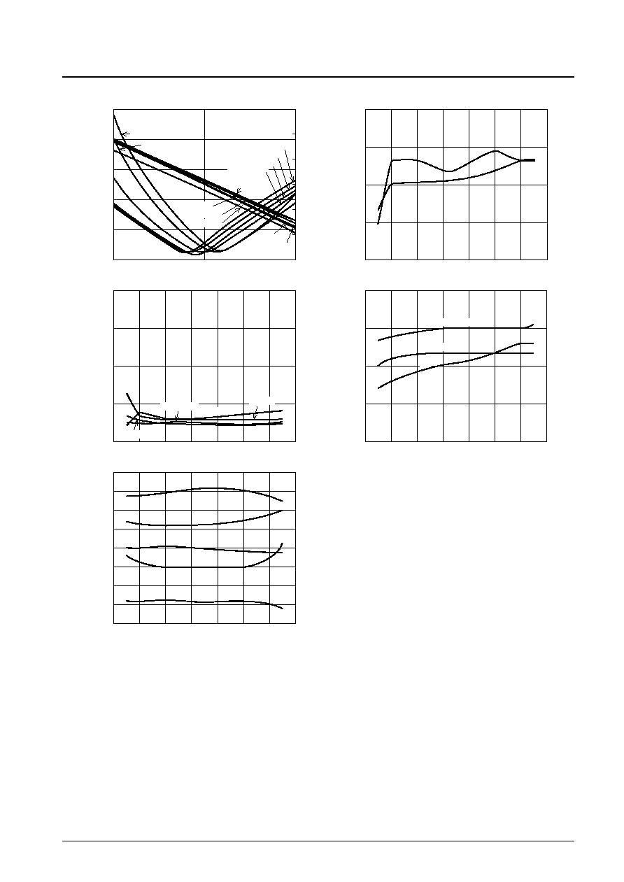
LA1845N, 1845NM
ILA00975
3
4
6
5
7
8
9
10
11
12
--10
--20
--30
--40
--50
--60
--90
--70
--80
0
0
3
2
1
4
5
6
7
8
9
S
Vsm100
Vsm70
Vsm0
THD
AM
N
ILA00976
3
4
6
5
7
8
9
10
11
12
30
20
10
50
40
LS
SD
ILA00979
--40
--20
0
20
40
60
80
100
--20
--40
--60
--80
0
0
1.0
0.5
1.5
2.0
2.5
3.0
S
Vsm80
Vsm40
Vsm0
THD
N
ILA00977
2
4
6
8
10
12
50
40
30
20
0
10
60
0
3
2
1
4
5
6
SepL
SepR
Vlon
Vloff
ILA00978
2
4
6
8
10
12
10
8
6
4
0
2
12
THDmain
THDst
THDsub
ILA00981
--40
--20
0
20
40
60
80
100
--20
--40
--60
--100
--80
0
0
2
1
3
4
5
6
S
Vsm100
Vsm70
THD
N
AM
ILA00980
--40
--20
0
20
40
60
80
100
30
20
10
0
40
SN23
SD
Vsm0
ILA00982
--40
--20
0
20
40
60
80
100
40
30
10
20
50
SD
LS
FM Supply Voltage Characteristics 1
FM Supply Voltage Characteristics 2
Multiplex Supply Voltage Characteristics 2
AM Temperature Characteristics 2
FM Temperature Characteristics 2
Multiplex Supply Voltage Characteristics 1
AM Temperature Characteristics 1
FM Temperature Characteristics 1
Output voltage, V
O
-- dBV
Channel separation, Sep -- dB
Output voltage, V
O
-- dBV
Output voltage, V
O
-- dBV
Sensitivity, Sens -- dB
µ
Sensitivity, Sens -- dB
µ
Sensitivity, Sens -- dB
µ
Total harmonic distortion, THD -- %
Total harmonic distortion, THD -- %
S-meter voltage, Vsm -- V
ST sensitivity, VL -- %
Total harmonic distortion, THD -- %
S-meter voltage, Vsm -- V
Supply voltage, V
CC
-- V
Supply voltage, V
CC
-- V
Supply voltage, V
CC
-- V
Supply voltage, V
CC
-- V
Ambient temperature, Temp --
∞
C
Ambient temperature, Temp --
∞
C
Ambient temperature, Temp --
∞
C
Ambient temperature, Temp --
∞
C
No. 5888-9/10
LA1845N, 1845NM
ILA00983
10.6
10.7
10.8
4
3
2
0
1
5
--1.5
THD --25
∞
C
AFC --25
∞
C
AFC 0
∞
C
AFC 50
∞
C
AFC 75
∞
C
AFC 25
∞
C
AFC 95
∞
C
THD 0
∞
C
THD 25
∞
C
THD 50
∞
C
THD 95
∞
C
THD 75
∞
C
ILA00984
--40
--20
0
20
40
60
80
100
50
40
20
30
60
SepL
SepR
ILA00985
--40
--20
0
20
40
60
80
100
0.5
1.5
0
2.0
1.0
ILA00986
--40
--20
0
20
40
60
80
100
70
60
50
90
80
S / Nmono
S / Nst
M Att
ILA00987
--40
--20
0
20
40
60
80
100
0
--4
--8
8
4
--2
--6
6
2
2.0
1.0
0
4.0
3.0
1.5
0.5
3.5
2.5
CR+
Vlon
fF
Vloff
CR--
THDmono
THDmain
THDst
THDsub
FM Temperature Characteristics 3
Total harmonic distortion, THD -- %
Input frequency, fc -- MHz
Multiplex Temperature Characteristics 2
Total harmonic distortion, THD -- %
Ambient temperature, Temp --
∞
C
Multiplex Temperature Characteristics 4
Free-running frequency drift,
f -- %
Capture range, CR -- %
ST sensitivity, VL -- %
Ambient temperature, Temp --
∞
C
Multiplex Temperature Characteristics 3
Signal-to-noise ratio, SN -- dB
Muting attenuation, Matt -- dB
Ambient temperature, Temp --
∞
C
Multiplex Temperature Characteristics 1
Channel separation, Sep -- dB
Ambient temperature, Temp --
∞
C
AFC voltage, Vafc -- mV
PS. No. 5888-10/10
LA1845N, 1845NM
This catalog provides information as of September, 2002. Specifications and information herein are
subject to change without notice.
Specifications of any and all SANYO products described or contained herein stipulate the performance,
characteristics, and functions of the described products in the independent state, and are not guarantees
of the performance, characteristics, and functions of the described products as mounted in the customer's
products or equipment. To verify symptoms and states that cannot be evaluated in an independent device,
the customer should always evaluate and test devices mounted in the customer's products or equipment.
SANYO Electric Co., Ltd. strives to supply high-quality high-reliability products. However, any and all
semiconductor products fail with some probability. It is possible that these probabilistic failures could
give rise to accidents or events that could endanger human lives, that could give rise to smoke or fire,
or that could cause damage to other property. When designing equipment, adopt safety measures so
that these kinds of accidents or events cannot occur. Such measures include but are not limited to protective
circuits and error prevention circuits for safe design, redundant design, and structural design.
In the event that any or all SANYO products (including technical data, services) described or contained
herein are controlled under any of applicable local export control laws and regulations, such products must
not be exported without obtaining the export license from the authorities concerned in accordance with the
above law.
No part of this publication may be reproduced or transmitted in any form or by any means, electronic or
mechanical, including photocopying and recording, or any information storage or retrieval system,
or otherwise, without the prior written permission of SANYO Electric Co., Ltd.
Any and all information described or contained herein are subject to change without notice due to
product/technology improvement, etc. When designing equipment, refer to the "Delivery Specification"
for the SANYO product that you intend to use.
Information (including circuit diagrams and circuit parameters) herein is for example only; it is not
guaranteed for volume production. SANYO believes information herein is accurate and reliable, but
no guarantees are made or implied regarding its use or any infringements of intellectual property rights
or other rights of third parties.