 | –≠–ª–µ–∫—Ç—Ä–æ–Ω–Ω—ã–π –∫–æ–º–ø–æ–Ω–µ–Ω—Ç: LA1867NM | –°–∫–∞—á–∞—Ç—å:  PDF PDF  ZIP ZIP |

Ordering number : EN4619B
32096HA (OT)/D2593TS (OT) No. 4619-1/32
Overview
The LA1867M is a high-performance multifunction (FM-
IF, noise canceller, MPX and MRC) single-chip tuner IC
for use in car radios. High-quality tuners with superlative
cost-performance characteristics can be constructed easily
using this IC.
Functions
∑ FM-IF
∑ Noise canceller
∑ MPX
∑ MRC (multipath noise reduction circuit)
Features
∑ Forms a high-performance FM tuner when combined
with the Sanyo LA1193 FM front-end IC.
∑ Multiple functions, MRC circuit, dual diversity, and
RDS handling
∑ High performance, high sensitivity and high stability
(excellent temperature characteristics)
∑ High audio quality and noise reduction according to the
reception conditions.
∑ Miniaturization of the required external capacitors
(electrolytic capacitors no longer required)
∑ Easy adjustment (The SD, muting and SNC circuits are
separated.)
Package Dimensions
unit: mm
3148-QIP44MA
SANYO: QIP44MA
[LA1867NM]
LA1867NM
SANYO Electric Co.,Ltd. Semiconductor Bussiness Headquarters
TOKYO OFFICE Tokyo Bldg., 1-10, 1 Chome, Ueno, Taito-ku, TOKYO, 110-8534 JAPAN
Car Radio Single-Chip Tuner System
Monolithic linear IC
Specifications
Maximum Ratings
at Ta = 25∞C
Operating Conditions
at Ta = 25∞C
Parameter
Symbol
Conditions
Rating
Unit
Maximum supply voltage
V
CC
max
Pins 4 and 31
9.2
V
Allowable power dissipation
Pdmax
740
mV
Operating temperature
Topr
≠40 to +85
∞C
Storage temperature
Tstg
≠40 to +150
∞C
Parameter
Symbol
Conditions
Rating
Unit
Recommended supply voltage
V
CC
Pins 4 and 31
8.0
V
V
CC ST/SD
Pins 29 and 44
5.0
V
Operating supply voltage range
V
CC
op
7.0 to 9.0
V
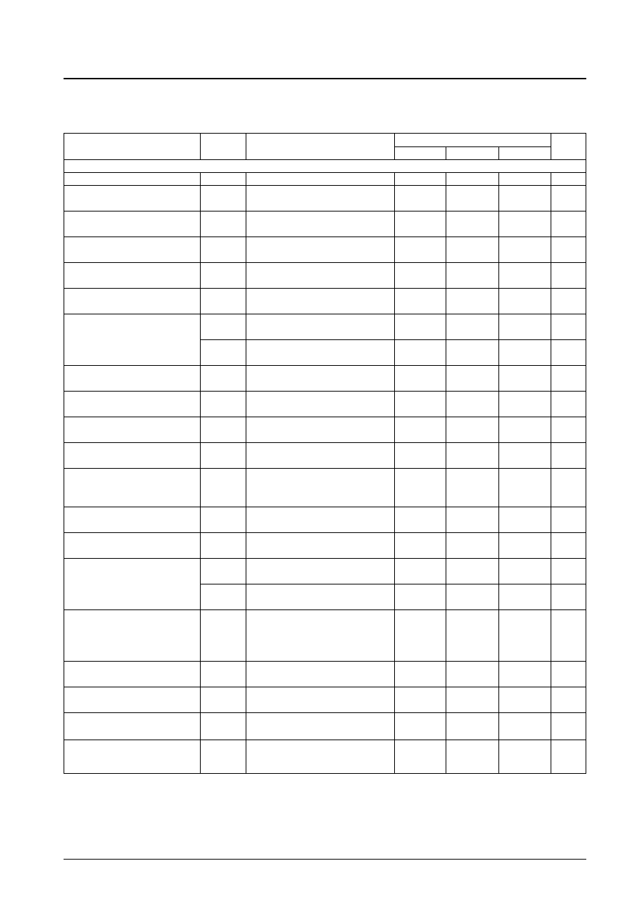
Operating Characteristics
at Ta = 25∞C, V
CC
= 8.5 V (Note that these measurements are made using
the IC-51-044-464 IC socket manufactured by Yamaichi Electric Works, Ltd.)
Note:
*
Unless otherwise specified, with an IHF-BPF/T200 inserted in the pin 7 and 8 MPX output circuit.
No. 4619-2/32
LA1867NM
Parameter
Symbol
Conditions
Rating
Unit
min
typ
max
[FM BLOCK]
Quiescent current
I
CCO-FM
No input (I
4
+ I
31
)
40
55
70
mA
Demodulator output
V
O-FM
10.7 MHz, 100 dBµ, 1 kHz,
175
260
350
mVrms
100% mod, pin 7 output
Channel balance
C
B
10.7 MHz,100 dBµ, 1 kHz, 100% mod, the
≠1.0
0
+1.0
dB
ratio of pin 7 to pin 8, Referenced to pin 7.
Total harmonic distortion
THD-
FMmono
10.7 MHz, 100 dBµ, 1 kHz,
0.2
1.0
%
100% mod, pin 7
Signal-to-noise ratio (IF)
S/N-
FM
IF
10.7 MHz,100 dBµ, 1 kHz,
73
80
dB
100% mod, pin 7
AM suppression ration (IF)
AMRIF
10.7 MHz,100 dBµ 1 kHz, fm = 1 kHz,
57
70
dB
Pin 7 when the AM modulation is 30%
Att-1
10.7 MHz, 100 dBµ, 1 k Hz, the pin 7
20
25
30
dB
attenuation when V
22
goes from 0 to 1 V
Muting attenuation
Att-2
10.7 MHz, 100 dBµ, 1 k Hz, the pin 7
28
33
38
dB
attenuation when V
22
goes from 0 to 2 V
Channel separation
Separation
10.7 MHz, 100 dBµ, L + R = 90%,
30
40
dB
pilot = 10%, the pin 7 output ratio
Stereo on level
ST-
ON
The pilot modulation level such that V
44
1.5
2.9
5.0
%
becomes less than 0.5 V
*
Stereo off level
ST-
OFF
The pilot modulation level such that V
44
0.8
1.9
%
becomes greater than 3.5 V
*
Total harmonic distortion
THD-
MainL
10.7 MHz, 100 dBµ, L + R = 90%,
0.3
1.0
%
pilot = 10%, pin 7
10.7 MHz, 100 dBµ, pilot = 10%,
Pilot cancellation
P
CAN
pin 7 signal/PILOT-LEVEL leakage,
20
35
dB
DIN-audio filter
SNC output voltage
V
OSUB
10.7 MHz, 100 dBµ, L ≠ R = 90%,
3
10
mVrms
pilot = 10%, V
13
= 0.1 V, pin 7
SNC output attenuation
Att
SNC
10.7 MHz, 100 dBµ, L ≠ R = 90%,
2
6
10
dB
pilot = 10%, V
13
= 3 V to 0.6 V, pin 7
Att
HCC-1
10.7 MHz, 100 dBµ, 10 kHz, L + R = 90 %,
2
6
10
dB
pilot = 10%, V
14
= 3 V to 0.6 V, pin 7
HCC output attenuation
Att
HCC-2
10.7 MHz,100 dBµ, 10 kHz, L + R = 90 %,
6
10
14
dB
pilot = 10%, V
14
= 3 V to 0.1 V, pin 7
10.7 MHz, 100dBµ, 100% mod, IF input
Input limiting voltage
Vi-lim
such that the input reference output is
33
42
51
dBµ
down by ≠3 dB, when the soft muting
function is operating
Muting sensitivity
Vi-Mute
The IF unmodulated input level when
32
40
48
dBµ
V
23
is 2 V.
SD sensitivity
SD
sen
The unmodulated IF input such that the SD
64
74
84
dBµ
pin voltage (V29) becomes 3.5 V or higher.
IF counter buffer output
V
IFBUFF-FM
10.7 MHz, 100 dBµ, unmodulated,
160
230
320
mVrms
the pin 19 output
AM output
V
O-AM
The pin 7 output in AM mode (AC
2
=
234
330
466
mVrms
300 mV rms, 1 kHz, the pin 20 input)
Continued on next page.

Continued from preceding page.
Block Functions
1. FM-IF
∑ IF-limiter amplifier
∑ S-meter outputs (three systems)
∑ Quadrature detector
∑ AF preamplifier
∑ AFC output
∑ Muting circuit (band mute, weak input mute, soft mute)
∑ Control pins (SD, muting attenuation, soft mute on level)
∑ SD output
∑ IF counter buffer output
∑ S-meter output shifter
2. Noise canceller
∑ Built-in high-pass filter
∑ Built-in low-pass filter delay circuit
∑ Noise AGC
∑ Pilot signal compensation circuit
∑ Noise reduction setting pin
∑ Noise canceller off in AM mode function
∑ High-pass filter "fc" control pin
No. 4619-3/32
LA1867NM
Parameter
Symbol
Conditions
Rating
Unit
min
typ
max
[FM BLOCK]
V
SMFM-1
No input, pin 32 DC output,
0.0
0.1
0.3
V
non-mod, SW-2 open
V
SMFM-2
50 dBµ, pin 32 DC output,
1.0
2.1
3.3
V
Signal meter output
non-mod, SW-2 open
V
SMFM-3
70 dBµ, pin 32 DC output,
2.3
3.5
5.3
V
non-mod, SW-2 open
V
SMFM-4
100 dBµ, pin 32 DC output,
4.7
6.0
6.7
V
non-mod, SW-2 open
Muting bandwidth
BW-Mute
100 dBµ, The bandwidth when V
23
= 2 V,
110
190
290
kHz
non-mod
Muting drive output
V
Mute-100
100 dBµ, pin 23 DC output, non-mod
0.00
0.03
0.20
V
[N.C BLOCK]
Noise Canceller Input (pin 20), PG1
f = 1 kHz, 1 µs, with a 100 mV p-o pulse
t
GATE
1
input, the time for V
40
to become 1 V
35
55
75
µs
or higher
Gate time
f = 1 kHz, 1 µs, with a 100 mV p-o pulse
t
GATE
2
input, with the MRC pin 15 input = 1 kHz,
10
25
40
µs
30 mV rms
With a 1 kHz signal such that the noise
Noise sensitivity
S
N
canceller operation is on, the 1 µs pulse
50
75
mVp-o
input level, measure pin 20.
[Multipath suppression circuit]
MRC Input (AC1)
MRC output
V
MRC
V
18
= 2 V, 1 kHz, 5 mV rms, the pin
1.75
1.85
1.95
V
12 voltage when there is a pin 15 input
MRC operating level
MRC-ON
V
18
= 2 V, the pin 15 input level such
15
30
mVrms
that V12 becomes 1.75 V

3. MPX
∑ Nonadjusting VCO (912 kHz)
∑ Level-following type pilot cancelation circuit
∑ SNC
∑ FM HCC
∑ Stereo/mono display output
∑ Built-in anti-birdie stereo decoder
∑ Automatic stereo/mono switching
4. MRC
∑ DC level shifter circuit
∑ Noise amplifier
∑ Noise detection circuit
∑ Time constant control circuit
Block Features
1. FM-IF
∑ The development of a high performance S-meter circuit has simplified all types of control.
-- High linearity S-meter circuit (6-stage detection type)
-- High quality S-meter (superlative temperature characteristics)
∑ High quality design
-- Design that emphasizes temperature characteristics
-- S-meter, SD sensitivity, ≠3 dB L.S., etc.
∑ Improved active characteristics
-- Muting circuit time constant control (Since the attack and recovery time can be set independently, the audio
quality under multipath conditions can be improved.)
-- Three built-in S-meter circuits
Soft mute/H
CC
time constants
SD time constants
Application design is eased since these can all be set independently.
SNC time constants
2. Noise canceller
∑ Noise canceller error prevention when a narrow band (150 kHz) ceramic filter is used
∑ A new noise canceller system was developed.
-- Reduced noise canceller errors during overmodulated signal reception.
-- Reduced noise canceller errors under continuous noise conditions.
∑ Miniaturization of the required external capacitors
No. 4619-4/32
LA1867NM

3. MPX
∑ Miniaturization of the required external components (nonadjusting 912 kHz VCO)
∑ Improved basic performance
-- Pilot cancelation level (30 dB typ.)
-- No variation in mono output level due to separation adjustment (subcarrier output level adjustment type
separation adjustment)
-- A new SNC curve was developed.
-- Built-in anti-birdie filters (114 kHz and 190 kHz)
-- Improved high region separation characteristics
-- Improved stereo signal-to-noise ratio
4. MRC
∑ Controls the SNC and HCC circuit control signals by detecting the field strength (S-meter) and multipath noise.
No. 4619-5/32
LA1867NM

Test Circuit
No. 4619-6/32
LA1867NM
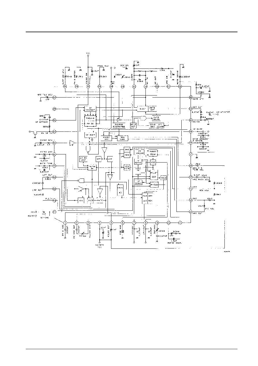
Block Diagram and Peripheral Circuits
No. 4619-7/32
LA1867NM
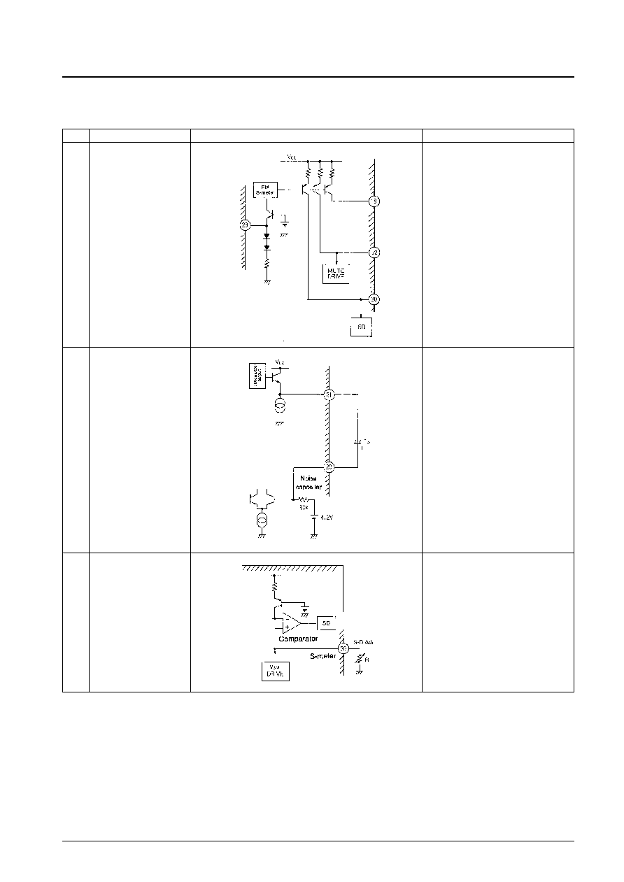
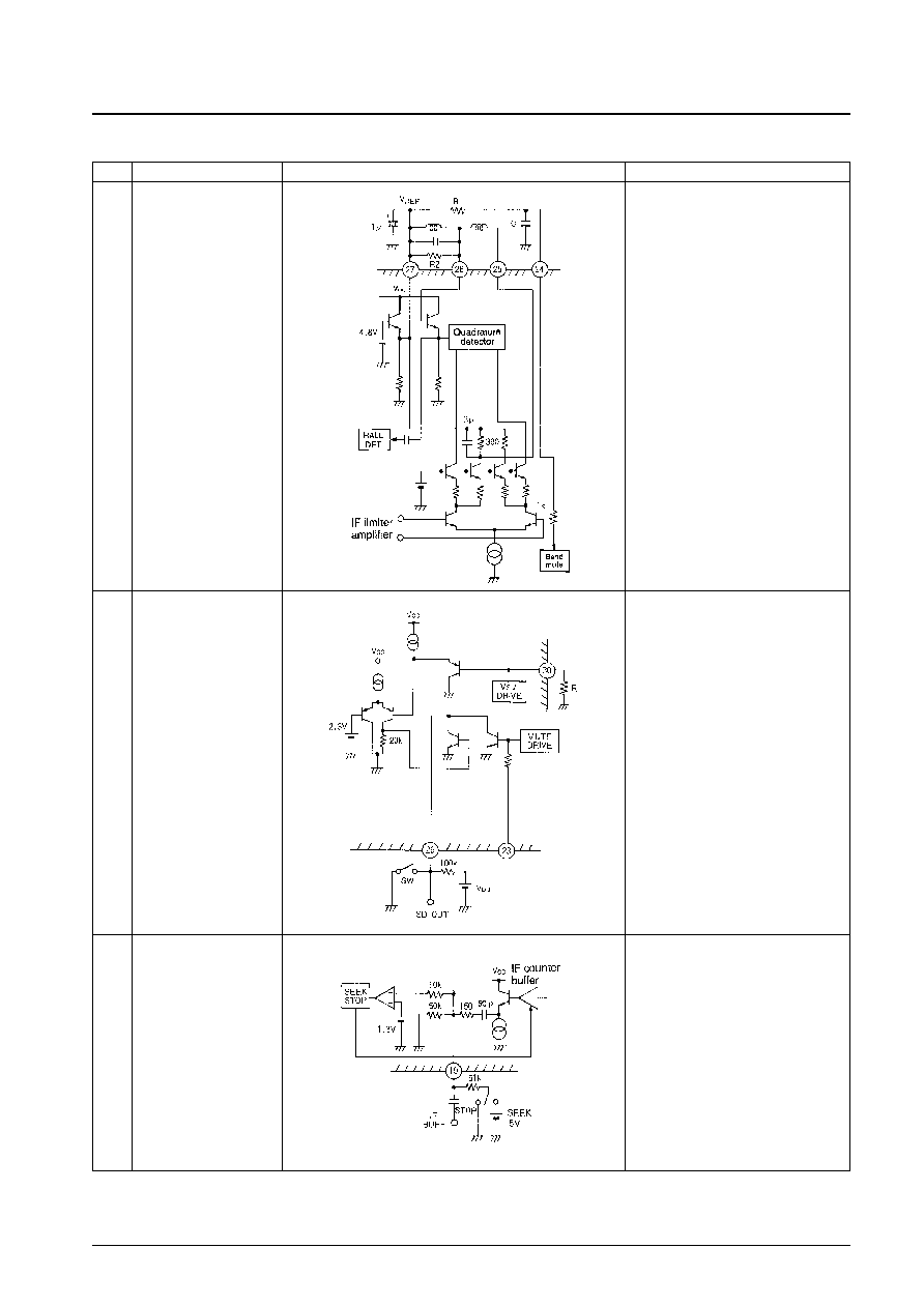
Pin Functions
FM-IF Block
No. 4619-8/32
LA1867NM
Continued on next page.
Pin
Function
Equivalent internal circuit
Note
18
S-meter output for MRC
and SNC
32
S-meter output for muting
drive and HCC
30
S-meter output for SD
28
S-meter output shift control
pin
20
Noise canceller input
21
FM detector output
30
FM SD Adj
Constant current drive type
The slope can be changed by changing the
value of the S-meter output resistance.
The field strength can be shifted in the
positive or negative direction with an
external resistor on pin 28 without changing
the S-meter slope.
Noise canceller input
The input impedance is 50 k
.
FM detector output
Low impedance in FM mode
Pin 30
The comparison voltage is determined by
the external resistor.
Pin 30 is the S-meter output, and SD turns
on when it exceeds the internal supply
voltage.
Unit (resistance:
, capacitance:F)
Continued from preceding page.
No. 4619-9/32
LA1867NM
Continued on next page.
Pin
Function
Equivalent internal circuit
Note
37
FM IF IN
36
IF BYPASS
23
Mute drive output
22
Mute input
33
FM mute ON Adj
Limited amplifier input
Select the capacitor grounding point
carefully.
The muting time constants from the
external CR circuit are determined as
follows.
Attack time T
A
= R
1
◊
C
2
Release time T
R
= R
2
◊
C
2
Noise convergence adjustment
Divide the V
23
voltage by R
2
when
there is no input at the antenna input,
and input that voltage to pin 22.
Noise convergence will be maximum
when V
22
= 2 V.
The variation range is 5 to 35 dB,
taking the 1 kHz 22.5 kHz dev output
as the reference.
Muting off function
The muting is turned off when pin 22 is
shorted to ground.
The muting on level is adjusted by changing
the external resistance R.
Unit (resistance:
, capacitance:F)
Continued from preceding page.
No. 4619-10/32
LA1867NM
Pin
Function
Equivalent internal circuit
Note
24
AFC
25
QD OUT
26
QD IN
27
V
REF
29
SD pin
30
SD sensitivity adjustment
pin
19
IF counter buffer
Seek/stop switch
∑ R
1
is the resistor that determines the band
muting bandwidth.
Increasing R
1
reduces the bandwidth.
Decreasing R
1
increases the bandwidth.
∑ Null voltage
When tuned, the voltage between pins 24
and 27 will be 0 V.
V
24
≠ V
27
= 0 V
The band muting is turned on when
| V
24
≠ V
27
|
0.7 V.
The SD output for the pin 30 SD.
R determines the SD sensitivity.
Pin 23 is coupled to the muting drive output.
SD operates when the switch is off.
This pin is used for both the IF counter
buffer (AC output) and the seek/stop switch
(DC input).
It is not coupled to the SD output.
The IF buffer is turned on and off by the pin
19 DC bias level.
Pin 19: high
buffer on, low
buffer off.
Unit (resistance:
, capacitance:F)
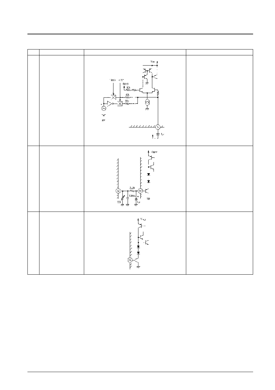
MPX Block
No. 4619-11/32
LA1867NM
Continued on next page.
Pin
Function
Equivalent internal circuit
Note
5
Pilot detector
14
H
CC
control input pin
13
SNC control input pin
The IC is forced to mono if a 1 M
resistor
is inserted between pin 5 and V
CC
.
H
CC
is off in AM mode.
Controls the sub output with an input of
between 0 and 1 V.
Unit (resistance:
, capacitance:F)

Continued from preceding page.
No. 4619-12/32
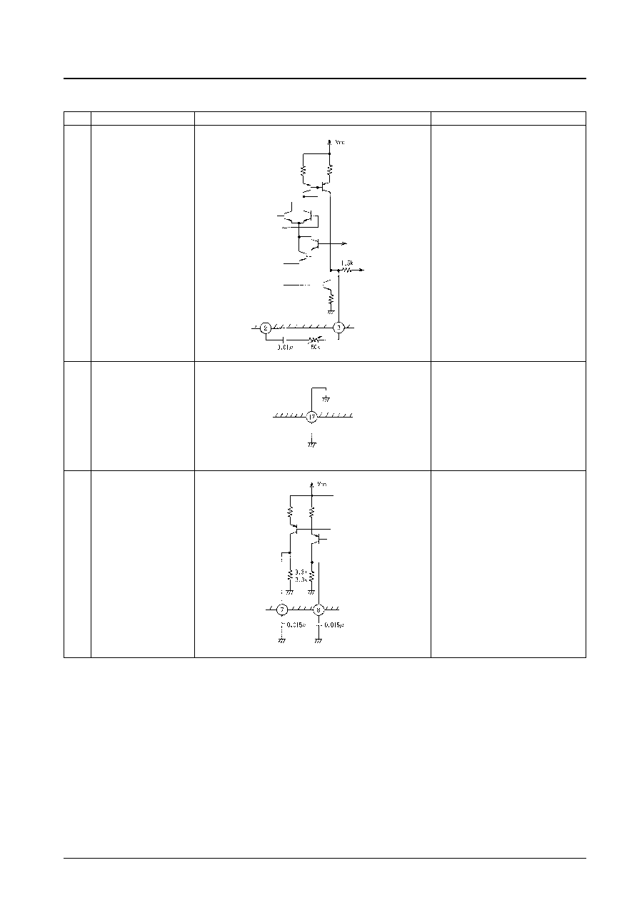
LA1867NM
Continued on next page.
Pin
Function
Equivalent internal circuit
Note
10
PHASE COMP.
11
9
Separator adjustment pin
6
VCO
The sub decoder input level is adjusted with
a trimmer.
(The output level in mono and main modes
does not change.)
The oscillator frequency is 912 kHz.
Unit (resistance:
, capacitance:F)
Continued from preceding page.
No. 4619-13/32
LA1867NM
Pin
Function
Equivalent internal circuit
Note
3
Pilot cancellation signal
output
17
GND
7
MPX out (left)
8
MPX out (right)
Pin 3 is the pilot cancellation signal output.
GND
Unit (resistance:
, capacitance:F)
MPX Block Applications
NC Block
No. 4619-14/32
LA1867NM
Continued on next page.
Pin
Function
Equivalent internal circuit
Note
43
Pilot input
1
HCC capacitor
Pin 43 is the PLL circuit signal input.
The HCC frequency characteristics are
determined by the capacitor connected at
this pin.
Pin
Function
Equivalent internal circuit
Note
2
Pilot cancellation signal
input
The pilot signal level must be adjusted since
it varies with manufacturing variations in the
IF output level and other parameters.
Unit (resistance:
, capacitance:F)

Continued from preceding page.
NC Block Applications
No. 4619-15/32
LA1867NM
Continued on next page.
Pin
Function
Equivalent internal circuit
Note
Time constant connection
40
for the monostable
multivibrator
41
42
Memory circuit pins
43
This time constant sets the gate time to 40 µs.
The noise rejection ratio increases with the
gate time. However, caution is required
since multipath and the distortion sensitivity
for overmodulated signals are degraded.
The memory circuit used when the noise
canceller operates
Pin
Function
Equivalent internal circuit
Note
20
Noise killer input
The input impedance is about 50 k
.
Unit (resistance:
, capacitance:F)

Continued from preceding page.
MRC Block
No. 4619-16/32
LA1867NM
Pin
Function
Equivalent internal circuit
Note
38
Noise AGC sensitivity
39
adjustment pins
35
HPF slope adjustment pin
Pin 38 is the noise sensitivity setting pin.
First set the medium field (about 50 dBµ)
level, and the set the weak field (about 20 to
30 dBµ) with pin 39 (AGC adjustment).
The slope of the high-pass filter can be
adjusted by changing the value of the
resistor (R) connected between pin 35 and
ground. If this adjustment is not needed,
pin 35 can be left open.
Pin
Function
Equivalent internal circuit
Note
18
IF S-meter output and MRC
DC input pin
S-meter output block
MRC DC input block
Continued on next page.
Unit (resistance:
, capacitance:F)

Continued from preceding page.
MRC Block Applications
No. 4619-17/32
LA1867NM
Pin
Function
Equivalent internal circuit
Note
12
MRC output pin
Pin
Function
Equivalent internal circuit
Note
34
MRC control voltage time
constant
15
MRC AC input pin
34
MRC control voltage time
constant
16
Time constant setting pin
constant
In methods in which the S-meter AC
components are detected directly, the noise
amplifier gain is determined by R
2
and the
30 k
internal resistance, as shown in
Figure 1. A certain degree of filtering
characteristics can be provided with
capacitor C
1
.
In methods in which the S-meter high area
components are detected, or the NC HDF
noise output is detected, the noise amplifier
gain is determined by R
2
and 30 k
as
shown in Ffigure 2. Here, the frequency
characteristics are determined by C
1
.
During discharge, the MRC detector time
constant is determined by R
S
(1 k
) and
C
A
. During charge, it is determined by I
C
and C
A
.
Attack time = C
A
◊
R
S
(Stereo
mono)
Recovery time = C
A
◊
R
A
(Mono
stereo)
Unit (resistance:
, capacitance:F)
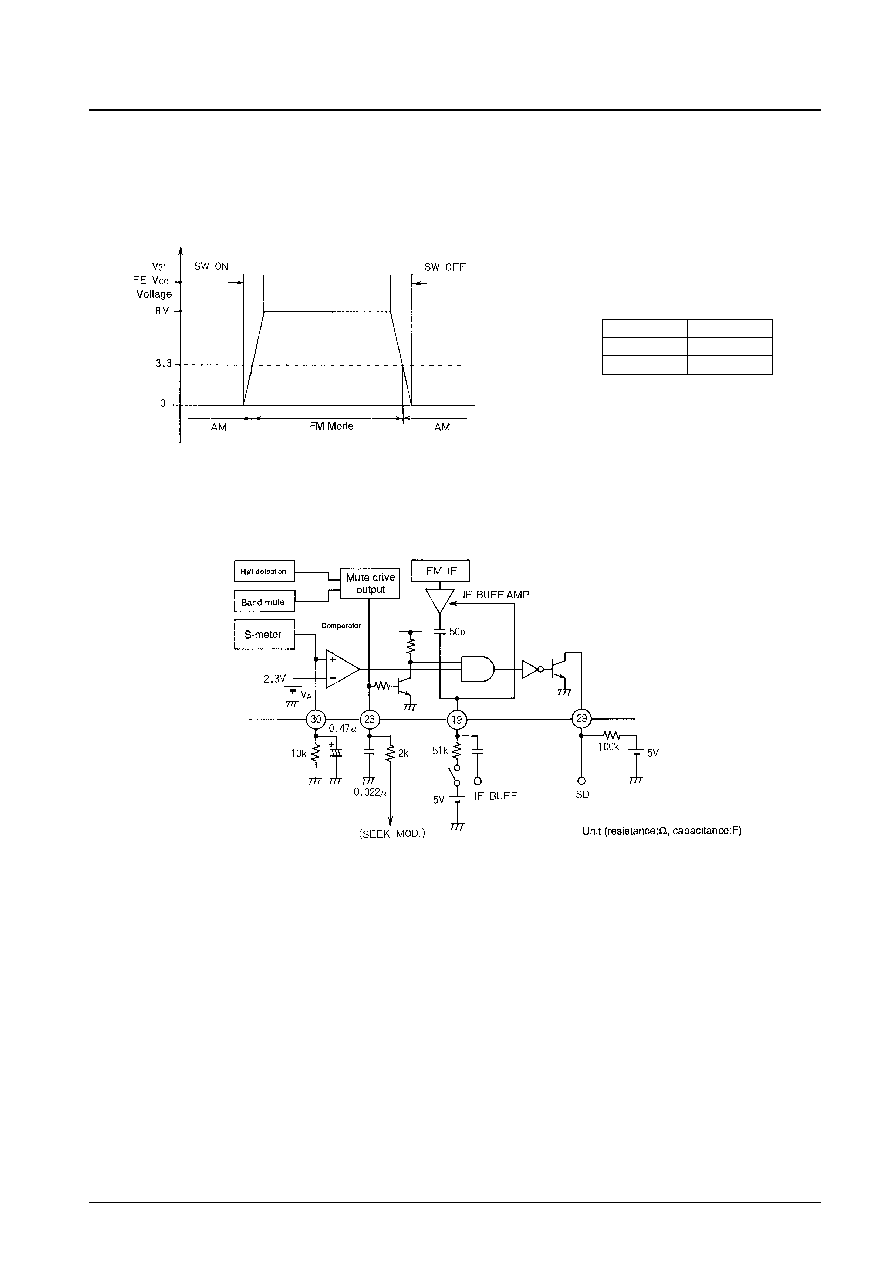
Usage Notes
1. AM/FM switching: Pin 31 (IF V
CC
)
This pin is shared with the IF V
CC
. When the FM IF is operated, the IC automatically switches to FM mode. (Note
that the switching reference voltage is 3.3 V.)
Figure 1
2. FM SD and SD adjustment
The FM SD and the IF counter buffer operate with the elements shown below.
The following conditions are required for FM SD operation.
∑ V
30
> V
A
:
The S-meter voltage must be higher than the regulator voltage.
∑ V
23
< 0.7 V (V
BE
): The Hall detector and band mute must not operate.
∑ V
29
= H:
A high level must be applied to pin 29 through a 100 k
resistance.
The following condition is required for IF buffer operation.
∑ V
19
= H:
A high level must be applied to pin 19 through a 51 k
resistance.
No. 4619-18/32
LA1867NM
Pin V
31
Mode
8 V
FM
open
AM
3. FM muting on: Pin 33 (R33 = 100 k
)
The ≠3 dB limiting sensitivity can be changed by varying R
33
.
(Currently, R33 is 25 k
to set the ≠3 dB limiting sensitivity to 8 dBµ.)
4. FM muting attenuation adjustment: Pin 22 (R22 is a 30 or 50 k
variable resistor)
The pin 23 voltage is divided by the R
22
variable resistor and input to pin 22. The no-input noise convergence is
determined by value of the pin 22 voltage.
(The LA1867NM has a noise convergence design target of from 5 dB to 30 dB.)
5. Muting time constant
The LA1867NM allows the volume level to be changed gradually for field variations during weak field reception by
setting the attack and recovery times for the soft mute function.
6. FM mute off function
The muting function is turned off if pin 22 is forcibly connected to ground.
No. 4619-19/32
LA1867NM
Attack time setting
ta = R
23
*
C
22
= 940 µsec
Recovery time setting
tr = C
22
*
R
23
= 23500 µsec
Unit (resistance:
, capacitance: F)
MPX Block
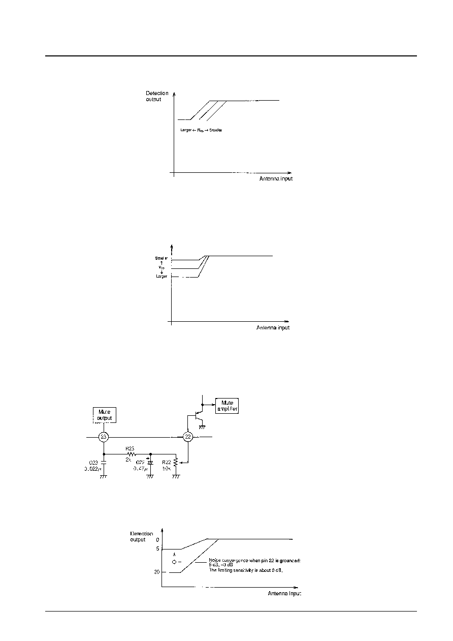
1. HCC (high-cut control frequency characteristics (pin 1)
During HCC control, the output signal frequency characteristics are determined by the capacitance of the external
capacitor connected to pin 1.
2. Pilot cancellation adjustment (pins 2 and 3)
The pin 3 pilot cancellation waveform is a 19 kHz signal that does not include a third upper harmonic component, as
shown in the figure above. Also, no capacitor is required between pin 3 and ground since this signal is in phase with
the pilot signal. Good pilot cancellation characteristics can be acquired in the left and right channels by adjusting the
variable resistor, since the signal does not include a third upper harmonic component.
3. Separation adjustment (pin 9)
The separation is adjusted by varying the sub-decoder input level with the pin 9 variable resistor. Only the sub-decoder
level changes when the variable resistor is changed; the mono (main) output level does not change. Also, the decoder
high-band separation in the sub signal frequency band (23 to 53 kHz) will not degraded if the external capacitor C's
value is made sufficiently smaller than the variable resistor's impedance.
No. 4619-20/32
LA1867NM
Notes on Using the Application Circuits
1. NC Block
∑ The input impedance of the noise canceller input is about 50 k
. Carefully consider the low area frequency
characteristics when determining the value of the coupling capacitor. Note that when the value is 1 µF in the
application circuit, fc will be about 3 Hz.
∑ Pins 38 and 39 are used to set the noise detection sensitivity and the noise AGC.
The values of the external components can be determined more easily by first setting the medium field (antenna
input levels of about 50 dBµ) with the noise sensitivity setting pin (pin 38), and then setting the weak field (antenna
input levels of about 20 to 30 dBµ) with the AGC adjustment pin (pin 39). Care is required in determining these
settings since while the AGC operation improves as the noise detection sensitivity is increased, inversely, the weak
field sensitivity decreases.
∑ If noise is detected again during gating, since the monostable multivibrator will be reset, the gate time will change
with the magnitude of the noise. Finally, set the gate time from the point noise is detected. When the circuit
constants in the circuit connected to pin 40 are C = 0.001 µF and R = 12 k
, the gate time will be about 10 µs.
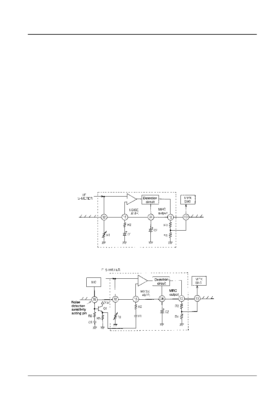
2. MRC Block
∑ The MRC (multipath rejection circuit) supports three techniques as shown in Figures 2, 3 and 4. Figure 2 shows the
technique in which the S-meter AC component is detected directly. Figure 3 shows the technique in which the NC
HPF noise is detected, and Figure 4 shows the technique in which multipath is detected using the S-meter high area
components.
Figure 2 Multipath Circuit
Figure 3 Application Circuit Using NC HPF Noise Detection
No. 4619-21/32
LA1867NM
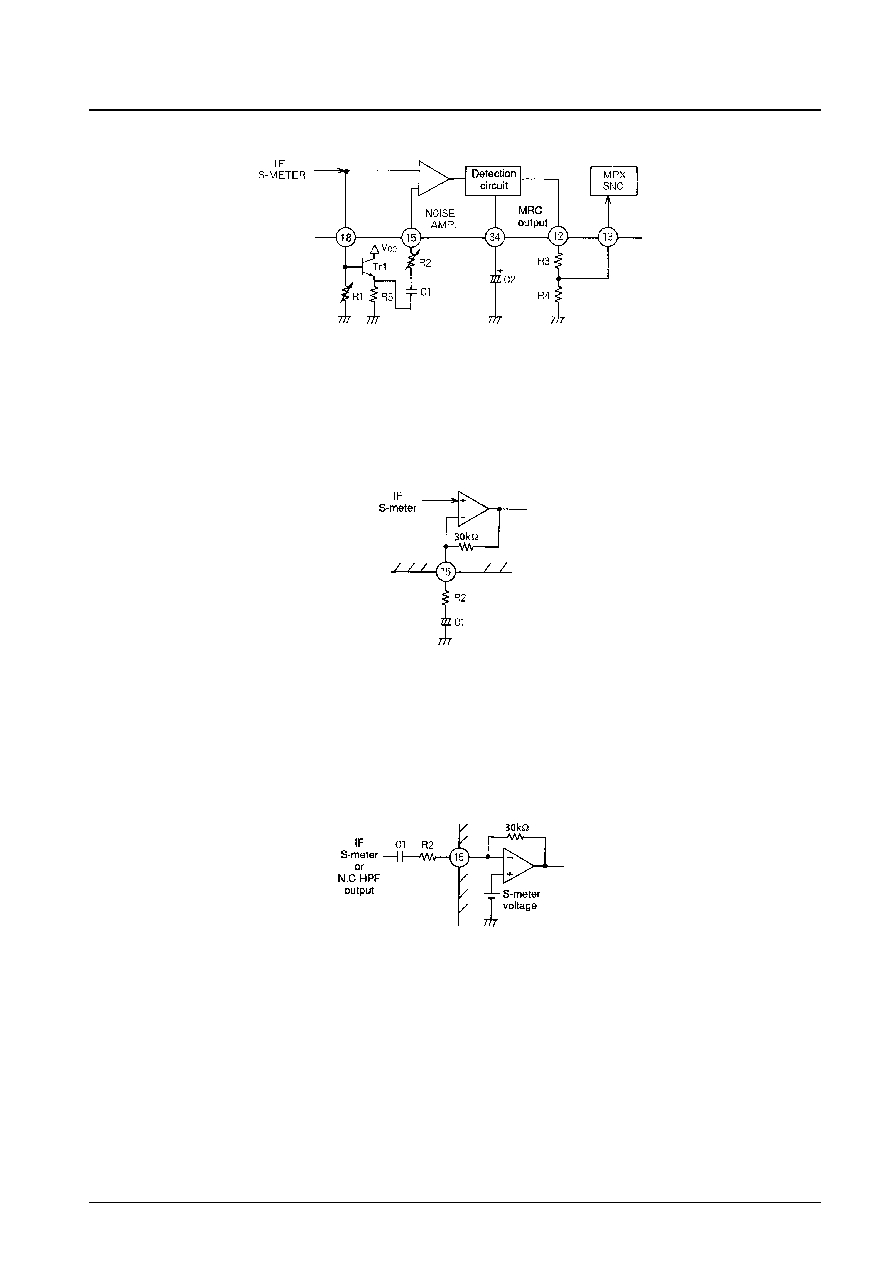
Figure 4 Application Circuit Using IF S-Meter High-Area Detection
∑ In the technique in which the S-meter AC component is detected directly the noise amplifier gain is determined by
R
2
and the internal 30 k
resistance as shown in Figure 5. A certain degree of filtering characteristics can be
provided with capacitor C
1
.
Figure 5
∑ In the technique of Figure 4, in which multipath is detected using the S-meter high area components, and In the
technique of Figure 3, in which the NC HPF noise is detected, the noise amplifier gain is determined by R
2
and the
internal 30 k
resistance as shown in Figure 6. The frequency characteristics of the circuit are determined by the
capacitor C
1
.
Figure 6
No. 4619-22/32
LA1867NM
∑ The time constants with which the MRC controls the separation are determined by the internal 1 k
resistance and
C
2
on discharge, and the 7 µA fixed current and C
2
on charge.
Coil Specifications
∑ Toko Electric Corporation Coils
7KLS M402AES-1298
∑ Sumida Electric Coils
QU-7L SA-208
∑ Ceramic Oscillators
∑ Murata Mfg. Co., Ltd.
CSB912JF104
No. 4619-23/32
LA1867NM
Figure 7
Figure 8
6-4
4T
6-3
22 1/4T
3-1
65T
C
91 pF
Q
30
4-3
18 1/4T
3-1
70 1/4T
C
100 pF
Q
35

No. 4619-24/32
LA1867NM
No. 4619-25/32
LA1867NM
No. 4619-26/32
LA1867NM
No. 4619-27/32
LA1867NM
No. 4619-28/32
LA1867NM

No. 4619-29/32
LA1867NM

No. 4619-30/32
LA1867NM

No. 4619-31/32
LA1867NM

No. 4619-32/32
LA1867NM
This catalog provides information as of February, 1997. Specifications and information herein are subject to
change without notice.
s
No products described or contained herein are intended for use in surgical implants, life-support systems, aerospace
equipment, nuclear power control systems, vehicles, disaster/crime-prevention equipment and the like, the failure of
which may directly or indirectly cause injury, death or property loss.
s
Anyone purchasing any products described or contained herein for an above-mentioned use shall:
Accept full responsibility and indemnify and defend SANYO ELECTRIC CO., LTD., its affiliates, subsidiaries and
distributors and all their officers and employees, jointly and severally, against any and all claims and litigation and all
damages, cost and expenses associated with such use:
Not impose any responsibility for any fault or negligence which may be cited in any such claim or litigation on
SANYO ELECTRIC CO., LTD., its affiliates, subsidiaries and distributors or any of their officers and employees
jointly or severally.
s
Information (including circuit diagrams and circuit parameters) herein is for example only; it is not guaranteed for
volume production. SANYO believes information herein is accurate and reliable, but no guarantees are made or implied
regarding its use or any infringements of intellectual property rights or other rights of third parties.