 | –≠–ª–µ–∫—Ç—Ä–æ–Ω–Ω—ã–π –∫–æ–º–ø–æ–Ω–µ–Ω—Ç: LA2655V | –°–∫–∞—á–∞—Ç—å:  PDF PDF  ZIP ZIP |
Any and all SANYO products described or contained herein do not have specifications that can handle
applications that require extremely high levels of reliability, such as life-support systems, aircraft's
control systems, or other applications whose failure can be reasonably expected to result in serious
physical and/or material damage. Consult with your SANYO representative nearest you before using
any SANYO products described or contained herein in such applications.
SANYO assumes no responsibility for equipment failures that result from using products at values that
exceed, even momentarily, rated values (such as maximum ratings, operating condition ranges,or other
parameters) listed in products specifications of any and all SANYO products described or contained
herein.
Monolithic Linear IC
Clear Sound Control IC
Loading "Plus Sound
Æ
" Algorithm
Ordering number:ENN6743
LA2655V
SANYO Electric Co.,Ltd. Semiconductor Company
TOKYO OFFICE Tokyo Bldg., 1-10, 1 Chome, Ueno, Taito-ku, TOKYO, 110-8534 JAPAN
73101TN (KT) No.6743≠1/4
1
10
11
6.4
6.5
0.5
4.4
0.1
1.5max
20
0.65
0.22
(0.33)
0.15
(1.3)
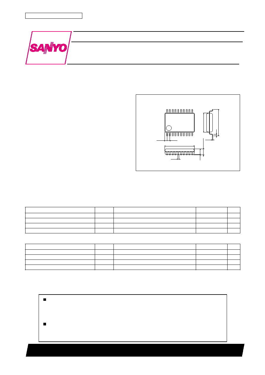
Package Dimensions
unit:mm
3179B-SSOP20
[LA2655V]
SANYO : SSOP20
Overview
The LA2655V is an IC for the sound replay which can be
used for the audio equipment such as the radio cassette re-
corder, the personal computer, the stereo, and the televi-
sion.
This IC has the function to replay a clear sound.
Features
Provides improved audio quality from one-way speaker
systems by incorporating the SANYO algorithm "Plus
Sound
Æ
", which corrects delay and attenuation differences
between high and low frequencies due to the characteris-
tics of the speaker.
Functions
∑ "Plus Sound
Æ
" algorithm provided on chip.
∑ Clear sound signal processing.
∑ Variable effect level (with external parts).
∑ Effect ON/OFF switch.
Specifications
Absolute Maximum Ratings
at Ta = 25∞C
∞C
∞C
Operating Conditions
at Ta = 25∞C
r
e
t
e
m
a
r
a
P
l
o
b
m
y
S
s
n
o
i
t
i
d
n
o
C
s
g
n
i
t
a
R
t
i
n
U
e
g
a
t
l
o
v
y
l
p
p
u
s
m
u
m
i
x
a
M
V C
C
x
a
m
3
1
V
n
o
i
t
a
p
i
s
s
i
d
r
e
w
o
p
e
l
b
a
w
o
ll
A
x
a
m
d
P
0
5
1
W
m
e
r
u
t
a
r
e
p
m
e
t
g
n
i
t
a
r
e
p
O
r
p
o
T
0
7
+
o
t
5
2
≠
e
r
u
t
a
r
e
p
m
e
t
e
g
a
r
o
t
S
g
t
s
T
5
2
1
+
o
t
0
4
≠
r
e
t
e
m
a
r
a
P
l
o
b
m
y
S
s
n
o
i
t
i
d
n
o
C
s
g
n
i
t
a
R
t
i
n
U
e
g
a
t
l
o
v
y
l
p
p
u
s
d
e
d
n
e
m
m
o
c
e
R
V C
C
0
.
9
V
e
g
n
a
r
e
g
a
t
l
o
v
y
l
p
p
u
s
g
n
i
t
a
r
e
p
O
V C
C
p
o
0
.
2
1
o
t
5
.
4
V
e
g
a
t
l
o
v
l
e
v
e
l
-
h
g
i
h
t
u
p
n
I
V H
I
V
o
t
5
.
2
C
C
V
e
g
a
t
l
o
v
l
e
v
e
l
-
w
o
l
t
u
p
n
I
V L
I
5
.
1
o
t
0
V
Ta
70∞C

LA2655V
No.6743≠2/4
Electrical Characteristics
at Ta = 25∞C, V
CC
=9V, fm=1kHz, Vin=300mVrms=0dB, R
L
=10k
Block Diagram
r
e
t
e
m
a
r
a
P
l
o
b
m
y
S
s
n
o
i
t
i
d
n
o
C
s
g
n
i
t
a
R
t
i
n
U
n
i
m
p
y
t
x
a
m
t
n
a
r
r
u
c
t
n
e
c
s
e
i
u
Q
T
c
c
I
s
s
a
p
y
b
,
l
a
n
g
i
s
o
N
5
0
1
A
m
n
o
i
t
a
i
v
e
d
l
e
v
e
l
t
u
p
t
u
O
T
G
V
s
s
a
p
y
B
2
≠
0
2
+
B
d
C
G
V
N
O
1
≠
1
+
3
+
B
d
e
g
a
t
l
o
v
t
u
p
t
u
o
m
u
m
i
x
a
M
T
x
a
m
o
V
s
s
a
p
y
B
5
.
1
2
s
m
r
V
C
x
a
m
o
V
N
O
5
.
1
2
s
m
r
V
n
o
i
t
r
o
t
s
i
d
c
i
n
o
m
r
a
h
l
a
t
o
T
T
D
H
T
s
s
a
p
y
B
5
0
0
.
0
3
0
.
0
%
C
D
H
T
N
O
8
0
.
0
5
.
0
%
e
g
a
t
l
o
v
e
s
i
o
n
t
u
p
t
u
O
T
o
n
V
s
s
a
p
y
B
5
9
≠
m
B
d
C
o
n
V
N
O
5
8
≠
m
B
d
P1
Mode
L
I/O through
H
effect
High level
R1, R3
Remarks
Max
≠
Mid
18k
Min
11k
Low level
R2, R4
Remarks
Max
10k
Mid
24k
Min
≠
19
18
11
12
13
14
15
16
17
2
3
10
9
8
7
6
5
4
L-ch control box
ON/OFF
control
Lch-IN
Rch-IN
Lch-OUT
Rch-OUT
Vcc
CONT1
GND
VREF
R-IN
RC1
RC2
RC3
R-OU T
1
20
RV1
RV2
+
C1
4.7
µ
F
C2
1
µ
F
C3
2200pF
C4
R1
2200pF
Vcc
AGND
L- IN
LC1
LC2
LC3
L-OUT
N.C
LV1
LV2
C5
82000pF
R2
+
+
+
+
+
+
C6
1
µ
F
1
µ
F
2200p
1
µ
F
4.7
µ
F
82000pF
R4
C12
C8
C7
C9
C10
C11
R3
C13
2200p
F
47
µ
F
L/H
SW
B
A
A
SW
B
R-ch control box

LA2655V
No.6743≠3/4
Pin Function
Pin No.
Pin Name
Pin Voltage
Description
Equivalent circuit
1
CONT1
0/5V
The function switching switch.
4
17
R-IN
L-IN
1/2VCC
The linear system input terminal.
5
16
RC1
LC1
1/2VCC
The terminal which connects the capacitor which
sets a phase shift position with the high frequency.
6
15
RV1
LV1
1/2VCC
It connects resistance and a capacitor to amplify
the high frequency.
7
14
RC2
LC2
1/2VCC
The terminal which connects the capacitor which
sets a phase shift position with the low frequency.
8
13
RC3
LC3
1/2VCC
The terminal which connects the capacitor which
sets a phase shift position with the low frequency.
9
12
RV2
LV2
1/2VCC
It connects resistance and a capacitor to amplify
the low frequency.
10
11
R-OUT
L-OUT
1/2VCC
The linear system output terminal.
1
17
4
5
16
6
15
7
14
8
13
9
12
10
11

Specifications of any and all SANYO products described or contained herein stipulate the performance,
characteristics, and functions of the described products in the independent state, and are not guarantees
of the performance, characteristics, and functions of the described products as mounted in the customer's
products or equipment. To verify symptoms and states that cannot be evaluated in an independent device,
the customer should always evaluate and test devices mounted in the customer's products or equipment.
SANYO Electric Co., Ltd. strives to supply high-quality high-reliability products. However, any and all
semiconductor products fail with some probability. It is possible that these probabilistic failures could
give rise to accidents or events that could endanger human lives, that could give rise to smoke or fire,
or that could cause damage to other property. When designing equipment, adopt safety measures so
that these kinds of accidents or events cannot occur. Such measures include but are not limited to protective
circuits and error prevention circuits for safe design, redundant design, and structural design.
In the event that any or all SANYO products(including technical data,services) described or
contained herein are controlled under any of applicable local export control laws and regulations,
such products must not be expor ted without obtaining the expor t license from the author ities
concerned in accordance with the above law.
No part of this publication may be reproduced or transmitted in any form or by any means, electronic or
mechanical, including photocopying and recording, or any information storage or retrieval system,
or otherwise, without the prior written permission of SANYO Electric Co. , Ltd.
Any and all information described or contained herein are subject to change without notice due to
product/technology improvement, etc. When designing equipment, refer to the "Delivery Specification"
for the SANYO product that you intend to use.
Information (including circuit diagrams and circuit parameters) herein is for example only ; it is not
guaranteed for volume production. SANYO believes information herein is accurate and reliable, but
no guarantees are made or implied regarding its use or any infringements of intellectual property rights
or other rights of third parties.
This catalog provides information as of July, 2001. Specifications and information herein are subject to
change without notice.
LA2655V
PS No.6743≠4/4