 | –≠–ª–µ–∫—Ç—Ä–æ–Ω–Ω—ã–π –∫–æ–º–ø–æ–Ω–µ–Ω—Ç: LA4168M | –°–∫–∞—á–∞—Ç—å:  PDF PDF  ZIP ZIP |
Overview
The LA4168M is a record/playback system IC for
microcassette and compact cassette recorders. The
LA4168M is an extremely high-functionality IC that
includes a motor control governor circuit, a voice sensor
circuit that detects sounds and turns motor on or off, a
power switch control circuit that receives an electrical
signal from a photosensor and turns all of the IC function
blocks on or off, and a circuit that increases the speed of
the motor during playback.
Functions
∑ Microphone and playback preamplifiers
∑ Record amplifier
∑ Power amplifier (BTL, 4
)
∑ Automatic stop circuit (power switch)
∑ Governor circuit
∑ Motor speed and high-speed switching circuit
∑ Microphone power supply
∑ LED drive circuit
∑ Voice sensor circuit
Features
∑ Includes a voice switch that can turn the governor on or
off.
∑ Includes a power switch circuit that can turn all the IC
function blocks on or off from a photosensor signal.
During record, the IC can automatically turn the
governor on or off according to the microphone input
level, and furthermore, the governor on/off level can be
continuously adjusted from an external control knob.
(The control used for volume adjustment during
playback.)
∑ Continuously variable microphone monitor level.
∑ Includes a drive pin for an LED that lights only when
the governor is on in record mode.
Monolithic Linear IC
Ordering number : EN5660
73097HA(OT) No. 5660-1/6
SANYO Electric Co.,Ltd. Semiconductor Bussiness Headquarters
TOKYO OFFICE Tokyo Bldg., 1-10, 1 Chome, Ueno, Taito-ku, TOKYO, 110 JAPAN
Record/Playback System for Microcassette and
Compact Cassette Recorders
LA4168M
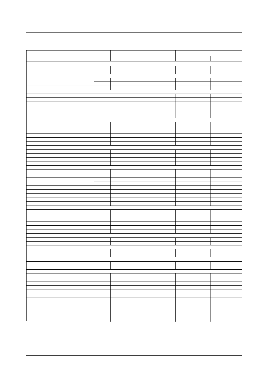
Parameter
Symbol
Conditions
Ratings
Unit
Maximum supply voltage
V
CC
max
4.5
V
Allowable power dissipation
Pd max
800
mW
Operating temperature
Topr
≠10 to +50
∞C
Storage temperature
Tstg
≠55 to +150
∞C
Specifications
Maximum Ratings
at Ta = 25∞C
Parameter
Symbol
Conditions
Ratings
Unit
Recommended supply voltage
V
CC
3.0
V
Operating voltage range
V
CC
op
1.8 to 3.6
V
Load resistance
(power block)
R
L
pwr
4
(preamplifier block)
R
L
pre
10
k
Operating Conditions
at Ta = 25∞C
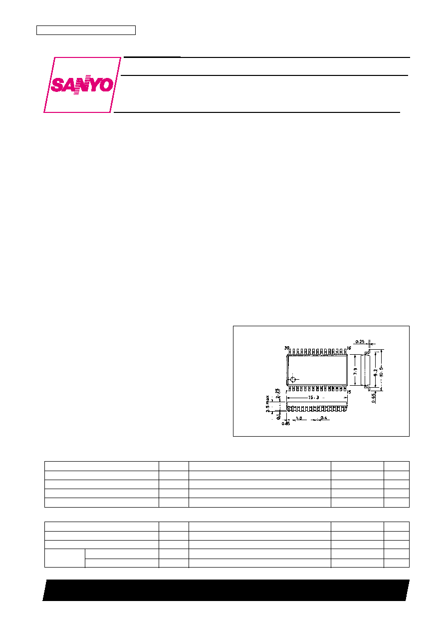
SANYO: MFP30SD
[LA4168M]
Package Dimensions
unit: mm
3073A-MFP30SD
No. 5660-2/6
LA4168M
Parameter
Symbol
Conditions
Ratings
Unit
min
typ
max
[PRE + POWER + GVN]
Standby current
I
STB
With pin 9 connected to V
CC
25
170
250
µA
through a 100-k
resistor
[PRE + POWER]
Quiescent current
I
CC-R
REC MODE, Vi = 0 V
6
12
18
mA
I
CC-P
PLAY MODE, Vi = 0 V, VOL MIN
12
18
25
mA
Voltage gain
VG
TP
PLAY MODE, V
O
= ≠5 dBm
71.5
74
76.5
dB
[EQ AMP]
Voltage gain (open loop)
VG
OP
C
NF
= 100 µF
80
85
dB
Voltage gain (closed loop)
VG
P
50
52
54
dB
Maximum output voltage
V
OP
max
THD = 1 %
0.5
0.75
V
Total harmonic distortion
THD
P
V
O
= 0.3 V
0.2
0.6
%
Equivalent input noise voltage
V
NIP
Rg = 2.2 k
, DIN audio
1.0
2.0
µV
Ripple rejection ratio
R
rp
Rg = 2.2 k
, f
R
= 1 kHz filter
45
60
dB
[MIC AMP] VOL MIN, ALC OFF
Voltage gain (closed loop)
VG
M
1
ALC OFF
43
45
47
dB
Maximum output voltage
V
OmaxM
THD = 1 %, R
L
= 10 k
0.5
0.75
V
Total harmonic distortion
THD
M
V
O
= 0.3 V
0.6
1.0
%
Equivalent input noise voltage
V
NIM
Rg = 3 k
, DIN audio
2.0
4.0
µV
Ripple rejection ratio
SVRR
Rg = 3 k
, f
R
= 1 kHz filter
40
53
dB
Input resistance
R
IM
24
32
40
k
[MIC + REC] VOL MIN
Voltage gain (closed loop)
VG
RT
ALC OFF
63.5
65.5
67.5
dB
Maximum output voltage
V
OmaxR
THD = 5 %
0.6
1.0
V
Output noise voltage
V
NORT
MIC Input, Rg = 3 k
, DIN audio
3.5
8.0
mV
Ripple rejection ratio
R
rRT
Rg = 3 k
, f
R
= 1 kHz , 1 kHz filter
20
32
dB
[POWER AMP]
Voltage gain (closed loop)
VG
BTL
BTL ON, V
O
= ≠10 dBm
21.5
24
26.5
dB
Voltage gain (closed loop)
VG
SIN
Single, V
O
= ≠10 dBm
20.5
23
25.5
dB
Output power
P
OBTL
THD = 10 %, BTL ON
200
350
mW
P
OSIN
THD = 10 %, Single
50
120
mW
Total harmonic distortion
THD
BTL
BTL ON, V
O
= 0.25 V
0.1
0.8
2
%
Output noise voltage
V
NOBTL
BTL ON, Rg = 0 k
20
50
µV
Ripple rejection ratio
R
rBTL
BTL ON, Rg = 0 k
, f
R
= 1 kHz , 1 kHz filter
50
70
dB
Output DC offset
V
DCOFF
BTL ON, Rg = 0 k
0
10
50
mV
Input resistance
R
INBTL
21
30
39
k
[ALC]
The input level width from the point the ALC
ALC width
ALC
W
circuit operates to the point the harmonic
40
67
dB
distortion reaches 5%
ALC harmonic distortion
ALC
THD
Vim = ≠40 dBm
1.0
2.0
%
ALC output
ALC V
O
Vim = ≠40 dBm
0.33
0.43
0.53
V
ALC start input
ALC V
IN
Vim = ≠40 dBm
≠79
≠74
≠69
dBm
[Voice Sensor (VOX)]
Operation start input voltage
V
OP min
VOLUME (10 k
) max
≠90
≠85
≠80
dBm
Input hysteresis
V
O HL
3
6
9
dB
[Auto-Stop]
Operation voltage
V
I ATS
The pin 9 voltage at the point the auto-stop
0.65
0.7
V
circuit operates
[LED]
LED drive current
I
LED
The input current when shorted
8
15
22
mA
through a 300-
resistor
[GVN]
Reference voltage
Vref
Im = 100 mA
1.1
1.25
1.4
V
Current division ratio
K
Im = 50 ≠ 100 mA
45
50
55
Residual voltage
Vsat
V
REF
= CONT, Im = 200mA
0.1
0.2
0.5
V
The CONT pin voltage in speed up mode
Vcont
0.35
0.41
0.47
V
Reference voltage/voltage characteristics
Vref
/
V
CC
V
CC
= 1.8 to 4.5 V, Im = 100 mA
0
0.2
0.6
%/V
Vref
Current division ratio/voltage characteristics
K
/
V
CC
V
CC
= 2.0 to 4.5 V, Im = 50 ≠ 100 mA
0
0.3
0.7
%/V
K
Reference voltage/current characteristics
Vref
/
Im Im = 50 ≠ 200 mA
0
0.002
0.03
%/mA
Vref
Current division ratio/current characteristics
K
/
Im
Im = 50 ≠ 100 mA to 150 ≠ 200 mA
≠0.07
0.03
+0.07
%/mA
Vref
Operating Characteristics
at Ta = 25∞C, V
CC
= 3.0 V, R
L
= 4
(power amplifier), R
L
= 10 k
(preamplifier),
f = 1 kHz, 0 dBm = 0.775 V

No. 5660-3/6
LA4168M
Block Diagram
Ambient temperature, Ta ≠ ∞C
Allowable power dissipation, Pd max ≠ mW
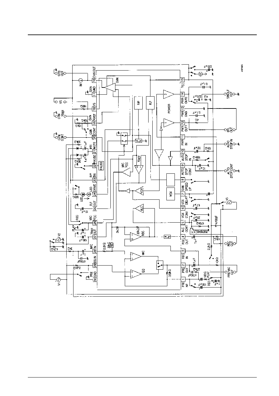
Test Circuit Diagram
No. 5660-4/6
LA4168M
Speed
No. 5660-5/6
LA4168M
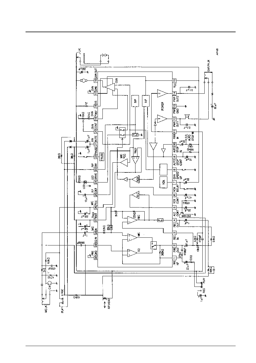
Sample Application Circuit
For the record/playback switch described above, during playback the power supply ripple may be output from the REC OUT pin (pin 4) and influence the
EQIN pin (pin 29). This problem can be minimized by adding a 5.6-k
resistor between pin 4 and pin 27.
Speed

No. 5660-6/6
LA4168M
This catalog provides information as of July, 1997. Specifications and information herein are subject to change
without notice.
s
No products described or contained herein are intended for use in surgical implants, life-support systems, aerospace
equipment, nuclear power control systems, vehicles, disaster/crime-prevention equipment and the like, the failure of
which may directly or indirectly cause injury, death or property loss.
s
Anyone purchasing any products described or contained herein for an above-mentioned use shall:
Accept full responsibility and indemnify and defend SANYO ELECTRIC CO., LTD., its affiliates, subsidiaries and
distributors and all their officers and employees, jointly and severally, against any and all claims and litigation and all
damages, cost and expenses associated with such use:
Not impose any responsibility for any fault or negligence which may be cited in any such claim or litigation on
SANYO ELECTRIC CO., LTD., its affiliates, subsidiaries and distributors or any of their officers and employees
jointly or severally.
s
Information (including circuit diagrams and circuit parameters) herein is for example only; it is not guaranteed for
volume production. SANYO believes information herein is accurate and reliable, but no guarantees are made or implied
regarding its use or any infringements of intellectual property rights or other rights of third parties.