 | –≠–ª–µ–∫—Ç—Ä–æ–Ω–Ω—ã–π –∫–æ–º–ø–æ–Ω–µ–Ω—Ç: LA4277 | –°–∫–∞—á–∞—Ç—å:  PDF PDF  ZIP ZIP |

Ordering number: ENN7095
SANYO Electric Co.,Ltd. Semiconductor Company
TOKYO OFFICE Tokyo Bldg., 1-10, 1 Chome, Ueno, Taito-ku, TOKYO, 110-8534 JAPAN
Any and all SANYO products described or contained herein do not have specifications that can handle
applications that require extremely high levels of reliability, such as life-support systems, aircraft's
control systems, or other applications whose failure can be reasonably expected to result in serious
physical and/or material damage. Consult with your SANYO representative nearest you before using
any SANYO products described or contained herein in such applications.
SANYO assumes no responsibility for equipment failures that result from using products at values that
exceed, even momentarily, rated values (such as maximum ratings, operating condition ranges, or other
parameters) listed in products specifications of any and all SANYO products described or contained
herein.
5 W 2-Channel Power Amplifier
LA4277
Monolithic Linear IC
41202RM (II) No. 7095-1/6
Package Dimensions
unit: mm
3248-SIP10HD
[LA4277]
SANYO: SIP10HD
Overview
The LA4277 is a 5 W 2-channel power amplifier intended
for televisions.
This IC has a series of pin compatible monaural and 2-
channel power amplifiers, thus allows the end product to
use a common circuit boad.
Features
∑ Television audio output.
∑ Pin compatible with the LA4266 (3 W)/LA4267 (5 W)/
4268 (10 W) and the LA4276 (3 W
◊ 2)/4278(10 W ◊ 2).
∑ Package: SIP-10HD (2.54 mm pitch, straight pins).
∑ Thermal protection circuit and overvoltage protection
circuit on chip.
∑ Output power: 5 W
◊ 2(V
CC
= 20 V/R
L
= 8
).
Specifications
Maximum Ratings at Ta = 25
∞C
Parameter
Symbol
Conditions
Ratings
Unit
Maximum supply voltage
V
CC
Rg = 0
25
V
Allowable power dissipation
Pd max
Infinite heat sink
15.0
W
Thermal resistance
j-c
3.0
∞C/W
Operating temperature
Topr
≠20 to +75
∞C
Storage temperature
Tstg
≠40 to +150
∞C
Operating Conditions at Ta = 25
∞C
Parameter
Symbol
Conditions
Ratings
Unit
Recommended supply voltage
V
CC
20
V
Load resistance
R
L
8
Operating supply voltage range
V
CC
op
Range does not exceed Pd
10 to 24
V
(11.8)
(10.0)
0.5
1.37
2.54
25.6
2.0
3.4
C0.7
15.4max
1.0 min
11.2
13.9
4.5
1
10
0.4
1.2
1.15
2.4
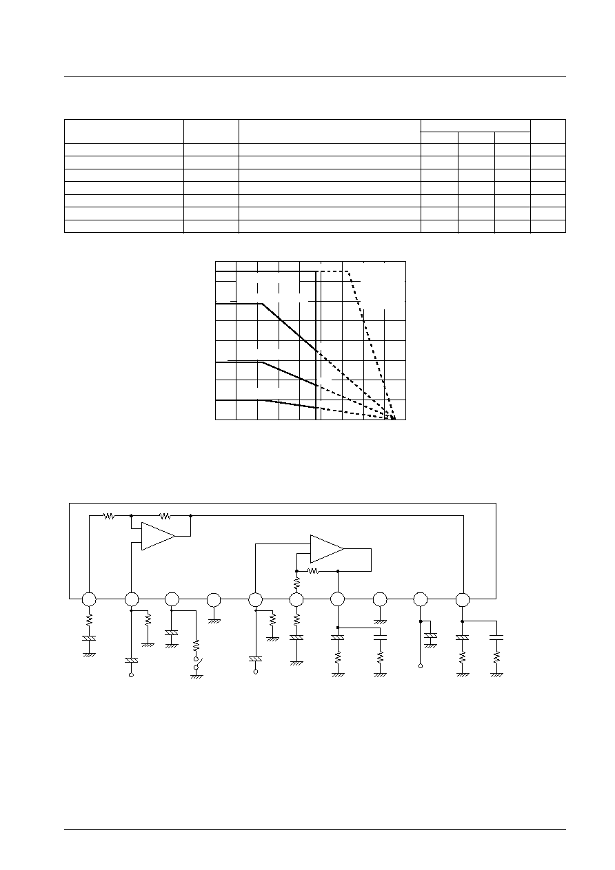
LA4277
No. 7095-2/6
Operating Characteristics at Ta = 25
∞C, V
CC
= 20 V, R
L
= 8
, f = 1 kHz, RNF = 150 , Rg = 600 , with specified
board, in specified circuit
Parameter
Symbol
Conditions
Ratings
min
typ
max
Unit
Quiescent current
I
CCO
Rg = 0
50
70
mA
Voltage gain
VG
V
O
= 0 dBm
38
40
42
dB
Total harmonic distortion
THD
P
O
= 0.5 W
0.1
0.8
%
Output noise voltage
V
NO
Rg = 10 k
, BPF = 20 Hz to 20 kHz
0.25
1.0
mV
Output power
P
O
THD = 10 %
4.0
5.0
W
Ripple rejection
SVRR
Rg = 0, f
r
= 100 Hz, Vr = 0.5 Vrms
35
45
dB
Crosstalk
CT
Rg = 10 k
, V
O
= 0 dBm
40
45
dB
0
Ambient temperature, Ta ≠
∞C
Pd max ≠ Ta
Allowable power dissipation, Pd max
≠
W
ILA00835
--20
16
12
14
6
8
10
4
2
20
0
40
60
80
100
120
140
160
15
15
11.7
5.8
2
7.02
3.48
1.2
Infinite heat sink
100
◊ 100 ◊ 1.5 mm
3
50
◊ 50 ◊ 1.5 mm
3
No heat sink
AI heat sink
Mounting
torque 39N∑cm
Flat washer
Silicone grease
applied
Pin Assignment and Equivalent Circuit Diagram
* For Muting, add a resistor between pin 3 and GND. 750
for the LA4266/67/68, 200 for the LA4276/77.
+
+
+
+
20 k
56
NF1
IN1
Filter
PRE GND
IN2
NF2
OUT2 Power GND
VCC
OUT1
C1
100
µ
F
R1
150
C4
4.7
µ
F
C5
100
µ
F
C6
1000
µ
F
C7
0.1
µ
F
R6
1.0
C8
1000
µ
F
RL
1
2
3
4
5
6
7
8
9
10
+
+
20 k
56
+
C2
4.7
µ
F
C3
100
µ
F
R2
100 k
R3
200
R4
100 k
R5
150
C9
1000
µ
F
C10
0.1
µ
F
RL
R7
1.0
LA4277
No. 7095-3/6
Description of External Parts
C1, C5: Feedback capacitors
Decreasing the capacitance value lowers the low frequency response. Increasing the capacitance value makes the
starting time later.
C2, C4: Input capacitors
C3: Ripple filter capacitor
Decreasing the capacitance value too far or eliminating it altogether causes ripple to occur. However, ripple is not
necessarily reduced if the capacitance value is increased. This capacitor also affects the starting time; decreasing the
capacitance value makes the starting time earlier.
C6, C9: Output capacitors
Decreasing the capacitance value causes insufficient power at low frequencies.
C7, C10: Oscillation blocking capacitors
Decreasing the capacitance value causes oscillation to occur easily. Use a mylar film capacitor that has good high
frequency response and temperature characteristics. The use of an electrolytic capacitor or a ceramic capacitor may
cause oscillation to occur at low temperatures.
C8: Power capacitor
Decreasing the capacitance value causes ripple to occur easily. Locating this capacitor at a distance from the IC or
removing this capacitor may cause oscillation to occur.
R1, R5: Feedback resistors
Refer to supplementary discussion "Voltage Gain."
R2, R4: Input bias resistors
These determine the bias (GND potential bias) and the input impedance of the input pins. If a variable resistor or
other device also serves this function, these resistors can be omitted.
R3: Muting resistor
Refer to supplementary discussion "External Muting."
R6, R7: Resistors connected in series with oscillation blocking capacitor
These prevent phase shift in conjunction with the oscillation blocking capacitor so that oscillation does not easily
occur. There is an optimal value for the resistor; increasing or decreasing the resistance causes oscillation to occur
easily.
External Muting
∑ Pull down the electric potential of the ripple filter pin (pin 3).
Muting becomes possible by inserting the discharge resistor R3 between pin 3
and GND. If the resistance value of R3 is too low, a popping noise is generated; if
the resistance value is too high, the muting effect is reduced. (A value of 200
is
recommended for R3.)
Voltage Gain
The voltage gain can be lowered by adding external resistors R1/R5 in
series to feedback capacitors C1/C5. When R1/R5 = 150
, the voltage
gain is 40 dB. However, it is important to note that because there is no
phase compensation pin, decreasing the voltage gain can extend the high
frequency characteristics, allowing oscillation to occur easily.
+
IN1
Filter
PRE GND
2
3
4
C3
R3
Mute SW
+
+
+
Rf 30 k
300
IN1/2
NF1/2
OUT1/2
C2/C4
RL
5
6
7
R1/R5
C1/C5
C6/C9
C7/C10
R2/R3
RNF
(1)
(2)
(10)
LA4277
No. 7095-4/6
Notes on Using the IC
∑ Maximum ratings
When this IC is used near its maximum ratings, it is possible that a slight fluctuation in the operating conditions could
cause the maximum ratings to be exceeded, damaging the IC. Therefore, allow for an adequate safety margin in
regards to supply voltage, etc., so that the IC is never used under conditions that exceed its maximum ratings.
∑ Short circuit between pins
Applying power to the IC while a short circuit exists between two pins can cause damage or deterioration in the IC.
Therefore, after mounting the IC on a board, make sure that there are no solder bridges, etc., causing a short circuit
between any of the pins before applying power to the IC.
∑ Using the IC in a radio
When using this IC in a radio, make sure that there is enough distance between the IC and the bar antenna.
∑ Printed circuit pattern
When designing the printed circuit pattern, keep power, output, and ground lines thick and short, and determine the
placement of the pattern and the components in such a way as to prevent the generation of an I/O feedback loop.
In addition, power supply capacitor C8 and oscillation blocking capacitor C7 and C10 should be placed as close as
possible to the IC pins in order to prevent oscillation.
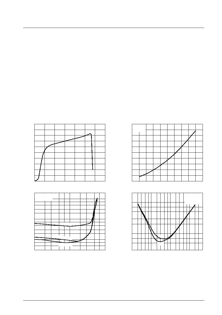
0
0
5
10
20
25
30
5
15
40
45
50
35
10
20
25
15
30
35
Supply voltage, VCC -- V
ICCO ≠ VCC
Quiescent current, I
CCO
--
mA
ILA00869
Rg = 0
Output power, PO -- W
THD ≠ PO
T
otal harmonic distortion,
THD -
-
%
ILA00871
Frequency, f -- Hz
THD ≠ f
T
otal harmonic distortion,
THD
--
%
ILA00872
6
0
2
4
6
8
10
8
16
20
12
24
14
18
10
22
26
Supply voltage, VCC -- V
PO
≠
VCC
Output power
, P
O
--
W
ILA00870
VCC = 20 V
RL = 8
0.1
1.0
2
3
5
7
10
2
3
5
7
10
7
5
3
2
7
5
3
2
2
1.0
7
5
3
0.1
10
100
2
3
5 7
2
3
5 7
2
3
5
2
3
5
7
1 k
10 k
7
5
3
2
7
5
3
2
1.0
0.1
f = 10 kHz
f = 100 Hz
f = 1 kHz
VCC = 20 V
RL = 8
PO = 0.5 W
CH1
CH2
RL = 8
f = 1 kHz
LA4277
No. 7095-5/6
0.1
1.0
2
3
5
7
3
5
7
7
5
3
2
7
5
3
2
3
2
10
1.0
0.1
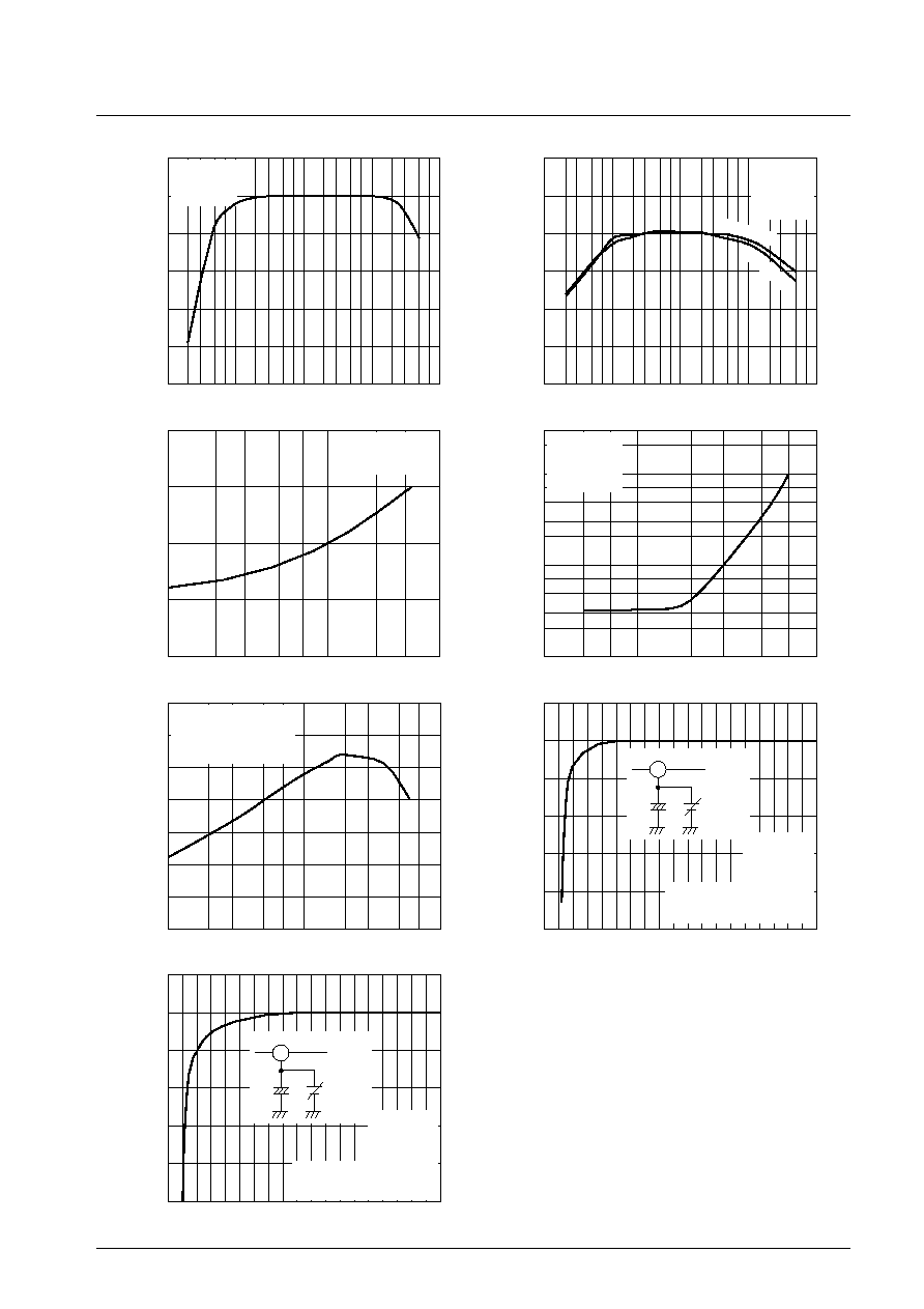
Frequency, f -- Hz
Response ≠ f
Response
--
dB
ILA00873
10
100
2 3
5 7
2 3
5 7
2 3
5 7
2 3
5 7
1 k
1 k
10 k
2
3
5
2
3
5
7
10 k
100 k
0
--1
--2
--3
--4
--5
1
Frequency, f -- Hz
CT ≠ f
Crosstalk, CT
--
dB
ILA00874
10
100
2 3
5 7
2 3
5 7
2 3
5 7
2 3
5 7
1 k
10 k
100 k
70
60
50
40
20
30
80
0
0.1
0.2
0.3
0.4
Input signal source resistance, Rg --
VNO ≠ Rg
Output noise voltage, VNO
--
mV
rms
ILA00875
Ripple voltage, Vr -- V
Vro ≠ Vr
Output ripple voltage, V
ro
--
mV
rms
ILA00876
VCC = 20 V
RL = 8
DIN Audio
VCC = 20 V
RL = 8
VO = 0
CH2CH1
CH1
CH2
VCC = 20 V
RL = 8
Rg = 10 k
VO = 0
VCC = 20 V
RL = 8
Rg = 0
fr = 100 Hz
Output power, PO -- W
Pd ≠ PO
Power dissipation, Pd
--
W
ILA00877
0.1
1.0
2
3
5
7
10
2
3
5
7
7
6
5
4
3
1
2
0
VCC = 20 V
RL = 8
f = 1 kHz
Pd = VCC ◊ ICC -- 2 ◊ PO
Pin 3 voltage, V3 -- V
ATT ≠ 3PINDC(1)
Muting attenuation,
A
T
T
--
dB
ILA00878
2
4
6
8
10
12
15
17
1
0
3
5
7
9
11
13 14
16
18 19
20
0
--20
--40
--80
--60
--100
Pin 3 voltage, V3 -- V
ATT ≠ 3PINDC(2)
Muting attenuation,
A
T
T
--
dB
ILA00879
2
4
6
8
10
12
15
17
1
0
3
5
7
9
11
13 14
16
18 19
20
0
--20
--40
--80
--60
--100
VCC = 20 V
RL = 8
VO = 2 Vrms
f = 1 kHz
BPF = 20 Hz to 20 kHz
Pin 3 voltage can be adjusted
by the external power supply
Filter
+
100 F
3
Filter
+
External
power
supply
100
F
3
VCC = 20 V
RL = 8
VO = 1 Vrms
f = 1 kHz
BPF = 20 Hz to 20 kHz
Pin 3 voltage can be adjusted
by the external power supply
External
power
supply