 | –≠–ª–µ–∫—Ç—Ä–æ–Ω–Ω—ã–π –∫–æ–º–ø–æ–Ω–µ–Ω—Ç: LA4450 | –°–∫–∞—á–∞—Ç—å:  PDF PDF  ZIP ZIP |
SANYO Electric Co.,Ltd. Semiconductor Bussiness Headquarters
TOKYO OFFICE Tokyo Bldg., 1-10, 1 Chome, Ueno, Taito-ku, TOKYO, 110-8534 JAPAN
Overview
The LA4450 is a single package two channel power IC
that supports an operating voltage of 26 V. It is partic-
ularly well suited for use as the bus or track power IC in
car stereo applications. Additionally, since the LA4450
can drive 4
loads, it can be used effectively in high-
power high-end products. Furthermore, since it supports a
high operating voltage and has low distortion, it is also
optimal for use in TV and home audio products.
Functions
∑ Standby switch (active on high (+5 V) input)
∑ On-chip impulse noise protection circuit
∑ On-chip thermal protection circuit
∑ On-chip overvoltage and surge protection circuits
Features
∑ Two channels in a single package
∑ P
O
= 12 W
◊
2 (V
CC
= 26.4 V, R
L
= 8
, THD = 10%)
∑ P
O
= 20 W
◊
2 (V
CC
= 26.4 V, R
L
= 4
, THD = 10%)
∑ Can drive 4
speakers
∑ Built-in standby switch
∑ Minimizes impulse noises
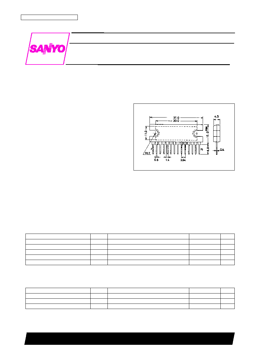
Package Dimensions
unit: mm
3023A-SIP14H
Specifications
Maximum Ratings
at Ta = 25∞C
Note:
*
Set V
CC
and R
L
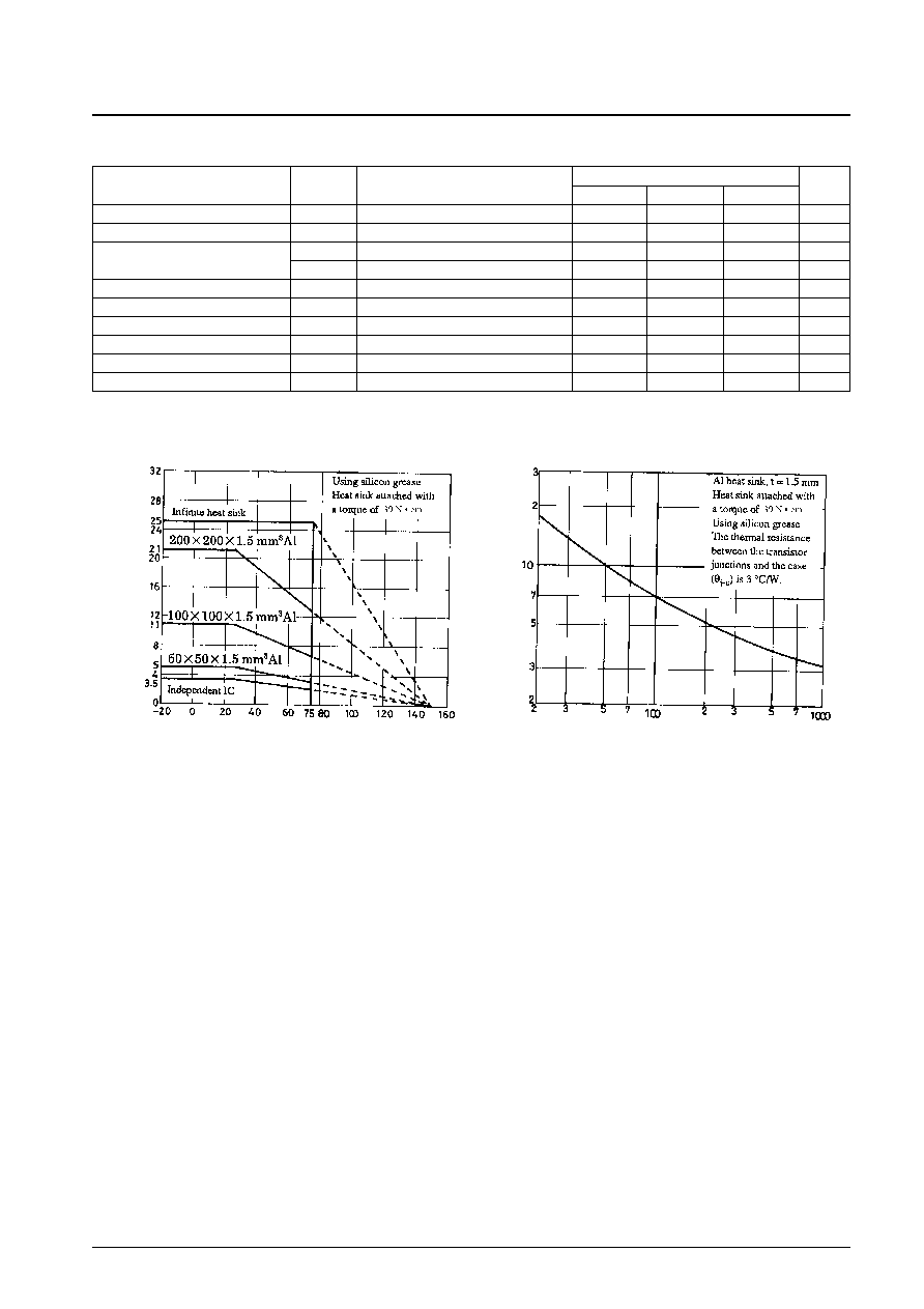
within ranges that do not cause Pd max to exceed 25 W.
(When V
CC
is 37 V, R
L
should be 6
or larger and when V
CC
is 35 V, R
L
should be 4
or larger.)
Operating Conditions
at Ta = 25∞C
Parameter
Symbol
Conditions
Ratings
Unit
Maximum supply voltage
V
CC
max
Rg = 0 (no signal)
37
V
Maximum output current
I
O
peak
4
A
Allowable power dissipation
Pd max
*
Infinite heat sink
25
W
Operating temperature
Topr
≠35 to +80
∞C
Storage temperature
Tstg
≠40 to +150
∞C
Parameter
Symbol
Conditions
Ratings
Unit
Recommended supply voltage
V
CC
26.4
V
Recommended load resistance
R
L
8
Operating supply voltage range
V
CC
op
10 to 30
V
Monolithic Linear IC
Ordering number : EN4090C
LA4450
Two Channel Power IC for Bus or Track
Use in TV and Home Audio Applications
43098HA (OT)/10794TS B8-0618/1102 No. 4090-1/7
SANYO Electric Co.,Ltd. Semiconductor Bussiness Headquarters
TOKYO OFFICE Tokyo Bldg., 1-10, 1 Chome, Ueno, Taito-ku, TOKYO, 110-8534 JAPAN
SANYO: SIP-14H
[LA4450]
Operating Characteristics
at Ta = 25∞C, V
CC
= 26.4 V, R
L
= 8
, f = 1 kHz, Rg = 600
No. 4090-2/7
LA4450
Parameter
Symbol
Conditions
Ratings
Unit
min
typ
max
Standby current
Ist
Standby switch off
1
30
µA
Quiescent current
I
CCO
Rg = 0
50
80
140
mA
Output power
P
O1
THD = 10%
10
12
W
P
O2
THD = 10%, R
L
= 4
20
W
Voltage gain
VG
V
O
= 0 dBm
49
51
53
dB
Total harmonic distortion
THD
P
O
= 1 W
0.07
0.4
%
Output noise voltage
V
NO
Rg = 0, BPF-BW = 20 Hz to 20 kHz
0.4
1.0
mV
Ripple exclusion ratio
SVRR
Rg = 0, f
R
= 100 Hz, V
R
= 0 dBm
45
55
dB
Channel separation
CHsep
V
O
= 0 dBm, Rg = 10 k
45
55
dB
Standby control voltage
Vst
With a 10 k
resistor connected at pin 12
2.5
V
CC
V
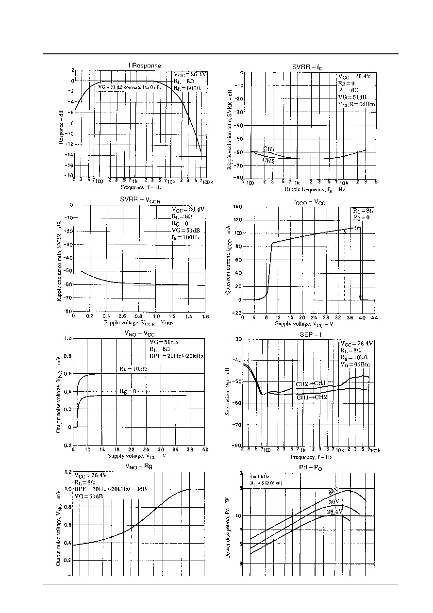
Pd max ≠ Ta
Allowable power dissipation, Pdmax ≠ W
Ambient temperature, Ta ≠ ∞C
f
≠ S
f
Heat sink thermal resistance,
f
≠
∞
C/W
Heat sink surface area, S
f
≠ cm
2
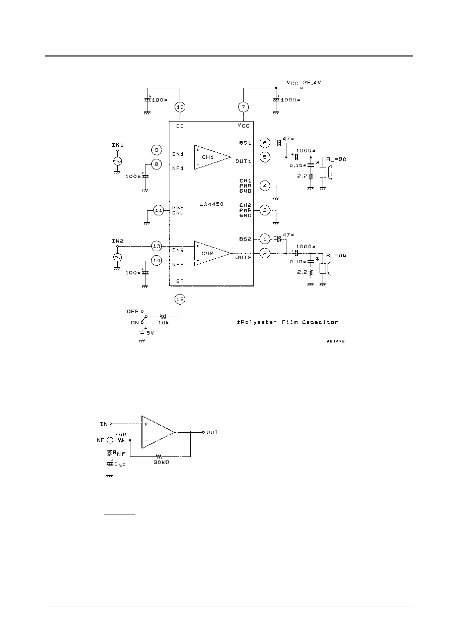
Test Circuit
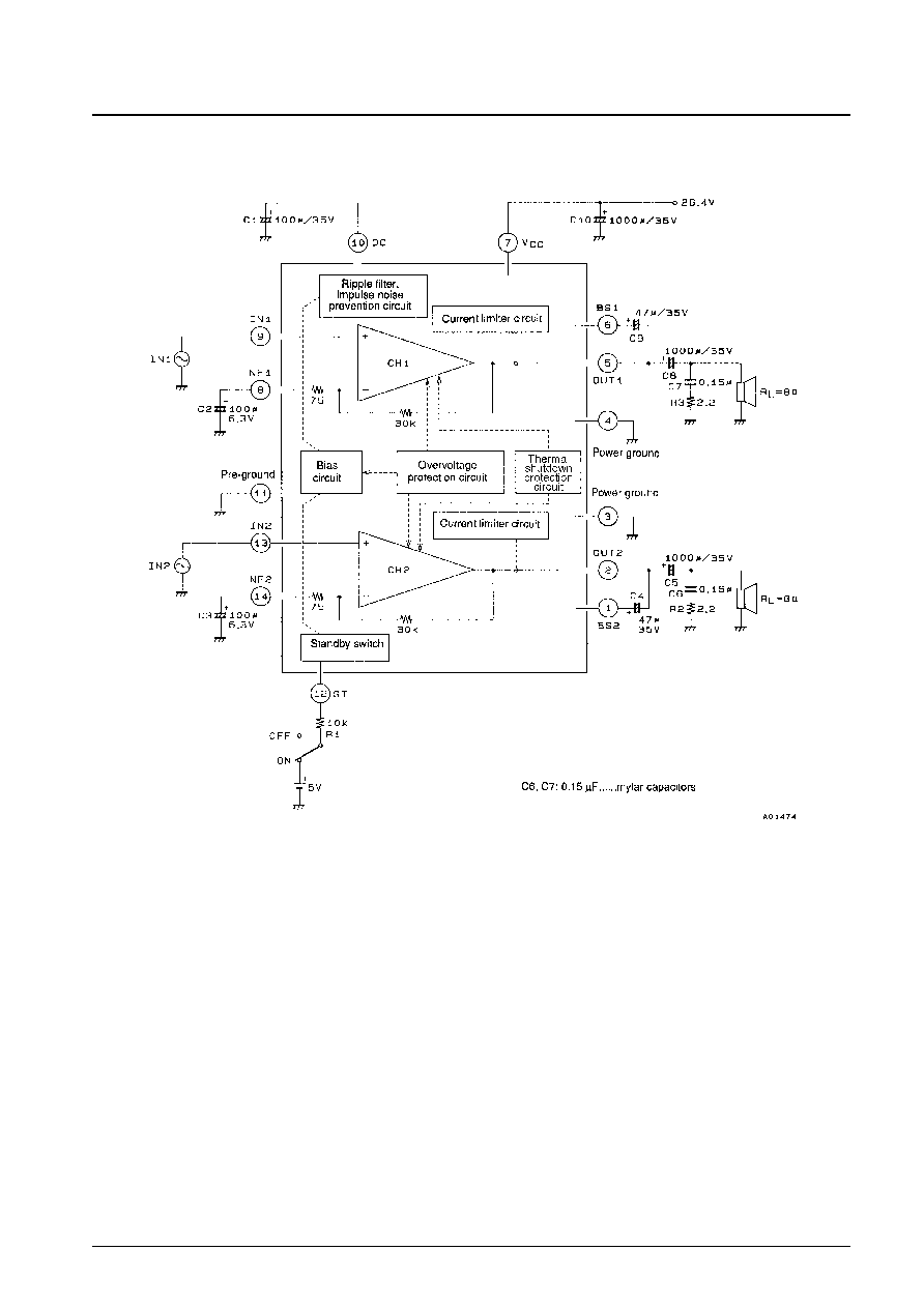
1. Features and Usage Notes
∑ Pin 12 is the standby pin. The IC operates when a voltage of 2 V or higher is applied through the external resistor
R1. Note that the maximum influx current to pin 12 is 500 µA.
∑ Changing the voltage gain
The voltage gain VG can be lowered by connecting an external resistor in series between the NF pin (pins 8 and
14) and C
NF
.
VG = 20 log
However, since the IC may oscillate if VG is 30 dB or lower, use a VG of 36 dB or higher.
∑ The LA4450 includes a thermal protection circuit to prevent damage to or destruction of the IC due to abnormal
overheating. As a result, the output may be attenuated or cut off if the application heat sinking is inadequate.
∑ The LA4450 includes an overvoltage protection circuit to protect the IC against power supply surges and abnormal
voltages. This circuit has hysteresis characteristics: it operates at between 39 and 40 V, and recovers at around 34 V.
∑ Although the LA4450 includes a current limiter circuit to prevent damage due to abnormal currents, care must still
be exercised to prevent load shorts and other excessive current conditions.
30 k
75 + R
Nf'
No. 4090-3/7
LA4450
Unit (resistance :
, capacitance : F)
Sample Application Circuit
No. 4090-4/7
LA4450
Unit (resistance :
, capacitance : F)
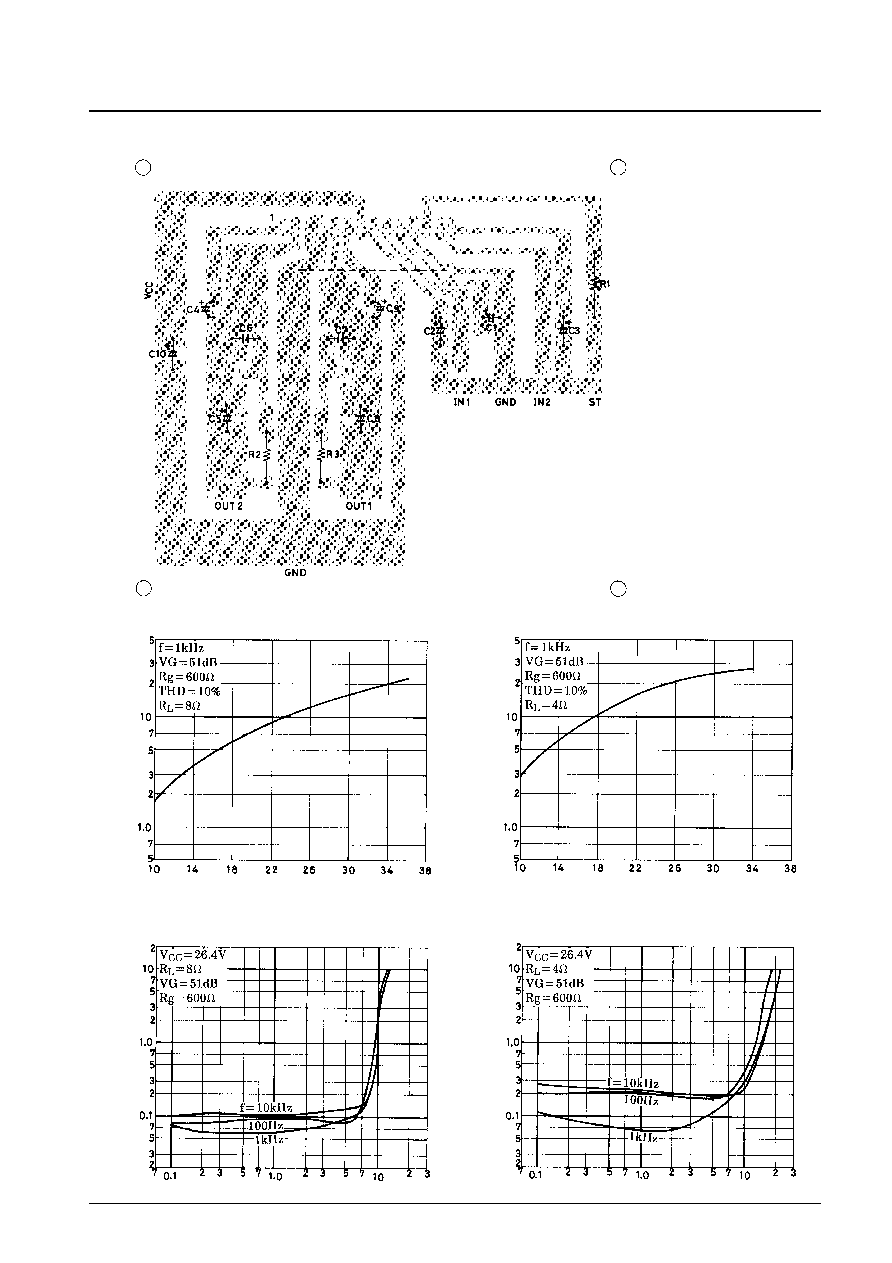
Printed Circuit Board Pattern Example
No. 4090-5/7
LA4450
P
O
≠ V
CC
Output power, P
O
≠ W
Supply voltage, V
CC
≠ V
P
O
≠ V
CC
Output power, P
O
≠ W
Supply voltage, V
CC
≠ V
THD ≠ P
O
Total harmonic distortion, THD ≠ %
Output power, P
O
≠ W
THD ≠ P
O
Total harmonic distortion, THD ≠ %
Output power, P
O
≠ W
C opper foiled side
90
◊
100 mm
2
No. 4090-6/7
LA4450
No. 4090-7/7
LA4450
This catalog provides information as of April, 1998. Specifications and information herein are subject to change
without notice.
s
No products described or contained herein are intended for use in surgical implants, life-support systems, aerospace
equipment, nuclear power control systems, vehicles, disaster/crime-prevention equipment and the like, the failure of
which may directly or indirectly cause injury, death or property loss.
s
Anyone purchasing any products described or contained herein for an above-mentioned use shall:
Accept full responsibility and indemnify and defend SANYO ELECTRIC CO., LTD., its affiliates, subsidiaries and
distributors and all their officers and employees, jointly and severally, against any and all claims and litigation and all
damages, cost and expenses associated with such use:
Not impose any responsibility for any fault or negligence which may be cited in any such claim or litigation on
SANYO ELECTRIC CO., LTD., its affiliates, subsidiaries and distributors or any of their officers and employees
jointly or severally.
s
Information (including circuit diagrams and circuit parameters) herein is for example only; it is not guaranteed for
volume production. SANYO believes information herein is accurate and reliable, but no guarantees are made or implied
regarding its use or any infringements of intellectual property rights or other rights of third parties.