 | –≠–ª–µ–∫—Ç—Ä–æ–Ω–Ω—ã–π –∫–æ–º–ø–æ–Ω–µ–Ω—Ç: LA4592W | –°–∫–∞—á–∞—Ç—å:  PDF PDF  ZIP ZIP |
Overview
The LA4592W is a single-chip 1.5-V headphone stereo
system IC. The LA4592W adds a variety of functions,
including a switch amplifier (for end product audio quality
switches, the metal tape switch, and other switches) and an
AMSS (Automatic Music Search System) function that
supports blank skipping, to the earlier LA4590W.
Furthermore, the LA4592W provides even lower no-signal
time power levels for lower end-product power
dissipation. In combination with the LA3235W 1.5-V
record preamplifier IC, the LA4592W can be used to
implement a record/playback cassette system with just two
ICs.
Functions
∑ Stereo preamplifier: supports auto reverse and includes a
muting function.
∑ Stereo power amplifier: Includes OCL and muting
functions.
∑ Ripple filter
∑ Low boost function (BTL operation in the low-
frequency region)
∑ Inter-track detection function (Supports AMSS and
blank skipping)
∑ Two switching amplifiers
∑ Power switch (standby function)
Features
∑ Virtual ground impedance is reduced by built-in V
REF
amplifier
∑ No capacitor required for ripple filter oscillation
prevention.
∑ Provides ample output power at low frequencies.
(P
O
= 24 mW, V
CC
= 1.2 V, f = 150 Hz)
∑ High-frequency cutoff capacitors built into the
preamplifier and power amplifier inputs to minimize
buzzing.
Monolithic Linear IC
Ordering number : EN5662
73097HA (OT) No. 5662-1/5
SANYO: SQFP48
[LA4592W]
SANYO Electric Co.,Ltd. Semiconductor Bussiness Headquarters
TOKYO OFFICE Tokyo Bldg., 1-10, 1 Chome, Ueno, Taito-ku, TOKYO, 110 JAPAN
1.5-V Preamplifier + Power Amplifier
for Headphone Stereo Products
LA4592W
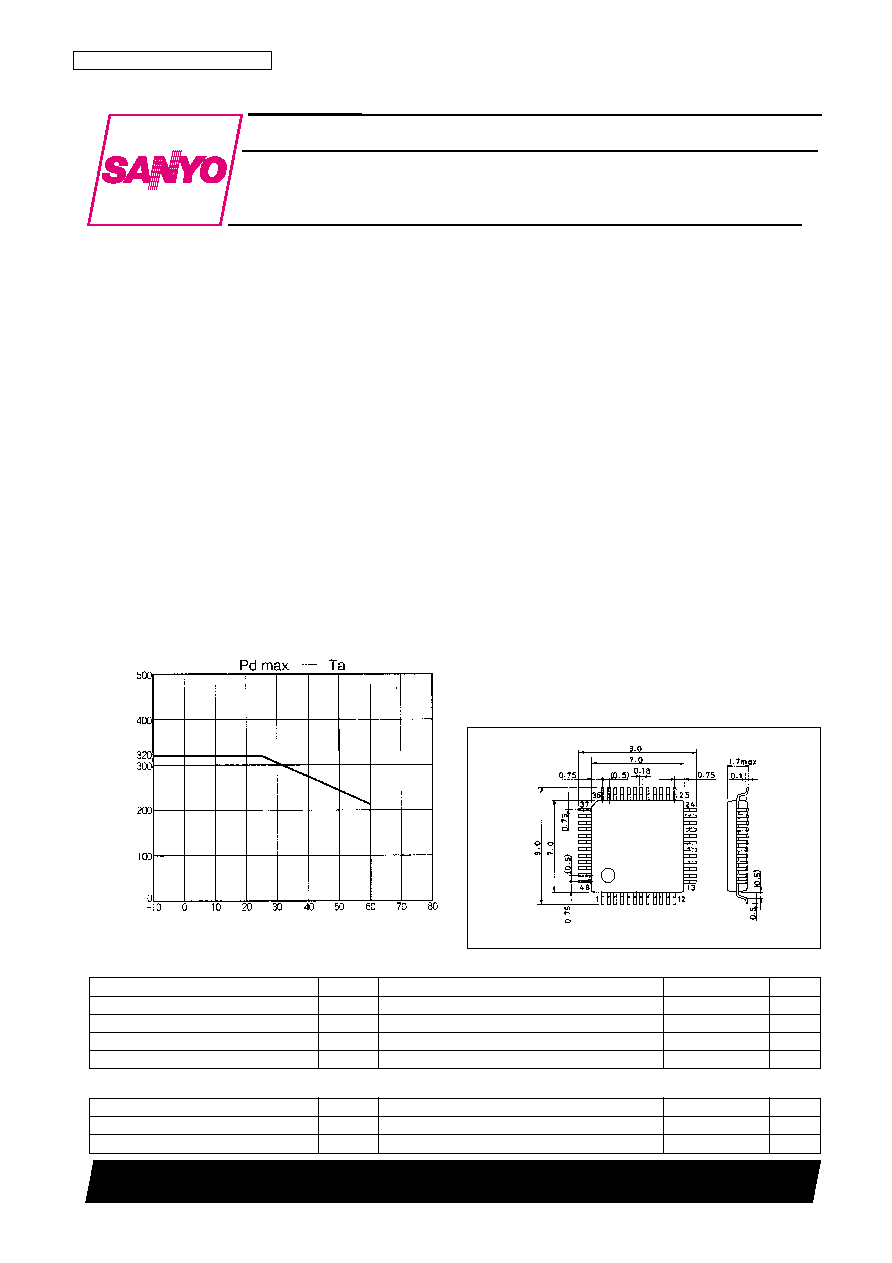
Package Dimensions
unit: mm
3163A-SQFP48
Parameter
Symbol
Conditions
Ratings
Unit
Maximum supply voltage
V
CC
max
3.0
V
Allowable power dissipation
Pd max
320
mW
Operating temperature
Topr
≠10 to +60
∞C
Storage temperature
Tstg
≠40 to +125
∞C
Specifications
Maximum Ratings
at Ta = 25∞C
Parameter
Symbol
Conditions
Ratings
Unit
Recommended supply voltage
V
CC
1.5
V
Operating supply voltage range
V
CC
op
0.95 to 2.2
V
Allowable Operating Ranges
at Ta = 25∞C
Ambient temperature, Ta ≠ ∞C
Allowable power dissipation, Pd max ≠ W

No. 5662-2/5
LA4592W
Parameter
Symbol
Conditions
Ratings
Unit
min
typ
max
[PRE + PWR]
Quiescent current
I
CCO
1
Rg = 2.2 k
, R
V
= 0
8.5
11
16
mA
I
CCO
2
With the power switch off
0.1
5
µA
Voltage gain (closed loop)
VG
T
V
O
= ≠20 dBm, R
V
= 10 k
54
57
60
dB
[PRE AMP]
Voltage gain (open loop)
VG
0
V
O
= ≠20dBm
60
68
dB
Voltage gain (closed loop)
VG
1
V
O
= ≠20dBm
34
35.3
37
dB
Maximum output voltage
V
O
max1
THD = 1 %
100
210
mV
Total harmonic distortion
THD1
VG = 35.3 dB/NAB, V
O
= 100 mV
0.08
0.5
%
Equivalent input noise voltage
V
N
1
Rg = 2.2 k
, BPF = 20 Hz to 20 kHz
1.3
3.0
µV
Interchannel crosstalk
CT1
Rg = 2.2 k
, TUNE 1 kHz, V
O
= ≠20 dBm
45
56
dB
F/R crosstalk
CT2
Rg = 2.2 k
, TUNE 1 kHz, V
O
= ≠20 dBm
65
78
dB
Ripple rejection ratio
R
r
1
Rg = 2.2 k
, Vr = ≠30 dBm,
45
52
dB
fr = 100 Hz, TUNE 100 Hz
Muting output voltage
V
M
1
V
IN
= ≠40 dBm, TUNR 1 kHz,
≠90
dBm
With the muting function on
[Low Boost + Power Amplifier]
VG
3
V
O
= ≠20 dBm
20.5
23
25.5
dB
Voltage gain (closed loop)
VG
4
V
O
= ≠20 dBm, L.B = ON
20.5
23
25.5
dB
VG
5
V
O
= ≠20 dBm, L.B = ON, f = 10 kHz
24.5
27.5
30.5
dB
VG
6
V
O
= ≠20 dBm, L.B = ON, f = 100 Hz
28
32
36
dB
Output voltage
P
O
1
THD = 10 %
5
9
mW
P
O
2
THD = 10 %, f = 100 Hz, L.B = ON
13
19
mW
Total harmonic distortion
THD2
P
O
= 1 mW
0.3
1.5
%
Interchannel crosstalk
CT3
V
O
= ≠20 dBm, R
V
= 0
38
43
dB
Output noise voltage
V
NO
R
V
= 0
, BPF = 20 Hz to 20 kHz
20
33
µV
Ripple rejection ratio
R
r
2
R
V
= 0
, Vr = ≠30 dBm,
50
74
dB
fr = 100 Hz, TUNE 100 Hz
Muting output voltage
V
M
2
V
IN
= ≠30 dBm, TUNE 1 kHz,
≠90
dBm
With the muting function on
Input resistance
Ri
8
10
12
k
Voltage gain difference
VG3
0
1.5
dB
[Ripple Filter]
Ripple rejection ratio
R
r
3
fr = 100 Hz, Vr = ≠30 dBm, V
CC
= 1.0 V,
33
39
dB
I
RF
= 25 mA, using a rank 6 2SB1295
Output voltage
V
RF
V
CC
= 1.0 V, I
RF
= 25 mA
0.89
0.94
V
[AMSS]
The preamplifier output voltage
Operating output voltage
V
OAMSS
1
when the AMSS V
O
= 0.6 V p-o
3.33
4.7
6.64
mV
With the PWR muting on. (AMSS)
The preamplifier output voltage
Operating output voltage
V
OAMSS
2
when the AMSS V
O
= 0.6 V p-o
479
675
953
µV
With the PWR muting off. (BLANK SKIP)
The preamplifier output voltage
Operating output voltage
V
OAMSS
3
when the AMSS V
O
= 0.6 V p-o
2.62
3.7
5.23
mV
With pin 34 shorted through a 270-
resistor.
With the PWR muting on.
The preamplifier output voltage
Operating output voltage
V
OAMSS
4
when the AMSS V
O
= 0.6 V p-o
375
530
749
µV
With pin 34 shorted through a 270-
resistor.
With the PWR muting on.
[SW AMP]
Voltage gain (closed loop)
VG
7
V
O
= ≠25 dBm
≠1.2
≠0.7
≠0.2
dB
Maximum output voltage
V
O
max2
THD = 1 %
25
60
mV
Ripple rejection ratio
R
r
4
With the input pins open, Vr = ≠30 dBm,
50
75
dB
fr = 100 Hz, TUNE 100 Hz
Output voltage when off
V
M
3
V
IN
= ≠20 dBm, TUNE 1 kHz, SW OFF
≠90
dBm
Operating Characteristics
at Ta = 25∞C, V
CC
= 1.2 V, f = 1 kHz, 0.775 V = 0 dB, R
L
= 10 k
(preamplifier)
RL = 16
(power amplifier)

No. 5662-3/5
LA4592W
Parameter
Symbol
Conditions
Ratings
Unit
min
typ
max
AMSS
Ta
≠10
25
50
∞C
The preamplifier output voltage
V
OAMSS1
when the AMSS V
O
= 0.6 V p-o
3.9
4.7
5.4
mV
Operating output voltage
With the PWR muting on. (AMSS)
The preamplifier output voltage
V
OAMSS2
when the AMSS V
O
= 0.6 V p-o
605
675
735
µV
AMSS Temperature Characteristics (Values for reference only)
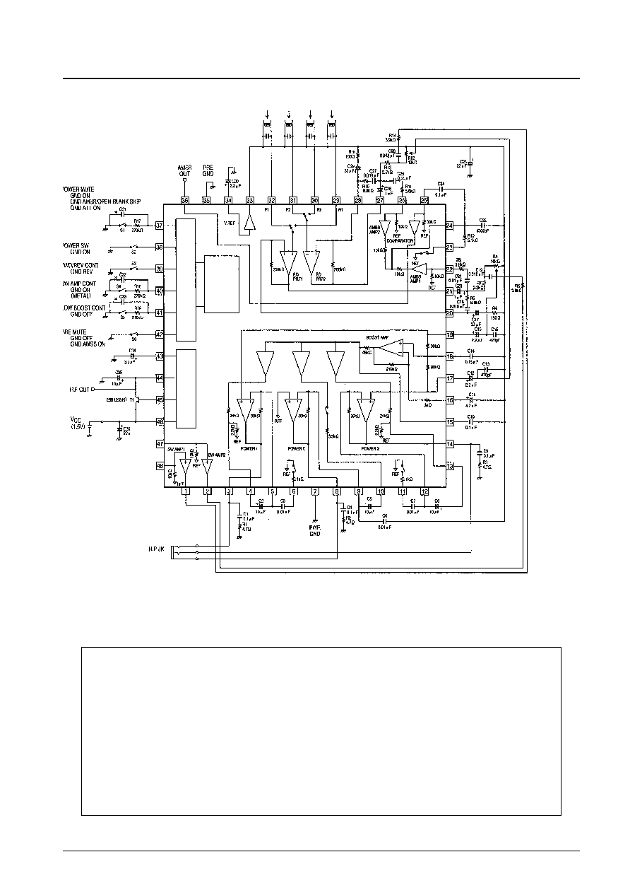
Block Diagram
System control
Bias
Ripple filter

Test Circuit Diagram
No. 5662-4/5
LA4592W
System control
Bias
Ripple filter
No. 5662-5/5
LA4592W
This catalog provides information as of July, 1997. Specifications and information herein are subject to change
without notice.
s
No products described or contained herein are intended for use in surgical implants, life-support systems, aerospace
equipment, nuclear power control systems, vehicles, disaster/crime-prevention equipment and the like, the failure of
which may directly or indirectly cause injury, death or property loss.
s
Anyone purchasing any products described or contained herein for an above-mentioned use shall:
Accept full responsibility and indemnify and defend SANYO ELECTRIC CO., LTD., its affiliates, subsidiaries and
distributors and all their officers and employees, jointly and severally, against any and all claims and litigation and all
damages, cost and expenses associated with such use:
Not impose any responsibility for any fault or negligence which may be cited in any such claim or litigation on
SANYO ELECTRIC CO., LTD., its affiliates, subsidiaries and distributors or any of their officers and employees
jointly or severally.
s
Information (including circuit diagrams and circuit parameters) herein is for example only; it is not guaranteed for
volume production. SANYO believes information herein is accurate and reliable, but no guarantees are made or implied
regarding its use or any infringements of intellectual property rights or other rights of third parties.
Sample Application Circuit
*
: Adjust the values of the capacitors marked with an asterisk to match the timing required by the end product.
System control
Bias
Ripple filter