 | –≠–ª–µ–∫—Ç—Ä–æ–Ω–Ω—ã–π –∫–æ–º–ø–æ–Ω–µ–Ω—Ç: LA4632 | –°–∫–∞—á–∞—Ç—å:  PDF PDF  ZIP ZIP |
Overview
The LA4632 is a pin compatible version of the LA4631 (5 W
◊
two channel single ended type) BTL power amplifier
IC. The LA4632's pin compatibility makes it possible to share a common printed circuit board among a series of end
products differentiated by power rank. Note that the LA4631 has a pin 13, and that it is necessary to provide a hole for
this pin if the same printed circuit board is to be shared. Also, some of the external components used differ. The
LA4632 provides a full complement of built-in protection circuits, including protection against shorting to the power
supply, shorting to ground, load shorting, and excessive temperatures.
Functions and Applications
∑ Two-channel BTL power amplifier for audio applications
Absolute Maximum Ratings
at Ta = 25∞C
Operating Characteristics
at Ta = 25∞C
Caution: V
CC
, R
L
, and the output level must be set for the size of the heat sink used so that the Pd max range is not exceeded.
*
1. When both channels are operating such that I
O
peak = 1.0 A per channel is exceeded.
If the IC is operated such that I
O
peak = 1.0 A per channel is not exceeded, the IC can be used in the range 5.5 to 20 V (in the ranges where Pd max is
not exceeded) with a load of R
L
= 4 to 8
.
Parameter
Symbol
Conditions
Rated value
Unit
Recommended supply voltage
V
CC
13
V
Recommended load resistance range
R
L
op
4 to 8
Allowable operating supply voltage range
*
1
V
CC
op
When RL = 8
5.5 to 20
V
When RL = 6
5.5 to 17
V
When RL = 4
5.5 to 13
V
Parameter
Symbol
Conditions
Rated value
Unit
Maximum supply voltage
V
CC
max
With no input signal
24
V
Maximum output current
I
O
peak
Per channel
2.5
A
Allowable power dissipation
Pd max
With an infinitely large heat sink
25
W
Maximum junction temperature
Tj max
150
∞C
Operating temperature
Topr
≠20 to +75
∞C
Storage temperature
Tstg
≠40 to +150
∞C
SANYO Electric Co.,Ltd. Semiconductor Company
TOKYO OFFICE Tokyo Bldg., 1-10, 1 Chome, Ueno, Taito-ku, TOKYO, 110-8534 JAPAN
Ordering number : ENN8178
33105TN (OT) No.8178-1/8
SANYO Semiconductors
DATA SHEET
LA4632
Monolithic Linear IC
10 W Two-Channel BTL AF Power
Amplifier for Audio Applications
Any and all SANYO products described or contained herein do not have specifications that can handle
applications that require extremely high levels of reliability, such as life-support systems, aircraft's
control systems, or other applications whose failure can be reasonably expected to result in serious
physical and/or material damage. Consult with your SANYO representative nearest you before using
any SANYO products described or contained herein in such applications.
SANYO assumes no responsibility for equipment failures that result from using products at values that
exceed, even momentarily, rated values (such as maximum ratings, operating condition ranges, or other
parameters) listed in products specifications of any and all SANYO products described or contained
herein.

Parameter
Symbol
Conditions
Ratings
Unit
min
typ
max
Quiescent current drain
I
CCO
Rg = 0, no signal
40
70
150
mA
Standby current
Ist
0
10
µA
Voltage gain
VG
V
O
= 0 dBm
33
35
37
dB
Total harmonic distortion
THD
P
O
= 1 W
0.06
0.2
%
Output power
P
O
THD = 10 %
8.5
10
W
Output offset voltage
V
N
offset
Rg = 0
≠300
+300
mV
Output noise voltage
V
NO
Rg = 0, BPF = 20 Hz to 20 kHz
0.14
0.3
mVrms
Supply voltage rejection ratio
SVRR
Rg = 0, f
R
= 100Hz, VR = 0 dBm
50
60
dB
Channel separation
CH sep
Rg = 10 k
, V
O
= 0 dBm
50
60
dB
Input resistance
Ri
14
20
26
k
Standby pin applied voltage
VST
The pin 5 voltage such that the amplifier is on
2.5
10
V
Mute pin applied voltage
VM
The pin 6 voltage such that muting is applied
1.7
3
V
Muting attenuation
ATTM
V
O
= 1 Vrms, BPF = 20 Hz to 20 kHz
80
90
dB
No.8178-2/8
LA4632
SANYO : SIP12H
26.8
(20.0)
(R1.7)
(8.4)
12
1
(11.8)
0.5
2.0
4.0
0.4
2.0
7.0
(2.4)
1.0
13.2max
6.0
1.0min
0
Pd max -- Ta
ILA06994
--20
30
20
25
5
10
15
20
0
40
60
80
100
120
140
160
f=3
∞
C/W
f=4
∞
C/W
f=7
∞
C/W
f=10
∞
C/W
No radiator fin
jc=2
∞
C/W
20.8
13.9
10.4
3.1
With an infinitely
large heat sink
Aluminum heat sink, t = 1.5 mm
Tightening torque: 39 N cm
With silicone grease applied
Allo
w
a
b
le po
w
er dissipation, Pd max -
W
Ambient temperature, Ta -
∞
C
Operating Characteristics
at Ta = 25 ∞C, V
CC
= 13 V, R
L
= 6
, f = 1kHz, Rg = 600
Package Dimensions
unit : mm
3049B
No.8178-3/8
LA4632
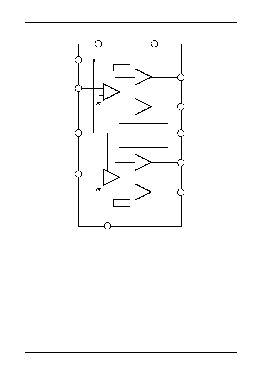
Block Diagram
5
7
12
11
10
8
9
1
4
3
2
6
+
≠
CH1
Input amplifier
Input amplifier
Output amplifier
Protection circuits
Protection against shorting to
the power supply, shorting to
ground, load shorting, and
excessive temperatures
Ripple filter/startup timer
+OUT1
≠OUT1
+
≠
CH2
Output amplifier
+OUT2
≠OUT2
SIGNAL
MUTE
IN1
PRE
GND
PWR
GND
IN2
STAND BY
VCC
No.8178-4/8
LA4632
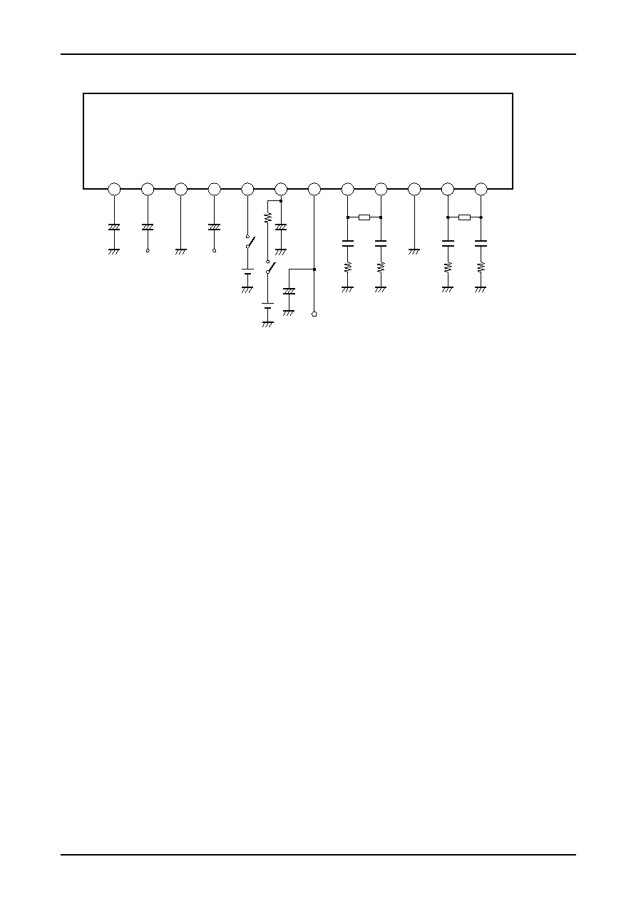
Application Circuit Example/Test Circuit Diagram
+
RF
+
IN1
+
C2 4.7
µ
F 16V
C4 10
µ
F 10V
C1 4.7
µ
F 16V
C3 47
µ
F 25V
IN2
+
C5 1000
µ
F 25V
MUTE
PWR
GND
+OUT2
--OUT2
--OUT1
STBY
VCC
VCC
PRE
GND
STBY 5V
+
+OUT1
LA4632
R1 15k
Mute 5V
1
2
3
4
5
6
7
10
11
12
RL
C8 0.1
µ
F
C9 0.1
µ
F
C6 0.1
µ
F
C7 0.1
µ
F
R5 2.2
R4 2.2
R3 2.2
R2 2.2
RL
8
9
Top view
∑ Caution
Although the LA4632 is basically pin compatible with the LA4631, there are certain differences in the external
components and the way the devices are used.
External Components and Usage Notes
C1, C2: These are input coupling capacitors; we recommend a value of 4.7 µF or lower. A zero bias type circuit is
used for the LA4632 input circuits, and the input pin potential is close to zero volts. Therefore the polarity
must be considered in conjunction with the DC potential of the circuit connected to the LA4632 front end.
If there is a large potential difference between the plus and minus sides of the input capacitors, the
stabilization time when power is first applied can be reduced by reducing the value of the input
capacitors, as long as that reduction does not compromise the low-band characteristics.
C3:
This capacitor is used both as a ripple filter and to set the amplifier's startup time. A value of 47 µF is
recommended. With this value, the startup time (the time from the point power is first applied until the
point an output is generated) will be about 0.6 to 0.7 seconds. (See note 1.)
C4, R1: This RC circuit is used for mute smoothing. C4 is required even if the muting function is not used. (See
note 2.)
C5:
Power supply capacitor
C6 to C9, R2 to R5: These components form oscillation prevention RC circuits. We recommend using polyester
film capacitors (Mylar capacitors) with excellent thermal characteristics for C6 through C9. (R2 to R5 are
2.2
1/4 W resistors.)
*1. Startup time
The LA4632 features a built-in startup circuit that can be adjusted somewhat by changing the value of the capacitor
connected to pin 1. (With the recommended value of 47 µF, the time is about 0.6 to 0.7 seconds (a time that changes
somewhat with V
CC
). That time can be extended to about 0.8 to 0.9 seconds by inserting a capacitor with a value of
10 µF in parallel.) Since using a capacitor with a value smaller than the recommended value may reduce the SVRR
between ground and the output, we cannot recommend using a smaller value.
*2. Signal muting function
The signal muting function is turned on by connecting the recommended RC circuit (10 µF, 15 k
) to pin 6 and
applying a voltage of +5 V to the mute pin. This circuit implements a muting function with extremely low impulse
noise.
This RC circuit is used to smooth the attack and recovery times, and since the 10 µF capacitor also has the function
of smoothing after the startup time, it is required even if the signal muting function is not used.
No.8178-5/8
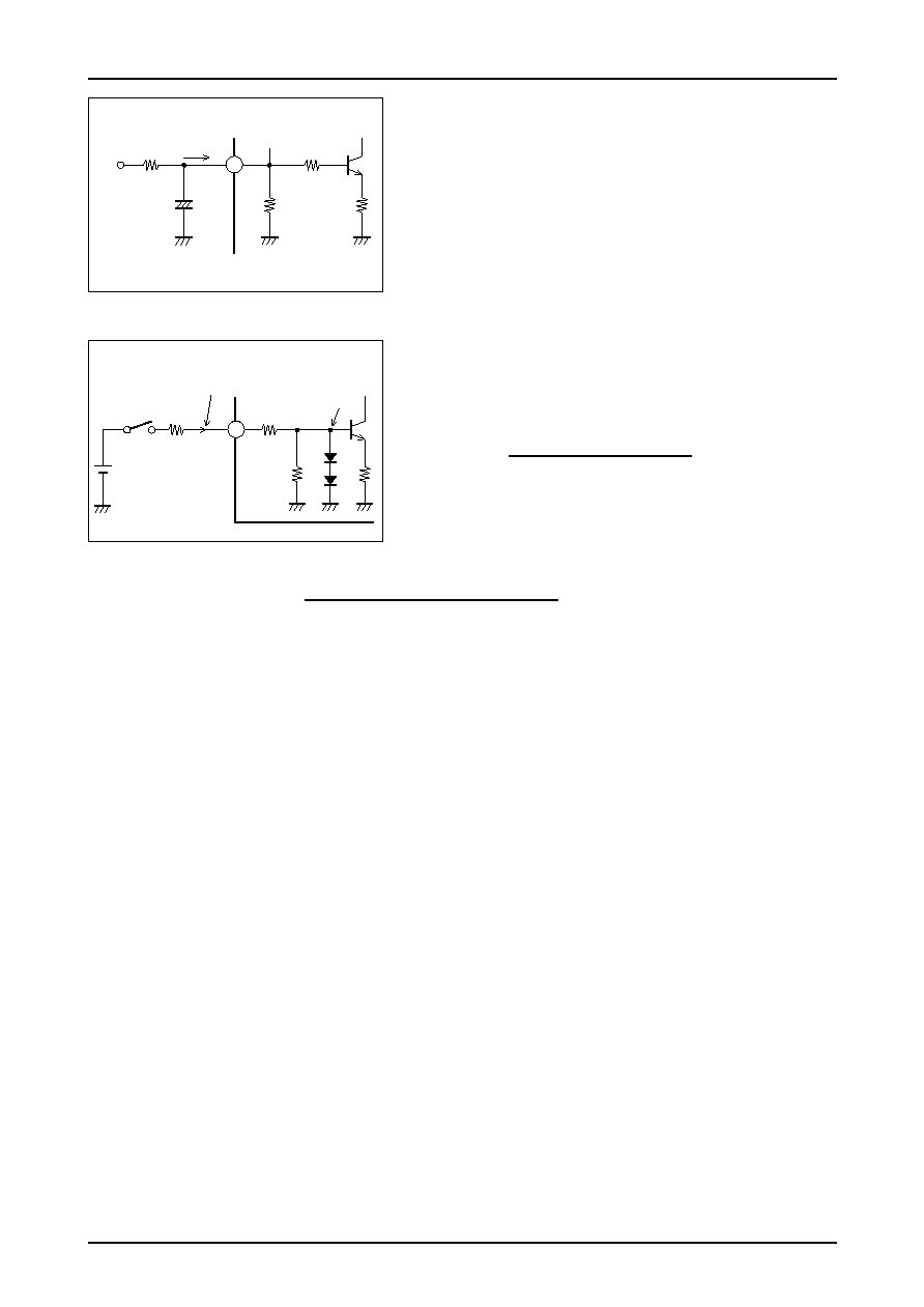
LA4632
When an voltage of +5 V is applied to the mute pin through the
external 15 k
resistor, the pin 6 voltage becomes about 1.85 V. (The
muting function activation level in the specifications is 1.7 V
minimum.) The pin 6 influx current (Imute) at this time will be
roughly 210 µA.
Although it is possible to change the mute pin applied voltage or the
values of the mute pin external components, if the pin 6 voltage (and
pin 6 influx current) is too high, or if the pin 6 external component
time constant is too short, the amplitude of impulse noise in the
system may rise. This phenomenon must be taken into account when
designing this circuit.
15k
+5V
2k
20k
10
µ
F
2k
6
Imute
Pin 6 IC internal equivalent circuit
Mute pin applied
voltage
Other items
Standby function
The IC's pin 5 is a standby pin. The amplifier is turned on when the
voltage applied to this pin is about 2 V or higher. (The value in the
specifications is 2.5 V minimum.) If a voltage of +5 V is directly
applied to the standby pin, the pin 5 influx current will be about 230
µA.
If a voltage that exceeds the upper limit voltage given in the
specifications (10 V) is applied as the standby pin voltage, calculate a
value for an external resistor R
STB
from the following formula so that
the pin 5 influx current does not increase excessively (use a value of under about 500 µA as the initial target value).
Usage Notes
Notes on the Maximum Ratings
If this IC is used in the vicinity of the maximum ratings, even the slightest fluctuations in the operating conditions could
cause those ratings to be exceeded, making the destruction of the device possible. Applications must be designed with
adequate margins in the supply voltage and other parameters so that the devices is always used in ranges that do not
exceed the maximum ratings.
Notes on Protection Circuits
While the LA4632 provides a full complement of built-in protection circuits, care is required in their use. In particular,
be careful not to inadvertently short IC pins to each other.
[Notes on the short to power, short to ground, and load shorting protection circuit]
∑ This protection circuit operates when an abnormal short such as a short to power (a short between an output and
V
CC
), a short to ground (a short between an output and ground), or a load short (a short between the output ± sides)
occurs. Although this circuit may not operate when the V
CC
voltage is under about 9 V, the thermal protection
circuit is thought adequate to protect the IC in that case.
∑ This protection circuit is the type that continues to operate while the above listed short state continues and recovers
automatically as soon as the abnormality is resolved. However, there are cases where, depending on the operating
conditions, the protection circuit locks and the protection operation continues. In these cases, the protection circuit
can be cleared by switching to standby mode or cutting and reapplying power.
∑ Note that if the output is shorted to power in the state where the IC is in the standby state (amplifier operation is
turned off) and V
CC
is over about 20 V, an offset may occur between the plus and minus outputs. If a load is
connected in this state, current may flow in through the load and the IC may be destroyed.
∑ In the following usage conditions, a symptom in which the output audio is cut off at high outputs due to protection
circuit operation. Depending on the end product specifications, it may be necessary to check for this phenomenon.
∑ Situations where both channels are operating in a manner that the I
O
Peak per channel exceeds 1 A at low RL (high
loads) and high V
CC
(The higher the chip temperature the easier it is for this phenomenon to occur.)
The "Allowable operating supply voltage range (V
CC
op)" item in the operating conditions specifications provides
specific target operating conditions so that the above phenomenon will not occur under severe usage conditions
(high temperatures, high outputs. (See the different V
CC
op ranges for different R
L
values.)
Use ISTB = up to 500
µ
A
as an initial target.
15k
Pin 5 IC internal equivalent circuit
Standby pin
applied voltage
2VBE
RSTB
1.5k
30k
5
ISTB =
= 230
µ
A
5 V ≠ 2 VBE (about 1.55 V)
15 k
RSTB =
≠ 15 k
Applied voltage - 2VBE (about 1.55 V)
ISTB (Under 500
µ
A)