 | –≠–ª–µ–∫—Ç—Ä–æ–Ω–Ω—ã–π –∫–æ–º–ø–æ–Ω–µ–Ω—Ç: LA4742 | –°–∫–∞—á–∞—Ç—å:  PDF PDF  ZIP ZIP |
Ordering number : ENN7043
92101TN (OT) No. 7043-1/9
Overview
The LA4742 is a 45 W 4-channel power amplifier IC for
car stereo systems. It features a built-in bridge circuit and
the ability to radically reduce the number of external
components required.
Features
∑ Maximum output power: 45 W
◊
4 channels
(V
CC
= 14.4 V, 4
load, 1 kHz)
∑ 40 W
◊
4 channels (V
CC
= 13.7 V, 4
load, 1 kHz)
∑ Requires only seven external components and does not
require an oscillation prevention RC circuit, a noise
filter, or a BS capacitor.
Functions
∑ Output offset detection function (DDL)
∑ Warning tone (beep) generation function
∑ Muting function
∑ Built-in standby switch
∑ Full complement of built-in protection circuits,
including protection from shorting to V
CC
, shorting to
ground, load shorting, overvoltages, and overheating.
∑ Maximum supply voltage before damage in the open
ground state: 16 V
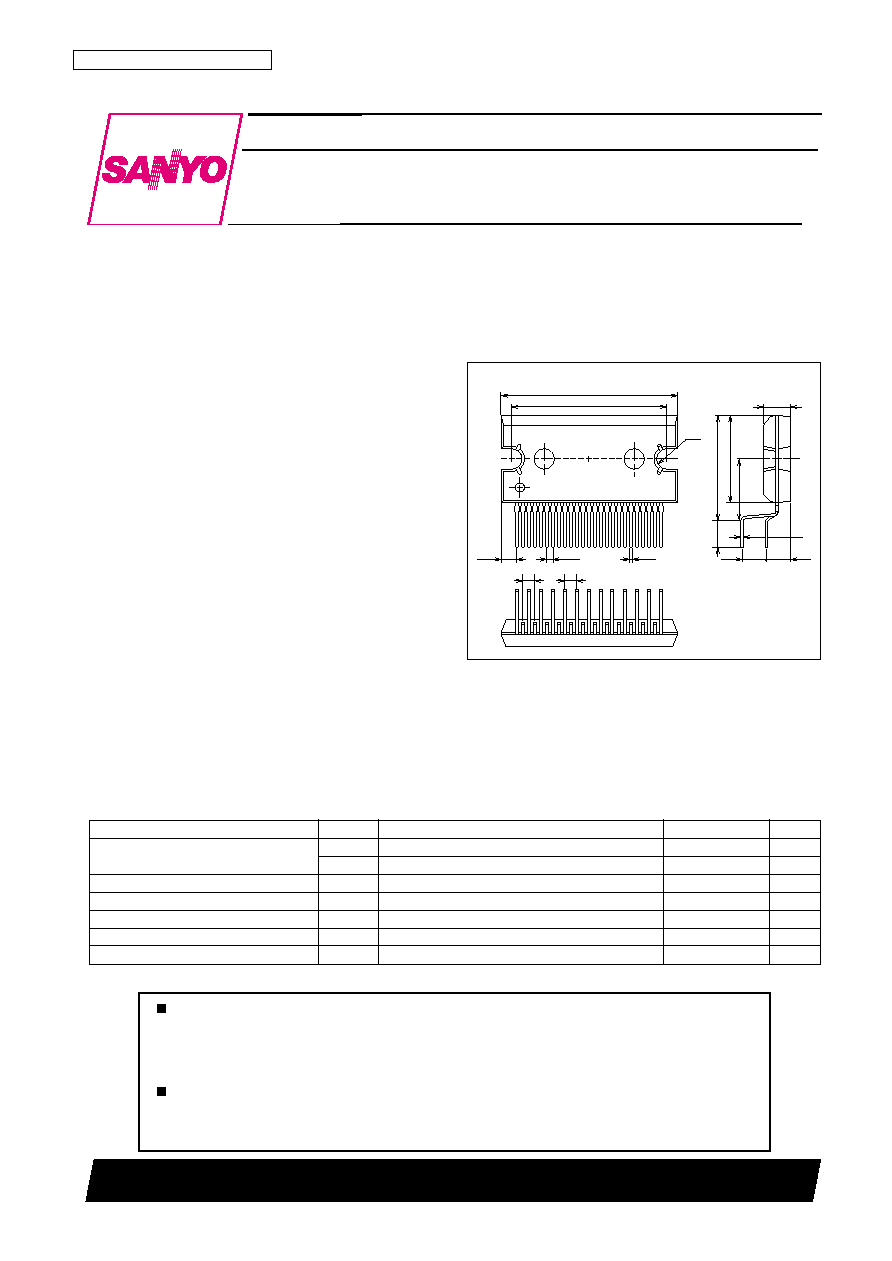
Package Dimensions
unit: mm
3236-HZIP25
2.0
2.0
29.2
2.60
(1.0)
25.6
0.53
R1.7
0.4
17.4
14.4
4.5
10.2
3.3
4.0
4.0
SANYO: HZIP25
[LA4742]
LA4742
SANYO Electric Co.,Ltd. Semiconductor Company
TOKYO OFFICE Tokyo Bldg., 1-10, 1 Chome, Ueno, Taito-ku, TOKYO, 110-8534 JAPAN
45 W Four-Channel (Bridge Circuit) Power Amplifier
Monolithic Linear IC
Any and all SANYO products described or contained herein do not have specifications that can handle
applications that require extremely high levels of reliability, such as life-support systems, aircraft's
control systems, or other applications whose failure can be reasonably expected to result in serious
physical and/or material damage. Consult with your SANYO representative nearest you before using
any SANYO products described or contained herein in such applications.
SANYO assumes no responsibility for equipment failures that result from using products at values that
exceed, even momentarily, rated values (such as maximum ratings, operating condition ranges, or other
parameters) listed in products specifications of any and all SANYO products described or contained
herein.
Parameter
Symbol
Conditions
Ratings
Unit
Maximum supply voltage
V
CC
max1
Signal present
18
V
V
CC
max2
No signal (for 1 minute)
26
V
Maximum output current
I
O
peak
4.5/ch
A
Allowable power dissipation
Pd max
With an arbitrarily large heat sink
50
W
Operating temperature
Topr
≠40 to +85
∞C
Storage temperature
Tstg
≠40 to +150
∞C
Package thermal resistance
jc
1
∞C/W
Specifications
Maximum Ratings
at Ta = 25∞C
No. 7043-2/9
LA4742
Parameter
Symbol
Conditions
Ratings
Unit
min
typ
max
Quiescent current
I
CCO
R
L
=
, Rg = 0
100
200
350
mA
Standby current
Ist
Vst = 0 V
10
µA
Output offset voltage
V
N
offset
Rg = 0
≠100
+100
mV
Voltage gain
VG
V
O
= 0 dBm
25
26
27
dB
Voltage gain difference
VG
≠1
+1
dB
P
O
1
THD = 10 %
23
28
W
Output power
P
O
max1
V
CC
= 13.7 V, V
IN
= 5 Vrms
40
W
P
O
max2
V
IN
= 5 Vrms
45
W
Total harmonic distortion
THD
P
O
= 4 W
0.05
0.4
%
Channel separation
CHsep
V
O
= 0 dBm, Rg = 10 k
55
65
dB
Ripple rejection ratio
SVRR
f
r
= 100 Hz, V
R
= 0 dBm, Rg = 0
50
60
dB
Output noise voltage
V
NO
Rg = 0, B.P.F. = 20 Hz to 20 kHz
100
200
µVrms
Muting attenuation
Mute(att)
V
O
= 20 dBm
70
80
dB
Operating Characteristics
at Ta = 25∞C, V
CC
= 14.4 V, f = 1 kHz, R
L
= 4
, Rg = 600
Parameter
Symbol
Conditions
Ratings
Unit
Recommended supply voltage
V
CC
14.4
V
Recommended load resistance
R
L
4
Operating supply voltage range
V
CC
op
9 to 18
V
Operating Conditions
at Ta = 25∞C
No. 7043-3/9
LA4742
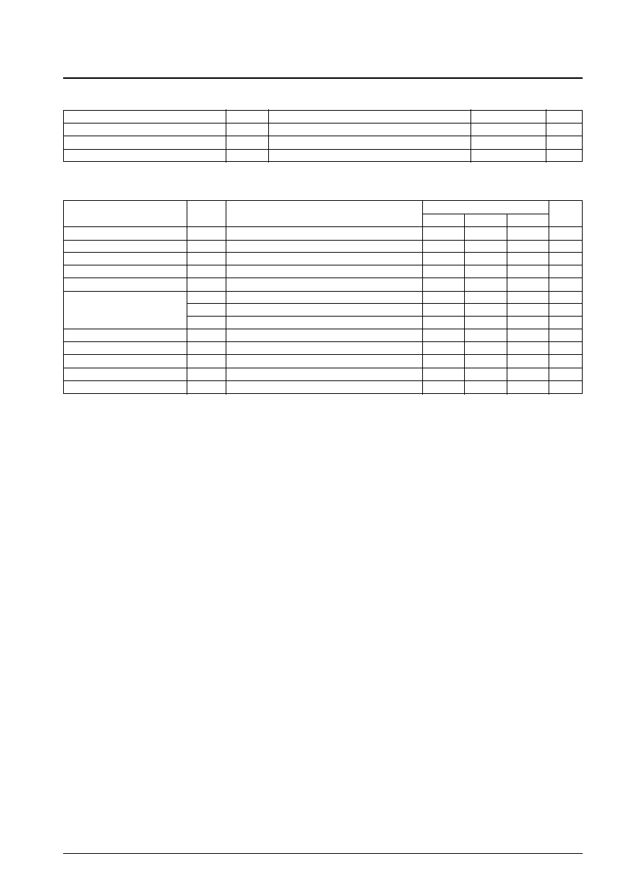
Sample Application Circuit and Block Diagram
9
11
6
20
7
25
8
5
3
12
2
4
22
10
17
15
19
1
18
13
21
23
14
24
16
Top view
OUT 1+
VCC1/2
VCC3/4
OUT 1≠
PWR GND 1
OUT 2+
OUT 2≠
PWR GND 2
Mute
OUT 3+
OUT 3≠
PWR GND 3
10k
OUT 4+
OUT 4≠
PWR GND 4
+
+
+
+
+
+
+
+
+
IN 1
CLIP DET
0.22
µ
F
IN 2
0.22
µ
F
3.3
µ
F
0.022
µ
F
IN 3
ST BY
0.22
µ
F
AUX IN
0.22
µ
F
IN 4
0.22
µ
F
47
µ
F
R.F
2200
µ
F
22
µ
F
PRE GND
ON TIME C
+
5V
Protective
Circuit
Stand by
Switch
Clip Detect
Circuit
Ripple
Filter
Mute
Circuit
Aux
Circuit
Low Level
Mute ON
Muting &
ON Time Control
Circuit
Protective
Circuit
≠
≠
+
+
+
≠
≠
+
+
≠
≠
+
+
+
≠
≠
A13765
+5V
ST ON
10k

No. 7043-4/9
LA4742
Pin Functions and Equivalent Circuits
at V
CC
= 14.4 V, ST-BY = 5 V
Pin No.
Function
DC voltage [V]
Notes
Internal equivalent circuit
1
AUX IN
2
8
18
24
POWER GND
3
130
Lowsaturation
voltage circuit
130
V
CC
5
7
9
17
19
21
23
A13766
3
5
7
9
17
19
21
23
≠OUT2
+OUT2
≠OUT1
+OUT1
+OUT3
≠OUT3
+OUT4
≠OUT4
2.7
∑ The amplifier will be on when the
applied voltage is between 2 V and
V
CC
.
4
ST-BY
10 k
30 k
1.5 k
4
A13767
6
20
V
CC
1/2
V
CC
3/4
∑ Low ripple power supply line for all
internal IC blocks
10
SVR
13.2
200
200
V
CC
1 k
10
A13768
Bias circuit ST-BY power
supply line
Input amplifier ST-BY
power supply line
Continued on next page.
No. 7043-5/9
LA4742
Continued from preceding page.
Pin No.
Function
DC voltage [V]
Notes
Internal equivalent circuit
11
12
14
15
IN1
IN2
IN4
IN3
100
1 k
Inverter
amplifier
Input amplifier
ST-BY power
supply line
5 pF
30 k
V
REF
11
12
14
15
A13769
∑ Amplifier turn-on time control circuit
∑ Impulse noise prevention circuit
∑ With a 22 µF capacitor, the turn-on
time will be 0.6 s.
16
ON TIME MUTE
20 k
10 k
2 k
13 k
40 k
2 k
200
V
REF
16
A13770
Bias circuit
power supply line
13
∑ The muting function is activated when
the applied voltage is under 1 V.
22
MUTE
4.1
3 k
1 k
7.5 k
10 k
100
100 k
V
REF
V
REF
22
A13771
Input amplifier
ST-BY power
supply line
Amplifier
bias circuit
3.1
∑ Input amplifiers that require no
capacitor in the input noise filter.
PRE GND
2.6
25
CLIPDET

No. 7043-6/9
LA4742
Notes on Usage and Handling
∑ Oscillator stabilization
In some cases, details of the printed circuit board layout may lead to induced parasitic oscillation. This oscillation can
be prevented by adding any one of the following components. Verify the optimal values for these capacitors by testing
in actual end products.
Technique 1 ... Connect Mylar capacitors (0.1 µF) between the BTL amplifier outputs.
Technique 2 ... Connect an RC circuit (2.2
and 0.1 µF in series) between each output and ground.
∑ Audio quality (low band)
The low-band frequency characteristics can be improved by adjusting the values of the input capacitors. The
recommended value is 2.2 µF.
∑ Impulse noise
The LA4742 includes a built-in impulse noise suppression circuit. However, further improvement can be achieved by
using the muting circuit. When first applying power, activate the muting function at the same time as applying power.
Then, after the output DC potential has stabilized, turn off the muting function. When turning off the power, first
activate the muting function and then turn off the power. Sample transient responses are attached (see the timing
charts).
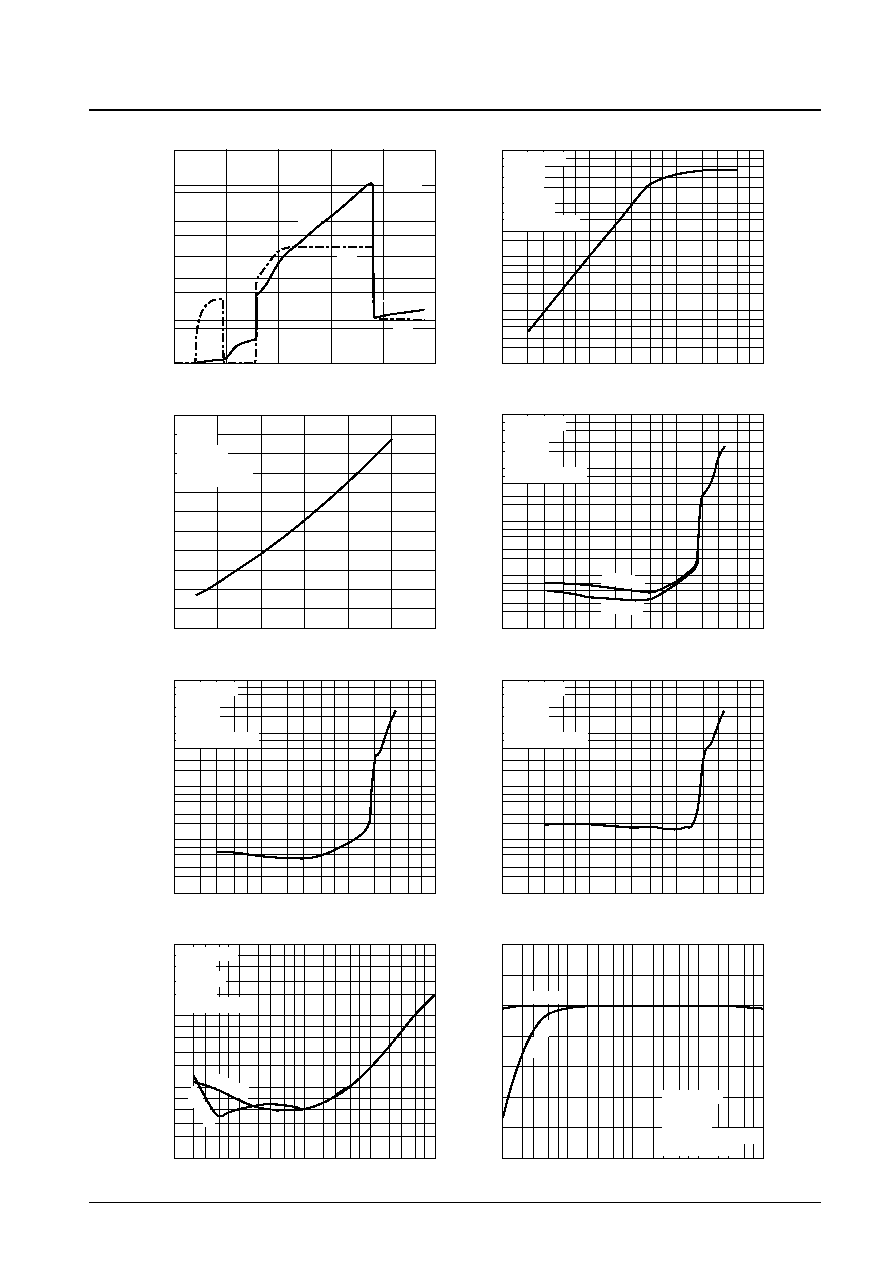
Transient Responses at Power On
Power on: Standby and muting activated at the same time.
Muting is turned off after the output has stabilized.
+
22
3.3
µ
F
Mute
10 k
MUTE OFF
ON TIME
MUTE
External 10 k
muting switch
Standby pin
Output pin
5 [V]
0
4
2
0
200 ms/div
0 [V]
5 [V]
Standby set high
Transient Responses at Power Off
Power off: After activating the muting circuit, turn the power off.
+
22
3.3
µ
F
Mute
10 k
MUTE
200 ms/div
5 [V]
0
4
2
0
0 [V]
5 [V]
External 10 k
muting switch
Standby pin
Output pin
Standby set low
No. 7043-7/9
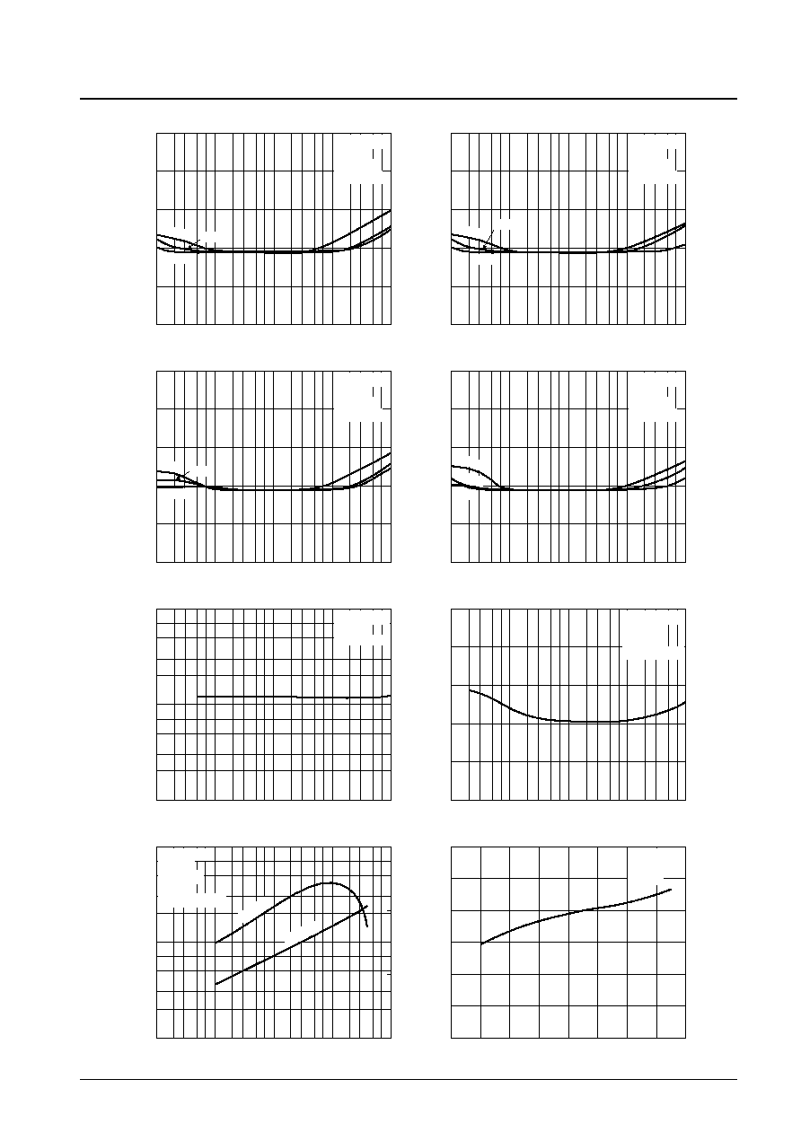
LA4742
50
0
100
150
200
250
300
0
5
10
15
20
25
2
3
5
7
0.1
2
3
5
7
1.0
2
3
5
7
10
2
3
5
7
100
0.01
1
0
2
3
4
5
10
2
3
5
7 100
2
3
5
7 1k
2
3
5
7 10k
8
12
16
4
20
24
28
32
36
40
44
48
8
10
12
14
16
18
20
2
3
5
7
0.1
2
3
5
7
1
2
3
5
7
10
2
3
5
7
100
0.01
0.1
2
3
5
7
1
2
3
5
7
10
2
3
5
7 100
2
3
5
7
0.1
2
3
5
7
1
2
3
5
7
10
2
3
5
7
100
0.01
0.1
3
5
7
1
2
3
5
7
10
2
3
5
7 100
2
2
3
5
7
0.1
2
3
5
7
1
2
3
5
7
10
2
3
5
7
100
0.01
0.1
2
3
5
7
1
2
3
5
7
10
2
3
5
7 100
≠10
≠8
≠6
≠4
≠2
0
2
4
10
I
CCO
, V
N
-- V
CC
I
CCO
I
CCO
V
N
V
N
0.22
µ
F
2.2
µ
F
OUT1, 3
OUT2, 4
OUT1, 3
OUT2, 4
P
O
-- V
IN
P
O
-- V
CC
R
L
=Open
Rg=0
Vst=5 V
THD -- P
O
THD -- P
O
f -- Response
THD -- f
V
CC
=14.4V
R
L
=4
f=1kHz
Rg=600
V
G
=26dB
All channels driven
V
CC
=14.4V
R
L
=4
f=100Hz
Rg=600
All channels driven
V
CC
=14.4V
R
L
=4
f=1kHz
Rg=600
All channels driven
V
CC
=14.4V
R
L
=4
Rg=600
P
O
=2W
All channels driven
V
CC
=14.4V
R
L
=4
Rg=600
V
O
=0 dBm at f = 1 kHz
ALL channels driven
V
CC
=14.4V
R
L
=4
f=10kHz
Rg=600
All channels driven
R
L
=4
f=1kHz
Rg=600
THD=10%
All channels driven
2
3
5
7
0.1
2
3
5
7
1
2
3
5
7
10
0.01
10
2 3
5 7 100
2 3
5 7 100 2 3 5 7 1k
2 3
5 7 10k
2 3
5 7100k
2 3
5 7 1k
2 3
5 7 10k
2 3
5 7100k
THD -- P
O
Quiescent current, I
CCO
-- V
Output power, P
O
-- W
Supply voltage, V
CC
-- V
Input level, V
IN
-- mVrms
Supply voltage, V
CC
-- V
Output power, P
O
-- W
Total harmonic distortion, THD -- %
Output power, P
O
-- W
Output pin voltage, V
N
-- V
Total harmonic distortion, THD -- %
Output power, P
O
-- W
Total harmonic distortion, THD -- %
Output power, P
O
-- W
Total harmonic distortion, THD -- %
Input frequency, f -- Hz
Response -- dB
Input frequency, f -- Hz
≠80
≠100
≠60
≠40
≠20
≠80
≠100
≠60
≠40
≠20
0
≠80
≠60
≠40
≠20
0
0
≠80
≠60
≠40
≠20
0
10
2 3
5 7 100 2 3 5 7 1k
2 3
5 7 10k
2 3
5 7100k
10
2 3
5 7 100 2 3 5 7 1k
2 3
5 7 10k
2 3
5 7100k
2 3
5 7 100 2 3 5 7 1k
2 3
5 7 10k
2 3
5 7
2 3
5 7
2 3
5 7
2 3
5 7
2 3
5 7
100k
100
1k
10k
100k
10
≠100
≠100
10
2
3
5
0.01
7
0.1
2
3
5
7
1
10
2 3
5 7100
2 3
5 7 1k
2 3
5 7 10k
2 3
5 7100k
≠100
≠80
≠60
≠40
≠20
0
10
2 3
5 7100
2 3
5 7 1k
2 3
5 710k
2 3
5 7100k
0
0.1
1
10
50
100
150
200
250
300
100
≠60
≠40
≠20
0
20
40
60
80
100
Channel separation, CH Sep -- dB
Channel separation, CH Sep -- dB
Channel separation, CH Sep -- dB
Ripple rejection ratio, SVRR -- dB
Quiescent current, I
CCO
-- mA
Power dissipation, Pd -- W
Output noise voltage, V
NO
-- mVrms
Current drain, I
CC
-- A
Input frequency, f -- Hz
Input frequency, f -- Hz
Input resistor, Rg --
Input frequency, f -- Hz
Ripple frequency, fr -- Hz
Ambient temperature, Ta --
∞
C
Output power, P
O
--
∞
C
Channel separation, CH Sep -- dB
Input frequency, f -- Hz
CH Sep -- f
1
2
2
1
2
3
2
4
1
3
1
4
3
1
3
2
Pd [W]
I CC
[A]
4
3
4
2
4
1
3
4
CH Sep -- f
CH Sep -- f
CH Sep -- f
V
NO
-- Rg
I
CCO
-- Ta
Pd, I
CC
-- P
O
1
2
3
5
7
10
2
3
5
7
100
0.01
2 3
5 7 0.1
2 3
5 7 1
2 3
5 7 10
2 3
5 7 100
SVRR -- fr
V
CC
=14.4V
R
L
=4
Rg=10k
V
O
=0dBm
V
CC
=14.4V
R
L
=4
Rg=10k
V
O
=0dBm
V
CC
=14.4V
R
L
=4
DIN AUDIO
V
CC
=14.4V
R
L
=4
Rg=10k
V
O
=0dBm
V
CC
=14.4V
R
L
=4
Rg=0
V
CCR
=0dBm
V
CC
=14.4V
R
L
=OPEN
Rg=0
V
CC
=14.4V
R
L
=4
Rg=10k
V
O
=0dBm
V
CC
=14.4V
R
L
=4
Rg=600
f=1kHz
All channels driven
No. 7043-8/9
LA4742
PS No. 7043-9/9
LA4742
This catalog provides information as of September, 2001. Specifications and information herein are
subject to change without notice.
Specifications of any and all SANYO products described or contained herein stipulate the performance,
characteristics, and functions of the described products in the independent state, and are not guarantees
of the performance, characteristics, and functions of the described products as mounted in the customer's
products or equipment. To verify symptoms and states that cannot be evaluated in an independent device,
the customer should always evaluate and test devices mounted in the customer's products or equipment.
SANYO Electric Co., Ltd. strives to supply high-quality high-reliability products. However, any and all
semiconductor products fail with some probability. It is possible that these probabilistic failures could
give rise to accidents or events that could endanger human lives, that could give rise to smoke or fire,
or that could cause damage to other property. When designing equipment, adopt safety measures so
that these kinds of accidents or events cannot occur. Such measures include but are not limited to protective
circuits and error prevention circuits for safe design, redundant design, and structural design.
In the event that any or all SANYO products (including technical data, services) described or contained
herein are controlled under any of applicable local export control laws and regulations, such products must
not be exported without obtaining the export license from the authorities concerned in accordance with the
above law.
No part of this publication may be reproduced or transmitted in any form or by any means, electronic or
mechanical, including photocopying and recording, or any information storage or retrieval system,
or otherwise, without the prior written permission of SANYO Electric Co., Ltd.
Any and all information described or contained herein are subject to change without notice due to
product/technology improvement, etc. When designing equipment, refer to the "Delivery Specification"
for the SANYO product that you intend to use.
Information (including circuit diagrams and circuit parameters) herein is for example only; it is not
guaranteed for volume production. SANYO believes information herein is accurate and reliable, but
no guarantees are made or implied regarding its use or any infringements of intellectual property rights
or other rights of third parties.
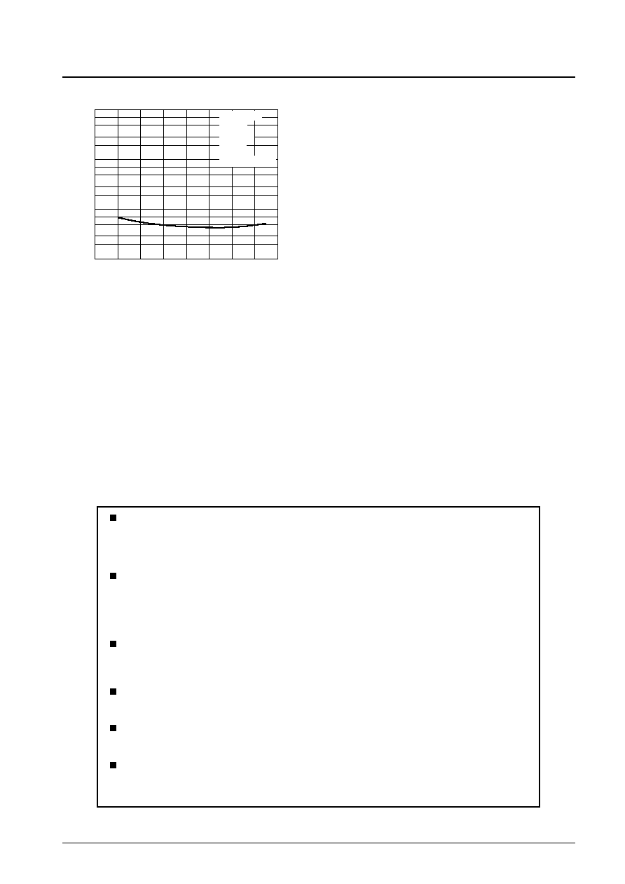
0.01
2
3
5
7
0.1
2
3
5
7
1
2
3
5
7
10
≠60
≠40
≠20
0
20
40
60
80
100
Ambient temperature, Ta --
∞
C
Total harmonic distortion, THD -- %
THD -- Ta
V
CC
=14.4V
R
L
=4
Rg=600
f=1kHz
P
O
=2W
All channels driven