 | –≠–ª–µ–∫—Ç—Ä–æ–Ω–Ω—ã–π –∫–æ–º–ø–æ–Ω–µ–Ω—Ç: LA4800 | –°–∫–∞—á–∞—Ç—å:  PDF PDF  ZIP ZIP |
3 V Stereo Headphone Power Amplifier
Overview
The LA4800V is a headphone stereo power amplifier IC that
features a high signal-to-noise ratio, high ripple rejection, low
distortion and low current consumption, making it ideal for
portable CD players.
Functions
.
Headphone stereo power amplifier
.
Beep tone
.
Power switch
.
Power mute switch
Features
.
96 dB (typ) high S/N ratio at 7 µV
.
76 dB (typ) high ripple rejection
.
0.07% (typ) low distortion with R
L
= 16
.
6.2 mA (typ) low current consumption
.
Outputs do not require electrolytic capacitors.
.
Available in 16-pin SSOPs
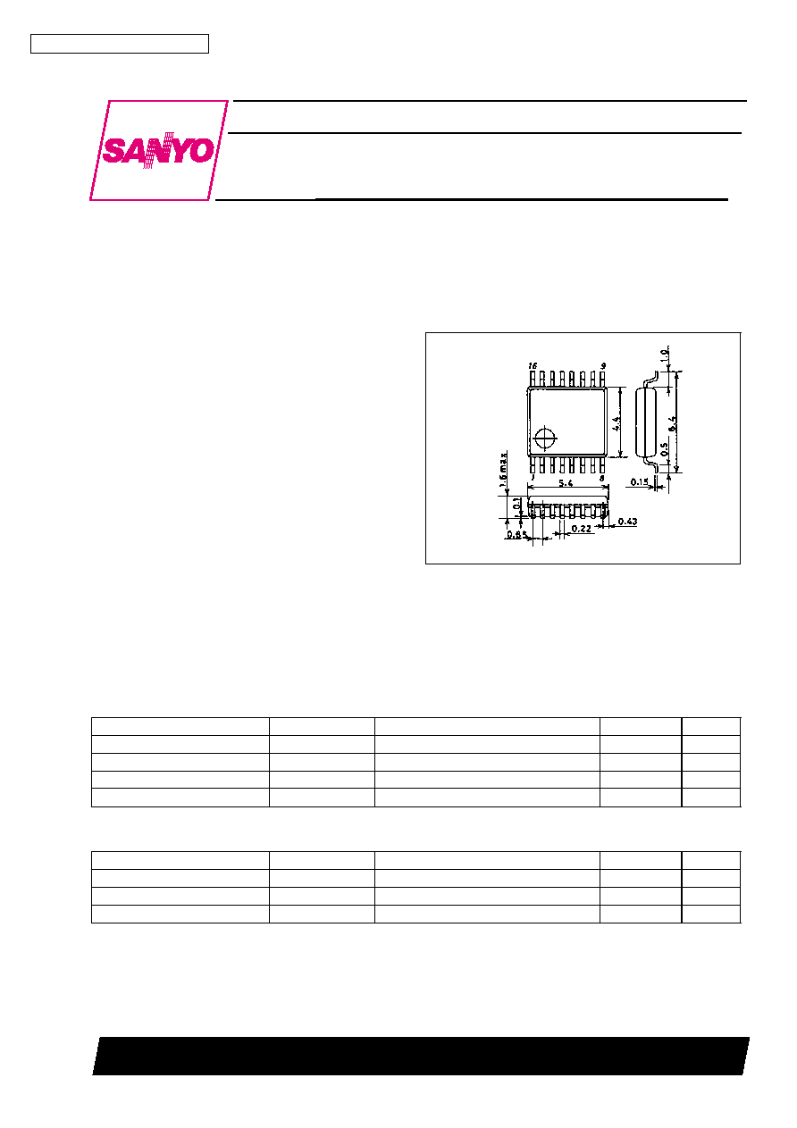
Package Dimensions
unit : mm
3178-SSOP16
[LA4800V]
SANYO : SSOP16
Specifications
Maximum Ratings
at Ta = 25∞C
Parameter
Symbol
Conditions
Ratings
Unit
Maximum supply voltage
V
CC
max
4.5
V
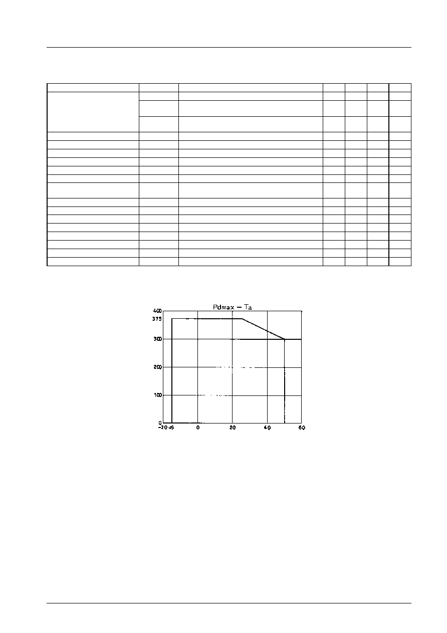
Power dissipation
Pd max
375
mW
Operating temperature range
Topr
≠15 to 50
∞C
Storage temperature range
Tstg
≠40 to 150
∞C
Recommended Operating Ranges
at Ta = 25∞C
Parameter
Symbol
Conditions
Ratings
Unit
Supply voltage
V
CC
3.0
V
Load resistance
R
L
16 to 32
Operating supply voltage range
V
CC
op
1.8 to 3.6
V
Ordering number: EN4335A
Monolithic Linear IC
LA4800V
SANYO Electric Co.,Ltd. Semiconductor Bussiness Headquarters
TOKYO OFFICE Tokyo Bldg., 1-10, 1 Chome, Ueno, Taito-ku, TOKYO, 110 JAPAN
32896HA(II)/60393TS No.4335-1/11
Operating Characteristics
at Ta = 25∞C, V
CC
= 2.5 V, R
L
= 16
, f = 1 kHz unless otherwise noted.
Values in parentheses indicate V
CC
= 3.0 V
Parameter
Symbol
Conditions
min
typ
max
Unit
Quiescent supply current
I
CCO1
IC OFF
0.05
1.0
µA
I
CCO2
Mute ON
1.6
(1.65)
3.0
mA
I
CCO3
No input signal
6.2
(6.8)
9.0
mA
Voltage gain
VG
V
O
= ≠10 dBm
10.3
11.8
13.3
dB
Channel balance
V
RL
V
O
= ≠10 dBm
≠1
0
1
dB
Output power
P
O
V
CC
= 3.0 V, THD = 10%
15
25
mW
Total harmonic distortion
THD
V
O
= 0.35 V
0.075
0.2
%
Output noise voltage
V
NO
Rg = 1 k
, DIN AUDIO
7.8
15
µV
Crosstalk
CT
f = 1 kHz, TUN, V
O
= ≠10 dBm
35
45
dB
Ripple rejection
R.R
V
CC
= 1.7 V, f = 100 Hz, V
CR
= ≠20 dBm,
TUN = 100 Hz
65
76
dB
Mute attenuation
V
OFF
THD = 1%
≠80
≠96
dB
Beep tone output voltage
V
O BEEP
V
I
= ≠13.5 dBm (sine wave)
1.5
3.0
mV
Output DC offset voltage
V
DC OFF
V
I
= 0 V, Rg = 1 k
≠20
0
20
mV
Power ON current sensitivity
l
1 ON
V
CC
= 1.7 V, V
5
^
1.0 V
50
60
µA
Power OFF voltage sensitivity
V
1 OFF
V
CC
= 1.7 V, V
5
%
0.1 V
0.5
0.6
V
Mute OFF current sensitivity
l
16 OFF
V
CC
= 1.7 V, V
5
^
1.0 V
4.5
6.0
µA
Mute OFF voltage sensitivity
V
16 OFF
V
CC
= 1.7 V
1.0
1.25
1.5
V
Mute ON voltage sensitivity
V
16 ON
V
CC
= 1.7 V
0.9
1.0
V
Maximum
power
dissipation,
Pd
max
-
m
W
Ambient temperature, Ta - ∞C
LA4800V
No.4335-2/11
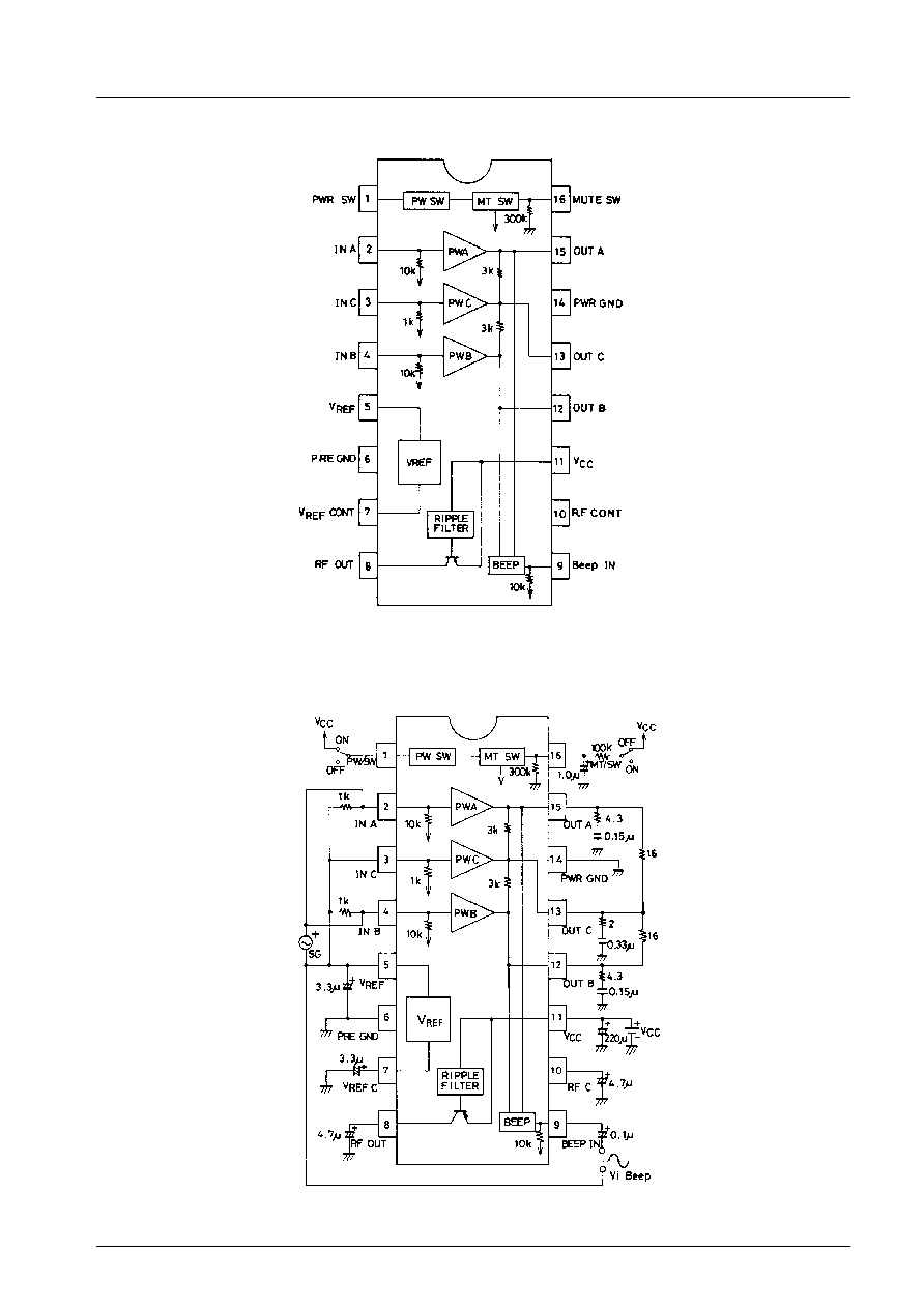
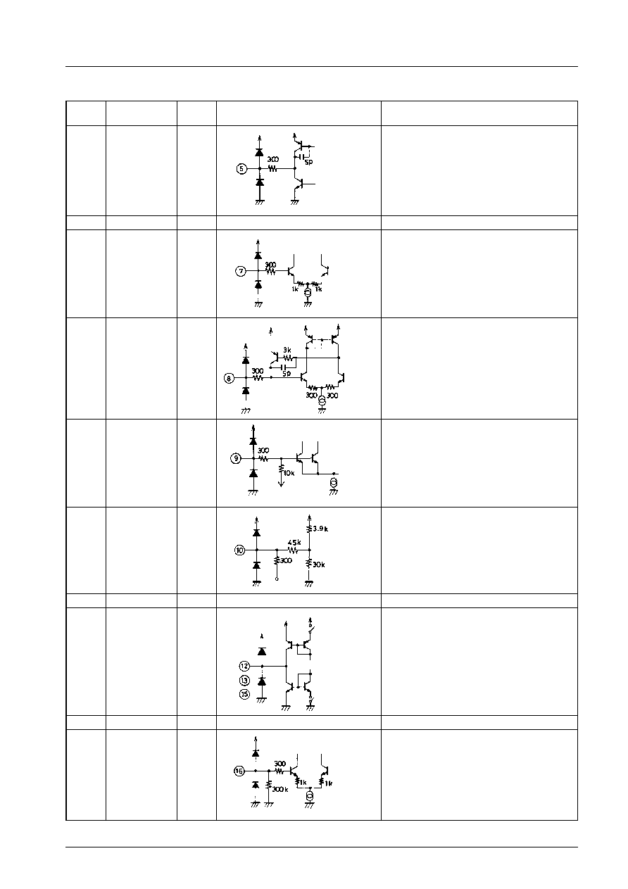
Pin Assignment and Block Diagram
Test Circuit
Top view
Unit (resistance:
)
Unit (resistance:
, capacitance: F)
LA4800V
No.4335-3/11
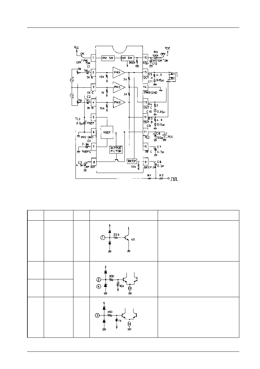
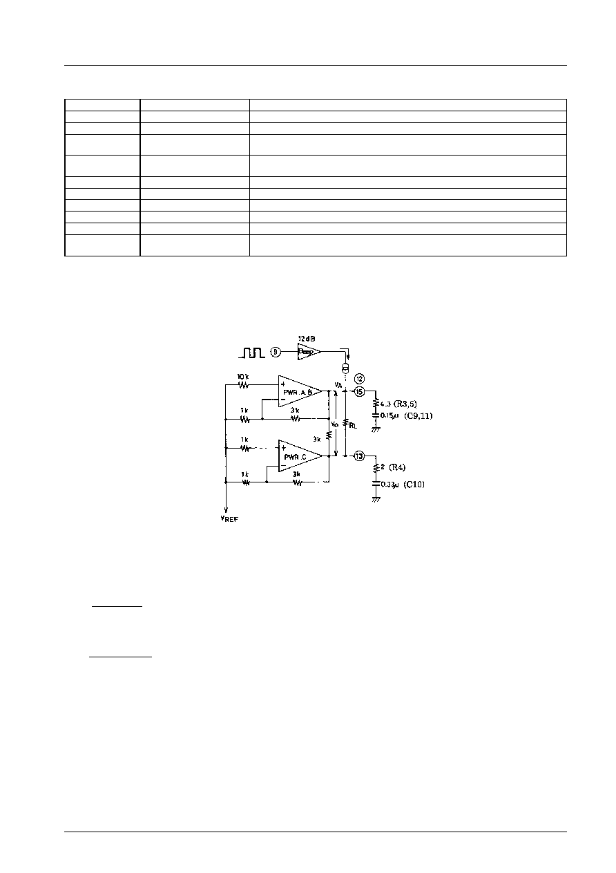
Sample Application Circuit
Pin Description
V
CC
= 2.5 V
Unit (resistance:
)
Pin
number
Pin name
V
DC
(V)
Equivalent circuit
Pin description
1
PWR SW
0 to 0.7
Power switch
Turns ON the power to the V
CC
pin.
2
IN A
1.1
Power input pins
10 k
input resistance
4
IN B
3
IN C
1.1
Power amplifier common input pin
Usually connected to Vref
Continued on next page.
Signal from microcontroller
Unit (resistance:
, capacitance: F)
LA4800V
No.4335-4/11
Continued from preceding page.
Unit (resistance:
)
Pin
number
Pin name
V
DC
(V)
Equivalent circuit
Pin description
5
V
REF
OUT
1.1
F
1.1 V fixed bias
6
PRE GND
Preamplifier ground
7
V
REF
CONT
1.1
1.1 V reference control pin
8
RF OUT
2.2
F
Preset to approximately V
CC
◊
0.88 V
9
Beep IN
1.1
Beep tone input pin
Active only when mute is ON.
10
RF CONT
2.2
to RF
RF control pin
11
V
CC
Power supply
12
13
15
OUT B
OUT C
OUT A
1.1
1.1
1.1
Power output pins
Pin 13 is the headphone center common drive.
(No electrolytic capacitors required)
14
PWR GND
Power amplifier ground
16
MUTE SW
0 to 1.85
The mute pin is floating when ON, and tied to
V
CC
through a 100 k
when OFF.
LA4800V
No.4335-5/11
External Components Description
Components
Recommended value
Description
C1, C2
1 to 4.7 µF
Input coupling capacitors
C3, C4
3.3 to 10 µF
Reference bias (V
REF
) decoupling capacitors
C5, C4
4.7 to 10 µF
Ripple filter capacitors. Increasing the capacitance also increases the distortion and
the supply rise time at turn ON.
C6
0.1 to 1 µF
Input coupling capacitor for the beep tone. Choose a value that does not attenuate the
beep tone signal.
C8
220 µF
Supply line coupling capacitor
C9, C10, C11
0.22 to 0.47 µF
Oscillation damping capacitors. Film capacitors are recommended.
C12
0.1 to 1.0µF
Mute time setting capacitor. See the description in the Operating Notes.
R1, R2
Beep tone input signal adjustment resistors. Follow the manufactures instructions.
R3, R4, R5
0.5 to 4.3
Power amplifier oscillation damping resistors.
R6
100 k
Mute OFF pin 16 bias setting resistor. The internal 300 k
resistor and this 100 k
resistor together set the mute switch (pin 16) threshold.
Operating Notes
Beep tone operating principle
The design of the above when mute is ON (pin 16 open) is as follows:
The output voltage V
O
as function of R
L
is
V
O
=
R
L
R
L
+ 3k+ 1k
◊
V
A
For example, if R
L
= 16
and V
A
= 0.5 V (V
A
is the adjusted input voltage on pin 9),
V
O
=
16
16
+ 3k+ 1k
◊
0.5
2 mV
The beep tone output voltage V
O
is determined by the above equation. However, the oscillation damping RC components are
connected to the PWR output and hence these RC components will also influence the actual value of V
O
. When using the beep
tone, the impedance of C10, connected to the common output (pin 13), must be greater than the impedance of C9 and C11, i.e.
C10 must be greater than C9 and C11.
Signal from microcontroller
Unit (resistance:
, capacitance: F)
LA4800V
No.4335-6/11

Mute time adjustment
The mute ON/OFF switching waveforms are shown in the figure above. The settling time t
S
is determined by the capacitor C
r
connected to pin 16. The recommended value of C
r
is 1 µF. If the value used is less than 1 µF, pop noise will increase.
The setting time for different values of C
r
are shown in the table below.
C
r
(µF)
t
S OFF
(ms)
t
S ON
(ms)
0.1
15
3.2
1.0
150
30
2.2
300
56
LA4800V
No.4335-7/11
Quiescent
current,
I
CCO
-m
A
Mute
current,
I
MUTE
-m
A
Supply voltage, V
CC
- V
V
oltage
gain,
VG
-
d
B
Channel 2 ON
Unit (capacitance: F)
Input frequency, fi - Hz
I
CCO
STBY
-µ
A
V
oltage
gain,
VG
-
d
B
Supply voltage, V
CC
- V
T
otal
harmonic
distortion,
THD
-
%
Channel 2 ON
Input voltage, V
IN
- dBm
B.P.F = 400 Hz to 80 kHz
T
otal
harmonic
distortion,
THD
-
%
Supply voltage, V
CC
- V
Output
power
,
P
O
-m
W
Supply voltage, V
CC
- V
Channel 2 ON
B.P.F = 400 Hz to 80 kHz
Output
noise
voltage,
V
NO
-µ
V
Supply voltage, V
CC
- V
Crosstalk,
CT
-
d
B
Input frequency, fi - Hz
LA4800V
No.4335-8/11
Beep
tone
output
voltage,
V
O
Beep
-
m
V
Input voltage, V
IN
- dB
Unit (resistance =
, capacitance = F)
Beep
tone
output
voltage,
V
O
Beep
-
m
V
Input frequency, fi - Hz
Beep
tone
output
voltage,
V
O
Beep
-
m
V
Supply voltage, V
CC
- V
Ripple
rejection
ratio,
SVRR
-
d
B
Mute OFF
Mute ON
Supply voltage, V
CC
- V
Ripple
rejection
ratio,
SVRR
-
d
B
Supply voltage, V
CC
- V
Unit (resistance =
)
t
ON
,t
OFF
-s
C
MUTE
- µF
Pin
16
voltage,
V
CONT
1
6-V
Mute ON/OFF threshold region
Mute OFF
(PWR ON)
Mute ON
(PWR OUT = 80 dB)
Quiescent
current,
I
CCO
-m
A
Ambient temperature Ta - ∞C
Supply voltage, V
CC
- V
Mute OFF, 100k
, 1 µF (pin 16)
I
CCO
STBY
-µ
A
LA4800V
No.4335-9/11
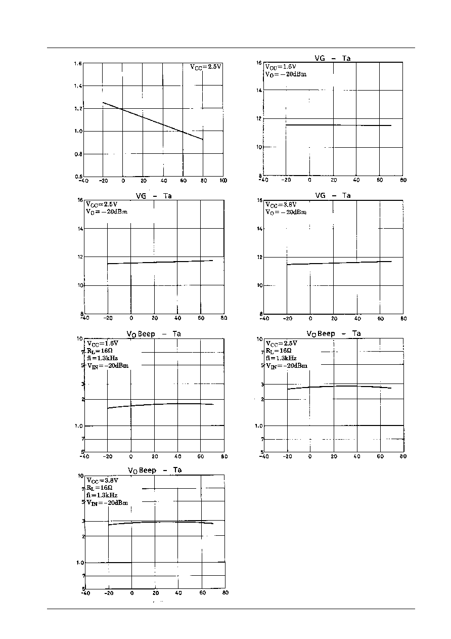
DC
voltage,
V
ref
DC
-
V
Ambient temperature, Ta - ∞C
V
oltage
gain,
VG
-
d
B
R
L
= 16
Headphone load
Ambient temperature, Ta - ∞C
Vref DC - Ta
V
oltage
gain,
VG
-
d
B
R
L
= 16
Headphone load
Ambient temperature, Ta - ∞C
V
oltage
gain,
VG
-
d
B
R
L
= 16
Headphone load
Ambient temperature, Ta - ∞C
Beep
tone
voltage,
V
O
Beep
-
m
V
Ambient temperature, Ta - ∞C
Beep
tone
output
voltage,
V
O
Beep
-
m
V
(sine wave)
(sine wave)
Ambient temperature, Ta - ∞C
Beep
tone
output
voltage,
V
O
Beep
-
m
V
(sine wave)
Ambient temperature, Ta - ∞C
LA4800V
No.4335-10/11

No products described or contained herein are intended for use in surgical implants, life-support systems, aerospace equipment,
nuclear power control systems, vehicles, disaster/crime-prevention equipment and the like, the failure of which may directly or
indirectly cause injury, death or property loss.
Anyone purchasing any products described or contained herein for an above-mentioned use shall:
1
Accept full responsibility and indemnify and defend SANYO ELECTRIC CO., LTD., its affiliates, subsidiaries and distributors
and all their officers and employees, jointly and severally, against any and all claims and litigation and all damages, cost and
expenses associated with such use:
2
Not impose any responsibility for any fault or negligence which may be cited in any such claim or litigation on SANYO
ELECTRIC CO., LTD., its affiliates, subsidiaries and distributors or any of their officers and employees jointly or severally.
Information (including circuit diagrams and circuit parameters) herein is for example only; it is not guaranteed for volume
production. SANYO believes information herein is accurate and reliable, but no guarantees are made or implied regarding its use
or any infringements of intellectual property rights or other rights of third parties.
This catalog provides information as of March, 1996. Specifications and information herein are subject to change without notice.
LA4800V
No.4335-11/11