 | –≠–ª–µ–∫—Ç—Ä–æ–Ω–Ω—ã–π –∫–æ–º–ø–æ–Ω–µ–Ω—Ç: LA4802T | –°–∫–∞—á–∞—Ç—å:  PDF PDF  ZIP ZIP |
Ordering number : ENN6657
72502RM (OT) No. 6657-1/10
Overview
The LA4802T is a headphone stereo power amplifier for
portable CD and MD players. It features a high signal-to-
noise ratio, a high ripple rejection ratio, low distortion,
and low current drain.
Functions
∑ Headphone stereo power amplifier
∑ Power switch
∑ Muting switch
∑ Beep tone function control input pin (The beep tone
function can be used regardless of whether the mute
function is on or off.)
Features
∑ High signal-to-noise ratio (100 dB typical at 7.5 µV)
∑ High ripple rejection ratio (70 dB typical)
∑ Low current drain (950 µA typical)
∑ On-chip bass compensation circuit
(Compensates for bass frequency attenuation due to the
output capacitors and achieves flat frequency
characteristics.)
∑ Ultraminiature package (MSOP-20)
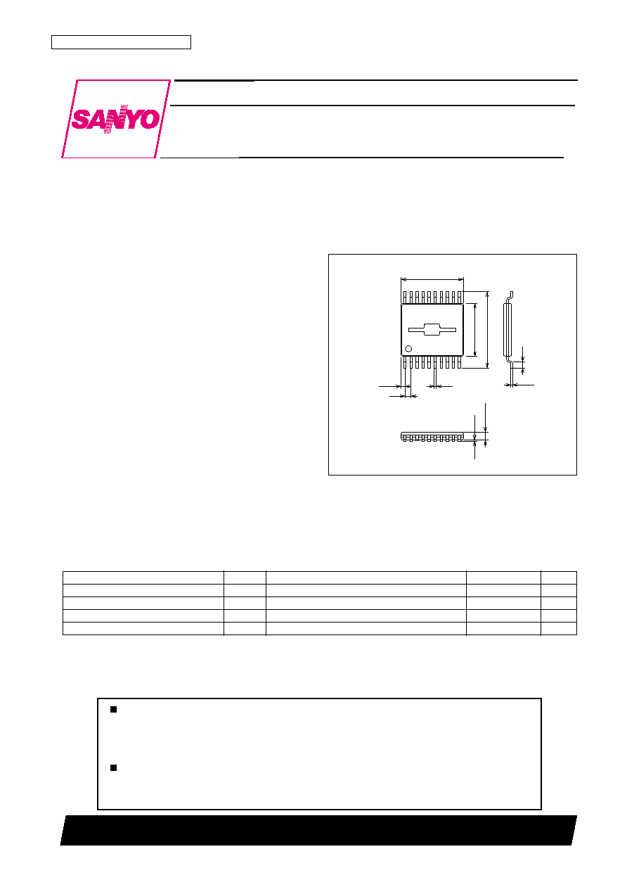
Package Dimensions
unit: mm
3262-MSOP20
6.3
5.2
0.5
4.4
(0.35)
(0.65)
0.5
0.125
1
10
20
11
0.2
0.08
0.85max
SANYO: MSOP20
[LA4802T]
LA4802T
SANYO Electric Co.,Ltd. Semiconductor Company
TOKYO OFFICE Tokyo Bldg., 1-10, 1 Chome, Ueno, Taito-ku, TOKYO, 110-8534 JAPAN
Headphone Stereo Power Amplifier
Monolithic Linear IC
Any and all SANYO products described or contained herein do not have specifications that can handle
applications that require extremely high levels of reliability, such as life-support systems, aircraft's
control systems, or other applications whose failure can be reasonably expected to result in serious
physical and/or material damage. Consult with your SANYO representative nearest you before using
any SANYO products described or contained herein in such applications.
SANYO assumes no responsibility for equipment failures that result from using products at values that
exceed, even momentarily, rated values (such as maximum ratings, operating condition ranges, or other
parameters) listed in products specifications of any and all SANYO products described or contained
herein.
Parameter
Symbol
Conditions
Ratings
Unit
Maximum supply voltage
V
CC
max
4.5
V
Allowable power dissipation
Pd max
When mounted, Ta = 80∞C
375
mW
Operating temperature
Topr
≠20 to +80
∞C
Storage temperature
Tstg
≠40 to +150
∞C
Specifications
Maximum Ratings
at Ta = 25∞C
No. 6657-2/10
LA4802T
Parameter
Symbol
Conditions
Ratings
Unit
Recommended supply voltage
V
CC
2.4
V
Operating supply voltage range
V
CC
op
1.8 to 3.6
V
Recommended load resistance
R
L
16 to 32
Operating Conditions
at Ta = 25∞C
Item
Symbol
Conditions
Ratings
Unit
min
typ
max
Quiescent current
I
CCO
1
Current when ST is off (with L.B. on and muting off)
0.05
1
µA
I
CCO
2
Current when muting is on (with ST on and L.B. on)
530
900
µA
I
CCO
3
Current when ST is on (with L.B. on and muting off)
950
1500
µA
Operating current drain
I
CC
1
P
O
= 0.1 mW (With 2 channels driven)
3.2
3.7
mA
Voltage gain
VG
V
O
= ≠10 dBm
6.8
7.8
8.8
dB
Channel balance
VG
V
O
= ≠10 dBm
≠1
0
+1
dB
Output power
P
O
THD = 10%
25
38
mW
Total harmonic distortion
THD
V
O
= ≠8 dBm, 20 kHz LPF
0.03
0.1
%
Output noise voltage
V
NO
Rg = 10 k
, IHF A
≠100
≠90
dBm
Crosstalk
CT
T
UN
1kHz, V
O
= ≠10 dBm
70
80
dB
Ripple rejection ratio
SVRR
fr = 100 kHz, Vr = ≠20 dBm, T
UN
100Hz
60
70
dB
Peak output voltage
V
O
BEEP
V
IN
= 2.4 Vp-p, f = 1 kHz, MUTE OFF
1.0
2.7
mV
Muting attenuation
V
OFF
THD = 1%, T
UN
1kHz
≠100
≠120
dB
Power on voltage sensitivity
V
1 ON
Power on threshold voltage
1.6
V
Power off voltage sensitivity
V
1 OFF
Power off threshold voltage
0.5
V
Mute on voltage sensitivity
V
20 ON
Muting on threshold voltage
1.4
V
Mute off voltage sensitivity
V
20 OFF
Muting off threshold voltage
0.5
V
Boost on voltage sensitivity
V
4 ON
Boost on threshold voltage
0.5
V
Boost off voltage sensitivity
V
4 OFF
Boost off threshold voltage
1.4
V
Ta = 25∞C, V
CC
= 2.7 V, f
IN
= 1 kHz, R
L
= 47 k
(Characteristics when used as a line output), L.B OFF
Operating current drain
I
CC
2
V
O
= 0 dBm (With 2 channels driven)
1.5
2.0
mA
Total harmonic distortion
THD2
V
O
= 0 dBm, 20 kHz LPF
0.005
0.05
%
Output noise voltage
V
NO
2
Rg = 10 k
, IHF A
≠100
≠90
dBm
Crosstalk
CT2
T
UN
1kHz, V
O
= ≠10 dBm
80
90
dB
Ripple rejection ratio
SVRR2
fr = 100 kHz, Vr = ≠20 dBm, T
UN
100Hz
65
78
dB
Electrical Characteristics
at Ta = 25∞C, V
CC
= 2.4 V, f
IN
= 1 kHz, R
L
= 16
Switch Threshold Voltages and Pin Influx Currents
∑ Standby switch (pin 1)
H : IC ON
L : IC OFF
Pin influx current (
µ
A)
0
20
40
60
80
100
120
0
1
2
3
4
5
V
1
(V)
H
L
∑ Mute switch (pin 20), boost switch (pin 4)
Pin influx current (
µ
A)
0
20
40
0
30
0
1
2
3
4
5
V
20
, V
4
(V)
H
L
H : MUTE ON, L. B OFF
L : MUTE OFF, L. B ON

No. 6657-3/10
LA4802T
Notes on the Beep Tone Output Function
∑ This function provides a beep tone output under control of the system microcontroller.
∑ The beep tone can be provided regardless of the on/off state of the muting function.
∑ The recommended beep input signal level is a square wave with V
IN
= 2.4 Vp-p. When the muting function is off, the
beep tone output, V
O
BEEP, will be 2.7 V rms, and when muting is on, the output will be 1.3 Vrms.
Notes on the Muting Time
∑ The muting on time and the muting off time can be modified by changing the value of the external capacitor C4
connected to pin 6. The recommended value for C4 is 1 µF. With lower values, impulse noise levels will increase.
∑ The on/off times will change as shown below when the value of C4 is varied.
C4
On time
Off time
0.1 µF
0.2 ms
9 ms
0.47 µF
1 ms
40 ms
1 µF
2 ms
80 ms
∑ We recommend operating the mute switch at the same time as the power on/off switch (pin 1) to minimize impulse
noise at power on and off.
VCC
MUTE S. W
PWR S. W
A13553
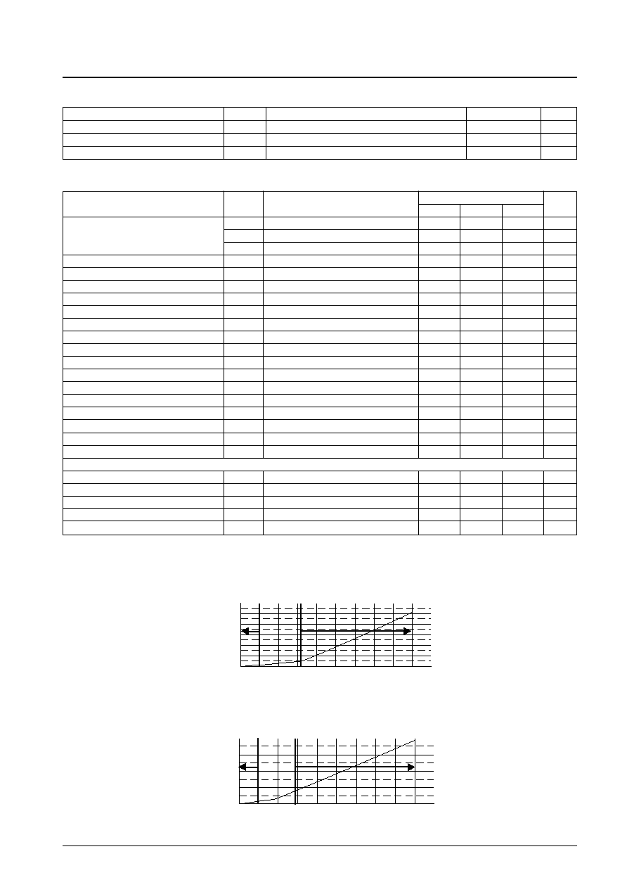
Notes on the Bass Compensation Circuit
∑ When the headphone load is connected to the output, the low frequencies will be attenuated due to the output
capacitors. This circuit compensates for that attenuation and creates frequency response characteristics that are close
to flat.
∑ This function can be turned on or off from pin 4. When used as a line output, the load will be less than 16
, and the
bass frequency characteristics will be somewhat increased. Therefore we recommend leaving the bass compensation
circuit off in this case.
A13554
+
Output pin
Load terminal
≠14
≠12
≠10
≠8
≠6
≠4
≠2
0
2
≠16
10
100
1000
1k
10k
VG -- f
Frequency, f -- Hz
No bass compensation
Bass compensation applied
Voltage gain, VG -- dB
No. 6657-4/10
LA4802T
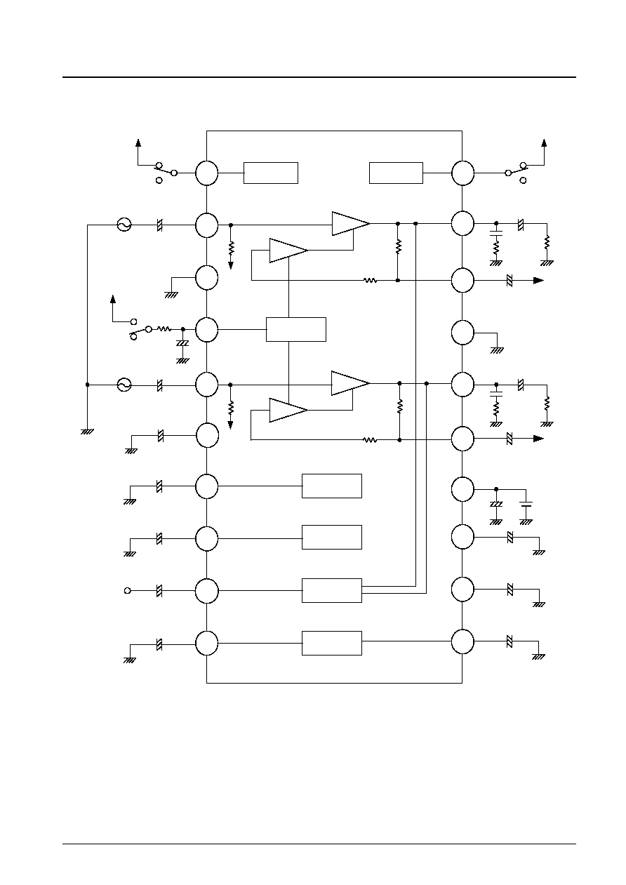
2
4
10
15
13
14
16
18
19
17
12
1
3
5
8
7
9
20
* Package : MSOP-20
Top view
11
PW SW
MT SW
Boost SW
Vref B
Beep
R.F
ON
C1
C2
C4
C5
C6
C7
C8
C12
C13
R2
C14
C15
C16
C18
C17
C11
C10
C9
R1
C3
OFF
OFF
+
+
+
+
+
+
+
0.47
µ
F
0.47
µ
F
+
-
Vcc
22
µ
F
4.7
µ
F
4.7
µ
F
6
+
0.1
µ
F
10
220
µ
F
16
+
0.1
µ
F
10
220
µ
F
16
10k
10k
220
µ
F
+
Vcc
Vcc
Vref A
Vref B
Pre GND
PW SW
IN A
Pre
GND
Boost
SW
IN B
Vref
OUT A
Vref
OUT B
Beep
IN
R.F
OUT
R.F
CONT
Vref
CONT C
L.B C
Vcc
BST NF
B
OUT B
BST NF
A
OUT A
MT SW
PWR
GND
MUTE C
10k
10k
10
µ
F
10
µ
F
+
22
µ
F
+
1
µ
F
+
+
2.2
µ
F
2.2
µ
F
+
0.1
µ
F
Vref A
A
B
ON
+
51k
1
µ
F
ON
OFF
Vcc
Block Diagram and Test Circuit

No. 6657-5/10
LA4802T
External Components (Values in parentheses are recommended values.)
∑ C1, C2 (1 to 10 µF)
Input coupling capacitors.
∑ C3 (0.47 to 2.2 µF)
Boost switch on/off impulse noise reduction capacitor.
∑ C4 (1 µF)
Mute switch on/off impulse noise reduction capacitor.
∑ C5, C6 (10 to 22 µF)
Reference bias (V
REF
) decoupling capacitors.
∑ C7 (0.1 to 1 µF)
Beep input coupling capacitor. Be careful not to attenuate the beep tone signal.
∑ C8, C9 (2.2 to 4.7 µF)
Ripple filter capacitors.
∑ C10 (2.2 to 4.7 µF)
Reference bias (V
REF
) decoupling capacitors.
∑ C11 (1 to 2.2 µF)
Boost switch on/off impulse noise reduction capacitor.
∑ C12 (220 µF)
Power supply line decoupling capacitor.
∑ C13, C16 (0.47 µF)
Low pass filter capacitor in the bass boost circuit. The amount of bass boost depends on the value of this capacitor.
∑ C14, C17 (0.1 µF)
Output oscillation prevention capacitors. We recommend using Mylar capacitors. Since the oscillation stability
varies depending on the PCB layout and other factors, we recommend a value of at least 0.1 µF for these capacitors.
∑ C15, C18 (220 to 470 µF)
Output capacitors. Low band attenuation increases with lower capacitances.
∑ R1 (24 to 51 k
)
Smoothing resistor for the boost switch on/off transition. Note that using a smaller value will increase the idling
current when the boost switch is off.
∑ R2, R3 (10
)
Output oscillation prevention resistors.
No. 6657-6/10
LA4802T
2
4
10
15
13
14
16
18
19
17
12
1
3
5
8
7
9
20
* Package : MSOP-20
11
PW SW
MT SW
Boost SW
Vref B
Beep
R.F
ON
OFF
+
+
+
+
+
+
1
µ
F
+
-
Vcc
22
µ
F
4.7
µ
F
4.7
µ
F
+
0.1
µ
F
10
220
µ
F
16
+
0.1mF
10
220
µ
F
16
10k
10k
220
µ
F
+
Vcc
Vref A
Pre GND
PW SW
IN A
Pre
GND
Boost
SW
IN B
Vref
OUT A
Vref
OUT B
Beep
IN
R.F
OUT
R.F
CONT
Vref
CONT C
L.B C
VCC
BST NF
B
OUT B
BST NF
A
OUT A
MT SW
PWR
GND
MUTE C
10k
10k
10
µ
F
10
µ
F
+
1
µ
F
+
0.1
µ
F
Vref A
A
B
ON
OFF
Vcc
+
2.2
µ
F
+
2.2
µ
F
Top view
6
Application that does not use the line outputs (The bass compensation circuit is always on.)
No. 6657-7/10
LA4802T
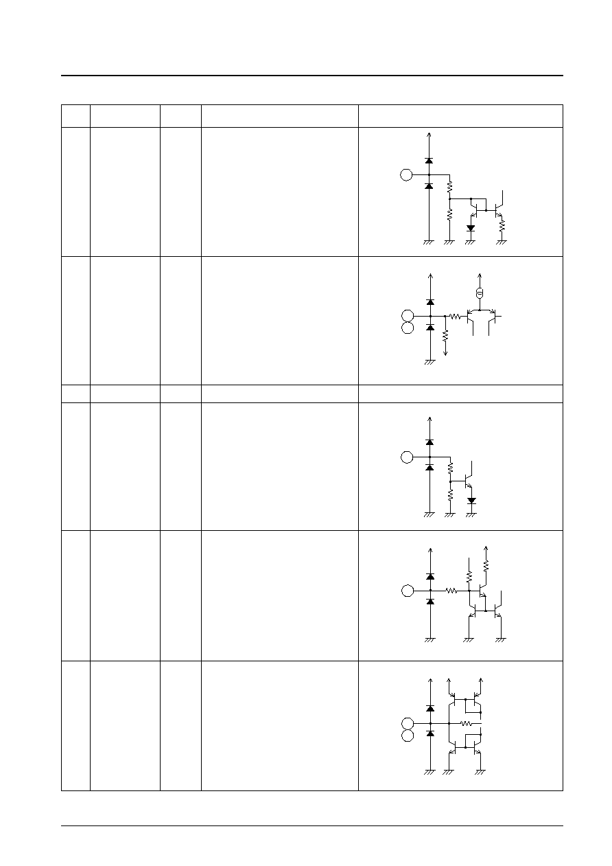
Pin Descriptions
Pin No.
Pin name
Pin
Pin description
Equivalent circuit
voltage (V)
∑ IC on/off switch
∑ 0 to 0.5 V: IC off
∑ 1.4 to 4.5 V: IC on
1
POWER SW
A13730
300k
20k
1
Continued on next page.
∑ Power input
2
5
POWER IN
1.21
A13731
1k
10k
2
5
∑ Bass compensation circuit on/off switch
∑ 0 to 0.5 V: Boost on
∑ 1.4 to 4.5 V: Boost off
4
BOOST SW
A13732
200k
300
4
∑ Connection for the mute switch on/off
impulse noise reduction capacitor
6
MUTE C
1.27
A13733
10k
300
6
3
PRE GND
∑ V
REF
amplifier reference
7
8
V
REF
OUT
1.21
A13734
10k
7
8
No. 6657-8/10
LA4802T
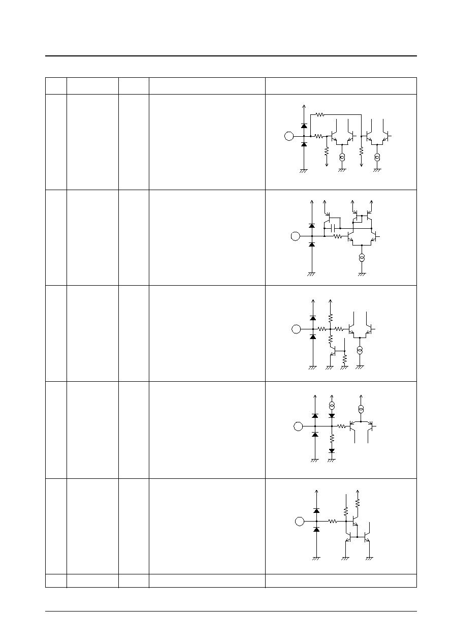
Continued from preceding page.
Pin No.
Pin name
Pin
Pin description
Equivalent circuit
voltage (V)
∑ Beep input
9
BEEP IN
1.21
A13735
2.5k
2.5k
300
300
9
∑ Ripple filter output
10
RF OUT
2.15
A13736
300
10
∑ Ripple filter reference
11
RF CONT
2.15
A13737
100k
45k
12k
300
11
∑ V
REF
amplifier reference
12
V
REF
CONT C
1.21
A13738
10k
13k
12
14
V
CC
∑ Connection for the bass compensation
circuit switch on/off impulse noise
reduction capacitor
13
L. B C
1.33
A13739
300
100k
13
Continued on next page.
No. 6657-9/10
LA4802T
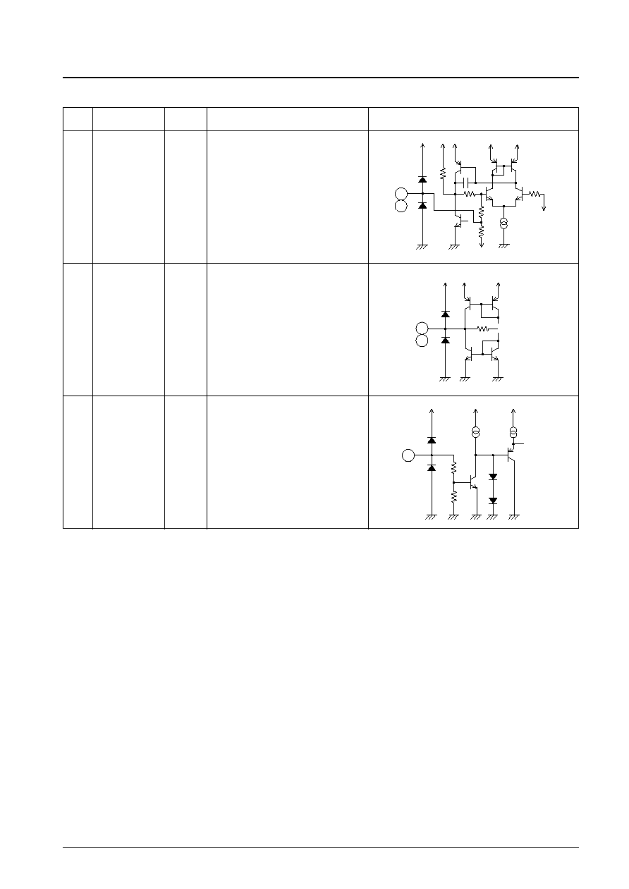
Continued from preceding page.
Pin No.
Pin name
Pin
Pin description
Equivalent circuit
voltage (V)
∑ Bass compensation circuit low-pass filter
connection
∑ The amount of bass boost depends on the
capacitance used.
15
18
L. B NF
1.23
A13740
75k
40k
10k
PWR OUT
PWR NF
15
18
30k
∑ Power outputs
16
19
POWER OUT
1.23
A13741
16
19
15k
∑ Muting on/off switch
∑ 0 to 0.5 V: Muting off
∑ 1.4 to 4.5 V: Muting on
20
MUTE SW
A13742
200k
100k
20
PS No. 6657-10/10
LA4802T
This catalog provides information as of July, 2002. Specifications and information herein are subject to
change without notice.
Specifications of any and all SANYO products described or contained herein stipulate the performance,
characteristics, and functions of the described products in the independent state, and are not guarantees
of the performance, characteristics, and functions of the described products as mounted in the customer's
products or equipment. To verify symptoms and states that cannot be evaluated in an independent device,
the customer should always evaluate and test devices mounted in the customer's products or equipment.
SANYO Electric Co., Ltd. strives to supply high-quality high-reliability products. However, any and all
semiconductor products fail with some probability. It is possible that these probabilistic failures could
give rise to accidents or events that could endanger human lives, that could give rise to smoke or fire,
or that could cause damage to other property. When designing equipment, adopt safety measures so
that these kinds of accidents or events cannot occur. Such measures include but are not limited to protective
circuits and error prevention circuits for safe design, redundant design, and structural design.
In the event that any or all SANYO products (including technical data, services) described or contained
herein are controlled under any of applicable local export control laws and regulations, such products must
not be exported without obtaining the export license from the authorities concerned in accordance with the
above law.
No part of this publication may be reproduced or transmitted in any form or by any means, electronic or
mechanical, including photocopying and recording, or any information storage or retrieval system,
or otherwise, without the prior written permission of SANYO Electric Co., Ltd.
Any and all information described or contained herein are subject to change without notice due to
product/technology improvement, etc. When designing equipment, refer to the "Delivery Specification"
for the SANYO product that you intend to use.
Information (including circuit diagrams and circuit parameters) herein is for example only; it is not
guaranteed for volume production. SANYO believes information herein is accurate and reliable, but
no guarantees are made or implied regarding its use or any infringements of intellectual property rights
or other rights of third parties.