 | –≠–ª–µ–∫—Ç—Ä–æ–Ω–Ω—ã–π –∫–æ–º–ø–æ–Ω–µ–Ω—Ç: LA5318V | –°–∫–∞—á–∞—Ç—å:  PDF PDF  ZIP ZIP |
Overview
The LA5318V is a variable voltage-dividing voltage
generator IC designed for driving LCD matrixes that
require multiple voltages.
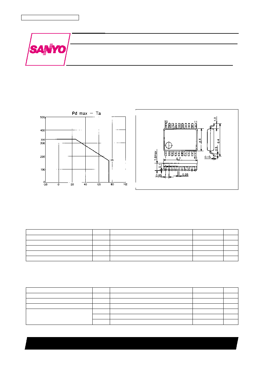
Package Dimensions
unit: mm
3179A-SSOP20
Monolithic Linear IC
Ordering number : EN5670
82097HA(OT) No. 5670-1/4
SANYO: SSOP20
[LA5318V]
SANYO Electric Co.,Ltd. Semiconductor Bussiness Headquarters
TOKYO OFFICE Tokyo Bldg., 1-10, 1 Chome, Ueno, Taito-ku, TOKYO, 110 JAPAN
Voltage-Dividing Voltage Generator
for Multi-Voltage LCD Matrix Drive
LA5318V
Parameter
Symbol
Conditions
Ratings
Unit
Maximum supply voltage
V
EE
max
V
CC
≠ V
EE
36
V
Maximum output current
I
OUT
max
V1 to V4
Internal
*
mA
Allowable power dissipation
Pd max
330
mW
Operating temperature
Topr
≠20 to +75
∞C
Storage temperature
Tstg
≠30 to +125
∞C
Specifications
Absolute Maximum Ratings
at Ta = 25∞C
Parameter
Symbol
Conditions
Ratings
Unit
Supply voltage
V
EE
V
CC
≠ V
EE
≠35.5 to ≠6
V
Input voltage
V
REF
V
CC
≠ V
REF
: V
REF
V
EE
≠35 to ≠6
V
Input current
I
INR
INR
≠0.2 to 0
mA
I
OUTR
OUTR
0 to 50
mA
Output current
I
OUT
1, 2
V1, V2
≠5 to +5
mA
I
OUT
3,4
V3, V4
≠10 to +5
mA
Operating Conditions
at Ta = 25∞C
Notes:
*
The value stipulated in the conditions listed in the separate document shall be used as the maximum output current.
1. Continuous operation (without damage to the device) is guaranteed in the above ranges.
2. The output pins V1 to V4 may be shorted to the power supply or to ground for periods of up to 1 ms. (When |V
CC
≠ V
EE
| < 35 V)
Note: V
CC
and V
EE
must be set up so that |V1| and |V
EE
≠ V4| are at least 1 V.
Allowable power dissipation, Pd ≠ mW
Ambient temperature, Ta ≠
∞
C
No. 5670-2/4
LA5318V
Parameter
Symbol
Conditions
Ratings
Unit
min
typ
max
Current drain
I
CC
, I
EE
V
CC
≠ V
EE
= ≠20 V, R
X
= 8R, INR = V
CC
: V
CC
, V
EE
0.35
0.5
mA
Output voltage ratio 1
Ra1
V2/V1
1.96
2.00
2.04
Output voltage ratio 2
Ra2
(V
REF
≠ V3)/(V
REF
≠ V4)
1.96
2.00
2.04
Output voltage ratio 3
Rb1
V
REF
/V1
11.64
12.00
12.36
Output voltage ratio 4
Rb2
V
REF
/V2
5.82
6.00
6.18
Output voltage ratio 5
Rb3
V
REF
/(V
REF
≠ V3)
5.82
6.00
6.18
Output voltage ratio 3
Rb4
V
REF
/(V
REF
≠ V4)
11.64
12.00
12.36
Internal resistance ratio 1
R
X
1
R
X
1 ≠ R
X
2
8
Internal resistance ratio 2
R
X
2
R
X
1 ≠ R
X
3 Referenced to the resistance
12
Internal resistance ratio 3
R
X
3
R
X
1 ≠ R
X
4 R between R
X
4 and V
IN
3
14
Internal resistance ratio 4
R
X
4
R
X
1 ≠ V
IN
3
15
Resistance
R
The value of R when the voltage across
30
k
R
X
4 and V
IN
3 is 0.5 V.
Load regulation 1
V1
+0.1 mA < I
OUT
1 < +5 mA : V1
±20
mV
Load regulation 2
V2
+0.1 mA < I
OUT
2 < +5 mA : V2
±20
mV
Load regulation 3
V3
+0.1 mA < I
OUT
3 < +5 mA : V3
±20
mV
Load regulation 4
V4
+0.1 mA < I
OUT
4 < +5 mA : V4
±20
mV
Load regulation ≠1A
≠
V1A
≠0.5 mA < I
OUT
1 < ≠0.1 mA : V1
±20
mV
Load regulation ≠2A
≠
V2A
≠0.5 mA < I
OUT
2 < ≠0.1 mA : V2
±20
mV
Load regulation ≠3
≠
V3
≠10 mA < I
OUT
3 < ≠0.1 mA : V3
±20
mV
Load regulation ≠4
≠
V4
≠10 mA < I
OUT
4 < ≠0.1 mA : V4
±20
mV
Load regulation ≠1B
≠
V1B
≠5 mA < I
OUT
1 < ≠0.1 mA, B
IN
= GND : V1
±20
mV
Load regulation ≠2B
≠
V2B
≠5 mA < I
OUT
2 < ≠0.1 mA, B
IN
= GND : V2
±20
mV
OUTR pin saturation voltage
V
OUTR
I
OUT
= 20 mA, V
CC
≠ INR = 2.7 : OUTR ≠ V
EE
0.5
V
Operating Characteristics
at Ta = 25∞C, V
CC
≠V
EE
= ≠20 V, V
REF
= V
EE
, R
X
= 8R, B
IN
= OPEN
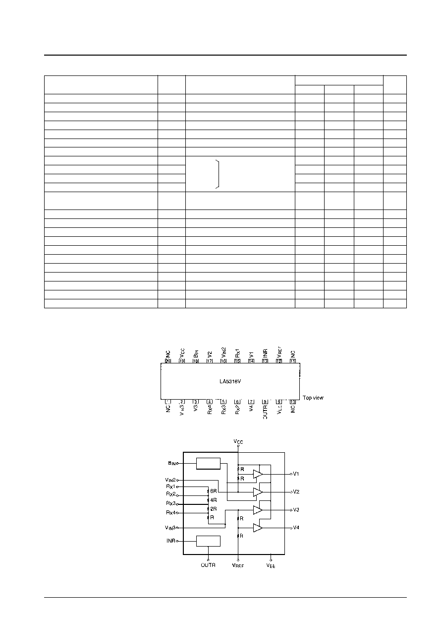
Pin Assignment
Block Diagram
(This circuit must be used with V
RX
1
V
RX
2
V
RX
3
V
RX
4.)
V1, V2 bias
control
V
REF
control
Note: For I
OUT
, minus (≠) indicates source current and plus (+) indicates sink current.
No. 5670-3/4
LA5318V
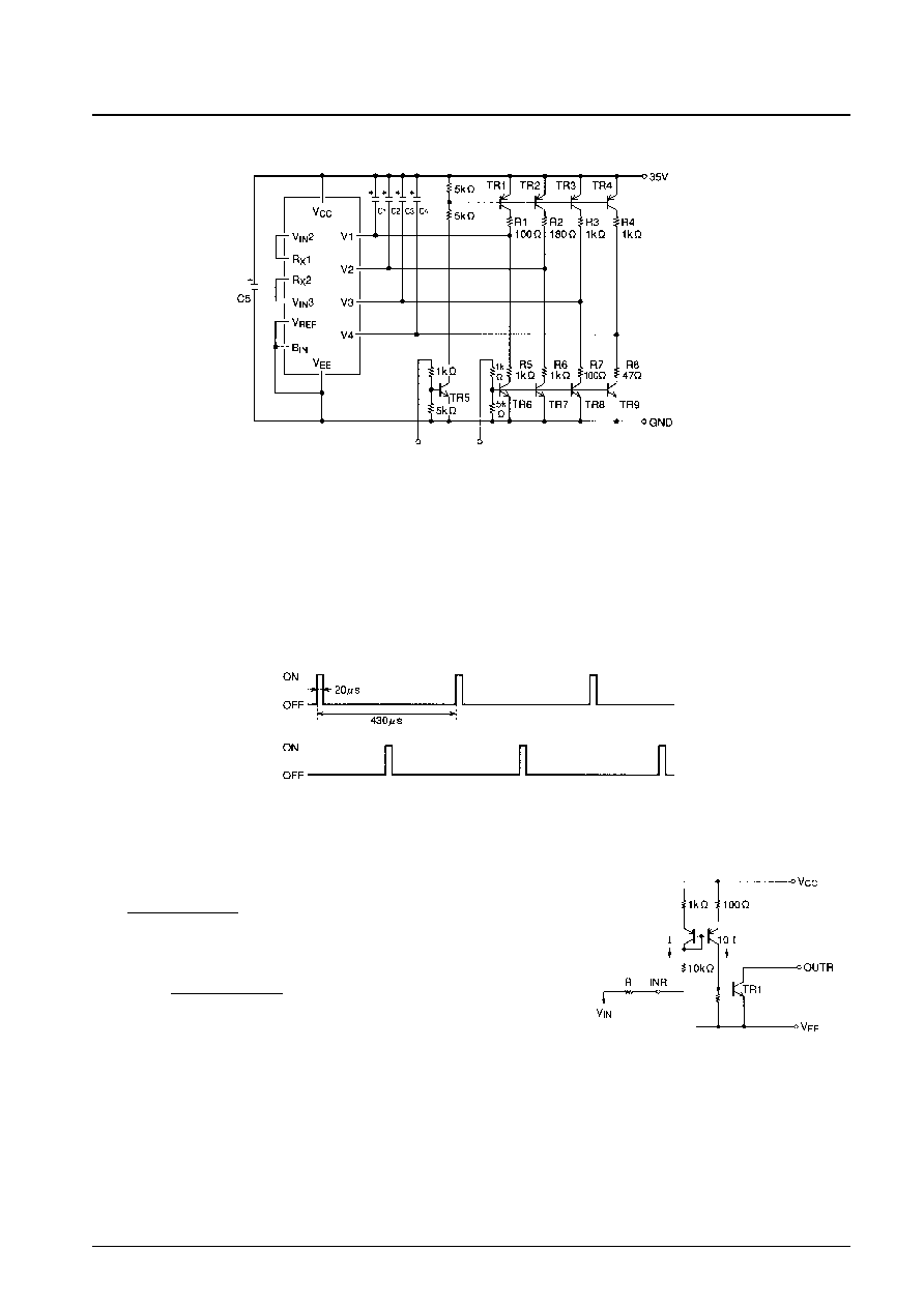
Maximum Output Current Load Test Conditions
V
CC
≠ V
EE
= 35 V, R
X
= 8R, C1 to C4 = 10 µF, C5 = 33 µF, All resistors must be rated 1 W or higher.
TR1 to TR4; 2SA984 Rank E or F
TR5 to TR9; 2SC2274 Rank E or F
Set the output load resistors (R1 to R8) so that currents of 25 to 30 mA maximum (except for the V3 and V4 source
sides, which can handle about 60 mA) flow in the sink and source sides when high (on state) levels are input to inputs 1
and 2.
∑ V
REF
control block
Determining the TR1 drive current
I =
V
CC
≠ V
BE
≠ V
IN
11 k + R
(V
BE
0.7 V)
Drive current
I
O
10I =
V
CC
≠ 0.7 ≠ V
IN
11 k + R
Assume that the TR1
hFE
is 50 for this calculation.
Note: Connect INR to V
CC
when INR and OUTR are not used.
Input 1
Input 1
Input 2
Input 2
◊
10

No. 5670-4/4
LA5318V
This catalog provides information as of August, 1997. Specifications and information herein are subject to
change without notice.
s
No products described or contained herein are intended for use in surgical implants, life-support systems, aerospace
equipment, nuclear power control systems, vehicles, disaster/crime-prevention equipment and the like, the failure of
which may directly or indirectly cause injury, death or property loss.
s
Anyone purchasing any products described or contained herein for an above-mentioned use shall:
Accept full responsibility and indemnify and defend SANYO ELECTRIC CO., LTD., its affiliates, subsidiaries and
distributors and all their officers and employees, jointly and severally, against any and all claims and litigation and all
damages, cost and expenses associated with such use:
Not impose any responsibility for any fault or negligence which may be cited in any such claim or litigation on
SANYO ELECTRIC CO., LTD., its affiliates, subsidiaries and distributors or any of their officers and employees
jointly or severally.
s
Information (including circuit diagrams and circuit parameters) herein is for example only; it is not guaranteed for
volume production. SANYO believes information herein is accurate and reliable, but no guarantees are made or implied
regarding its use or any infringements of intellectual property rights or other rights of third parties.
Current drain, I
CC
≠ mA
Output voltage, V
OUT
≠ V
Output voltage ratio, Rb1, Rb4
Output voltage ratio, Rb2, Rb3
Output voltage ratio, Rb1, Rb2
Output voltage, V
OUT
≠ V
Supply voltage, V
CC
≠ V
Output current, I
OUT
≠ mA
Output Voltage Ratio ≠ Ta
Output current, I
OUT
≠ mA
Ambient temperature, Ta ≠ ∞C
(Sink side)
(Source side)