 | –≠–ª–µ–∫—Ç—Ä–æ–Ω–Ω—ã–π –∫–æ–º–ø–æ–Ω–µ–Ω—Ç: LA5611 | –°–∫–∞—á–∞—Ç—å:  PDF PDF  ZIP ZIP |

Multifunctional Voltage Regulator
for TVs and VCRs
Applications
.
Audiovisual equipment, VCRs and TVs
Features
.
Low saturation type of regulator (ON/OFF function built in)
.
Control amplifier built in.
.
Current limit and thermal limit circuits built in
.
Reverse current prevention provided (V
O
4)
Package Dimensions
unit : mm
3107-SIP13H
[LA5611]
SANYO : SIP13H
Specfications
Maximum Ratings
at Ta = 25 ∞C
Parameter
Symbol
Conditions
Ratings
Unit
Maximum input voltage
V
IN
1 max
22
V
V
IN
2 max
V
IN
1
^
V
IN
2
V
IN
1
Allowable power dissipation
Pd max
No heat sink
2
W
Thermal resistance between
junction and case
j-c
4.7
∞C/W
Operating temperature
Topr
≠20 to +80
∞C
Storage temperature
Tstg
≠40 to +150
∞C
Operating Conditions
at Ta = 25 ∞C
Parameter
Symbol
Conditions
Ratings
Unit
Input voltage
V
IN
1
11.5 to 20
V
V
IN
2
6.2 to 20
V
Output current 1
I
O
1
Within ASO of external Tr
mA
Output current 2
I
O
2
10 to 480
mA
Output current 3
I
O
3
10 to 240
mA
Output current 4
I
O
4
5 to 48
mA
Ordering number: EN 5196
Monolithic Linear IC
LA5611
SANYO Electric Co.,Ltd. Semiconductor Bussiness Headquarters
TOKYO OFFICE Tokyo Bldg., 1-10, 1 Chome, Ueno, Taito-ku, TOKYO, 110 JAPAN
92895HA (II) No.5196-1/5
Operating Characteristics
at Ta = 25 ∞C, See specified Test Circuit.
Parameter
Symbol
Conditions
min
typ
max
Unit
[No-load mode] V
EN
= low, V
IN
1 = 14 V, V
IN
2 = 6.6 V, I
O
1 to I
O
4 = 0 mA
Quiescent current
I
IN
1
8
16
mA
I
IN
2
2
4
mA
[Regulator 1] V
EN
= low, V
IN
1 = 14 V, V
IN
2 = 6.6 V, I
O
1 = 500 mA, with specified extenal transistor
Output voltage 1
V
O
1
8.5
9.0
9.5
V
Dropout voltage
V
DROP
1
0.8
1.6
V
Line regulation
n
V
OLN
1
12 V
%
V
IN
1
%
16 V
140
mV
Load regulation
n
V
OLD
1
0.1 A
%
I
O
1
%
1 A
150
mV
Ripple rejection
Rrej1
50
dB
Output low-level voltage
V
O
1 OFF
0.2
V
Control output current
I
CONT
1
10
mA
Output voltage/temperature
coefficient
n
V
O
1/
n
Ta
±
1
mV/ ∞C
[Regulator 2] V
EN
= low, V
IN
1 = 14 V, V
IN
2 = 6.6 V, I
O
2 = 400 mA
Output voltage 2
V
O
2
4.80
5.05
5.30
V
Dropout voltage
V
DROP
2
0.5
1.0
V
Line regulation
n
V
OLN
2
6 V
%
V
IN
2
%
7.2 V
20
mV
Load regulation
n
V
OLD
2
0.1 A
%
I
O
2
%
0.4 A
100
mV
Peak output current
I
OP
2
480
mA
Output short-circuit current
I
OSC
2
90
240
mA
Ripple rejection
Rrej2
50
dB
Output low-level voltage
V
O
2 OFF
0.2
V
Output voltage/temperature
coefficient
n
V
O
2/
n
Ta
±
0.5
mV/ ∞C
[Regulator 3] V
EN
= high, V
IN
1 = 14 V, V
IN
2 = 6.6 V, I
O
3 = 200 mA
Output voltage 3
V
O
3
4.80
5.05
5.30
V
Dropout voltage
V
DROP
3
0.5
1.0
V
Line regulation
n
V
OLN
3
6 V
%
V
IN
2
%
7.2 V
20
mV
Load regulation
n
V
OLD
3
10 mA
%
I
O
3
%
200 mA
100
mV
Peak output current
I
OP
3
240
mA
Output short-circuit current
I
OSC
3
40
120
mA
Ripple rejection
Rrej3
50
dB
Output voltage/temperature
coefficient
n
V
O
3/
n
Ta
±
0.5
mV/ ∞C
[Regulator 4] V
EN
= high, V
IN
1 = 14 V, V
IN
2 = 6.6 V, I
O
4 = 40 mA
Output voltage 4
V
O
4
5.4
5.7
6.0
V
Dropout voltage
V
DROP
4
3.8
5.0
V
Line regulation
n
V
OLN
4
12 V
%
V
IN
1
%
16 V
40
mV
Load regulation
n
V
OLD
4
10 mA
%
I
O
4
%
40 mA
65
mV
Peak output current
I
OP
4
40
mA
Output short-circuit current
I
OSC
4
70
mA
Ripple rejection
Rrej4
50
dB
Output voltage/temperature
coefficient
n
V
O
4/
n
Ta
±
1
mV/ ∞C
[Output on/off control] V
IN
1 = 14 V, V
IN
2 = 6.6 V
Output on control voltage
V
ENL
V
O
1, V
O
2: on
1.0
V
Output off control voltage
V
ENH
V
O
1, V
O
2: off
3.0
V
IN
1
V
[Control Amplifier] V
IN
1 = 14 V, V
IN
2 = 6.6 V
Control output current
I
CONT
2
10
mA
Resistance ratio
K
R
K
R
= R4/R3, Vref = 1.28 V typ
9.94
LA5611
No.5196 - 2/5
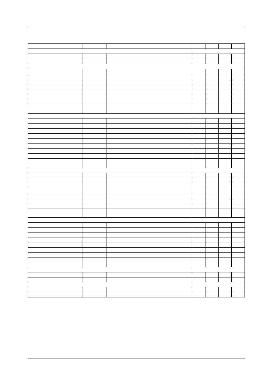
Note 1: The tightening torque referred to in the above figure is a condition specified for the heat dissipation characteristics and not
a working condition to be met when mounting the heat sink.
Test Circuit
or
its equivalent
Phase
compensation
Pin Functions
No.
Symbol
Function
1
V
O
3
5.05 V/240 mA regulator, with current limit, thermal shutdown.
2
EN
Regulator 1 and regulator 2 on/off control. Low active.
3
GND
Substrate of the LA5611 (minimum potential).
4
V
O
2
5.05 V/480 mA regulator, with on/off, current limit, thermal shutdown.
5
V
IN
2
Low voltage input.
6
V
O
4
5.7 V/40 mA regulator with reverse current prevention.
7
ADJ2
V
O
1 adjustment pin. Resistance between pin 7 and ground
V
O
1 up.
Resistance between pin 7 and pin 8
V
O
1 down
8
V
O
1
Output voltage sensor of 9.0 V regulator
9
CONT1
Base control of external NPN transistor. I
CONT
1 = 10 mA, with on/off, thermal shutdown coupled with
the internal thermal shutdown of this regulator.
10
ADJ1
V
IN
1 adjustment pin. Resistance between pin 10 and ground
V
IN
1 up.
Resistance between pin 13 and pin 10
V
IN
1 down
11
PC
Phase correction pin of switching regulator control amplifier.
12
CONT2
Drive output of switching regulator control amplifier.
13
V
IN
1
High voltage input.
Aluminum heat sink
mounting conditions
Tightening torque: 4 kg
.
cm Note 1
With plain washer and
silicone grease applied
Infinite heat sink
Allowable
power
dissipation,
Pd
max
--
W
Ambient temperature, Ta -- ∞C
No heat sink
Pd max -- Ta
LA5611
No.5196 - 3/5
Function Table
(
V
: built in,
◊
: not built in)
Circuit block
Function
V
O
1
V
O
2
V
O
3
V
O
4
Control
amplifier
Input line
V
IN
1
V
IN
2
V
IN
2
V
IN
1
V
IN
1
Current limit
◊
V
V
V
◊
Thermal limit
V
V
V
◊
◊
On/off control
V
V
◊
◊
◊
Usage Notes
(1) Apply voltages to the voltage input pins on condition that V
IN
1
^ V
IN
2.
(2) Supply the voltages simultaneously to V
IN
1 and V
IN
2. Do not use the LA5611 with voltage applied to only one of these pins.
(3) Since the control circuit of regulator 1 does not have current limit protection of such as an external NPN transistor, provide
this protection in each application.
Logic Table
Conditions : when V
IN
1
^ V
IN
2 (at V
IN
1
^ 11.5 V, V
IN
2
^ 6.2 V)
EN
V
O
1, V
O
2
L or open
H
H
L
(1) ``H'' for EN denotes high level; ``L'' denotes low level.
(2) ``H'' for V
O
denotes output ON voltage; ``L'' denotes output OFF voltage.
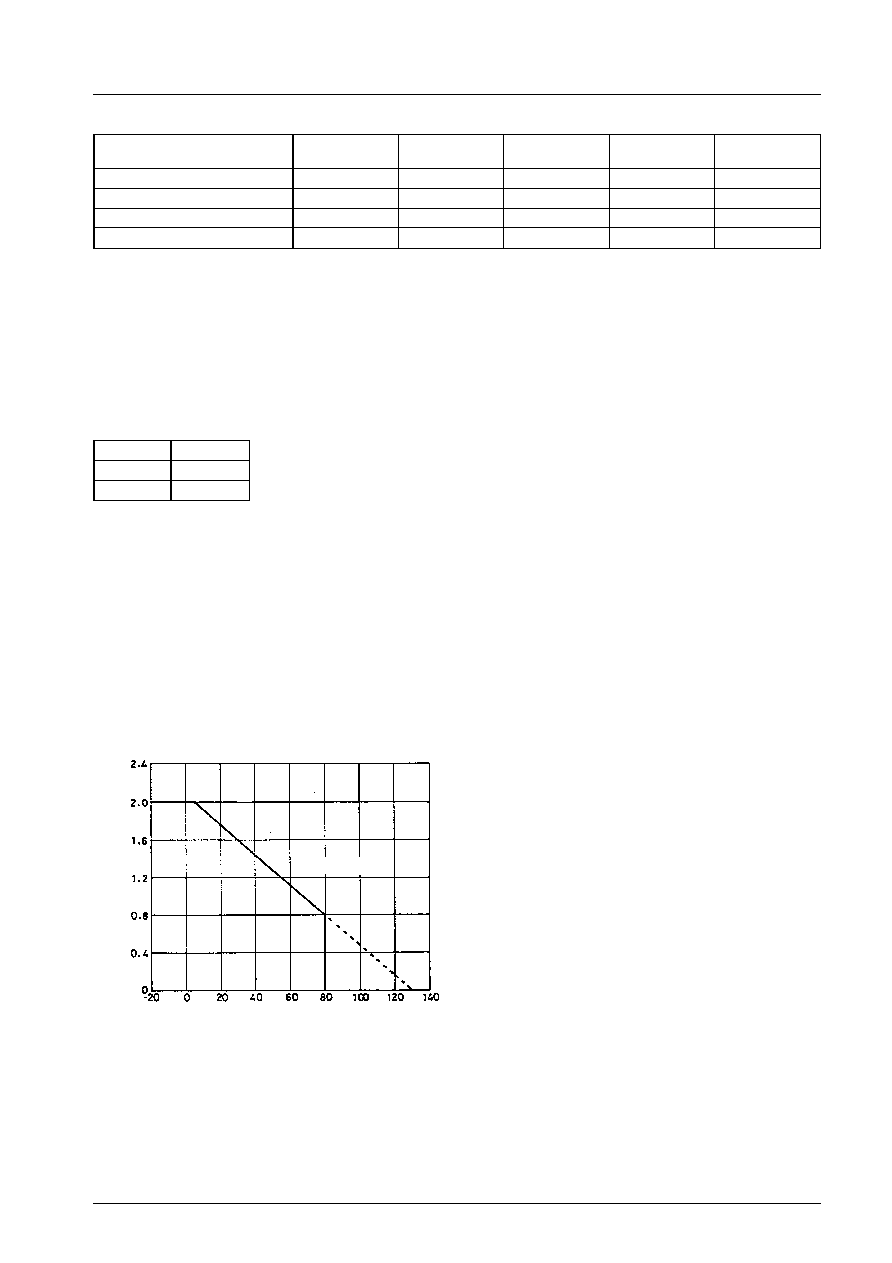
Thermal Design Notes
(1) In the LA5611, the junction temperature (Tj) at which thermal shutdown is activated is approximately equal to 130∞C.
(2) Consequently, the operating temperature range of REG1, REG2 and REG3 with the thermal shutdown function is restricted
by the thermal shutdown characteristics (typical value) shown in the figure below.
(3) The thermal shutdown characteristics vary ±20∞C or so. Since thermal shutdown is liable to occur with inadequate heat
dissipation, sufficient consideration must be given to the heat dissipation design.
Thermal Shutdown Characteristics
Typical Characteristics
Allowable
power
dissipation,
Pd
--
W
Ambient temperature, Ta -- ∞C
LA5611
No.5196 - 4/5
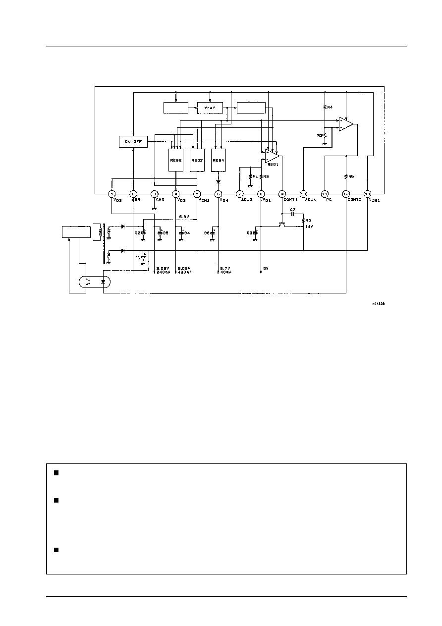
Equivalent Circuit Block Diagram and Sample Application Circuit
Application Notes
(1) Depending on the type, load current and connection position (distance from the LA5611) of the external NPN transistor, the
capacitor C7 and resistance R6 is necessary for preventing oscillation.
(2) C1 to C6 are bypass capacitors for preventing oscillation: as such, they must be positioned as close to the LA5611 as possible
in order to stabilize operation.
No products described or contained herein are intended for use in surgical implants, life-support systems, aerospace equipment,
nuclear power control systems, vehicles, disaster/crime-prevention equipment and the like, the failure of which may directly or
indirectly cause injury, death or property loss.
Anyone purchasing any products described or contained herein for an above-mentioned use shall:
1
Accept full responsibility and indemnify and defend SANYO ELECTRIC CO., LTD., its affiliates, subsidiaries and distributors
and all their officers and employees, jointly and severally, against any and all claims and litigation and all damages, cost and
expenses associated with such use:
2
Not impose any responsibility for any fault or negligence which may be cited in any such claim or litigation on SANYO
ELECTRIC CO., LTD., its affiliates, subsidiaries and distributors or any of their officers and employees jointly or severally.
Information (including circuit diagrams and circuit parameters) herein is for example only; it is not guaranteed for volume
production. SANYO believes information herein is accurate and reliable, but no guarantees are made or implied regarding its use
or any infringements of intellectual property rights or other rights of third parties.
This catalog provides information as of September, 1995. Specifications and information herein are subject to change without notice.
Start-up
Thermal
Shutdown
detection
Converter transformer
Reverse
current
prevention
External Tr
Phase
compensation
Switching
regulator
control
amplifier
Photocoupler
Error
amplifier
Switching
regulator
LA5611
No.5196 - 5/5