 | –≠–ª–µ–∫—Ç—Ä–æ–Ω–Ω—ã–π –∫–æ–º–ø–æ–Ω–µ–Ω—Ç: LA5621V | –°–∫–∞—á–∞—Ç—å:  PDF PDF  ZIP ZIP |
Ordering number :EN5640A
31000RM (OT) No. 5640-1/6
Overview
The LA5621M and LA5621V are external charge control
ICs for lithium-ion batteries. These ICs are ideally suited
for on/off control of external power MOSFETs in systems
that incorporate a charging circuit in the set. They detect
the charge and discharge status, output it to the set control
microcontroller, which then outputs a signal to switch
external power MOSFETS either on or off. Moreover,
these ICs have a built-in function that detects discharge
(countercurrent) from lithium-ion batteries within sets to
external lithium-ion batteries in an AC adapter/charger,
etc. and switches external power MOSFETs off.
Application
∑ Charge control of 1- or 2-cell lithium-ion batteries of
video cameras, digital still cameras, cellular telephones,
etc., used in combination with a microcontroller.
Functions
∑ Charge/discharge: In charge/discharge mode, switch
external power MOSFETs on to charge the battery or
discharge it to set load.
∑ Charge detection: Detect the charge status of lithium-ion
batteries with comparator.
∑ Charge completion control: When charging of the
lithium-ion battery is completed, the comparator is
activated and the external power MOSFETs are
switched off to stop charging.
∑ Countercurrent detection and control:
In systems that support charging of both the set of the
video camera, etc., and the AC adapter/charger, when
spare batteries are charged on the AC adapter/charger
side, if the battery voltage on the set side becomes high
when the set is connected to the AC adapter/charger,
current flows out to the battery on the AC
adapter/charger side. These ICs feature a function that
prevents this from happening.
∑ Charge prevention: A specified voltage is applied to the
CHARGEINH pin to stop charging.
Features
∑ The combination of a microcontroller and external
power MOSFETs enables easy charge/discharge control
of lithium-ion batteries.
∑ Small power dissipation makes these ICs suitable for
sets that require long time operation
∑ Use of compact package makes these ICs suitable for
compact sets.
∑ Large power supply operation range supports both 1-cell
and 2-cell lithium-ion batteries.
LA5621M, 5621V
SANYO Electric Co.,Ltd. Semiconductor Company
TOKYO OFFICE Tokyo Bldg., 1-10, 1 Chome, Ueno, Taito-ku, TOKYO, 110-8534 JAPAN
Lithium-Ion Battery Charge Control IC
Monolithic linear IC
Any and all SANYO products described or contained herein do not have specifications that can handle
applications that require extremely high levels of reliability, such as life-support systems, aircraft's
control systems, or other applications whose failure can be reasonably expected to result in serious
physical and/or material damage. Consult with your SANYO representative nearest you before using
any SANYO products described or contained herein in such applications.
SANYO assumes no responsibility for equipment failures that result from using products at values that
exceed, even momentarily, rated values (such as maximum ratings, operating condition ranges, or other
parameters) listed in products specifications of any and all SANYO products described or contained
herein.
No. 5640-2/6
LA5621M, 5621V
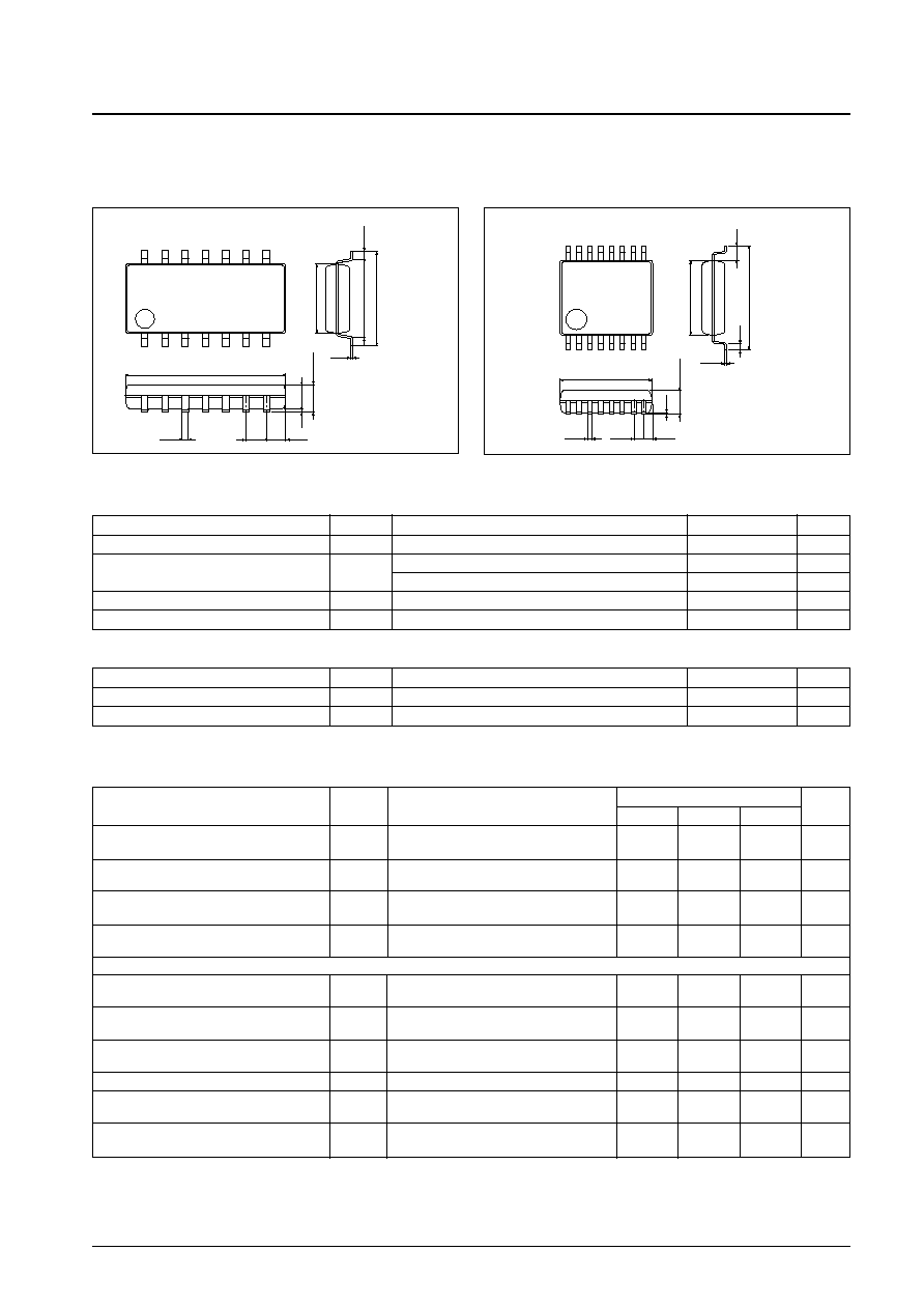
Package Dimensions
unit: mm
3034A-MFP14
unit: mm
3178-SSOP16
1
14
7
8
1.24
1.27
0.35
0.15
10.1
1.8max
1.5
0.1
4.4
5.15
6.4
0.625
[LA5621M]
1
8
9
16
6.4
0.5
4.4
5.4
0.1
1.6max
1.0
0.65
0.22
0.43
0.15
SANYO: SSOP16
[LA5621V]
SANYO: MFP14
Parameter
Symbol
Conditions
Ratings
Unit
Maximum supply voltage
V
CC
max
11
V
Allowable power dissipation
Pd max
LA5621M
320
mW
LA5621V
250
mW
Operating temperature
Topr
≠20 to +75
∞C
Storage temperature
Tstg
≠55 to +125
∞C
Specifications
Maximum Rating
at Ta = 25∞C
Parameter
Symbol
Conditions
Ratings
Unit
Supply voltage 1
V
CC
1
V
CC
1
V
CC
2
1 to 11
V
Supply voltage 2
V
CC
2
V
CC
1
V
CC
2
*
2 to 5.5
V
Allowable Operating Conditions
at Ta = 25∞C
Note:
*
When V
CC
1 < 2 V, only the gate block (external power MOSFET drive) operates.
Parameter
Symbol
Conditions
Ratings
Unit
min
typ
max
Current drain 1-1
I
CC
1-1
V
CC
1 in current, V
CHG
= V
CC
2,
90
120
µA
(During set operation discharge)
SW4, 6: on, SW5: off
Current drain 2-1
I
CC
2-1
V
CC
2 in current, V
CHG
= V
CC
2,
20
26
µA
(During set operation discharge)
SW4, 6: on, SW5: off
Current drain 1-2
I
CC
1-2
V
CC
2 in current, V
CHG
= V
CC
2,
20
26
µA
(During charging outside set)
SW4, 5: on
Current drain 2-2
I
CC
2-2
V
CC
2 in current
600
800
µA
(During charging)
SW5: on, V
CPU
: L, V
GATE
:H
[Output pin block]
High-level CPU pin
V
CPU-H
V
IN
1
≠
= 15 mV, V
IN
1
+
= 11 mV,
V
CC
2 ≠ 0.15
V
V
CHG
= V
CC
2, SW4: off, SW5: on
Low-level CPU pin
V
CPU-L
V
IN
1
≠
= 15 mV, V
IN
1
+
= 23 mV,
0.2
V
V
CHG
= V
CC
2, SW4: off, SW5: on
CPU pin sink current
V
CPU-SINK
V
IN
1
≠
= 15 mV, V
IN
1
+
= 23 mV,
35
µA
V
CHG
= V
CC
2, SW4: off, SW5: on
High-level BIAS1 pin
V
BIAS
1-H
SW1, 2, 5, 6: on
V
CC
2 ≠ 0.15
V
High-level BIAS2 pin
V
BIAS
2-H
SW1, 2, 5, 6: on, V
IN
2
-
= 15 mV,
V
IN
2
+
= 11 mV
V
CC
2 ≠ 0.15
V
Low-level BIAS2 pin leak current
I
BIAS
2-LK
SW1, 2, 5, 6: on,
10
µA
V
IN
1
≠
= 15 mV, V
IN
1
+
= 23 mV
Electrical Characteristics
at Ta = 25∞C, V
CC
1 = 5.5 V, V
CC
2 = 3.15 V (unless otherwise specified)
Continued on next page.
No. 5640-3/6
LA5621M, 5621V
Parameter
Symbol
Conditions
Ratings
Unit
min
typ
max
[FET drive block]
Drive high-level voltage
V
GATE-H
Same as current drain 1-1
5.3
5.4
V
Drive low-level voltage
V
GATE-L
SW6: on, Same as current drain 1-2
0.1
0.2
V
[Comparator block] SW1, 2, 5, 6: on
Input offset voltage 1
V
IO
1
Comparator 1, when CPU voltage is reversed
≠3
+2
+7
mV
Input offset voltage 2
V
IO
2
Comparator 2, when BIAS2 voltage is reversed
≠3
≠1
+1
mV
Input offset voltage 3
V
IO
3
Total temperature, comparator 2
≠5
+3
mV
Input offset current
I
IO
Comparators 1, 2
5
50
nA
Input bias current
I
IB
Comparators 1, 2
≠250
≠25
nA
In-phase input voltage range
V
ICR
Comparators 1, 2
V
CC
2 ≠ 1.5
V
Input current during negative voltage application
I
LIM
Comparators 1, 2 non-reversed input block only, SW3: on
≠1.5
mA
[Input pin block] V
IN
1
≠
= 15 mV, V
IN
1
+
= 23 mV, V
IN
2
≠
= 15 mV, V
IN
2
+
= 23 mV
CHARGE pin threshold voltage
V
CHG-TH
SW1, 2, 5, 6: When on, BIAS2 voltages are reversed
0.5
1.2
V
CHARGE pin input bias current 1
I
CHG-BI
1
Current during threshold voltage
10
µA
CHARGE pin input bias current 2
I
CHG-BI
2
V
CHARGE
= V
CC
2
55
70
85
µA
CHARGE-INH pin open voltage
V
CH-IN-OP
SW1, 2, 5, 6: on
V
CC
2
V
CHARGE-INH pin threshold voltage
V
CH-IN-TH
SW1, 2, 5, 6: When on, BIAS2 voltages are reversed
0.7
1.3
V
CHARGE-INH pin low-level input current
I
CH-IN
SW1, 2, 5, 6: on
≠30
µA
BATT/EXT pin open voltage
V
BA/EX-OP
SW1, 2, 6: on
V
CC
2
V
BATT/EXT pin threshold voltage
V
BA/EX-TH
SW1, 2, 6: When on, BIAS2 voltages are reversed
1.45
2.05
V
BATT/EXT pin low-level input current
V
BA/EX
SW1, 2, 5, 6: on
≠30
µA
Continued from preceding page.
Handling Cautions
Observe precautions when handling these ICs because they are electrostatic sensitive devices.
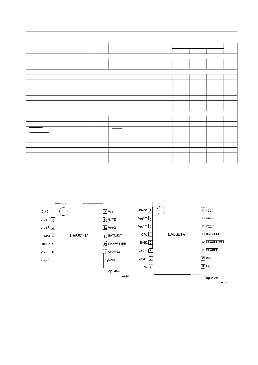
Pin Assignment

Pin Functions
No. 5640-4/6
LA5621M, 5621V
Pin No.
Pin name
Function
LA5621M
LA5621V
1
1
BIAS1
Resistor connection pin for setting non-reversed input potential of comparator 1
2
2
V
IN
1
≠
*
Reversed input of comparator 1 (for charge current detection)
3
3
V
IN
1
+
*
Non-reversed input of comparator 1 (for charge current detection)
4
4
CPU
Microcontroller signal input pin
5
5
BIAS2
Resistor connection pin for setting non-reversed input potential of comparator 2
6
6
V
IN
2
≠
*
Reversed input of comparator 2 (for countercurrent detection when 2 batteries are used)
7
7
V
IN
2
+
*
Non-reversed input of comparator 2 (for countercurrent detection when 2 batteries are used)
--
8
NC
No connection
--
9
NC
No connection
8
10
GND
Substrate of this IC (Lowest potential)
9
11
CHARGE
Charging signal input pin, charge with low
10
12
CHARGE INH
Charge prohibition signal input pin, charge prohibition with low (becomes low during discharge mode
for lithium-ion battery that set operates on)
11
13
BATT/EXT
On/off control pin of this IC, except Gate block (becomes "Open" during discharge mode for
lithium-ion battery that set operates on)
12
14
V
CC
2
Power supply input
13
15
GATE
Gate connection pin of external power MOSFETs
14
16
V
CC
1
Lithium-ion battery + side input pin
Specified Test Circuit
Note:
*
If negative voltage is applied due to countercurrent, etc., up to 1.5 mA can be allowed.
Allowable power dissipation, Pd max -- W
Operating temperature, Ta -- ∞C

Equivalent Circuit Block and Sample Peripheral Circuit
No. 5640-5/6
LA5621M, 5621V
Charge
detection
Countercurrent
detection
Charging/
Discharge
mode
Secondary
lithium-ion
battery
Discharge current
Charge current
FW201 or FW203
equivalent
Load
Set, internal side
Clock, timer, CPU,
backup
Plug/SW
External
wire bound
(ON when plug
is inserted)
(OFF when plug
is inserted)
Secondary
lithium-ion
battery
External
charge adapter
Power
supply for
charging
∑
Charging following internal battery use V
BAT
2 < < V
BAT
1
Normal charging
∑
Full charging on set side; Discharge on adapter side
V
BAT
2 > V
BAT
1
Countercurrent from set to adapter
∑
Discharge/During set use, power MOSFETs are simply switched ON.
Application Cautions:
The charging conditions of the secondary battery to be used must be set according to the battery specifications.
The peripheral circuit constants must be set taking into consideration the specifications of the power MOSFETs.
Microcontroller use conditions must be carefully studied.