 | –≠–ª–µ–∫—Ç—Ä–æ–Ω–Ω—ã–π –∫–æ–º–ø–æ–Ω–µ–Ω—Ç: LA5633 | –°–∫–∞—á–∞—Ç—å:  PDF PDF  ZIP ZIP |
Ordering number : ENN5969A
D2001TN (OT)/O3098RM (OT) No. 5969-1/7
Overview
The LA5633 is a low-saturation regulator IC designed for
use in satellite broadcast tuners (such as tuners for the
Japanese BS and CS systems) and provides four
controllable outputs.
Applications
∑ Power supply systems in BS/CS tuners
∑ Audio Video (AV) equipment that includes any type of
satellite broadcast tuner
∑ Miniature electronic equipment
Functions
∑ Built-in four regulators of low-saturation output
(15.7 V/350 mA, 9 V/250 mA, 12 V/100 mA,
5 V/650 mA)
∑ Output on/off control (active low)
∑ On-chip thermal protection and overcurrent protection
circuits
Features
∑ Provides all four voltages required by BS/CS tuners, and
thus can contribute to end product miniaturization.
∑ V
O
1 can be controlled independently, and V
O
2, V
O
3,
and V
O
4 are controlled together, thus providing a high
degree of flexibility in system design.
∑ The adoption of a low-saturation regulator circuit
reduces internal power dissipation.
∑ Provides 3 inputs to make both low-power design and
thermal design easy.
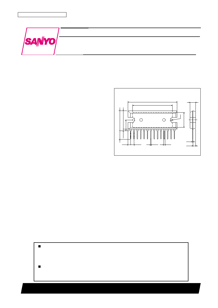
Package Dimensions
unit: mm
3023A-SIP14H
14
1
13.8
0.6
37.0
30.0
R1.7
11.0
8.0
0.8min
6.0
15.0max
1.99
2.54
1.4
0.4
4.5
2.25
SANYO: SIP14H
[LA5633]
LA5633
SANYO Electric Co.,Ltd. Semiconductor Company
TOKYO OFFICE Tokyo Bldg., 1-10, 1 Chome, Ueno, Taito-ku, TOKYO, 110-8534 JAPAN
Satellite Broadcast (BS/CS) Tuner Regulator IC
Monolithic Linear IC
Any and all SANYO products described or contained herein do not have specifications that can handle
applications that require extremely high levels of reliability, such as life-support systems, aircraft's
control systems, or other applications whose failure can be reasonably expected to result in serious
physical and/or material damage. Consult with your SANYO representative nearest you before using
any SANYO products described or contained herein in such applications.
SANYO assumes no responsibility for equipment failures that result from using products at values that
exceed, even momentarily, rated values (such as maximum ratings, operating condition ranges, or other
parameters) listed in products specifications of any and all SANYO products described or contained
herein.

No. 5969-2/7
LA5633
Parameter
Symbol
Conditions
Ratings
Unit
Input voltage
V
IN
max
V
IN
1
V
IN
2
V
IN
3
35
V
Enable pin voltage
V
EN
max
EN1, EN2
V
IN
max
V
Allowable power dissipation
Pd max
With an arbitrarily large heat sink
15
W
With no heat sink
4.3
W
Junction to case thermal resistance
j-c
3
∞C/W
Junction to atmosphere thermal resistance
j-a
29.07
∞C/W
Operating temperature
Topr
≠20 to +80
∞C
Storage temperature
Tstg
≠55 to +150
∞C
Junction temperature
Tj max
150
∞C
Specifications
Maximum Ratings
at Ta = 25∞C
Parameter
Symbol
Conditions
Ratings
Unit
I
O
1
Regulator 1
5 to 350
mA
Output current
I
O
2
Regulator 2
1 to 250
mA
I
O
3
Regulator 3
1 to 100
mA
I
O
4
Regulator 4
5 to 650
mA
Operating Conditions
at Ta = 25∞C
Parameter
Symbol
Conditions
Ratings
Unit
min
typ
max
Regulator 1 [V
EN
1 = low, V
O
1: on, V
IN
1 = 20 V, I
O
1 = 350 mA]
Output voltage 1
V
O
1
14.9
15.7
16.5
V
Dropout voltage
V
DROP
1-1
0.3
0.5
V
V
DROP
1-2 I
O
1 = 175 mA
0.15
0.3
V
Line regulation
V
OLN
1
17.5 V
V
IN
1
23 V
20
100
mV
Load regulation
V
OLD
1
5 mA
I
O
1
350 mA
40
200
mV
Peak output current
I
OP
1
350
540
mA
Output short-circuit current
I
OSC
1
150
mA
Output on control voltage
V
ENL
1
V
O
1 : ON
1.0
V
Output off control voltage
V
ENH
1
V
O
1 : OFF
4.0
V
IN
1
V
Output low-level voltage
V
O
1 OFF
0.2
V
Output noise voltage
V
NOISE
1
10 Hz
f
100 kHz
110
µVrms
Ripple rejection
Rrej1
f = 120 Hz, 18 V
V
IN
1
23 V
50
dB
Regulator 2 [V
EN
2 = low, V
O
2: on, V
IN
2 = 11 V, I
O
2 = 250 mA]
Output voltage 2
V
O
2
8.55
9.0
9.45
V
Dropout voltage
V
DROP
2
0.3
0.5
V
Line regulation
V
OLN
2
10.45 V
V
IN
2
23 V
20
100
mV
Load regulation
V
OLD
2
1 mA
I
O
2
250 mA
30
100
mV
Peak output current
I
OP
2
250
270
mA
Output short-circuit current
I
OSC
2
70
mA
Output on control voltage
V
ENL
2
V
O
2 : ON
1.0
V
Output off control voltage
V
ENH
2
V
O
2 : OFF
4.0
V
IN
2
V
Output low-level voltage
V
O
2 OFF
0.2
V
Output noise voltage
V
NOISE
2
10 Hz
f
100 kHz
110
µVrms
Ripple rejection
Rrej2
f = 120 Hz, 11 V
V
IN
2
23 V
50
dB
Regulator 3 [V
EN
2 = low, V
O
3 on, V
IN
1 = 20 V, I
O
3 = 100 mA]
Output voltage 3
V
O
3
11.4
12.0
12.6
V
Dropout voltage
V
DROP
3
0.3
0.5
V
Line regulation
V
OLN
3
13.6 V
V
IN
1
23 V
20
100
mV
Load regulation
V
OLD
3
1 mA
I
O
3
100 mA
20
50
mV
Peak output current
I
OP
3
100
150
mA
Output short-circuit current
I
OSC
3
40
mA
Output on control voltage
V
ENL
2
V
O
3 : ON
1.0
V
Operating Characteristics
at Ta = 25∞C in the stipulated test circuit
Continued on next page.
No. 5969-3/7
LA5633
Continued from preceding page.
Parameter
Symbol
Conditions
Ratings
Unit
min
typ
max
Output off control voltage
V
ENH
2
V
O
3 : OFF
4.0
V
IN
1
V
Output low-level voltage
V
O
3 OFF
0.2
V
Output noise voltage
V
NOISE
3
10 Hz
f
100 kHz
70
µVrms
Ripple rejection
Rrej3
f = 120 Hz, 14 V
V
IN
1
23 V
55
dB
Regulator 4 [V
EN
2 = low, V
O
4: on, V
IN
3 = 7.0 V, I
O
4 = 650 mA]
Output voltage 4
V
O
4
4.75
5.0
5.25
V
Dropout voltage
V
DROP
4-1
0.3
0.5
V
V
DROP
4-2 I
O
1 = 325 mA
0.2
0.4
V
Line regulation
V
OLN
4
6.25 V
V
IN
3
23 V
20
100
mV
Load regulation
V
OLD
4
5 mA
I
O
4
650 mA
40
200
mV
Peak output current
I
OP
4
650
900
mA
Output short-circuit current
I
OSC
4
250
mA
Output on control voltage
V
ENL
2
V
O
4 : ON
1.0
V
Output off control voltage
V
ENH
2
V
O
4 : OFF
4.0
V
IN
3
V
Output low-level voltage
V
O
4 OFF
0.2
V
Output noise voltage
V
NOISE
1
10 Hz
f
100 kHz
70
µVrms
Ripple rejection
Rrej4
f = 120 Hz, 7 V
V
IN
3
23 V
60
dB
Current drain
I
Q
1
I
O
1, I
O
2, I
O
3, I
O
4 = 0
11
mA
I
Q
2
I
O
1 = 350 mA, I
O
2 = 250 mA, I
O
3 = 100 mA, I
O
4 = 650 mA
65
mA
Output rise times [V
IN
1 = 20 V, V
IN
2 = 11 V, V
IN
3 = 7 V, C
O
1 = 220 µF, C
O
2 = 220 µF, C
O
3 = 220 µF, C
O
4 = 3300 µF]
Regulator 1 rise time
t
O
1
V
EN
1 = 5 V
°
0 V, V
EN
2 = 0 V, I
O
1 = 350 mA, I
O
2 to I
O
4 = 0 A
22.0
ms
Regulator 2 rise time
t
O
2
V
EN
1 = 0 V, V
EN
2 = 5 V
°
0 V, I
O
2 = 250 mA, I
O
1, I
O
3, I
O
4 = 0 A
27.5
ms
Regulator 3 rise time
t
O
3
V
EN
1 = 0 V, V
EN
2 = 5 V
°
0 V, I
O
3 = 100 mA, I
O
1, I
O
2, I
O
4 = 0 A
44.5
ms
Regulator 4 rise time
t
O
4
V
EN
1 = 0 V, V
EN
2 = 5 V
°
0 V, I
O
4 = 630 mA, I
O
1 to I
O
3 = 0 A
81.0
ms
Pin Assignment
1
2
3
4
5
6
7
8
9
10
11
12
13
14
Top view
LA5633
NC
V
O
1
V
IN
1
E
N
1
V
O
3
V
O
2
V
IN
2
EN2
GND1
GND2
CN
V
IN
3
V
O
4
NC
A11067
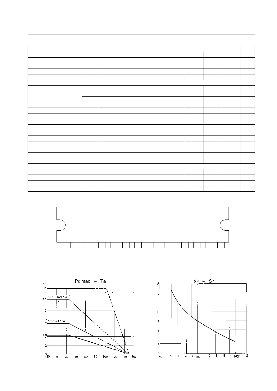
Allowable power dissipation, Pdmax -- W
Heat sink thermal resistance,
f ≠
∞
C/W
Ambient temperature, Ta -- ∞C
Heat sink area, Sf -- cm
2
With infinite heat sink
No heat sink
Aluminum
heat sink
Mounting
torque: 39
N∑cm
With silicon
grease
applied
Aluminum heat sink
(t = 1.5 mm)
Mounting torque: 39 N∑cm
With silicon grease applied
Note: NC pins must not be used (Pins 1 and 14 in the pin assignment figure.)
No. 5969-4/7
LA5633
Block Diagram
CONTROL
TSD
CL
ON/OFF
2
3
1
4
VO1
15.7 V/350 mA
NC
EN1
VO2
9 V/250 mA
EN2
VO3
12 V/100 mA
NC
VO4
5 V/650 mA
CN
GND1
GND2
CONTROL
TSD
CL
ON/OFF
6
7
8
CONTROL
TSD
CL
ON/OFF
5
14
CONTROL
TSD
CL
ON/OFF
13
12
11
9
10
VIN1
VIN2
VIN3
COMP1
GND2
VIN3
COMP2
GND2
VIN3
1.2 V
88 k
12 k
38 k
12 k
A11068
Input
voltage
detection
TSD: Thermal shutdown (protection) circuit
ON/OFF: Output on/off control circuit
CL: Current limiter (overcurrent protection circuit)
Regulator 1
Regulator 2
Regulator 3
Regulator 4
Startup and reference
voltage circuits
No. 5969-5/7
LA5633
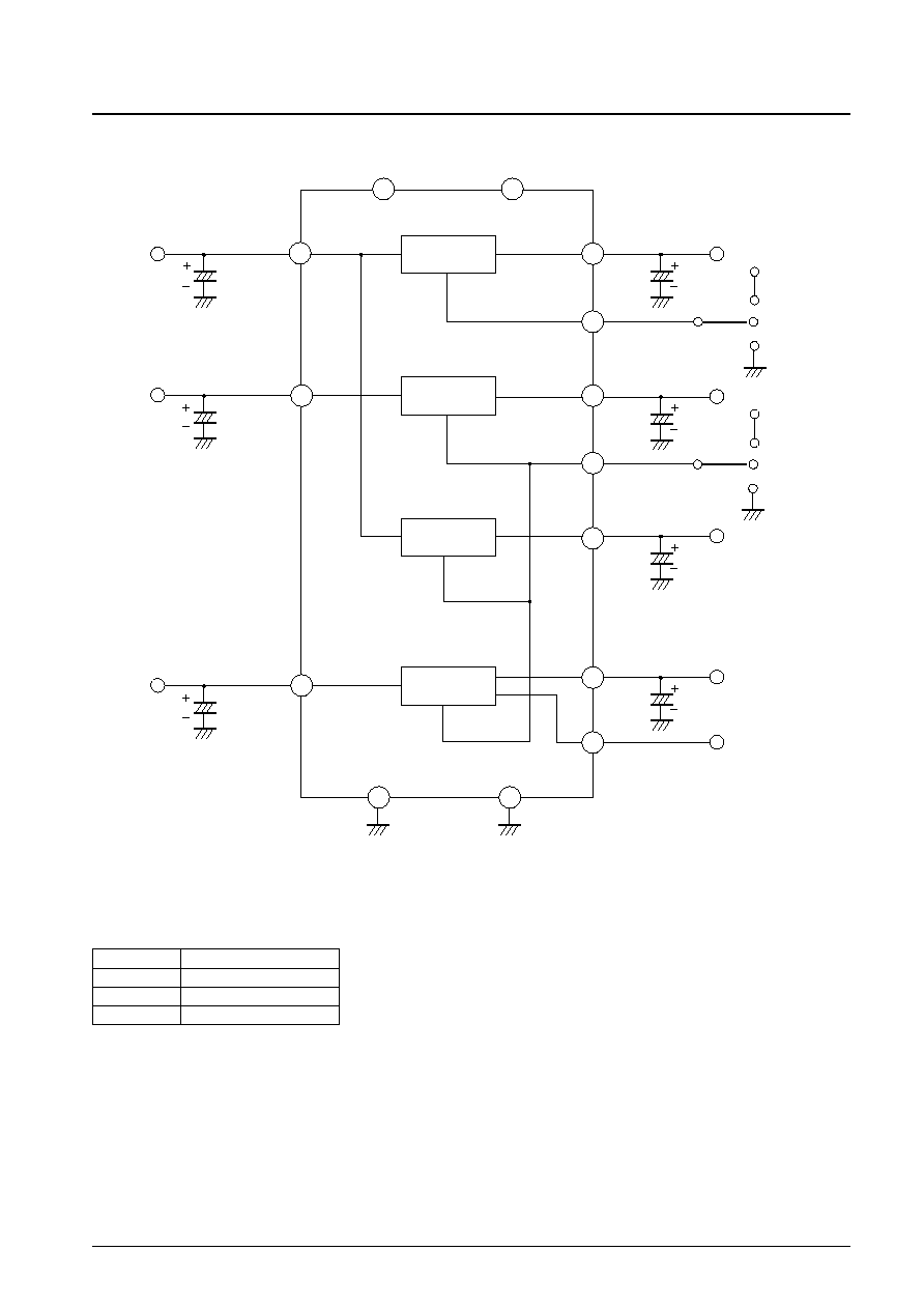
Stipulated Test Circuit
CO2
1
NC
14
3
7
12
10
9
6
4
2
8
5
13
11
NC
100
µ
F
CIN1
Reg1
Reg2
Reg3
Reg4
100
µ
F
CO1
SW1
VEN1
GND1
GND1
GND1
GND2
NC
VO1
EN1
EN2
VO3
VO4
CN
100
µ
F
CIN2
VIN1
VIN2
100
µ
F
CIN3
VIN3
47
µ
F
SW2
VEN2
NC
VO2
CO3
47
µ
F
CO4
100
µ
F
A11069
Function Table
This IC operates as listed in the table under the condition that V
IN
1
V
IN
2
V
IN
3.
∑ H and L in the EN column correspond to high and low input voltage levels, respectively.
∑ H and L in the V
O
column correspond to the output on voltage and the output off voltage, respectively.
∑ The output voltages are controlled independently by the EN lines as follows: EN1 controls VO1, and EN2 controls
V
O
2, V
O
3, and V
O
4 in parallel.
∑ When a given EN is open, the corresponding output will be on.
EN1, EN2
V
O
1, V
O
2/V
O
3/V
O
4
H
L
L
H
Open
H
No. 5969-6/7
LA5633
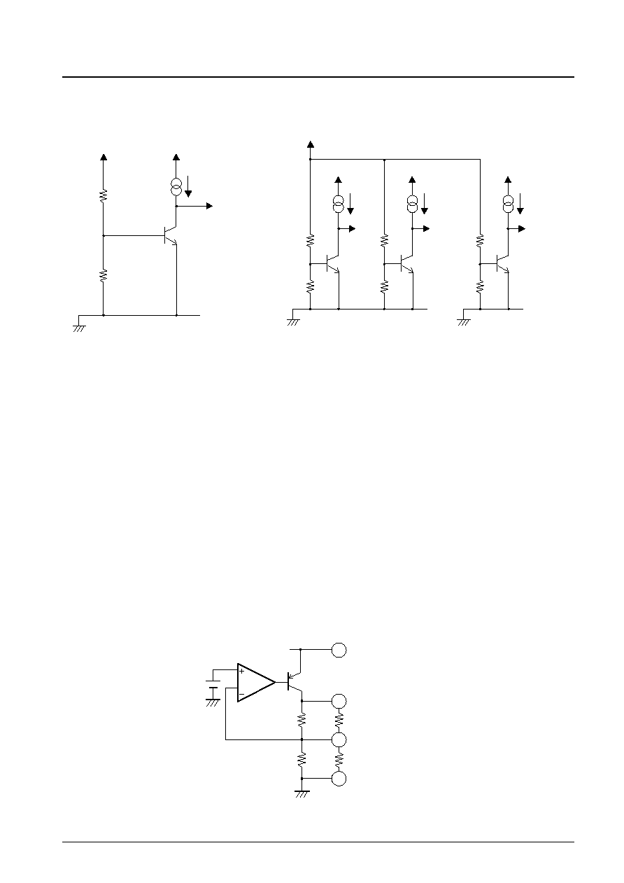
EN (on/off control) Input Block Equivalent Circuit Block Diagram
Usage Notes
∑ GND1 and GND2 are connected through the IC substrate, and must be connected to the lowest potential in the system
and must be connected to identical potentials.
(The functions and characteristics of this IC are not guaranteed if GND1 and GND2 are connected to different potentials.)
∑ The rise and fall of the V
IN
1, V
IN
2, and V
IN
3 voltages must be simultaneous, and none of these pins may be either left
open or connected to ground.
∑ If either V
IN
1 or V
IN
2 are open or at a voltage lower than the stipulated voltage, then the V
O
1 through V
O
4 outputs
will be forcibly turned off to protect the IC.
∑ The output capacitors C
O
1 and C
O
4 must be at least 100 µF, and C
O
2 and C
O
3 must be at least 47 µF. Capacitors with
low temperature coefficients must be use to prevent oscillation at low temperatures.
∑ To assure stable operation, the input capacitors C
IN
1 to C
IN
3 and the output capacitors C
O
1 to C
O
4 must be placed as
close to the IC as possible.
∑ The NC pins (pins 1 and 14) must not be used.
∑ The output voltage V
O
4 can be adjusted by connecting resistors from the CN pin (pin 11) to either V
O
4 or to GND2.
-- To lower V
O
4: Add resistor RA between CN and V
O
4.
-- To raise V
O
4: Add resistor RB between CN and GND2.
Also note that external noise suppression and ripple rejection can be improved by adding an external capacitor at
V
O
4. However, care is required to assure that the system stability (phase margin) is adequate.
∑ Note that these power supplies can be influenced by load fluctuations in the other power supplies.
Sample CN Pin Application Circuit
30 k
120
µ
A
20 k
EN1
30 k
20 k
EN2
VIN1
GND1
GND1
GND2
120
µ
A
VIN2
VIN1
30 k
20 k
120
µ
A
VIN3
30 k
20 k
120
µ
A
A11070
A11071
GND2
10
CN
11
VO4
13
VIN3
12
16 k
5.1 k
RA
RB
1.2 V
Vref
1.2 V
A11072
Control signal
Control signal
Control
signal
Control
signal
V
O
1
V
O
2, V
O
3, V
O
4

PS No. 5969-7/7
LA5633
This catalog provides information as of December, 2001. Specifications and information herein are
subject to change without notice.
Specifications of any and all SANYO products described or contained herein stipulate the performance,
characteristics, and functions of the described products in the independent state, and are not guarantees
of the performance, characteristics, and functions of the described products as mounted in the customer's
products or equipment. To verify symptoms and states that cannot be evaluated in an independent device,
the customer should always evaluate and test devices mounted in the customer's products or equipment.
SANYO Electric Co., Ltd. strives to supply high-quality high-reliability products. However, any and all
semiconductor products fail with some probability. It is possible that these probabilistic failures could
give rise to accidents or events that could endanger human lives, that could give rise to smoke or fire,
or that could cause damage to other property. When designing equipment, adopt safety measures so
that these kinds of accidents or events cannot occur. Such measures include but are not limited to protective
circuits and error prevention circuits for safe design, redundant design, and structural design.
In the event that any or all SANYO products (including technical data, services) described or contained
herein are controlled under any of applicable local export control laws and regulations, such products must
not be exported without obtaining the export license from the authorities concerned in accordance with the
above law.
No part of this publication may be reproduced or transmitted in any form or by any means, electronic or
mechanical, including photocopying and recording, or any information storage or retrieval system,
or otherwise, without the prior written permission of SANYO Electric Co., Ltd.
Any and all information described or contained herein are subject to change without notice due to
product/technology improvement, etc. When designing equipment, refer to the "Delivery Specification"
for the SANYO product that you intend to use.
Information (including circuit diagrams and circuit parameters) herein is for example only; it is not
guaranteed for volume production. SANYO believes information herein is accurate and reliable, but
no guarantees are made or implied regarding its use or any infringements of intellectual property rights
or other rights of third parties.