Ordering number: EN7258
SANYO Electric Co.,Ltd. Semiconductor Company
TOKYO OFFICE Tokyo Bldg., 1-10, 1 Chome, Ueno, Taito-ku, TOKYO, 110-8534 JAPAN
Any and all SANYO products described or contained herein do not have specifications that can handle
applications that require extremely high levels of reliability, such as life-support systems, aircraft's
control systems, or other applications whose failure can be reasonably expected to result in serious
physical and/or material damage. Consult with your SANYO representative nearest you before using
any SANYO products described or contained herein in such applications.
SANYO assumes no responsibility for equipment failures that result from using products at values that
exceed, even momentarily, rated values (such as maximum ratings, operating condition ranges, or other
parameters) listed in products specifications of any and all SANYO products described or contained
herein.
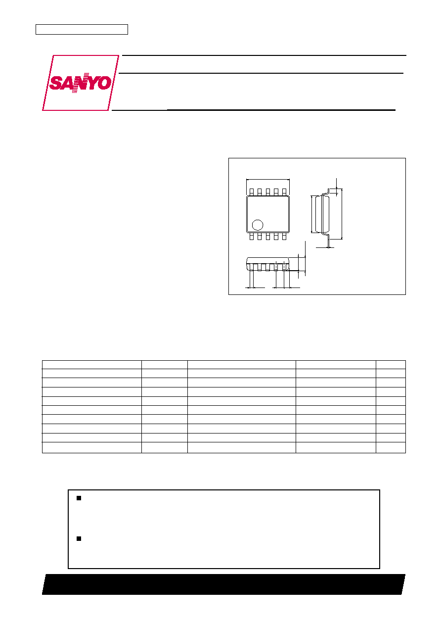
DC/DC Converter Secondary Side Control IC
LA5636M
Monolithic Linear IC
52303AS (II) No.7258-1/7
Overview
The LA5636M is a DC/DC Converter Secondary Side
Control IC that draws power from a car battery and is ideal
for use in rechargers for lithium ion batteries, etc. Because
this IC incorporates only the basic functions (constant
voltage control and constant current control) that are
needed in an IC for charging, it can be easily used in
combination with other ICs for charging.
Features
∑ Includes integrated circuitry for preventing the
malfunction of the system in the event that the input
voltage (car battery voltage) drops.
∑ Produces constant voltage output in proportion to the
PWM input signal. (Permits output voltage control by
microcontroller.)
∑ High-precision reference current (current control amp):
92.5
µA±2.7%
∑ Output voltage can be set through an external resistor.
∑ Each loop of the voltage amp and current amp is
independent.
Package Dimensions
unit: mm
3086B
[3086B]
Maximum Ratings at Ta = 25∞C
Parameter
Symbol
Conditions
Ratings
Unit
Supply voltage
V
CC
max
14.5
V
Allowable power dissipation
Pd max
350
mW
DOUT terminal current/voltage
Idtmax/Vdtmax
1/ ≠0.2 to V
CC
mA/V
PWM input voltage
V
pwm
≠0.2 to 3.0
V
ICONST terminal voltage
VICONST
≠0.2 to V
CC
V
C1 terminal voltage
VC1
≠0.2 to V
CC
V
Operating temperature
Topr1
≠40 to +85
∞C
Performance garanteed temperature
Topr2
≠25 to +75
∞C
Storage temperature
Tstg
≠40 to +150
∞C
Specifications
SANYO: MFP-10S(225mil)
1
10
5
6
(0.5)
1.7max
1.0
0.35
5.0
0.15
6.4
(1.5)
0.1
4.4
0.63
LA5636M
No. 7258-2/7
Electrical Characteristics at Ta = 25∞C, V
CC
=12V
Parameter
Symbol
Conditions
Ratings
Unit
min
typ
max
Operating voltage
V
CC
10.3
13.0
V
Current drain
I
CC
Dout = off, V
pwm
= off, R = 27 k
4
mA
PWM input high voltage
V
pwm
H
1.7
2.9
V
PWM input low voltage
V
pwm
L
0
0.8
V
PWM input current
I
pwm
V
pwm
= 0.0 V
30
nA
PWM input frequency
F
pwm
30
32
37
Hz
Reference voltage 1
V-IN1
V
CC
= 10.5 to 13 V, PWM = L
≠4
2.0 V
+4
%
* Ta = ≠25 to 75∞C
(1.92 V)
(2.08 V)
Reference voltage 2
V-IN2
V
CC
= 10.5 to 13 V, PWM = H
≠6 0.72 V
+6
%
* Ta = ≠25 to 75∞C
(0.68 V)
(0.76 V)
Reference voltage 3
V-IN3
V
CC
= 8.5 V, PWM = L
1.56
--
--
V
* Ta = ≠25 to 75∞C
Reference voltage 4
V-IN4
V
CC
= 8.5 V, PWM = H
0.59
--
--
V
* Ta = ≠25 to 75∞C
Reference current
IREF
V
CC
= 10.5 to 13 V, when 27 k
is connected
90.0
92.5
95.0
µA
* Ta = ≠25 to 75∞C
* The design is guaranteed over the temperature range, so the temperature is not measured.
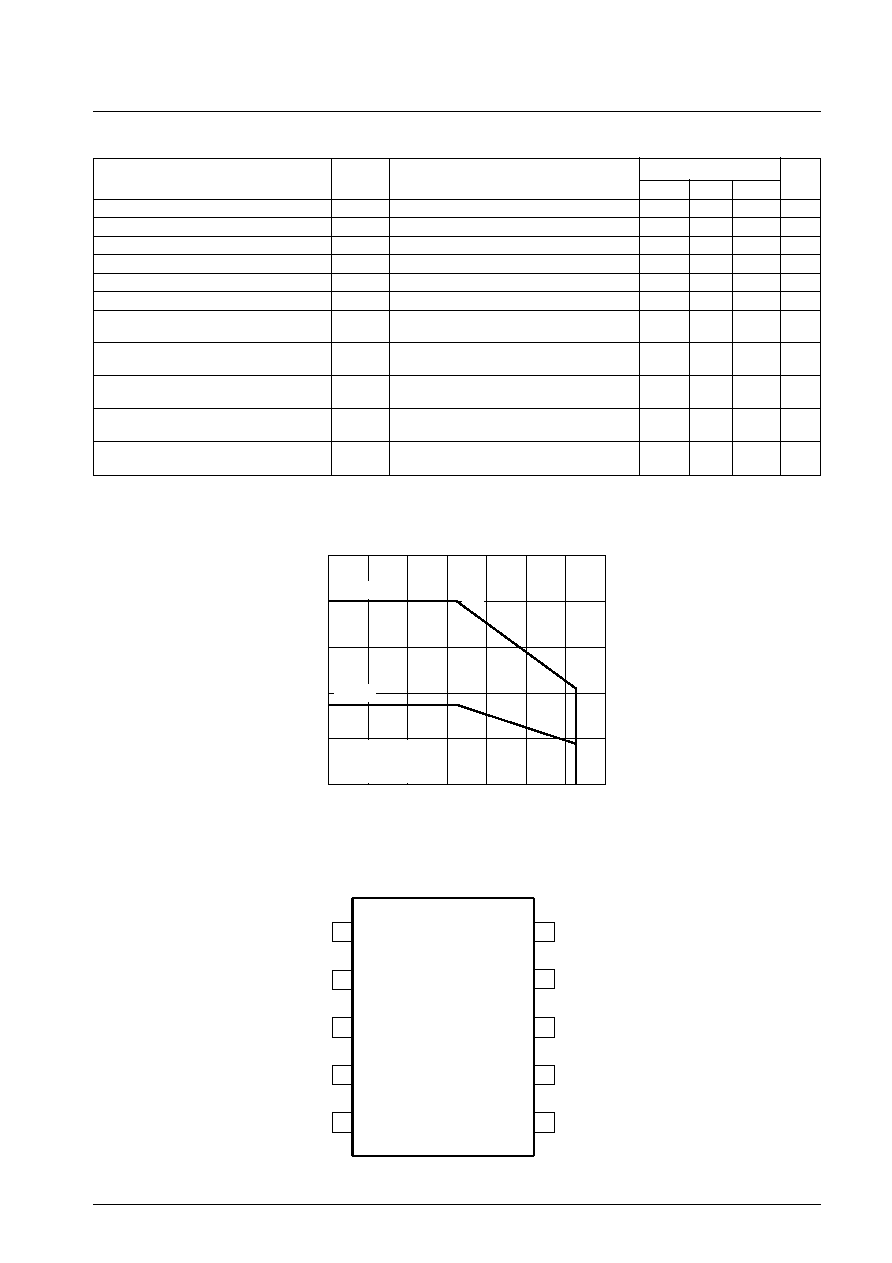
0
20
--40
--20
40
60
100
80
0
1.0
0.8
0.6
0.4
0.2
ILA00995
Pd max -- Ta
0.18
0.42
0.80
0.35
With specified
board
IC alone
Specified board
76.1
◊ 114.3 ◊ 1.6 mm
3
Glass epoxy resin
Allo
w
a
b
le po
w
er dissipation Pd max
≠
W
Ambient temperature Ta ≠ ∞C
Pin Assignment
2
V+IN
10
1
3
4
5
6
7
8
9
V-IN
C1
ISEN+IN
ISEN-IN
GND
ICONST
DOUT
PWM
V
CC
LA5636M
Top view