 | –≠–ª–µ–∫—Ç—Ä–æ–Ω–Ω—ã–π –∫–æ–º–ø–æ–Ω–µ–Ω—Ç: LA5657H | –°–∫–∞—á–∞—Ç—å:  PDF PDF  ZIP ZIP |
Ordering number : ENN7596
52804TN (OT) No. 7596-1/8
Overview
The LA5657H provides 10 V/2.2 A and 5 V/1.4 A
external pnp transistor based low-saturation regulators
with standby functions, as well as 3.3 V, 5 V, and 8 V
constant voltage, open collector, and VCC linked (VCC -
1 V) outputs that can be controlled from serial data (CCB).
It also includes three reset detection circuits for the VDD,
ACC, and battery systems. The LA5657H is an optimal
power supply IC for car audio systems and similar
products.
Features
∑ Built-in 10 V and 5 V regulators (external pnp transistor
required) with standby (on/off) functions
∑ Extensive set of output systems: two 8 V systems, single
5 V, 3.25 V, and 5 to 9.7 V (set with an external resistor)
systems, four open-collector output systems, and two
V
CC
linked systems.
∑ Three reset circuits: A
CC
, V
DD
(with delay circuit), and
BATT
∑ Full complement of protection circuits
-- Overcurrent protection circuits for all output systems
except the open collector and reset circuits
-- Thermal protection circuits for all outputs except the
reset circuits
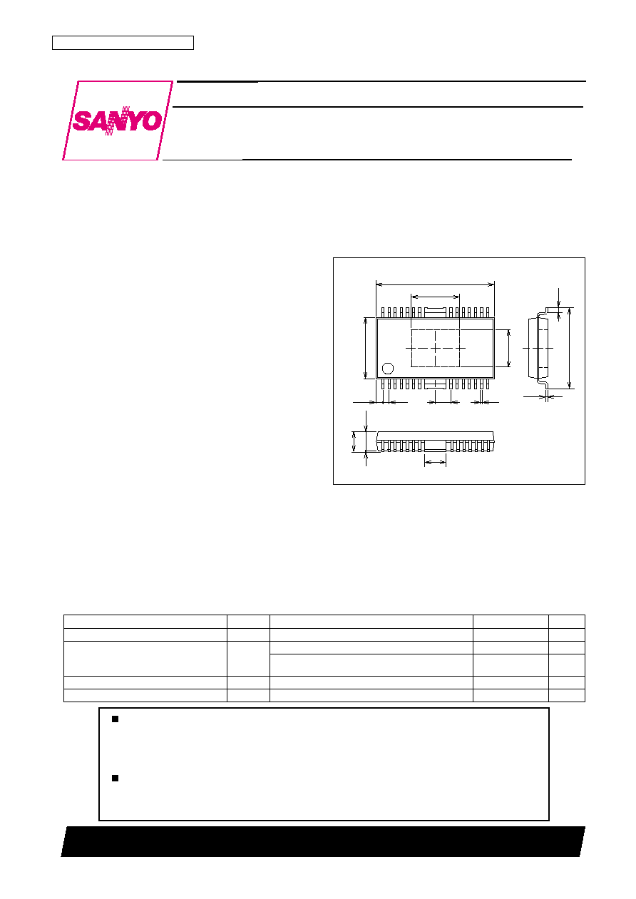
Package Dimensions
unit: mm
3233A-HSOP28H
(6.2)
28
15
1
14
0.8
15.2
2.7
0.3
4.9
10.5
0.65
0.25
(0.8)
7.9
(2.25)
2.45max
0.1
2.0
SANYO: HSOP28H (375 mil)
[LA5657H]
LA5657H
SANYO Electric Co.,Ltd. Semiconductor Company
TOKYO OFFICE Tokyo Bldg., 1-10, 1 Chome, Ueno, Taito-ku, TOKYO, 110-8534 JAPAN
System Power Supply IC for Car AV Systems
Monolithic Digital IC
Any and all SANYO products described or contained herein do not have specifications that can handle
applications that require extremely high levels of reliability, such as life-support systems, aircraft's
control systems, or other applications whose failure can be reasonably expected to result in serious
physical and/or material damage. Consult with your SANYO representative nearest you before using
any SANYO products described or contained herein in such applications.
SANYO assumes no responsibility for equipment failures that result from using products at values that
exceed, even momentarily, rated values (such as maximum ratings, operating condition ranges, or other
parameters) listed in products specifications of any and all SANYO products described or contained
herein.
Parameter
Symbol
Conditions
Ratings
Unit
Maximum supply voltage
V
CC
max
24
V
Ta
25∞C, independent IC
0.82
W
Allowable power dissipation
Pd max
Ta
25∞C, mounted on a 76.1
◊
114.3
◊
1.6 mm glass
2.0
W
epoxy printed circuit board
Operating temperature
Topr
≠30 to +85
∞C
Storage temperature
Tstg
≠55 to +150
∞C
Specifications
Absolute Maximum Ratings
at Ta = 25∞C
No. 7596-2/8
LA5657H
Parameter
Symbol
Conditions
Ratings
Unit
Supply voltage
V
CC
COM10V output, normal operation
10.3 to 18
V
COM5V output, normal operation
5.3 to 18
V
STBY pin input voltage
VST OFF
Output off control voltage
0 to 1
V
VST ON
Output on control voltage
2.5 to 5
V
COM10V output current
I
O
1
Within the ASO for
mA
the external transistor
COM5V output current
I
O
2
Within the ASO for
mA
the external transistor
LCDV output current
I
O
3
0 to 30
mA
TAPE8V output current
I
O
4
0 to 30
mA
RD8V output current
I
O
5
0 to 200
mA
DSP5V output current
I
O
6
0 to 100
mA
DSP3.25V output current
I
O
7
0 to 100
mA
AMP+B output current
I
O
8
0 to 100
mA
ANT+B output current
I
O
9
0 to 250
mA
CAP MR output current
I
O
10
0 to 10
mA
P1 output sink current
I
O
11
0 to 10
mA
P2 output sink current
I
O
12
0 to 10
mA
P3 output sink current
I
O
13
0 to 10
mA
ACCRO output sink current
I
O
-ACCR
0 to 1
mA
V
DD
RST output sink current
I
O
-V
DD
R
0 to 1
mA
BATRO output sink current
I
O
-BATR
0 to 5
mA
Recommended Operating Ranges
at Ta = 25∞C
Parameter
Symbol
Conditions
Ratings
Unit
min
typ
max
Current drain 1
I
CC
1
VSTBY = 0 V, BATRO = High, RESET = High,
150
170
µA
ACCRO = Low
Current drain 2
I
CC
2
VSTBY = 5 V, Serial data control outputs: all off
19
25
mA
BATRO, RESET, and ACCRO outputs: all high
[V
DD
Reset Block
*
1
]
Reset threshold voltage
VTVDDR
4.05
4.25
4.45
V
Hysteresis
VHVDDR
50
80
130
mV
Low-level output voltage
VOLVDDR
ISINK = 50 µA
0.25
0.4
V
High-level output voltage
VOHVDDR
Resistance between RESET and ground: 1 M
0.8 V
DD
V
DD
V
CDLY outflow current
ICDLY
CDLY outflow current
≠4.0
≠3.4
≠2.8
µA
CDLY threshold voltage
VTHCDLY
1.18
1.25
1.32
V
[BAT Reset Block
*
2
]
Reset threshold voltage
VTBATR
1.21
1.25
1.29
V
Hysteresis
VHBATR
163
233
326
mV
Leakage current
ILKBATR
≠2
µA
Low-level output voltage
VOLBATR
ISINK = 50 µA
0.25
0.4
V
High-level output voltage
VOHBATR
Resistance between BATRO and ground: 1 M
0.8 V
DD
V
DD
V
[ACC Reset Block
*
2
]
Reset threshold voltage
VTACCR
1.21
1.25
1.29
V
Hysteresis
VHACCR
10
20
30
mV
Leakage current
ILKACCR
≠2
µA
Low-level output voltage
VOLACCR
ISINK = 1 mA
0.35
0.5
V
High-level output voltage
VOHACCR
Resistance between ACCRO and ground: 1 M
0.8 V
DD
V
DD
V
Electrical Characteristics
at Ta = 25∞C, V
CC
= 13.2 V, in the specified test circuit
Continued on next page.
No. 7596-3/8
LA5657H
Parameter
Symbol
Conditions
Ratings
Unit
min
typ
max
[COM10V Output (V
CC
= 13.2 V, VSTBY = 5 V, I
O
2 = 2.2 A)]
Output voltage
V
O
1
External transistor: 2SB921
9.55
10
10.45
V
Dropout voltage
VDROP1
V
CC
= 9.55 V
0.3
0.6
V
Line regulation
VOLN1
11.15 V
V
CC
18 V
30
300
mV
Load regulation
VOLD1
0
I
O
1
2.2 A
200
800
mV
Control input current
ICONT1
20
22
26.4
mA
Output off voltage
V
O
1 OFF
0.2
V
Ripple rejection (reference value)
RREJ1
f = 120 Hz, 11.15 V
V
CC
18 V
70
dB
[COM5V Output (V
CC
= 13.2 V, VSTBY = 5 V, I
O
2 = 1.4 A)]
Output voltage
V
O
2
External transistor: 2SB921
4.775
5
5.225
V
Dropout voltage
VDROP2
V
CC
= 4.775 V
0.3
0.6
V
Line regulation
VOLN2
5.925 V
V
CC
18 V
30
300
mV
Load regulation
VOLD2
0
I
O
2
1.4 A
200
800
mV
Control input current
ICONT2
15
16.7
20.2
mA
Output off voltage
V
O
2 OFF
0.2
V
Ripple rejection (reference value)
RREJ2
f = 120 Hz, 5.925 V
V
CC
18 V
70
dB
[LCDV Output (V
CC
= 13.2 V, VSTBY = 5 V, I
O
2 = 30 mA, CN pin: open)]
Output voltage
V
O
3
4.85
5
5.15
V
Dropout voltage
VDROP3
V
CC
= 4.85 V
0.3
0.6
V
Line regulation
VOLN3
5.85 V
V
CC
18 V
50
75
mV
Load regulation
VOLD3
0
I
O
2
30 mA
100
150
mV
Peak output current
IOP3
30
mA
Output short current
IOSC3
60
mA
(reference value)
Output off voltage
V
O
3 OFF
0.2
V
[TAPE8V Output (V
CC
= 13.2 V, VSTBY = 5 V, I
O
4 = 30 mA)]
Output voltage
V
O
4
7.64
8
8.36
V
Dropout voltage
VDROP4
V
O
1 = 7.6 V
1.0
1.4
V
Line regulation
VOLN4
9.9 V
V
CC
18 V
50
75
mV
Load regulation
VOLD4
0
I
O
4
30 mA
100
150
mV
Peak output current
IOP4
30
mA
Output short current
IOSC4
220
mA
(reference value)
Output off voltage
V
O
4 OFF
0.2
V
[RD8V Output (V
CC
= 13.2 V, VSTBY = 5 V, I
O
5 = 200 mA)]
Output voltage
V
O
5
7.64
8
8.36
V
Dropout voltage
VDROP5
V
O
1 = 7.6 V
1.0
1.4
V
Line regulation
VOLN5
9.96 V
V
CC
18 V
50
75
mV
Load regulation
VOLD5
0
I
O
5
200 mA
100
150
mV
Peak output current
IOP5
200
mA
Output short current
IOSC5
900
mA
(reference value)
Output off voltage
V
O
5 OFF
0.2
V
[DSP5V Output (V
CC
= 13.2 V, VSTBY = 5 V, I
O
6 = 100 mA)]
Output voltage
V
O
6
4.775
5
5.225
V
Dropout voltage
VDROP6
V
O
1 = 4.775 V
1.0
1.4
V
Line regulation
VOLN6
6.825 V
V
CC
18 V
50
75
mV
Load regulation
VOLD6
0
I
O
6
100 mA
100
150
mV
Peak output current
IOP6
100
mA
Output short current
IOSC6
520
mA
(reference value)
Output off voltage
V
O
6 OFF
0.2
V
Continued from preceding page.
Continued on next page.

No. 7596-4/8
LA5657H
Parameter
Symbol
Conditions
Ratings
Unit
min
typ
max
[DSP3.25V Output (V
CC
= 13.2 V, VSTBY = 5 V, I
O
7 = 100 mA)]
Output voltage
V
O
7
3.104
3.25
3.396
V
Dropout voltage
VDROP7
V
O
2 = 3.104 V
1.0
1.4
V
Line regulation
VOLN7
4.996 V
V
CC
18 V
50
75
mV
Load regulation
VOLD7
0
I
O
7
100 mA
100
150
mV
Peak output current
IOP7
100
mA
Output short current
IOSC7
420
mA
(reference value)
Output off voltage
V
O
7 OFF
0.2
V
[AMP + B Output (V
CC
= 13.2 V, VSTBY = 5 V, I
O
8 = 100 mA)]
Output voltage
V
O
8
11.7
12.2
V
Dropout voltage
VDROP8
1
1.5
V
Peak output current
IOP8
100
mA
Output short current
IOSC8
300
mA
(reference value)
Output off voltage
V
O
8 OFF
0.2
V
[ANT + B Output (V
CC
= 13.2 V, VSTBY = 5 V, I
O
9 = 250 mA)]
Output voltage
V
O
9
11.7
12.2
V
Dropout voltage
VDROP9
1
1.5
V
Peak output current
IOP9
250
mA
Output short current
IOSC9
700
mA
(reference value)
Output off voltage
V
O
9 OFF
0.2
V
[CAP MR Output (V
CC
= 13.2 V, VSTBY = 5 V, I
O
10 = 10 mA)]
Dropout voltage
VDROP10
0.4
0.8
V
Output sink current
I
O
10
10
mA
[P1 (ILL) Output (V
CC
= 13.2 V, VSTBY = 5 V, I
O
11 = 10 mA)]
Dropout voltage
VDROP11
0.4
0.8
V
Output sink current
I
O
11
10
mA
[P2 (LCD) Output (V
CC
= 13.2 V, VSTBY = 5 V, I
O
12 = 10 mA)]
Dropout voltage
VDROP12
0.4
0.8
V
Output sink current
I
O
12
10
mA
[P3 (CAP MR) Output (V
CC
= 13.2 V, VSTBY = 5 V, I
O
13 = 10 mA)]
Dropout voltage
VDROP13
0.4
0.8
V
Output sink current
I
O
13
10
mA
[Thermal Protection Circuit]
Operating temperature
*
3
TSD
V
O
1 and V
O
2 operation
150
175
∞C
V
O
3 to V
O
13 linked to V
O
1 and V
O
2 operation.
Continued from preceding page.
Notes on items
*
1 to
*
3.
(1) V
DD
reset block (
*
1)
∑ The reset detection function detects the level of V
DD
5V input to V
DD
IN.
∑ This reset function operates correctly when the V
DD
IN voltage is over 0.5 V, but is undefined when V
DD
IN is under 0.5 V. The reset voltage must never
exceed V
DD
IN.
∑ The allowable range for the threshold voltage has a tolerance of ±4.7%.
(2) BAT and ACC reset blocks (
*
2)
∑ These reset detection outputs must operate correctly when the V
DD
IN voltage is over 2 V. The reset voltages must never exceed V
DD
IN.
∑ The ACC detection function has no region where detection is unpredictable according to the value of the voltage detected. That is, the low level will be
detected correctly when ACC IN is 0 V.
∑ The allowable range for the threshold voltage has a tolerance of ±3.2%.
(3) Thermal protection and operating temperature (
*
3)
∑ The values shown are design target values and are not tested.
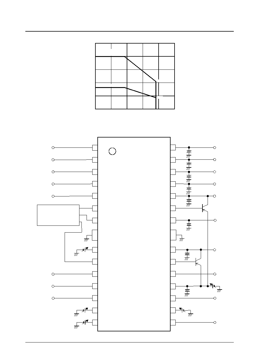
Pin Assignment and Test Circuit
No. 7596-5/8
LA5657H
Pd max -- Ta
Allowable power dissipation, Pd max
--
W
Ambient temperature, Ta --
∞
C
0
0.5
1.0
1.5
2.0
2.5
≠30
2.00
1.04
0.82
0.43
0
30
60
90
120
ILA06471
Mounted on a
circuit board
Independent IC
P1(ILL)
AMP+B
ANT+B
ACCRO
BATRO
RESET
CL
DI
CN
LCDV
P3(M2F)
P2(LCD)
7
1
2
3
4
5
6
13
12
8
9
10
11
14
COM5V
CDLY
VDD IN
BAT IN
DSP5V
RD8V
CONT2
COM10V
CAP MR
TAPE8V
ACC IN
DSP3.25V
15
16
17
18
19
21
28
27
26
25
24
23
22
20
Top view
CE
GND
STBY
GND
VCC
CONT1
VSTB
+
C05
+
C06
+
C04
+
C03
33
µ
F
+
C07
+
C01
+
CIN
+
C02
VACCIN
VBATIN
VVDDIN
2SB921
2SB921
VCC
CCB serial signal
generator
22
µ
F
22
µ
F
22
µ
F
33
µ
F
22
µ
F
33
µ
F
100
µ
F