 | –≠–ª–µ–∫—Ç—Ä–æ–Ω–Ω—ã–π –∫–æ–º–ø–æ–Ω–µ–Ω—Ç: LA6538T | –°–∫–∞—á–∞—Ç—å:  PDF PDF  ZIP ZIP |
Ordering number : ENN6518
83000RM (OT) No. 6518-1/6
Overview
The LA6538T is optimal for use as a fan motor driver in
equipment, such as notebook personal computers and
electronic game units, that requires miniaturization and
low noise levels. This device achieves highly efficient
single-phase bipolar fan motor drive by providing a low
saturation voltage BTL output.
Functions and Features
∑ BTL output single-phase full-wave linear drive (gain
resistance: 180 to 500 k
, 360
◊
)
-- Since this device generates no switching noise, it is
optimal for fan drive in audio equipment, electronic
games, and notebook personal computers.
∑ Supports low-voltage operation and features a wide
usable voltage range (V
CC
= 2.5 to 9.5 V).
∑ Low saturation voltage output (Upper side + lower side
saturation voltage: V
O
sat(total) = 0.2 V (typ),
I
O
= 100 mA)
-- This device achieves a high coil efficiency for low
current drain, and generates minimal heat in the IC
itself.
∑ Constant-voltage Hall bias output.
-- The Hall element is regulated at 2.1 V, and the
device provides a stable Hall output with excellent
temperature characteristics.
∑ FG output
-- The LA6538T provides a speed detection output (an
open-collector output).
∑ Built-in thermal protection circuit
-- This circuit limits the drive current to prevent
damage to or destruction of the IC when the IC chip
temperature exceeds 180∞C due to excessive output
current caused by load shorting or other problem.
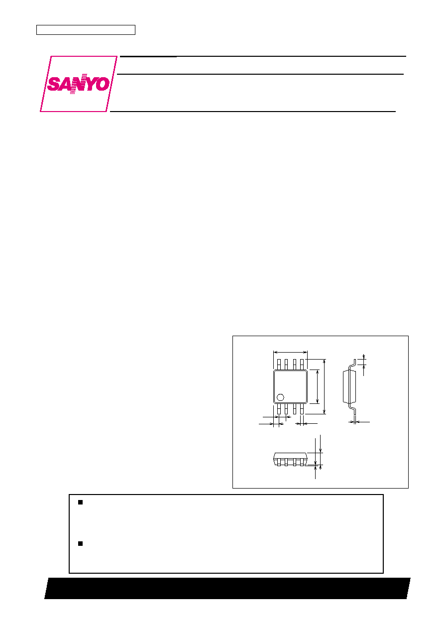
∑ Ultraminiature package
(MSOP-8: 3.0
◊
4.9
◊
0.93 mm
3
)
-- Allows the circuit board to be miniaturized and a
large heat sink to be used.
Reference materials:
T package (MSOP-8) series fan motor drivers
LB1964T: 3 and 5 V operation, low saturation voltage
switching single-phase bipolar drive, FG output
LB11963T: 5 and 12 V operation, switching single-
phase bipolar drive, restart circuit, lock detection, 1/2
FG output
LB11964T: 5 and 12 V operation, switching single-
phase bipolar drive, restart circuit, lock detection, FG
output
Package Dimensions
unit: mm
3245-MSOP8
4.9
3.0
0.65
3.0
(0.5)
(0.85)
0.5
0.25
1
4
8
5
0.25
0.08
1.1max
SANYO: MSOP8
[LA6538T]
LA6538T
SANYO Electric Co.,Ltd. Semiconductor Company
TOKYO OFFICE Tokyo Bldg., 1-10, 1 Chome, Ueno, Taito-ku, TOKYO, 110-8534 JAPAN
Single-Phase Full-Wave Fan Motor Driver
Monolithic Linear IC
Any and all SANYO products described or contained herein do not have specifications that can handle
applications that require extremely high levels of reliability, such as life-support systems, aircraft's
control systems, or other applications whose failure can be reasonably expected to result in serious
physical and/or material damage. Consult with your SANYO representative nearest you before using
any SANYO products described or contained herein in such applications.
SANYO assumes no responsibility for equipment failures that result from using products at values that
exceed, even momentarily, rated values (such as maximum ratings, operating condition ranges, or other
parameters) listed in products specifications of any and all SANYO products described or contained
herein.
No. 6518-2/6
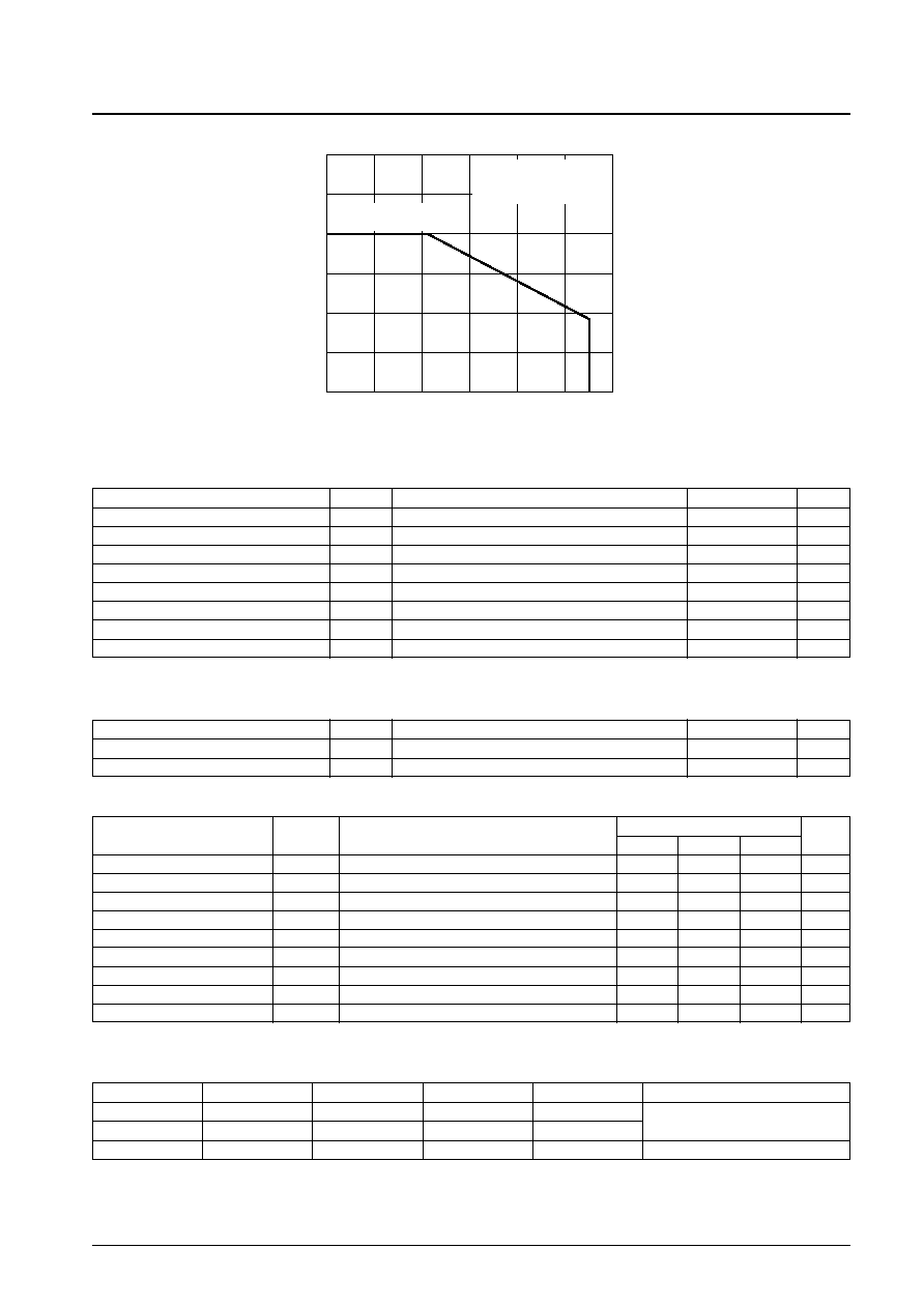
LA6538T
Parameter
Symbol
Conditions
Ratings
Unit
Maximum supply voltage
V
CC
max
10
V
Allowable power dissipation
Pd max
Mounted on the specified printed circuit board
*
400
mW
OUT pin output current
I
OUT
max
0.3
A
OUT pin output voltage handling
V
OUT
max
9.5
V
FG output voltage handling
V
FG
max
10
V
FG output current
I
FG
max
5
mA
Operating temperature
Topr
≠20 to +90
∞C
Storage temperature
Tstg
≠55 to +150
∞C
Note:
*
Specified printed circuit board: 20.0
◊
10.0
◊
0.8 mm
3
paper phenolic board, wiring density: 20%.
Specifications
Maximum Ratings
at Ta = 25∞C
Parameter
Symbol
Conditions
Ratings
Unit
Supply voltage
V
CC
2.5 to 9.5
V
Hall input common-mode input voltage range
V
ICM
0.9 to V
CC
≠ 1
V
Recommended Operating Conditions
at Ta = 25∞C
ILA00211
Pd max -- Ta
0
600
500
300
400
100
200
192
80
100
0
--20
20
40
60
Allowable power dissipation, Pdmax -- mW
Ambient temperature, Ta -- ∞C
Mounted on the specified
printed circuit board
Specified printed circuit board:
20.0
◊
10.0
◊
0.8 mm
3
Paper phenolic board
Parameter
Symbol
Conditions
Ratings
Unit
min
typ
max
Circuit current
I
CC
IN
≠
= 2.6 V, IN
+
= 2.4 V, R
L
=
10
15
mA
OUT pin output low-level voltage
V
O
L
I
O
= 100 mA
0.1
0.2
V
OUT pin output high-level voltage
V
O
H
I
O
= 100 mA
0.1
0.2
V
Hall bias voltage
V
HB
RH = 360
+ 91
1.9
2.1
2.3
V
Hall amplifier gain
VG
47
50
53
dB
Hall amplifier input resistance
V
INR
400
500
620
FG output low-level voltage
V
FG
I
FG
= 3 mA
0.2
0.3
V
FG output leakage current
I
FGL
V
FG
= 7 V
30
µA
Thermal protection circuit
T-TSD
Design guarantee
*
150
180
200
∞C
Electrical Characteristics
at Ta = 25∞C, V
CC
= 5 V
Note:
*
Design guarantee: Indicates a design target value. These parameters are not tested in the independent IC.
Truth Table
IN
≠
IN
+
OUT1
OUT2
FG
Mode
H
L
H
L
L
Motor operating
L
H
L
H
off
--
--
off
off
--
Thermal protection activated
No. 6518-3/6
LA6538T
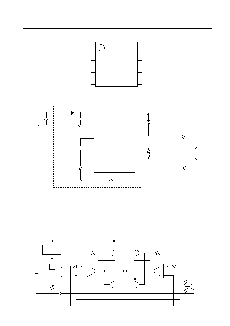
Pin Assignment
IN+
1
2
3
4
HB
8
7
6
5
IN--
OUT1
FG
VCC
OUT2
GND
Top view
LA6538T
ILA00206
Sample Application Circuit
IN+
HB
IN--
FG
R2
R2
OUT1
OUT2
Di
V
CC
V
CC
Cr
*
1
*
2
R1
GND
ILA00207
ILA00208
H
*
3
*
4
H
Notes: 1. When the diode Di is used to prevent device destruction from reverse connection, the capacitor Cr must be inserted to assure a path for
regenerative currents. Similarly, if there are no nearby capacitors on the fan power supply line, the capacitor Cr is also required to increase
reliability.
2. The Hall element is biased at a constant voltage of approximately 2.1 V from the HB pin. Thus the LA6538T provides a stable Hall output with
excellent temperature characteristics. The resistor R1 adjusts the Hall output amplitude.
The LA6538T implements linear drive by amplifying the Hall output and applying voltage control to the motor coils. Startup characteristics and
efficiency are improved by using a higher Hall device output. However, the motor can be made to operate more quietly by adjusting the Hall device.
3. If the Hall bias is taken from V
CC
, bias the Hall device at 1/2 V
CC
as shown in the figure.
4. This pin must be left open if unused.
Devices on the
printed circuit board
Block Diagram
180 k
500
ILA00209
HB
FG
IN+
IN--
GND
OUT1
OUT2
V
CC
H
180 k
500
2.1 VRG
No. 6518-4/6
LA6538T
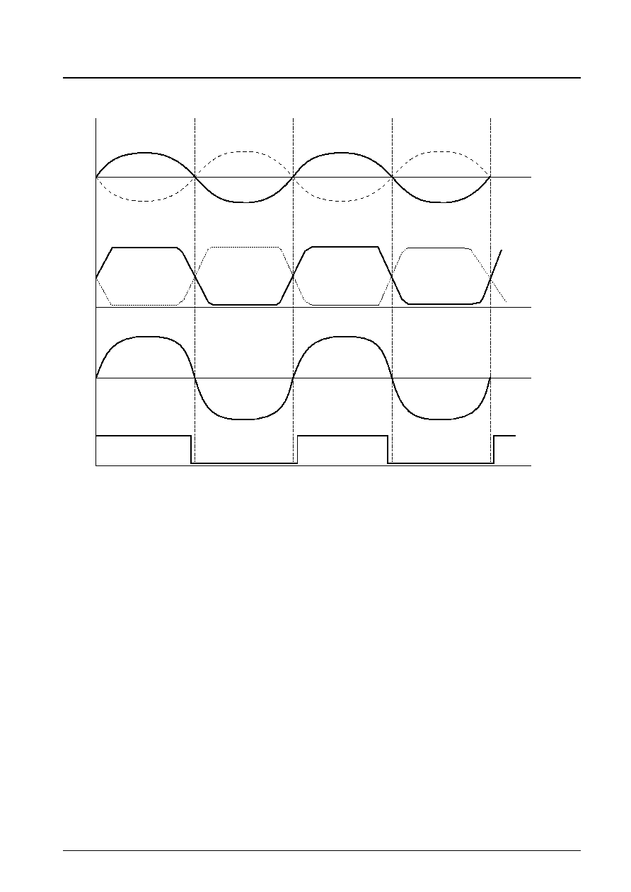
Timing Chart
ILA00210
Hall Signal
OUTPUT
Coil Current
FG Pulse
No. 6518-5/6
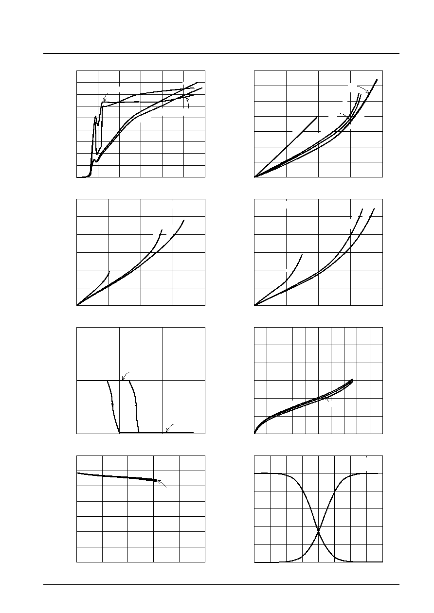
LA6538T
ILA00212
I
CC
-- V
CC
IN-- = IN+ = HB
IN
+ = L
IN
-- = L
IN-- = IN+ = 1/2 V
CC
0
18
16
14
12
4
2
8
10
6
8
12
0
4
6
10
2
ILA00213
V
O
(sat) -- I
O
0
0.7
0.6
0.5
0.3
0.4
0.2
0.1
300
200
400
0
100
ILA00214
V
O
(sat) -- I
O
0
0.6
0.5
0.4
0.3
0.1
0.2
300
400
0
100
200
ILA00215
ILA00216
V
FG
L
H
2
3
0
1
ILA00217
V
FG
(sat) -- I
FG
0
0.6
0.5
0.4
0.3
0.2
0.1
5
1
2
3
4
6
7
8
9
10
0
ILA00218
V
HB
-- I
HB
0
2.8
2.4
2.0
1.6
0.4
0.8
1.2
8
6
4
2
10
0
ILA00219
(IN--) -- (IN+) -- mV
0
6
5
4
3
2
1
20
30
0
40
--40
--30
--20
--10
10
V
CC
= 8.5 V
OUT1(PNP)
total
OUT1(NPN)
OUT2(NPN)
OUT2(PNP)
V
CC
= 5 V
V
CC
= 5 V
FG = "H"
FG = "L"
PNP 3
V
PNP 5
V
PNP 8
V
3 V
9 V
V
O
(sat) -- I
O
0
0.6
0.5
0.4
0.3
0.1
0.2
300
400
0
100
200
NPN 3
V
NPN 5
V
NPN 8
V
5 V
3 V
9 V
5 V
Current drain, I
CC
-- mA
Output saturation voltage, V
O
(sat) -- V
Output saturation voltage, V
O
(sat) -- V
Output saturation voltage, V
O
(sat) -- V
Supply voltage, V
CC
-- V
Output current, I
O
-- mA
Output current, I
O
-- mA
Output current, I
O
-- mA
FG Threshold Level
OUT2 pnp (upper side)
OUT1 npn (lower side)
Saturation voltage, V
FG
(sat) -- V
Output voltage, V
O
-- V
Hall bias voltage, V
HB
-- V
Output voltage, V
OUT
2 -- V
FG supply current, I
FG
-- mA
Hall bias current, I
HB
-- mA
Gain Characteristics
V
CC
= 5 V
1/2 V
CC
bias
PS No. 6518-6/6
LA6538T
This catalog provides information as of August, 2000. Specifications and information herein are subject to
change without notice.
Specifications of any and all SANYO products described or contained herein stipulate the performance,
characteristics, and functions of the described products in the independent state, and are not guarantees
of the performance, characteristics, and functions of the described products as mounted in the customer's
products or equipment. To verify symptoms and states that cannot be evaluated in an independent device,
the customer should always evaluate and test devices mounted in the customer's products or equipment.
SANYO Electric Co., Ltd. strives to supply high-quality high-reliability products. However, any and all
semiconductor products fail with some probability. It is possible that these probabilistic failures could
give rise to accidents or events that could endanger human lives, that could give rise to smoke or fire,
or that could cause damage to other property. When designing equipment, adopt safety measures so
that these kinds of accidents or events cannot occur. Such measures include but are not limited to protective
circuits and error prevention circuits for safe design, redundant design, and structural design.
In the event that any or all SANYO products (including technical data, services) described or contained
herein are controlled under any of applicable local export control laws and regulations, such products must
not be exported without obtaining the export license from the authorities concerned in accordance with the
above law.
No part of this publication may be reproduced or transmitted in any form or by any means, electronic or
mechanical, including photocopying and recording, or any information storage or retrieval system,
or otherwise, without the prior written permission of SANYO Electric Co., Ltd.
Any and all information described or contained herein are subject to change without notice due to
product/technology improvement, etc. When designing equipment, refer to the "Delivery Specification"
for the SANYO product that you intend to use.
Information (including circuit diagrams and circuit parameters) herein is for example only; it is not
guaranteed for volume production. SANYO believes information herein is accurate and reliable, but
no guarantees are made or implied regarding its use or any infringements of intellectual property rights
or other rights of third parties.