
81004TN(OT) No.7819-1/8
Any and all SANYO products described or contained herein do not have specifications that can handle
applications that require extremely high levels of reliability, such as life-support systems, aircraft's control
systems, or other applications whose failure can be reasonably expected to result in serious physical and/or
material damage. Consult with your SANYO representative nearest you before using any SANYO products
described or contained herein in such applications.
SANYO assumes no responsibility for equipment failures that result from using products at values that
exceed, even momentarily, rated values (such as maximum ratings, operating condition ranges, or other
parameters) listed in products specifications of any and all SANYO products described or contained herein.
SANYO Electric Co., Ltd. Semiconductor Company
TOKYO OFFICE Tokyo Bldg., 1-10, 1 chome, Ueno, Taito-ku, TOKYO, 110-8534 JAPAN
SANYO Semiconductors
DATA SHEET
LA6575H
Monolithic Digital IC
Five-Channel Driver (four BTL
channels plus one H bridge channel)
for MD and CD Player
Overview
The LA6575H is a five-channel motor driver IC for MD and CD players with four BTL channels and one H bridge
channel for the loading motor. It features a built-in 5 V regulator circuit.
Functions and Features
� Four power amplifier channels plus one H bridge channel
� I
O
max: 700 mA (each channel)
� Built-in level shifting circuits for the BLT amplifiers
� One muting circuit system (output on/off control): applies to the BTL amplifiers
� Thermal protection circuit (Thermal shutdown circuit)
� Separate loading block power supply
� Built-in 5 V regulator
Specifications
Maximum Ratings at Ta 25 C
Parameter
Symbol
Conditions
Ratings
Unit
Supply voltage
V
CC
max
14
V
Independent IC
0.82
Allowable power dissipation
Pdmax
Mounted on a board.
2.0
W
Maximum output current
I
O
max
Each channel for CH1 to CH5
0.7
A
Maximum input voltage
VINB
13
V
MUTE pin voltage
VMUTE
13
V
Operating temperature
Topr
30 to 85
C
Storage temperature
Tstg
55 to 150
C
Note : Mounted on a board (76.1 114.3 1.6 mm) Material: glass epoxy
Recommended Operating Conditions at Ta 25 C
Parameter
Symbol
Conditions
Ratings
Unit
Supply voltage
V
CC
5.6 to 13
V
Ordering number : ENN7819

LA6575H
No.7818-2/8
Electrical Characteristics (Unless specified otherwise, the conditions are Ta = 25�C, V
CC
1 = V
CC
2 = 8 V,
VREF = 1.65 V)
Ratings
Parameter
Symbol
Conditions
min
typ
max
Unit
[Overall Characteristics]
No load current drain - ICC on
I
CC
-ON
All outputs on, FWD REV 0 V
1
30
50
mA
No load current drain - ICC off
I
CC
-OFF
All outputs off, FWD REV 0 V
1
10
20
mA
VREF input voltage range
VREF-IN
1
V
CC
1.5
V
[BTL Amplifier Block]
Output offset voltage
VOFF
BTL amplifiers, the voltage difference across each
channel's output
50
50
mV
Input voltage range
V
IN
Input voltage range
0
V
CC
V
Output voltage
V
O
The voltage between each of the V
O
+/V
O
� pairs
when R
L
is 8 .
2
4
5
V
Closed loop voltage gain
VG
Gain from input to output
3.5
4
4.5
Multi-
plier
Slew rate
SR
With the amplifier operating independently, twice
the value measured between outputs
4
0.5
V/ s
Mute on voltage
VMUTE-ON
Each Mute
3
0.5
V
Mute off voltage
VMUTE-OFF
Each Mute
3
2
V
[H Bridge Block]
Output voltage
V
O
-LOAD
The voltage between each of the V
O
/V
O
pairs
when R
L
is 8 .
2
5.6
6
V
Low-level input voltage
V
IN
-L
1
V
High-level input voltage
V
IN
-H
2
V
[Regulator Block]
Output voltage
Vreg
I
L
100 mA
4.75
5
5.25
V
Load regulation
VRL
I
L
0 to 200 mA
50
0
10
mV
Line regulation
VVCC
V
CC
6 to 12 V, I
L
100 mA
15
21
60
mV
Note 1: The total current drain for V
CC
1 and V
CC
2 with no load.
2: Voltage difference across the load (8 ). With the outputs in the saturated state.
3: When the MUTE pin is high, the outputs will be on, and when low, the outputs will be off (high-impedance state).
4: Design guarantee value
Package Dimensions
unit: mm
3234B
SANYO : HSOP28HC (375mil)
--40
--20
0
0.5
1.0
0.82
1.5
2.0
2.5
20
0
40
80
60
100
Ambient temperature, Ta -- C
Pd max -- Ta
Allowable power dissipation, Pd max
-
-
W
ILA06756
Mounted on the
specified PCB
Specified PCB: 76.1
� 114.3 � 1.6 mm
PCB material: glass epoxy
Independent IC
1.04
0.43
LA6575H
No.7819-3/8
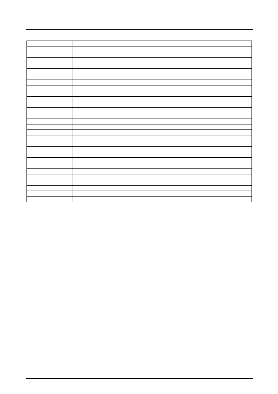
Pin Functions
Pin No.
Symbol
Pin descriptions
1
V
CC
2
Channel 5 power supply
2
V
O
5
Loading output ( )
3
V
O
5
Loading output ( )
4
V
O
4
Channel 4 output ( )
5
V
O
4
Channel 4 output ( )
6
V
O
3
Channel 3 output ( )
7
V
O
3
Channel 3 output ( )
8
V
O
2
Channel 2 output ( )
9
V
O
2
Channel 2 output ( )
10
V
O
1
Channel 1 output ( )
11
V
O
1
Channel 1 output ( )
12
V
CC
1
Channels 1 to 0 4 (BTL) power supply (This pin must be shorted to V
CC
-S)
13
V
IN
1
Channel 1 input
14
V
IN
1G
Channel 1 input (gain adjustment input)
15
V
IN
2
Channel 2 input
16
V
IN
2G
Channel 2 input (gain adjustment input)
17
V
IN
3
Channel 3 input
18
V
IN
3G
Channel 3 input (gain adjustment input)
19
REG-IN
Regulator input (external pnp transistor base)
20
REG-OUT
Regulator output (external pnp transistor collector)
21
VREF-IN
Reference voltage input
22
V
CC
-S
Signal system power supply (This pin must be shorted to V
CC
1.)
23
V
IN
4G
Channel 4 input (gain adjustment input)
24
V
IN
4
Channel 4 input
25
MUTE
Channels 1 to 4 (BTL amplifiers) output on/off control
26
S-GND
Signal system ground
27
FWD
Channel 5 (VLO) output switching (FWD); loading block logic input
28
REV
Channel 5 (VLO) output switching (REV); loading block logic input
Note:
The center frame (FR) is used as the power system ground. Along with the signal system ground (S-GND), this level must be the lowest potential
in the system.
The three power supply pins V
CC
�S, V
CC
1, and V
CC
2 must be shorted together externally.

LA6575H
No.7819-4/8
Pin Functions
Pin No.
Symbol
Pin name
Pin description
Equivalent circuit
13
14
15
16
17
18
23
24
V
IN
Inputs
Inputs
V
IN
G
Vref
V
IN
V
CC
-S
4
5
6
7
8
9
10
11
V
O
Outputs
Outputs
OUT
V
CC
1
25
MUTE
Mute
ON/OFF each output
MUTE: H output ON
MUTE: L output OFF
MUTE
S-GND
100k
VCC-S
100k
2
3
V
O
5
V
O
5
VO5
H bridge outputs
VO5
VO5+
VCC2
Continued on next page

LA6575H
No.7819-5/8
Continued from preceding page.
27
28
FWD
REV
FWD
REV
H bridge inputs
FWD
V
CC
2
H Bridge Block
FWD
REV
VO5
VO5
Mode
L
L
OFF
OFF
Open 1
L
H
H
L
Forward
H
L
L
H
Reverse
H
H
L
L
Brake 2
Note 1: The output are in the high-impedance state in this mode
2: In brake mode, the sink side transistors are on (short-circuit braking). The VLO and VLO levels go to a level essentially the same as the
ground level.
Relationship between the MUTE pin and the power supplies (V
CC
)
CH1
CH2
CH3
CH4
V
CC
1
V
CC
2
MUTE
H Bridge

LA6575H
No.7819-6/8
Block Diagram
MUTE
1
2
3
4
5
15
16
10
11
12
13
14
FR
27
26
22
21
20
19
FR
V
CC
1
V
O
1-
V
O
1+
V
O
2+
V
O
2-
V
O
4-
FWD
REV
V
O
5-
V
O
5+
V
O
3+
V
O
4+
V
IN
3
REG-IN
V
CC
-S
FR
FR
6
7
8
9
17
18
23
24
25
28
V
IN
4G
V
IN
4
V
IN
2G
V
IN
3G
V
O
3-
V
CC
2
REG-OUT
VREF-IN
S-GND
V
IN
2
V
IN
1G
CH2
V
IN
1
Mute
Thermal shutdown
CH3
CH1
Lev
el s
h
i
ft
CH4
CH5
CH1.2.3.4
Power
CH5
Power
MUTE is as follows:
High: Output ON
Low: Output OFF
Signal system power
5 VREG
(External PNPTrE)
22 k 11
k
11 k
11 k
11 k
22 k
22 k
22 k
Lev
el s
h
i
f
t
Lev
el s
h
i
f
t
Lev
el s
h
i
f
t
O
u
tput c
ontr
o
l
Input

LA6575H
No.7819-7/8
Sample Application Circuit
1
2
3
4
5
6
7
V
CC
2
V
O
5
28
27
26
25
24
23
22
21
20
19
18
17
16
15
F
R
8
9
10
11
12
13
14
F
R
V
O
5+
V
O
4+
V
O
4
V
O
3+
V
O
3
V
O
2+
V
O
2
V
O
1+
V
O
1
V
CC
1
V
IN
1
V
IN
1G
V
IN
2
V
IN
2G
V
IN
3
V
IN
3G
REG-IN
REG-OUT
VREF-IN
V
CC
-S
V
IN
4G
V
IN
4
MUTE
S-GND
FWD
REV
M
LOADING
MOTOR
TRACKING
COIL
FOCUS
COIL
M
SPINDLE
MOTOR
M
SLED
MOTOR
REV
FWD
MUTE
TRACKING
SLED
SPINDLE
FOCUS
VREF-IN
V
CC

LA6575H
No.7819-8/8
Specifications of any and all SANYO products described or contained herein stipulate the performance,
characteristics, and functions of the described products in the independent state, and are not guarantees
of the performance, characteristics, and functions of the described products as mounted in the customer's
products or equipment. To verify symptoms and states that cannot be evaluated in an independent
device, the customer should always evaluate and test devices mounted in the customer's products or
equipment.
SANYO Electric Co., Ltd. strives to supply high-quality high-reliability products. However, any and all
semiconductor products fail with some probability. It is possible that these probabilistic failures could give
rise to accidents or events that could endanger human lives, that could give rise to smoke or fire, or that
could cause damage to other property. When designing equipment, adopt safety measures so that these
kinds of accidents or events cannot occur. Such measures include but are not limited to protective circuits
and error prevention circuits for safe design, redundant design, and structural design.
In the event that any or all SANYO products (including technical data, services) described or contained
herein are controlled under any of applicable local export control laws and regulations, such products
must not be exported without obtaining the export license from the authorities concerned in accordance
with the above law.
No part of this publication may be reproduced or transmitted in any form or by any means, electronic or
mechanical, including photocopying and recording, or any information storage or retrieval system, of
otherwise, without the prior written permission of SANYO Electric Co., Ltd.
Any and all information described or contained herein are subject to change without notice due to
product/technology improvement, etc. When designing equipment, refer to the "Delivery Specification" for
the SANYO product that you intend to use.
Information (including circuit diagrams and circuit parameters) herein is for example only; it is not
guaranteed for volume production. SANYO believes information herein is accurate and reliable, but no
guarantees are made or implied regarding its use or any infringements of intellectual property rights or
This catalog provides information as of August, 2004. Specifications and information herein are subject to
change without notice.