 | –≠–ª–µ–∫—Ç—Ä–æ–Ω–Ω—ã–π –∫–æ–º–ø–æ–Ω–µ–Ω—Ç: LA71525M | –°–∫–∞—á–∞—Ç—å:  PDF PDF  ZIP ZIP |
LA71525M
No. 5843-1/25
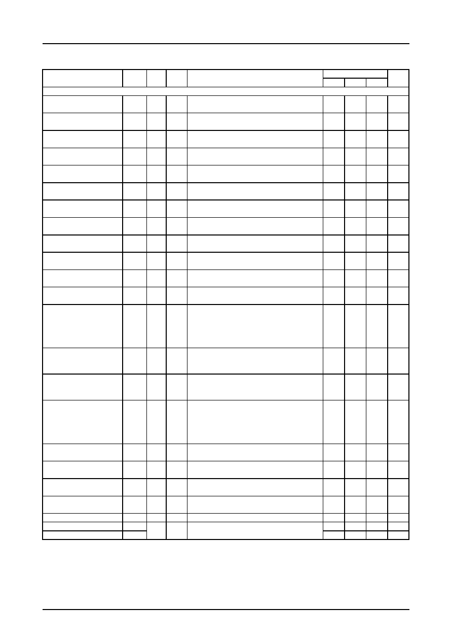
Parameter
Recommended supply voltage
Recommended operating supply
voltage range
Symbol
V
CC
max
V
CC
max
Pd max
Topr
Tstg
Ratings
7.0
9.0
1400
≠10 to +65
≠40 to +150
Parameter
Maximum supply voltage
Allowable power dissipation
Operating temperature
Storage temperature
Ratings
5.0
6.8
(7.5)
4.8 to 5.5
6.4 to 7.9
LA71525M
Video/audio signal processor for VHS VCRs
(single chip for Y/C/A)
Monolithic Linear IC
The LA71525M is a video/audio signal processor IC
for VHS VCRs. It handles recording and playback of
PAL/GBI, MESECAM, and 4.43 NTSC signals.
NTSC software tapes can be converted to PAL for
monitoring, and the IC realizes high picture and sound
quality. The IC requires no adjustments and minimizes
the peripheral component count, making it possible to
implement efficient signal handling at low cost.
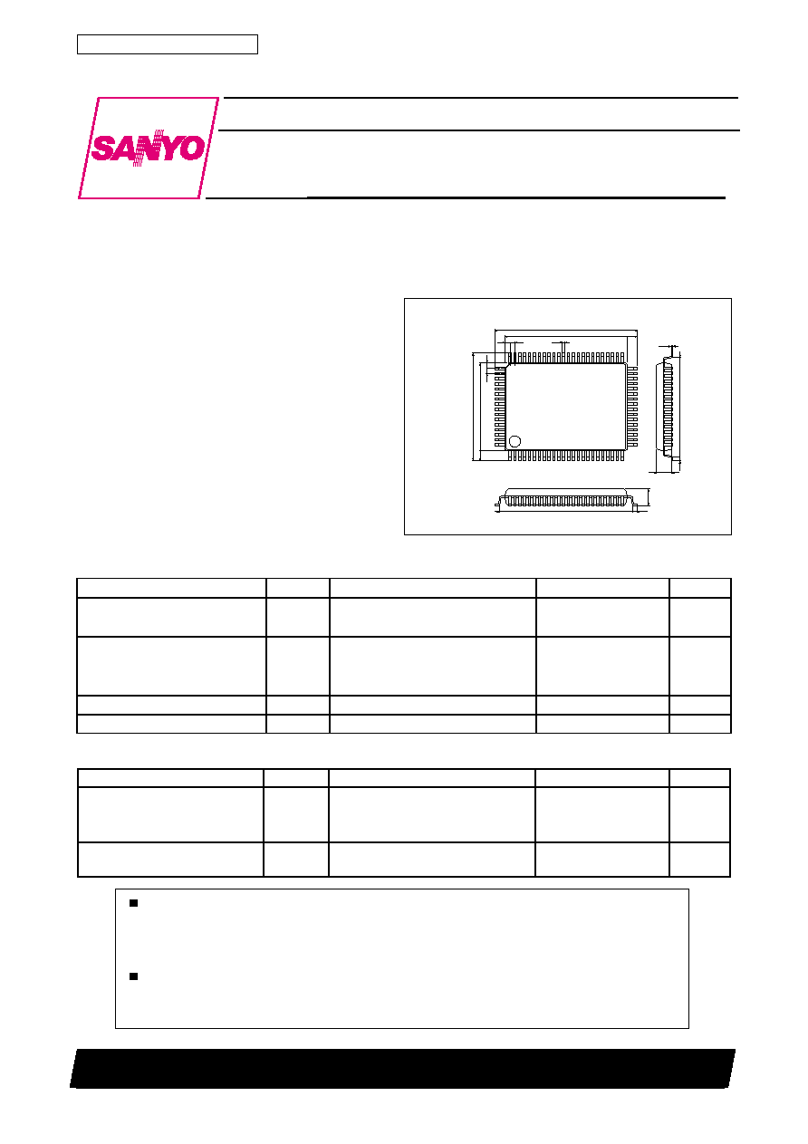
Package Dimensions
unit: mm
3174-QFP80E
[LA71525M]
Overview
SANYO : QFP80E (QIP80E)
Ordering number : EN5843
Maximum Ratings
at Ta = 25
∞
C
Specifications
Operating Conditions
at Ta = 25
∞
C
31799RM(KI)
V
CC
2
V
CC
1
SANYO Electric Co., Ltd. Semiconductor Business Headquarters
TOKYO OFFICE Tokyo Bldg., 1-10, 1 Chome, Ueno, Taito-ku, TOKYO, 110-8534 JAPAN
V
CC
1 opg
V
CC
2 opg
(V
CC
2)
0.15
1.6
14.0
17.2
0.8
1
24
25
40
41
64
65
80
21.6
0.8
3.0max
1.0
2.70
15.6
0.8
1.6
0.35
23.2
20.0
0.8
0.8
Any and all SANYO products described or contained herein do not have specifications that can handle
applications that require extremely high levels of reliability, such as life-support systems, aircraft's
control systems, or other applications whose failure can be reasonably expected to result in serious
physical and/or material damage. Consult with your SANYO representative nearest you before using
any SANYO products described or contained herein in such applications.
SANYO assumes no responsibility for equipment failures that result from using products at values that
exceed, even momentarily, rated values (such as maximum ratings, operating condition ranges, or other
parameters) listed in products specifications of any and all SANYO products described or contained
herein.
Unit
V
V
V
V
V
Unit
V
V
mW
∞C
∞C
Symbol
Conditions
pin 36, 41, 47
pin 76
Ta
65∞C
Conditions
pin 36, 41, 47
pin 76
(pin 76)
114.3 x 76.1 x 1.6 mm
3
with paper
phenol substrate
LA71525M
No. 5843-2/25
Operating Characteristics
at Ta = 25
∞
C, V
CC
= 5V
Continued on next page
Influx current measured at pin 41 in power save mode
Sum of influx current at pins 36, 41, 47, 76 measured;
5V: pins 36, 41, 47; 7V: pin 76
T38 output level measured with
V
IN
= 1.0 Vp-p video signal (PAL)
T38 output level measured with
V
IN
= 1.0 Vp-p video signal (NTSC)
Ratio of V
EE
and T38 output level with
V
IN
= 2.0 Vp-p video signal
Ratio of V
EE
and T38 output level with
V
IN
= 0.5 Vp-p video signal
T38 SYNC level measured with
V
IN
= 700 mVp-pLUMI, 600 mVp-p SYNC
T38 SYNC level measured with
V
IN
= 700 mVp-pLUMI, 150 mVp-p SYNC
T37 output pulse crest value measured with
V
IN
= 1.0 Vp-p video signal
T37 output pulse width measured with
V
IN
= 1.0 Vp-p video signal
Delay of output SYNC vs. input SYNC measured with
V
IN
= 1.0 Vp-p video signal
Input level gradually attenuated and measured when
output pulse width becomes larger than PW
SYR
by 1
µ
s
Potential measured with V
IN
= 1.0 Vp-p video signal,
under following conditions.
T38 sync tip level: L
SYN
Pedestal level: L
PED
White peak level: L
WHT
T38 DC level measured with 2.7V DC applied to T33.
Using this as L
HDR
,
differential to L
PED
(see above) is
calculated.
T38 DC level measured with 1.3V DC applied to T33.
Using this as L
WHR
, differential to L
WHT
(see above) is
calculated.
T25 YNR characteristics measured with
V
IP
= 1 Vp-p standard color bar signal
input
1 MHz response of T25 vs. 500 kHz with V
IN
= 1 Vp-p
standard multiburst signal
2 MHz response of T25 vs. 500 kHz with V
IN
= 1 Vp-p
standard multiburst signal
3 MHz response of T25 vs. 500 kHz with V
IN
= 1 Vp-p
standard multiburst signal
4.43 MHz response of T25 vs. 500 kHz with
V
IN
= 1 Vp-p standard multiburst signal
T18 output level measured in no-signal input condition
T18 output frequency measured in no-signal input
condition
Y
LPF
frequency response
characteristics 1
Y
LPF
frequency response
characteristics 2
Y
LPF
frequency response
characteristics 3
Y
LPF
frequency response
characteristics 4
I
CCS
I
CCR
V
EE
1
V
EE
2
AGC1
AGC2
AGC3
AGC4
V
SYR
PW
SYR
T
SYR
TH
SYR
L
VOR
HDR
R
YNR
WHR
Y
LPF
1
Y
LPF
2
Y
LPF
3
Y
LPF
4
V
FM
F
FM
1
F
FM
2
Serial
00 OFF
10 (weak)
01 (medium)
11 (strong)
min
t y p
max
[REC mode Y]
Current drain
20
22
24
mA
(POWER SAVE MODE)
Current drain
130
145
160
mA
(REC)
EE output level 1
T28A
T38
2.0
2.1
2.2
Vp-p
EE output level 2
T28A
T38
2.0
2.1
2.2
Vp-p
AGC characteristics 1
T28A
T38
0
0.6
1.2
dB
AGC characteristics 2
T28A
T38
≠1.2
≠0.2
0
dB
AGC characteristics 3
T28A
T38
550
650
750 mVp-p
AGC characteristics 4
T28A
T38
370
420
470 mVp-p
Sync separation output level
T28A
T37
4.0
4.2
4.4
Vp-p
Sync separation output pulse
T28A
T37
4.2
4.5
4.8
µ
s
width
Sync separation output
T28A
T37
0.6
0.8
1.0
µ
s
Pre-delay time
Sync separation output
T28A
T37
≠20
≠15
dB
Threshold level
Sync tip level
T28A
T38
700
800
900
mV
Pedestal level
White level measurement
Simulated H insertion level
T28A
T38
≠150
0
mV
White insertion level
T28A
T38
≠150
0
mV
REC YNR operation
T28A
T25
0
0
0
1.7
2.7
3.7
4.2
5.7
7.2
/
/
/
T28A
T25
≠0.3
dB
T28A
T25
≠1.4
≠0.4
dB
T28A
T25
≠4
≠2
0
dB
T28A
T25
≠25
dB
REC-FM output level
T18
304
320
336 mVp-p
Carrier frequency 1 (PAL)
3.725
3.8
3.875
MHz
Carrier frequency 2 (NTSC)
3.325
3.4
3.475
MHz
+0.6
dB
+0.7
+0.2
+150
+150
T18
Parameter
Symbol
Input
Output
Conditions
Unit
Ratings
LA71525M
No. 5843-3/25
min
t y p
max
REC-FM output level
T18
Secondary distortion measured in no-signal input condition
≠40
≠35
dB
Secondary distortion
Deviation 1 (PAL)
T28A
T18
0.95
1.00
1.05
MHz
Deviation 2 (NTSC)
T28A
T18
0.95
1.00
1.05
MHz
FM modulator linearity
T26
T18
Output frequency set to f2.85 with 2.85V DC applied to
≠2
0
%
T26
T18
Output frequency shift
6.5
7.8
9.1
kHz
Emphasis gain
T26A
T24
≠0.75
≠0.25
dB
T37
Detail
T26A
T24
0.1
0.6
1.1
dB
enhancer characteristics 1
Detail
T26A
T24
1.3
2.3
3.3
dB
enhancer characteristics 2
Detail
T26A
T24
1.8
3.3
4.8
dB
enhancer characteristics 3
Nonlinear
T26A
T24
0.3
1.2
2.1
dB
emphasis characteristics 1
Nonlinear
T26A
T24
2.5
3.8
5.0
dB
emphasis characteristics 2
Nonlinear
T26A
T24
6.5
8.0
9.5
emphasis characteristics 3
4.5
6.0
7.5
2.5
4.0
5.5
0 0 0
Main linear
T26A
T37
10.5
11.0
11.5
dB
emphasis characteristics 1
Main linear
T26A
T37
12.5
13.0
13.5
dB
emphasis characteristics 2
White clip level
T28A
T37
185
195
205
176
185
194
Dark clip level
T28A
T37
≠57.5
≠52.5
≠47.5
≠52.0
≠47.0
≠42.0
Video output linearity
T28A
T38
T38 stair levels measured with video signal 1.0 Vp-p
≠0.5
0
dB
(linearity unit, 5 stairs) input. Stair linearity determined by
arithmetic processing.
[PB mode Y]
Current drain PB
5V: pins 36, 41, 47; 7V: pin 76
153
170
187
mA
Sum of influx current at pins 36, 41, 47, 76 measured
Dropout compensation time
T15
T38
T20: 4 MHz, 300 mVp-p sine wave
10.5
12.5
14.5
H
T26A
T26A: revert time for T38 output from when 0.5 Vp-p video
signal T15 input is set to 0
DOC characteristics
T15
T38
T15: 4 MHz, 300 mVp-p sine wave
≠1.5
0
dB
T26A
T26A: 0.5 Vp-p video signal
Input/output response 5H after setting T15 input to 0
PB Y level
T15
T38
Playback Y level with DEV = 1.0 MHz FM signal input
2.00
2.10
2.20
Vp-p
Self-recording/playback Y level
T38
Playback Y level for self-recording/playback
1.93
2.10
2.27
Vp-p
+2
+0.5
+1.5
+0.25
dB
%
%
Parameter
Symbol
Input
Output
Conditions
Ratings
Unit
Continued from preceding page
1/2f
H
carrier shift
Continued on next page
H
MOD
DEV1
L
MOD
DEV2
G
EMP
24
G
EMP
37
CS
G
ENH
2
G
ENH
1
G
ENH
3
G
NLEMP
1
G
NLEMP
2
G
NLEMP
3
G
ME
1
G
ME
2
L
WC
L
DC
LINY
I
CCP
T
DOC
G
DOC
V-Y
OUT
R/P-
OUT
T18 deviation measured with V
IN
= white 100% 1 Vp-p
T18 deviation measured with V
IN
= white 100% 1 Vp-p
Level difference of T26A and T37 measured with
V
IN
= 500 mVp-p, 10 kHz sine wave input
Level difference of T26A and T37 measured with
V
IN
= 158 mVp-p, 2 MHz sine wave input
Differential with G
EMP
24
Level difference of T26A and T24 measured with
V
IN
= 50 mVp-p, 2 MHz sine wave input
Differential with G
EMP
24
Level difference of T26A and T24 measured with
V
IN
= 15.8 mVp-p, 2 MHz sine wave input
Differential with G
EMP
24
Level difference of T26A and T24 measured with
V
IN
= 500 mVp-p, 2 MHz sine wave input
Differential with G
EMP
24
Level difference of T26A and T24 measured with
V
IN
= 158 mVp-p, 2 MHz sine wave input
Differential with G
EMP
24
Level difference of T26A and T24 measured Serial 1
with V
IN
= 50 mVp-p, 2 MHz sine wave input 2
Differential with G
EMP
24 3
4
Level difference of T26A and T37 measured with
V
IN
= 50 mVp-p, 500 kHz sine wave input
Differential with G
EMP
37
Level difference of T26A and T37 measured with
V
IN
= 50 mVp-p, 2 MHz sine wave input
Differential with G
EMP
37
White clip level at T37 measured with CTL 1
V
IN
= white 100% 1.0 Vp-p 2
Dark clip level at T37 measured with CTL 1
V
IN
= white 100% 1.0 Vp-p 2
LA71525M
No. 5843-4/25
Continued on next page
Continued from preceding page
Ratio of T25 4 MHz component and SDEM with
V
IN
= 300 mVp-p f = 4 MHz
V
IN
= white 50% + CW
(15.8 mVp-p)
Ratio of 32 fH component and
32.5 fH component
Input/output response measured with
V
IN
= white 50% + sine wave f = 2 MHz 158 mVp-p
00 OFF
10 (weak)
01 (medium)
11 (strong)
T38 video output sync tip (L
SYN
), pedestal (L
PED
), white
level (L
WHT
) potential measured with V
IN
= white 100%
0.5 Vp-p
DC voltage at T38 is measured when 5V is applied to
T33. Taking this as L
VDP
, differential with L
SYN
above
is calculated.
DC voltage at T38 is measured when 2.7V is applied to
T33. Taking this as L
HDP
, differential with L
PED
above is
calculated.
DC voltage at T38 is measured when 1.3V is applied to
T33. Taking this as L
WHP
, differential with L
WHT
above is
calculated.
Pin 37 output pulse crest value measured with
V
IN
= 0.5 Vp-p video signal
Pin 37 output pulse width measured with
V
IN
= 0.5 Vp-p video signal
Delay of output SYNC vs. input SYNC measured with
V
IN
= 0.5 Vp-p video signal
Pin 17 signal amplitude measured with
V
IN
= 150, 300, 600 mVp-p 4 MHz CW
L
DEM
CL
G
NLDE
1
P
YNR
G
WNC
1
G
WNC
4
G
WNC
3
G
WNC
2
G
WNC
5
G
PH
1
G
PH
2
G
PH
3
L
VOR
VDP
HDP
WHP
P
WSYP
T
SYP
G
PH
4
VF
AGC
V
SYP
G
NLDE
2
Serial
V
REG
L
DEM
=
V
DEM
4
≠ (V
DEM
2
+ V
DEM
6
) /2
V
DEM
6
≠V
DEM
2
x 100
min
t y p
max
FM demodulator linearity
T15
T25
≠3.5
0
%
Carrier leak
T15
T25
≠35
dB
Playback YNR characteristics
T26A
T38
0
0
0
≠3.7
≠3.2
≠2.7
≠9.2
≠8.2
≠7.2
≠13.3
≠11.8
≠10.3
Nonlinear
T26A
T38
≠3.5
≠2.5
≠1.5
dB
deemphasis characteristics 1
Nonlinear
T26A
T38
f = 2 MHz, 50 mVp-p
4.5
6.0
7.5
deemphasis characteristics 2
2
2.5 4.0
5.5
3
0.5 2.0
3.5
4
0
0
0
Double noise
T26A
T38
f = 1.2 MHz, 158 mVp-p, pin 69 open
≠4
≠3
≠2
dB
canceler characteristics 1
Gr2 bit 8/7 = "10", Gr5 bit 1 = "1"
Double noise
T26A
T38
f = 1.2 MHz, 50 mVp-p, pin 69 open
≠16.5
≠15.0
≠13.5
dB
canceler characteristics 2
Gr2 bit 8/7 = "10", Gr5 bit 1 = "1"
Double noise
T26A
T38
f = 1.2 MHz, 15.8 mVp-p, pin 69 open
≠32
≠30
≠28
dB
canceler characteristics 3
Gr2 bit 8/7 = "10", Gr5 bit 1 = "1"
Double noise
T26A
T38
f = 2.5 MHz, 15.8 mVp-p, pin 69 open
≠9
≠8
≠7
dB
canceler characteristics 4
Gr2 bit 8/7 = "10", Gr5 bit 1 = "1"
Double noise
T26A
T38
f = 2.5 MHz, 15.8 mVp-p, pin 69 open
≠17
≠15
≠13
dB
canceler characteristics 5
Gr2 bit 8/7 = "10", Gr5 bit 1 = "1"
PIC-CTL hard response
T26A
T38
f = 1 MHz, 158 mVp-p, Gr5 bit 6/5/4 = "1/0/0"
2.5
3.5
4.5
dB
characteristics 1
PIC-CTL hard response
T26A
T38
f = 2 MHz, 158 mVp-p, Gr5 bit 6/5/4 = "1/0/0"
6
7
8
dB
characteristics 2
PIC-CTL soft response
T26A
T38
f = 1 MHz, 158 mVp-p, Gr5 bit 6/5/4 = "0/0/0"
6
7
8
dB
characteristics 1
PIC-CTL soft response
T26A
T38
f = 2 MHz, 158 mVp-p, Gr5 bit 6/5/4 = "0/0/0"
≠8
≠7
≠6
dB
characteristics 2
Sync tip level
T26A
T38
Pedestal level
≠
≠
≠
White level measurement
Simulated V insertion level
T26A
T38
≠50
0
mV
Simulated H insertion level
T26A
T38
≠100
0
mV
White insertion level
T26A
T38
≠100
0
mV
Sync separation output level
T26A
T37
4.0
4.2
4.4
Vp-p
Sync separation output pulse
T26A
T37
4.35
4.65
4.95
µ
s
width
Sync separation output
T26A
T37
0.7
0.9
1.1
µ
s
Pre-delay time
4V regulator
T26A
T37
T31 DC level measured
3.8
4.0
4.2
V
FMAGC output level
T15
T17
325
350
375 mVp-p
+50
dB
dB
+3.5
+100
+100
CTL 1
Parameter
Symbol
Input
Output
Conditions
Unit
Ratings
LA71525M
No. 5843-5/25
min
t y p
max
[REC mode chroma]
REC chroma
T28A
T14A
215
225
235 mVp-p
low-range converter output level
180
190
200
REC chroma/FM ratio
T28A
T14A
≠3.7
≠3.0
≠2.3
dB
T18
Burst emphasis amount
T28A
T14A
5.5
6.0
6.5
dB
(NTSC mode)
VXO oscillation level
T28A
T56
300
500 700
mVp-p
(PAL mode)
VXO oscillation level
T28A
T56
300 500 700
mVp-p
(NTSC mode)
REC ACC characteristics 1
T28A
T14A
dB
REC ACC characteristics 2
T28A
T14A
≠0.5
≠0.1
dB
REC ACC
T28A
T14A
≠26
dB
Killer input level
REC ACC
T28A
T14A
T14A output level measured with spectrum analyzer and
≠60
≠50
dB
Killer output level
compared to VOR-14, in killer condition as described
above.
REC ACC
T28A
T14A
≠20
dB
Demodulator input level
REC APC
T28A
T14A
Input signal: 50% white signal superimposed with
350
Hz
Pull-in range 1
4.4336 MHz 300 mVp-p CW. After checking that T14A
output is on, CW frequency is raised until T14A output
goes off. Frequency then is gradually reduced.
CW frequency when T14A output goes on: f1
REC APC
T28A
T14A
Same as above, CW frequency is lowered until T14A
≠350
Hz
Pull-in range 2
output goes off. Then frequency is gradually raised.
CW frequency when T14A output goes on: f2
REC AFC
T28A
T51
300 mVp-p, 15.6 kHz pulse train with 5
µ
s pulse width
kHz
Pull-in range 1
is input. Pulse train frequency is raised until T51 output
waveform is impaired. Then frequency is lowered.
Pulse train frequency when T51 waveform becomes
normal: f1
REC AFC
T28A
T51
Same as above, pulse train frequency is lowered until T51
≠1.0
kHz
Pull-in range 2
output waveform is impaired. Then frequency is raised.
Pulse train frequency when T51 waveform becomes
normal: f2
BGP delay time
T28
T37
T37 and T60 waveforms are observed with standard color
3.1
3.4
3.7
µ
s
T60
bar input to T28A
BGP width
4.7
4.9
5.1
µ
s
+0.5
Symbol
Parameter
+0.2
0.5
0.2
+1.0
Input
Output
Conditions
Unit
Ratings
Continued on next page
V
OR
-14
C/FM
G
BE
V
VXO-RP
V
VXO-RN
ACC
R
1
ACC
R
2
V
ACCK-ON
V
OACCK
V
ACCK-OFF
f
APC
1
f
APC
2
f
AFC
2
f
AFC
1
T14A burst level measured with V
IN
= 1 Vp-p CTL 0
standard color bar signal 1
t
D
t
W
Down-converted chroma level/FM level ratio with 100%
chroma input
(R
L
: 5.1 k
)
SP/EP and LP T14A burst level ratio with V
IN
= 1 Vp-p
standard color bar signal
T56 output amplitude measured with FET probe at
V
IN
= 1 Vp-p standard color bar signal
T56 output amplitude measured with FET probe at
V
IN
= 1 Vp-p standard color bar signal
V
IN
= 1 Vp-p standard color bar signal and chroma
signal only boosted by +6 dB
T14A burst level measured and compared to VOR-14
V
IN
= 1 Vp-p standard color bar signal and chroma
signal only boosted by ≠6 dB
T14A burst level measured and compared to VOR-14
T14A input burst level measured when output goes off
and compared to standard input level, with V
IN
= 1 Vp-p
standard color bar signal and chroma signal being
gradually attenuated.
From killer condition as described above, T14A input
burst level is measured when output goes on with input
chroma level being gradually increased. This is
compared to standard input level.
Continued from preceding page
T37
T60
tD tW
A10276
LA71525M
No. 5843-6/25
min
t y p
max
2 fsc output level
T28A
T58
T58 level measured in no-signal input condition
360
400
440 mVp-p
2 fsc duty
T28A
T58
T58 duty measured in no-signal input condition
40
50
60
%
[PB mode chroma chroma]
PB chroma video
T15A
T38
From T15A in PB and SP mode, a chroma signal
490
580 670
mVp-p
Output level
T26A
down-converted from the PAL chroma noise test signal
(PAL mode)
(SP mode, burst 80 mVp-p) and mixed with a 4 MHz
300 mVp-p sine wave is input.
From T26A, a 50% white signal is input.
Burst level is measured at T38.
PB chroma video
T15A
T38
From T15A in PB and SP mode, a chroma signal
490
580 670
mVp-p
Output level
T26A
down-converted from the NTSC chroma noise test signal
(NTSC mode)
(SP mode, burst 160 mVp-p) and mixed with a 4 MHz
300 mVp-p sine wave is input.
From T26A, a 50% white signal is input.
Burst level is measured at T38.
PB chroma
T15A
170 200 230
mVp-p
Pin 46 output level
T26A
T46
T15A
0.5
0.8
dB
T26A
T46
T15A
T46
≠0.5
≠0.2
dB
T26A
PB killer input level
T15A
T46
≠25
dB
T26A
Chroma output level in PPB killer
T15A
T38
≠44
≠40
dB
condition
T26A
PB main converter carrier leak
T15A
T38
≠40
≠33
dB
T26A
Burst deemphasis
T15A
T46
629 kHz, 160 mVp-p CW is mixed with 4 MHz, 300 mVp-p
≠5.75
≠5.50
≠5.25
dB
(NTSC mode)
T26A
CW and input to T15A.
50% white signal is input from T26A.
Output level during T46 burst interval and during other
times is compared.
PB XO output level
T59
T59 output level measured with FET probe in PB mode
300
500
700
mVp-p
(PAL mode)
PB XO oscillator frequency
T59
T59 frequency measured in PB mode: f
≠9
0
Hz
deviation (PAL mode)
NTSC -> PAL conversion
T15A
≠1
0
dB
V axis burst level
T26A
T38
NTSC -> PAL conversion
T15A
≠2
0
dB
Burst level ratio
T26A
T38
Symbol
Parameter
+9
+1
+2
+9
+1
+2
Input
Output
Conditions
Ratings
Unit
Under same conditions as above, +45
∞
burst level is
measured and compared to V
BNAP
Continued from preceding page
Continued on next page
V2
fsc
D2
fsc
P
Vop-38
N
Vop-38
Vop-46
ACC
P
1
ACC
P
2
PB ACC characteristics 1
PB ACC characteristics 2
V
ACK-P
V
OACK-P
C
LP
G
BD
V
XO-PP
V
BNAP
f
XOP
B-NAP
Under same conditions as for P
Vop-38
, T46 burst level is
measured.
Under same conditions as for P
Vop-38
, input chroma
level is raised by +6 dB. T46 burst level is measured
and compared to P
Vop-46
.
Under same conditions as for P
Vop-38
, input chroma
level is raised by ≠6 dB. T46 burst level is measured
and compared to P
Vop-38
.
Under same conditions as for P
Vop-38
, input chroma
level is attenuated and input burst level is measured
when chroma output at T46 goes off (compared to
standard input 80 mVp-p)
T38 measured with spectrum analyzer and compared to
P
Vop-38
in killer condition as described above.
Under same conditions as for P
Vop-38
, T38 is measured
with spectrum analyzer and 4.43 MHz component is
compared to 5.06 MHz component.
From T15A, down-converted chroma noise test signal
mixed with 4 MHz, 300 mVp-p CW is input.
From T26A, 50% white signal is input.
≠45
∞
burst level at T38 is measured and compared to
P
Vop-38
LA71525M
No. 5843-7/25
min
t y p
max
NTSC -> PAL conversion chroma
T15A
4 MHz, 300 mVp-p CW and 100% chroma signal phase
160
180
200
deg
phase
T26A
T38
shifted by ≠90
∞
from burst are mixed and input to T15A.
50% white signal is input to T26A.
Chroma phase when pin 67 is 0V is measured and taken
as
1. Chroma phase when pin 67 is 5V is measured and
taken as
2. P-NAP =
1 ≠
2
[REC mode/EQ]
REC EQ characteristics 1
T22
T18
≠3
≠2
≠1
dB
REC EQ secondary distortion
T22
T18
Under same conditions as above, secondary harmonics
≠40
≠35
dB
are measured.
REC EQ characteristics 2
T22
T18
≠20
dB
REC EQ characteristics 3
T22
T18
≠20
dB
REC EQ characteristics 4
T22
T18
≠3.3
≠2.3
≠1.3
dB
REC EQ characteristics 5
T22
T18
≠1
0
dB
[PB mode/EQ]
PB EQ characteristics 1
T15A
T17
≠2.5
≠1.1
0.0
dB
PB EQ secondary distortion
T15A
T17
Under same conditions as above, secondary harmonics
≠40
≠30
dB
are measured.
PB EQ characteristics 2
T15A
T17
≠30
dB
PB EQ characteristics 3
T15A
T17
7.8 MHz
≠25
dB
PB EQ characteristics 4
T15A
T17
≠30
dB
PB EQ characteristics 5
T15A
T17
≠1
0
dB
PB EQ characteristics 6
T15A
T17
≠11
≠10
≠9
dB
+1
Symbol
Parameter
+1
+1
+1
Input
Output
Conditions
Ratings
Unit
Continued from preceding page
Continued on next page
G
REQ1
H
REQ
G
REQ2
G
REQ3
G
REQ5
G
PEQ1
G
REQ4
H
PEQ
G
PEQ2
G
PEQ3
G
PEQ4
G
PEQ5
G
PEQ6
V
IN
= 500 mVp-p, f = 4 MHz
Input/output response measured
V
IN
= 500 mVp-p, f = 627 kHz
Input/output response measured
V
IN
= 500 mVp-p, f = 1.07 MHz
Input/output response measured
V
IN
= 500 mVp-p, f = 4.5 MHz
Input/output response measured
V
IN
= 500 mVp-p, f = 2.0 MHz
Input/output response measured
V
IN
= 400 mVp-p, f = 4 MHz
Input/output response measured
V
IN
= 400 mVp-p, f = 627 kHz
Input/output response measured
V
IN
= 400 mVp-p
High-range trap frequency and gain measured
V
IN
= 400 mVp-p, f = 1.07 MHz
Input/output response measured
V
IN
= 400 mVp-p, f = 4.5 MHz
Input/output response measured
V
IN
= 400 mVp-p, f = 2.0 MHz
Input/output response measured
P-NAP
LA71525M
No. 5843-8/25
V
GLP
V
GLR
THD
L
V
NOL
V
OML
V
OA
ALC
THD
A
M
PB
M
A
1
M
A
2
M
A
3
VG
OE
V
NIE
VG
R
THD
R
V
OMR
I
CCRA
I
CCPA
V
IN
= ≠30 dBV
V
IN
= ≠30 dBV
V
IN
= ≠30 dBV
V
IN
= ≠66 dBV
V
IN
= ≠20 dBV
V
IN
= ≠20 dBV
Electrical Characteristics of Audio System
: V
CC
= 6.8V
: V
CC
= 7.5V
MT
DCO
: V
CC
= 6.8V
: V
CC
= 7.5V
: V
CC
= 6.8V
: V
CC
= 7.5V
: V
CC
= 6.8V
: V
CC
= 7.5V
V
IN
= ≠28 dBV
V
IN
= ≠28 dBV
min
t y p
max
LINE AMP voltage gain (PB)
T11
T77
23.0
23.5
24.0
dB
LINE AMP voltage gain
T71
T77
23.0
23.5
24.0
dB
(A1, A2, A3)
T73
T75
LINE AMP distortion (PB)
T11
T77
0.01
0.1
0.4
%
LINE AMP
--
T77
Rg = 1 k
, DIN audio filter
≠80.0
≠74.0
≠70.5
dBV
Output noise voltage (PB)
LINE AMP
T11
T77
Output voltage for 1% THD
1.3
1.5 1.7
Maximum output voltage (PB)
1.5
1.7 1.9
Output voltage with
T73
T77
≠7
≠6
≠5
dBV
LINE AMP ALC
LINE AMP ALC effect
T73
T77
T73 input level reduced from ≠28 dBV to ≠8 dBV
0
1
3
dB
LINE AMP ALC distortion
T73
T77
0.01
0.1
0.5
%
MUTE attenuation
T11
T77
≠10 dBV signals applied to all inputs and MUTE enabled.
T71
T73
T75
EQ AMP open circuit voltage gain
T7
T10
58
64
70
dB
EQ AMP input converted noise
--
T10
Rg = 620
, DIN audio filter
0.1
0.8
1.8
µ
Vrms
voltage
REC AMP voltage gain
T79
T1
13.6
14.1
14.6
dB
REC AMP distortion
T79
T1
0.001
0.1
0.4
%
REC AMP
T79
T1
Output voltage for 1% THD
1.3
1.5
1.7
Maximum output voltage
Output voltage for 1% THD
1.5
1.7
1.9
Current drain (REC)
--
--
Influx current measured at pin 76
8.8
11.0
13.2
(no-signal condition)
9.2
11.5
13.8
Current drain (PB)
--
--
Influx current measured at pin 76
7.6
9.5
11.4
(no-signal condition)
8.0
10.0
12.0
DC offset voltage (PB) in MUTE
--
T77
DC offset voltage at pin 77 measured for MUTE ON
0
30
50
mV
condition
(no-signal condition)
Parameter
80
90
dB
80
90
dB
120
Vrms
mA
mA
Vrms
Symbol
Input
Output
Conditions
Unit
Ratings
LA71525M
No. 5843-9/25
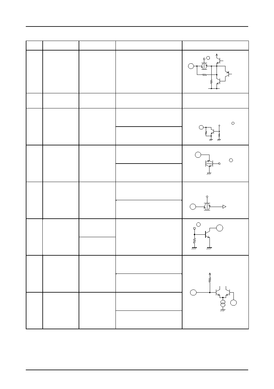
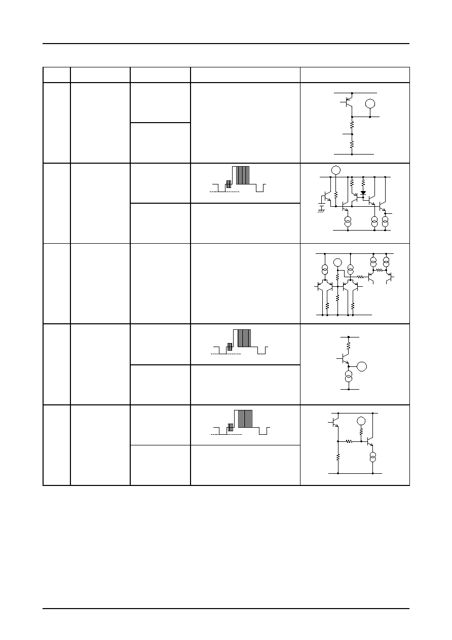
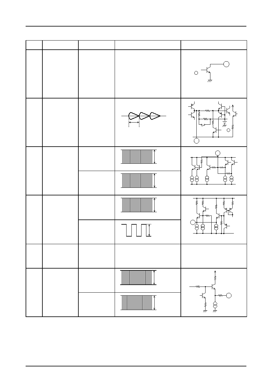
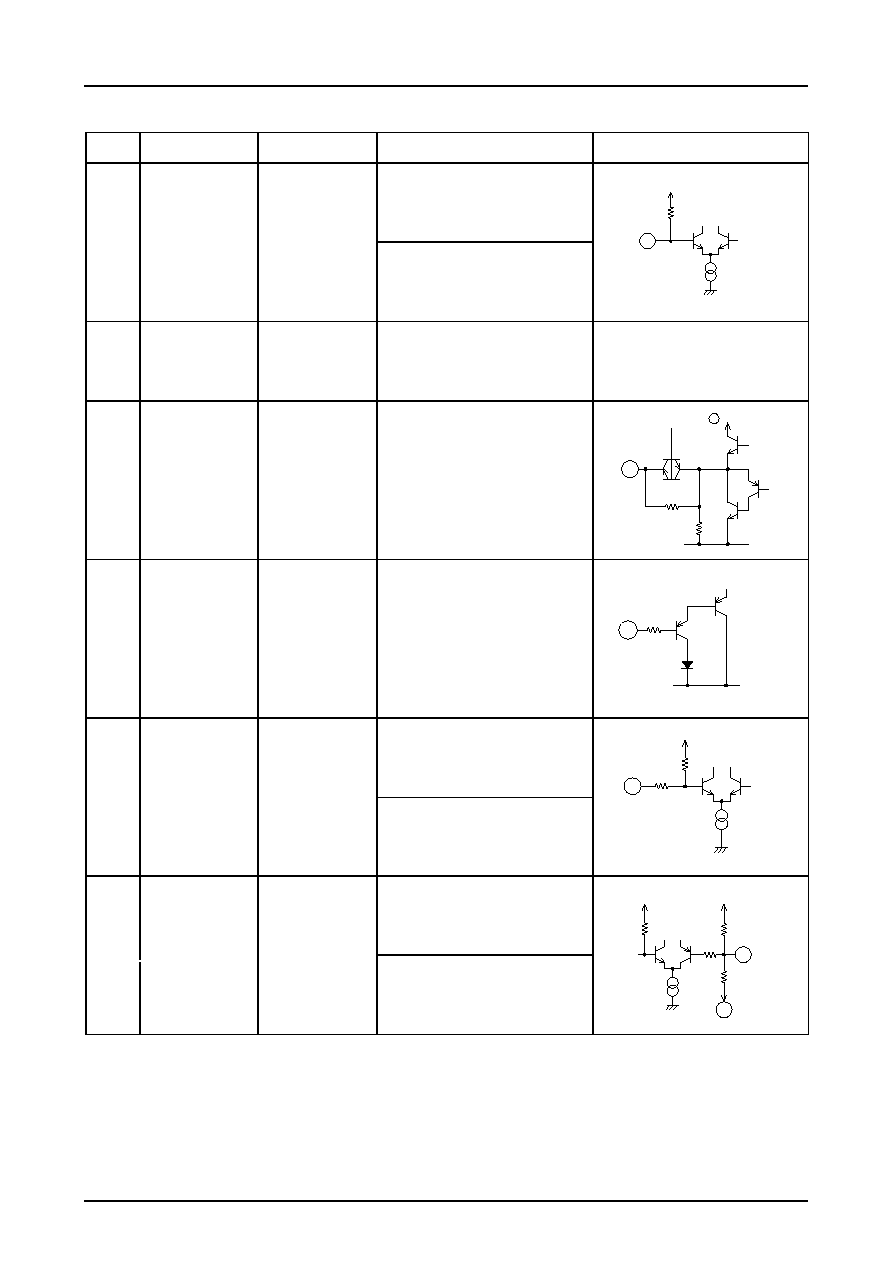
Pin
number
Pin name
Standard DC voltage
Signal waveform
Equivalent circuit
1
A-REC-OUT
3.3V
CW, 3.2 Vp-p
2
A-GND
0V
REC 7V
PB 0V
REC
DC 3.3V
PB
CW, 1 mVp-p
3
A-EQ-SW1
3.3V
4
A-EQ-SW2
A-HEAD
SW-CTL
A-REC-SW
A-EQ-IN
A-EQ-NFB
5
6
7
8
3.3V
3.3V
0V
REC MODE
SP-CW
LP, EP-0V
REC MODE
NONE
REC MODE
NONE
PB, EP MODE
SP, LP-CW
EP-0V
3.3V
PB MODE
CW 1 mVp-p
DC
REC
DC 3.3V
PB
CW, 1 mVp-p
Pin Function
Continued on next page
REC MODE
DC V
REF
1
Power ON/OFF
H
VCC
100k
15k
A10277
3
55k
50k
A10278
H
REC-LP,EP
4
A10279
H
PB-EP
5
A10280
REC
VREF
A10281
6
50k
H
PB
7
8
VREF
120k
100
µ
A
A10282
LA71525M
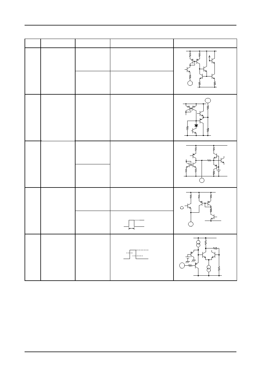
No. 5843-10/25
Continued from preceding page
Continued on next page
A10287
200mVp-p 627kHz
9
10
H
SL/LP
100
µ
A
200
A10283
11
VREF
100
µ
A
120k
500
500
A10284
12
50
µ
A(REC)
200
200
2.3V
1k
1k
1k
200
500
500
500
A10285
13
200
µ
A
2k
1k
50k
200
250
A10286
14
650
µ
A(REC)
200
A10288
Pin
number
Pin name
Standard DC voltage
Signal waveform
Equivalent circuit
REC
DC 3.3V
PB
CW, 95 mVp-p
REC DC 3.3V
PB CW, 95 mVp-p
PB
CW 95 mVp-p
AGC-TC1
REC 2.3V
DC
PB 2.3V
DC
REC 1.8V
PB 1.8V
REC 2.8V
PB 0V
11
A-LINE-PB-IN
3.3V
12
REC-C-OUT
ACC-FILT
13
14
A-EQ-SW1
3.3V
9
10
A-EQ-OUT
3.3V
DC
Carrier Leak
Balancer
REC
DC 3.3V
LA71525M
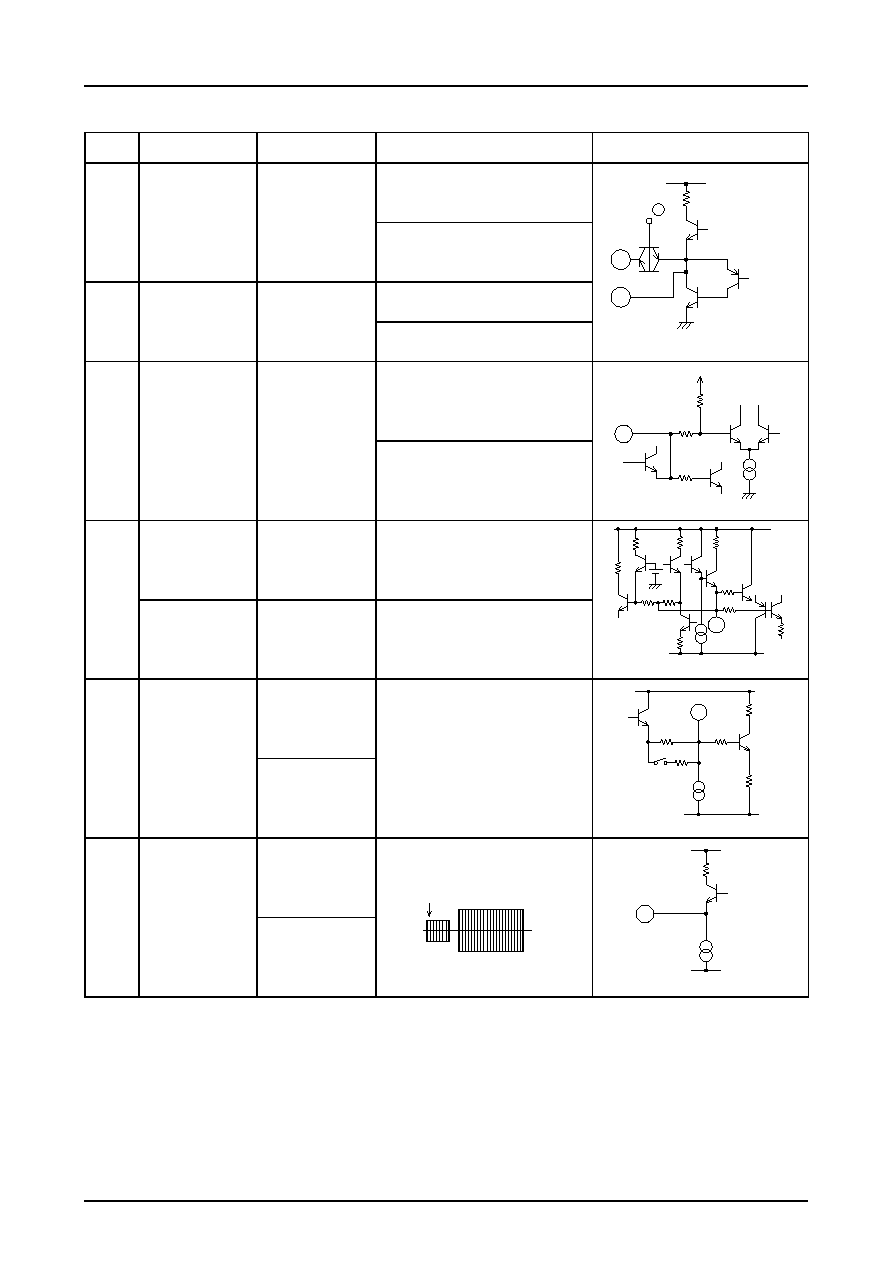
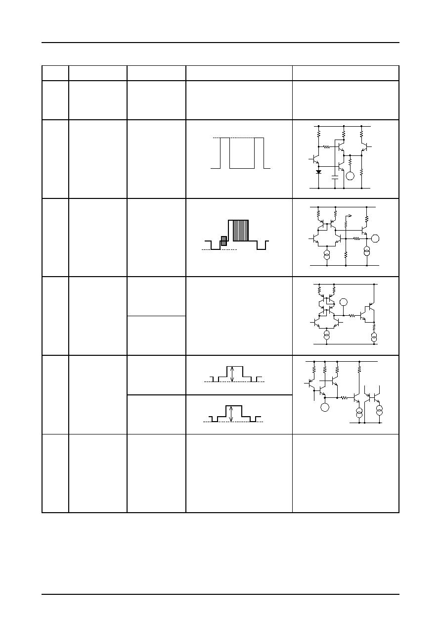
No. 5843-11/25
Pin
number
Pin name
Standard DC voltage
Signal waveform
Equivalent circuit
REC 4.2V
PB 3.2V
REC 1.6V
PB 1.6V
REC 2.6V
FM 730 mVp-p
PB 2.6V
REC 1.9V
PB 1.9V
REC 4.2V
REC PAUSE
2.5V
EE or PB
0V
17
PB-EQ-OUT
REC-Y
FM-OUT
18
REC-H-OUT
19
PB
Y-FM/C-IN
C-IN
(FROM Pre)
PB-Y-FM 400 mVp-p
15
A-EQ-OUT
PB Y-FM 340 mVp-p
DC
PM (R03)
DC
16
PEC Y-FM 730 mVp-p
Continued from preceding page
Continued on next page
A10289
A10292
A10294
15
100
µ
A
500
10k
10k
500
10pF
200
200
3.70V
A10290
1k
300
1k
1k
1k
A10291
16
REG
17
180
µ
A(PB)
A10293
200
100
200
18
A10295
200
100
30k
19
A10296
50k
30k
20k
22k

LA71525M
No. 5843-12/25
Pin
number
Pin name
Standard DC voltage
Signal waveform
Equivalent circuit
REC 4.7V
PB 2.5V
REC 1.6V
PB 1.7V
REC 0V
PB 2.6V
REC 2.1V
PB 0V
REC 2.1V
PB 0V
22
PB-EMITTER
-PEAKING
23
MAIN-EMPH
FILTER
24
PB-Y-FM-IN
(FROM EQ)
PB-Y FM 320 mVp-p
20
DC
AGC-TC2
21
FM 700 mVp-p
DC
DC
MAIN-EMPH
OUT
Continued on next page
Continued from preceding page
A10297
A10300
340mVp-p
A10302
500 mV
2.1V
A10304
00 mVp-p
2.1V
20
100
µ
A(PB)
8k
500
8k
500
A10298
3.25V
21
125
µ
A
A10299
500
200
500
2k
1k
30k
REC-ON
22
A10301
200
200
50k
23
24
A10303
200
500
2k
2k
1k
2pF
23
24
A10305
200
500
2k
2k
1k
2pF
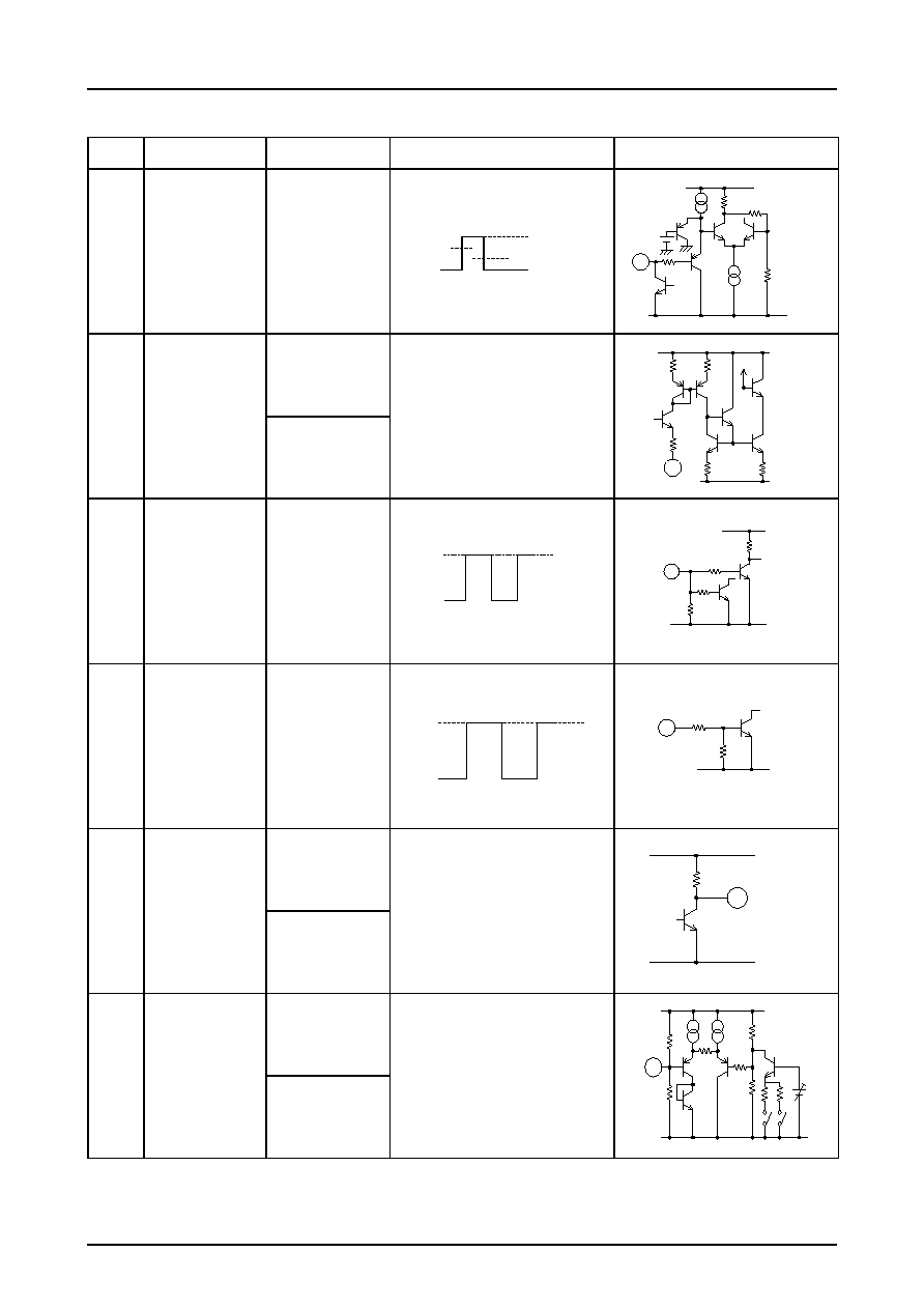
LA71525M
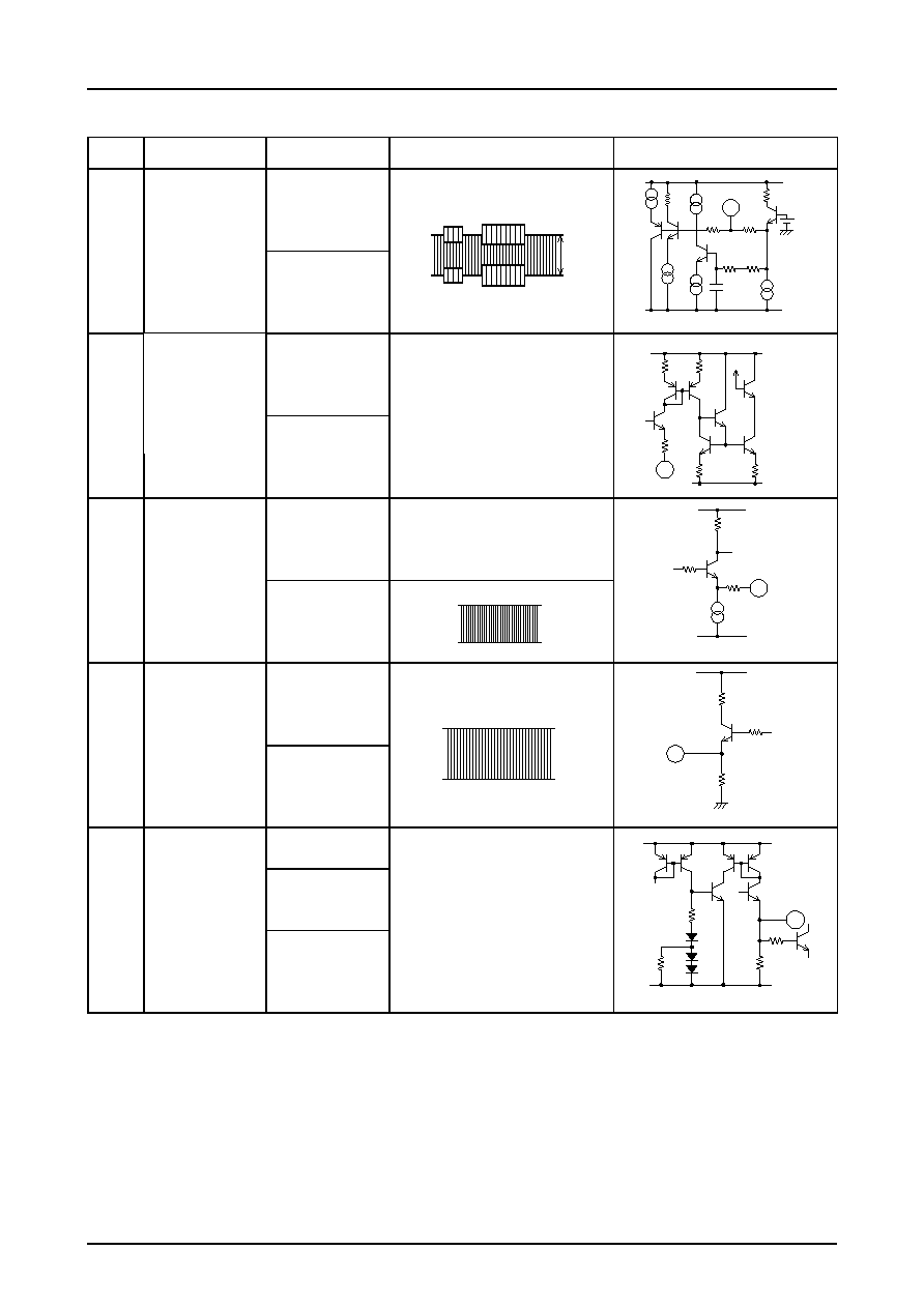
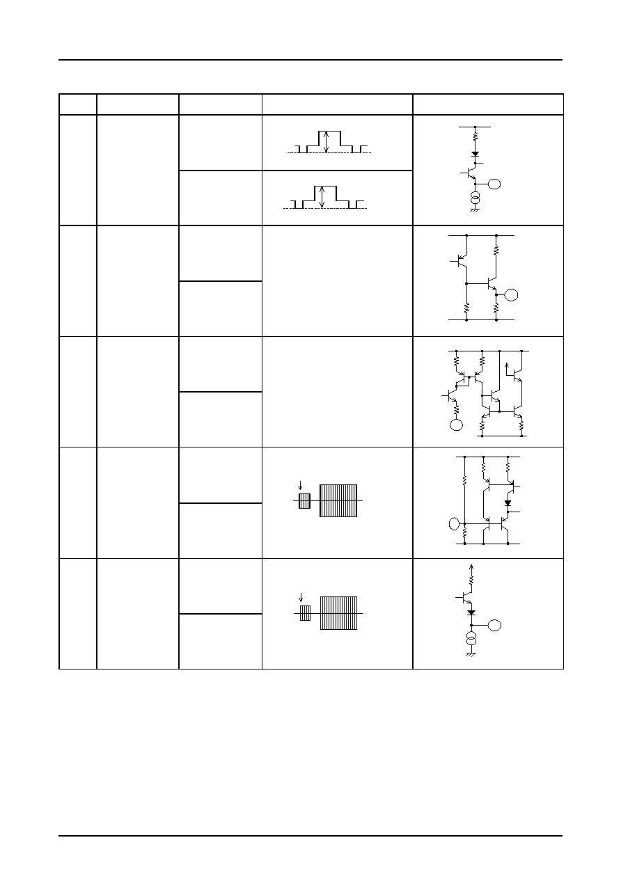
No. 5843-13/25
Pin
number
Pin name
Standard DC voltage
Signal waveform
Equivalent circuit
REC-Y
REC 1.6V
PB 1.2V
REC 2.9V
PB 2.8V
27
Y-GND
0V
PB 0V
DC
REC 2.6V
PB 2.6V
PB 0V
28
VIDEO-IN1
FBC-FILT
(Feed Back Clamp)
29
VIDEO-IN2
30
25
CLAMP-IN
MAIN-DE-EMPH.
OUT
REC
VSYNC 1.7V
26
DC
REC
VSYNC 1.7V
Continued on next page
Continued from preceding page
A10306
500mVp-p
A10307
500mVp-p
A10309
500mVp-p
A10310
500mVp-p
A10312
1.0Vp-p
A10315
1.0Vp-p
25
640
µ
A
200
2.5k
A10308
26
A10311
30k
20k
15k
200
15k
500
400
µ
A
28
A10313
2.3V
200
50k
10k
22
µ
A
24
µ
A
24
µ
A
29
A10314
7.5k
200
20k
500
500
500
130
µ
A
30
A10316
2.3V
200
50k
10k
22
µ
A
24
µ
A
24
µ
A
LA71525M
No. 5843-14/25
Continued from preceding page
0 to 0.8V : Through
1.0 to 2.2V : Character Ins.
2.5 to 3.2V : QH Ins.
3.8 to V
CC
V : QV Ins.
Continued on next page
REC
V
SYNC
1.7V
A10318
1.0Vp-p
A10321
1.0Vp-p
A10323
1.0Vp-p
31
23k
10k
A10317
32
A10319
2.3V
200
50k
10k
22
µ
A
24
µ
A
33
A10320
50
µ
A
50
µ
A
1k
30k
30k
50k
1k
10k
34
A10322
200
470
µ
A
35
A10324
4V
7.5k
7.5k
17k
740
µ
A
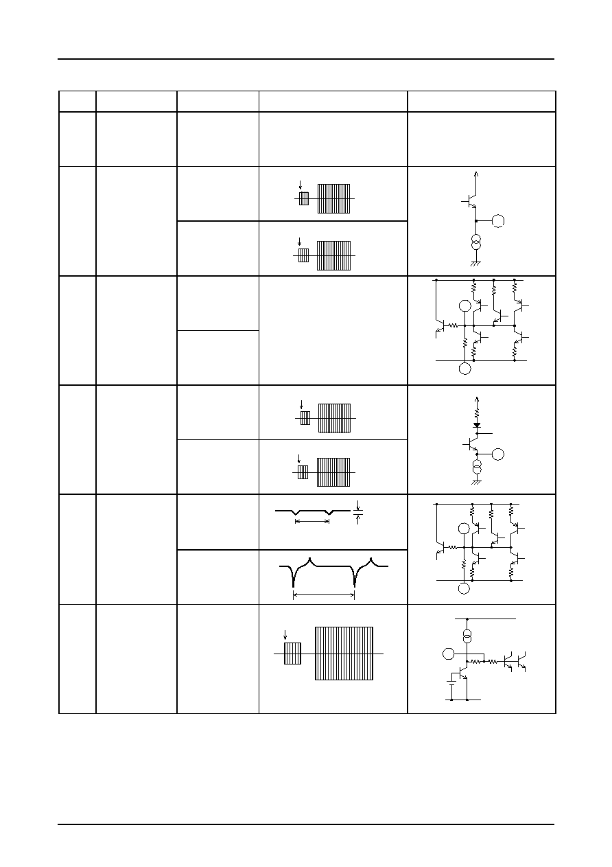
Pin
number
Pin name
Standard DC voltage
Signal waveform
Equivalent circuit
REC 4.1V
PB 4.1V
PB 0V
REC
VSYNC 1.7V
PB 0V
REC 2.3V
PB 3.1V
33
QV/QH-INS
CHARA-INS
VPS-OUT
34
VIDEO-AGC-IN
35
REG
31
VIDEO-IN3
32
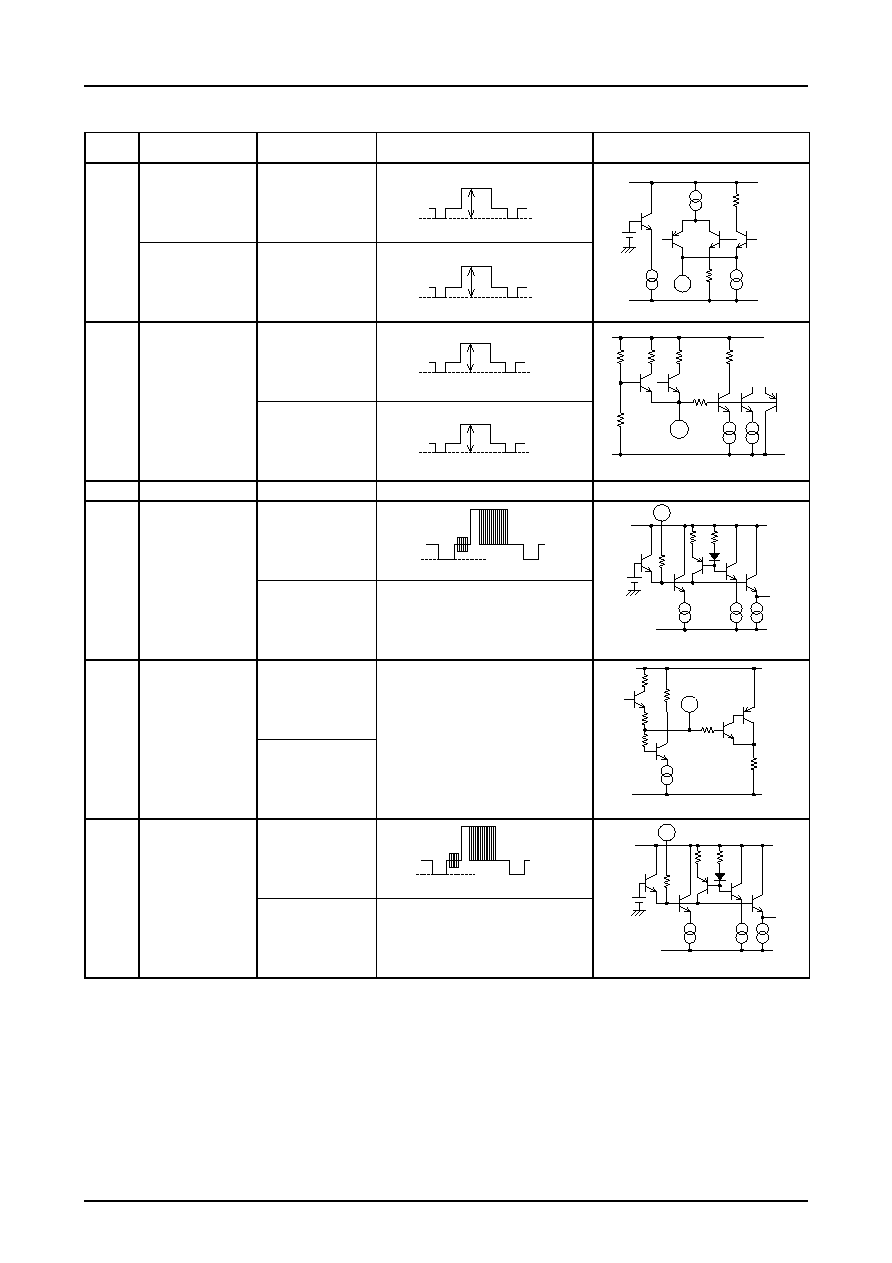
DC
LA71525M
No. 5843-15/25
Pin
number
Pin name
Standard DC voltage
Signal waveform
Equivalent circuit
36
5V
DC
REC 3.1V
PB 3.1V
REC 2.8V
PB 2.8V
39
VCA-FILT
VCA-IN
(CLAMP)
40
41
SYNC-OUT
37
VIDEO-OUT
38
DC
5V
DC
Continued from preceding page
Continued on next page
Y-V
CC
V
SYNC
0.8V
V
CC
2
A10325
4.2V
0V
A10327
2.1Vp-p
A10330
350 mVp-p
A10331
350mVp-p
37
20k
20k
500
500
200
50k
10pF
A10326
38
REG
A10328
100
100
620
µ
A
1.8
µ
A
26k
15.5k
200
11k
39
A10329
200
µ
A
500
9k
1k
1k
40
A10332
1k
15k
15k
200
500
100
µ
A
LA71525M
No. 5843-16/25
Pin
number
Pin name
Standard DC voltage
Signal waveform
Equivalent circuit
REC 1.8V
PB 1.8V
REC 1.7V
PB 1.8V
REC 1.8V
PB 1.9V
REC 0V
PB 2.0V
44
PQ 2 (RO2)
PB CHROMA IN
45
PB CHROMA
OUT
46
Y-CCD-DRIVE
42
NTSC-H OUT
43
DC
NTSC MODE
4.2V
WITHOUT
NTSC MODE
0V
DC
Continued from preceding page
Continued on next page
A10333
350mVp-p
A10334
370mVp-p
A10338
210mVp-p
A10340
210mVp-p
42
350
370
µ
A
A10335
43
200
50k
50k
A10336
44
1k
300
1k
1k
1k
REG
A10337
45
1k
4k
65k
35k
A10339
46
100
400
µ
A
(PB)
A10341
LA71525M
No. 5843-17/25
Pin
number
Pin name
Standard DC voltage
Signal waveform
Equivalent circuit
47
5V
DC
REC 2.8V
PB 2.8V
REC 4.0V
PB 4.1V
REC 2.9V
PB 2.9V
REC 4.0V
PB 4.0V
50
C-CCD-DRIVE 1
AFC/APC-FILT
51
C-CCD-IN
52
C-CCD-DRIVE2
48
SLD-FILT
49
3.2V
DC
Continued from preceding page
Continued on next page
C-V
CC
A10342
150mVp-p
A10343
130mVp-p
A10346
150mVp-p
A10347
130mVp-p
10mVp-p
H
A10349
A10350
Field
A10352
140mVp-p
48
440
µ
A
(PB)
A10344
51
49
500
1k
22k
200
200
A10345
500
2k
50
250
440
µ
A
A10348
51
49
500k
2k
22k
200
200
A10351
500k
1k
52
500
10k
2.5V
97
µ
A
A10353
LA71525M
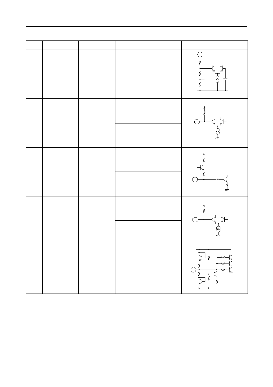
No. 5843-18/25
Pin
number
Pin name
Standard DC voltage
Signal waveform
Equivalent circuit
REC 4.0V
PB 3.9V
REC 2.5V
PB 2.5V
57
C-GND
0V
DC
REC 1.5V
PB 2.8V
55
VXO/XO-IN
56
2 fsc/PB-H
OUT
58
PA STOP-TR-SW
53
REC-APC-FILTER
54
0V
DC
2.1V
VXO/XO-OUT
Continued on next page
Continued from preceding page
A10355
H
A10358
600mVp-p
A10358
600mVp-p
A10360
600mVp-p
500mVp-p
A10361
A10363
400mVp-p
A10364
400mVp-p
53
H
P.A.STOP
A10354
54
H
3rd
2.1V
5k
70k
50k
50k
A10356
55
2k
500
200
62
µ
A
(VXO)
90
µ
A
650
µ
A
(XO)
340
µ
A
(VXO)
200
A10359
56
2k
100k
300k
900
200
100
100
900
µ
A
(XO)
100
µ
A
(XO)
500
µ
A
A10362
A10365
58
200
500
5k
200
LA71525M
No. 5843-19/25
Pin
number
Pin name
Standard DC voltage
Signal waveform
Equivalent circuit
REC 1.5V
DC
PB 1.5V
DC
Color 2.0V
killer 3.0V
61
KILL-FILT
ACK/SLD OUT
62
SERIAL-
CLOCK-IN
63
RL
(RO4)
59
BGP-OUT
60
ACK-OUT
MODE
SLD-OUT
MODE
DC
SYNC+BGP
SYNC 1.4V (typ)
BGP 4.0V or MORE
KILLER MODE 4V or MORE
COLOR MODE 0V
Continued from preceding page
Continued on next page
1H
0
µ
A
200
µ
A
A10369
0V
5V
A10371
1.6V
3.0V
1k
300
1k
1k
1k
A10366
59
REG
200
20k
50k
A10367
60
5k
1k
1.66k
1k
2.5V
A10368
61
200
260
2k
20k
2k
200
A10370
62
H
KIL
SLD
PULSE
50
µ
A
15k
25k
60k
300
3V
A10372
63
LA71525M
No. 5843-20/25
Pin
number
Pin name
Standard DC voltage
Signal waveform
Equivalent circuit
REC 1.6V
PB 1.6V
REC 2.1V
PB 2.1V
66
PAL-PULSE
68
NC-CTL
69
SERIAL-
DATA-IN
64
PQ1
(RO1)
65
67
C-ROTARY-
PULSE-IN
CSC-PULSE-IN
DC
DC
+45
∞
4V or MORE
+45
∞
1V or LESS
Continued on next page
Continued from preceding page
0V
5V
A10373
1.5V
3.0V
A10376
0.8V
0
A10378
0.8V
0
64
ACK
50
µ
A
3V
300
15k
25k
60k
A10374
1k
300
1k
1k
1k
A10375
65
REG
66
85k
20k
1k
1k
A10377
67
1k
20k
A10379
50k
A10380
68
40k
40k
2.2k
17k
500
23k
A10381
69
LA71525M
No. 5843-21/25
Pin
number
Pin name
Standard DC voltage
Signal waveform
Equivalent circuit
REC CW, 95 mVp-p
PB DC 3.3V
REC: ADAPTIVE
PB DC 0V
REC CW, 95 mVp-p
PB DC 3.3V
72
A-ALC-DET
74
A-MUTE-
ON/OFF
70
A-LINE-IN1
71
MUTE
3V or MORE
73
3.3V
0V
3.3V
3.3V
DC
A-LINE-IN2
DC
Continued on next page
Continued from preceding page
A-V
REF-
FILTER
70
GND
2.5V
10k
45k
45k
100
µ
A
A10382
71
VREF
120k
100
µ
A
A10383
72
VCC
200
150
10k
2k
A10384
73
VREF
120k
100
µ
A
A10385
74
VCC
GND
43k
24k
22k
39k
100k
500
500
500
A10386
LA71525M
No. 5843-22/25
Pin
number
Pin name
Standard DC voltage
Signal waveform
Equivalent circuit
REC CW, 95 mVp-p
PB DC 3.3V
76
7V
DC
REC CW, 745 mVp-p
PB DC 3.3V
REC CW 745 mVp-p
PB DC 3.3V
77
A-LINE-OUT
A-LINE-IN3
75
A-ALC DET-IN
3.3V
78
3.3V
CW, 1.4 Vp-p
0V
CW, 1.0 Vp-p
79
80
A-REC-IN
A-REC-NFB
3.3V
3.3V
Continued from preceding page
A-V
CC
75
VREF
120k
100
µ
A
A10387
A10388
77
Power ON/OFF
H
VCC
75k
10k
A10389
500
78
79
VREF
120k
500
100
µ
A
A10390
80
1
VREF
VREF
120k
1.8k
7.3k
500
100
µ
A
A10391
LA71525M
No. 5843-23/25
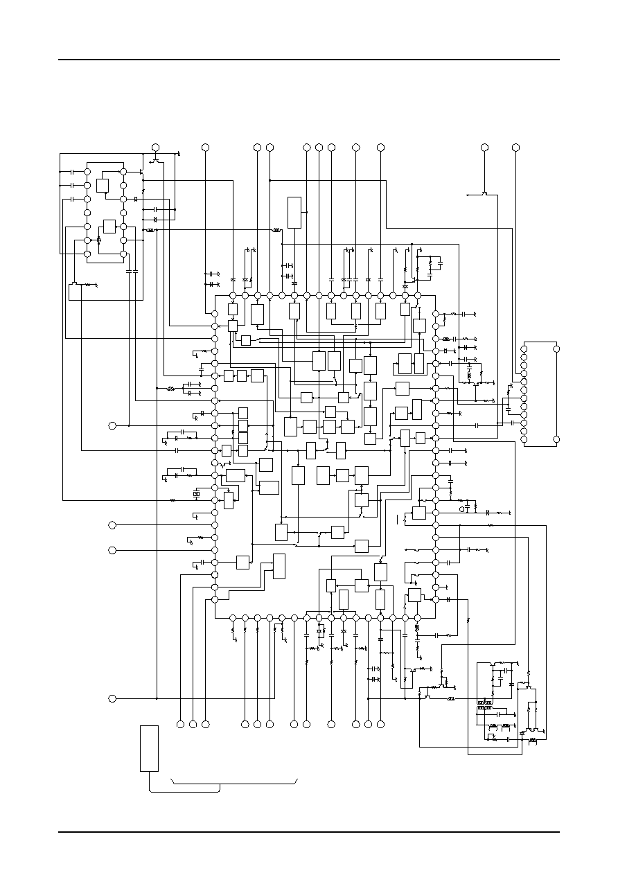
Block Diagram and Sample Application Circuit
1
2
3
4
5
6
7
8
9
10
11
12
13
14
15
16
17
18
19
20
21
22
10
23
24
25
26
27
28
29
30
31
32
33
34
35
36
37
38
39
40
41
1
42
43
44
45
46
47
48
49
50
51
52
53
54
55
56
57
58
59
60
61
62
63
64
65
66
67
68
69
70
71
72
73
74
75
76
77
78
79
80
REC
AMP
KIL
DET
AFC
DET
YC
MIX
AGC
DET
PIC
CTL
DHP
NC
N.L.
DE-EM
EQ
AMP
FM
AGC
REC
APC
DET
PB
APC
DET
ALC
DET
ALC
LINE
AMP
MUTE
SERIAL
DECODER
PB
BGA-A
AMP
V
REF
REC
EQ
SUB
LPF
DOUBLE
LIMIT
DEMOD
ACC
DET
ACC
AMP
MAIN
CONV
MAIN
EMPH
N.L.
EMPH
DETAIL
EMPH
SYNC
SEPA
QV/QH
INS
SUB
CONV
PB
BGA-B
SUB
BPF
REC
BGA
VXO1
BPF1
BPF2
C-LPF
KIL
LPF
VCO
INV
SLD
KIL
B.D.
BPF
NAP
P
P
R
R
CNC
LPF
CLP
1H/2H
DL
1H
DL
VIDEO
AMP
VIDEO
AGC
CLAMP
CLAMP
CLAMP
CLP
YNR
PB-EQ
REC
HD
SW
A-GND
REC-EP.LP
PB-EP
REC
REC
R
P
P
R
P
R
COMB
TH
P
R
P
R.A
B
P
P
R
R
PB-LP.SP
BAL
TC1
PM
PEAKING
MAIN
EMPH
REC H
REC C IN
REC FM IN
PB YC OUT
C SYNC IN
HSWP IN
TRICK H
REC
HIGH
OUT
R
RP
P
P
P
R
R
P
Y-GND
REG
PHASE COMPENSATION
PB-L
Y-V
CC
V
CC
2
PQ2
V
SS
V
DD
N.C.
N.C.
NT:H
3FSC
OUT
CLK
IN
C-V
CC
C-GND
RL
2FSC/PB-H
BGP
ACK
OUT
C-ROT
IN
PQ1
CSOP IN
PAL-PULSE
NC-CTL
MUTE
CTL
A-V
CC
9
8
LA70010 4HD AMP
7
6
5
4
3
2
1
24
11
12
13
+
+
+
+
+
+
+
+
+
+
+
+
+
+
+
+
4.7 k
1 k
1.3 k
1
µ
F
0.1
µ
F
VIDEO IN2
VIDEO IN1
0.1
µ
F
VIDEO IN3
0.1
µ
F
QV.QH.CHARA.IN
VPS OUT
SUB TITLE
DECODER
C-SYNC OUT
VIDEO OUT
200 pF
56 pF
1
µ
F
47
µ
F
10
µ
F
0.1
µ
F
22
µ
F
6.8 k
4.7
µ
F
13 k
2.2 M
82 k
51 k
51 k
8.2 k
12 k
0.01
µ
F
2.2 k
0.047
µ
F
0.022
µ
F
0.1
µ
F
0.022
µ
F
1 k
0.01
µ
F
0.01
µ
F
0.01
µ
F
22
µ
F
47
µ
H
10
µ
F
3.3k
2.7 k
390
390
820
680
33 pF
120
µ
H
390 pF
43 pF
1
µ
F
330 k
M
10
180
22
µ
F
+
47
µ
F
0.1
µ
F
0.01
µ
F
0.01
µ
F
47
µ
F
10
µ
F
100
µ
H
100
µ
H
0.1
µ
F
0.01
µ
F
0.01
µ
F
1
µ
F
0.1
µ
F
47
µ
F
1
µ
F
0.022
µ
F
1.2 k
1
µ
F
100
µ
H
0.01
µ
F
0.047
µ
F
1.8 k
4.43
0.047
µ
F
0.01
µ
F
0.1
µ
F
+
10
µ
F
1 M
1 k
+
8.2 k
1
µ
F
+
+
+
0.1
µ
F
33
µ
F
6.8 k
82 k
0.1
µ
F
6.8 k
82 k
0.1
µ
F
15 k
1.8 k
3.3 k
10 k
22 k
1 k
1 k
2SA1318
2SC3331
2SC3331
R/P
220 pF
AE
FE
2SC3331
2
3
4
5
6
7
14
13
12
11
10
9
8
LC89980
TO/FROM
MI-COM.SERVO
A10392
2 1
3
FBC
MOD
1/2
+
0.01
µ
F
10
µ
F
+
47
µ
F
0.1
µ
F
+
0.1
µ
F
REC SECAM
CHROMA IN
H.SW.P.IN
V
CC
2(+5V)
(POWER SAVE MODE)
PB SECAM
CHROMA IN
CHROMA OUT
SECAM DET
2FSC/PB-H
OUT
BGP OUT
ACK OUT
SERIAL CLOCK IN
SERIAL DATA IN
C-ROT IN
COLOR SEQUENCIAL
COMPENSATOR PULSE IN
PAL-PULSE
OUT
MUTE CTL
AUDIO
IN1
AUDIO
IN2
AUDIO
IN3
VCC+7V
LINE OUT
V
CC
(+5V)
LA71525M
No. 5843-24/25
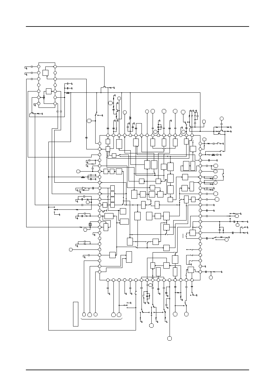
Test Circuit Diagram
1
2
3
4
5
6
7
8
9
10
11
12
13
14
15
16
17
18
19
20
21
22
23
24
25
26
27
28
29
30
31
32
33
34
35
36
37
38
39
40
41
1
42
43
44
45
46
47
48
49
50
51
52
53
54
55
56
57
58
59
60
61
62
63
64
65
66
67
68
69
70
71
72
73
74
75
76
77
78
79
80
REC
AMP
KIL
DET
AFC
DET
YC
MIX
AGC
DET
PIC
CTL
DHP
NC
N.L.
DE-EM
EQ
AMP
FM
AGC
REC
APC
DET
PB
APC
DET
ALC
DET
ALC
LINE
AMP
MUTE
SERIAL
DECODER
PB
BGA-A
AMP
V
REF
REC
EQ
SUB
LPF
DOUBLE
LIMIT
DEMOD
ACC
DET
ACC
AMP
MAIN
CONV
MAIN
EMPH
N.L.
EMPH
DETAIL
EMPH
SYNC
SEPA
QV/QH
INS
SUB
CONV
PB
BGA-B
SUB
BPF
REC
BGA
VXO1
BPF1
BPF2
C-LPF
KIL
LPF
VCO
INV
SLD
KIL
B.D.
BPF
NAP
P
P
R
R
CNC
LPF
CLP
1H/2H
DL
1H
DL
VIDEO
AMP
VIDEO
AGC
CLAMP
CLAMP
CLAMP
CLP
YNR
PB-EQ
REC
HD
SW
A-GND
REC-EP.LP
PB-EP
REC
REC
R
P
P
R
P
R
COMB
TH
P
R
P
R.A
B
P
P
R
R
PB-LP.SP
BAL
TC1
PM
REC-H
OUT
MAIN
EMPH
PEAKING
REC
HIGH
OUT
PM-IN
PM-OUT
R
RP
P
P
P
R
R
P
Y-GND
REG
VIDEO-IN1
SYNC-OUT
VIDEO-OUT
Y-V
CC
V
CC
2
PQ2
V
SS
V
DD
N.C.
N.C.
NT:H
3FSC
OUT
CLK
IN
C-V
CC
C-GND
RL
2FSC/PB-H
BGP
ACK
OUT
C-ROT
IN
PQ1
CSOP IN
PAL-PULSE
NC-CTL
ACK/SLD OUT
SERIAL CLOCK IN
SERIAL DATA IN
C-ROT IN
H.SW.P IN
MUTE
CTL
A-V
CC
+
+
+
+
+
+
+
+
+
+
+
+
+
+
+
T7A
T10A
T11A
T14A
T1A
T15A
T20A
T26A
T17
T18
T19
T23
T24
T46
T62
T72
T66A
T73A
T67A
T63A
T64
T51
T25
T26
T28A
T37
T38
+
T31
T38A
V
CC
1
+
+
+
+
+
+
T77A
V
CC
2
T79A
4.7 k
1.3 k
SW26
1
µ
F
0.1
µ
F
VIDEO-IN2
T30A
0.1
µ
F
VIDEO-IN3
T32A
0.1
µ
F
QVQH INS
T33
200 pF
56 pF
1
µ
F
47
µ
F
1
µ
F
0.1
µ
F
0.1
µ
F
0.1
µ
F
4.7
µ
F
0.1
µ
F
4.7
µ
F
15 k
13 k
SW79
2
1
0.1
µ
F
33
µ
F
SW70
SW72
22
µ
F
2.2 M
1 k
1 k
1 k
7V
SW71
SW75
SW73B
SW73A
2
1
2
1
1
2
2
1
3
12 k
0.01
µ
F
2.7 k
4.7
µ
F
0.047
µ
F
0.1
µ
F
0.022
µ
F
0.022
µ
F
0.01
µ
F
0.01
µ
F
22
µ
F
3.3 k
680
43 pF
120
µ
H
390 pF
1 k
10 k
1 k
39 k
0.01
µ
F
39 k
1 k
2.2 k
1
µ
F
330 k
12
2
1
3
SW8
SW24
SW49
SW22
SW7
SW11
2
13
SW67
SW51
SW20
18 k
620
4.7 k
1 k
330
10
µ
F
+
10
µ
F
0.1
µ
F
47
µ
F
100
µ
H
10
µ
F
1.0M
470
µ
F
51
75
2.2 K
0.1
µ
F
0.01
µ
F
0.01
µ
F
47
µ
F
100
µ
H
0.1
µ
F
0.01
µ
F
0.01
µ
F
75
1
µ
F
0.022
µ
F
0.01
µ
F
2.2 k
47
µ
F
1
µ
F
0.022
µ
F
1.8 k
1 k
10 k
1
µ
F
100
µ
H
0.01
µ
F
0.047
µ
F
8.2 k
1.8 k
4.43 PAL
1
µ
F
0.047
µ
F
0.022
µ
F
1
µ
F
0.1
µ
F
1
2
SW41
5V
1
2
21
3
1 k
+
T56
T60
0.01
µ
F
0.01
µ
F
+
10
µ
F
SW80
1
2
2
3
4
5
6
7
14
13
12
11
10
9
8
LC89980
TO/FROM MI-COM.SERVO
A10393
2 1
3
FBC
MOD
1/2
LA71525M
No. 5843-25/25
This catalog provides information as of March, 1999. Specifications and information herein are subject to change
without notice.
PS
Specifications of any and all SANYO products described or contained herein stipulate the performance,
characteristics, and functions of the described products in the independent state, and are not guarantees
of the performance, characteristics, and functions of the described products as mounted in the customer's
products or equipment. To verify symptoms and states that cannot be evaluated in an independent device,
the customer should always evaluate and test devices mounted in the customer's products or equipment.
SANYO Electric Co., Ltd. strives to supply high-quality high-reliability products. However, any and all
semiconductor products fail with some probability. It is possible that these probabilistic failures could
give rise to accidents or events that could endanger human lives, that could give rise to smoke or fire,
or that could cause damage to other property. When designing equipment, adopt safety measures so
that these kinds of accidents or events cannot occur. Such measures include but are not limited to protective
circuits and error prevention circuits for safe design, redundant design, and structural design.
In the event that any or all SANYO products(including technical data,services) described or
contained herein are controlled under any of applicable local export control laws and regulations,
such products must not be exported without obtaining the export license from the authorities
concerned in accordance with the above law.
No part of this publication may be reproduced or transmitted in any form or by any means, electronic or
mechanical, including photocopying and recording, or any information storage or retrieval system,
or otherwise, without the prior written permission of SANYO Electric Co. , Ltd.
Any and all information described or contained herein are subject to change without notice due to
product/technology improvement, etc. When designing equipment, refer to the "Delivery Specification"
for the SANYO product that you intend to use.
Information (including circuit diagrams and circuit parameters) herein is for example only ; it is not
guaranteed for volume production. SANYO believes information herein is accurate and reliable, but
no guarantees are made or implied regarding its use or any infringements of intellectual property rights
or other rights of third parties.