Overview
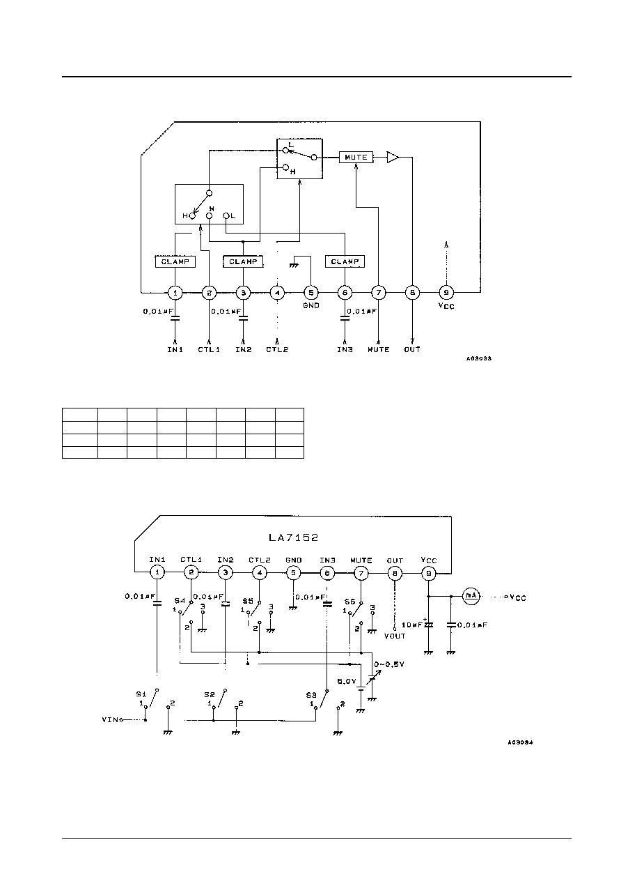
The LA7152 is a three-input (clamped input) single-output
analog switch for video signals. The LA7152 high input
impedance structure allows 0.01 µF ceramic capacitors to
be used as the input coupling capacitors.
Features
∑ Three inputs - one output
∑ Built-in video clamping circuits
∑ Built-in muting function
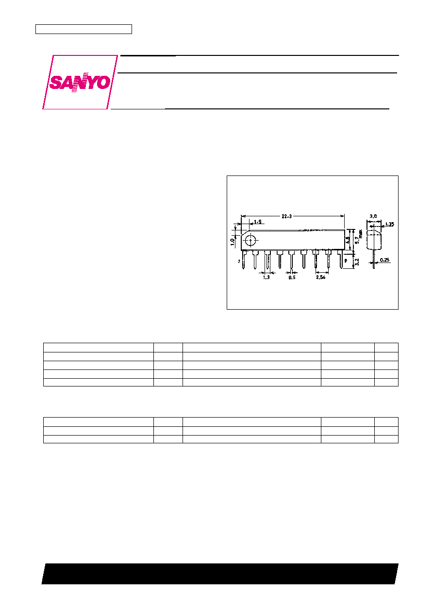
Package Dimensions
unit: mm
3017C-SIP9
Specifications
Maximum Ratings
at Ta = 25∞C
Recommended Conditions
at Ta = 25∞C
Ordering number : EN4955
21095TH (OT) No. 4955-1/5
SANYO: SIP9
[LA7152]
LA7152
SANYO Electric Co.,Ltd. Semiconductor Bussiness Headquarters
TOKYO OFFICE Tokyo Bldg., 1-10, 1 Chome, Ueno, Taito-ku, TOKYO, 110-8534 JAPAN
VCR Electronic Switch
Monolithic Linear IC
Parameter
Symbol
Conditions
Ratings
Unit
Maximum supply voltage
V
CC
max
7.0
V
Allowable power dissipation
Pd max
100
mW
Operating temperature
Topr
≠10 to +70
∞C
Storage temperature
Tstg
≠40 to +150
∞C
Parameter
Symbol
Conditions
Ratings
Unit
Recommended supply voltage
V
CC
5.0
V
Operating supply voltage range
Vopg
4.5 to 6.0
V
Operating Characteristics
at Ta = 25∞C, V
CC
= 5 V
Note: 1. Current drain
S1 = S2 = S3 = 2, S4 = S5 = S6 = 3
2. Maximum input level (input C = 10 µF)
S1 = 1, S4 = 1, S2 = S3 = 2, S5 = S6 = 3,
S2 = 1, S5 = 1, S1 = S3 = 2, S4 = S6 = 3,
S3 = 1, S1 = S2 = 2, S4 = S5 = S6 = 3
For each of the above three conditions, with an input signal frequency f = 1 kHz, gradually increase the input signal level and determine the level
where the total harmonic distortion reaches 0.1%.
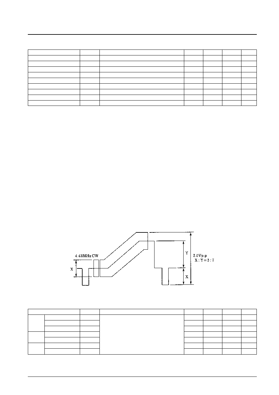
3. Frequency characteristics
For each of the three conditions in Note 2,
V
IN
= 2.0 V
p-p
, V
OUT
(5 MHz)/V
OUT
(100 KHz)
4. Total harmonic distortion (input C = 10 µF)
For each of the three conditions in item 2, measure the total harmonic distortion with V
IN
= 2.0 V
p-p
and f = 1 kHz.
5. Crosstalk
With S6 = 3, measure in the modes for all combinations of S1 to S5 except for the following three conditions: a) S1 = S4 = 1, b) S2 = S5 = 1 and c)
S3 = 1, S4 = S5 = 3.
V
IN
= 2.0 V
p-p
, f = 4.43 MHz, V
OUT
/V
IN
6. Muting circuit crosstalk
With S6 = 1, measure in the modes for all combinations of S1 to S5.
V
IN
= 2.0 V
p-p
, f = 4.43 MHz, V
OUT
/V
IN
7. Output DC offset
Measure the output DC voltage difference between the following modes with S1 = S2 = S3 = 2.
a. S4 = 1, S5 = S6 = 3
b. S5 = 1, S4 = S6 = 3
c. S4 = S5 = S6 = 3
d. S6 = 1, S4 = S5 = 1 or 2
8, 9. Differential gain, differential phase
Switching Characteristics
at Ta = 25∞C, V
CC
= 5 V
No. 4955-2/5
LA7152
Parameter
Symbol
Conditions
min
typ
max
Unit
Current drain
I
CC
*
1
3.0
4.1
5.2
mA
Maximum input level
V
IN
max
*
2
2.0
2.5
Vp-p
Frequency characteristics
Gf
*
3
0
±0.5
dB
Total harmonic distortion
THD
*
4
0.03
0.1
%
Inter-channel crosstalk
CT
C
*
5
≠65
≠60
dB
Muting circuit crosstalk
CT
M
*
6
≠55
≠50
dB
Output DC offset
V
OUT
*
7
5
20
mV
Differential gain
DG
*
8
0.5
1
%
Differential phase
DP
*
9
0.5
1
deg
Parameter
Symbol
Conditions
min
typ
max
Unit
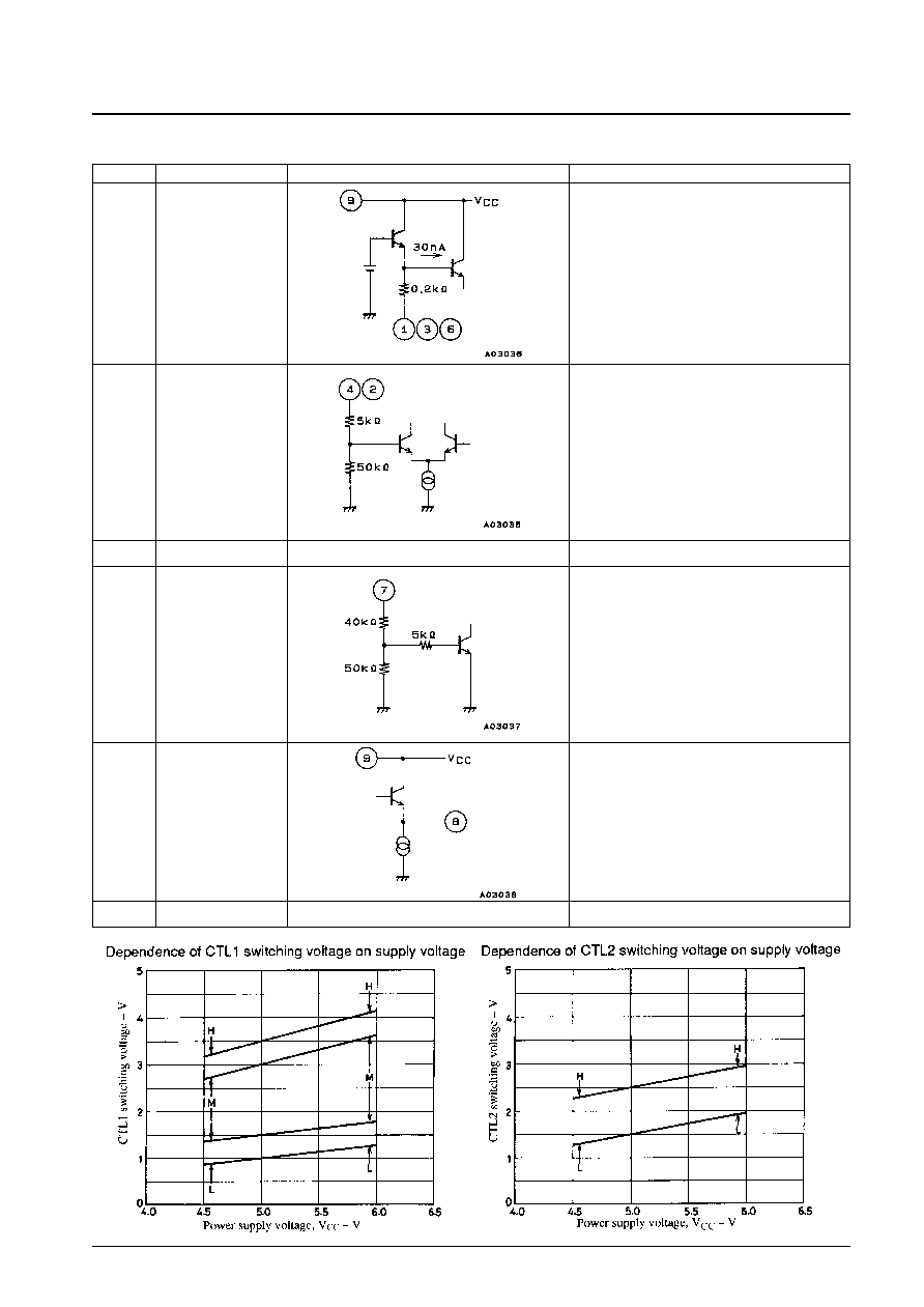
H
V
C1
H
3.5
V
CC
V
CTL1
M
V
C1
M
1.5
3.0
V
L
V
C1
L
In the state with S4 = 2, S5 = 2 and S6 = 2, measure
0
1.0
V
CTL2
H
V
C2
H
the control voltage level when the input signal switches.
2.5
V
CC
V
L
V
C2
L
0
1.5
V
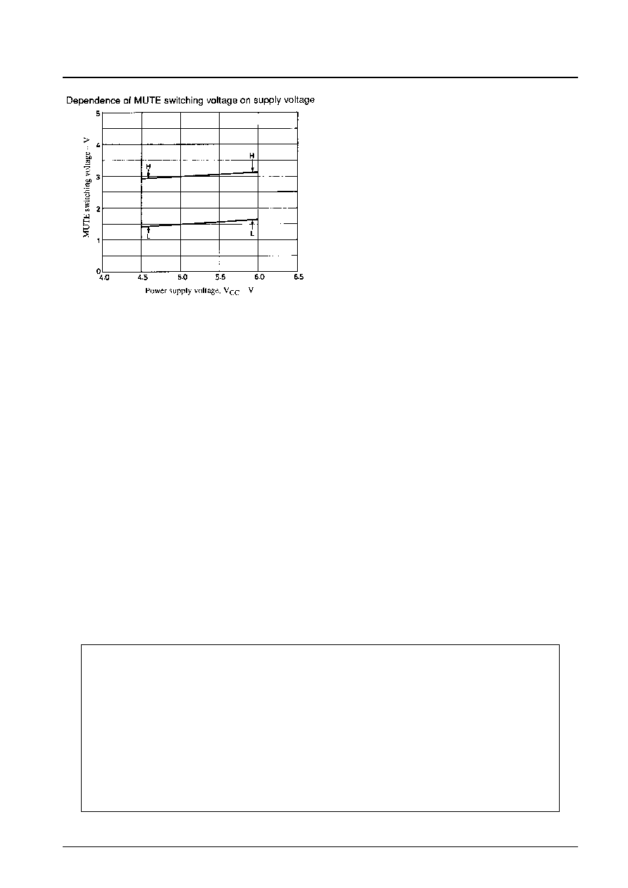
MUTE
H
V
CM
H
3.0
V
CC
V
L
V
CM
L
0
1.5
V
PS No. 4955-5/5
LA7152
This catalog provides information as of December, 1996. Specifications and information herein are subject to
change without notice.
s
No products described or contained herein are intended for use in surgical implants, life-support systems, aerospace
equipment, nuclear power control systems, vehicles, disaster/crime-prevention equipment and the like, the failure of
which may directly or indirectly cause injury, death or property loss.
s
Anyone purchasing any products described or contained herein for an above-mentioned use shall:
Accept full responsibility and indemnify and defend SANYO ELECTRIC CO., LTD., its affiliates, subsidiaries and
distributors and all their officers and employees, jointly and severally, against any and all claims and litigation and all
damages, cost and expenses associated with such use:
Not impose any responsibility for any fault or negligence which may be cited in any such claim or litigation on
SANYO ELECTRIC CO., LTD., its affiliates, subsidiaries and distributors or any of their officers and employees
jointly or severally.
s
Information (including circuit diagrams and circuit parameters) herein is for example only; it is not guaranteed for
volume production. SANYO believes information herein is accurate and reliable, but no guarantees are made or implied
regarding its use or any infringements of intellectual property rights or other rights of third parties.