Overview
The LA7170M is a UHF band RF modulator whose built-
in RF oscillator and mixer make it a single-chip RF
modulator solution. It also supports image positivity
modulation and AM sound modulation for SECAM
systems.
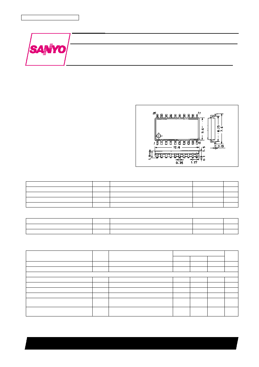
Package Dimensions
unit: mm
3036B-MFP20
Monolithic linear IC
43098HA (OT) No. 5675-1/8
SANYO: MFP20
[LA7170M]
SANYO Electric Co.,Ltd. Semiconductor Bussiness Headquarters
TOKYO OFFICE Tokyo Bldg., 1-10, 1 Chome, Ueno, Taito-ku, TOKYO, 110-8534 JAPAN
RF Modulator for UHF Band (Supports SECAM)
LA7170M
Ordering number : EN5675
Parameter
Symbol
Conditions
Ratings
Unit
Maximum supply voltage
V
CC
max
7
V
Allowable power dissipation
Pd max
Ta
75�C
250
mW
Operating temperature
Topr
�20 to +75
�C
Storage temperature
Tstg
�55 to +150
�C
Specifications
Maximum Ratings
at Ta = 25�C
Parameter
Symbol
Conditions
Ratings
Unit
Recommended operating voltage
V
CC
5.0
V
Operating supply voltage range
V
CC
op
4.5 to 5.5
V
Operating Conditions
at Ta = 25�C
Parameter
Symbol
Conditions
Ratings
Unit
min
typ
max
Current drain 1
I
CC
1
With no input
24
30
36
mA
Regulator voltage
Vreq
With no input
3.7
3.9
4.1
V
[RF Output Level] (S19A: A, S19B: A)
Picture carrier output
P
With no input, with 50
terminator
77
79.5
82
dB�
Sound carrier output ratio
P/S
Ratio of levels at fp and fp+fs
12.5
15
17.5
dB
Sound second harmonic distortion
P/S2
Ratio of levels at fp and fp+2fs
52
62
dB
Sound third harmonic distortion
P/S3
Ratio of levels at fp and fp+3fs
58
68
dB
Chrominance beat
P/CB
Ratio of P above to chrominance beat for
65
75
dB
V
IN
= 0.4 Vp-p with 4.43-MHz sine wave input
Picture harmonic distortion
P/V2
Ratio of P above to level at fp+2 MHz for
50
62
dB
V
IN
= 1 Vp-p with 1-MHz sine wave input
Operating Characteristics
at Ta = 25�C, V
CC
= 5 V, Unless otherwise specified, fp = 591.25 MHz, fs = 5.5 MHz,
S9: ON, S10: B, S19A: B, S19B: B
Continued on next page.
No. 5675-2/8
LA7170M
Continued from preceding page.
Parameter
Symbol
Conditions
Ratings
Unit
min
typ
max
[Picture]
Picture modulation
mp
V
IN
= 1 Vp-p, 100% white
73
80
87
%
Maximum picture modulation
mp max
V
IN
= 1.5 Vp-p, 100% white
88
93
98
%
SYNC compression
(S/V)
V
IN
= 1 Vp-p, 100% white {1�(S/V)(3/7)}
�
100
1.5
5
%
Differential gain
DG
V
IN
: 5-stair step, mp = 80%, at fourth step
2
5
%
Differential phase
DP
V
IN
: 5-stair step, mp = 80%, at fourth step
�6
0
+6
deg
SECAM picture modulation
mp SCM
V
IN
= 1 Vp-p, 100% white S10 : a
88
93
98
%
TSG picture modulation
mp TSG
S9 : off
70
80
90
%
TSG SV ratio
V/S
S9 : off
6.3/3.7
6.8/3.2
7.3/2.7
TSG horizontal period
TS
S9 : off
63.7
64.0
64.3
�s
TSG synchronization pulse width
HS
S9 : off
3.6
4.0
4.4
�s
TSG white signal width
HV
S9 : off
3.6
4.0
4.4
�s
TSG first white rising edge
TV1
S9 : off
22
24
26
�s
TSG second white rising edge
TV2
S9 : off
38
40
42
�s
[Sound]
FM sound modulation
Rank A
73
81
89
%
Rank B
ms FM
81
90
99
%
Rank C
90
100
110
%
Rank D
99
110
121
%
Rank E
109
121
133
%
Interchannel FM sound modulation ratio
ms FM
ms FM ratio with S10: off
0.93
0.98
1.03
FM sound distortion
THD FM
S10: b/off; A
IN
= 1 V
p-p
with 1-kHz sine
0.3
1.0
%
wave input
S10: b/off; V
IN
= 1 Vp-p color bar; A
IN
with
FM sound signal-to-noise ratio
S/NFM
1-kHz sine wave input; ratio of level at A
IN
=
43
55
dB
1 Vp-p to that at A
IN
= 0 Vp-p
Maximum FM modulation
ms max
Maximum modulation possible with S10:
400
%
b/off and sound distortion ratio within 3%
AM sound modulation
ms AM
S10: a; A
IN
= 1 Vp-p with 1-kHz sine wave
43
50
57
%
input
AM sound distortion ratio
THD AM
S10: a; A
IN
= 1 Vp-p with 1-kHz sine wave
0.5
2
%
input
S10: a; V
IN
= 1 Vp-p color bar; A
IN
with 1-kHz
AM sound signal-to-noise ratio
S/N AM
sine wave input; ratio of level at A
IN
= 1 Vp-p
42
47
dB
to that at A
IN
= 0 Vp-p
A
IN
= 1.66 Vp-p with 1-kHz sine wave input;
100% modulation: �50 kHz; S10: b
Note: A
IN
= 1 Vp-p normally produces 60%
modulation.
Note: The AM sound items refer to direct AM detection from the sound carrier (fp + sound intercarrier). This device requires the special care associated with
all high-frequency devices.
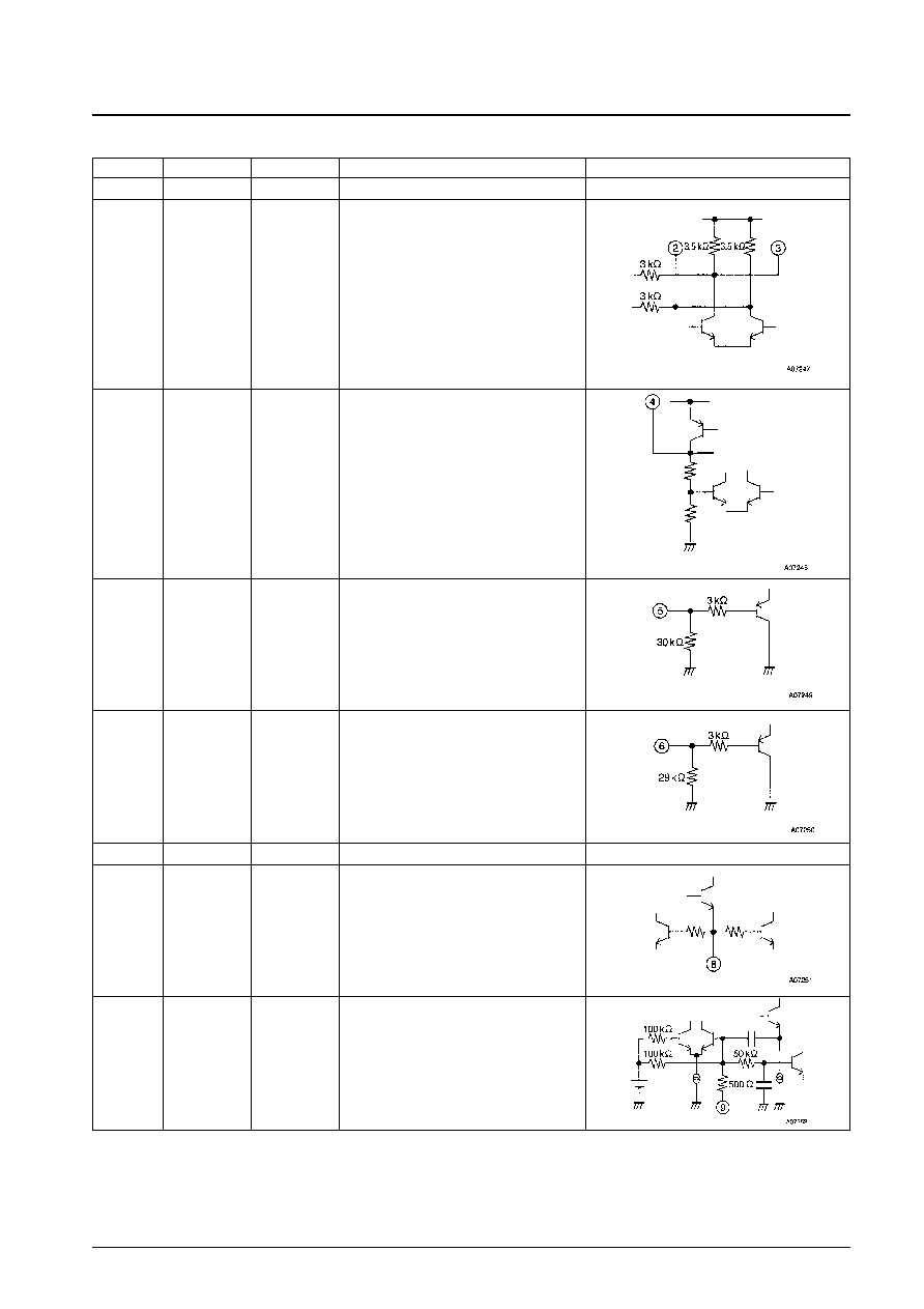
Pin No.
Symbol
Pin Voltage
Pin Description
Equivalent Circuit
5.0
V
CC
for baseband circuits
1
V
CC
1
No. 5675-3/8
LA7170M
Pin Functions
3.9
Connect tank circuits between these pins and the
REG pin.
2
3
TANK1
TANK2
3.9
Regulator output
4
REG
0
FM sound input
5
FM AUDIO IN
0
AM sound input
6
AM AUDIO IN
0
Ground for baseband circuits
7
GND1
3.0
Picture input. Clamp at SYNC tip.
8
VIDEO IN
2.6
(open)
Ground this pin through a 500-kHz oscillator.
Open : TSG ON
GND : TSG OFF
9
RES
Continued on next page.

No. 5675-4/8
LA7170M
Continued from preceding page.
Pin No.
Symbol
Pin Voltage
Pin Description
Equivalent Circuit
2.6
(open)
L (0 to 1.5 V) : PAL-TANK1
M (2.1 to 3.2 V) : PAL-TANK2
H (3.8 to 5.0 V) : SECAM-TANK2
10
FoCTL
2.5
1.8
1.8
2.5
This circuit forms a Colpitts oscillator.
11
12
13
14
OSC-B1
OSC-E1
OSC-E2
OSC-B2
0
Ground for RF oscillator
15
GND2
5.0
V
CC
for RF oscillator
16
V
CC
2
0
V
CC
for RF mixer
17
GND3
1.7
Grounding this pin through a capacitor or resistor
attenuates the sound intercarrier level.
18
P/S
3.0
RF mixer signal output
19
RF OUT
5.0
V
CC
for RF mixer
20
V
CC
3
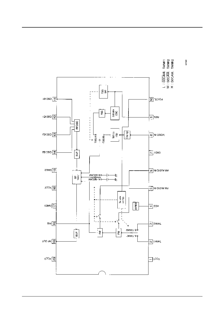
Block Diagram
No. 5675-5/8
LA7170M
No. 5675-6/8
LA7170M
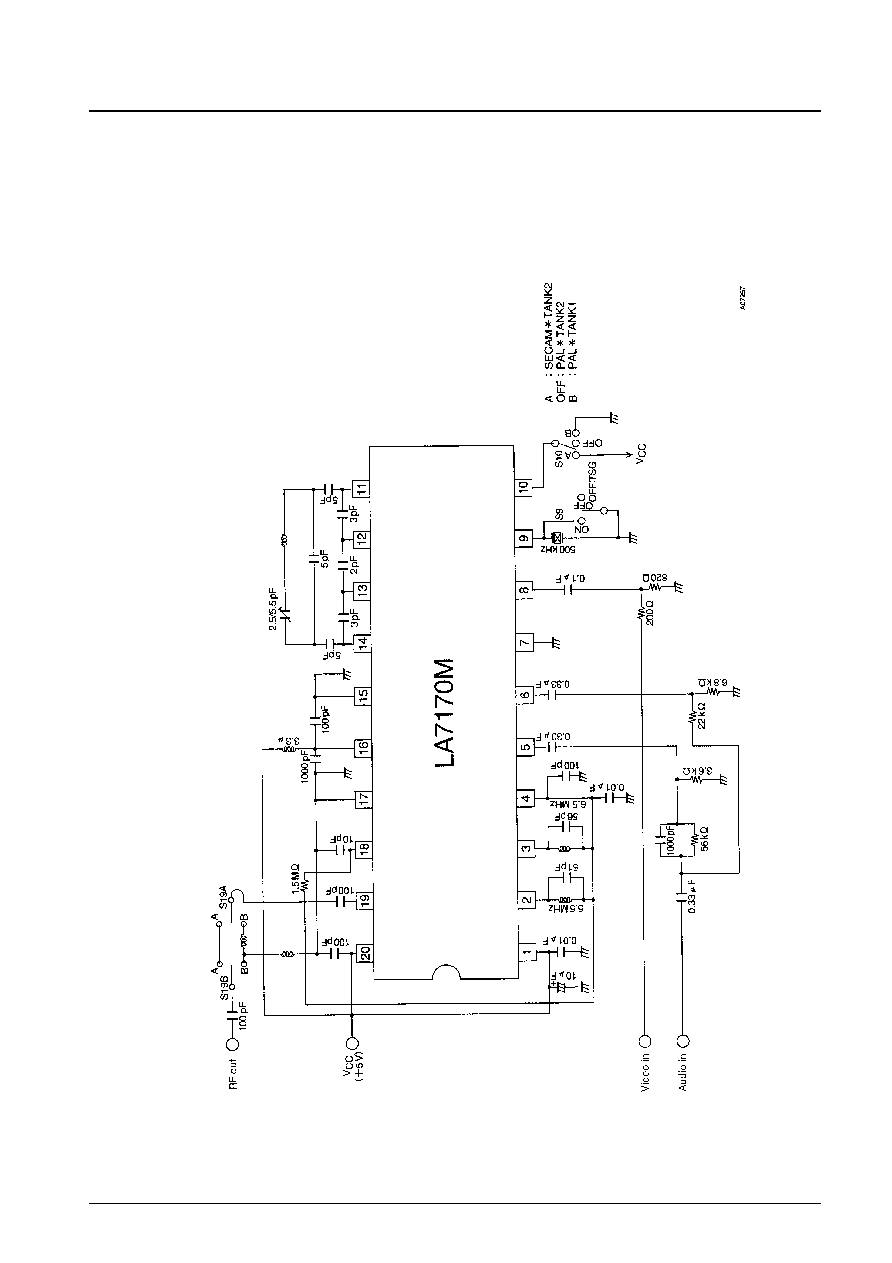
Test Circuit
5.5-MHz coil Sumida Electric SA-1038
6.5-MHz coil Sumida Electric SA-1002
500-kHz resonator Murata CSB500E54
No. 5675-7/8
LA7170M
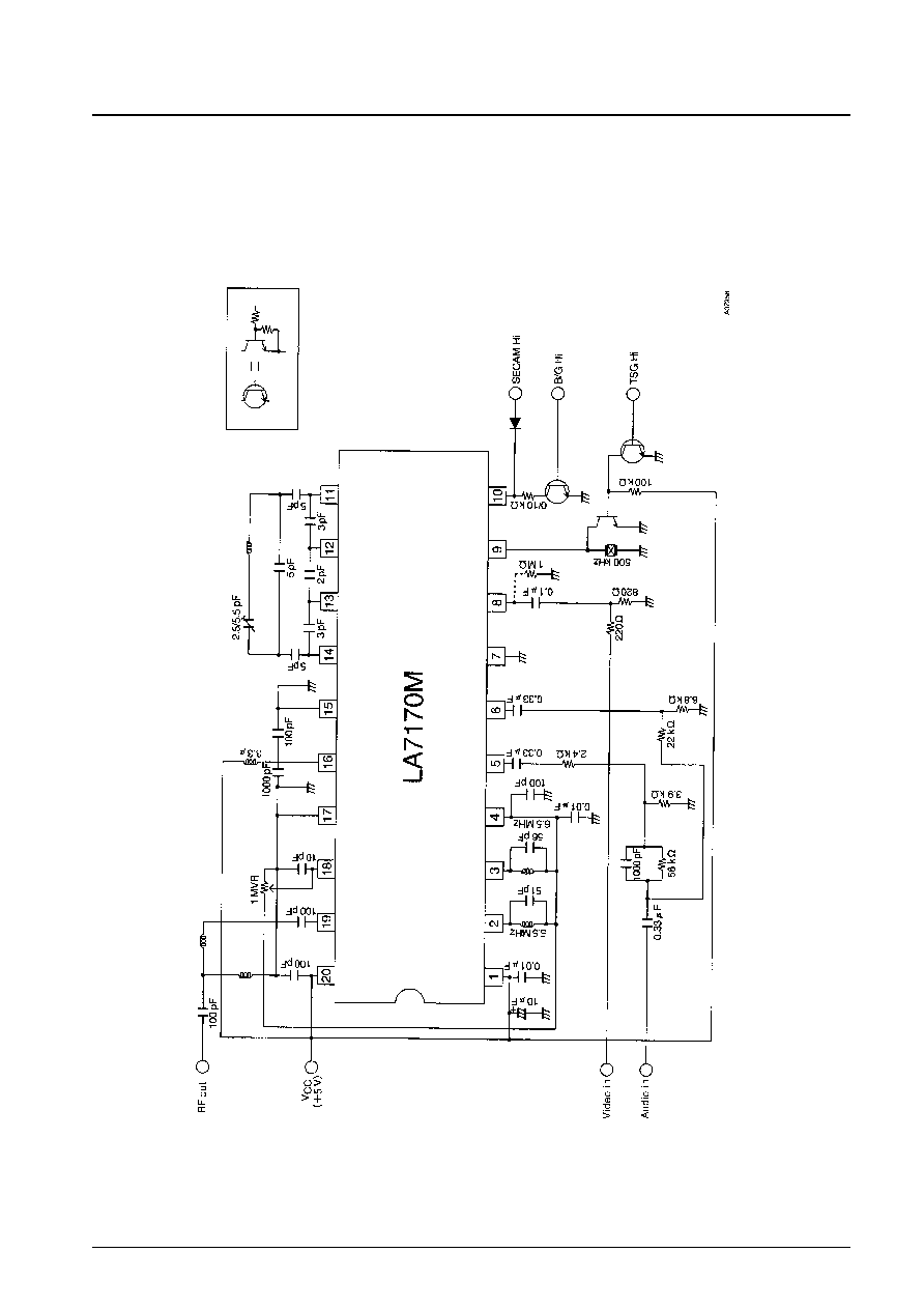
Sample Application Circuit
5.5-MHz coil Sumida Electric SA-1038
6.5-MHz coil Sumida Electric SA-1002
500-kHz resonator Murata CSB500E54

PS No. 5675-8/8
LA7170M
This catalog provides information as of April, 1998. Specifications and information herein are subject to change
without notice.
s
No products described or contained herein are intended for use in surgical implants, life-support systems, aerospace
equipment, nuclear power control systems, vehicles, disaster/crime-prevention equipment and the like, the failure of
which may directly or indirectly cause injury, death or property loss.
s
Anyone purchasing any products described or contained herein for an above-mentioned use shall:
Accept full responsibility and indemnify and defend SANYO ELECTRIC CO., LTD., its affiliates, subsidiaries and
distributors and all their officers and employees, jointly and severally, against any and all claims and litigation and all
damages, cost and expenses associated with such use:
Not impose any responsibility for any fault or negligence which may be cited in any such claim or litigation on
SANYO ELECTRIC CO., LTD., its affiliates, subsidiaries and distributors or any of their officers and employees
jointly or severally.
s
Information (including circuit diagrams and circuit parameters) herein is for example only; it is not guaranteed for
volume production. SANYO believes information herein is accurate and reliable, but no guarantees are made or implied
regarding its use or any infringements of intellectual property rights or other rights of third parties.