53098HA (KT) No.4091-1/7
SANYO Electric Co.,Ltd. Semiconductor Bussiness Headquaters
TOKYO OFFICE Tokyo Bldg., 1-10, 1 Chome, Ueno, Taito-ku, TOKYO, 110-8534 JAPAN
VCR Audio Signal Recording
and Playback Processor
Ordering number:EN4091
LA7285, 7285M
Monolithic Linear IC
r
e
t
e
m
a
r
a
P
l
o
b
m
y
S
s
n
o
i
t
i
d
n
o
C
s
g
n
i
t
a
R
t
i
n
U
e
g
a
t
l
o
v
y
l
p
p
u
s
m
u
m
i
x
a
M
V C
C
x
a
m
4
1
V
e
g
a
t
l
o
v
t
u
p
n
i
1
n
i
P
V N
I 1
C
D
5
6
+
p
-
p
V
t
n
e
r
r
u
c
t
u
p
n
i
1
n
i
P
V N
I 1
5
.
1
�
A
m
n
o
i
t
a
p
i
s
s
i
d
r
e
w
o
p
e
l
b
a
w
o
ll
A
x
a
m
d
P
0
0
4
W
m
e
r
u
t
a
r
e
p
m
e
t
g
n
i
t
a
r
e
p
O
r
p
o
T
5
6
+
o
t
0
1
�
e
r
u
r
t
a
r
e
p
m
e
t
e
g
a
r
o
t
S
g
t
s
T
0
5
1
+
o
t
5
5
�
Ta
65�C
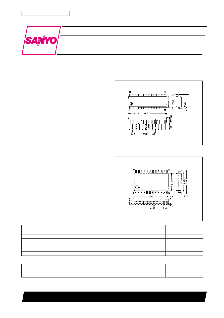
SANYO:DIP24S
Package Dimensions
unit:mm
3067-DIP24S
[LA7285]
Operating Conditions
at Ta=25�C
Overview
The LA7285 and LA7285M include on chip all functions
required for the record and playback of VCR audio
signals. In addition, the inclusion of a switching circuit
for switching between tuner and line input in addition to
the circuits provided by earlier ICs makes the LA7285
truly optimal for audio VCR products.
Funtions
� Equalizer amplifier
� Line amplifier
� Recording/playback switch
� Recording amplifier
� Mute
� SP, LP, EP switch
� Ripple filter
� ALC
� Tape head switch
� Line/tuner input switch
Features
� Built-in input switching circuit (for the line and tuner
inputs).
� Smaller package leaves large space for other
components.
� Equalizer input/output capacitors not required.
� Low gain variation eliminates the need for external
ajustment.
� Supply voltage : 9V and 12V operation.
Specifications
Maximum Ratings
at Ta = 25�C
unit:mm
3112-MFP24S
[LA7285M]
SANYO:MFP24S
r
e
t
e
m
a
r
a
P
l
o
b
m
y
S
s
n
o
i
t
i
d
n
o
C
s
g
n
i
t
a
R
t
i
n
U
e
g
a
t
l
o
v
y
l
p
p
u
s
d
e
d
n
e
m
m
o
c
e
R
V C
C
2
1
V
e
g
n
a
r
e
g
a
t
l
o
v
y
l
p
p
u
s
g
n
i
t
a
r
e
p
O
V C
C
p
o
5
7
.
2
1
o
t
5
.
8
V
�C
�C
LA7285, 7285M
No.4091-2/7
r
e
t
e
m
a
r
a
P
l
o
b
m
y
S
s
n
o
i
t
i
d
n
o
C
s
g
n
i
t
a
R
t
i
n
U
n
i
m
p
y
t
x
a
m
)
E
E
(
n
o
i
t
p
m
u
s
n
o
c
t
n
e
r
r
u
C
I
E
C
C
l
a
n
g
i
s
o
N
5
.
9
0
.
3
1
5
.
6
1
A
m
)
B
P
(
n
o
i
t
p
m
u
s
n
o
c
t
n
e
r
r
u
C
I
P
C
C
l
a
n
g
i
s
o
N
5
.
9
0
.
3
1
5
.
6
1
A
m
)
C
E
R
(
n
o
i
t
p
m
u
s
n
o
c
t
n
e
r
r
u
C
I
R
C
C
l
a
n
g
i
s
o
N
0
.
8
0
.
1
1
0
.
4
1
A
m
]
r
e
i
f
il
p
m
a
r
e
z
il
a
u
q
E
[
n
i
a
g
e
g
a
t
l
o
v
t
i
u
c
r
i
c
-
n
e
p
O
G
V
E
O
VO
V
B
d
7
�
=
0
.
6
6
0
.
1
7
B
d
e
g
a
t
l
o
v
e
s
i
o
n
t
u
p
n
i
t
n
e
l
a
v
i
u
q
E
V
E
I
N
k
2
.
2
=
g
R
r
e
t
li
f
o
i
d
u
A
N
I
D
,
2
.
1
8
.
1
s
m
r
V
�
]
r
e
i
f
il
p
m
a
e
n
i
L
[
)
t
u
p
n
i
B
P
(
n
i
a
g
e
g
a
t
l
o
V
G
V
P
L
VO
V
B
d
7
�
=
0
.
1
2
5
.
1
2
0
.
2
2
B
d
)
t
u
p
n
i
E
N
I
L
,
E
E
(
n
i
a
g
e
g
a
t
l
o
V
G
V
,
E
L
G
V
L
L
VO
V
B
d
7
�
=
0
.
1
2
5
.
1
2
0
.
2
2
B
d
n
o
i
t
r
o
t
s
i
d
c
i
n
o
m
r
a
h
l
a
t
o
T
D
H
T
L
VO
V
B
d
7
�
=
5
0
.
0
3
.
0
%
e
g
a
t
l
o
v
e
s
i
o
n
t
u
p
t
u
O
V
L
O
N
k
2
.
2
=
g
R
r
e
t
li
f
o
i
d
u
A
N
I
D
,
2
7
�
6
6
�
V
B
d
e
g
a
t
l
o
v
t
u
p
t
u
o
m
u
m
i
x
a
M
V
L
M
O
%
1
=
D
H
T
5
.
1
1
.
2
s
m
r
V
n
o
s
i
C
L
A
n
e
h
w
e
g
a
t
l
o
v
t
u
p
t
u
O
V A
O
V N
I
V
B
d
7
2
�
=
0
.
8
�
0
.
7
�
0
.
6
�
V
B
d
t
c
e
f
f
e
C
L
A
C
L
A
V N
I
V
B
d
7
�
o
t
V
B
d
7
2
�
=
0
.
1
0
.
3
B
d
n
o
s
i
C
L
A
n
e
h
w
n
o
i
t
r
o
t
s
i
D
D
H
T
A
V N
I
V
B
d
7
2
�
=
5
0
.
0
6
.
0
%
]
r
e
i
f
il
p
m
a
g
n
i
d
r
o
c
e
R
[
)
n
e
p
o
(
n
i
a
g
e
g
a
t
l
o
V
G
V
R
O
VO
V
B
d
7
�
=
0
.
7
4
0
.
2
5
B
d
)
e
s
l
o
c
(
n
i
a
g
e
g
a
t
l
o
V
G
V
R
O
VO
V
B
d
7
�
=
5
.
2
1
0
.
3
1
5
.
3
1
B
d
n
o
i
t
r
o
t
s
i
d
c
i
n
o
m
r
a
h
l
a
t
o
T
D
H
T
R
VO
V
B
d
7
�
=
1
.
0
3
.
0
%
e
g
a
t
l
o
v
t
u
p
t
u
o
m
u
m
i
x
a
M
V
R
M
O
%
1
=
D
H
T
5
.
1
0
.
2
s
m
r
V
]
t
i
u
c
r
i
c
e
t
u
M
[
e
g
a
t
l
o
v
n
O
V
N
O
M
e
g
a
t
l
o
v
C
D
3
2
n
i
P
5
.
2
0
.
6
V
e
g
a
t
l
o
v
f
f
O
V
F
F
O
M
e
g
a
t
l
o
v
C
D
3
2
n
i
P
0
5
.
1
V
)
E
E
,
B
P
(
n
o
i
t
a
u
n
e
t
t
a
e
t
u
M
MP M
, E
0
8
0
9
B
d
)
C
E
R
(
n
o
i
t
a
u
n
e
t
t
a
e
t
u
M
MR
5
6
5
7
B
d
]
t
i
u
c
r
i
c
h
c
t
i
w
s
P
S
,
P
L
,
P
E
[
e
g
a
t
l
o
v
d
l
o
h
e
d
o
m
P
E
V E
E
e
g
a
t
l
o
v
C
D
1
2
n
i
P
6
.
3
0
.
6
V
e
g
a
t
l
o
v
d
l
o
h
e
d
o
m
P
L
V L
E
e
g
a
t
l
o
v
C
D
1
2
n
i
P
8
.
1
6
.
2
V
e
g
a
t
l
o
v
d
l
o
h
e
d
o
m
P
S
V S
E
e
g
a
t
l
o
v
C
D
1
2
n
i
P
0
0
.
1
V
]
t
i
u
c
r
i
c
h
c
t
i
w
s
B
P
r
e
n
u
T
/
e
n
i
L
[
e
g
a
t
l
o
v
d
l
o
h
e
d
o
m
e
n
i
L
V L
L
e
g
a
t
l
o
v
C
D
2
2
n
i
P
6
.
3
0
.
6
V
e
g
a
t
l
o
v
d
l
o
h
e
d
o
m
r
e
n
u
T
V T
L
e
g
a
t
l
o
v
C
D
2
2
n
i
P
8
.
1
6
.
2
V
e
g
a
t
l
o
v
d
l
o
h
e
d
o
m
B
P
V P
L
e
g
a
t
l
o
v
C
D
2
2
n
i
P
0
0
.
1
V
]
t
i
u
c
r
i
c
h
c
t
i
w
s
E
E
,
C
E
R
[
e
g
a
t
l
o
v
d
l
o
h
e
d
o
m
C
E
R
V R
R
e
g
a
t
l
o
v
C
D
4
2
n
i
P
3
V C
C
V
e
g
a
t
l
o
v
d
l
o
h
e
d
o
m
E
E
V E
R
e
g
a
t
l
o
v
C
D
4
2
n
i
P
0
0
.
1
V
]
h
c
t
i
w
S
t
c
e
l
e
S
d
a
e
H
[
e
c
n
a
t
s
i
s
e
r
n
o
1
n
i
P
R N
O 1
A
m
1
�
=
1
I
0
2
0
3
e
c
n
a
t
s
i
s
e
r
n
o
2
n
i
P
R N
O 2
A
m
1
�
=
2
I
5
0
1
e
g
a
t
l
o
v
t
u
p
n
i
2
n
i
P
V N
I 1
5
4
�
V
Operating Characteristics
at Ta=25�C, VCC=12V, f=1kHz, 0dBV : 1.0 Vrms
Ta=65�C, f=80kHz (sin), ILK=10
�
A
LA7285, 7285M
No.4091-3/7
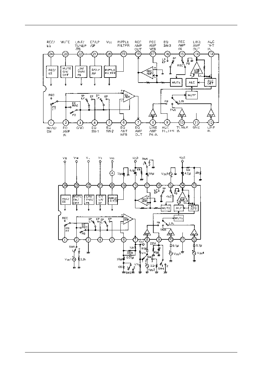
Block Diagram
Test Circuit
Unit (resistance:
, capacitance:F)
LA7285, 7285M
No.4091-4/7
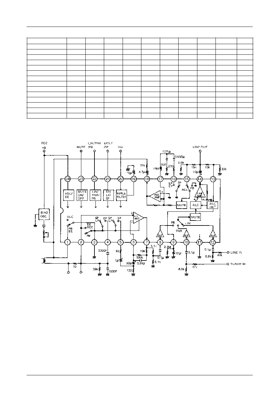
Switch Operation Table
Sample Application Circuit
)
l
o
b
m
y
s
(
m
e
t
i
t
s
e
T
1
W
S
2
W
S
3
W
S
4
W
S
5
W
S
VM
VL
VR
t
u
p
n
I
e
r
u
s
a
e
M
I
E
C
C
2
1
1
2
1
D
N
G
V
5
D
N
G
�
A
I
P
C
C
2
1
1
2
1
D
N
G
D
N
G
D
N
G
�
A
I
R
C
C
2
1
1
2
1
D
N
G
V
5
V
5
�
A
G
V
E
O
1
2
3
2
1
D
N
G
D
N
G
D
N
G
V N
I 1
VO1
V
E
I
N
2
1
3
2
1
D
N
G
D
N
G
D
N
G
�
VO1
G
V
P
L
D
H
T
,
L V
,
L
M
O
2
1
2
2
1
D
N
G
D
N
G
D
N
G
V N
I 2
VO2
G
V
E
L
G
V
,
L
L
2
1
1
2
1
D
N
G
V
5
,
V
5
.
2
D
N
G
V N
I
V
,
3
N
I 4
VO2
V
L
O
N
2
1
3
2
1
D
N
G
V
5
D
N
G
�
VO2
V A
O
D
H
T
,
C
L
A
,
A
2
1
3
1
1
D
N
G
V
5
,
V
5
.
2
D
N
G
V N
I
V
,
3
N
I 4
VO2
G
V
R
O
2
1
3
2
2
D
N
G
V
5
D
N
G
V N
I 5
VO3
O
G
V
R
D
H
T
,
R V
,
R
M
O
2
1
3
2
1
D
N
G
V
5
D
N
G
V N
I 5
VO3
MP
1
1
1
2
1
V
5
D
N
G
D
N
G
V N
I 1
VO2
MR
2
1
1
2
1
V
5
V
5
D
N
G
V N
I 5
VO3
ME
2
1
3
2
1
V
5
V
5
D
N
G
V N
I 2
VO2
Unit (resistance:
, capacitance:F)
LA7285, 7285M
No.4091-5/7
.
o
N
n
i
P
e
m
a
n
n
o
i
t
c
n
u
F
n
i
p
r
o
f
t
i
u
c
r
i
c
l
a
n
r
e
t
n
I
n
o
i
t
c
n
u
f
f
o
n
o
i
t
p
i
r
c
s
e
D
1
1
h
c
t
i
w
s
d
a
e
H
)
e
g
a
t
l
o
v
d
n
a
t
s
h
t
i
w
h
g
i
h
(
B
P
,
E
E
C
E
R
,
f
f
o
f
f
o
e
c
n
a
t
s
i
s
e
r
n
O
0
2
)
p
y
t
(
f
f
o
n
e
h
w
e
g
a
t
l
o
v
d
n
a
t
s
h
t
i
W
V
5
4
�
)
z
H
k
0
8
=
f
(
2
d
n
a
t
u
p
n
i
P
M
A
Q
E
2
h
c
t
i
w
s
d
a
e
H
l
a
n
g
i
s
k
c
a
b
y
a
l
p
r
o
f
e
c
n
a
d
n
e
p
m
i
t
u
p
n
I
d
a
e
h
m
o
r
f
t
u
p
n
i
k
0
8
)
p
y
t
(
C
E
R
,
E
E
n
o
B
P
f
f
o
e
c
n
a
t
s
i
s
e
r
n
O
5
)
p
y
t
(
3
D
N
G
d
n
a
h
c
t
i
w
s
d
a
e
h
1
n
i
p
r
o
f
D
N
G
y
l
n
o
r
e
i
f
il
p
m
A
r
e
z
il
a
u
q
E
4
1
h
c
t
i
w
s
e
d
o
m
P
E
d
n
a
s
d
a
e
h
e
p
a
t
e
g
n
a
h
c
o
t
e
s
U
.
y
c
n
e
u
q
e
r
f
t
n
a
n
o
s
e
r
e
c
n
a
t
s
i
s
e
r
n
O
5
1
)
p
y
t
(
e
c
n
a
d
n
e
p
m
i
t
u
p
n
I
k
0
1
)
p
y
t
(
)
e
d
o
m
P
E
(
5
2
h
c
t
i
w
s
e
d
o
m
P
E
r
e
z
il
a
u
q
E
k
c
a
b
y
a
l
P
e
h
t
s
e
h
c
t
i
w
S
y
c
n
e
u
q
e
r
f
n
o
i
g
e
r
-
h
g
i
h
r
e
i
f
il
p
m
A
.
n
i
a
g
e
g
a
t
l
o
v
e
c
n
a
t
a
t
i
s
e
r
n
O
k
5
1
)
p
y
t
(
e
c
n
a
d
e
p
m
i
t
u
p
n
I
k
0
1
)
p
y
t
(
)
e
d
o
m
P
E
(
6
B
F
N
P
M
A
Q
E
e
v
i
t
a
g
e
n
r
e
i
f
il
p
m
A
r
e
z
il
a
u
q
E
n
i
p
k
c
a
b
d
e
e
f
7
t
u
p
t
u
o
P
M
A
Q
E
8
t
u
p
n
i
B
P
P
M
A
E
N
I
L
e
h
t
m
o
r
f
l
a
n
g
i
s
k
c
a
b
y
a
l
p
e
h
t
s
t
u
p
n
I
e
h
t
e
s
u
a
c
e
B
.
r
e
i
f
il
p
m
A
r
e
z
il
a
u
q
E
K
0
1
1
s
a
h
g
i
h
s
a
s
i
e
c
n
a
d
e
p
m
i
t
u
p
n
i
,
d
e
s
u
e
b
n
a
c
r
o
t
i
c
a
p
a
c
c
i
m
a
r
e
c
F
�
1
.
0
a
.
8
n
i
p
n
o
r
o
t
i
c
a
p
a
c
g
n
il
p
u
o
c
e
h
t
r
o
f
9
R
E
T
L
I
F
C
L
A
n
e
h
w
d
e
m
r
o
f
r
e
p
s
i
n
o
i
t
c
e
t
e
d
e
v
a
W
a
h
g
u
o
r
h
t
D
N
G
o
t
d
e
t
c
e
n
n
o
c
d
n
a
k
c
a
t
t
a
e
h
t
,
n
o
i
t
i
d
d
a
n
I
.
r
o
t
i
c
a
p
a
c
R
d
n
a
C
y
b
t
e
s
s
i
e
m
i
t
y
r
e
v
o
c
e
r
.
s
t
n
a
t
s
n
o
c
e
m
i
t
0
1
t
u
p
n
i
R
E
N
U
T
1
1
D
N
G
e
h
t
t
p
e
c
x
e
s
k
c
o
l
b
t
i
u
c
r
i
c
ll
a
r
o
f
D
N
G
.
r
e
i
f
il
p
m
A
r
e
z
il
a
u
q
E
d
n
a
h
c
t
i
w
s
d
a
e
h
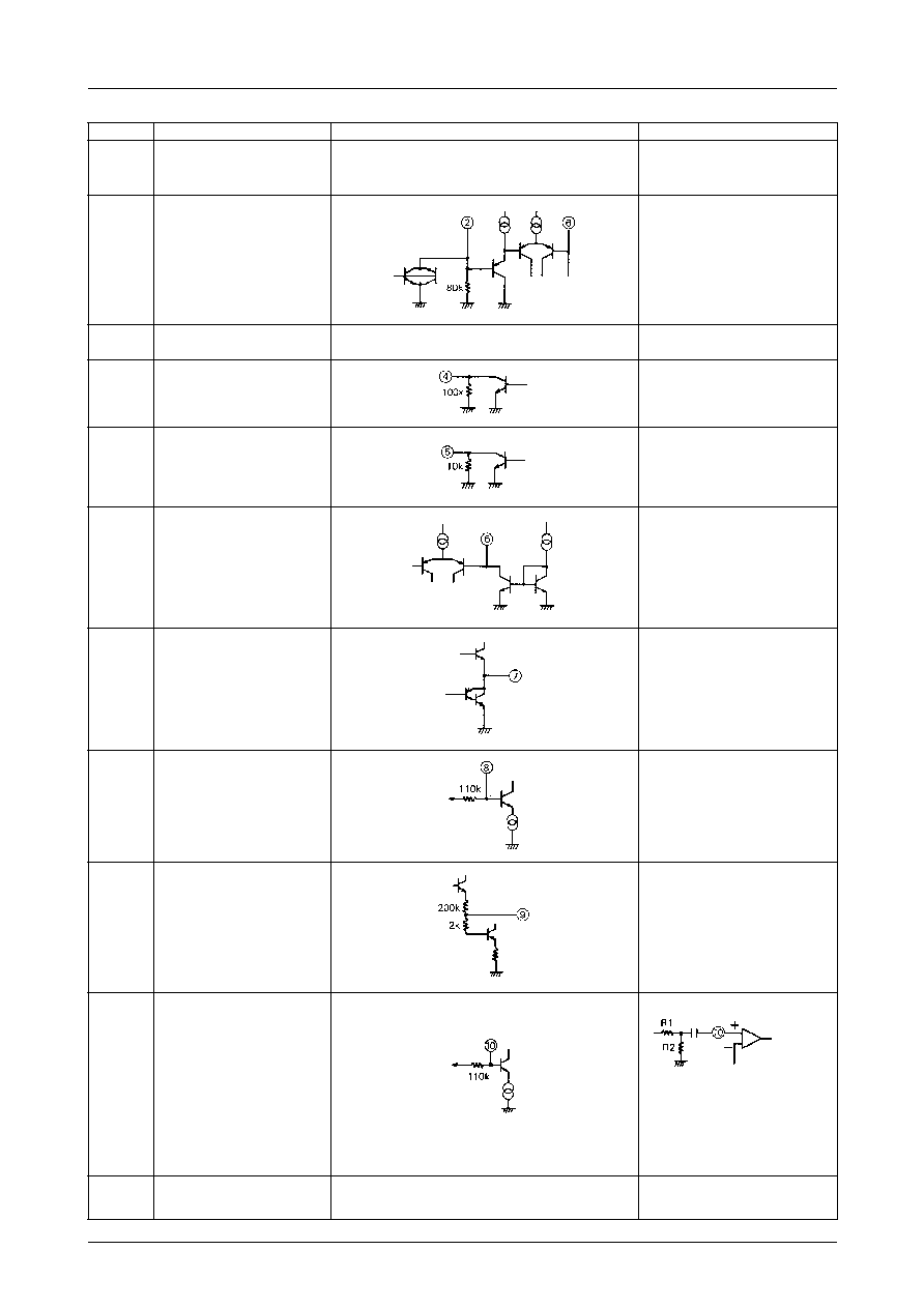
Pin Function
Unit (resistance:
)
Continued to next page.
Inputs EE and REC signals.
The reference input is set by resistors
R1 and R2.
The amplifier gain is fixed at 21.5dB.
In addition, because the input
impedance is as high as 110k
, a 0.1
�
F
ceramic capacitor can be used for the
coupling capacitor on pin 10.
Internal
reference
Internal
reference
LA7285, 7285M
No.4091-6/7
.
o
N
n
i
P
e
m
a
n
n
o
i
t
c
n
u
F
n
i
p
r
o
f
t
i
u
c
r
i
c
l
a
n
r
e
t
n
I
n
o
i
t
c
n
u
f
f
o
n
o
i
t
p
i
r
c
s
e
D
2
1
t
u
p
n
i
E
N
I
L
3
1
n
o
i
t
c
e
t
e
d
e
v
a
w
t
u
p
n
i
C
L
A
4
1
t
u
p
t
u
o
P
M
A
E
N
I
L
5
1
t
u
p
n
i
P
M
A
C
E
R
6
1
h
c
t
i
w
s
e
d
o
m
P
L
7
1
B
F
N
P
M
A
C
E
R
8
1
t
u
p
t
u
o
P
M
A
C
E
R
9
1
r
e
t
li
f
e
l
p
p
i
R
0
2
V
(
e
g
a
t
l
o
v
y
l
p
p
u
S
C
C )
1
2
l
o
r
t
n
o
C
P
S
/
P
L
/
P
E
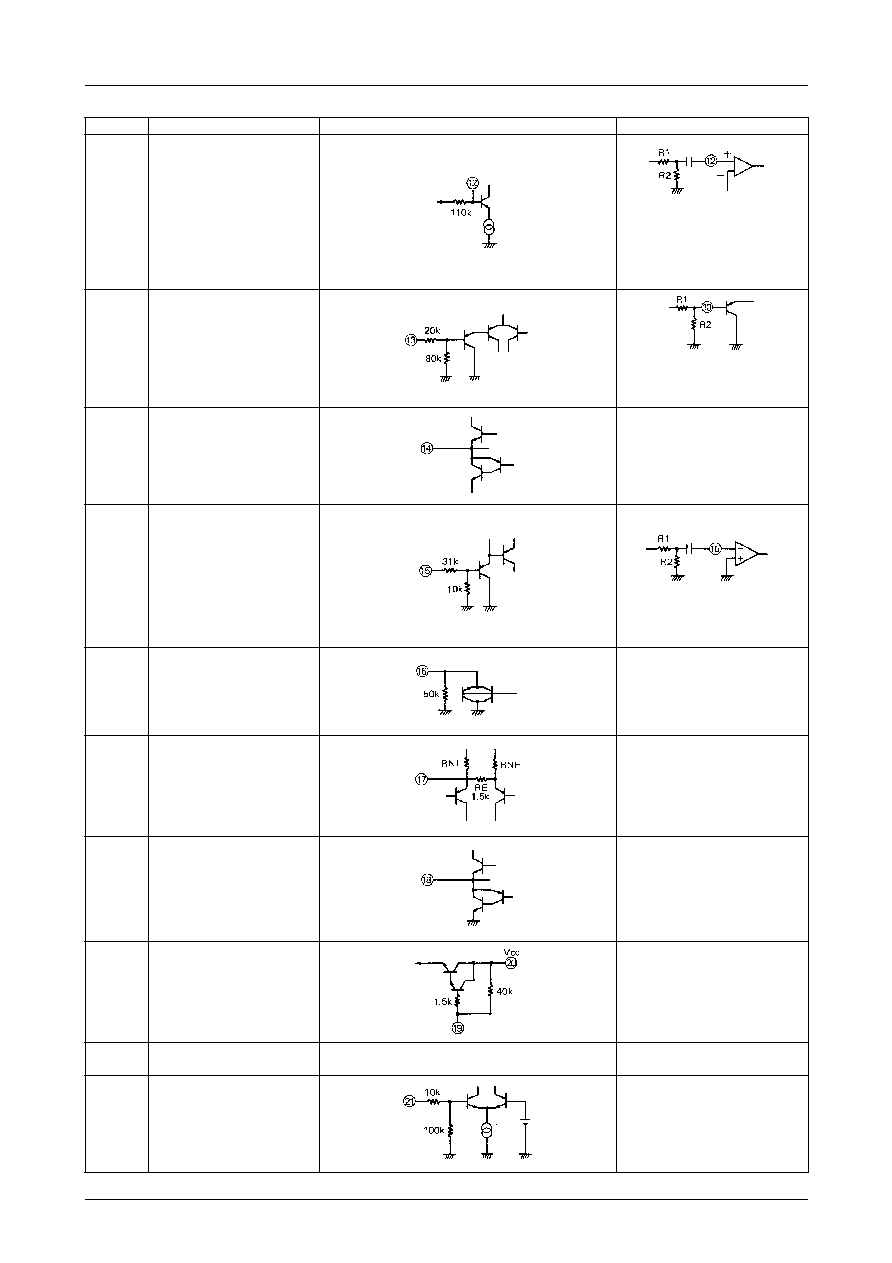
Continued from proceeding page.
Continued to next page.
Unit (resistance:
)
Inputs the Line Amplifier output
signal.
The ALC level is set by the resistors
R1 and R2.
Output inpedance
50
(typ)
Inputs the recording signal from Line
Amplifier.
The recording current is set by the
resistors R1 and R2. A coupling
capacitor is unnecessary as pin 15 is
a zero baias input.
Used to adjust the high-region peaking
frequency during recording amplifier in
LP mode.
On resistance
15
(typ)
Intput inpedance
50
(typ)
Recording amplifier negative-
feedback input. Used to adjust the
high-region peaking frequency of the
recording amplifier with an L, C, R
network connected to ground.
Output inpedance
40
(typ)
Ripple rejection is performed when
connected to GND through an
electrolytic capacitor for the filter.
VCC max=14V
VCC=8.5V to 12.75V
When the voltage on
pin 21 is 3.6V to 6.0V:EP;
when 1.8V to 2.6V:LP;
when 0V to 1.8V:SP
Switch On Pin Number
EP mode:4,5,16
LP mode:16
Inputs EE and RE signals.
The reference input is set by resistors
R1 and R2.The amplifier gain is fixed at
21.5 dB. In addition, because the input
impedance is as high as 110k
, a
0.1
�
F ceramic capacitor can be used
for the coupling capacitor on pin 12.
Internal
reference
Power supply of
each circuit block
LA7285, 7285M
PS No.4091-7/7
No products described or contained herein are intended for use in surgical implants, life-support systems,
aerospace equipment, nuclear power control systems, vehicles, disaster/crime-prevention equipment and
the like, the failure of which may directly or indirectly cause injury, death or property loss.
Anyone purchasing any products described or contained herein for an above-mentioned use shall:
Accept full responsibility and indemnify and defend SANYO ELECTRIC CO., LTD., its affiliates,
subsidiaries and distributors and all their officers and employees, jointly and severally, against any
and all claims and litigation and all damages, cost and expenses associated with such use:
Not impose any responsibilty for any fault or negligence which may be cited in any such claim or
litigation on SANYO ELECTRIC CO., LTD., its affiliates, subsidiaries and distributors or any of
their officers and employees jointly or severally.
Information (including circuit diagrams and circuit parameters) herein is for example only; it is not guarant-
eed for volume production. SANYO believes information herein is accurate and reliable, but no guarantees
are made or implied regarding its use or any infringements of intellectual property rights or other rights of
third parties.
This catalog provides information as of May, 1998. Specifications and information herein are subject to
change without notice.
.
o
N
n
i
P
e
m
a
n
n
o
i
t
c
n
u
F
n
i
p
r
o
f
t
i
u
c
r
i
c
l
a
n
r
e
t
n
I
n
o
i
t
c
n
u
f
f
o
n
o
i
t
p
i
r
c
s
e
D
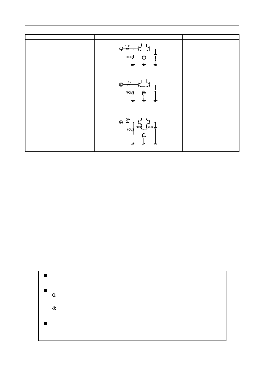
2
2
l
o
r
t
n
o
C
B
P
/
R
E
N
U
T
/
E
N
I
L
n
o
e
g
a
t
l
o
v
e
h
t
n
e
h
W
;
E
N
I
L
:
V
0
.
6
o
t
V
6
.
3
s
i
2
2
n
i
p
R
E
N
U
T
:
V
6
.
2
o
t
V
8
.
1
n
e
h
w
B
P
:
V
0
.
1
o
t
V
0
n
e
h
w
3
2
l
o
r
t
n
o
C
E
T
U
M
n
o
e
g
a
t
l
o
v
e
h
t
n
e
h
W
;
n
o
E
T
U
M
:
V
0
.
6
o
t
V
5
.
2
s
i
3
2
n
i
p
f
f
o
E
T
U
M
:
V
5
.
1
o
t
V
0
n
e
h
w
4
2
l
o
r
t
n
o
C
E
E
/
C
E
R
n
o
e
g
a
t
l
o
v
e
h
t
n
e
h
W
V
o
t
V
5
.
2
s
i
4
2
n
i
p
C
C
;
C
E
R
:
E
E
:
V
0
.
1
o
t
V
0
n
e
h
w
Continued from proceeding page.
Unit (resistance:
)