30706 MS OT B8-7298,B8-5738 No.A0244-1/7
LA73052
Overview
This LA73052 is a 4ch 75
Video Driver IC. The LA73052 is ideal for use the video output driver such as VCR and
DVD-player equipment.
Functions
∑ 6dB AMP+driver (2ch)
∑ 2input-1output SW+6dB AMP+driver (2ch)
Specifications
Maximum Ratings
at Ta = 25
∞C
Parameter Symbol
Conditions
Ratings Unit
Maximum supply voltage
VCC max
±7, +14
V
Allowable power dissipation
Pd max
Ta
80
∞
C
700
mW
Operating temperature
Topr
-20 to +80
∞
C
Storage temperature
Tstg
-55 to +150
∞
C
When mounted on a 114.3
◊
76.1
◊
1.6mm
3
glass epoxy board.
Recommended Operating Conditions
at Ta = 25∞C
Parameter Symbol
Conditions
Ratings Unit
Recommending operation voltage
VCC
±5
+9
V
Operating voltage range
VCC op
±4.0 to ±5.5
V
+8 to +10
Ordering number : ENA0244
Monolithic Linear IC
4ch 75
Video Driver
LA73052
No.A0244-2/7
Electrical Characteristics
at Ta = 25∞C, VCC = ±5V
Ratings
Parameter Symbol
Conditions
min typ max
Unit
Current dissipation
ICC1 No
signal
46.8
55
63.2
mA
Voltage gain
VG
VIN = 1Vp-p, f = 4.43MHz
5.7
6.2
6.7
dB
Frequency
characteristics 1
VF1 VIN = 1Vp-p, f = 100k/5MHz
-1.0
0
1.0
dB
Frequency
characteristics 2
VF2 VIN = 1Vp-p, f = 100k/27MHz
-25
-20
dB
Group delay
GD
f = 100k/4.43MHz
±10
±15
ns
Maximum output level
VO max
f = 1kHz, THD = 1%
3.0
4.0
Vp-p
Control voltage H level
VcntH
Pins 12, 24, 28, 30, 33 input voltage
2.5
VCC
V
Control voltage L level
VcntL
Pins 12, 24, 28, 30, 33 input voltage
0
1.0
V
Design guarantee items
Ratings
Parameter Symbol
Conditions
min typ max
Unit
Video S/N
VG1V
-75 -70
dB
Differential Gain
DG
VIN = 1Vp-p, RAMP signal
1.0
%
Differential Phase
DP
VIN = 1Vp-p, RAMP signal
1.0
deg.
Mute attenuation
VMUTEV
VIN = 1Vp-p, f = 4.43MHz
-60
-55
dB
Cross-talk between
channel
VCTKV
VIN = 1Vp-p, f = 4.43MHz
-60
-55
dB
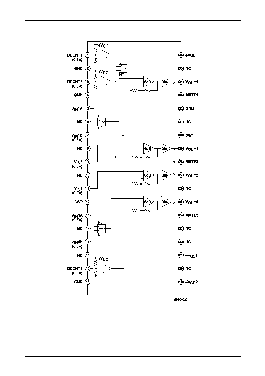
Truth Table
Pin 12
Pin 30
Pins 24, 28, 33
H VIN4A VIN1B THROUTH
L VIN4B VIN1A MUTE
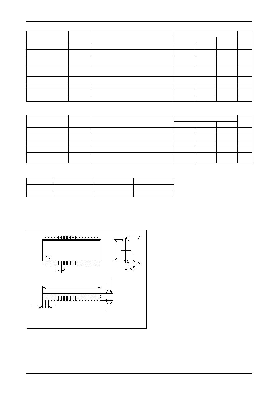
Package Dimensions
unit : mm
3247A
SANYO : SSOP36(275mil)
1
36
18
19
0.8
15.0
0.
5
7.
6
0.2
0.3
(0.7)
5.
6
(1.
5
)
1.
7max
0.
1
LA73052
No.A0244-5/7
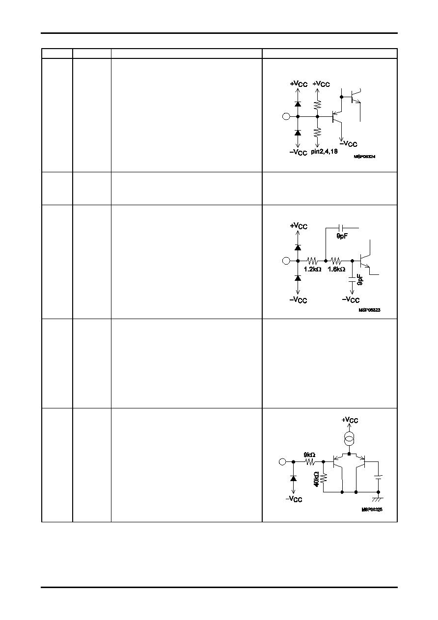
Pin Functions
Pin No.
Pin Name
Terminal Explanation
Equivalent Circuit
1
3
17
DCCNT1
DCCNT2
DCCNT3
DC offset mode charge terminal between input and output.
When a condenser is input at the position between pin 1
(DCCNT1) and GND, the operation of IC becomes the mode
with 0.6V DC offset between input and output of 1ch
(pins 5 and 34).
Similarly when a condenser is input at the position between
pin 3 (DCCNT2) and GND, it becomes the mode with 0.3V DC
offset between input and output of 1, 2, 3ch (pins 7 and 34, pins
9 and 29, pins 11 and 27), and when a condenser is input at the
position between pin 17 (DCCNT3) and GND, it becomes the
mode with 0.3V DC offset between input and output of 4ch
(pins 13 or 15, and pin 31).
And when pins 1, 3, 17 and GND is shorted, it becomes the
mode without DC offset between input and output.
2
4
18
32
GND
Both ±power supply and +power supply are GND.
5
7
9
11
13
15
VIN1A
VIN1B
VIN2
VIN3
VIN4A
VIN4B
Input terminal.
Non-bias. It is possible to use with being directly connected
with DC. When DC coupling, it is necessary to add bias after
the coupling.
6
8
10
14
16
20
22
23
26
31
35
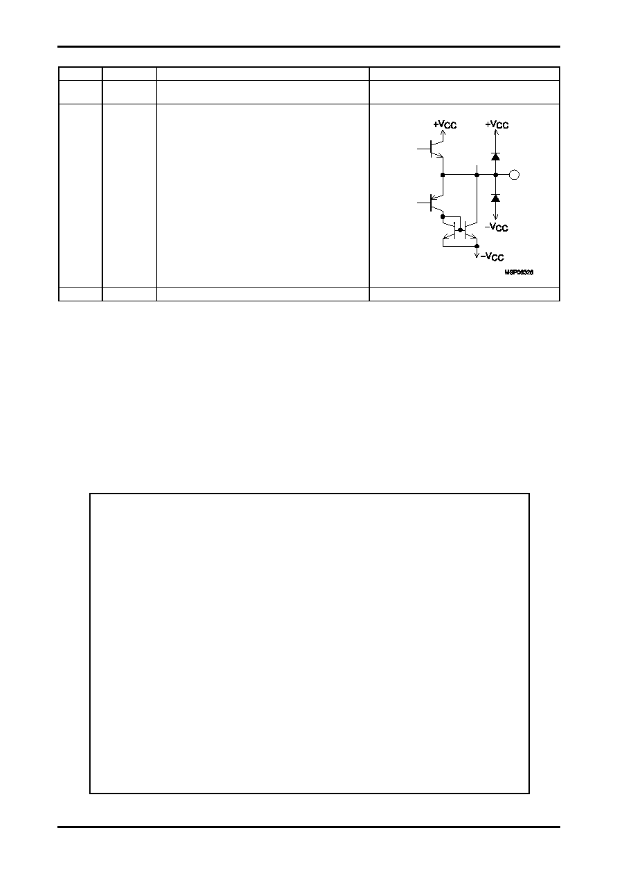
NC
12
24
28
30
33
SW2
MUTE3
MUTE2
SW1
MUTE1
Changeover terminal of Mute or Input Switch
When the Mute terminal is Low, it is Mute.
Changeover of Input Switch is :
SW1 High : VIN1B
Low
:
VIN1A
SW2
High : VIN4A
Low
:
VIN4B
When the terminal is Open, it is Low.
Continued on next page.
LA73052
PS No.A0244-6/7
Continued from preceding page.
Pin No.
Pin Name
Terminal Explanation
Equivalent Circuit
19
21
≠VCC. ≠VCC of using ±power supply. Using +power supply, it is GND.
25
27
29
34
VOUT4
VOUT3
VOUT2
VOUT1
Output terminal
Using ±power supply, in case of the mode with DC offset, it is
possible to use without capacitor of output by setting
pin 5 to 0.6V-bias and by setting pins 7, 9, 11, 13, 15 to
0.3V-bias. And in case of the mode without DC offset, it is
possible to use without capacitor of output by setting each input
to zero-bias. When using +power supply, both of the modes
needs coupling capacitor.
36 +VCC
Both ±power supply and +power supply are +VCC.
This catalog provides information as of March, 2006. Specifications and information herein are subject
to change without notice.
Specifications of any and all SANYO products described or contained herein stipulate the performance,
characteristics, and functions of the described products in the independent state, and are not guarantees of
the performance, characteristics, and functions of the described products as mounted in the customer's
products or equipment. To verify symptoms and states that cannot be evaluated in an independent device,
the customer should always evaluate and test devices mounted in the customer's products or equipment.
SANYO Electric Co., Ltd. strives to supply high-quality high-reliability products. However, any and all
semiconductor products fail with some probability. It is possible that these probabilistic failures could give
rise to accidents or events that could endanger human lives, that could give rise to smoke or fire, or that
could cause damage to other property. When designing equipment, adopt safety measures so that these
kinds of accidents or events cannot occur. Such measures include but are not limited to protective circuits
and error prevention circuits for safe design, redundant design, and structural design.
In the event that any or all SANYO products (including technical data, services) described or contained
herein are controlled under any of applicable local export control laws and regulations, such products must
not be exported without obtaining the export license from the authorities concerned in accordance with the
above law.
No part of this publication may be reproduced or transmitted in any form or by any means, electronic or
mechanical, including photocopying and recording, or any information storage or retrieval system, of
otherwise, without the prior written permission of SANYO Electric Co., Ltd.
Any and all information described or contained herein are subject to change without notice due to
product/technology improvement, etc. When designing equipment, refer to the "Delivery Specification" for
the SANYO product that you intend to use.
Information (including circuit diagrams and circuit parameters) herein is for example only; it is not
guaranteed for volume production. SANYO believes information herein is accurate and reliable, but no
guarantees are made or implied regarding its use or any infringements of intellectual property rights or other
rights of third parties.